Embed Size (px)
Citation preview

NOLTA, IEICE
Paper
Design of load-independent class-Einverter with MOSFET gate-to-drainand drain-to-source parasiticcapacitances
Weisen Luo 1a), Yusuke Ogi 1 , Fumiya Ebihara 1 ,
Xiuqin Wei 1b), and Hiroo Sekiya 2
1 Department of Electrical and Electronic Engineering, Chiba Institute of
Technology, 2–17–1, Tsudanuma, Narashino, Chiba 275–0016, Japan
2 Graduate School of Advanced Integration Science, Chiba University
1–33, Yayoi-cho, Ingae-ku, Chiba 263–8522, Japan
a) [email protected]) [email protected]
Received July 31, 2019; Revised November 18, 2019; Published April 1, 2020
Abstract: This paper presents a numerical design approach of the load-independent class-Einverter with MOSFET gate-to-drain and drain-to-source parasitic capacitances. The designcurves of the load-independent class-E inverter are also given. A design example is shown alongwith its LTspice simulation and laboratory experiment. By applying the proposed designapproach, there are no changes in the output-voltage waveforms and all the switch-voltagewaveforms satisfy the zero-voltage-switching (ZVS) condition even the load-resistance valuevaries from the desired one without applying any tuning processes. Additionally, the resultsobtained from the LTspice simulation and laboratory experiment show quantitative agreementwith the numerical predictions, which shows the effectiveness of the proposed design approachand design curves of the load-independent class-E inverter with MOSFET gate-to-drain anddrain-to-source parasitic capacitances given in this paper.
Key Words: load-independent, class-E inverter, zero-voltage-switching condition, MOSFETdrain-to-source parasitic capacitance, MOSFET gate-to-drain parasitic capacitance
1. IntroductionThe class-E inverter is one of switching-mode inverters and it adapts single-end circuit topology [1–32]. The advantage of the single-ended circuit topology is that it requires only one switch, which isconducive to the realization of the driving circuits, especially at high frequencies. Additionally, sinceits switch voltage satisfies the ZVS condition, a high power-conversion efficiency can be obtained athigh frequencies. Therefore, it has been widely concerned by academics and industrialists.
267
Nonlinear Theory and Its Applications, IEICE, vol. 11, no. 2, pp. 267–277 c©IEICE 2020 DOI: 10.1587/nolta.11.267

Fig. 1. Load-independent class-E inverter. (a) Circuit topology. (b) Equiv-alent circuit.
The class-E inverter, however, imposes restrictions on practical applications due to its sensitivecharacteristic to the load variation. In general, the loads are dynamic in the practical applications. Inthe class-E inverter, once the load varies from the desired value, the output-voltage waveform changesand the ZVS loses, which result in a degradation of the performance and efficiency. To solve the issue,a new design conception was shown in [29, 30]. The circuit topologies of the class-E inverter with thenew design conception introduced in [29] and [30] and the typical class-E inverter are identical. Theinput inductor based on the load-independent design conception, however, works as a finite inductorinstead of a RF bulk choke, which has the input current changed to provide a required amplitude andphase shift that the output-voltage waveform and the ZVS operation can be kept even the load varies.Meanwhile, it is possible to obtain a faster transient performance and smaller circuit scale because ofthe adoption of the finite input inductor in the load-independent class-E inverter compared with thetypical class-E inverter.
[29, 30], however, did not consider the effects of the MOSFET parasitic capacitances. The shuntcapacitance, which is connected between the drain and the source of the MOSFET in parallel, isan important element of the class-E inverter to satisfy the ZVS condition. In general, the shuntcapacitance is composed of both the external capacitance and the MOSFET drain-to-source parasiticcapacitance. At low frequencies, the MOSFET drain-to-source parasitic capacitance can be neglectedbecause the external capacitance is dominant in the shunt capacitance. The value of the total shuntcapacitance, however, decreases as the operating frequency increases. In other words, the ratio ofthe MOSFET drain-to-source parasitic capacitance to the total shunt capacitance increases as theoperating frequency increases [8–17]. On the other hand, the gate-to-drain parasitic capacitance isconnected in series to the driving signal source, which are connected between the MOSFET drainport and source one. Therefore, the gate-to-drain parasitic capacitance can be regarded to possessthe same function as one of the shunt capacitance and it’s necessary to consider its effect. In otherwords, it is important to consider the effects of both the MOSFET gate-to-drain and drain-to-sourceparasitic capacitances at high-frequency operations [8–12]. There are, however, no research worksto consider the effects of the MOSFET gate-to-drain parasitic capacitance and the drain-to-sourceparasitic capacitance of the load-independent class-E inverter for achieving the class-E ZVS conditionand constant output ac voltage.
This paper presents a numerical design approach of the load-independent class-E inverter withMOSFET gate-to-drain and drain-to-source parasitic capacitances. And its design curves are given.A design example is also shown along with its LTspice simulation and laboratory experiment. Thereare no changes in the output-voltage waveforms and all the switch-voltage waveforms satisfy theZVS condition even the load-resistance value varies from the desired one. Additionally, the resultsobtained from the LTspice simulation and laboratory experiment show quantitative agreement withthe numerical predictions, which has shown the effectiveness of the design approach and design curvesof the load-independent class-E inverter with MOSFET gate-to-drain and drain-to-source parasiticcapacitances.
2. Load-independent class-E inverter
Figure 1(a) shows the circuit topology of the load-independent class-E inverter. The load-independentclass-E inverter has a simple circuit topology just like the typical class-E inverter and is composedof a dc-supply voltage source VI , an input inductor Li, MOSFET as a switching device S, a shunt
268

Fig. 2. Example waveforms of the load-independent class-E inverter for D =0.5.
capacitor CS , a series resonant filter L − C, and load resistor R.Figure 2 shows the example waveforms of the load-independent class-E inverter for the switch-on
duty ratio D = 0.5. In this figure, θ = ωt = 2πf represents the angular time and f is the operatingfrequency. For the load-independent class-E inverter, the switch S is driven by the input voltageDr as shown in Fig. 2 and turns on and off alternately. When the switch S turns off, the sum ofthe currents through the input inductor and the output series resonant filter flows through the shuntcapacitance CS and produces the switch voltage vS . And when the switch is at the turns-on instant,the switch voltage vS satisfies the ZVS condition,
vS(π) = 0. (1)
Because of the ZVS condition, the switching power losses are minimized. Therefore, the load-independent class-E inverter can achieve a high efficiency at high frequencies.
3. Design procedureIn this section, we consider the effects of the MOSFET gate-to-drain and drain-to-source parasiticcapacitances and give the design procedure for the load-independent class-E inverter. The designapproach is based on the design procedure in [31]. By applying this numerical design procedure, it ispossible to obtain the accurate design values easily for achieving multiple design restrictions.
3.1 AssumptionsIn this paper, the load-independent class-E inverter is designed with the following assumptions:
1) The shunt capacitance is composed of the external capacitance Cext and the MOSFET drain-to-source parasitic capacitance Cds. Additionally, the MOSFET drain-to-source parasitic ca-pacitance has nonlinear characteristic and is expressed as [11–17]
Cds =Cj0(
1 +vS
Vbi
)m , (2)
where Vbi is the built-in potential, which typically ranges from 0.5 to 0.9 V, Cj0 is the capacitanceat vS = 0, and m is the grading coefficient of the diode junction.
2) The MOSFET gate-to-drain parasitic capacitance Cgd is regarded as a linear one [8–12]. Theassumptions 1) and 2) follow PSpice MOSFET models, which have a nonlinear drain-to-sourceparasitic capacitance and a linear gate-to-drain parasitic capacitance.
3) The equivalent series resistances (ESRs) of all the inductors are considered. The ESRs of allthe capacitors, however, are ignored because they are much smaller than ESRs of the inductors.
4) All the passive elements except the MOSFET drain-to-source parasitic capacitance work aslinear elements.
269

Table I. Switching pattern of the load-independent class-E inverter withMOSFET gate-to-drain and drain-to-source parasitic capacitances.
0 < θ ≤ π π < θ ≤ 2π
Dr OFF ON
5) The switch S has zero switching time, infinite off resistance, and on resistance ron.
6) The switch S turns off at θ = 0 and the switch-on duty ratio D = 0.5. Therefore, its switchingpatterns are given as Table I.
7) The driving signal source is an ideal voltage source as shown in Fig. 1(a).
Using the above assumptions, the equivalent circuit of the load-independent class-E inverter withthe MOSFET gate-to-drain and drain-to-source can be obtained as shown in Fig. 1(b).
3.2 ParametersIn this paper, following parameters are defined for the inverter designs.
a) A = fo/f = 1/(2πf√
LC): The ratio of the resonant frequency to the operating frequency.
b) B = C/(Cgd+Cext): The ratio of the resonant capacitance to the sum of the MOSFET gate-to-drain capacitance and external capacitance.
c) H = L/Li: The ratio of the resonant inductance to the input inductance.
d) Q = ωL/R: The loaded quality factor in the series resonant filter.
e) Bnon = Cj0/(Cgd+Cext): The ratio of the MOSFET drain-to-source capacitance at vS = 0 tothe sum of the MOSFET gate-to-drain capacitance and external capacitance.
3.3 Circuit equationsThe operations in the range of 0 < θ ≤ 2π are considered for the design of the load-independent class-E inverter with MOSFET gate-to-drain and drain-to-source parasitic capacitances and its circuitequations are given as follows,⎧⎪⎪⎪⎪⎪⎪⎪⎪⎪⎪⎪⎪⎪⎪⎨
⎪⎪⎪⎪⎪⎪⎪⎪⎪⎪⎪⎪⎪⎪⎩
dii
dθ=
H
QR(VI − vS − rLiii)
dio
dθ=
1QR
[vS − vC − (R + rL)io]
dvS
dθ=
A2BQR
1 +Bnon
(1 + vS/Vbi)m
(ii −
vS
rS− io
)
dvC
dθ= A2QRio
(3)
where rLi and rL are the ESRs of the input inductor Li and resonant inductor L, respectively. AndrS is the equivalent resistance of the switch S. In this paper, rS is expressed as
rS =
{ron rS is in the on − state,∞ rS is in the off − state.
(4)
Additionally, when we define x(θ) = [x1, x2, x3, x4]T = [ii, io, vS , vC ]T ∈ R4. (3) can be rewritten as
dx
dθ= f(θ, x,λ) (5)
where λ = [A,B,H,Q,Bnon, rS , R, Vbi,m]T ∈ R9.
270

Table II. The parameters of MOSFETs.
ron Cj0 Cgd Vbi m
IRF510 0.54 Ω 367 pF 40.1 pF 0.8 V 0.5IRF520 0.27 Ω 622 pF 137 pF 0.8 V 0.5IRF530 0.16 Ω 1151 pF 178 pF 0.8 V 0.5
3.4 Design conditionsThe load-independent class-E inverter with MOSFET gate-to-drain and drain-to-source parasitic ca-pacitances should operate in the steady state, achieving the switching condition. The steady-stateconditions of the driver are
x(2π) − x(0) = 0 ∈ R4 (6)
which are the boundary conditions at θ = 0 and θ = 2π. The ZVS condition shown in (1) is mandatoryto achieve. Additionally, the phase shift of the output current is zero. This is also one of the restrictconditions, which guarantees a constant output voltage even the load changes [29, 30].
ϕ = 0, (7)
where ϕ is the initial phase shift of the output current.From the above, it can be seen that the design of the load-independent class-E inverter with
MOSFET gate-to-drain and drain-to-source parasitic capacitances is regarded to solve the algebraicequations shown in (1), (6), and (7). In these equations, there are 6 algebraic equations and 4 unknownparameters. Therefore, 2 parameters can be set as the design parameters from λ9. In this paper,we selected the parameters A and B as the unknown parameters and gave the other parameters asdesign specifications. In order to obtain the values of the unknown parameters, the Newton’s methodis applied to solve the algebraic equations. It is possible to derive the algebraic-equation solutionsnumerically. The algorithm of the Newton’s method was presented in [31] in detail. Additionally, forobtaining the initial values of the currents and voltages of the circuit equations in (3), the Runge-Kuttamethod is used.
4. Design curvesIn this section, design curves of the load-independent class-E inverter with the MOSFET gate-to-drain and drain-to-source parasitic capacitances are shown by using the design procedure presentedin the previous section. Firstly, the design specifications of the load-independent class-E inverter withMOSFET gate-to-drain and drain-to-source parasitic capacitances were given as follows: D = 0.5,f = 4 MHz, R = 20.0 Ω, and Q = 10.0. Additionally, IRF510, IRF520, and IRF530 MOSFETs byInternational Rectifier were selected as examples for considering the effects of their parasitic capac-itances. And from the PSpice model of IRF510, IRF520, and IRF530 MOSFETs, their parameterswere obtained as shown in Table II. IRF510, IRF520, and IRF530 MOSFETs’ PSpice models aregiven in the Appendix, respectively. The parameters Vbi, m, and Cj0 are identical to Pb, Mj , and Cbd
in the MOSFET model, respectively. In addition, the MOSFET gate-to-drain parasitic capacitanceis obtained as Cgd = W × Cgdo [12]. Note that all the ESRs of the inductors are zero for calculatingthe design curves.
Figure 3 shows the design parameters as functions of H for fixed values of VI/Vbi and three types ofMOSFETs, respectively. It is seen from Fig. 3(a) that A increases as H increases and A increasinglyapproaches to 1 with the increase of H. Namely, the resonant frequency of the series resonant filterL−C is closer to the operating frequency with the increase of H. Additionally, A increases as VI/Vbi
increases. It is seen from Figs. 3(b) and (c) that B and Bnon increase with H decreases regardless ofVI/Vbi and MOSFET type. In particular, the larger Cj0 and Cgd are, namely, the larger the MOSFETparasitic capacitances are, the more significantly B and Bnon vary for small H. It can be also seenfrom Figs. 3(b) and (c) that the smaller VI/Vbi is, the larger B and Bnon are for the same MOSFETwhen H is small.
271

Fig. 3. Design parameters as functions H for fixed values of VI/Vbi in theload-independent class-E inverter. (a) Design curves of A. (b) Design curvesof B. (c) Design curves of Bnon.
5. Output power and power output capabilityFigure 4 shows the normalized peak values of both the switch voltages and the switch currents, outputpowers, and power output capabilities. VSM and ISM are the peak values of the voltages and currentsat the MOSFETs, which can be expressed as
VSM = max {vS} and ISM = max {iS} . (8)
The normalized output powers can be obtained as
PoR
V 2I
=(
Vo
VI
)2
, (9)
where Vo/VI is a root-mean-square value of the normalized output voltage vo/VI and can be given by
Vo
VI=
√12π
∫ 2π
0
[vo(θ)VI
]2dθ. (10)
And cp is the power output capability and can be expressed as
cp =Po
VSMISM. (11)
It is seen from Figs. 4(a) and (b) that the peak values of the switch voltages decrease as H increases,on the contrary, the peak values of the switch currents increase as H increases regardless of VI/Vbi
and MOSFET type. It is also seen from Fig. 4(c) that the normalized output powers decrease as H
increases regardless of VI/Vbi and MOSFET type. Additionally, the larger the MOSFET parasiticcapacitances are, the larger the normalized output powers are. Figure 4(d) shows the power outputcapabilities as functions of H for fixed VI/Vbi and three types of MOSFETs. It can be seen from
272
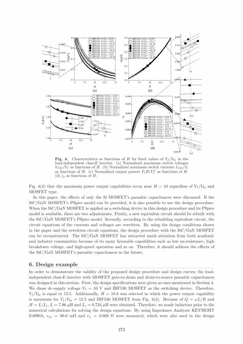
Fig. 4. Characteristics as functions of H for fixed values of VI/Vbi in theload-independent class-E inverter. (a) Normalized maximum switch voltagesVSM/VI as functions of H. (b) Normalized maximum switch currents ISM/II
as functions of H. (c) Normalized output powers PoR/V 2I as functions of H.
(d) cp as functions of H.
Fig. 4(d) that the maximum power output capabilities occur near H = 10 regardless of VI/Vbi andMOSFET type.
In this paper, the effects of only the Si MOSFET’s parasitic capacitances were discussed. If theSiC/GaN MOSFET’s PSpice model can be provided, it is also possible to use the design procedure.When the SiC/GaN MOSFET is applied as a switching device in this design procedure and its PSpicemodel is available, there are two adjustments. Firstly, a new equivalent circuit should be rebuilt withthe SiC/GaN MOSFET’s PSpice model. Secondly, according to the rebuilding equivalent circuit, thecircuit equations of the currents and voltages are rewritten. By using the design conditions shownin the paper and the rewritten circuit equations, the design procedure with the SiC/GaN MOSFETcan be reconstructed. The SiC/GaN MOSFET has attracted much attention from both academicand industry communities because of its many favorable capabilities such as low on-resistance, highbreakdown voltage, and high-speed operation and so on. Therefore, it should address the effects ofthe SiC/GaN MOSFET’s parasitic capacitances in the future.
6. Design example
In order to demonstrate the validity of the proposed design procedure and design curves, the load-independent class-E inverter with MOSFET gate-to-drain and drain-to-source parasitic capacitanceswas designed in this section. First, the design specifications were given as ones mentioned in Section 4.We chose dc-supply voltage VI = 10 V and IRF530 MOSFET as the switching device. Therefore,VI/Vbi is equal to 12.5. Additionally, H = 10.8 was selected in which the power output capabilityis maximum for VI/Vbi = 12.5 and IRF530 MOSFET from Fig. 4(d). Because of Q = ωL/R andH = L/Li, L = 7.96 μH and Li = 0.734 μH were obtained. Therefore, we made inductors prior to thenumerical calculations for solving the design equations. By using Impedance Analyzer KEYSIGHTE4990A, rLi = 90.6 mΩ and rL = 0.608 Ω were measured, which were also used in the design
273
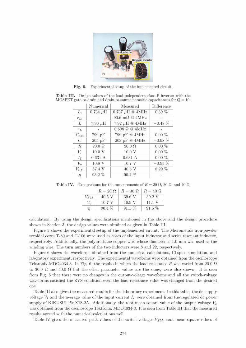
Fig. 5. Experimental setup of the implemented circuit.
Table III. Design values of the load-independent class-E inverter with theMOSFET gate-to-drain and drain-to-source parasitic capacitances for Q = 10.
Numerical Measured DifferenceLi 0.734 μH 0.737 μH @ 4MHz 0.39 %rLi - 90.6 mΩ @ 4MHz -L 7.96 μH 7.92 μH @ 4MHz −0.48 %rL - 0.608 Ω @ 4MHz -
Cext 799 pF 799 pF @ 4MHz 0.00 %C 205 pF 203 pF @ 4MHz −0.98 %R 20.0 Ω 20.0 Ω 0.00 %VI 10.0 V 10.0 V 0.00 %II 0.631 A 0.631 A 0.00 %Vo 10.8 V 10.7 V −0.93 %
VSM 37.4 V 40.5 V 8.29 %η 93.2 % 90.4 % -
Table IV. Comparisons for the measurements of R = 20 Ω, 30 Ω, and 40 Ω.
R = 20 Ω R = 30 Ω R = 40 ΩVSM 40.5 V 39.6 V 39.2 VVo 10.7 V 10.9 V 11.1 Vη 90.4 % 91.1 % 91.5 %
calculation. By using the design specifications mentioned in the above and the design procedureshown in Section 3, the design values were obtained as given in Table III.
Figure 5 shows the experimental setup of the implemented circuit. The Micrometals iron-powdertoroidal cores T-80 and T-106 were used as cores of the input inductor and series resonant inductor,respectively. Additionally, the polyurethane copper wire whose diameter is 1.0 mm was used as thewinding wire. The turn numbers of the two inductors were 8 and 22, respectively.
Figure 6 shows the waveforms obtained from the numerical calculations, LTspice simulation, andlaboratory experiment, respectively. The experimental waveforms were obtained from the oscilloscopeTektronix MDO4034-3. In Fig. 6, the results in which the load resistance R was varied from 20.0 Ωto 30.0 Ω and 40.0 Ω but the other parameter values are the same, were also shown. It is seenfrom Fig. 6 that there were no changes in the output-voltage waveforms and all the switch-voltagewaveforms satisfied the ZVS condition even the load-resistance value was changed from the desiredone.
Table III also gives the measured results for the laboratory experiment. In this table, the dc-supplyvoltage VI and the average value of the input current II were obtained from the regulated dc powersupply of KIKUSUI PMX18-2A. Additionally, the root mean square value of the output voltage Vo
was obtained from the oscilloscope Tektronix MDO4034-3. It is seen from Table III that the measuredresults agreed with the numerical calculations well.
Table IV gives the measured peak values of the switch voltages VSM , root mean square values of
274

Fig. 6. Waveforms of the load-independent class-E inverter with theMOSFET gate-to-drain and drain-to-source parasitic capacitances. (a)For numerical calculation. (b) For LTspice simulation. (c) For laboratoryexperiment.
the output voltages Vo, and power-conversion efficiencies η of R = 20 Ω, 30 Ω, and 40 Ω. It canseen from Table IV that there are no significant changes in the peak values of the switch voltages,root mean square values of the output voltages, and power-conversion efficiencies for the effects ofvariations in the load resistance. The measured power-conversion efficiency increased a little with theload resistance increased. This is because the ESRs of the inductors are intrinsic values and theireffects weaken with the load resistance increase, though the ESRs of the inductors are one of losssources. It can be stated from these results that the design approach and design curves of the load-independent class-E inverter considering the effects of the MOSFET gate-to-drain and drain-to-sourceparasitic capacitances presented in this paper are effective.
In fact, there is an allowable variation range of the load resistance. According to [32], if theloaded quality factor Q is high enough (Q ≥ 2.5), the shape of the waveform of the load currentis approximately sinusoidal. According to the definition of Q = ωL/R, the maximum variable loadresistance Rmax occurs at Q = 2.5 due to the fixed L and ω. Therefore, Rmax = 80 Ω can beobtained from the design values given in the paper. On the other hand, when the load resistancebecomes smaller than the desired one, the MOSFET switch duty ratio would change and the switchcurrent become negative. When the switch current is negative, the antiparallel diode will be ON, andZVS condition is still achieved [32]. The antiparallel diode, however, causes power loss because of itsforward voltage drop, which leads to a reduction in efficiency. Therefore, the desired load resistancecan be regarded as the minimum variable one Rmin. Namely, Rmin = R = 20 Ω in this paper.
7. ConclusionThis paper has presented a numerical design approach of the load-independent class-E inverter withMOSFET gate-to-drain and drain-to-source parasitic capacitances. The design curves were derived.A design example was also shown along with its LTspice simulation and laboratory experiment. Therewere no changes in the output-voltage waveforms and all the switch-voltage waveforms satisfied theZVS condition even the load-resistance value was changed from the desired one. Additionally, theresults obtained from the LTspice simulation and laboratory experiment show quantitative agreementwith the numerical predictions, which showed the accuracy of the proposed design approach and designcurves given in this paper and demonstrated the importance of considering the load-independent class-E inverter with MOSFET gate-to-drain and drain-to-source parasitic capacitances.
AcknowledgmentsThe IRF510, IRF520, and IRF530 MOSFET models used in this paper is obtained from the defaultpackage of PSpice, which are licensed by Cadence. The IRF510, IRF520, and IRF530 MOSFETparameters are shown as follows,.model IRF510 NMOS(Level=3 Gamma=0 Delta=0 Eta=0 Theta=0 Kappa=0.2 Vmax=0 Xj=0
275

Tox=100n Uo=600 Phi=.6 Rs=.4508 Kp=20.68u W=.64 L=2u Vto=3.697 Rd=21.08m Rds=444.4KCbd=366.5p Pb=.8 Mj=.5 Fc=.5 Cgso=600.5p Cgdo=62.71p Rg=2.977 Is=202.9f N=1 Tt=135n)Int’l Rectifier pid=IRFC110 case=TO22088-08-25 bam creation.model IRF520 NMOS(Level=3 Gamma=0 Delta=0 Eta=0 Theta=0 Kappa=0.2 Vmax=0 Xj=0Tox=100n Uo=600 Phi=.6 Rs=.1459 Kp=20.79u W=.73 L=2u Vto=3.59 Rd=80.23m Rds=444.4KCbd=622.1p Pb=.8 Mj=.5 Fc=.5 Cgso=517.9p Cgdo=137.3p Rg=6.675 Is=2.438p N=1 Tt=137n)Int’l Rectifier pid=IRFC120 case=TO22088-08-25 bam creation.model IRF530 NMOS(Level=3 Gamma=0 Delta=0 Eta=0 Theta=0 Kappa=0.2 Vmax=0 Xj=0Tox=100n Uo=600 Phi=.6 Rs=58.53m Kp=20.73u W=.68 L=2u Vto=3.191 Rd=38.69m Rds=444.4KCbd=1.151n Pb=.8 Mj=.5 Fc=.5 Cgso=876.7p Cgdo=261.4p Rg=4.63 Is=1.861p N=1 Tt=125n)Int’l Rectifier pid=IRFC130 case=TO22088-08-25 bam creation
References[1] N.O. Sokal and A.D. Sokal, “Class E—A new class of high efficiency tuned single-ended switching
power amplifier,” IEEE J. Solid-State Circuits, vol. SC-10, no. 3, pp. 168–176, June 1975.[2] F.H. Raab, “Effects of circuit variations on the class-E tuned power amplifier,” IEEE J. Solid-
State Circuits, vol. SC-13, no. 2, pp. 239–247, April 1978.[3] M.K. Kazimierczuk, “Class E tuned power amplifier with shunt inductor,” IEEE J. Solid-State
Circuits, vol. SC-16, no. 1, pp. 2–7, February 1981.[4] M.K. Kazimierczuk, “Effects of the collector current fall time on the class E tuned power
amplifier,” IEEE J. Solid-State Circuits, vol. SC-18, no. 2, pp. 181–193, April 1983.[5] M.K. Kazimierczuk, “Collector amplitude modulation of the class E tuned power amplifier,”
IEEE Trans. Circuits Syst., vol. CAS-31, no. 6, pp. 543–549, June 1984.[6] M.K. Kazimierczuk and K. Puczko, “Exact analysis of class E tuned power amplifier at any Q
and switch duty cycle,” IEEE Trans. Circuits Syst., vol. CAS-34, no. 2, pp. 149–159, February1987.
[7] M.K. Kazimierczuk and K. Puczko, “Class E tuned power amplifier with antiparallel diode orseries diode at switch, with any loaded Q and switch duty cycle,” IEEE Trans. Circuits Syst.,vol. 36, no. 9, pp. 1201–1209, September 1989.
[8] D.K. Choi and S.I. Long, “The effect of transistor feedback capacitance in class-E power am-plifiers,” IEEE Trans. Circuits Syst. I, vol. 50, no. 12, pp. 1556–1559, December 2003.
[9] Z. Liao and X. Zhu, “Analysis and simulation of feedback capacitance effect in class-E poweramplifiers,” in Proc. IEEE ICMMT, Nanjing, China, pp. 1495–1498, April 2008.
[10] D.K. Choi and S.I. Long, “A physically based analytic model of FET class E power amplifiers-designing for maximum PAE,” IEEE Trans. Microw. Theory Tech., vol. 47, no. 9, pp. 1712–1720,September 1999.
[11] X. Wei, H. Sekiya, S. Kuroiwa, T. Suetsugu, and M.K. Kazimierczuk, “Effect of MOSFETgate-to-drain parasitic capacitance on class-E power amplifier,” in Proc. IEEE ISCAS, Paris,France, pp. 3200–3203, June 2010.
[12] X. Wei, H. Sekiya, S. Kuroiwa, T. Suetsugu, and M.K. Kazimierczuk, “Design of class-E am-plifier with MOSFET linear gate-to-drain and nonlinear drain-to-source capacitances,” IEEETrans. Circuits Syst. I, vol. 58, no. 10, pp. 2556–2565, October 2011.
[13] M.J. Chudobiak, “The use of parasitic nonlinear capacitors in class-E amplifiers,” IEEE Trans.Circuits Syst. I, vol. 41, no. 12, pp. 941–944, December 1994.
[14] T. Suetsugu and M.K. Kazimierczuk, “Comparison of class E amplifier with nonlinear and linearshunt capacitance,” IEEE Trans. Circuits Syst. I, vol. 50, no. 8, pp. 1089–1097, August 2003.
[15] T. Suetsugu and M.K. Kazimierczuk, “Analysis and design of class E amplifier with shuntcapacitance composed of nonlinear and linear shunt capacitances,” IEEE Trans. Circuits Syst.I, vol. 51, no. 7, pp. 1261–1268, July 2004.
276

[16] H. Sekiya, Y. Arifuku, H. Hase, J.M. Lu, and T. Yahagi, “Investigation of class-E amplifier withnonlinear capacitance for any output Q and finite DC-feed inductance,” IEICE Trans. Fundam.,vol. E89-A, no. 4, pp. 873–881, April 2006.
[17] A. Mediano, P.M. Gaudo, and C.K. Bernal, “Design of class E amplifier with nonlinear andlinear shunt capacitances for any duty cycle,” IEEE Trans. Microw. Theory Tech., vol. 55,no. 3, pp. 484–492, March 2007.
[18] C. Yoo and Q. Huang, “A common-gate switched 0.9-W class-E power amplifier with 41% PAEin 0.25-μm CMOS,” IEEE J. Solid-State Circuits, vol. 36, no. 5, pp. 823–830, May 2001.
[19] J. Ramos, K. Francken, G.G.E. Gielen, and M.S.J. Steyaert, “An efficient, fully parasitic-awarepower amplifier design optimization tool,” IEEE Trans. Circuits Syst., vol. 52, no. 8, pp. 1526–1534, August 2005.
[20] N.O. Sokal, “Class E RF power amplifiers,” QEX, no. 204, pp. 9–20, January/February 2001.[21] F. del Aguila, P. Pala, J. Bonet, and R. Giralt, “A technique for maximum efficiency class-E
amplifier design,” in Proc. ECCTD’03, Cracow, Poland, pp. 281–284, September 2003.[22] H. Sekiya and M.K. Kazimierczuk, “Design of RF-choke inductors using core geometry coeffi-
cient,” in Proc. EMCW2009, Nashville, USA, September 2009.[23] N. Sagawa, H. Sekiya, and M.K. Kazimierczuk, “Computer-aided design for class-E switching
circuits taking into account optimized inductor design,” in Proc. IEEE APEC, California, USA,pp. 2212–2219, February 2010.
[24] K. Shinoda, T. Suetsugu, M. Matsuo, and S. Mori, “Analysis of phase-controlled resonant DC-AC inverters with class E amplifier and frequency multipliers,” IEEE Trans. Ind. Eletron.,vol. 45, no. 3, pp. 412–420, June 1998.
[25] D. Kessler and M.K. Kazimierczuk, “Power losses and efficiency of Class-E power amplifier atany duty ratio,” IEEE Trans. Circuits Syst. I, vol. 51, no. 9, pp. 1675–1689, September 2004.
[26] T. Suetsugu and M.K. Kazimierczuk, “Maximum operating frequency of class-E amplifier atany duty ratio,” IEEE Trans. Circuits Syst. II, vol. 55, no. 8, pp. 768–770, August 2008.
[27] M.K. Kazimierczuk, “Exact analysis of class E tuned power amplifier with only one inductorand one capacitor in load network,” IEEE J. Solid-State Circuits, vol. SC-18, no. 2, pp. 214–221,April 1983.
[28] M.K. Kazimierczuk, RF Power Amplifiers. New York, NY: John Wiley & Sons, 2008.[29] R.E. Zulinski and K.J. Grady, “Load-independent class E power inverter. I. Theoretical de-
velopment,” IEEE Trans. Circuits Syst. I, Reg. Papers, vol. 37, no. 8, pp. 1010–1018, August1990.
[30] S. Aldhaher, D.C. Yates, and P.D. Mitcheson, “Load-independent class E/EF inverters and rec-tifiers for MHz-switching applications,” IEEE Trans. Power Electron., vol. 33, no. 10, pp. 8270–8287, October 2018.
[31] H. Sekiya, T. Ezawa, and Y. Tanji, “Design procedure for class-E switching circuits allowingimplicit circuit equations,” IEEE Trans. Circuits Syst. I Reg. Papers, vol. 55, no. 11, pp. 3688–3696, November 2008.
[32] M.K. Kazimierczuk and D. Czarkowski, Resonant Power Converters. New York, NY: JohnWiley & Sons, 2011.
277