Embed Size (px)
DESCRIPTION
econfigurable_Antenna
Citation preview

IEEE TRANSACTIONS ON ANTENNAS AND PROPAGATION, VOL. 62, NO. 12, DECEMBER 2014 6049
Miniaturized Reconfigurable Multiband Antenna ForMultiradio Wireless Communication
Mojtaba Fallahpour, Member, IEEE, Mohammad Tayeb Ghasr, Senior Member, IEEE, and R. Zoughi, Fellow, IEEE
Abstract—This paper introduces a general methodical approachfor designing frequency reconfigurable antennas. This method wassuccessfully used to design a novel coplanar waveguide (CPW)-fedslot frequency reconfigurable antenna capable of operating atfour preselected frequency bands distributed over a wide fre-quency range from 59.5 MHz to 1000 MHz (i.e., 4 octavesof bandwidth) while keeping its overall size as small as possible.To add reconfigurablility to the antenna, optimally-designed andelectronically-controllable PIN diode-loaded slots were used tostrategically manipulate the flow of current path and consequentlychange the characteristics of the antenna. Designing for the lowestoperating frequency (59.5 MHz), capacitor-loaded meandered slotlines and reconfigurable matching network were implemented tokeep the size of the antenna as small as possible. The resultingoverall size of the antenna is only where iscalculated at 59.5 MHz. The measurement results verified that theantenna successfully operates at 59.25–59.75 MHz, 314–398 MHz,430–496 MHz, and 792–950 MHz, all with an almost omnidirec-tional pattern and an acceptable gain.
Index Terms—Miniaturization, multiradio wireless communica-tion, reconfigurable antennas, small antennas, software defined an-tennas, ultra-wideband antennas.
I. INTRODUCTION
T HERE is a growing interest in wireless communicationmarket toward integrating more and more radios into a
single chip (or single wireless platform) [1]. These multiradioplatforms (e.g., laptop computer) require compact antennas op-erating over a wide range of frequencies, or antennas that can betuned at those desired frequencies [1]. Relative form-factor (i.e.,overall dimensions and bulkiness) prevents the use of many in-dividual antennas to address this problem. Wideband or ultra-wideband (UWB) antennas may be considered as a solution.
Manuscript received March 10, 2014; revised August 24, 2014; accepted Oc-tober 17, 2014. Date of publication October 22, 2014; date of current versionNovember 25, 2014. Research was sponsored by the Army Research Laboratoryand was accomplished under Cooperative Agreement Number W911NF-10-2-0077. The views and conclusions contained in this document are those of theauthors and should not be interpreted as representing the official policies, eitherexpressed or implied, of the Army Research Laboratory or the U.S. Govern-ment. The U.S. Government is authorized to reproduce and distribute reprintsfor Government purposes not withstanding any copyright notation herein.M. Fallahpour is with the Electrical and Computer Engineering Department,
University of Illinois at Urbana-Champaign, Champaign, IL 61801, USA(e-mail: [email protected]).M. T. Ghasr and R. Zoughi are with the Applied Microwave Nondestruc-
tive Testing Laboratory, Electrical and Computer Engineering Department, Mis-souri University of Science and Technology, Rolla, MO 65409, USA (e-mail:[email protected]; [email protected]).Color versions of one or more of the figures in this paper are available online
at http://ieeexplore.ieee.org.Digital Object Identifier 10.1109/TAP.2014.2364293
In the past several decades, much work has been done to de-velop wideband and UWB antennas for applications such as:high-resolution microwave imaging, short-range wireless com-munication systems, wireless body area network (WBAN), andelectromagnetic compatibility measurements [2]–[5]. However,noise and interference issues along with large relative form-factor, limit the utility of wideband/UWB antennas for the mul-tiradio communication purposes [1]. As another potential solu-tion, multiband antennas, which can simultaneously cover somepreselected and distinct bands [6]–[8], also suffer from noiseand interference issues [1]. Additionally, when a desired op-erating frequency is relatively low [e.g., in the ultra-high-fre-quency (UHF) or very-high-frequency (VHF) regions], keepingthe form-factor small becomes a challenge. In contrast, recon-figurable antennas are capable of addressing many of these lim-itations [1], [9]–[17]. A reconfigurable antenna can electron-ically or mechanically switch among different configurationsto provide for a set of desired characteristics (e.g., matchingover a range of frequency, pattern, and polarization). In com-parison with wideband antennas, reconfigurable antennas offeradvantages such as: compact size, similar gain and radiation pat-tern for the preselected desired frequency bands, efficient use ofelectromagnetic spectrum, frequency selectivity useful for noiseand interference reduction and polarization diversity [1], [14].Despite these advantages, the topic of reconfigurable antennasis relatively new, and there is not a general, robust and method-ical design procedure for such antennas [15]. Moreover, to ourknowledge, there are not many compact planar reconfigurableantennas which can cover preselected frequency bands in a rel-atively wide bandwidth.To this end, here we introduce a methodical approach for
designing a reconfigurable antenna operating at several prese-lected frequency bands. Then, based on this design approach,the implementation of a novel coplanar waveguide (CPW)-fedreconfigurable antenna is given. The designed antenna coversfour distinct preselected bands in the VHF/UHF regions. To addreconfigurablility to the antenna, optimally designed slots whichare loaded with electronically controllable PIN diodes are used.Moreover, to extend the frequency of operation to below 100MHz while keeping the form-factor of the antenna as small aspossible, capacitor-loaded meandered slot lines and a reconfig-urable matching network are used. The overall size of the an-tenna is where is corresponding wave-length to the lowest operating frequency by the antenna (i.e.,
equivalent to ). Consequently,this design offers a significant improvement in comparison withother works (e.g., reported work in [18]) for miniaturization pur-poses in VHF band. Moreover, the covered distinct bands are
0018-926X © 2014 IEEE. Personal use is permitted, but republication/redistribution requires IEEE permission.See http://www.ieee.org/publications_standards/publications/rights/index.html for more information.

6050 IEEE TRANSACTIONS ON ANTENNAS AND PROPAGATION, VOL. 62, NO. 12, DECEMBER 2014
distributed in a frequency range from 59.5 MHz to 1000MHz which translates into about four octaves of bandwidth.
II. DESIGN APPROACH
In general, defining goals, requirements, and constraints areconsidered as the first critical steps in antenna design and imple-mentation. These may include desired antenna characteristics,physical sizes, mechanical and manufacturing constraints, etc.Then, an initial appropriate antenna type should be selected[19]. For regular static (i.e., nonreconfigurable) antennas withfixed electrical and geometrical characteristics, the designprocedure is usually straightforward, and the antenna typemay be selected based on the requirements. For instance, fora narrowband, compact antenna that must conform to a planarstructure microstrip antennas are good candidates. However,by changing one of the requirements (e.g., bandwidth), themicrostrip structure may no longer be the optimum choice.After selecting the antenna type, analytical or numerical designequations from literature (e.g., [19]), or full-wave numericalelectromagnetic solvers such as CST Microwave Studio orHFSS [20], [21] may be used to simulate the characteristics ofthe antenna. Then, this is followed by constructing the antennaand comparing its measured critical characteristics with thoseobtained by the simulations and ultimately with the designrequirements.Designing a reconfigurable antenna with dynamically
changing characteristics, is not as straightforward as designinga regular static antenna. To address this issue, a design method-ology for frequency reconfigurable antennas is proposed here.Similar to the static antenna design, one must have a cleardefinition of design objectives, requirements, and constraintsfor reconfigurable antenna design. Subsequent to sorting thedesired frequency bands in an ascending order, it is then con-venient to designate the bands from 1 to where the bandwith the lowest center frequency is designated to as Band 1and the band with the highest center frequency is designatedas Band . Subsequently, the procedure continues in Step 1by designing an antenna which covers the highest band (Band) having the shortest wavelength. The static antenna design
procedure can be invoked to perform this design. Meanwhile,the antenna type should be selected in a way to provide suf-ficient flexibility for the additional required reconfigurablilitymodifications (as will be seen). This is a critical issue for thereconfigurable antenna design, making it distinguishable fromthe static antenna design. Unlike wire antennas (i.e., dipole),antennas designed based on microstrip and CPW structuresprovide the designer with good flexibility for manipulating theground plane or the signal or current density path in order tochange its characteristics. For future references, the designedantenna covering Band is called Antenna . Step 2involves manipulating Antenna to achieve Antennacovering the next lower Band . For a CPW-basedantenna, this can be achieved by incorporating slots into theground plane, causing the current flow path to change andsubsequently the desired characteristics of the antenna. Byoptimizing the location and dimension of such slots, the an-tenna may cover Band . Then, the same procedure isused to design Antenna to cover Band
, respectively.
Fig. 1. Flow-chart for designing frequency reconfigurable antennas.
It should be possible to switch between characteristics of An-tenna 1 and characteristics of any other interim antenna suchas Antenna by a few short or open circuits. Theseshorts and opens can be electronically/mechanically realized onAntenna 1 using switches. After adding actual switches to An-tenna 1 (i.e., Step ), the antenna is called “reconfig-urable antenna” because one single antenna provides dif-ferent “configurations” and at each of these configurations itmimics the characteristics of corresponding antenna (e.g., Con-figuration mimics Antenna ). Also, it is important todesign and implement an appropriate biasing circuitry for theswitches. The entire proposed design procedure is summarizedin the flow-chart shown in Fig. 1 which was followed for de-signing a prototype reconfigurable multiband antenna.
III. NOVEL CPW-FED RECONFIGURABLE ANTENNA COVERINGFOUR BANDS IN VHF/UHF REGIONS
To address some of the mentioned emerging demandsin multiradio wireless communication systems (e.g., smallform-factor, wide range of operation, dynamic band selection)an antenna is proposed in here. This antenna is capable ofoperating (i.e., ) in four bands in the VHF/UHFfrequency regions. Since this prototype antenna is primarilyintended to demonstrate the possibility of achieving a com-pact reconfigurable antenna operating at several preselectedfrequency bands distributed over an ultra-wide range of fre-quencies while the overall size is kept as small as possible,

FALLAHPOUR et al.: MINIATURIZED RECONFIGURABLE MULTIBAND ANTENNA FOR MULTIRADIO WIRELESS COMMUNICATION 6051
Fig. 2. Optimally designed Antenna 4: (a) top and side views, (b) magnitudeof surface current distribution at 860 MHz, and (c) magnified view.
the selection of the four frequency bands was as much asrelevant related to some standard bands [i.e., commerciallylicensed/United State Public Safety (PS) bands [22]. The firstband (Band 1) is intended to have a center frequency below100 MHz with a reasonable bandwidth. The second band(Band 2] is from (330–360) MHz, third band (Band 3) isfrom (440–480) MHz, and fourth band (Band 4) is from(800–880) MHz. It is desired for the antenna to have a
reasonable gain at these bands (e.g., [ 15, 0] dBi in lowestband (similar to [18]) and [0,5] dBi in highest band). Moreover,because of size limitation, the maximum dimension of theantenna is desired to be about .Before using the reconfigurable antenna design method
which was explained earlier, many different antennas such asbow-tie, microstrip, and ring slot antennas were consideredand investigated to cover these requirements. However, noneof these antennas could satisfy all the requirements. Then, inaccordance with the proposed design method, the design ofan antenna to cover the highest band (i.e., Band 4, 800–880MHz) was undertaken. After a comprehensive study andperforming many simulations, a novel CPW-fed square slotantenna with an elliptical tuning stub was selected, as shown inFig. 2(a). This proposed antenna is a modified version of thedesign in [23] in which the rectangular stub was replaced byan elliptical one. The elliptical stub offered good performancein term of bandwidth. This can be explained by the fact thatthe elliptical tuning stub creates a tapered slot transition fromCPW feeding line to square slot antenna. The gradual change inthe characteristic impedance of the line can provide improvedbandwidth [24]. Therefore, at this point, a specific antenna withthe potential to cover the highest frequency band with enoughflexibility for further manipulation was obtained.
TABLE IOPTIMALLY CALCULATED DIMENSIONS OF THE PROPOSED ANTENNA
Fig. 3. Simulated for Antenna 4 using CST Microwave Studio.
A. Design Steps Toward Reconfigurablility
Needing to cover four distinct bands and using the procedureoutlined in Fig. 1, different interim antennas should be designed(each corresponding to one of the bands) which can later beintegrated into one single reconfigurable antenna, as explainedbelow.Step1: In this step, the selected geometry of the CPW-fed
slot antenna with an elliptical tuning stub is optimized for singleside PCB with FR4 substrate with a thick-ness of 62 mil (1.6 mm). The reported work in [23] was usedto estimate an initial value for the various antenna dimensionswhile was kept fixed as 30 cm. Subsequently, using the Par-ticle Swarm Optimization (PSO) algorithm available in CSTMicrowave Studio, the antenna dimensions were tuned to im-prove/optimize its characteristics (i.e., reflection coefficient andgain pattern). The resulting optimum dimensions of the antenna(referred to as Antenna 4 to be consistent with Band 4), are listedin Table I.The overall geometry of the antenna is shown in Fig. 2(a).
Moreover, in Fig. 2(b) and (c), the magnitude of current distri-bution over the antenna at 860MHz is shown. These results indi-cate that the current is concentrated at the corners of the squareslot. This is an important observation for designing the otherthree antennas. The calculated reflection coefficient for Antenna4 using CST Microwave Studio is shown in Fig. 3. As the resultindicates, the antenna operates from 800 MHz to 885 MHz andfrom 1041 MHz to 1500 MHz which more than sufficientlycovers Band 4. There are two radiation mechanisms responsiblefor this multiband behavior. The excitation of the lower band(i.e., 800–885 MHz) is mainly due to square slot antenna whilethe higher band (i.e., 1041–1500 MHz) is mostly excited by theelliptical tuning stub and its interaction with the ground plane.Changing the structure (e.g., elliptical stub dimensions or thesquare slot dimensions) can bring these bands closer and pro-duce a wideband antenna.The multiband (or the potential wideband) behavior of
this antenna may be useful if one is interested in covering a

6052 IEEE TRANSACTIONS ON ANTENNAS AND PROPAGATION, VOL. 62, NO. 12, DECEMBER 2014
portion of L-band, as well. However, operation in L-band wasnot intended in this design, which aimed to only cover thementioned preselected frequencies, and can result in additionalnoise contribution and degradation in the signal-to-noise ratio.A low-pass filter which is commonly incorporated in a receiverfront-end with appropriate cutoff frequency eliminates thisL-band noise contribution.Step 2: In this step, to cover Band 3, additional modifica-
tions need to be made to Antenna 4. The main idea is to keepthe dimensions of Antenna 4 unchanged while trying to add(or remove) some portions of the antenna in order to reduceits frequency response. The addition/removal procedure shouldbe in a way that later, it can be performed using electronicswitches (e.g., PIN diodes). Moreover, it is well-known that cur-rent (both electric and magnetic) density distribution dictatesthe frequency response of the antenna (i.e., input impedancematching). Therefore, if one can strategically change the currentdistribution of the antenna and control it electronically, it is pos-sible to electronically change its frequency response. The cur-rent distribution of Antenna 4 [Fig. 2(b) and (c)] shows that thecurrent is mostly concentrated at the corners. Then, one appro-priate way to effectively manipulate the current distribution isby adding some extra shorted slots to the corner(s) of the squareslot. These extra slots (depending on frequency) have differentamount of loading (e.g., inductive loading) effect on the antennawhich can change the electrical length of the antenna and con-sequently the current distribution. To use the antenna space ef-ficiently, the additional slots must fit in the ground plane area.After a comprehensive investigation, it was concluded that theaddition of one square slot per each corner [Fig. 4(a)] can makethe antenna operate in the third desired frequency band. Thesquare slot was added to slot loop and the antenna is called An-tenna 3 for future references. The added slot dimensions wereoptimized, as before. The magnitude of current distribution at460 MHz for the Antenna 3 (to be consistent with Band 3) isshown in Fig. 4(b) and (c). All of the added square slots are sim-ilar and the optimally calculated value for is listed in Table I.The simulated reflection coefficient for Antenna 3 is shown inFig. 5. As the result indicates, the antenna operates in the fre-quency range of 420–490 MHz, which covers the desired Band3. Similar to the explanation provided in Step 1, the radiationat this band is mostly due to the main square slot and the addedsmaller square slots. Also, this antenna can support another bandaround 1.5 GHz. Similar to the observation in Fig. 3, this ismainly due to the interaction of the tuning elliptical stub andthe manipulated ground plane. In fact, manipulating the groundplane (by adding extra slots), caused the frequency of operationof these two dominant radiation mechanisms (i.e., by slots andelliptical tuning stub) to move further away from each others.As it was explained in Step 1, the potential negative impact ofthe highest band (i.e., around 1.5 GHz) can be suppressed usinga low-pass filter in the receiver front-end section of a system inwhich this antenna is utilized.Step 3: In this step, to cover Band 2, Antenna 3 should
be manipulated or modified. The same approach, as in Step2, was used to strategically manipulate Antenna 3 to achievegood matching in Band 2. Again, the current distribution whichwas shown in Fig. 4(b) and (c) was considered and it wasconcluded that the corner of the newly added slots have the
Fig. 4. Optimally-designed Antenna 3: (a) top view, (b) magnitude of surfacecurrent distribution at 460 MHz, and (c) magnified view.
Fig. 5. Simulated of Antenna 3 using CST Microwave Studio.
highest current density. Therefore, after performing significantnumber of simulations, addition of several slots to these cornerswere considered resulting in Antenna 2 (to be consistent withBand 2). Two types of slots (i.e., and ) wereused in the corners and their dimensions were optimally cal-culated using the explained optimization procedure and listedin Table I. The final design is shown in Fig. 6(a) where themagnitude of the current distribution at 350 MHz is shown inFig. 6(b) and (c). The simulated reflection coefficient for An-tenna 2 is shown in Fig. 7. As the result indicates, the antennaoperates from 330 to 360 MHz which covers the desired Band2. Also, it can support another band around 1.5 GHz. Similar tothe explanation provided in Step 2, manipulation of the groundplane (by adding extra slots), caused the frequency of operationof the two dominant radiation mechanisms to move furtheraway from each other and produce these two separate bands.

FALLAHPOUR et al.: MINIATURIZED RECONFIGURABLE MULTIBAND ANTENNA FOR MULTIRADIO WIRELESS COMMUNICATION 6053
Fig. 6. Optimally-designed Antenna 2. (a) top view, (b) magnitude of surfacecurrent distribution at 350 MHz, and (c) magnified view.
Fig. 7. Simulated of Antenna 2 using CST Microwave Studio.
Step 4: In some applications, it is desired to reduce the fre-quency of operation into VHF band to benefit advantages suchas the higher ability of the wave to penetrate inside the mate-rial (this may be useful for wireless communication in urbanareas, through-wall imaging, ground penetrating radars, etc.).Therefore, in a continuing effort to lower the operating fre-quency, it was attempted to add another band to Antenna 2.This would be the lowest possible frequency band attainablewith this antenna. A comprehensive study was then conductedto achieve this goal. Given the relatively low frequency rangefor this lowest band (i.e., below 100 MHz), initially, two me-andered slot lines were added to the ground plane of the an-tenna. The meandering idea enables efficient use of space andincreases the traveling time of the propagating wave comparingwith a straight line with the same start and ending points. On theother hand, to increase the electrical length of the arms withoutchanging the physical length, the lines are loaded with capac-
Fig. 8. Schematic view of (a) the proposed reconfigurable antenna to coverfour bands at VHF/UHF, (b) biasing plan for PIN diodes, and (c) reconfigurablematching network with its biasing plan.
itors (similar to the slow-wave structure and loaded transmis-sion line concepts [25], [26]). The final shape for the meanderedlines which was achieved after extensive simulations is shownin Fig. 8 (addition of PIN diodes, switches, and biasing circuitrywhich are shown in the figure will be discussed in Step 5). It wasnoticed that the input impedance of the antenna (Antenna 1), canbe tuned to be where at (orin the vicinity of) a resonant frequency below 100 MHz. Then,if the imaginary part of the input impedance can be cancelled,a good impedance matching is achieved (i.e., . Asa solution, a lumped element (i.e., an inductor) which provides
at (or in the vicinity of) the resonance frequency may beused in series with the CPW feed line (similar to the matchingnetwork idea used in [25]). By considering this simple matchingnetwork in the design procedure, a design and optimization pro-cedure can be performed to calculate the meandering line pa-rameters, width of the slot line, value of the series inductor,

6054 IEEE TRANSACTIONS ON ANTENNAS AND PROPAGATION, VOL. 62, NO. 12, DECEMBER 2014
TABLE IIOPTIMALLY CALCULATED DIMENSIONS OF MEANDERED ARMS
Fig. 9. Simulated of Antenna 1 using CST Microwave Studio.
value of the capacitors, and their positions in order to have adeep resonance at a desired frequency below 100 MHz.The desired lowest frequency was then set at 50 MHz
(which is a public safety frequency [22]). Moreover, wasselected in a way that the matching network is sufficientlyaway from the edge of the feeding line (i.e., ).For the matching section, the gap size was selected to be justlong enough to mount the series inductor (i.e., ).Later, an optimization procedure using PSO algorithm of CSTMicrowave Studio was performed to optimally calculate theunknown parameters (related to meandered arms and loadingcapacitors) so that the input impedance of the antenna (i.e.,) calculated at distance from the feeding edge of
the antenna shows a resonance at 50 MHz. At the resonance,to have a good impedance matching relative to 50 , it isdesired to have and to be as small aspossible. As the outcome of the optimization procedure, thecalculated values for the unknown parameters related to themeandered arms are listed in Table II (considering this fact that
, ). Also, the value for the capacitorswas calculated using the optimizer to be .Although, the achieved input impedance showed a resonanceat 48.5 MHz with , but the imaginary part was
. To cancel this reactive part, a lumped inductor wasused in series with the feeding line (Fig. 8) and as a rule ofthumb, the initial value for the inductor was calculated using:
. This value then was used in a testsimulation and then based of the observed reflection coefficientit was decided to perform a slight tuning of to improve theimpedance matching. Eventually, the final value for wascalculated to be 820 nH which makes the Antenna 1 to operatefrom 48.48–48.69 MHz (Fig. 9). This is in agreement with thedefined goal.It should be mentioned that the combination of the square
slot, the added slots, and capacitor-loaded meandered arms isthe major radiation mechanism at the desired frequency range.Also, since the matching network does not provide a goodmatching to 50 outside of 48.48–48.69 MHz, the second
radiation mechanism related to the elliptical tuning stub issignificantly de-emphasized.Step 5: As the design flowchart shows, to add recon-
figurablility to Antenna 1, PIN diodes may be utilized toincorporate the added slots into the overall antenna system.As shown in Fig. 8, one PIN diode is necessary per eachadded slot and each meandered line. These PIN diodes can beelectronically switched (i.e., turned ON and OFF). The selectedPIN diode was Microsemi GC4270 which behaves like a 1.5resistance when it is ON and a 0.06 pF capacitance when it
is OFF [27]. These values were used to create an equivalentcircuit to model the PIN diode in CST Microwave Studio.Hence, in all of the simulations, the PIN diode was modeled asa 1.5 resistor when it was ON and a 0.06 PF capacitor whenit was OFF.Designing appropriate DC biasing circuitry, as an important
design step, requires special attention. For the PIN diodes, itis required to provide a DC voltage and support enough cur-rent to forward-bias them while the PIN diode leads and theground plane must be DC decoupled (or isolated) but AC cou-pled (or connected). There are different ways to realize a bi-asing network for the current design to address the mentionedrequirements. In the prototype version which was used for themeasurements, a compact biasing network was not included inthe PCB layout that was sent for manufacturing since this wasinitially a prototype design and it was intended to save max-imum flexibility in permanently placing the biasing network.Hence, the biasing network was added later using insulated thinwires providing placement flexibility. A decoupling (bypass)capacitor was added to minimize the influence of the biasingnetwork on the antenna performance. The insulated thin wireswere routed on the ground portion of the antenna and away fromthe edges where the current density was concentrated. Giventhis particular design, as an effective alternative, the biasingtraces (instead of wires) can be similarly incorporated into theback face of the antenna. The proposed idea is presented inFig. 8(a) and (b) where vias are utilized to move the DC tracerouting to the bottom side of the PCB to avoid interrupting theground plane [shown with dotted lines in Fig. 8(a)]. In orderto minimize the impact of the DC biasing network on the per-formance of the antenna, these traces were not allowed to crossany of the slots or the arms. Moreover, a bypass capacitoris added between each via and ground plane to provide a verylow impedance path (e.g., 0.1 ) at the operating frequenciesin order to AC isolate (decouple) the biasing network from therest of the antenna [Fig. 8(a) and (b)]. To avoid making theschematic so crowded, these capacitors are only shown for onevia in Fig. 8(a), but the idea applies to rest of the vias.On the other hand, the matching network should be only vis-
ible when the antenna is supposed to cover Band 1 while ithas to be invisible otherwise. To address this, the matching net-work also was modified to become reconfigurable by using se-ries switches. However, since the matching network is in serieswith the feeding line, it is practically difficult to use PIN diodeto perform the switching. Instead, a type of switch which doesnot require DC biasing (e.g., reed switch [28]) is preferred. Thereed switch can be turned ON and OFF by applying a DC mag-netic field using a small coil with its axisaligned parallel to the reed switch [Fig. 8(c)].

FALLAHPOUR et al.: MINIATURIZED RECONFIGURABLE MULTIBAND ANTENNA FOR MULTIRADIO WIRELESS COMMUNICATION 6055
Fig. 10. Simulated of the proposed frequency reconfigurable antenna (with PIN diodes incorporated into the design) which switches between four configu-rations to cover four bands.
TABLE IIIFOUR DIFFERENT CONFIGURATIONS (MODES OF OPERATIONS) GENERATED BY
TURNING ON/OFF (O/F) PIN DIODES AND REED SWITCHES (RS)
Four different configurations are generated by turning ONand OFF the PIN diodes and the matching network (reedswitches), as shown in Table III.The simulation results for the four different configurations
(modes of operations) are shown in Fig. 10. As the figure shows,the antenna covers four different bands by switching betweenthe configurations (one band per each corresponding configura-tion). The reconfigurable antenna covers the lowest band (Band1) from 48.33–48.53 MHz, the second band (i.e., Band 2) from342–362MHz, the third band (i.e., Band 3) from 414–496MHz,and the highest band (i.e., Band 4) which has two separate re-gions from 787–846 MHz and from 1082–1335 MHz. The cov-ered Band 1, Band 2, and Band 3 by this single reconfigurableantenna are in good agreements with the covered Band 1 by An-tenna 1, Band 2 by Antenna 2, and Band 3 by Antenna 3, respec-tively. This illustrates the ability of the PIN diodes to properlyshort/open the added slots at these frequencies and effectivelyseparate/include them from/to the rest of the antenna.Moreover,it illustrates that the coupling effect of the added slots when theyare shorted by PIN diodes does not degrade the performance ofthe antenna. However, the covered Band 4 by the reconfigurableantenna slightly differs from the covered Band 4 by Antenna 4.This happens because as the frequency of operation increases,the PIN diode is not very efficient in shorting the slots. Also, athigher frequencies the coupling effect from the added slots cancontribute more effectively to the antenna radiation properties.These all together caused the range of the achieved covered
highest band (i.e., Band 4) by the reconfigurable antenna to beslightly shifted toward lower frequencies in comparison with
Fig. 11. Fabricated reconfigurable antenna (PIN diodes and biasing networksare not depicted).
the requirements. The shift is about 40 MHz which is accept-able in the current design. Nevertheless, if it is required to keepthe lower and higher ends of the highest band as they were spec-ified, further optimization should be used (this is not a case inhere). In fact, this is only a prototype antenna which is designedto prove the possibility of achieving a miniaturized compact re-configurable antenna operating at several preselected frequencybands distributed over an ultra-wide range of frequencies (i.e.,four octaves) using the proposed design method.
B. Fabrication, Test, and Measurement
The antenna was subsequently manufactured using singleside PCB with FR4 substrate with a thickness of 62 mil(1.6 mm) where an SMA connector was used to feed the an-tenna (Fig. 11). To attach the SMA connector to the CPW feedline, it was necessary to taper the CPW feed line. Althoughthis tapering is shown in Fig. 8(a), but the tapering and SMA

6056 IEEE TRANSACTIONS ON ANTENNAS AND PROPAGATION, VOL. 62, NO. 12, DECEMBER 2014
Fig. 12. Reflection coefficient for reconfigurable antenna operating at Config-uration 1: measurement versus simulations with CST Microwave Studio andHFSS.
model were not included in the simulations, up to now as thiswill be discussed later. The output DC voltage from NationalInstruments multifunction DAQ (NI USB-6009 [29]) was usedto activate the PIN diodes. This DAQ was connected to alaptop and all four configurations were tested by selectivelyswitching the PIN diodes. As one can see, this design mayalso be considered as a good step towards the software definedantenna (SDA) concept which along with software definedradio (SDR) architecture may address the requirements of 4Gcommunications [30]. As it was mentioned before, to provideDC biasing for the PIN diodes, insulated thin wires are usedwhich can be replaced with printed traces on the bottom sideof the PCB [Fig. 8(a) and (b)].For Configuration 1, the measured reflection coefficient is
shown in Fig. 12. CST Microwave Studio simulation results arealso shown in this figure for comparison. In the magnified plot(which is embedded inside the original plot), one can clearlysee that the measured has a resonance frequency at 59.50MHzwith a bandwidth of 500 KHzwhile the simulation resultpredicts a resonance at 48.5 MHz. To find the cause, firstly,the simulation was redone using HFSS to ensure that the sim-ulation tool and numerical errors are not causing this discrep-ancy. The results, which are shown in Fig. 12, are in good agree-ment with those obtained by CST Microwave Studio. This 10MHz frequency shift is thought to be caused by the small toler-ances in the value of the matching network inductor and/or theloading capacitors. The antenna manufacturing inaccuracy mayhave also contributed to the shift. In fact, to cover this extremelylow frequency range, the antenna has to operate in a resonancemodewith a very narrow bandwidth, resulting in significant sen-sitivity to inaccuracies introduced by the lumped componentsand the manufacturing process. If it is strictly required to op-erate at a certain frequency, similar to the tuning idea used fordesigning resonance circuits, one of the fixed components (i.e.,the inductor) may be replaced with a variable component (in thiscase a variable inductor) enabling tuning of the value to achievethe desired resultsFor Configuration 2, the measured reflection coefficient is
shown in Fig. 13. Based on this result, the reconfigurable an-tenna at this configuration shows a good impedance matchingfrom 340–380 MHz. CST Microwave Studio simulation re-sult is also repeated in this figure for comparison. The simula-tion and measurement results are in good agreement.
Fig. 13. Reflection coefficient for reconfigurable antenna operating at Config-uration 2: measurement versus simulation.
Fig. 14. Reflection coefficient for reconfigurable antenna operating at Config-uration 3: measurement versus simulation.
Fig. 15. Reflection coefficient for reconfigurable antenna operating at Configu-ration 4: measurement versus simulations (without SMA and tapered transition,with SMA and tapered transition).
For Configuration 3, based on the measured reflection coef-ficient (Fig. 14), a good impedance matching is achieved from430–496 MHz. CST Microwave Studio simulation results arealso shown in this figure for comparison. There is a reasonableagreement between the simulation and the measurement results.For Configuration 4, the measured reflection coefficient is
shown in Fig. 15 which shows that the operating frequencyrange is from 792–950 MHz. CST Microwave Studio simu-lation results are also shown in this figure for comparison. Itis clear that both simulation and measurement results are in

FALLAHPOUR et al.: MINIATURIZED RECONFIGURABLE MULTIBAND ANTENNA FOR MULTIRADIO WIRELESS COMMUNICATION 6057
good agreement until below 800 MHz. However, as the fre-quency increases, the simulated and measured frequency re-sponses begin to differ. Upon further investigation, it was con-cluded that not including the SMA connector model and the ta-pered transition from SMA connector to the CPW line in thesimulations caused this discrepancy. Consequently, a new sim-ulation was performed while these two were included. Thesesimulations results are in good agreement with the measurementresults (Fig. 15). At low frequencies incorporating the SMAmodel and the tapered transition did not have significant impacton the simulation results.On the other hand, the measured reflection coefficient, shows
a multiband behavior and it covers two extra bands from1254–1309 MHz and 1400–1451 MHz. As it was mentionedbefore, this multiband behavior, if it is included in the designprocedure, can help to extend the operating frequency rangeof the antenna to L-band, otherwise may contribute to havingextra noise and signal-to-noise ratio degradation.
C. Measured Gain Pattern
The pattern and gain [19] of the reconfigurable antenna weremeasured inside an anechoic chamber at Electromagnetic Com-patibility (EMC) Laboratory at Missouri University of Scienceand Technology. The coordinate system definition shown inFig. 2 is used. For each configuration (mode of operation), onefrequency is selected and the gain pattern is measured for thatfrequency. The selected frequencies are: 59.5, 350, 460, and860 MHz for Configuration 1, 2, 3, and 4, respectively. Toimprove the accuracy of the simulations, the tapered transitionand SMA model have been included in all of the simulations.The measured XY-plane gain patterns are shown
in Fig. 16(a) and (d). CST Microwave Studio simulated gainpatterns for the corresponding frequencies are also added for thecomparison. At 59.5MHz, the simulated andmeasured gain pat-terns are almost omnidirectional. However, the simulated max-imum gain is about 38 dB while the measured maximum gainis 23 dB. As it was mentioned earlier, the resonance frequencyof the designed antenna shifted from 48.5MHz in the simulationto 59.5 MHz in the measurement. Then, the calculated gain pat-tern of the antenna using CST Microwave Studio at 48.5 MHzis also plotted in Fig. 16(a) which shows a maximum value of22.5 dB which is very close to the measured value. It worth
mentioning that the anechoic chamber used here was not de-signed for frequencies below 600 MHz (utilized absorbers arenot efficient below 600 MHz and the anechoic chamber did nothave any absorber on the floor). These could have contributed tothe discrepancies between the shape of the simulated and mea-sured patterns.The radiation efficiency of the antenna calculated from the
simulation is 1.5%. The achieved gain of 23 dB and radia-tion efficiency of 1.5% may seem rather low. However, Thisis a direct result of the well-known fundamental tradeoff be-tween size reduction and antenna radiation efficiency and gaindegradation (initially studied and formulated by Wheeler andChu [31], [32]). Considering this fact that the antenna is verysmall (i.e., where is corresponding to
), this low value for the gain, and efficiencywas expected (similar to the work reported in [25]).
Fig. 16. Measured and simulated XY-plane gain pattern of reconfigurable an-tenna (dB scale) versus angle in degree: (a) Configuration 1 at 48.5, 59.5 MHz(b) Configuration 2 at 350 MHz, (c) Configuration 3 at 460 MHz, and (d) Con-figuration 4 at 860 MHz.
The measured and simulated gain patterns at 350 MHz areshown in Fig. 16(b). The difference between the simulated andmeasured gain pattern is insignificant and can be explained bythe reasons provided about the anechoic chamber. The max-imum gain from simulation is 1 dB and from measurement is1.8 dB [Fig. 16(b)] and the radiation efficiency is 83.2%. Also,
at 460 MHz, the difference between the shape of the simulatedand measured gain patterns is negligible [Fig. 16(c)]. The max-imum gain from simulation is 3.4 dB and from measurement is2.3 dB and the radiation efficiency is 91.2%. For the gain pat-tern at 860 MHz, the simulation and measurement results are ingood agreement [Fig. 16(d)]. The maximum gain from simula-tion is 3.5 dB and from measurement is 2.7 dB and the radiationefficiency is 88%.It should be mentioned that at lower frequencies, the radia-
tion resistance of the antenna is small which explains the lowradiation efficiency observed at the lowest operating frequency.As the frequency increases, the radiation resistance increasesresulting in improved radiation efficiency. However, at higherfrequencies, the component losses (e.g., PIN diode or capacitor)increases resulting in more power dissipation (as heat) and con-sequently degradation in the radiation efficiency.Overall, the XY-plane pattern is almost omnidirectional in
low frequencies, however, it becomes slightly directive by in-creasing the frequency.The measured XZ-plane gain patterns are shown
in Fig. 17(a)–(d). The gain pattern is measured at 59.5 MHzwhich is compared with the simulation results at 48.5 MHz and59.5 MHz in Fig. 17(a). There is a difference between the shapeof the pattern obtained by simulation and measurement. Samereasons provided before can be used to explain this disagree-ment. Also, in contrast with the previous measurements, for the
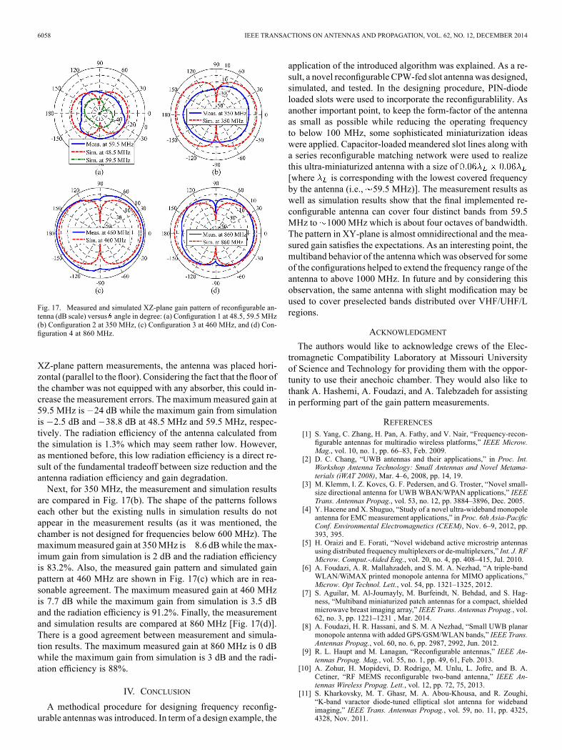
6058 IEEE TRANSACTIONS ON ANTENNAS AND PROPAGATION, VOL. 62, NO. 12, DECEMBER 2014
Fig. 17. Measured and simulated XZ-plane gain pattern of reconfigurable an-tenna (dB scale) versus angle in degree: (a) Configuration 1 at 48.5, 59.5 MHz(b) Configuration 2 at 350 MHz, (c) Configuration 3 at 460 MHz, and (d) Con-figuration 4 at 860 MHz.
XZ-plane pattern measurements, the antenna was placed hori-zontal (parallel to the floor). Considering the fact that the floor ofthe chamber was not equipped with any absorber, this could in-crease the measurement errors. The maximum measured gain at59.5 MHz is 24 dB while the maximum gain from simulationis 2.5 dB and 38.8 dB at 48.5 MHz and 59.5 MHz, respec-tively. The radiation efficiency of the antenna calculated fromthe simulation is 1.3% which may seem rather low. However,as mentioned before, this low radiation efficiency is a direct re-sult of the fundamental tradeoff between size reduction and theantenna radiation efficiency and gain degradation.Next, for 350 MHz, the measurement and simulation results
are compared in Fig. 17(b). The shape of the patterns followseach other but the existing nulls in simulation results do notappear in the measurement results (as it was mentioned, thechamber is not designed for frequencies below 600 MHz). Themaximummeasured gain at 350MHz is 8.6 dBwhile the max-imum gain from simulation is 2 dB and the radiation efficiencyis 83.2%. Also, the measured gain pattern and simulated gainpattern at 460 MHz are shown in Fig. 17(c) which are in rea-sonable agreement. The maximum measured gain at 460 MHzis 7.7 dB while the maximum gain from simulation is 3.5 dBand the radiation efficiency is 91.2%. Finally, the measurementand simulation results are compared at 860 MHz [Fig. 17(d)].There is a good agreement between measurement and simula-tion results. The maximum measured gain at 860 MHz is 0 dBwhile the maximum gain from simulation is 3 dB and the radi-ation efficiency is 88%.
IV. CONCLUSION
A methodical procedure for designing frequency reconfig-urable antennas was introduced. In term of a design example, the
application of the introduced algorithm was explained. As a re-sult, a novel reconfigurable CPW-fed slot antennawas designed,simulated, and tested. In the designing procedure, PIN-diodeloaded slots were used to incorporate the reconfigurablility. Asanother important point, to keep the form-factor of the antennaas small as possible while reducing the operating frequencyto below 100 MHz, some sophisticated miniaturization ideaswere applied. Capacitor-loaded meandered slot lines along witha series reconfigurable matching network were used to realizethis ultra-miniaturized antenna with a size of[where is corresponding with the lowest covered frequencyby the antenna (i.e., 59.5 MHz)]. The measurement results aswell as simulation results show that the final implemented re-configurable antenna can cover four distinct bands from 59.5MHz to 1000 MHz which is about four octaves of bandwidth.The pattern in XY-plane is almost omnidirectional and the mea-sured gain satisfies the expectations. As an interesting point, themultiband behavior of the antenna which was observed for someof the configurations helped to extend the frequency range of theantenna to above 1000 MHz. In future and by considering thisobservation, the same antenna with slight modification may beused to cover preselected bands distributed over VHF/UHF/Lregions.
ACKNOWLEDGMENT
The authors would like to acknowledge crews of the Elec-tromagnetic Compatibility Laboratory at Missouri Universityof Science and Technology for providing them with the oppor-tunity to use their anechoic chamber. They would also like tothank A. Hashemi, A. Foudazi, and A. Talebzadeh for assistingin performing part of the gain pattern measurements.
REFERENCES[1] S. Yang, C. Zhang, H. Pan, A. Fathy, and V. Nair, “Frequency-recon-
figurable antennas for multiradio wireless platforms,” IEEE Microw.Mag., vol. 10, no. 1, pp. 66–83, Feb. 2009.
[2] D. C. Chang, “UWB antennas and their applications,” in Proc. Int.Workshop Antenna Technology: Small Antennas and Novel Metama-terials (iWAT 2008), Mar. 4–6, 2008, pp. 14, 19.
[3] M. Klemm, I. Z. Kovcs, G. F. Pedersen, and G. Troster, “Novel small-size directional antenna for UWB WBAN/WPAN applications,” IEEETrans. Antennas Propag., vol. 53, no. 12, pp. 3884–3896, Dec. 2005.
[4] Y. Hacene and X. Shuguo, “Study of a novel ultra-wideband monopoleantenna for EMCmeasurement applications,” in Proc. 6th Asia-PacificConf. Environmental Electromagnetics (CEEM), Nov. 6–9, 2012, pp.393, 395.
[5] H. Oraizi and E. Forati, “Novel wideband active microstrip antennasusing distributed frequency multiplexers or de-multiplexers,” Int. J. RFMicrow. Comput.-Aided Eng., vol. 20, no. 4, pp. 408–415, Jul. 2010.
[6] A. Foudazi, A. R. Mallahzadeh, and S. M. A. Nezhad, “A triple-bandWLAN/WiMAX printed monopole antenna for MIMO applications,”Microw. Opt Technol. Lett., vol. 54, pp. 1321–1325, 2012.
[7] S. Aguilar, M. Al-Joumayly, M. Burfeindt, N. Behdad, and S. Hag-ness, “Multiband miniaturized patch antennas for a compact, shieldedmicrowave breast imaging array,” IEEE Trans. Antennas Propag., vol.62, no. 3, pp. 1221–1231 , Mar. 2014.
[8] A. Foudazi, H. R. Hassani, and S. M. A Nezhad, “Small UWB planarmonopole antenna with added GPS/GSM/WLAN bands,” IEEE Trans.Antennas Propag., vol. 60, no. 6, pp. 2987, 2992, Jun. 2012.
[9] R. L. Haupt and M. Lanagan, “Reconfigurable antennas,” IEEE An-tennas Propag. Mag., vol. 55, no. 1, pp. 49, 61, Feb. 2013.
[10] A. Zohur, H. Mopidevi, D. Rodrigo, M. Unlu, L. Jofre, and B. A.Cetiner, “RF MEMS reconfigurable two-band antenna,” IEEE An-tennas Wireless Propag. Lett., vol. 12, pp. 72, 75, 2013.
[11] S. Kharkovsky, M. T. Ghasr, M. A. Abou-Khousa, and R. Zoughi,“K-band varactor diode-tuned elliptical slot antenna for widebandimaging,” IEEE Trans. Antennas Propag., vol. 59, no. 11, pp. 4325,4328, Nov. 2011.

FALLAHPOUR et al.: MINIATURIZED RECONFIGURABLE MULTIBAND ANTENNA FOR MULTIRADIO WIRELESS COMMUNICATION 6059
[12] F. Yang and Y. Rahmat-Samii, “A reconfigurable patch antenna usingswitchable slots for circular polarization diversity,” IEEE Microw.Wireless Compon. Lett., vol. 12, no. 3, pp. 96–98, Mar. 2002.
[13] A. C. K. Mak, C. R. Rowell, R. D. Murch, and C. L. Mak, “Recon-figurable multiband antenna designs for wireless communication de-vices,” IEEE Trans. Antennas Propag., vol. 55, no. 7, pp. 1919–1928,Jul. 2007.
[14] N. Behdad and K. Sarabandi, “A varactor-tuned dual-band slot an-tenna,” IEEE Trans. Antennas Propag., vol. 54, no. 2, pp. 401–408,Feb. 2006.
[15] M. Fallahpour, M. Ghasr, and R. Zoughi, “A multiband reconfigurableCPW-fed slot antenna,” presented at the 2012 IEEE Int. Symp.Antennas and Propagation and USNC/URSI National Radio Science,Chicago, IL, USA, Jul. 8–13, 2012.
[16] G. Ruvio, M. J. Ammann, and Z. N. Chen, “Wideband reconfigurablerolled planar monopole antenna,” IEEE Trans. Antennas Propag., vol.55, no. 6, pp. 1760–1767, Jun. 2007.
[17] B. A. Cetiner, G. R. Crusats, L. Jofre, and N. Biyikli, “RF MEMS in-tegrated frequency reconfigurable annular slot antenna,” IEEE Trans.Antennas Propag., vol. 58, no. 3, pp. 626–632, Mar. 2010.
[18] I. A. Osaretin, A. Torres, A. , and C. C. Chen, “A novel compactdual-linear polarized UWB antenna for VHF/UHF applications,” IEEEAntennas Wireless Propag. Lett., vol. 8, pp. 145, 148, 2009.
[19] C. A. Balanis, Antenna Theory: Analysis And Design, 2nd ed. NewYork, NY, USA: Wiley, 1997.
[20] [Online]. Available: https://www.cst.com/[21] [Online]. Available: http://www.ansys.com/[22] [Online]. Available: http://interoperability.nj.gov/spectrum/
pubsaf_currfutneeds.pdf[23] H. D. Chen, “Broadband CPW-fed square slot antennas with a
widened tuning stub,” IEEE Trans. Antennas Propag., vol. 51, no. 8,pp. 1982–1986, Aug. 2003.
[24] D. M. Pozar, Microwave Engineering, 2nd ed. New York, NY, USA:Wiley, 1998.
[25] P. L. Chi, R. Waterhouse, and T. Itoh, “Antenna miniaturization usingslow wave enhancement factor from loaded transmission line models,”IEEE Trans. Antennas Propag., vol. 59, no. 1, pp. 48, 57, Jan. 2011.
[26] R. Azadegan and K. Sarabandi, “A novel approach for miniaturizationof slot antennas,” IEEE Trans. Antennas Propag., vol. 51, no. 3, pp.421–429, Mar. 2003.
[27] Microsemi, GC4200 Series PIN Diodes, Specification Sheet.[28] C. Wu, T. Wang, A. Ren, and D. G. Michelson, “Implementation of
reconfigurable patch antennas using reed switches,” IEEE AntennasWireless Propag. Lett., vol. 10, pp. 1023, 1026, 2011.
[29] [Online]. Available: http://www.ni.com/dataacquisition/nidaqmx[30] A. Grau, J. Romeu, L. Jofre, and F. De Flaviis, “A software defined
MEMS-reconfigurable PIXEL-antenna for narrowband MIMO sys-tems,” in Proc. Conf. Adaptive Hardware and Systems (AHS ’08.NASA/ESA), Jun. 22–25, 2008, pp. 141, 146.
[31] H. A. Wheeler, “Fundamental limitations of small antennas,” Proc.IRE, vol. 35, pp. 1479–1484, 1947.
[32] L. J. Chu, “Physical limitations of omnidirectional antennas,” J. Appl.Phys., vol. 19, pp. 1163–1175, 1948.
Mojtaba Fallahpour (S’09–M’13) received theB.Sc. and M.Sc. degrees in electrical engineeringfrom the Iran University of Science and Technology(IUST), Tehran, Iran, in 2005 and 2008, respec-tively. He completed the Ph.D. degree in 2013 atthe Missouri University of Science and Technology,formerly University of Missouri-Rolla (UMR), inelectrical engineering with an emphasis on electro-magnetics, radar, antenna, and microwave imaging.He has worked in signal integrity group in Micron
Technology, Inc. and hardware group in Cisco Sys-tems, Inc. as an intern from June to December 2012. Currently, he is a Postdoc-toral Research Associate with the University of Illinois at Urbana-Champaign.His research interests include development of fast numerical algorithms formultiscale multiphysics problems, inverse scattering, synthetic aperture radar,remote sensing, microwave nondestructive testing, microwave and terahertz
imaging, signal integrity, array antennas, optimization techniques, and minia-turized wideband reconfigurable antennas.Dr. Fallahpour is a member of Eta Kappa Nu and he was honored with the
American Society for Nondestructive Testing Graduate Fellowship Award(2009). He has also been recognized as outstanding reviewer by IEEETRANSACTIONS ON INSTRUMENTATION AND MEASUREMENTS (2013).
Mohammad Tayeb Ghasr (S’01–M’10–SM’12)received the B.S. degree in electrical engineeringdegree (magna cum laude) from the AmericanUniversity of Sharjah (AUS), Sharjah, United ArabEmirates, in 2002 and the M.S. degree in electricalengineering from the University of Missouri-Rolla,Rolla, in 2004, and the Ph.D. degree in electricalengineering from Missouri University of Scienceand Technology (Missouri S&T), Rolla, MO, USA,in 2009.Currently, he is an Assistant Research Professor
with the Applied Microwave Nondestructive Testing Laboratory (amntl), Elec-trical and Computer Engineering Department, Missouri University of Scienceand Technology (Missouri S&T). He has more than 90 journal papers, confer-ence proceedings and presentations, and technical reports. He has nine awardedand pending patents to his credit. His research interests include microwave andmillimeter-wave instrumentation and measurement, RF circuits, antennas, andnumerical electromagnetic analysis.Dr. Ghasr was a recipient of the 2013 I&M Outstanding Young Engineer
Award from the IEEE Instrumentation and Measurement Society, and the 2013H. A. Wheeler Prize Paper Award of the IEEE Antennas and Propagation So-ciety.
R. Zoughi (S’85–M’86–SM’93–F’06) received theB.S.E.E, M.S.E.E, and Ph.D. degrees in electricalengineering (radar remote sensing, radar systems,and microwaves) from the University of Kansas,Lawrence, KS, USA,He was with the Radar Systems and Remote
Sensing Laboratory (RSL) from 1981 until 1987.Currently, he is the Schlumberger Endowed Pro-fessor of Electrical and Computer Engineering atMissouri University of Science and Technology(Missouri S&T), formerly University of Mis-
souri-Rolla (UMR), Rolla, MO. Prior to joining Missouri S&T in January2001 and since 1987 he was with the Electrical and Computer EngineeringDepartment at Colorado State University (CSU), Fort Collins, CO, USA, wherehe was a Professor and established the Applied Microwave NondestructiveTesting Laboratory (amntl) (http://amntl.mst.edu/). He held the position ofBusiness Challenge Endowed Professor of Electrical and Computer Engi-neering from 1995 to 1997 while at CSU. He served as the Editor-in-Chiefof the IEEE TRANSACTIONS ON INSTRUMENTATION AND MEASUREMENT,from 2007 through 2011, two terms as an at-large AdCom member of theIEEE Instrumentation and Measurement (I&M) Society, currently serves asthe society’s President and an I&M Society Distinguished Lecturer. He isthe author of the textbook Microwave Nondestructive Testing and EvaluationPrinciples (Kluwer Academic: Dordrecht, the Netherlands, 2000), and theco-author of a chapter on Microwave Techniques in the book NondestructiveEvaluation: Theory, Techniques, and Applications (Marcel Dekker: New York,NY, USA, 2002).Dr. Zoughi has been the recipient of numerous teaching awards both at CSU
and Missouri S&T. He is the recipient of the 2007 IEEE Instrumentation andMeasurement Society Distinguished Service Award, the 2009 American Societyfor Nondestructive Testing (ASNT) Research Award for Sustained Excellenceand the 2011 IEEE Joseph F. Keithley Award in Instrumentation and Measure-ment. He served as the General Co-Chair of the 2013 IEEE Instrumentation andMeasurement Technology Conference (I2MTC). He is the co-author of over 541journal papers, conference proceedings and presentations and technical reports.He has thirteen patents to his credit all in the field of microwave nondestructivetesting and evaluation. He is also a Fellow of the American Society for Nonde-structive Testing.


