Embed Size (px)
Citation preview
PCIe-FRM24_B Users Manual (Rev 1.1)
-1- http://www.daqsystem.com
PCIe-FRM24_B User’s Manual
Windows, Windows2000, Windows NT and Windows XP are trademarks of Microsoft. We acknowledge that the
trademarks or service names of all other organizations mentioned in this document as their own property.
Information furnished by DAQ system is believed to be accurate and reliable. However, no responsibility is assumed by DAQ
system for its use, nor for any infringements of patents or other rights of third parties which may result from its use. No license is
granted by implication or otherwise under any patent or copyrights of DAQ system.
The information in this document is subject to change without notice and no part of this document may be copied or
reproduced without the prior written consent.
Copyrights 2005 DAQ system, All rights reserved.
PCIe-FRM24_B Users Manual (Rev 1.1)
-2- http://www.daqsystem.com
-- Contents --
1. Introduction
2. PCIe-FRM24 Functions
2.1 FPGA Block Diagram
2.2 Camera Link
2.3 Camera Link and PCIe-FRM24_B
2.4 Camera Link Cable
2.5 Encoder Trigger Controller
3. PCIe-FRM24 Board Description
3.1 PCB Layout
3.2 Description of the functional blocks
3.3 Connector Pin-out
3.3.1 J1 Connector
3.3.2 J2 Connector
3.3.3 J3 Connector
3.3.4 J4(MDR26) Connector
3.3.5 J5 Connector
3.3.6 J6(MDR26) Connector
3.3.7 J7 Connector
4. Installation
4.1 Hardware Installation
4.1.1 Package Contents
4.1.2 Installation Sequence
4.2 Software Driver Installation
5. Sample Program
5.1 FrmTest
Appendix
A.1 General Specification
A.2 Physical Dimension
Reference
PCIe-FRM24_B Users Manual (Rev 1.1)
-3- http://www.daqsystem.com
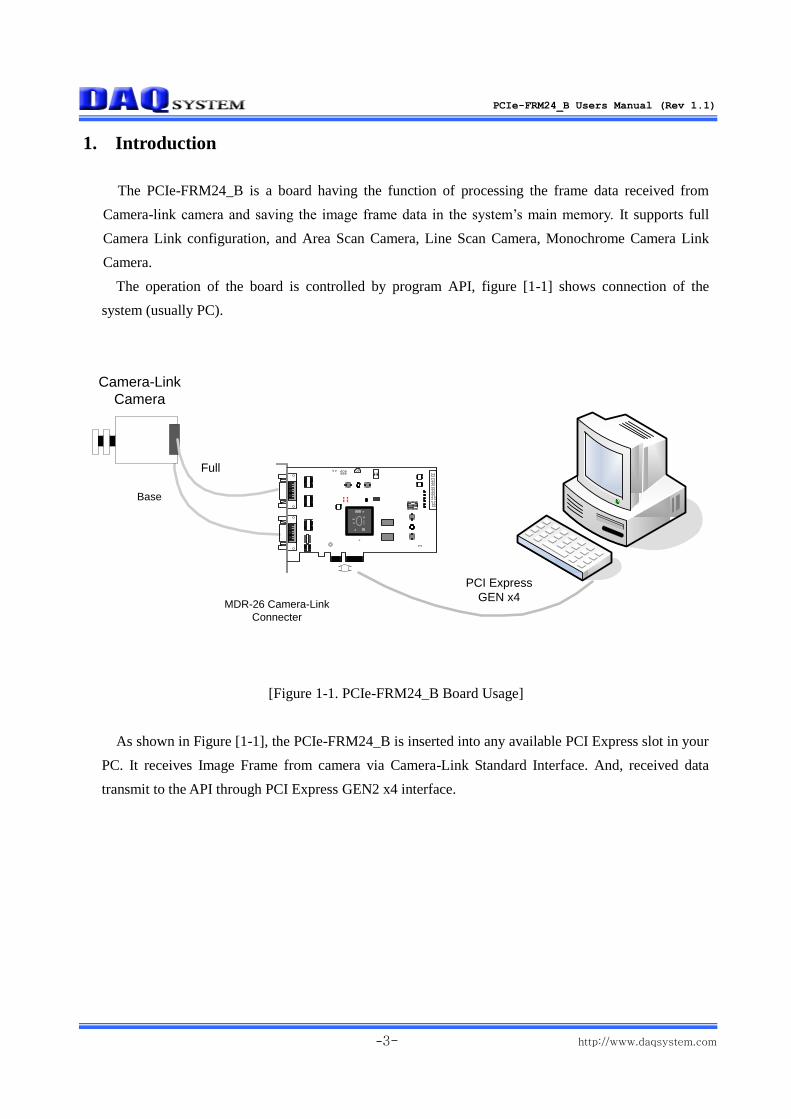
1. Introduction
The PCIe-FRM24_B is a board having the function of processing the frame data received from
Camera-link camera and saving the image frame data in the system’s main memory. It supports full
Camera Link configuration, and Area Scan Camera, Line Scan Camera, Monochrome Camera Link
Camera.
The operation of the board is controlled by program API, figure [1-1] shows connection of the
system (usually PC).
Camera-Link
Camera
Full
PCI Express
GEN x4MDR-26 Camera-Link
Connecter
Base
[Figure 1-1. PCIe-FRM24_B Board Usage]
As shown in Figure [1-1], the PCIe-FRM24_B is inserted into any available PCI Express slot in your
PC. It receives Image Frame from camera via Camera-Link Standard Interface. And, received data
transmit to the API through PCI Express GEN2 x4 interface.
PCIe-FRM24_B Users Manual (Rev 1.1)
-4- http://www.daqsystem.com
[Features of the PCIe-FRM24]
Support Base Configuration Camera Link
Support Full/Medium Configuration Camera Link
Support Line Scan & Area Scan Camera
PCI Express GEN2 4x Interface
Acquisition pixel clock rates up to 85MHz
Data rate of up to maximum 2Gbytes/sec (GEN2)
UART(Data bit 8, 1 start, 1 stop, No parity, 9600/19200/38400/57600/115200bps) Rx/Tx
External Device Interface : 4 TTL Digital Input/Output, and 2 TTL trigger Input Signals
and 4-pair RS-422
User Environment : Windows 2000 SP4, Windows XP SP1
Convenient Windows Application Programming Interface(DLL)
[Application]
Image Acquisition (Pattern, Particle etc.)
Inspection Equipment (Sensor, Semiconductor, Device etc.)
Security Solution
Black and White, Color Image Display
Medical Image Capture (X-ray, Supersonic etc.)
PCIe-FRM24_B Users Manual (Rev 1.1)
-5- http://www.daqsystem.com
2. PCIe-FRM24_B Functions
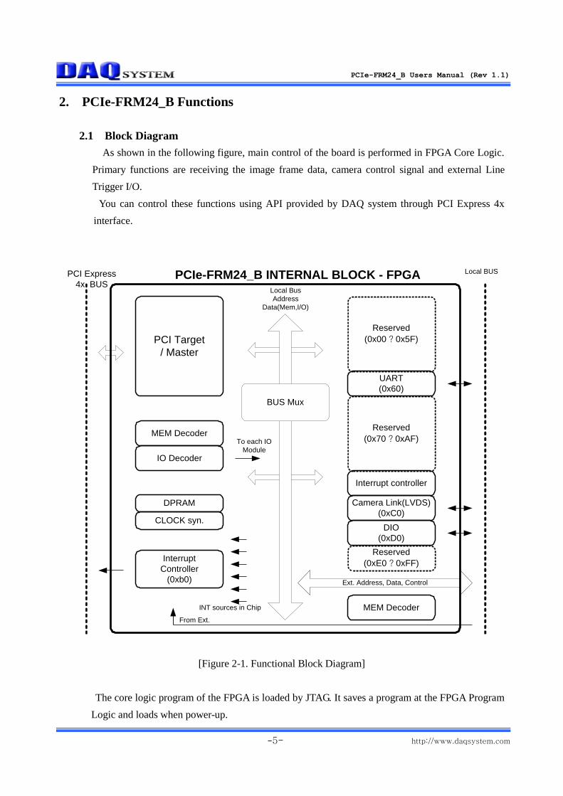
2.1 Block Diagram
As shown in the following figure, main control of the board is performed in FPGA Core Logic.
Primary functions are receiving the image frame data, camera control signal and external Line
Trigger I/O.
You can control these functions using API provided by DAQ system through PCI Express 4x
interface.
PCI Target
/ Master
PCI Express
4x BUSLocal Bus
Address
Data(Mem,I/O)
Reserved
(0x00 ? 0x5F)
Reserved
(0x70 ? 0xAF)
UART
(0x60)
Camera Link(LVDS)
(0xC0)
Interrupt controller
DIO
(0xD0)
Ext. Address, Data, Control
Local BUS
Interrupt
Controller
(0xb0)
INT sources in Chip
IO Decoder
MEM Decoder
To each IO
Module
PCIe-FRM24_B INTERNAL BLOCK - FPGA
DPRAM
From Ext.
CLOCK syn.
MEM Decoder
BUS Mux
Reserved
(0xE0 ? 0xFF)
[Figure 2-1. Functional Block Diagram]
The core logic program of the FPGA is loaded by JTAG. It saves a program at the FPGA Program
Logic and loads when power-up.
PCIe-FRM24_B Users Manual (Rev 1.1)
-6- http://www.daqsystem.com
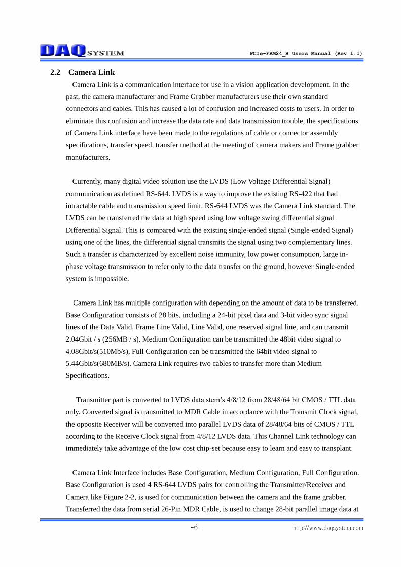
2.2 Camera Link
Camera Link is a communication interface for use in a vision application development. In the
past, the camera manufacturer and Frame Grabber manufacturers use their own standard
connectors and cables. This has caused a lot of confusion and increased costs to users. In order to
eliminate this confusion and increase the data rate and data transmission trouble, the specifications
of Camera Link interface have been made to the regulations of cable or connector assembly
specifications, transfer speed, transfer method at the meeting of camera makers and Frame grabber
manufacturers.
Currently, many digital video solution use the LVDS (Low Voltage Differential Signal)
communication as defined RS-644. LVDS is a way to improve the existing RS-422 that had
intractable cable and transmission speed limit. RS-644 LVDS was the Camera Link standard. The
LVDS can be transferred the data at high speed using low voltage swing differential signal
Differential Signal. This is compared with the existing single-ended signal (Single-ended Signal)
using one of the lines, the differential signal transmits the signal using two complementary lines.
Such a transfer is characterized by excellent noise immunity, low power consumption, large in-
phase voltage transmission to refer only to the data transfer on the ground, however Single-ended
system is impossible.
Camera Link has multiple configuration with depending on the amount of data to be transferred.
Base Configuration consists of 28 bits, including a 24-bit pixel data and 3-bit video sync signal
lines of the Data Valid, Frame Line Valid, Line Valid, one reserved signal line, and can transmit
2.04Gbit / s (256MB / s). Medium Configuration can be transmitted the 48bit video signal to
4.08Gbit/s(510Mb/s), Full Configuration can be transmitted the 64bit video signal to
5.44Gbit/s(680MB/s). Camera Link requires two cables to transfer more than Medium
Specifications.
Transmitter part is converted to LVDS data stem’s 4/8/12 from 28/48/64 bit CMOS / TTL data
only. Converted signal is transmitted to MDR Cable in accordance with the Transmit Clock signal,
the opposite Receiver will be converted into parallel LVDS data of 28/48/64 bits of CMOS / TTL
according to the Receive Clock signal from 4/8/12 LVDS data. This Channel Link technology can
immediately take advantage of the low cost chip-set because easy to learn and easy to transplant.
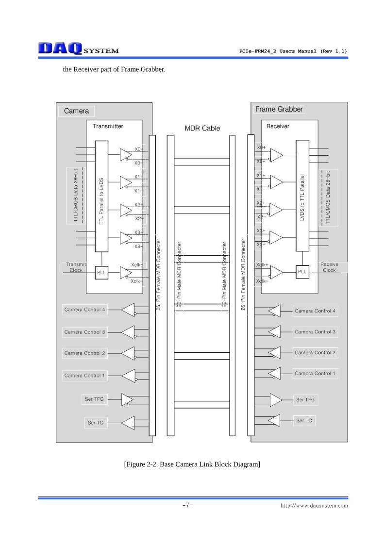
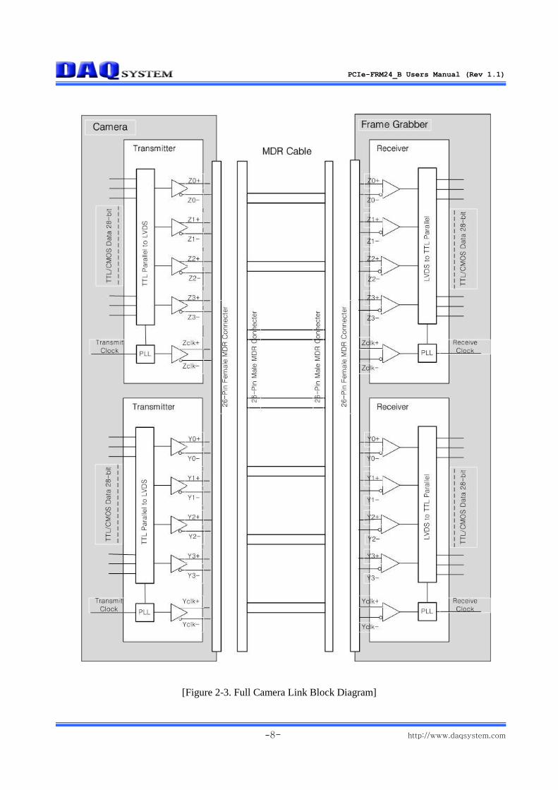
Camera Link Interface includes Base Configuration, Medium Configuration, Full Configuration.
Base Configuration is used 4 RS-644 LVDS pairs for controlling the Transmitter/Receiver and
Camera like Figure 2-2, is used for communication between the camera and the frame grabber.
Transferred the data from serial 26-Pin MDR Cable, is used to change 28-bit parallel image data at
PCIe-FRM24_B Users Manual (Rev 1.1)
-7- http://www.daqsystem.com
the Receiver part of Frame Grabber.
[Figure 2-2. Base Camera Link Block Diagram]
PCIe-FRM24_B Users Manual (Rev 1.1)
-8- http://www.daqsystem.com
[Figure 2-3. Full Camera Link Block Diagram]
PCIe-FRM24_B Users Manual (Rev 1.1)
-9- http://www.daqsystem.com
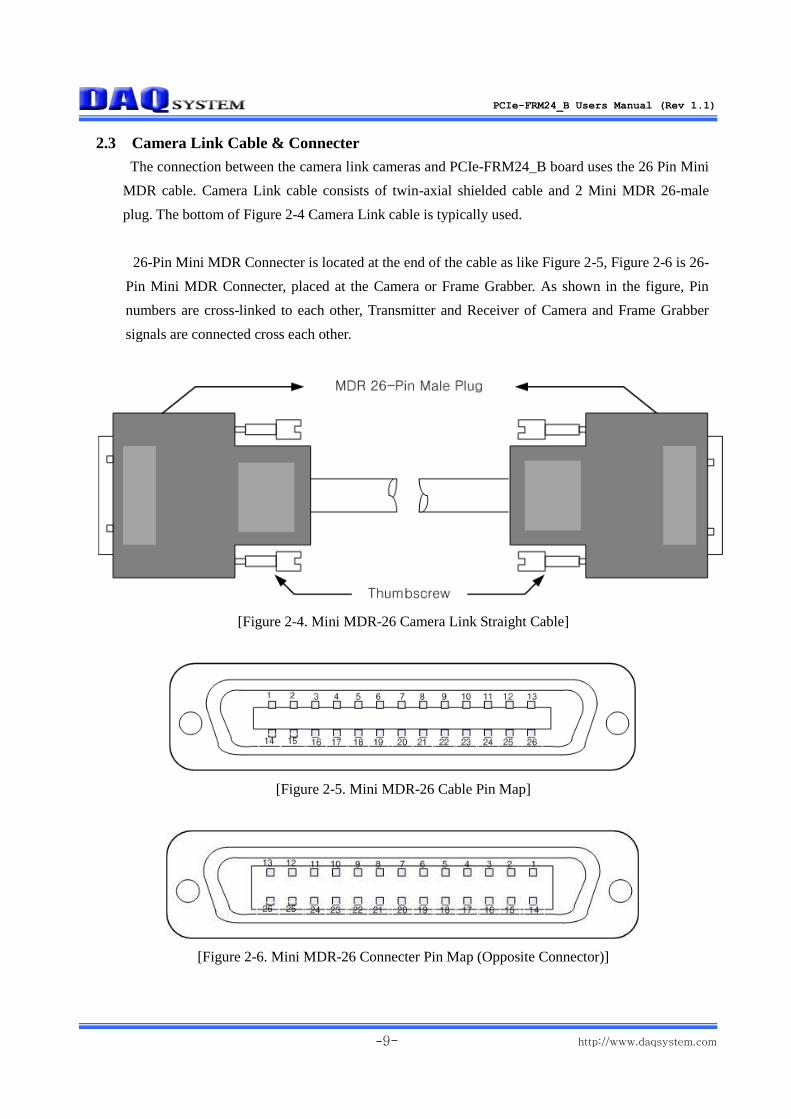
2.3 Camera Link Cable & Connecter
The connection between the camera link cameras and PCIe-FRM24_B board uses the 26 Pin Mini
MDR cable. Camera Link cable consists of twin-axial shielded cable and 2 Mini MDR 26-male
plug. The bottom of Figure 2-4 Camera Link cable is typically used.
26-Pin Mini MDR Connecter is located at the end of the cable as like Figure 2-5, Figure 2-6 is 26-
Pin Mini MDR Connecter, placed at the Camera or Frame Grabber. As shown in the figure, Pin
numbers are cross-linked to each other, Transmitter and Receiver of Camera and Frame Grabber
signals are connected cross each other.
[Figure 2-4. Mini MDR-26 Camera Link Straight Cable]
[Figure 2-5. Mini MDR-26 Cable Pin Map]
[Figure 2-6. Mini MDR-26 Connecter Pin Map (Opposite Connector)]
PCIe-FRM24_B Users Manual (Rev 1.1)
-10- http://www.daqsystem.com
Cable Specification (Standard)
Characteristic Impedance : 100 ±10 ohms
Propagation Delay : 1.5 NS/ft
Mutal Capacitance : 17 pF/ft nominal
Conductor Resistance : 72 Ohms / 1k
Velocity of Propagation : 78% maximum
Voltage Rating : 30V
Temperature : -20 ~ +80℃
Length (m) : 1 / 2 / 3 / 4.5 / 5 / 7 / 10
2.4 Camera Link and PCIe-FRM24_B
PCIe-FRM24_B supports Camera Link Base/Medium/Full Configuration. Base Configuration,
24 data bits and four enable signals Frame Valid, Line Valid, Data Valid and a spare, including 28-
bit parallel signals serialized four LVDS signal lines and one LVDS signal line to fit the camera
and synchronous LVDS signal lines including four CC (Camera Control) signal and full 11
includes two asynchronous serial communication to communicate with the camera LVDS lines, is
transmitted through one MDR cable. In order to use the MDR Medium / Full Configuration is
used other cable and has a total 64bit wide video path.
The transmitted signal is parallelized to 64-bit parallel image signal and Frame Valid, Line Valid,
Data Valid, and a spare for each specification from 12 image LVDS serial signal through channel
link chip of PCIe-FRM24_B.
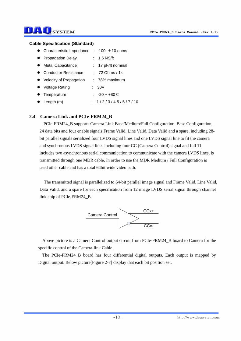
CCx+
CCx-
Camera Control
Above picture is a Camera Control output circuit from PCIe-FRM24_B board to Camera for the
specific control of the Camera-link Cable.
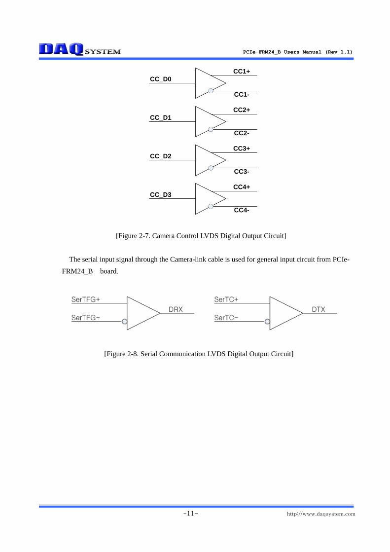
The PCIe-FRM24_B board has four differential digital outputs. Each output is mapped by
Digital output. Below picture[Figure 2-7] display that each bit position set.
PCIe-FRM24_B Users Manual (Rev 1.1)
-11- http://www.daqsystem.com
CC1+
CC1-
CC_D0
CC2+
CC2-
CC_D1
CC3+
CC3-
CC_D2
CC4+
CC4-
CC_D3
[Figure 2-7. Camera Control LVDS Digital Output Circuit]
The serial input signal through the Camera-link cable is used for general input circuit from PCIe-
FRM24_B board.
[Figure 2-8. Serial Communication LVDS Digital Output Circuit]
PCIe-FRM24_B Users Manual (Rev 1.1)
-12- http://www.daqsystem.com
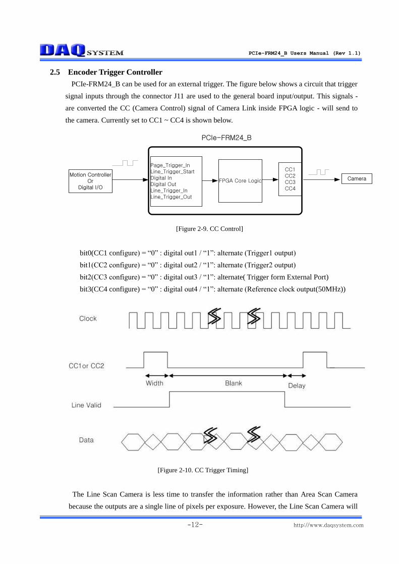
2.5 Encoder Trigger Controller
PCIe-FRM24_B can be used for an external trigger. The figure below shows a circuit that trigger
signal inputs through the connector J11 are used to the general board input/output. This signals -
are converted the CC (Camera Control) signal of Camera Link inside FPGA logic - will send to
the camera. Currently set to CC1 ~ CC4 is shown below.
PCIe-FRM24_B
CC1CC2CC3CC4
Page_Trigger_InLine_Trigger_StartDigital InDigital OutLine_Trigger_InLine_Trigger_Out
FPGA Core Logic CameraMotion Controller
OrDigital I/O
[Figure 2-9. CC Control]
bit0(CC1 configure) = “0” : digital out1 / “1”: alternate (Trigger1 output)
bit1(CC2 configure) = “0” : digital out2 / “1”: alternate (Trigger2 output)
bit2(CC3 configure) = “0” : digital out3 / “1”: alternate( Trigger form External Port)
bit3(CC4 configure) = “0” : digital out4 / “1”: alternate (Reference clock output(50MHz))
[Figure 2-10. CC Trigger Timing]
The Line Scan Camera is less time to transfer the information rather than Area Scan Camera
because the outputs are a single line of pixels per exposure. However, the Line Scan Camera will
PCIe-FRM24_B Users Manual (Rev 1.1)
-13- http://www.daqsystem.com
be required moving objects in order to obtain images. Synchronization between the movements
of the camera and the object is required. This synchronization is a little difference according to
the manufacture’s cameras and is performed by the trigger pulse which most of the triggering
signal of an external camera or the camera’s itself. The trigger pulse is initiated by the application.
A thickness, width, delay of the trigger can be gave a value (Blank, Width, Delay) by the program.
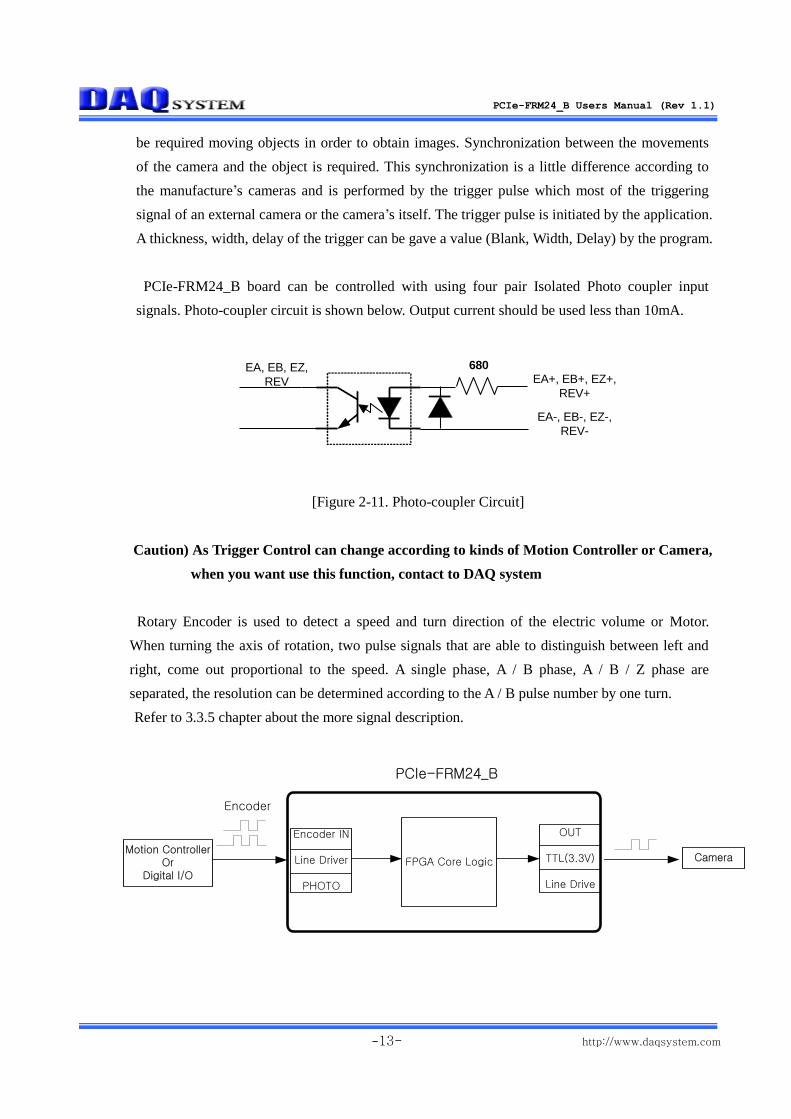
PCIe-FRM24_B board can be controlled with using four pair Isolated Photo coupler input
signals. Photo-coupler circuit is shown below. Output current should be used less than 10mA.
EA, EB, EZ,
REV EA+, EB+, EZ+,
REV+
EA-, EB-, EZ-,
REV-
680
[Figure 2-11. Photo-coupler Circuit]
Caution) As Trigger Control can change according to kinds of Motion Controller or Camera,
when you want use this function, contact to DAQ system
Rotary Encoder is used to detect a speed and turn direction of the electric volume or Motor.
When turning the axis of rotation, two pulse signals that are able to distinguish between left and
right, come out proportional to the speed. A single phase, A / B phase, A / B / Z phase are
separated, the resolution can be determined according to the A / B pulse number by one turn.
Refer to 3.3.5 chapter about the more signal description.
PCIe-FRM24_B
OUT
TTL(3.3V)
Line Drive
Encoder
Encoder IN
Line Driver
PHOTO
FPGA Core Logic CameraMotion Controller
OrDigital I/O
PCIe-FRM24_B Users Manual (Rev 1.1)
-14- http://www.daqsystem.com
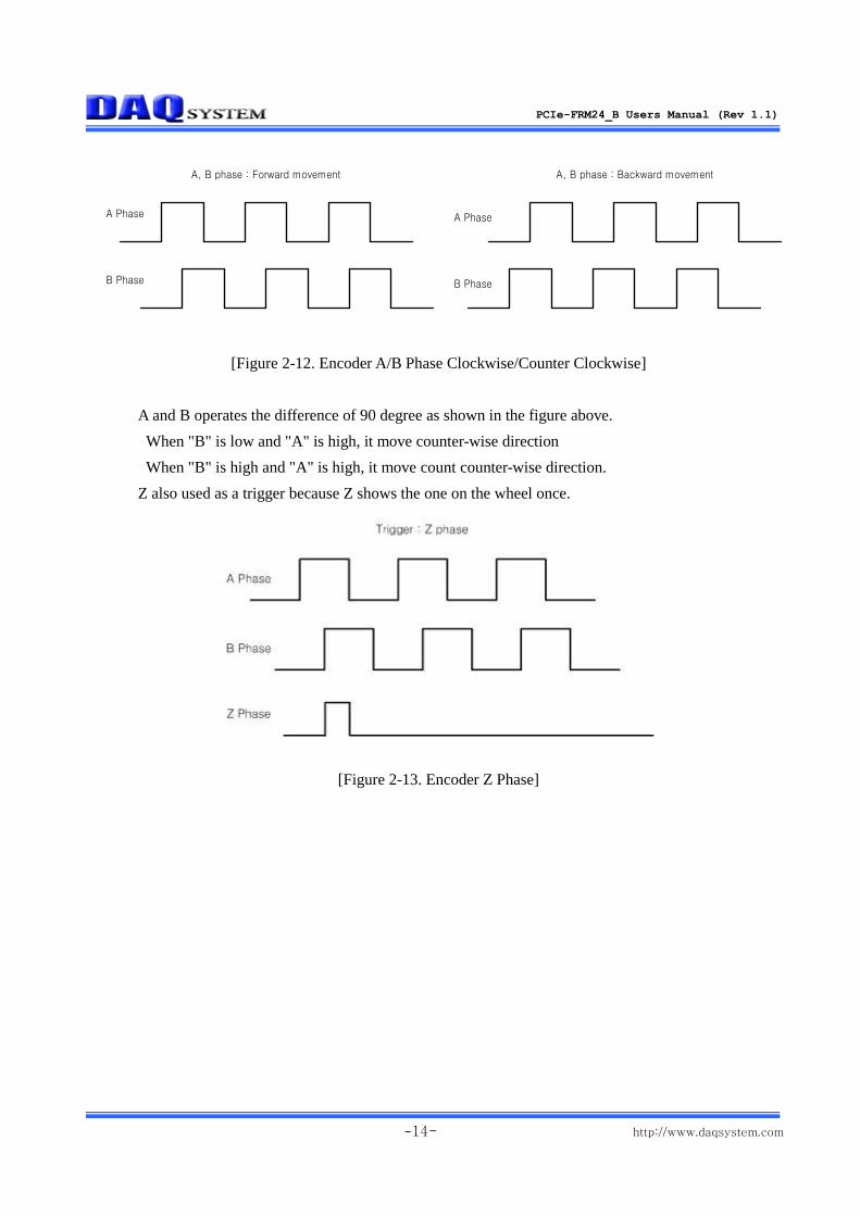
A, B phase : Forward movement A, B phase : Backward movement
A Phase
B Phase
A Phase
B Phase
[Figure 2-12. Encoder A/B Phase Clockwise/Counter Clockwise]
A and B operates the difference of 90 degree as shown in the figure above.
When "B" is low and "A" is high, it move counter-wise direction
When "B" is high and "A" is high, it move count counter-wise direction.
Z also used as a trigger because Z shows the one on the wheel once.
[Figure 2-13. Encoder Z Phase]
PCIe-FRM24_B Users Manual (Rev 1.1)
-15- http://www.daqsystem.com
3. PCIe-FRM24_B Board Description
In this chapter, the primary functions of the PCIe-FRM24 board are described briefly. For more
information, refer to the device specification
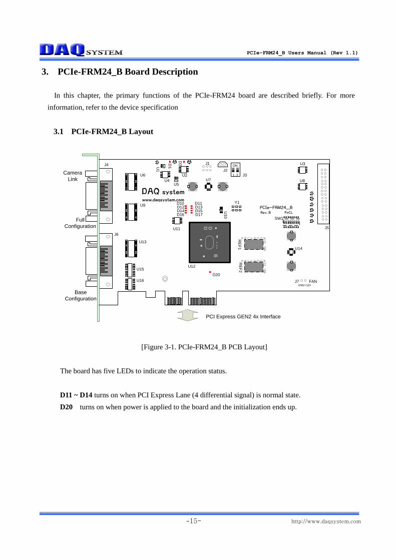
3.1 PCIe-FRM24_B Layout
Camera
Link
PCI Express GEN2 4x Interface
U13
U6
U12
U16
J2
U9
D20
U7
DAQ systemwww.daqsystem.com
PCIe-FRM24_B Rev. B PoCL
U15
U11 J5
ON
1 2 J3
J4
J6
Full
Configuration
Base
Configuration
D11D13D15D17
D10D12D14D16
123 7
89
ACEGJLNR
U3
U8
123 7
89
ACEGJLNR
U14
J7
J1
FANGND/+12V
Y1
U1
0
SW1
RE
F1
RE
F2
U1
U5
U2
U4
D1
D3
[Figure 3-1. PCIe-FRM24_B PCB Layout]
The board has five LEDs to indicate the operation status.
D11 ~ D14 turns on when PCI Express Lane (4 differential signal) is normal state.
D20 turns on when power is applied to the board and the initialization ends up.

PCIe-FRM24_B Users Manual (Rev 1.1)
-16- http://www.daqsystem.com
3.2 Description of the functional blocks
(1) MDR-26 Connecter : J4, J6
Camera Link Base (J6), medium/Full (J4) Signal Connector
(2) LVDS Link : U6, U9, U13
Receive Image frame
(3) FPGA : U12
All of the board functions are controlled by the Logic program of the FPGA.
(4) Line Trigger : J5
It is supposed to I/O circuit for external devices.
(5) Regulator : U7, U14
This block is for supplying the power to the board.
.
PCIe-FRM24_B Users Manual (Rev 1.1)
-17- http://www.daqsystem.com
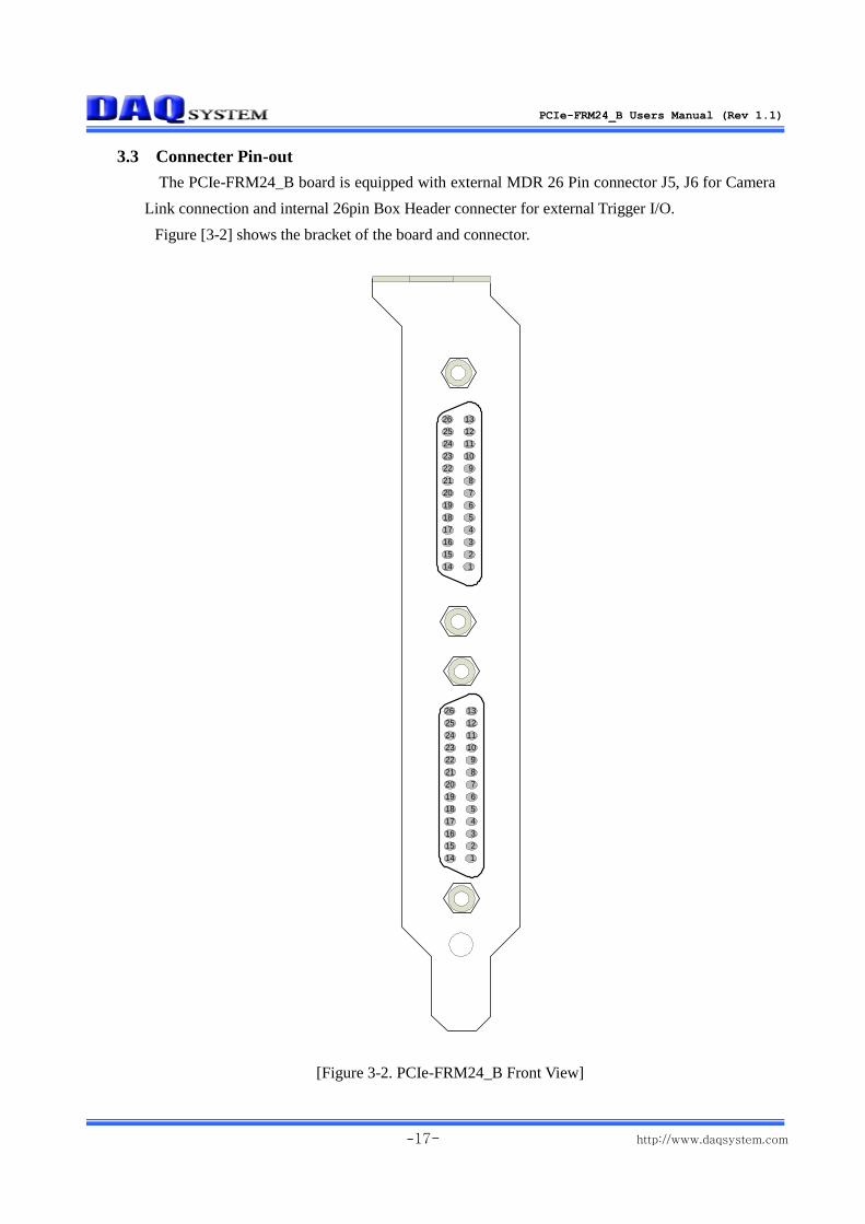
3.3 Connecter Pin-out
The PCIe-FRM24_B board is equipped with external MDR 26 Pin connector J5, J6 for Camera
Link connection and internal 26pin Box Header connecter for external Trigger I/O.
Figure [3-2] shows the bracket of the board and connector.
3
10
9
8
7
6
1
2
5
4
19
18
17
16
15
14
13
12
1124
23
22
21
20
26
25
3
10
9
8
7
6
1
2
5
4
19
18
17
16
15
14
13
12
1124
23
22
21
20
26
25
[Figure 3-2. PCIe-FRM24_B Front View]
PCIe-FRM24_B Users Manual (Rev 1.1)
-18- http://www.daqsystem.com
3.3.1 J1 jumper (2Pin Header, 2.54mm)
The J1 connector is used for the FPGA program upgrade. Never use it at the normal
operation. [Figure 3-6] shows the J9 connector.
3.3.2 J2 Connector
It is a 12V external DC power connector.
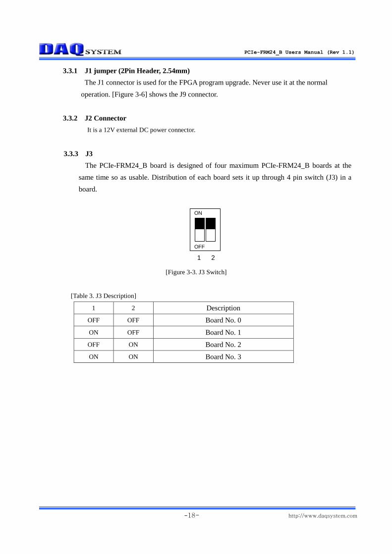
3.3.3 J3
The PCIe-FRM24_B board is designed of four maximum PCIe-FRM24_B boards at the
same time so as usable. Distribution of each board sets it up through 4 pin switch (J3) in a
board.
1
ON
OFF
2
[Figure 3-3. J3 Switch]
[Table 3. J3 Description]
1 2 Description
OFF OFF Board No. 0
ON OFF Board No. 1
OFF ON Board No. 2
ON ON Board No. 3
PCIe-FRM24_B Users Manual (Rev 1.1)
-19- http://www.daqsystem.com
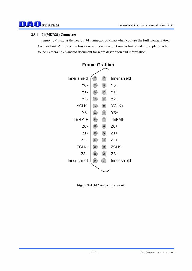
3.3.4 J4(MDR26) Connecter
Figure [3-4] shows the board’s J4 connector pin-map when you use the Full Configuration
Camera Link. All of the pin functions are based on the Camera link standard, so please refer
to the Camera link standard document for more description and information.
3
10
9
8
7
6
1
2
5
4
19
18
17
16
15
14
13
12
1124
23
22
21
20
Inner shield Inner shield
26
25
Z0-
TERMI+
YCLK-
Y3-
Y2-
Y1-
Y0-
Inner shield
Frame Grabber
Z0+
TERMI-
YCLK+
Y3+
Y2+
Y1+
Y0+
Inner shield
Z3+
ZCLK+
Z2+
Z1+
Z3-
ZCLK-
Z2-
Z1-
[Figure 3-4. J4 Connector Pin-out]
PCIe-FRM24_B Users Manual (Rev 1.1)
-20- http://www.daqsystem.com
[Table4. J4 Connecter Description]
Pin Signal Name Description Remark
1 Inner Shield Cable shield
2 Z3+- Camera link LVDS receive data11+
3 ZCLK+ Camera link LVDS receive clock+
4 Z2+- Camera link LVDS receive data10+
5 Z1- Camera link LVDS receive data9+
6 Z0+ Camera link LVDS receive data8+
7 TERMI- Serial to Camera-
8 Y3+ Camera link LVDS receive data7 +
9 YCLK+ Camera link LVDS receive clock +
10 Y2+ Camera link LVDS receive data6 +
11 Y1+ Camera link LVDS receive data5 +
12 Y0+ Camera link LVDS receive data4 +
13 Inner Shield
14 Inner Shield
15 Z3- Camera link LVDS receive data11-
16 ZCLK- Camera link LVDS receive clock-
17 Z2- Camera link LVDS receive data10-
18 Z1- Camera link LVDS receive data9-
19 Z0- Camera link LVDS receive data8-
20 TERMI+ Serial to Camera+
21 Y3- Camera link LVDS receive data7-
22 YCLK- Camera link LVDS receive clock-
23 Y2- Camera link LVDS receive data6-
24 Y1- Camera link LVDS receive data5-
25 Y0- Camera link LVDS receive data4-
26 Inner Shield
(Note) For more information, refer to Camera Link Standard Specification.
PCIe-FRM24_B Users Manual (Rev 1.1)
-21- http://www.daqsystem.com
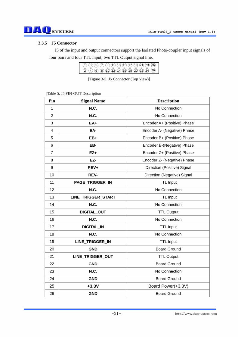
3.3.5 J5 Connector
J5 of the input and output connectors support the Isolated Photo-coupler input signals of
four pairs and four TTL Input, two TTL Output signal line.
1
2
3
4
95
6 8
7
10
11
12
13
14 20 24
2321
22
19
18
17
16
15
26
25
[Figure 3-5. J5 Connector (Top View)]
[Table 5. J5 PIN-OUT Description
Pin Signal Name Description
1 N.C. No Connection
2 N.C. No Connection
3 EA+ Encoder A+ (Positive) Phase
4 EA- Encoder A- (Negative) Phase
5 EB+ Encoder B+ (Positive) Phase
6 EB- Encoder B-(Negative) Phase
7 EZ+ Encoder Z+ (Positive) Phase
8 EZ- Encoder Z- (Negative) Phase
9 REV+ Direction (Positive) Signal
10 REV- Direction (Negative) Signal
11 PAGE_TRIGGER_IN TTL Input
12 N.C. No Connection
13 LINE_TRIGGER_START TTL Input
14 N.C. No Connection
15 DIGITAL_OUT TTL Output
16 N.C. No Connection
17 DIGITAL_IN TTL Input
18 N.C. No Connection
19 LINE_TRIGGER_IN TTL Input
20 GND Board Ground
21 LINE_TRIGGER_OUT TTL Output
22 GND Board Ground
23 N.C. No Connection
24 GND Board Ground
25 +3.3V Board Power(+3.3V)
26 GND Board Ground
PCIe-FRM24_B Users Manual (Rev 1.1)
-22- http://www.daqsystem.com
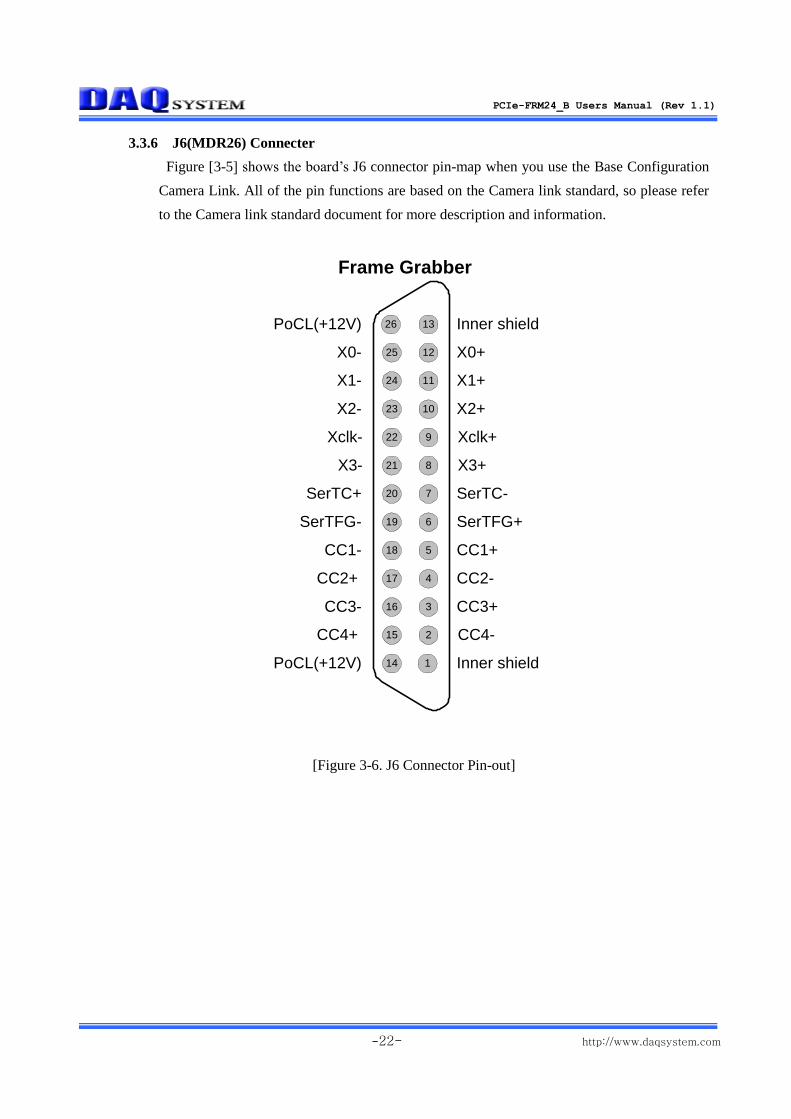
3.3.6 J6(MDR26) Connecter
Figure [3-5] shows the board’s J6 connector pin-map when you use the Base Configuration
Camera Link. All of the pin functions are based on the Camera link standard, so please refer
to the Camera link standard document for more description and information.
3
10
9
8
7
6
1
2
5
4
19
18
17
16
15
14
13
12
1124
23
22
21
20
PoCL(+12V) Inner shield
26
25
SerTFG-
SerTC+
Xclk-
X3-
X2-
X1-
X0-
PoCL(+12V)
Frame Grabber
SerTFG+
SerTC-
Xclk+
X3+
X2+
X1+
X0+
Inner shield
CC4-
CC3+
CC2-
CC1+
CC4+
CC3-
CC2+
CC1-
[Figure 3-6. J6 Connector Pin-out]
PCIe-FRM24_B Users Manual (Rev 1.1)
-23- http://www.daqsystem.com
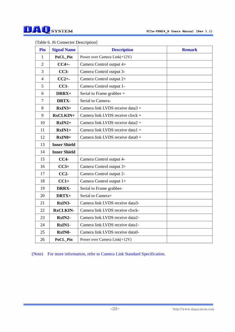
[Table 6. J6 Connecter Description]
Pin Signal Name Description Remark
1 PoCL_Pin Power over Camera Link(+12V)
2 CC4+- Camera Control output 4+
3 CC3- Camera Control output 3-
4 CC2+- Camera Control output 2+
5 CC1- Camera Control output 1-
6 DRRX+ Serial to Frame grabber +
7 DRTX- Serial to Camera-
8 RxIN3+ Camera link LVDS receive data3 +
9 RxCLKIN+ Camera link LVDS receive clock +
10 RxIN2+ Camera link LVDS receive data2 +
11 RxIN1+ Camera link LVDS receive data1 +
12 RxIN0+ Camera link LVDS receive data0 +
13 Inner Shield
14 Inner Shield
15 CC4- Camera Control output 4-
16 CC3+ Camera Control output 3+
17 CC2- Camera Control output 2-
18 CC1+ Camera Control output 1+
19 DRRX- Serial to Frame grabber-
20 DRTX+ Serial to Camera+
21 RxIN3- Camera link LVDS receive data3-
22 RxCLKIN- Camera link LVDS receive clock-
23 RxIN2- Camera link LVDS receive data2-
24 RxIN1- Camera link LVDS receive data1-
25 RxIN0- Camera link LVDS receive data0-
26 PoCL_Pin Power over Camera Link(+12V)
(Note) For more information, refer to Camera Link Standard Specification.
PCIe-FRM24_B Users Manual (Rev 1.1)
-24- http://www.daqsystem.com
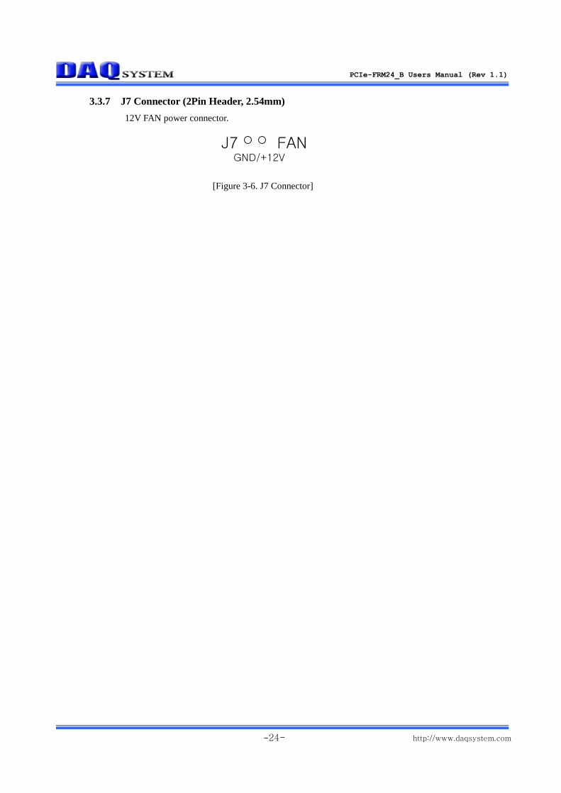
3.3.7 J7 Connector (2Pin Header, 2.54mm)
12V FAN power connector.
J7 FANGND/+12V
[Figure 3-6. J7 Connector]
PCIe-FRM24_B Users Manual (Rev 1.1)
-25- http://www.daqsystem.com
4. Installation
4.1 Hardware Installation
In addition to the user’s Manual, the package includes the following items. If any of these items
is missing or damaged, contact DAQ system.
After unpacking, inspect the board carton to make sure there are no damages on the board.
4.1.1 Package Contents
① PCIe-FRM24_B Board
② CD (Driver/Manual/API/Sample Source etc.)
- Document Folder : Manual and Catalog
- Driver Folder : pcie_frm24.sys, pcie-frm24.inf
- Sample Folder : Sample Application and DLL
- TestApp Folder : FrmTest.exe
4.1.2 Installation Process
① Turn off the PC power.
② Remove the computer cover using the instructions from the computer manual.
③ Insert the board empty PCI Express slot as soon as possible to close the CPU.
④ Remove the blank metal plate located at the back of the selected slot. Keep the removed
screw to fasten the board after installation.
⑤ You should try number 3 in case of multi-board.
PCIe-FRM24_B Users Manual (Rev 1.1)
-26- http://www.daqsystem.com
4.2 Software Driver Installation
To install your PCIe-FRM24_B board in your PC, follow the steps described in the document
“How to install PCI DAQ Board” provided by DAQ System. If the document is missing, you can
get it from www.daqsystem.com. The PCIe-FRM24_B board is completely Plug & Play. There
are no switches or jumpers to set. Therefore you can install it easily.
- Your OS requirement : Windows 2000 SP4 or Windows XP SP1 above
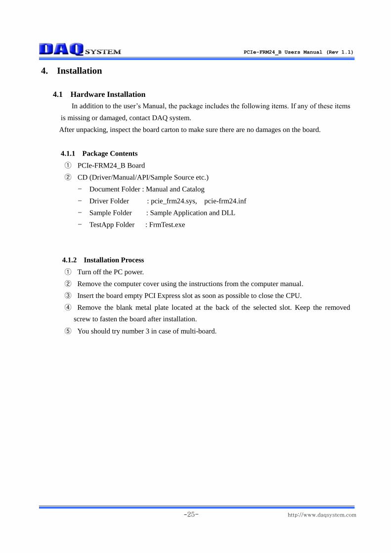
The PCIe-FRM24_B connects to Express Card Port. After that you can show the below picture
of “Welcome to found New Hardware Search Wizard” window.
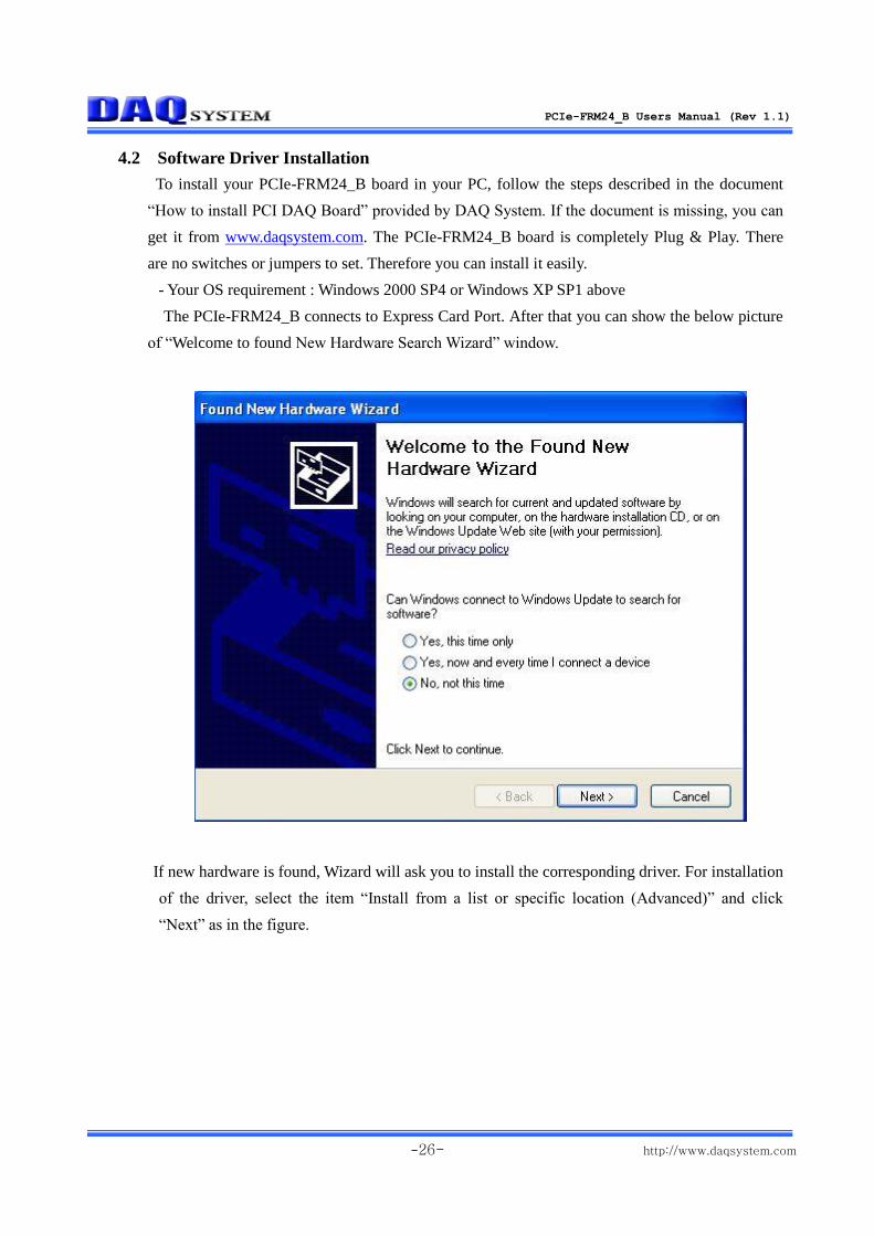
If new hardware is found, Wizard will ask you to install the corresponding driver. For installation
of the driver, select the item “Install from a list or specific location (Advanced)” and click
“Next” as in the figure.
PCIe-FRM24_B Users Manual (Rev 1.1)
-27- http://www.daqsystem.com
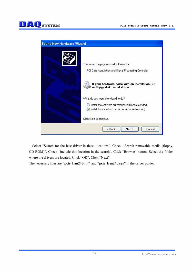
Select “Search for the best driver in these locations”. Check “Search removable media (floppy,
CD-ROM)”. Check “include this location in the search”. Click “Browse” button. Select the folder
where the drivers are located. Click “OK”. Click “Next”.
The necessary files are “pcie_frm24b.inf” and “pcie_frm24b.sys” in the driver polder.
PCIe-FRM24_B Users Manual (Rev 1.1)
-28- http://www.daqsystem.com
PCIe-FRM24_B Users Manual (Rev 1.1)
-29- http://www.daqsystem.com
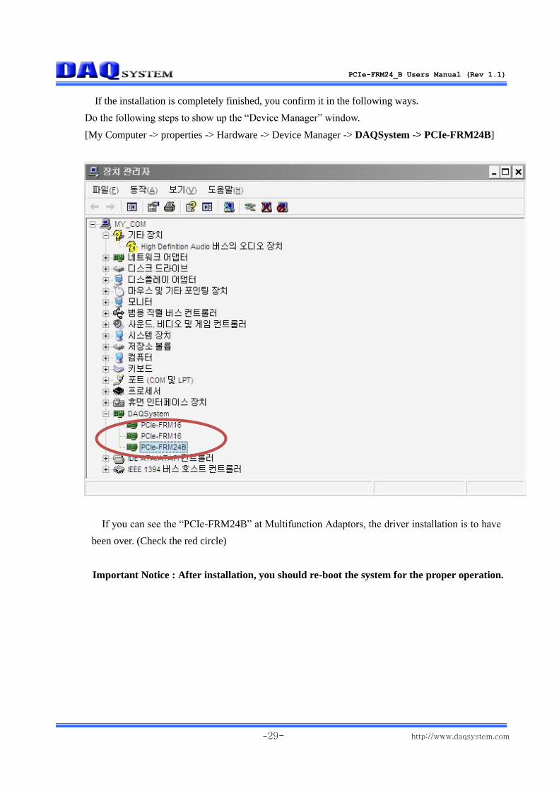
If the installation is completely finished, you confirm it in the following ways.
Do the following steps to show up the “Device Manager” window.
[My Computer -> properties -> Hardware -> Device Manager -> DAQSystem -> PCIe-FRM24B]
If you can see the “PCIe-FRM24B” at Multifunction Adaptors, the driver installation is to have
been over. (Check the red circle)
Important Notice : After installation, you should re-boot the system for the proper operation.
PCIe-FRM24_B Users Manual (Rev 1.1)
-30- http://www.daqsystem.com
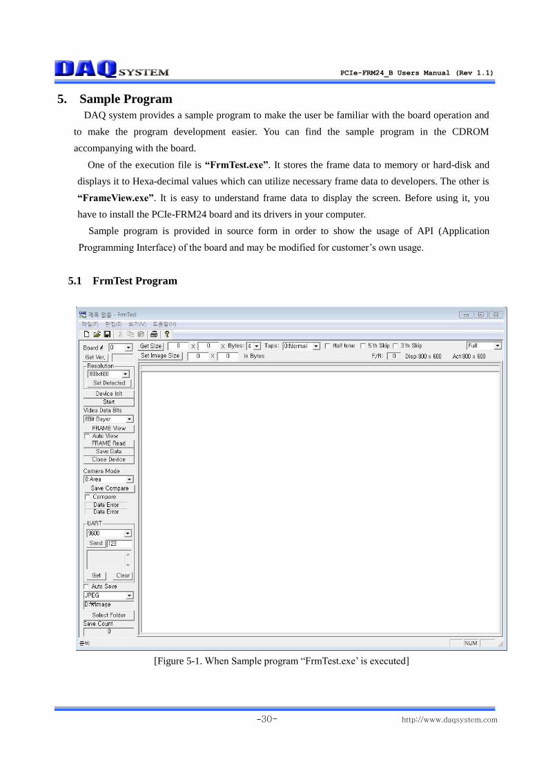
5. Sample Program
DAQ system provides a sample program to make the user be familiar with the board operation and
to make the program development easier. You can find the sample program in the CDROM
accompanying with the board.
One of the execution file is “FrmTest.exe”. It stores the frame data to memory or hard-disk and
displays it to Hexa-decimal values which can utilize necessary frame data to developers. The other is
“FrameView.exe”. It is easy to understand frame data to display the screen. Before using it, you
have to install the PCIe-FRM24 board and its drivers in your computer.
Sample program is provided in source form in order to show the usage of API (Application
Programming Interface) of the board and may be modified for customer’s own usage.
5.1 FrmTest Program
[Figure 5-1. When Sample program “FrmTest.exe’ is executed]
PCIe-FRM24_B Users Manual (Rev 1.1)
-31- http://www.daqsystem.com
To run the sample application program, you need to use API, it is a form of client DLL. To
compile the sample source to make its executable file, you have to use Import Library files and
header files. You can find them in the CDROM. To run the .exe file, the API DLL file
(pci_frm24b.dll) must be in the same directory with the .exe file or Windows system folder.
Another method is to add the directory of API DLL file to PATH environmental variable.
Each menu bar explains as below explanation. It is not use a function without mention it.
(1) Board # selection
It can select a Board #0 ~ Board #3. (Selection J4)
(2) “Get Ver.”
It shows the version of FPGA and Firmware.
(3) “Get Size”
It gets the input image resolution of sensor.
(4) “Bytes”
It selects a Video Data Width. “0”: 8bit, ”1”: 16bit, ”2”: 32bit.
(5) “Set Image Size”
It sets the input size that user want.
(6) “Taps”
It shows Taps of Camera Mode. 0: Normal Mode, 1 : Alternate Mode
(Not currently implemented.)
(7) “Half tone” toggle
It selects a halftone.
“5’th Skip” : When this button is selected, it goes beyond the 5th byte from the image data.
“3’th Skip” : When this button is selected, it goes beyond the 3th byte from the image data.
(8) “F/R”
Frame rates/sec
(9) “Full/Top Left/Top Right/Bot. Left/Bot. Right” Selection
It shows the video of 800x600 resolution where you wish selected parts.
PCIe-FRM24_B Users Manual (Rev 1.1)
-32- http://www.daqsystem.com
(10) Resolution
User can set up the resolution is 640x480, 800x600, 1024x768, 1280x720, 1280x1024,
1600x1200, 1920x1080, 1920x1200, 2048xx1536, 2560x2048, 4080x2448.
When reinstall the resolution, “Device Init” should be re-execute.
(11) Device Init
Press this button to initialize the function of receiving image frame data. It is performed only
once after power is applied to the board.
(12) Start
Press this button to begin to save image data.
(13) Video Data Bits
You can select 8Bit, 16Bit YUV, 24Bit BGR, 8Bit Bayer, 10bit bayer.
(14) FRAME View
Press this button to read the image frame data of the board to your PC. If image frame data is
not saved on the board, you must wait until the end of data collection.
Auto View” : If checked, it shows continuously.
(15) Save Data
Press this button, the image begins to save in binary form to the PC.
(16) Close Device
Press this button to finish usage of the board and terminate the program.
(17) Camera Mode
Line or Area select a camera image according to the input.
0 : Area 1 : Line (Freerun) 2: Line (Ext) 3: Line (Int)
(18) ”Save Compare”
“Compare” :Shows the number of false-bytes that compare between the saved file and
the original file.
(19) “UART” selection
Select the Baud Rate (9600, 19200, 38400, 57600, 115200 Baud Rate).

PCIe-FRM24_B Users Manual (Rev 1.1)
-33- http://www.daqsystem.com
(20) “Send” button
Send the UART data..
(21) “Get” button
Get the data from UART buffer.
(22) “Clear” button
Clear the UART Receiver buffer.
(23) Auto Save
When check this box, it save a file by BMP or JPEG format each 30 frames per 1 second until
un-check this box.
(24) Select Folder
It selects a folder for saving. It set “D:\Image” folder basically.
PCIe-FRM24_B Users Manual (Rev 1.1)
-34- http://www.daqsystem.com
Appendix
A.1 General Specification
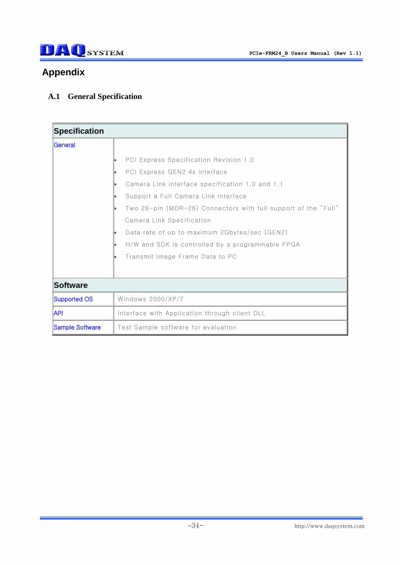
Specification
General
PCI Express Specif ication Revision 1.0
PCI Express GEN2 4x interface
Camera Link interface specification 1.0 and 1.1
Support a Full Camera Link Interface
Two 26-pin (MDR-26) Connectors with full support of the “Full”
Camera Link Specification
Data rate of up to maximum 2Gbytes/sec (GEN2)
H/W and SDK is controlled by a programmable FPGA
Transmit Image Frame Data to PC
Software
Supported OS Windows 2000/XP/7
API Interface with Application through client DLL
Sample Software Test Sample software for evaluation
PCIe-FRM24_B Users Manual (Rev 1.1)
-35- http://www.daqsystem.com
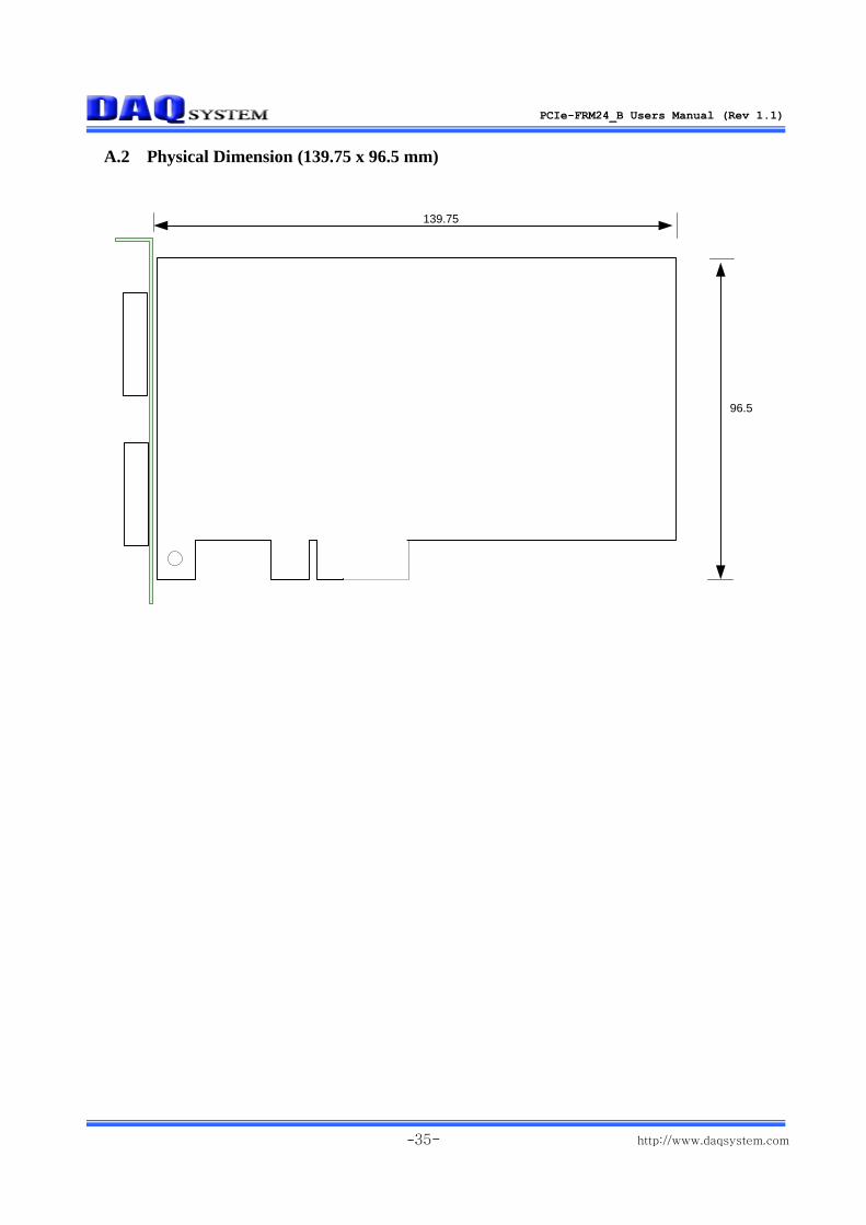
A.2 Physical Dimension (139.75 x 96.5 mm)
139.75
96.5
PCIe-FRM24_B Users Manual (Rev 1.1)
-36- http://www.daqsystem.com
References
1. How to install PCI DAQ Board
-- DAQ system
2. AN201 How to build application using API
-- DAQ system
3. AN312 PCIe-FRM24_B API Programming
-- DAQ system