Embed Size (px)
Citation preview

PHYS 319
● Things to do before next week's lab● Whirlwind tour of the MSP430 CPU and its
assembly language● Activity 1.

● Read manual for Lab 2 and your OS setup guide then prepare your computer (assembler and flasher), or plan to use the lab computers and read their guide, before coming to the lab!
● Get a PHAS ID from Henn 205 if you don't have one.
● Read up on binary and hexadecimal if you're not familiar with them.
Before next week's lab:

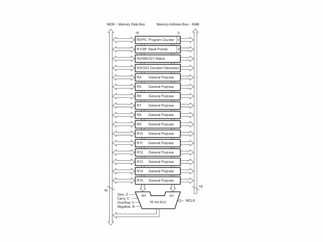
Registers:
PC – program counter
SP – stack pointer
SR – status register
CG2 – constant generator
R4-R15 -general purpose registers
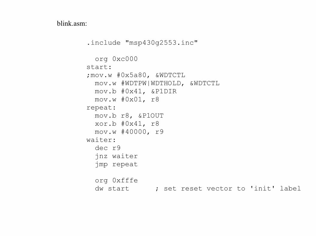
blink.asm:
.include "msp430g2553.inc"
org 0xc000start:;mov.w #0x5a80, &WDTCTL mov.w #WDTPW|WDTHOLD, &WDTCTL mov.b #0x41, &P1DIR mov.w #0x01, r8repeat: mov.b r8, &P1OUT xor.b #0x41, r8 mov.w #40000, r9waiter: dec r9 jnz waiter jmp repeat
org 0xfffe dw start ; set reset vector to 'init' label

blink.asm:
.include "msp430g2553.inc"
org 0xc000start:;mov.w #0x5a80, &WDTCTL mov.w #WDTPW|WDTHOLD, &WDTCTL mov.b #0x41, &P1DIR mov.w #0x01, r8repeat: mov.b r8, &P1OUT xor.b #0x41, r8 mov.w #40000, r9waiter: dec r9 jnz waiter jmp repeat
org 0xfffe dw start ; set reset vector to 'init' label

Assembler Commands:
• .include
• Example: .include "msp430g2553.inc"
• Instructs the assembler to include the contents of the file msp430g2553.inc into the program. This particular file contains definitions of registers and other names, but any other file, for example containing part of the program, can be included

blink.asm:
.include "msp430g2553.inc"
org 0xc000start:;mov.w #0x5a80, &WDTCTL mov.w #WDTPW|WDTHOLD, &WDTCTL mov.b #0x41, &P1DIR mov.w #0x01, r8repeat: mov.b r8, &P1OUT xor.b #0x41, r8 mov.w #40000, r9waiter: dec r9 jnz waiter jmp repeat
org 0xfffe dw start ; set reset vector to 'init' label

Assembler Commands:
• org
• Example org 0xc000
• To define the address where the next lines of the program or data are going to be stored.
• Example org 0xFFFE
• To store the address pointing to where the program should start after a reset
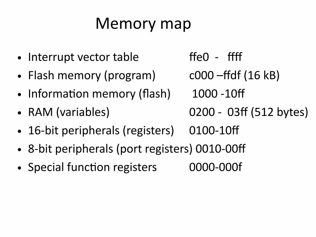
Memory map
• Interrupt vector table ffe0 - ffff
• Flash memory (program) c000 –ffdf (16 kB)
• Information memory (flash) 1000 -10ff
• RAM (variables) 0200 - 03ff (512 bytes)
• 16-bit peripherals (registers) 0100-10ff
• 8-bit peripherals (port registers) 0010-00ff
• Special function registers 0000-000f

blink.asm:
.include "msp430g2553.inc"
org 0xc000start:;mov.w #0x5a80, &WDTCTL mov.w #WDTPW|WDTHOLD, &WDTCTL mov.b #0x41, &P1DIR mov.w #0x01, r8repeat: mov.b r8, &P1OUT xor.b #0x41, r8 mov.w #40000, r9waiter: dec r9 jnz waiter jmp repeat
org 0xfffe dw start ; set reset vector to 'init' label

Assembler Commands:
;mov.w
lines beginning with ; are commentsand are ignored by the assembler

blink.asm:
.include "msp430g2553.inc"
org 0xc000start:;mov.w #0x5a80, &WDTCTL mov.w #WDTPW|WDTHOLD, &WDTCTL mov.b #0x41, &P1DIR mov.w #0x01, r8repeat: mov.b r8, &P1OUT xor.b #0x41, r8 mov.w #40000, r9waiter: dec r9 jnz waiter jmp repeat
org 0xfffe dw start ; set reset vector to 'init' label

Assembler Commands:
• dw• Define word
• Example:
dw start• Will put a 16 bit number into the next memory
location• Word start is defined as hexadecimal number
c000 (beginning of the flash memory) because it is a label immediately following the command org 0xc000

Assembler Commands:
• equ
• definition of a name for a number
• Example
P1OUT equ 0x0021• This command is used in the file
msp430g2553.inc to call hexadecimal number 0021 “P1OUT”

.include "msp430g2553.inc"
org 0xc000start:;mov.w #0x5a80, &WDTCTL mov.w #WDTPW|WDTHOLD, &WDTCTL mov.b #0x41, &P1DIR mov.w #0x01, r8repeat: mov.b r8, &P1OUT xor.b #0x41, r8 mov.w #40000, r9waiter: dec r9 jnz waiter jmp repeat
org 0xfffe dw start ; set reset vector to 'init' label
blink.asm:

Microprocessor Commands:
• Move Byte
• Example:
mov.b #0x41, &P1DIR
• P1DIR is an address of the port control register defined in the file msp430g2553.inc

Microprocessor Commands:
• bis.w
• Set a bit in a 16 bit register
• Example:
bis.w #CPUOFF,SR
• Sets a particular bit in the Status Register
• The symbol CPUOFF must be defined earlier (eg inmsp430g2553.inc)

Status Register bits
• N Negative bit. This bit is set when the result of a byte or word operation is negative and cleared when the result is not negative.
– Word operation: N is set to the value of bit 15 of the result
– Byte operation: N is set to the value of bit 7 of the result
• Z Zero bit. This bit is set when the result of a byte or word operation is 0 and cleared when the result is not 0.
• C Carry bit. This bit is set when the result of a byte or word operation produced a carry and cleared when no carry occurred.
•
V Overflow bit. Set if an operation overflows the signed variable range
••
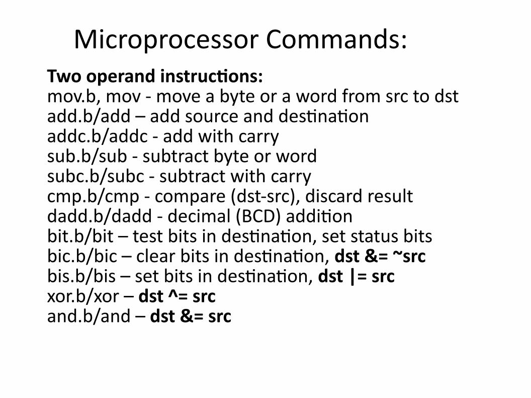
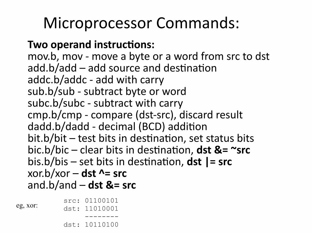
Microprocessor Commands: Two operand instructions:mov.b, mov - move a byte or a word from src to dstadd.b/add – add source and destinationaddc.b/addc - add with carrysub.b/sub - subtract byte or wordsubc.b/subc - subtract with carrycmp.b/cmp - compare (dst-src), discard resultdadd.b/dadd - decimal (BCD) additionbit.b/bit – test bits in destination, set status bitsbic.b/bic – clear bits in destination, dst &= ~srcbis.b/bis – set bits in destination, dst |= srcxor.b/xor – dst ^= srcand.b/and – dst &= src
Microprocessor Commands: Two operand instructions:mov.b, mov - move a byte or a word from src to dstadd.b/add – add source and destinationaddc.b/addc - add with carrysub.b/sub - subtract byte or wordsubc.b/subc - subtract with carrycmp.b/cmp - compare (dst-src), discard resultdadd.b/dadd - decimal (BCD) additionbit.b/bit – test bits in destination, set status bitsbic.b/bic – clear bits in destination, dst &= ~srcbis.b/bis – set bits in destination, dst |= srcxor.b/xor – dst ^= srcand.b/and – dst &= src
eg, xor: src: 01100101dst: 11010001 --------dst: 10110100

Microprocessor Commands:
Jump instructions and program flowJEQ/JZ Jump to label if zero bit is setJNE/JNZ Jump to label if zero bit is resetJC Jump to label if carry bit is setJNC Jump to label if carry bit is resetJN Jump to label if negative bit is setJGE Jump to label if (N .XOR. V) = 0JL Jump to label if (N .XOR. V) = 1JMP Jump to label

Microprocessor Commands: Single operand instructions:rrc.b/rrc – rotate right through carryswpb - swap bytesrra.b/rra – rotate right arithmeticsxt – sign extend byte to wordpush.b/push – push value onto stackcall – push PC on stack and move source to PCreti – return from interrupt – pop SR, then pop PC

Microprocessor Commands:
That's it! That is all the instructions the CPU understands.
In the manual, there are some additional instructions, referred to as 'emulated instructions' which are really just convenient abbreviations.

blink.asm:
.include "msp430g2553.inc"
org 0xc000start:;mov.w #0x5a80, &WDTCTL mov.w #WDTPW|WDTHOLD, &WDTCTL mov.b #0x41, &P1DIR mov.w #0x01, r8repeat: mov.b r8, &P1OUT xor.b #0x41, r8 mov.w #40000, r9waiter: dec r9 jnz waiter jmp repeat
org 0xfffe dw start ; set reset vector to 'init' label

Addressing Modes
As/Ad Addressing Mode Syntax Description
00/0 Register mode Rn Register direct. Register contents are operand
01/1 Indexed mode X(Rn) Indexed mode. The operand is in memory at address Rn+X.
01/1 Symbolic mode ADDR Symbolic mode. (PC + X) points to the operand. X is stored in the
next word. Indexed mode X(PC) is used.
01/1 Absolute mode &ADDR Absolute Mode. The word following the instruction contains the absolute
address. X is stored in the next word. Indexed mode X(SR) is used.
10/− Indirect register mode @Rn Register indirect. Rn is used as a pointer to the operand. (same as 0(Rn) )
11/− Indirect autoincrement @Rn+ Register autoincrment. Rn is used as a pointer to the operand. Rn is incremented
afterwards by 1 for .B instructions and by 2 for .W instructions.
11/− Immediate mode #N Immediate Mode. The word following the instruction contains the immediate
constant N. Indirect autoincrementmode @PC+ is used.

Addressing Modes
• Immediate mode
• Syntax: #N
• The word following the instruction contains the immediate constant N.
• Examples:
mov.b #01000001b, & P1DIR
• Source address can use this format (destination cannot)
mov.b #65, & P1DIR
mov.b #0x41, & P1DIR

Addressing Modes
• Absolute mode
• Syntax: & ADDR
• The word following the instruction contains the absolute address.
• Example:
mov.b #11110111b, & P1DIR
The destination address uses this format

Addressing Modes
• Register mode
• Syntax Rn
• Register contents are operand
• Rn can be PC, SP, SR, CG2, R4 ...R16
• Example
bis.w #CPUOFF,SR
Destination address is the CPU status register SR
Addressing Modes
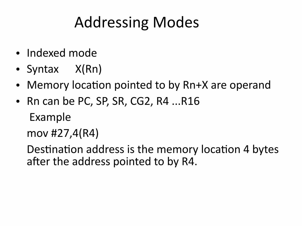
• Indexed mode
• Syntax X(Rn)
• Memory location pointed to by Rn+X are operand
• Rn can be PC, SP, SR, CG2, R4 ...R16
Example
mov #27,4(R4)
Destination address is the memory location 4 bytesafter the address pointed to by R4.

Addressing Modes
As/Ad Addressing Mode Syntax Description
00/0 Register mode Rn Register direct. Register contents are operand
01/1 Indexed mode X(Rn) Indexed mode. The operand is in memory at address Rn+X.
01/1 Symbolic mode ADDR Symbolic mode. (PC + X) points to the operand. X is stored in the
next word. Indexed mode X(PC) is used.
01/1 Absolute mode &ADDR Absolute Mode. The word following the instruction contains the absolute
address. X is stored in the next word. Indexed mode X(SR) is used.
10/− Indirect register mode @Rn Register indirect. Rn is used as a pointer to the operand. (same as 0(Rn) )
11/− Indirect autoincrement @Rn+ Register autoincrment. Rn is used as a pointer to the operand. Rn is incremented
afterwards by 1 for .B instructions and by 2 for .W instructions.
11/− Immediate mode #N Immediate Mode. The word following the instruction contains the immediate
constant N. Indirect autoincrementmode @PC+ is used.
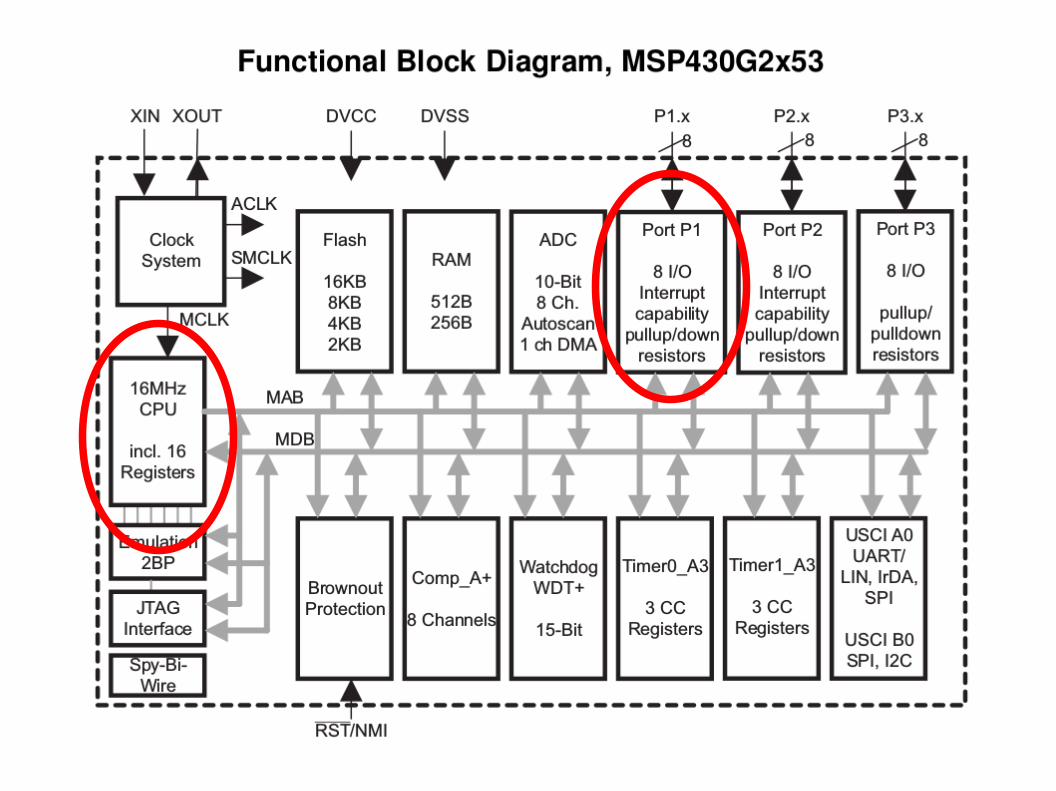
General Purpose Input/Output (GPIO) Ports
Several registers control the configuration and operation of sets of pins.In these registers, the different bits in the register control different pins.
P1DIR – sets the pin directions. Bit = 0 = input, Bit = 1 = output.
P1IN – input register. When configured for input, this register contains the digital input values
P1OUT – output register. When configured for output, writing to this register sets the outputs
P1REN – pullup/pulldown enable. Bit = 1, enable resistor (P1OUT sets whether pullup or down).
P1SEL/P1SEL2 – alternate function enable – both 0 means GPIO.
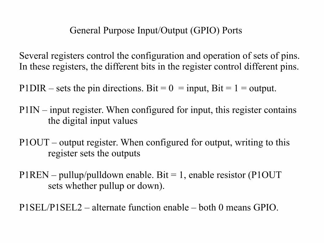
eg setting P1DIR = 3 (00000011b) configures pins P1.0 and P1.1 as outputs, P1.2-P1.7 as inputs

Activity 1• Write commands which will configure all pins of port
1 as inputs, and move the value from port 1 to register R7. Finally, write the binary number which will be in the 16 bit register R7 after these operations assuming that all 8 pins of port 1 were connected to 3V.
• Port P1 registers:
• P1REN ; Port P1 resistor enable
• P1SEL ; Port P1 selection
• P1DIR ; Port P1 direction
• P1OUT ; Port P1 output
• P1IN ; Port P1 input