Embed Size (px)
Citation preview
1
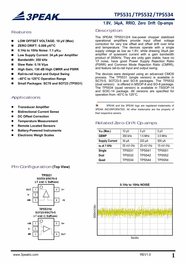
TP5531 / TP5532 / TP5534
1.8V, 34μA, RRIO, Zero Drift Op-amps
www.3peakic.com REV1.0
Features
LOW OFFSET VOLTAGE: 10 μV (Max)
ZERO DRIFT: 0.008 µV/°C
0.1Hz to 10Hz Noise: 1.1 µVPP
Low Supply Current: 34µA per Amplifier
Bandwidth: 350 kHz
Slew Rate: 0.16 V/μs
High Gain, 130 dB High CMRR and PSRR
Rail-to-rail Input and Output Swing
–40°C to 125°C Operation Range
Small Packages: SC70 and SOT23 (TP5531)
Applications
Transducer Amplifier
Bidirectional Current Sense
DC Offset Correction
Temperature Measurement
Remote Located Sensors
Battery-Powered Instruments
Electronic Weigh Scales
Pin Configuration (Top View)
Description
The 3PEAK TP5531/2/4 low-power chopper stabilized operational amplifiers provide input offset voltage correction for very low offset and offset drift over time and temperature. The devices operate with a single supply voltage as low as 1.8V, while drawing 34μA per amplifier of quiescent current with a gain bandwidth product of 350kHz. They are unity gain stable, have no 1/f noise, have good Power Supply Rejection Ratio (PSRR) and Common Mode Rejection Ratio (CMRR), and feature rail-to-rail input and output swing.
The devices were designed using an advanced CMOS process. The TP5531 (single version) is available in SC70-5, SOT23-5 and SO-8 packages. The TP5532 (dual version) is offered in MSOP-8 and SO-8 package. The TP5534 (quad version) is available in TSSOP-14 and SOIC-14 package. All versions are specified for operation from -40°C to 125°C.
3PEAK and the 3PEAK logo are registered trademarks of
3PEAK INCORPORATED. All other trademarks are the property of
their respective owners.
Related Zero-Drift Op-amps
VOS (Max.) 10 μV 5 μV 5 μV
GBWP 350 kHz 1.5 MHz 3.5 MHz
Supply Current 34 μA 220 μA 500 μA
eN at 1 kHz 55 nV/√Hz 25 nV/√Hz 15 nV/√Hz
Single TP5531 TP5541 TP5551
Dual TP5532 TP5542 TP5552
Quad TP5534 TP5544 TP5554
50
0nV
/div
5s/div
0.1Hz to 10Hz NOISE
2 REV1.0 www.3peakic.com
TP5531 / TP5532/TP5534
1.8V, 34μA, RRIO, Zero Drift Op-amps
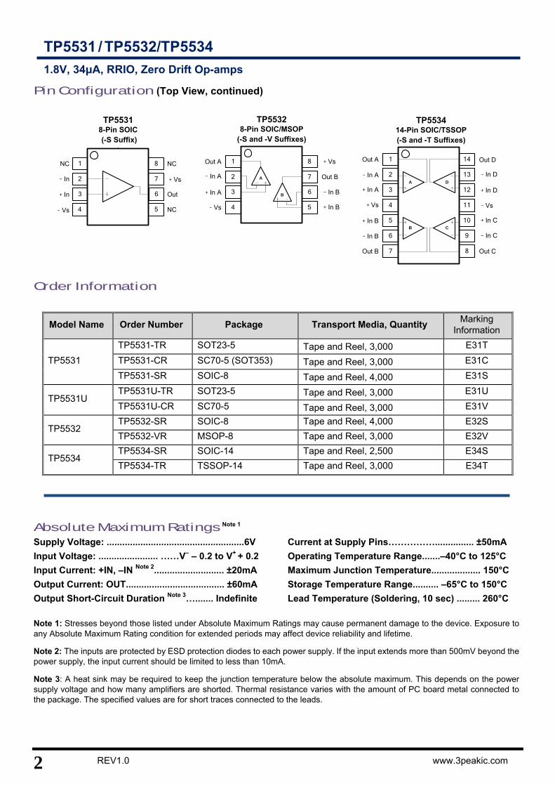
Pin Configuration (Top View, continued)
8
6
5
7
3
2
1
4
NC
﹣Vs
﹢In
﹣In ﹢Vs
Out
NC
NC
TP55318-Pin SOIC(-S Suffix)
TP553414-Pin SOIC/TSSOP(-S and -T Suffixes)
14
13
12
11
10
9
8
6
5
7
3
2
1
4
Out A
﹢In A
﹣In ADA
CB
Out D
﹢In D
﹣In D
Out B
﹢In B
﹣In B
Out C
﹢In C
﹣In C
﹣Vs﹢Vs
TP55328-Pin SOIC/MSOP
(-S and -V Suffixes)
8
6
5
7
3
2
1
4
Out A
﹢In A
﹣In A
﹢In B
﹣In B
Out BA
B
﹣Vs
﹢Vs
Order Information
Model Name Order Number Package Transport Media, Quantity Marking
Information
TP5531
TP5531-TR SOT23-5 Tape and Reel, 3,000 E31T
TP5531-CR SC70-5 (SOT353) Tape and Reel, 3,000 E31C
TP5531-SR SOIC-8 Tape and Reel, 4,000 E31S
TP5531U TP5531U-TR SOT23-5 Tape and Reel, 3,000 E31U
TP5531U-CR SC70-5 Tape and Reel, 3,000 E31V
TP5532 TP5532-SR SOIC-8 Tape and Reel, 4,000 E32S
TP5532-VR MSOP-8 Tape and Reel, 3,000 E32V
TP5534 TP5534-SR SOIC-14 Tape and Reel, 2,500 E34S
TP5534-TR TSSOP-14 Tape and Reel, 3,000 E34T
Absolute Maximum Ratings Note 1
Supply Voltage: .....................................................6V
Input Voltage: ....................... ……V– – 0.2 to V+ + 0.2
Input Current: +IN, –IN Note 2........................... ±20mA
Output Current: OUT...................................... ±60mA
Output Short-Circuit Duration Note 3…....... Indefinite
Current at Supply Pins……………............... ±50mA
Operating Temperature Range.......–40°C to 125°C
Maximum Junction Temperature................... 150°C
Storage Temperature Range.......... –65°C to 150°C
Lead Temperature (Soldering, 10 sec) ......... 260°C
Note 1: Stresses beyond those listed under Absolute Maximum Ratings may cause permanent damage to the device. Exposure to any Absolute Maximum Rating condition for extended periods may affect device reliability and lifetime.
Note 2: The inputs are protected by ESD protection diodes to each power supply. If the input extends more than 500mV beyond the power supply, the input current should be limited to less than 10mA.
Note 3: A heat sink may be required to keep the junction temperature below the absolute maximum. This depends on the power supply voltage and how many amplifiers are shorted. Thermal resistance varies with the amount of PC board metal connected to the package. The specified values are for short traces connected to the leads.
3
TP5531 / TP5532/TP5534
1.8V, 34μA, RRIO, Zero Drift Op-amps
www.3peakic.com REV1.0
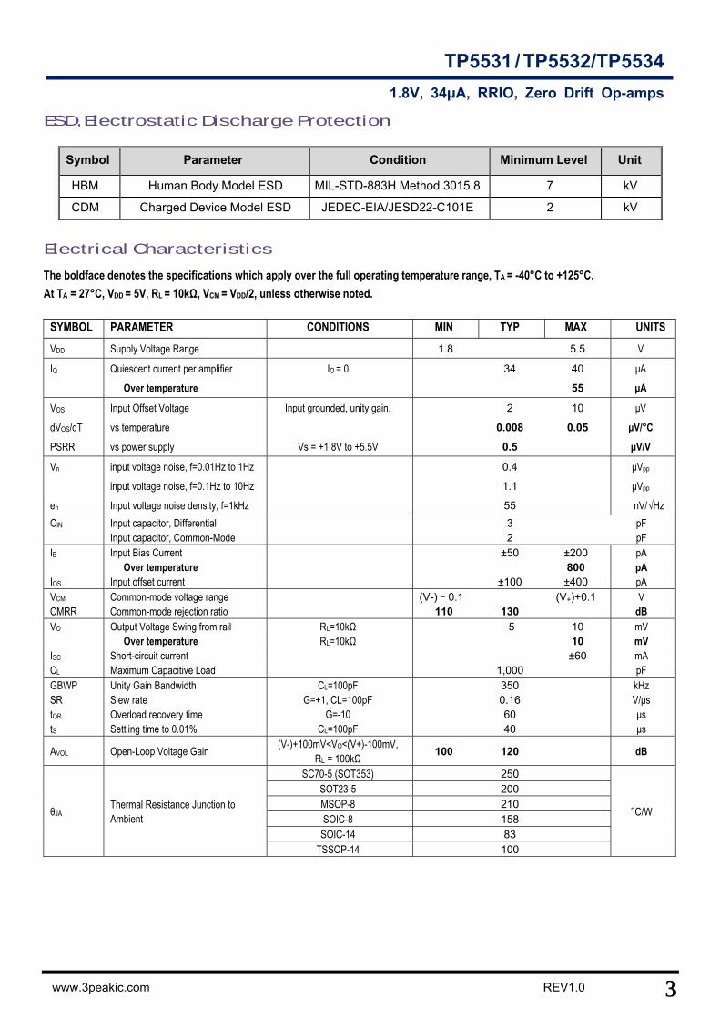
ESD, Electrostatic Discharge Protection
Symbol Parameter Condition Minimum Level Unit
HBM Human Body Model ESD MIL-STD-883H Method 3015.8 7 kV
CDM Charged Device Model ESD JEDEC-EIA/JESD22-C101E 2 kV
Electrical Characteristics
The boldface denotes the specifications which apply over the full operating temperature range, TA = -40°C to +125°C.
At TA = 27°C, VDD = 5V, RL = 10kΩ, VCM = VDD/2, unless otherwise noted.
SYMBOL PARAMETER CONDITIONS MIN TYP MAX UNITS
VDD Supply Voltage Range 1.8 5.5 V
IQ Quiescent current per amplifier IO = 0 34 40 μA
Over temperature 55 μA
VOS Input Offset Voltage Input grounded, unity gain. 2 10 μV
dVOS/dT vs temperature 0.008 0.05 μV/°C
PSRR vs power supply Vs = +1.8V to +5.5V 0.5 μV/V
Vn input voltage noise, f=0.01Hz to 1Hz 0.4 μVpp
input voltage noise, f=0.1Hz to 10Hz 1.1 μVpp
en Input voltage noise density, f=1kHz 55 nV/√Hz
CIN Input capacitor, Differential 3 pF Input capacitor, Common-Mode 2 pF IB Input Bias Current ±50 ±200 pA Over temperature 800 pA IOS Input offset current ±100 ±400 pA VCM Common-mode voltage range (V-)–0.1 (V+)+0.1 V CMRR Common-mode rejection ratio 110 130 dB VO Output Voltage Swing from rail RL=10kΩ 5 10 mV Over temperature RL=10kΩ 10 mV ISC Short-circuit current ±60 mA CL Maximum Capacitive Load 1,000 pF GBWP Unity Gain Bandwidth CL=100pF 350 kHz SR Slew rate G=+1, CL=100pF 0.16 V/μs tOR Overload recovery time G=-10 60 μs tS Settling time to 0.01% CL=100pF 40 μs
AVOL Open-Loop Voltage Gain (V-)+100mV<VO<(V+)-100mV,
RL = 100kΩ 100 120 dB
θJA Thermal Resistance Junction to Ambient
SC70-5 (SOT353) 250
°C/W
SOT23-5 200 MSOP-8 210 SOIC-8 158 SOIC-14 83
TSSOP-14 100
4 REV1.0 www.3peakic.com
TP5531 / TP5532/TP5534
1.8V, 34μA, RRIO, Zero Drift Op-amps
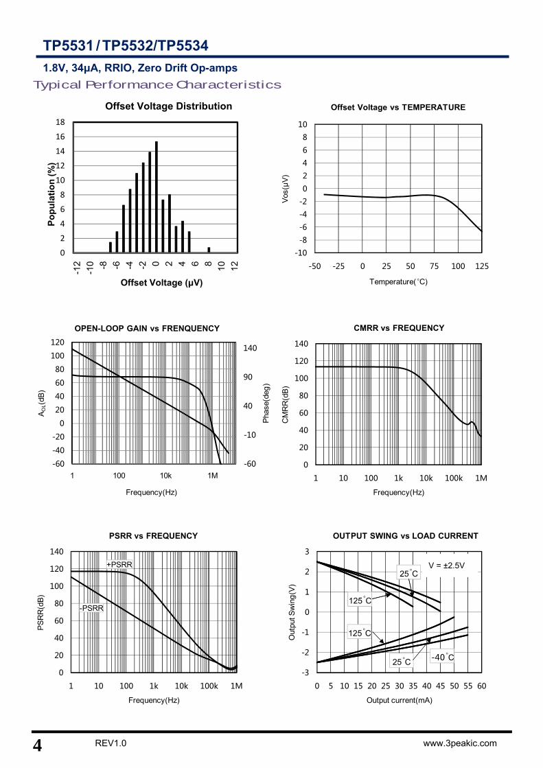
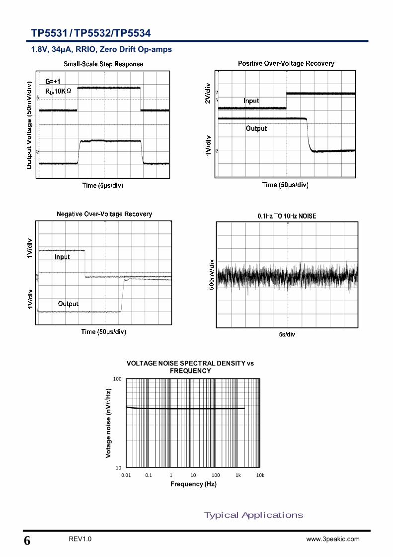
Typical Performance Characteristics
0
2
4
6
8
10
12
14
16
18
-12
-10 -8 -6 -4 -2 0 2 4 6 8 10 12
Po
pu
lati
on
(%
)
Offset Voltage (μV)
Offset Voltage Distribution
-60
-10
40
90
140
-60
-40
-20
0
20
40
60
80
100
120
1 100 10k 1M
AO
L(dB
)
Frequency(Hz)
OPEN-LOOP GAIN vs FRENQUENCY
Pha
se(d
eg)
0
20
40
60
80
100
120
140
1 10 100 1k 10k 100k 1M
CM
RR
(dB
)
Frequency(Hz)
CMRR vs FREQUENCY
0
20
40
60
80
100
120
140
1 10 100 1k 10k 100k 1M
PS
RR
(dB
)
Frequency(Hz)
PSRR vs FREQUENCY
-PSRR
+PSRR
-3
-2
-1
0
1
2
3
0 5 10 15 20 25 30 35 40 45 50 55 60
Out
put S
win
g(V
)
Output current(mA)
OUTPUT SWING vs LOAD CURRENT
25°C
125°C
25。C
125。C
125。C
25。C -40
。C
-10
-8
-6
-4
-2
0
2
4
6
8
10
-50 -25 0 25 50 75 100 125
Vos
(μV
)Temperature(°C)
Offset Voltage vs TEMPERATURE
V = ±2.5V
5
TP5531 / TP5532/TP5534
1.8V, 34μA, RRIO, Zero Drift Op-amps
www.3peakic.com REV1.0
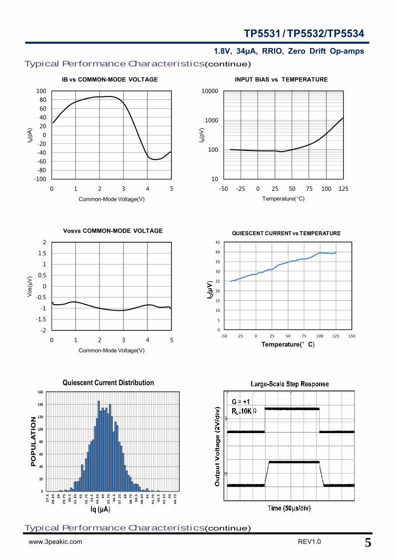
Typical Performance Characteristics(continue)
Typical Performance Characteristics(continue)
-100-80-60-40-20
020406080
100
0 1 2 3 4 5
I B(p
A)
Common-Mode Voltage(V)
IB vs COMMON-MODE VOLTAGE
10
100
1000
10000
-50 -25 0 25 50 75 100 125
I B(p
V)
Temperature(°C)
INPUT BIAS vs TEMPERATURE
-2
-1.5
-1
-0.5
0
0.5
1
1.5
2
0 1 2 3 4 5
Vos
(μV
)
Common-Mode Voltage(V)
Vosvs COMMON-MODE VOLTAGE
0
5
10
15
20
25
30
35
40
45
‐50 ‐25 0 25 50 75 100 125 150
I Q(μ
V)
Temperature(°C)
QUIESCENT CURRENT vs TEMPERATURE
0
20
40
60
80
100
120
140
160
27.5
28.25
29
29.75
30.5
31.25
32
32.75
33.5
34.25
35
35.75
36.5
37.25
38
38.75
39.5
40.25
41
41.75
42.5
43.25
44
44.75
PO
PU
LA
TIO
N
Iq (μA)
Quiescent Current Distribution
6 REV1.0 www.3peakic.com
TP5531 / TP5532/TP5534
1.8V, 34μA, RRIO, Zero Drift Op-amps
Typical Applications
10
100
0.01 0.1 1 10 100 1k 10k
Vo
tag
e n
ois
e (
nV
/√H
z)
Frequency (Hz)
VOLTAGE NOISE SPECTRAL DENSITY vs FREQUENCY
7
TP5531 / TP5532/TP5534
1.8V, 34μA, RRIO, Zero Drift Op-amps
www.3peakic.com REV1.0
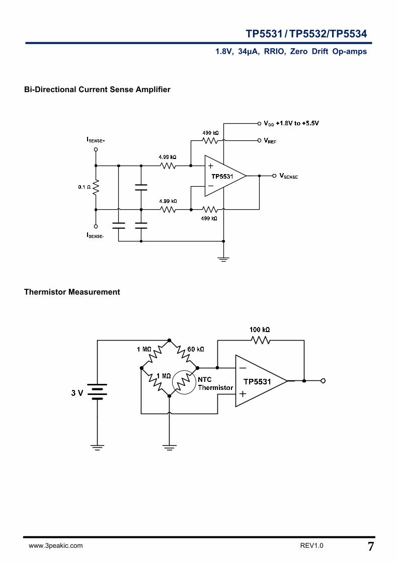
Bi-Directional Current Sense Amplifier
Thermistor Measurement
8 REV1.0 www.3peakic.com
TP5531 / TP5532/TP5534
1.8V, 34μA, RRIO, Zero Drift Op-amps
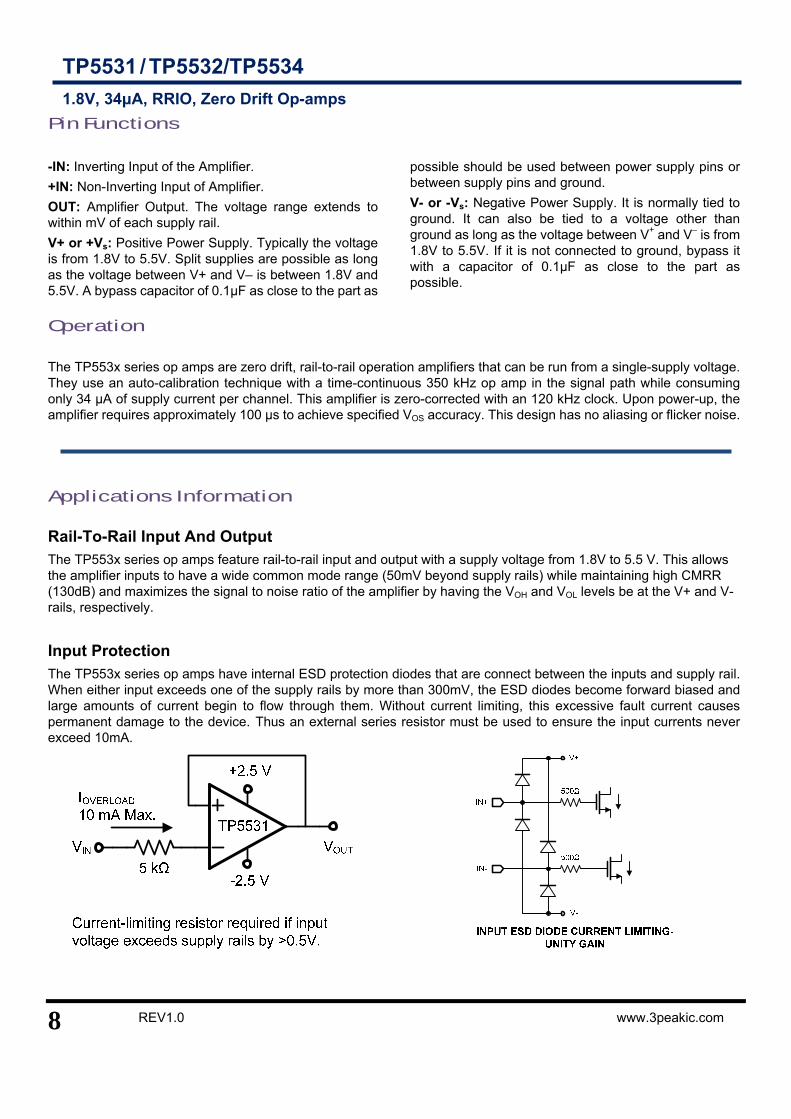
Pin Functions -IN: Inverting Input of the Amplifier.
+IN: Non-Inverting Input of Amplifier.
OUT: Amplifier Output. The voltage range extends to within mV of each supply rail.
V+ or +Vs: Positive Power Supply. Typically the voltage is from 1.8V to 5.5V. Split supplies are possible as long as the voltage between V+ and V– is between 1.8V and 5.5V. A bypass capacitor of 0.1μF as close to the part as
possible should be used between power supply pins or between supply pins and ground.
V- or -Vs: Negative Power Supply. It is normally tied to ground. It can also be tied to a voltage other than ground as long as the voltage between V+ and V– is from 1.8V to 5.5V. If it is not connected to ground, bypass it with a capacitor of 0.1μF as close to the part as possible.
Operation
The TP553x series op amps are zero drift, rail-to-rail operation amplifiers that can be run from a single-supply voltage. They use an auto-calibration technique with a time-continuous 350 kHz op amp in the signal path while consuming only 34 μA of supply current per channel. This amplifier is zero-corrected with an 120 kHz clock. Upon power-up, the amplifier requires approximately 100 μs to achieve specified VOS accuracy. This design has no aliasing or flicker noise.
Applications Information Rail-To-Rail Input And Output The TP553x series op amps feature rail-to-rail input and output with a supply voltage from 1.8V to 5.5 V. This allows the amplifier inputs to have a wide common mode range (50mV beyond supply rails) while maintaining high CMRR (130dB) and maximizes the signal to noise ratio of the amplifier by having the VOH and VOL levels be at the V+ and V- rails, respectively.
Input Protection
The TP553x series op amps have internal ESD protection diodes that are connect between the inputs and supply rail. When either input exceeds one of the supply rails by more than 300mV, the ESD diodes become forward biased and large amounts of current begin to flow through them. Without current limiting, this excessive fault current causes permanent damage to the device. Thus an external series resistor must be used to ensure the input currents never exceed 10mA.
9
TP5531 / TP5532/TP5534
1.8V, 34μA, RRIO, Zero Drift Op-amps
www.3peakic.com REV1.0
Low Input Referred Noise
Flicker noise, as known as 1/f noise, is inherent in semiconductor devices and increases as frequency decreases. So at lower frequencies, flicker noise dominates, causing higher degrees of error for sub-Hertz frequencies or dc precision application.
The TP553x series amplifiers are chopper stabilized amplifiers, the flicker noise is reduced greatly because of this technique. This reduction in 1/f noise allows the TP553x to have much lower noise at dc and low frequency compared to standard low noise amplifier.
Residual Voltage Ripple The chopping technique can be used in amplifier design due to the internal notch filter. Although the chopping related voltage ripple is suppressed, higher noise spectrum exists at the chopping frequency and its harmonics due to residual ripple.
So if the frequency of input signal is nearby the chopping frequency, the signal maybe interfered by the residue ripple. To further suppress the noise at the chopping frequency, it is recommended that a post filter be placed at the output of the amplifier.
Broad Band and External Resistor Noise Considerations The total broadband noise output from any amplifier is primarily a function of three types of noise: input voltage noise from the amplifier, input current noise from the amplifier, and thermal (Johnson) noise from the external resistors used around the amplifier. These noise sources are not correlated with each other and their combined noise can be summed in a root sum squared manner. The full equation is given as:
2 2 1/2[ 4 ( ) ] n n s n se total e kTR i R
Where:
en= the input voltage noise density of the amplifier.
in= the input current noise of the amplifier.
RS= source resistance connected to the noninverting terminal.
k= Boltzmann’s constant (1.38x10⁻²³J/K). T= ambient temperature in Kelvin (K).
The total equivalent rms noise over a specific bandwidth is expressed as:
, n rms ne e total BW
The input voltage noise density (en) of the TP553x is 55 nV/√Hz, and the input current noise can be neglected. When the source resistance is 190 kΩ, the voltage noise contribution from the source resistor and the amplifier are equal. With source resistance greater than 190 kΩ, the overall noise of the system is dominated by the Johnson noise of the resistor itself.
High Source Impedance Application The TP553x series op amps use switches at the chopper amplifier input, the input signal is chopped at 125 kHz to reduce input offset voltage down to 10µV. The dynamic behavior of these switches induces a charge injection current to the input terminals of the amplifier. The charge injection current has a DC path to ground through the resistances seen at the input terminals of the amplifier. Higher input impedance causes an apparent shift in the input bias current of the amplifier.
Because the chopper amplifier has charge injection currents at each terminal, the input offset current will be larger than standard amplifiers. The IOS of TP553x are 150pA under the typical condition. So the input impedance should be
10 REV1.0 www.3peakic.com
TP5531 / TP5532/TP5534
1.8V, 34μA, RRIO, Zero Drift Op-amps
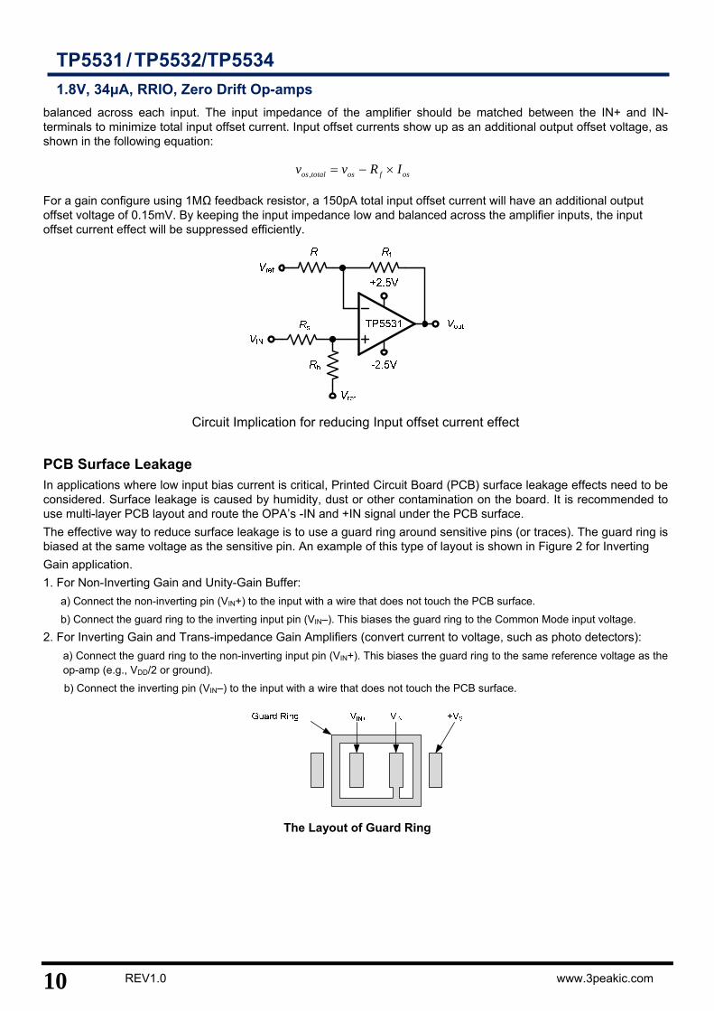
balanced across each input. The input impedance of the amplifier should be matched between the IN+ and IN- terminals to minimize total input offset current. Input offset currents show up as an additional output offset voltage, as shown in the following equation:
, os total os f osv v R I
For a gain configure using 1MΩ feedback resistor, a 150pA total input offset current will have an additional output offset voltage of 0.15mV. By keeping the input impedance low and balanced across the amplifier inputs, the input offset current effect will be suppressed efficiently.
Circuit Implication for reducing Input offset current effect
PCB Surface Leakage In applications where low input bias current is critical, Printed Circuit Board (PCB) surface leakage effects need to be considered. Surface leakage is caused by humidity, dust or other contamination on the board. It is recommended to use multi-layer PCB layout and route the OPA’s -IN and +IN signal under the PCB surface.
The effective way to reduce surface leakage is to use a guard ring around sensitive pins (or traces). The guard ring is biased at the same voltage as the sensitive pin. An example of this type of layout is shown in Figure 2 for Inverting
Gain application.
1. For Non-Inverting Gain and Unity-Gain Buffer:
a) Connect the non-inverting pin (VIN+) to the input with a wire that does not touch the PCB surface.
b) Connect the guard ring to the inverting input pin (VIN–). This biases the guard ring to the Common Mode input voltage.
2. For Inverting Gain and Trans-impedance Gain Amplifiers (convert current to voltage, such as photo detectors):
a) Connect the guard ring to the non-inverting input pin (VIN+). This biases the guard ring to the same reference voltage as the op-amp (e.g., VDD/2 or ground).
b) Connect the inverting pin (VIN–) to the input with a wire that does not touch the PCB surface.
The Layout of Guard Ring
11
TP5531 / TP5532/TP5534
1.8V, 34μA, RRIO, Zero Drift Op-amps
www.3peakic.com REV1.0
Package Outline Dimensions
SOT23-5 / SOT23-6
Symbol
Dimensions
In Millimeters
Dimensions
In Inches
Min Max Min Max
A1 0.000 0.100 0.000 0.004
A2 1.050 1.150 0.041 0.045
b 0.300 0.400 0.012 0.016
D 2.820 3.020 0.111 0.119
E 1.500 1.700 0.059 0.067
E1 2.650 2.950 0.104 0.116
e 0.950TYP 0.037TYP
e1 1.800 2.000 0.071 0.079
L1 0.300 0.460 0.012 0.024
θ 0° 8° 0° 8°
12 REV1.0 www.3peakic.com
TP5531 / TP5532/TP5534
1.8V, 34μA, RRIO, Zero Drift Op-amps
Package Outline Dimensions
SC-70-5 (SOT353)
Symbol
Dimensions
In Millimeters
Dimensions In
Inches
Min Max Min Max
A1 0.000 0.100 0.000 0.004
A2 0.900 1.000 0.035 0.039
b 0.150 0.350 0.006 0.014
C 0.080 0.150 0.003 0.006
D 2.000 2.200 0.079 0.087
E 1.150 1.350 0.045 0.053
E1 2.150 2.450 0.085 0.096
e 0.650TYP 0.026TYP
e1 1.200 1.400 0.047 0.055
L1 0.260 0.460 0.010 0.018
θ 0° 8° 0° 8°
13
TP5531 / TP5532/TP5534
1.8V, 34μA, RRIO, Zero Drift Op-amps
www.3peakic.com REV1.0
D
E1
b
E
A1
A2
e
θ
L1
C
Package Outline Dimensions
SOP-8 (SOIC-8)
Symbol
Dimensions
In Millimeters
Dimensions In
Inches
Min Max Min Max
A1 0.100 0.250 0.004 0.010
A2 1.350 1.550 0.053 0.061
b 0.330 0.510 0.013 0.020
C 0.190 0.250 0.007 0.010
D 4.780 5.000 0.188 0.197
E 3.800 4.000 0.150 0.157
E1 5.800 6.300 0.228 0.248
e 1.270 TYP 0.050 TYP
L1 0.400 1.270 0.016 0.050
θ 0° 8° 0° 8°
14 REV1.0 www.3peakic.com
TP5531 / TP5532/TP5534
1.8V, 34μA, RRIO, Zero Drift Op-amps
Package Outline Dimensions
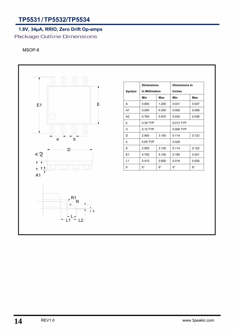
MSOP-8
Symbol
Dimensions
In Millimeters
Dimensions In
Inches
Min Max Min Max
A 0.800 1.200 0.031 0.047
A1 0.000 0.200 0.000 0.008
A2 0.760 0.970 0.030 0.038
b 0.30 TYP 0.012 TYP
C 0.15 TYP 0.006 TYP
D 2.900 3.100 0.114 0.122
e 0.65 TYP 0.026
E 2.900 3.100 0.114 0.122
E1 4.700 5.100 0.185 0.201
L1 0.410 0.650 0.016 0.026
θ 0° 6° 0° 6°
E1
e
E
A1
D
L1 L2L
RR1
θ
b
15
TP5531 / TP5532/TP5534
1.8V, 34μA, RRIO, Zero Drift Op-amps
www.3peakic.com REV1.0
Package Outline Dimensions
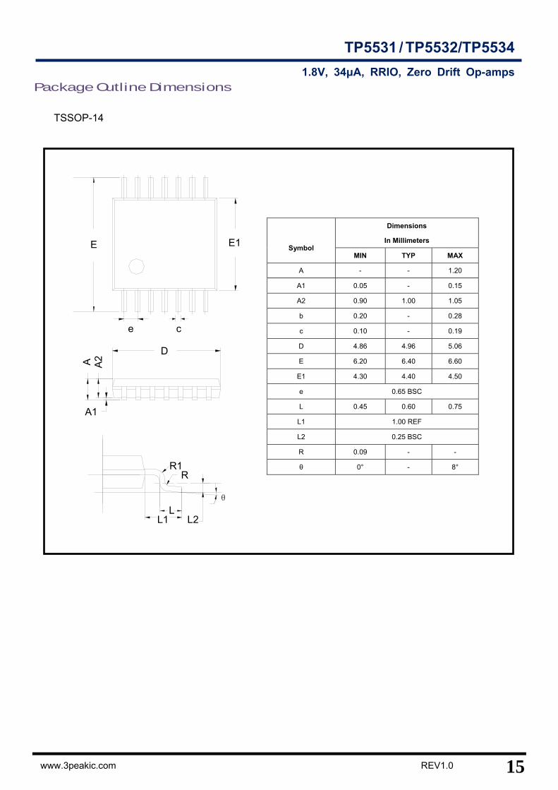
TSSOP-14
Symbol
Dimensions
In Millimeters
MIN TYP MAX
A - - 1.20
A1 0.05 - 0.15
A2 0.90 1.00 1.05
b 0.20 - 0.28
c 0.10 - 0.19
D 4.86 4.96 5.06
E 6.20 6.40 6.60
E1 4.30 4.40 4.50
e 0.65 BSC
L 0.45 0.60 0.75
L1 1.00 REF
L2 0.25 BSC
R 0.09 - -
θ 0° - 8°
E
e
E1
A1
A2A
D
L1 L2L
RR1
θ
c
16 REV1.0 www.3peakic.com
TP5531 / TP5532/TP5534
1.8V, 34μA, RRIO, Zero Drift Op-amps
Package Outline Dimensions
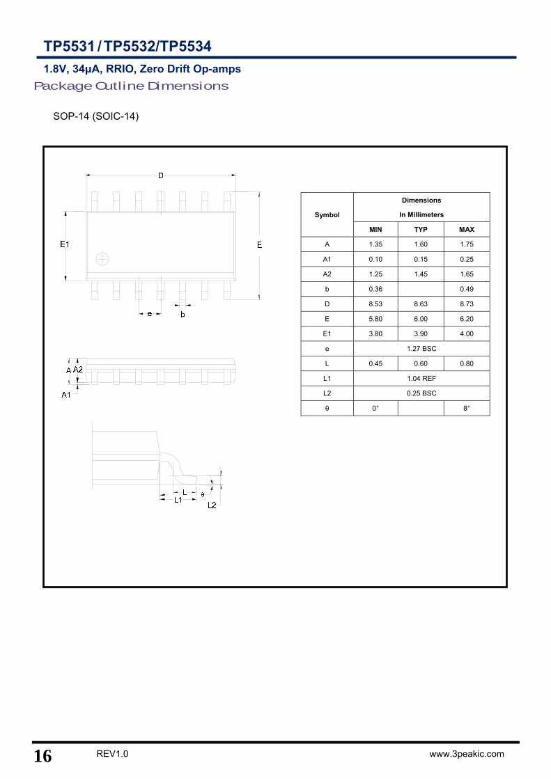
SOP-14 (SOIC-14)
Symbol
Dimensions
In Millimeters
MIN TYP MAX
A 1.35 1.60 1.75
A1 0.10 0.15 0.25
A2 1.25 1.45 1.65
b 0.36 0.49
D 8.53 8.63 8.73
E 5.80 6.00 6.20
E1 3.80 3.90 4.00
e 1.27 BSC
L 0.45 0.60 0.80
L1 1.04 REF
L2 0.25 BSC
θ 0° 8°