Embed Size (px)
Citation preview

PRINTED CIRCUIT BOARDS
PROCESS CAPABILITIES
AND
DESIGN FOR MANUFACTURE GUIDELINES
VERSION 2.7
RELEASED 04/05/2016

TABLE OF CONTENTS
Introduction ............................................................................................................................................................ 1
The Lintek Difference .............................................................................................................................................. 2
PCB Types ................................................................................................................................................................ 6
Board Layout ........................................................................................................................................................... 7
Routed Tab ......................................................................................................................................................... 7
Drilled Tab (Standard) ......................................................................................................................................... 7
Drilled Tab (Blind Snapoff) .................................................................................................................................. 7
Pinned Route ...................................................................................................................................................... 7
Process Tolerances .................................................................................................................................................. 8
Etching ................................................................................................................................................................ 8
Copper Thickness ................................................................................................................................................ 8
Drilling ................................................................................................................................................................. 9
Routing ............................................................................................................................................................. 10
Milling ............................................................................................................................................................... 10
Laser Drilling/machining ................................................................................................................................... 11
Copper Plating Blind Vias .................................................................................................................................. 11
Design for Manufacture Guidelines ...................................................................................................................... 12
Multilayer Board Layup Guide .......................................................................................................................... 12
External Layers .................................................................................................................................................. 14
Rivet Plating (copper wrap) .............................................................................................................................. 15
Internal Power and Ground Planes ................................................................................................................... 16
Pth Aspect Ratio ............................................................................................................................................... 17
Solder Mask ...................................................................................................................................................... 18
Legend .............................................................................................................................................................. 19
Surface Finishes ................................................................................................................................................ 20
Quality Assurance ............................................................................................................................................. 21
Manufacturing Lead Times ............................................................................................................................... 21
Lintek Mini Prototype Service ........................................................................................................................... 22
Job Information ..................................................................................................................................................... 23

Drawings ........................................................................................................................................................... 23
Design Files ....................................................................................................................................................... 23
Appendix 1 – Process Comparison ........................................................................................................................ 25

Process Capabilities and Design For Manufacture Guidelines Page 1 of 25
INTRODUCTION
Lintek Pty Ltd is an Australian company that has specialised in producing microwave and high frequency printed
circuit boards for 30 years. Our unique vacuum deposition metallisation process reliably produces clean,
consistent copper traces with unparalleled accuracy and excellent impedance characteristics. Our innovative,
simplistic, low cost and low risk process, produces world class products for a wide range of commercial and
defence applications.
This document serves a dual purpose. The first section outlines Lintek's manufacturing and process capabilities,
including standard board types and typical manufacturing tolerances. While we specialise in producing boards
for microwave and high frequency applications, we have a wide range of production capabilities that suits any
industry. In many cases, we are also able to tighten our process tolerances if you have specific requirements.
The remainder of the document provides Design For Manufacture “DFM” guidelines, suggesting some best
practice design rules for simple manufacture of PCBs. Designing your board in accordance with these guidelines
will ensure a smooth transition to production at Lintek.
Contact [email protected] for any sales enquiries or for further information on Lintek's process capabilities.

Process Capabilities and Design For Manufacture Guidelines Page 2 of 25
THE LINTEK DIFFERENCE
Lintek has established a strong presence in the microwave and high frequency market by producing boards
with highly accurate features and excellent impedance characteristics. Our customers like the fact that they
don’t have to tune our boards – we deliver copper features that match their designs.
Lintek can offer such excellent features due to our unique manufacturing process, vacuum metallisation. By
vacuum depositing a 2µm seed layer on bare panels instead of starting with 18µm foil, the final panel etch is
reduced to a 2µm microetch. This eliminates undercut and produces straight, accurate side walls.
Our method requires fewer process steps, uses less energy and chemicals than traditional manufacturing
methods, making Lintek’s process significantly more environmentally friendly.
Our manufacturing process starts like other manufacturers. We drill holes in a copper clad laminate, usually
starting with 18µm of copper on the panel.
Drilling
Drilledhole
18µm copper clad laminate
Lintek Other manufacturers

Process Capabilities and Design For Manufacture Guidelines Page 3 of 25
At this point, most manufacturers apply an electroless copper seed layer to enable hole plating. This is the first
of several layers of copper that they will add before stripping back a large portion at the end of the process.
Electroless copper plating requires surface preparation and often involves aggressive chemicals.
Lintek, by contrast, strips away all copper on the panel and applies a 2µm seed layer using our unique vacuum
deposition process. Since fewer chemical processes are required, this is much more environmentally friendly
and leads to a reduction in waste and chemical by-products.
Etched laminate
Metallising
Copper panel plating
Plating resist film
2µm metallised copper 0.4µm electroless copper
5µm copper panel plating
Bulk etching
Lintek Other manufacturers
Conditioner
Microetch
Initiator
Electroless Copper

Process Capabilities and Design For Manufacture Guidelines Page 4 of 25
With this seed layer applied, we can then pattern plate the features on the panel with a standard copper
electroplating process. After applying a photoimageable plate resist layer, Lintek only requires one process that
electroplates 45µm of copper onto our seed layer. Other manufacturers also need to electroplate a tin etch
resist layer in preparation for final etchback.
Electroplated tin
Electroplated copper
50µm resist film 38µm resist film
25µm electrodeposited copper45µm electrodeposited copper
3µm electrodeposited tin (etch resist)
Plating resist film
Lintek Other manufacturers
Photoresist strip

Process Capabilities and Design For Manufacture Guidelines Page 5 of 25
When the photoresist is removed, the exposed copper can be etched back to expose the substrate. Lintek only
performs a small microetch at this point, removing the 2µm of copper to strip away the seed layer. Stripping
such a small amount of copper means that no etch resist is required.
By contrast, other manufacturers perform a heavy etch. The removal of 25µm of copper requires a much
longer exposure to the etchant and results in sidewall etching. An additional process is also required to strip
the layer of tin from the finished board.
25µm heavy etch
Tin strip
2-3µm microetch
Photoresist strip
No undercut
Undercut in copper
Varying copper thickness results in weak points
Final Etch
Lintek Other manufacturers
In the standard process, the variation in copper thickness between the barrel plating and the surface can
produce weakness in the corners of plated through holes. Since Lintek’s process maintains uniform plating on
all surfaces of the panel, the plated through holes are more reliable under a range of conditions.
Lintek’s vapor deposition process eliminates many chemical compounds and process steps used in the
manufacture of printed circuit boards, including palladium chloride, formaldehyde, complexed coppers,
reducing agents, stannous chloride, sodium etch, tin plating and tin stripping.
Our simpler process reduces chemical usage, costs and outputs a superior product. A full comparison between
our method and a standard manufacturing process is shown in Appendix 1 – Process Comparison.

Process Capabilities and Design For Manufacture Guidelines Page 6 of 25
PCB TYPES
We are able to produce boards of the following types:
• single sided
• double sided
• edge plated
• multilayers with up to 12 layers, including mixed dielectrics
• HDI multilayers with laser drilled micro vias
• metal backed PTFE including blind vias
Lintek has experience working with a wide range of materials. Available substrates include:
• polyimide
• FR4
• ceramic thermoset
• PTFE and ceramic loaded PTFE
• CNC machined metal backed carriers
Lintek maintains a stock of standard and specialist materials. We are also able to work with customer supplied
laminates.
PANEL SIZES
Board Type Maximum Panel Size Maximum Usable Area Maximum
Thickness (mm) in mm in mm
Single Sided 18×24 457×610 17×23 432×584 3.2*
Single Sided (Long)# 24×72 610×1829 23×71 584×1803 3.2*
Double Sided 18×24 457×610 17×23 432×584 3.2*
Double Sided (Long)# 24×72 610×1829 23×71 584×1803 3.2*
Double Sided with Plated Through Holes
18×24 457×610 17×23 432×584 3.2*
Multilayer 18×24 457×610 17×23 432×584 6
Metal Backed 16×12 406×305 15×11 381×280 6
* Custom built multilayers using thicker laminates are available on request.
# Long boards can be produced up to 1800mm in length, without plated through holes, solder mask or
legend.

Process Capabilities and Design For Manufacture Guidelines Page 7 of 25
BOARD LAYOUT
When positioning boards on the usable area of a panel, we offer the following options:
ROUTED TAB
Route along the outline of the board, leaving tabs to hold the boards on the panel until manually separated.
DRILLED TAB (STANDARD)
Similar to Routed Tabs but with a series of holes drilled in the tab. Provides a cleaner break with less clean-up required.
DRILLED TAB (BLIND SNAPOFF)
A variety of drilled tab that ensures external dimensional tolerances are maintained without further finishing. Requires additional clearances between drilled holes and copper features.
PINNED ROUTE
Pins hold the boards in position while the outline is routed. Provides the cleanest finish, but requires 2 positioning pins on every board.

Process Capabilities and Design For Manufacture Guidelines Page 8 of 25
PROCESS TOLERANCES
ETCHING
Due to Lintek's unique metallising process, we are able to produce conductors with an etch factor of zero. By
starting with a thin copper seed layer, the amount of copper removed in the final etch is reduced significantly.
This method decreases undercut and produces cleaner features with straight sidewalls.
Typical profile of etched conductor
Straight walls produced by Lintek process
The standard tolerance on the width of all electroplated tracks and spaces is ±0.012mm.
The special tolerance on the width of all electroplated tracks and spaces is ±0.008mm.*
Track Width ± 8µm
Space Width ± 8µm
*The etch tolerance can vary slightly with different materials and surface finish requirements. Our technical
team can assist with answers specific to your material and finish requirements.
COPPER THICKNESS
Lintek prefers to have a minimum of one ounce electroplated copper for all Plated Through Hole applications.
The copper plating has a finished thickness of 35−0+10microns. Very accurate track and space with minimal
sidewall undercut is also achievable with copper traces up to 100 microns thick. Heavy copper electroplating up
to 500 microns is available on request.

Process Capabilities and Design For Manufacture Guidelines Page 9 of 25
DRILLING
Lintek's CNC drill machines are capable of maintaining high accuracy and repeatability. Due to material and
process restrictions, we suggest that the following tolerances and restrictions be taken into account during
board design.
Characteristic Value
Hole repeatability ±20 microns
Minimum drilled hole-hole spacing (dependent on laminate) 200 microns
Controlled depth drilling precision ±75 microns
Alignment to circuit image ±100 microns
Minimum hole diameter (dependent on laminate) 0.15mm
Maximum drill diameter* 6.5mm
* Holes larger than the maximum drill diameter will be routed rather than drilled.
Drilledhole-holespacing
Drilled holediameter
Plated holediameter
Drill holeposition
Hole positionaccording tocircuit image
Finished hole size tolerances are as agreed between user and supplier. If no tolerance is specified, Lintek
maintains default tolerances as shown below.
For material up to 1.6mm thick:
Finished Hole Diameter (mm)
Tolerance – Non-plated Through Holes (mm)
Tolerance – Plated Through Holes (mm)
Less than 0.8 ±0.05 ±0.08
0.8 to 1.6 ±0.08 ±0.10
1.6 to 5 ±0.10 ±0.15
A further ±0.03 is added for substrates thicker than 1.6mm.

Process Capabilities and Design For Manufacture Guidelines Page 10 of 25
ROUTING
Lintek's CNC routers also maintain excellent process tolerances.
Characteristic Value
Profile feature tolerance ±100 microns
Minimum internal radius of routed area 0.20mm
Standard router diameter 2.4mm
Minimum allowable router diameter* 0.4mm
Alignment to circuit image ±75 microns
* Dependant on material type and thickness. Use of small diameter routers may increase costs due to wear
and tool breakage.
Minimum internal radius
Alignment tocircuit image
Minimum routerdiameter
MILLING
CNC milling of solid metal backing can provide higher precision than standard drilling and routing in some
materials.
Characteristic Value
Hole repeatability ±20 microns
Minimum drilled hole-hole spacing (dependent on laminate) 100 microns
Controlled depth milling ±50 microns
Profile feature tolerance ±50 microns
Minimum internal radius of routed area 0.25mm
Milled surface roughness (Ra) 80 microinches (STD)

Process Capabilities and Design For Manufacture Guidelines Page 11 of 25
LASER DRILLING/MACHINING
Laser drilling and profiling allows accurate machining not achievable when using mechanical drilling or profiling
equipment. Lintek has developed laser machining capabilities for a wide range of exotic PTFE and standard FR4
substrates. Please contact [email protected] for information on compatible materials and
options/limitations for laser drilling and machining.
Characteristic Value
Hole positioning accuracy ±10 microns
Hole diameter accuracy ±12.5 microns
Hole drilling diameter range 25-500 microns
Minimum beam diameter 25 microns
Minimum drilled hole-hole edge spacing (laminate dependent) 50 microns
Profiling accuracy ±25 microns
Minimum internal radius of routed area (= min beam radius) 12.5 microns
Top/bottom Cu layer pullback requirement for laser profiling 50 microns
Copper filled blind microvias (1:1 aspect ratio required) 50-200 microns
Controlled depth drilling accuracy to buried copper layer ±5 microns
Deepest hole 500 microns
COPPER PLATING BLIND VIAS
Blind vias to be copper plated require a minimum aspect ratio of 1:1 (Drill diameter = Hole depth). Lintek can
also electroplate and copper fill blind microvias with drilled hole diameters of ≤200 microns. It is possible to
conformally plate larger diameter blind vias with copper, as long as the aspect ratio is maintained at a
minimum of 1:1, or with a hole diameter that is greater than the hole depth.
Please refer to the later section Pth Aspect Ratio to ensure that all holes observe our aspect ratio requirements.
FR4
Prepreg
Prepreg
Copper Filled Microvia
Non- plated Through Hole
Blind Via
Layer 1
Layer 2
Layer 3
Layer 4
Plated Through Hole

Process Capabilities and Design For Manufacture Guidelines Page 12 of 25
DESIGN FOR MANUFACTURE GUIDELINES
These design rules provide a guide that will allow clients to produce a board that can be manufactured by
Lintek with minimal modification of the design. Please note that designing to special tolerances will attract a
premium.
MULTILAYER BOARD LAYUP GUIDE
Lintek is capable of producing multilayer boards with 10 or more layers. We have considerable experience
implementing mixed dielectrics within a multilayer stack to suit the dielectric requirements of high frequency
and microwave circuits.
We typically use our proprietary metallising technology to produce excellent impedance characteristics on the
outer layers of a board, and use low-cost subtractive layers for internal power and ground planes. We are able
to include metallised inner layers for controlled impedance features if required.
Multilayer stacks should be designed symmetrically from the centre. Asymmetrical substrate choice will often
produce bowing or twisting in the finished board.
Lintek has standard FR4 layups for 4, 6 and 8 layer boards. Choosing a standard layup for your board design will
accelerate the release to manufacturing, as these layup configurations have been regularly used and
thoroughly tested.
If you are considering a more complex design or a multilayer that includes mixed dielectrics, you are welcome
to contact us during the design phase of your board and we will assist in ensuring the manufacturability of your
design.
4 LAYER BOARD
Layer 1 Metallised copper
1 x 2116 prepreg
1 x 2116 prepreg
2 x 7628 prepreg
2 x 7628 prepreg
Layer 4 Metallised copper
Layer 2
Layer 3FR4 0.50mmSubtractive copper
Subtractive copper
Finished Thickness: 1.556mm
6 LAYER BOARD
Layer 1 Metallised copper
1 x 2116 prepreg
2 x 7628 prepreg
Layer 2
Layer 3FR4 0.30mmSubtractive copper
Subtractive copper
Layer 4
Layer 5FR4 0.30mmSubtractive copper
Subtractive copper
Layer 6 Metallised copper
2 x 7628 prepreg
Finished Thickness: 1.612mm

Process Capabilities and Design For Manufacture Guidelines Page 13 of 25
8 LAYER BOARD
1 x 2116 prepreg
Layer 2
Layer 3FR4 0.20mmSubtractive copper
Subtractive copper
Layer 4
Layer 5FR4 0.20mmSubtractive copper
Subtractive copper
1 x 7628 prepreg
1 x 2116 prepreg
Layer 6
Layer 7FR4 0.20mmSubtractive copper
Subtractive copper
1 x 7628 prepreg
Layer 8 Metallised copper
Layer 1 Metallised copper
1 x 1080 prepreg
1 x 1080 prepreg
Finished Thickness: 1.584mm
The properties of our commonly used prepregs are shown below to aid impedance calculations.
Material Cured Thickness
(mm) Testing
Frequency (Ghz) Dk Df
1080 0.066 0.1 4.5-4.8 0.020-0.030
2116 0.114 0.1 4.5-4.8 0.020-0.030
7628 0.172 0.1 4.5-4.8 0.020-0.030
High Tg 1080 0.075 0.1 4.3 0.016
High Tg 2116 0.121 0.1 4.3 0.016
High Tg 7628 0.177 0.1 4.3 0.016
Low flow 1080 0.069 0.1 4.3 0.025
Rogers 4450B 0.10 10 3.54 0.004
Mercurywave 9350 0.10 10 3.5 0.004
*AR6700 Bondfilm 0.04 10 2.35 0.0025
*note: AR6700 is a thermoplastic bonding film which has Crystalline Melt Point of 184 degrees C.

Process Capabilities and Design For Manufacture Guidelines Page 14 of 25
EXTERNAL LAYERS
H
D
G
C
B
A
E
F
MINIMUM DIMENSIONS – SIGNAL LAYERS
Dimension Description Standard Special
mm thou mm thou
A Hole to pad (annular ring)* 0.203 8 0.1397 5.5
B Track to non-plated hole 0.254 10 0.1524 6
C Track width 0.152 6 0.0508 2
D Track to track spacing 0.152 6 0.0508 2
E Track to pad spacing 0.152 6 0.0508 2
F Pad to pad spacing 0.152 6 0.0508 2
G Track to board edge 0.254 10 0.0762 3
H Non-plated hole to board edge 0.152 6 - -
I Plated through hole diameter# 0.304 12 0.1016 4
* Specification of annular ring is based on finished hole diameter after electroplating PTH barrel.
# Diameter may be limited by material thickness. See Pth Aspect Ratio.
Process Capabilities and Design For Manufacture Guidelines Page 15 of 25
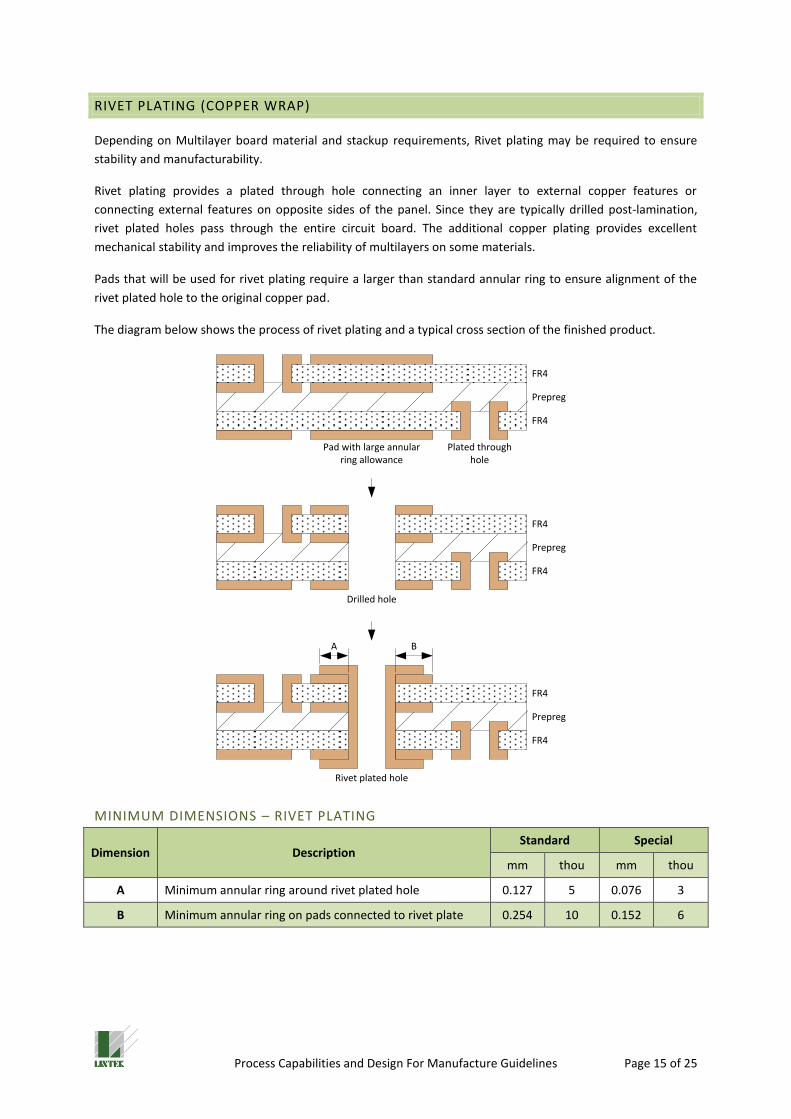
RIVET PLATING (COPPER WRAP)
Depending on Multilayer board material and stackup requirements, Rivet plating may be required to ensure
stability and manufacturability.
Rivet plating provides a plated through hole connecting an inner layer to external copper features or
connecting external features on opposite sides of the panel. Since they are typically drilled post-lamination,
rivet plated holes pass through the entire circuit board. The additional copper plating provides excellent
mechanical stability and improves the reliability of multilayers on some materials.
Pads that will be used for rivet plating require a larger than standard annular ring to ensure alignment of the
rivet plated hole to the original copper pad.
The diagram below shows the process of rivet plating and a typical cross section of the finished product.
FR4
Plated through hole
Prepreg
FR4
Pad with large annular ring allowance
FR4
Prepreg
FR4
Drilled hole
FR4
Prepreg
FR4
Rivet plated hole
BA
MINIMUM DIMENSIONS – RIVET PLATING
Dimension Description Standard Special
mm thou mm thou
A Minimum annular ring around rivet plated hole 0.127 5 0.076 3
B Minimum annular ring on pads connected to rivet plate 0.254 10 0.152 6

Process Capabilities and Design For Manufacture Guidelines Page 16 of 25
INTERNAL POWER AND GROUND PLANES
G
A B
C
D
F
E
MINIMUM DIMENSIONS – POWER AND GROUND PLANES
Dimension Description Standard Special
mm thou mm thou
A Plane to pad 0.2032 8 0.1016 4
B Hole to pad 0.3048 12 0.1016 4
C Plane to track 0.2032 8 0.1016 4
D Track width 0.2032 8 0.1016 4
E Thermal break width 0.3810 15 0.1016 4
F Plane to hole 0.3048 12 0.1905 7.5
G Plane to board edge 0.5080 20 0.1524 6
We encourage designers to add teardrops or signal flares to pads as recommended by IPC 2221 (9.1).
Teardrops increase the reliability of the pad-trace junction and can increase yield in multilayer panels. Lintek
recommends using a teardrop factor of 1.7, as shown below.
Pad radius x 1.7

Process Capabilities and Design For Manufacture Guidelines Page 17 of 25
PTH ASPECT RATIO
Finished HoleDiameter (>¼ t)
Drilled Hole Diameter
Plated Copper Thickness
Material Thickness (t)
Lintek is able to produce plated vias with a standard aspect ratio of 4:1. As such, the drilling diameter of any
plated through hole must be greater than ¼ the thickness of the layer/s it passes through.
For instance, on a 1.60mm thick substrate, the minimum drilling diameter is 0.4mm. This will provide a 0.33mm
finished hole, assuming one ounce (35um) of copper plating.
For applications where an aspect ratio of greater than 4:1 is required, please contact [email protected] to
discuss possible options.
Process Capabilities and Design For Manufacture Guidelines Page 18 of 25
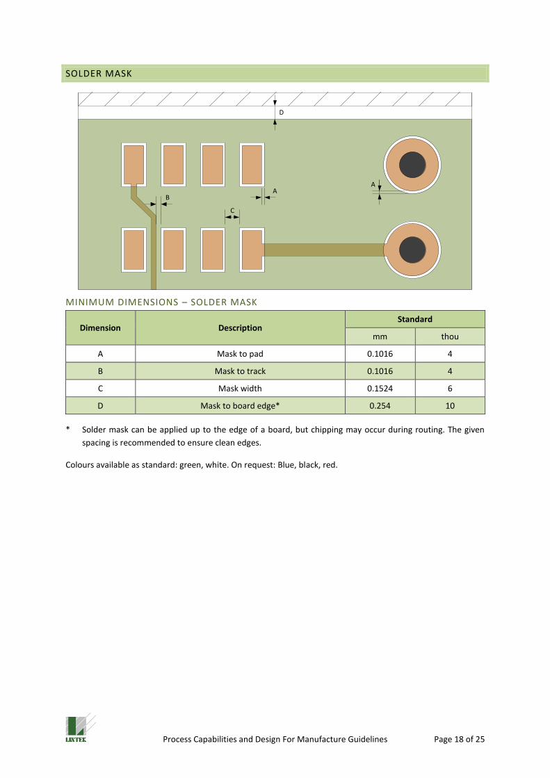
SOLDER MASK
D
AA
C
B
MINIMUM DIMENSIONS – SOLDER MASK
Dimension Description Standard
mm thou
A Mask to pad 0.1016 4
B Mask to track 0.1016 4
C Mask width 0.1524 6
D Mask to board edge* 0.254 10
* Solder mask can be applied up to the edge of a board, but chipping may occur during routing. The given
spacing is recommended to ensure clean edges.
Colours available as standard: green, white. On request: Blue, black, red.

Process Capabilities and Design For Manufacture Guidelines Page 19 of 25
LEGEND
B
AIC23
C5C
MINIMUM DIMENSIONS – LEGEND
Dimension Description Standard
mm thou
A Line width 0.1524 6
B Legend to pad No clearance required.
C Legend to hole No clearance required.
Colours available as standard: white. On request: Blue, black, red, green.

Process Capabilities and Design For Manufacture Guidelines Page 20 of 25
SURFACE FINISHES
Lintek is able to offer a variety of surface finishes to suit any requirement.
Finish Description Thickness
range (microns)
Hot air solder levelling Levelled with 0° air knives for smoother finish. 25
Electroplated nickel Using a nickel sulfamate process, 99.9% pure nickel provides an abrasion, corrosion and wear resistant finish.
0.5 – 5
Electroplated gold – soft 99.9% pure gold provides a highly solderable, conductive finish. Compatibility is material dependent.
0.1 – 3
Electroplated gold – hard Hardened with cobalt, hard gold provides a high conductivity, abrasion resistant contact finish.
0.1 – 2
Electroplated silver Lower cost than gold, electronics grade electroplated silver provides a bright finish and low contact resistance.
0.1 – 10
Immersion gold A thin, high purity gold finish for wire bonding. 0.05 – 0.15
Immersion silver A thin, low cost, highly solderable finish that is the preferred RoHS finish.
0.1 – 0.2

Process Capabilities and Design For Manufacture Guidelines Page 21 of 25
QUALITY ASSURANCE
We offer several options for quality assurance.
Electrical testing of finished products guarantees the integrity of inner layers and fine tracks. Minimum pad size
for testing is 100 microns, with a minimum pitch of 350 microns. Tests are performed for both continuity and
isolation.
We additionally offer manual inspection, Certificate of Conformance documents and First Articles of Inspection
Reporting. Where required, we will prepare encapsulated coupon for inspection reports to confirm copper and
surface finish plating thickness, etch factor of conductors, and other physical characteristics of the product.
Lintek has IPC A600 certified staff and a trainer on site. All PCBs are manufactured to IPC Class 2 minimum.
Certification is available on request.
Additionally, we are compliant with Quality System AS/NZS ISO 9001:2008. Subject to material and process
constraints, we are able to produce boards with Underwriters Laboratories (UL) Approval (File number
E124884).
MANUFACTURING LEAD TIMES
Regarding delivery, we suggest that our clients consider our standard lead times. Typically small run prototypes
have a faster lead time than full scale production.
Board Type Standard Lead Time (working days)
Prototypes Production
Single sided 5 7
Double sided, with plated through holes 7 10
Multilayer (layer count dependent) 10 12-15
Metal backed 12 15
These lead times are a guide only, and may vary depending on factory conditions. Please contact us for the
latest information and an accurate estimate of our delivery capabilities.
In addition to our standard lead times, we offer a rush service for an additional fee. Contact us for details.

Process Capabilities and Design For Manufacture Guidelines Page 22 of 25
LINTEK MINI PROTOTYPE SERVICE
Lintek’s Mini Prototype service is specifically designed to meet a requirement for a small, very fast turnaround,
single or double sided PCB. Instead of requiring a full sized standard panel for production, we can offer fast
processing and delivery on a 280mm x 200mm panel for $290 + GST.
In order to deliver this product at such a low price, the board design must comply with the restrictions below.
To allow our CAD engineers time to set up each panel before production begins, purchase orders and files must
be received before 9am on a Monday. Production will commence at 9am every Tuesday, and the panels will be
dispatched after 3 working days.
Characteristic Value
PCB file format RS274X or Protel PCB files, multiple designs should be sent as one file
PCB Type Double sided with PTH, double sided with NPTH, or single sided
Material 1.6mm FR4
Usable area 280mm x 200mm
Maximum boards per panel 25
Separation between boards 10mm
Copper thickness 30µm – 50µm
Minimum drill diameter 0.4mm
Minimum router diameter 2.0mm
Minimum track and space width 175µm
Minimum annular ring 200µm (after electroplating)
Solder mask Both sides, green only, minimum of 100µm clearance around pads
Overlay/silkscreen Both sides, white, minimum feature width of 150µm
Board layout Drilled tabs
Finish options HASL(tin/lead) or Immersion Silver
Electrical testing Optional, additional $50 + GST
Shipping Within Australia , $15 + GST

Process Capabilities and Design For Manufacture Guidelines Page 23 of 25
JOB INFORMATION
DRAWINGS
Design drawings should be included with any new design. The drawings should clearly show hole sizes, with
different hole sizes clearly represented to allow quick inspection.
Marked hole diameters are assumed to be finished diameter (after plating) unless otherwise specified.
Drawings should include important mechanical dimensions, including overall board dimensions, slots, cut outs
and notches.
The following specifications should also be provided, either on the design drawing or in a separate file:
• board material
• board thickness
• copper plating thickness
• surface finish
• solder mask colour
• legend colour
• quality assurance requirements such as coupons, first article of inspection, bare board testing
• for multilayer boards – copper thickness of internal layers, materials and layup
DESIGN FILES
Preferred format for design files is Protel.pcb format. We support files generated by any software up to Altium
Designer 13.
Gerber files are also accepted, but a specification of the file format is required, including:
• data format
• imperial/metric
• absolute/incremental position coordinates
• character encoding
Gerber files should be provided with a corresponding drill file in Excellon format with:
• ASCII character encoding
• absolute position coordinates
• 2,4 Imperial
• omit trailing zeros
Gerber files are to be identified using the standard Altium/Protel extensions.
Extension Layer Description
GBL Bottom layer Copper layer
GBO Bottom overlay Overlay, silkscreen, legend
GBP Bottom paste Solder paste for SMD assembly (not offered by Lintek)
GBS Bottom soldermask Solder mask, solder resist
GKO Keep out Areas for copper exclusion

Process Capabilities and Design For Manufacture Guidelines Page 24 of 25
Extension Layer Description
GM1, GM2.. Mechanical 1, 2.. Mechanical layers
G1, G2.. Midlayer 1, 2.. Internal copper signal layers
GP1, GP2.. Plane 1, 2.. Internal planes for power and ground
GPB Pads Bottom Unused
GPT Pads Top Unused
GTL Top Layer Copper layer
GTO Top Overlay Overlay, silkscreen, legend
GTP Top Paste Solder paste for SMD assembly (not offered by Lintek)
GTS Top Soldermask Solder mask, solder resist
Multiple designs are to be sent as a single PCB file.
Include outlines and cutouts on mechanical layer 1.
Multilayer boards should include a text document indicating the layup order.

Process Capabilities and Design For Manufacture Guidelines Page 25 of 25
APPENDIX 1 – PROCESS COMPARISON
Etched laminate
Metallising
Copper panel plating
Electroplated tin
50µm heavy etch
Tin strip
2-3µm microetch
Electroplated copper
Photoresist strip
Plating resist film
2µm metallised copper 0.4µm electroless copper
5µm copper panel plating
50µm resist film 38µm resist film
25µm electrodeposited copper45µm electrodeposited copper
3µm electrodeposited tin (etch resist)
No undercut
Undercut in copper
Varying copper thickness results in weak points
Final Etch
Bulk etching
Electroless copper plating
Lintek Other PCB manufacturers
Drilling
Drilledhole
18µm copper clad laminate
Conditioner
Microetch
Initiator


![1'cc]]nica] (;ll:tl.:~cte]”istics and AccuIacy Cnpal)ilities of Delta l](https://img.pdfslide.net/doc/110x75/589d98d01a28ab6d4a8bc1c1/1ccnica-lltlcteistics-and-accuiacy-cnpalilities-of-delta-l-.jpg)