Embed Size (px)
Citation preview
Doc.Nr. 8281000.8
Product Family Specification
CMA3000-D0X Series 3-axis accelerometer
CMA3000-D0X Series
VTI Technologies Oy PRELIMINARY - Subject to changes 2/ 34 www.vti.fi Doc.Nr. 8281000.8 Rev. 0.8
TABLE OF CONTENTS
1 General Description ............................................................................................................. 5
1.1 Introduction................................................................................................................................5 1.2 Functional Description ..............................................................................................................5
1.2.1 Sensing element..................................................................................................................5 1.2.2 Interface IC...........................................................................................................................5 1.2.3 Factory calibration ..............................................................................................................5 1.2.4 Supported features .............................................................................................................6 1.2.5 Operation modes.................................................................................................................6
1.2.5.1 Power Down .................................................................................................................................6 1.2.5.2 Measurement................................................................................................................................6 1.2.5.3 Motion Detection..........................................................................................................................6 1.2.5.4 Free-Fall Detection ......................................................................................................................6
1.2.6 Interrupt................................................................................................................................6 1.2.7 Operational flow chart ........................................................................................................7
2 Reset and power up, Operation Modes, HW functions and Clock................................... 8
2.1 Reset and power up...................................................................................................................8 2.2 Power Down mode.....................................................................................................................8 2.3 Measurement Mode ...................................................................................................................8
2.3.1 Description...........................................................................................................................8 2.3.2 Usage....................................................................................................................................8
2.4 Motion Detection Mode .............................................................................................................8 2.4.1 Description...........................................................................................................................8 2.4.2 Usage....................................................................................................................................9 2.4.3 Example..............................................................................................................................10
2.5 Free-Fall Detection...................................................................................................................10 2.5.1 Description.........................................................................................................................10 2.5.2 Usage..................................................................................................................................10 2.5.3 Example..............................................................................................................................10
2.6 Interrupt function (INT-pin) .....................................................................................................11 2.6.1 Usage..................................................................................................................................11
2.7 Clock .........................................................................................................................................11
3 Addressing Space.............................................................................................................. 12
3.1 Register Description................................................................................................................12 3.2 Non-volatile memory ...............................................................................................................12 3.3 Registers...................................................................................................................................12
4 Serial Interfaces ................................................................................................................. 17
4.1 SPI Interface .............................................................................................................................17
CMA3000-D0X Series
VTI Technologies Oy PRELIMINARY - Subject to changes 3/ 34 www.vti.fi Doc.Nr. 8281000.8 Rev. 0.8
4.1.1 SPI frame format................................................................................................................17 4.1.2 Examples of SPI communication.....................................................................................18
4.1.2.1 Example of register read...........................................................................................................18 4.1.3 Multiple slave devices in SPI bus ....................................................................................18
4.2 I2C Interface ..............................................................................................................................19 4.2.1 I2C frame format.................................................................................................................19
4.2.1.1 I2C write mode............................................................................................................................19 4.2.1.2 I2C read mode.............................................................................................................................19
4.2.2 Examples of I2C communication......................................................................................19
5 Electrical Characteristics .................................................................................................. 20
5.1 Absolute maximum ratings.....................................................................................................20 5.2 Power Supply ...........................................................................................................................20 5.3 Digital I/O Specification...........................................................................................................20
5.3.1 Digital I/O DC characteristics ...........................................................................................20 5.3.2 Digital I/O level shifter.......................................................................................................20 5.3.3 SPI AC characteristics ......................................................................................................21 5.3.4 I2C AC characteristics .......................................................................................................21
6 Package Characteristics.................................................................................................... 22
6.1 Dimensions...............................................................................................................................22
7 Application information ..................................................................................................... 23
7.1 Pin Description.........................................................................................................................23 7.2 Recommended circuit diagram ..............................................................................................23 7.3 Recommended PWB layout ....................................................................................................24 7.4 Assembly instructions ............................................................................................................24 7.5 Tape and reel specifications...................................................................................................24
8 Data sheet references ........................................................................................................ 25
8.1 Offset.........................................................................................................................................25 8.1.1 Offset calibration error .....................................................................................................25 8.1.2 Offset temperature error...................................................................................................25
8.2 Sensitivity.................................................................................................................................25 8.2.1 Sensitivity calibration error..............................................................................................26 8.2.2 Sensitivity temperature error ...........................................................................................26
8.3 Linearity ....................................................................................................................................26 8.4 Noise .........................................................................................................................................27 8.5 Bandwidth.................................................................................................................................28 8.6 Cross-axis sensitivity ..............................................................................................................28 8.7 Turn-on time.............................................................................................................................29
CMA3000-D0X Series
VTI Technologies Oy PRELIMINARY - Subject to changes 4/ 34 www.vti.fi Doc.Nr. 8281000.8 Rev. 0.8
9 Known issues ..................................................................................................................... 30
9.1 Acceleration data reading via I2C bus....................................................................................30 9.1.1 Interrupt based acceleration reading ..............................................................................30 9.1.2 Acceleration reading without interrupts .........................................................................31
9.2 Leakage current when VDD - DVIO > 0.3 V............................................................................31 9.3 Sensing element's bandwidth is lower than the target ........................................................31
10 Order Information............................................................................................................... 32
11 Document Change Control................................................................................................ 33
12 Contact Information ........................................................................................................... 34
CMA3000-D0X Series
VTI Technologies Oy PRELIMINARY - Subject to changes 5/ 34 www.vti.fi Doc.Nr. 8281000.8 Rev. 0.8
1 General Description 1.1 Introduction
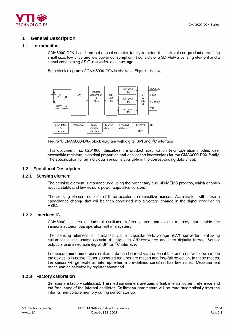
CMA3000-D0X is a three axis accelerometer family targeted for high volume products requiring small size, low price and low power consumption. It consists of a 3D-MEMS sensing element and a signal conditioning ASIC in a wafer level package. Both block diagram of CMA3000-D0X is shown in Figure 1 below.
DE-MUX1:3
Oscillator &
clock
Motion detector
Free fall detector
Reference
CSB
Control &
INT
C/V
Analog
calibration &
ADC
Non-Volatile Memory
Low-pass Filter
Low-pass Filter
Low-pass Filter
SCK/SCL
MISO
MOSI/SDA
SPI &
I2C i/f
INT
Figure 1. CMA3000-D0X block diagram with digital SPI and I2C interface This document, no. 8281000, describes the product specification (e.g. operation modes, user accessible registers, electrical properties and application information) for the CMA3000-D0X family. The specification for an individual sensor is available in the corresponding data sheet.
1.2 Functional Description 1.2.1 Sensing element
The sensing element is manufactured using the proprietary bulk 3D-MEMS process, which enables robust, stable and low noise & power capacitive sensors. The sensing element consists of three acceleration sensitive masses. Acceleration will cause a capacitance change that will be then converted into a voltage change in the signal conditioning ASIC.
1.2.2 Interface IC CMA3000 includes an internal oscillator, reference and non-volatile memory that enable the sensor's autonomous operation within a system. The sensing element is interfaced via a capacitance-to-voltage (CV) converter. Following calibration in the analog domain, the signal is A/D-converted and then digitally filtered. Sensor output is user selectable digital SPI or I2C interface. In measurement mode acceleration data can be read via the serial bus and in power down mode the device is in-active. Other supported features are motion and free-fall detection. In these modes, the sensor will generate an interrupt when a pre-defined condition has been met. Measurement range can be selected by register command.
1.2.3 Factory calibration Sensors are factory calibrated. Trimmed parameters are gain, offset, internal current reference and the frequency of the internal oscillator. Calibration parameters will be read automatically from the internal non-volatile memory during sensor startup.
CMA3000-D0X Series
VTI Technologies Oy PRELIMINARY - Subject to changes 6/ 34 www.vti.fi Doc.Nr. 8281000.8 Rev. 0.8
1.2.4 Supported features
Supported features are listed in Table 1 below.
Table 1. CMA3000-D0X devices’ summary.
Features CMA3000-D01 Supply voltage 1.7 V – 3.6 V I/O voltage 1.7 V – 3.6 V Measuring range (selectable) ±2 g, ±8 g Resolution (2g /8g range) 17 mg / 67 mg Sensitivity (2g /8g range) 56 counts/g / 14 counts/g Motion detection User enabled Free fall detection User enabled Interface SPI max 500 kHz, I2C fast mode 400 kHz Clock Internal
1.2.5 Operation modes
1.2.5.1 Power Down
In Power Down (PD) mode device's volatile register keep their contents and the current consumption is minimized. Power down mode is the default mode after start up.
1.2.5.2 Measurement
In Measurement mode (Meas) the sensor offers acceleration information via the digital SPI/I2C interface. Interrupt can be activated via INT-pin, when each xyz-acceleration sample are ready to be read. Measurement range and sample rate are user selectable according to Table 2. Measurement mode can be activated by detected motion.
1.2.5.3 Motion Detection
Motion Detection (MD) mode is intended to be used to save system level power consumption. In this mode, CMA3000-D0X activates the interrupt via the INT-pin when motion is detected. Motion sensitivity level can be configured via the SPI or I2C bus. Moreover, the duration of the motion to be detected can be user defined. Once the interrupt has happened, the detected direction can be read out from the corresponding status register. Low sample rate (10 Hz) band-pass filtered acceleration information is available in MD mode. The device can be configured to switch automatically into the measurement mode with highest sampling rate after motion detection.
1.2.5.4 Free-Fall Detection
Free-Fall Detection (FFD) is intended to be used to save system resources. This feature activates the interrupt via the INT-pin when free-fall is detected. Acceleration information is available when the FFD is enabled.
1.2.6 Interrupt The CMA3000 has a dedicated output pin (INT) to be used as the interrupt for the master controller. Interrupt conditions can be activated and deactivated via the SPI or I2C bus. Once the interrupt has happened, the interrupt source can be read out from the corresponding status register.

CMA3000-D0X Series
VTI Technologies Oy PRELIMINARY - Subject to changes 7/ 34 www.vti.fi Doc.Nr. 8281000.8 Rev. 0.8
1.2.7 Operational flow chart
CMA3000 power up
Figure 2. CMA3000 operational flow chart.
CMA3000 in power down mode
Activate CMA3000 operation mode via SPI/I2C bus
CMA3000 operation in application
CMA3000 power down mode can be activated via SPI/I2C bus
CMA3000 operation mode can be changed via SPI/I2C bus
Measurement mode Free fall mode Motion detection mode
Low pass filtered XYZ acceleration data available
Low pass filtered XYZ acceleration data available
Band pass filtered XYZ acceleration data available
Ranges and data rates: 2g: 400Hz, 100Hz
8g: 400Hz, 100Hz, 40Hz
INT-pin gives interrupt when free fall is detected
Ranges and data rates: Ranges and data rates: 8g: 10Hz 2g: 400Hz, 100Hz
8g: 400Hz, 100Hz
INT-pin gives interrupt when motion is detected
INT-pin gives interrupt when new data is available
Additional configuration option: Additional configuration option: Additional configuration option: • Motion detection trigger conditions
can be configured (time & acceleration)
• INT-pin data ready functionality can be disabled
• Free fall trigger conditions can be configured (time & acceleration)
• CMA3000 can be configured to switch to measurement mode with
400Hz output data rate after motion is detected
CMA3000-D0X Series
VTI Technologies Oy PRELIMINARY - Subject to changes 8/ 34 www.vti.fi Doc.Nr. 8281000.8 Rev. 0.8
2 Reset and power up, Operation Modes, HW functions and Clock 2.1 Reset and power up
The CMA3000 has internal power-on reset circuit. It releases the internal reset-signal once the power supplies will be within the specified range. After releasing the internal reset, the CMA3000 will read configuration and calibration data from the non-volatile memory to volatile registers. Then the CMA3000 will make parity check to the read memory content. The STATUS register's PERR-bit="0" shows successful memory read operation. Device can be externally reset by writing the sequence 02h, 0Ah, 04h into the RSTR-register.
2.2 Power Down mode The CMA3000-D0X enters the power down mode by default after power-on reset and initialization of the volatile registers. PD can also be set by writing MODE[2:0]=000b (or MODE[2:0]=111b) to CTRL register. Output registers will keep their content in the power down mode.
2.3 Measurement Mode 2.3.1 Description
The CMA3000-D0X enters the measurement mode by writing MODE[2:0]=0XXb to CTRL register. Data will be reliable in the output registers after the product specific turn-on time. Default sample rate is 400 Hz (MODE[2:0]=010b). Other data rates are 100 Hz (MODE[2:0]=001b) and 40 Hz (MODE[2:0]=011b). Table 2. CMA3000-D0X measurement ranges and output sample rates Measurement range Output sample rates 2 g 400 Hz, 100 Hz 8 g 400 Hz, 100 Hz, 40 Hz INT-pin gives an interrupt by default when new data is available.
2.3.2 Usage Acceleration data can be read from data output registers DOUTX, DOUTY and DOUTZ. See section 2.6 for INT-pin configuration details.
2.4 Motion Detection Mode 2.4.1 Description
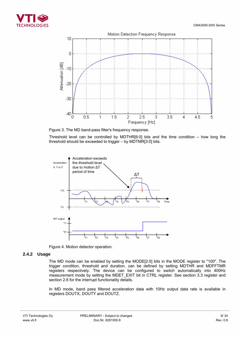
In MD mode the device works at 10 Hz sample rate and the fixed measurement range is 8 g. Signal is band pass filtered and fed to threshold level programmable digital comparator and a configurable trigger function. Filtered signal is also available at output registers. The device can be configured to switch automatically into the measurement mode with highest sampling rate (400Hz) after motion is detected. The used measurement range will be defined by G_RANGE bit. Nominal BPF's -3 dB high-pass frequency is 1.3 Hz and -3 dB low-pass frequency is 3.8 Hz. See Figure 3 below.
CMA3000-D0X Series
VTI Technologies Oy PRELIMINARY - Subject to changes 9/ 34 www.vti.fi Doc.Nr. 8281000.8 Rev. 0.8
Figure 3. The MD band-pass filter's frequency response.
Threshold level can be controlled by MDTHR[6:0] bits and the time condition – how long the threshold should be exceeded to trigger – by MDTMR[3:0] bits.
∆T
+TL
Acceleration exceeds the threshold level due to motion ∆T period of time
-TL
Acceleration
X, Y or Z
T1 T2 T3 T4 T5 T6 T7 T8 Time
T1 T2 T3 T4 T5 T6 T7 T8
INT output
"1"
"0"
Figure 4. Motion detector operation.
2.4.2 Usage The MD mode can be enabled by setting the MODE[2:0] bits in the MODE register to "100". The trigger condition, threshold and duration, can be defined by setting MDTHR and MDFFTMR registers respectively. The device can be configured to switch automatically into 400Hz measurement mode by setting the MDET_EXIT bit in CTRL register. See section 3.3 register and section 2.6 for the interrupt functionality details. In MD mode, band pass filtered acceleration data with 10Hz output data rate is available in registers DOUTX, DOUTY and DOUTZ.

CMA3000-D0X Series
VTI Technologies Oy PRELIMINARY - Subject to changes 10/ 34 www.vti.fi Doc.Nr. 8281000.8 Rev. 0.8
2.4.3 Example Below is a simple example of motion detection usage:
1. Write "00001000" (08h) into the MODE register (enable motion detection mode, MODE[2:0] bits = '100').
2. Band pass filtered acceleration data at 10 Hz sample rate is available at the output registers.
3. The INT-pin is activated when motion is detected; see section 2.6 for detailed INT-pin information.
2.5 Free-Fall Detection 2.5.1 Description
During free-fall in the gravitation field, all 3 orthogonal acceleration components are ideally equal to zero. Due to practical non-idealities, detection must be done using Threshold Level (TL) greater than 0. When enabled, the Free-Fall Detection (FFD) will monitor the measured acceleration in the X, Y and Z directions. If all measured XYZ acceleration values stay within the TL longer than time TFF (Figure 5 below), the FFD will generate an interrupt to the INT-pin. TL can be controlled by FFTHR [6:0] and TFF by FFTMR [3:0] bits.
T1 T2 T3 T4 T5 T6 T7 T8
+TL
TFF
-TL
Acceleration
X, Y and Z
Time
T1 T2 T3 T4 T5 T6 T7 T8 Time
INT output
"1"
"0"
Figure 5. Free Fall condition.
2.5.2 Usage Free-fall detection can be enabled by setting MODE[2:0] bits in the CTRL register to "101" (sample rate 100 Hz) or to "110" (sample rate 400 Hz). See section 3.3 for MODE register details. Acceleration data is available in registers DOUTX, DOUTY and DOUTZ as in measurement mode. See section 3.3 for output register and section 2.6 for interrupt functionality details.
2.5.3 Example Below is a simple example of free-fall detection usage:
1. Write "00001100" (0Ch) into the MODE register (enable 400 Hz free fall detection mode, MODE[2:0] bits = '110').
2. Acceleration data can be read normally
CMA3000-D0X Series
VTI Technologies Oy PRELIMINARY - Subject to changes 11/ 34 www.vti.fi Doc.Nr. 8281000.8 Rev. 0.8
3. INT-pin is activated when free fall is detected. See section 2.6 for detailed INT-pin information.
2.6 Interrupt function (INT-pin) 2.6.1 Usage
Depending on the CMA3000 operational configuration, the INT-pin can give an interrupt in following cases:
1. Normal measurement mode: INT-pin gives interrupt when new data is available 2. Free fall detection mode: INT-pin gives an interrupt to signal that free fall is detected 3. Motion detection mode: INT-pin gives an interrupt to signal that motion is detected
The interrupt polarity (active high/low) can be configured with CTRL register's INT_LEVEL bit. If the CMA3000 is in normal measurement mode, the INT pin is automatically cleared by reading the acceleration output data. INT-pin data ready functionality can be disabled by setting the CTRL register's INT_DIS bit. If INT-pin gives an interrupt in free fall or motion detection mode, the INT_STATUS register must be read to acknowledge and clear the interrupt. In motion detection mode the INT_STATUS register content gives information of which XYZ directions have exceed the trigger conditions. See section 3.3 for CTRL and INT_STATUS register details.
2.7 Clock The CMA3000 has an internal factory trimmed oscillator and clock generator. Internal frequencies vary product by product.
CMA3000-D0X Series
VTI Technologies Oy PRELIMINARY - Subject to changes 12/ 34 www.vti.fi Doc.Nr. 8281000.8 Rev. 0.8
3 Addressing Space The CMA3000 register contents and bit definitions are described in more detail in the following sections.
3.1 Register Description The CMA3000 addressing space is presented in Table 3 below.
Table 3. List of registers.
Addr. Name Description Mode (R, RW, NV)
Reg. type
00h WHO_AM_I Identification register R Output 01h REVID ASIC revision ID, fixed in metal R Output 02h CTRL Configuration (por, operation
modes) RW Conf
03h STATUS Status (por, EEPROM parity) R Output 04h RSTR Reset Register RW Conf 05h INT_STATUS Interrupt status register R Output 06h DOUTX X channel output data register R Output 07h DOUTY Y channel output data register R Output 08h DOUTZ Z channel output data register R Output 09h MDTHR Motion detection threshold value
register RW Conf
0Ah MDFFTMR Free fall and motion detection time register
RW Conf
0Bh FFTHR Free fall threshold value register RW Conf 0Ch I2C_ADDR I2C device address R Conf
0Dh-19h Reserved Add. is the register address in hex format. RW – Read / Write register, R – Read-only register, NV – non-volatile register content.
3.2 Non-volatile memory The CMA3000 has an internal non-volatile memory for calibration and configuration data. Memory content will be programmed during production and is not user configurable. Initial configuration values mirrored to volatile registers after reset can be found in the following section 3.3.
3.3 Registers Address: 00h Register name: WHO_AM_I, Identification register
Bits Mode Initial Value Name Description
7 R 0 Reserved 6:0 R TBD Identification register
Address: 01h Register name: REVID, ASIC revision ID
Bits Mode Initial Value Name Description
7:4 R TBD REVMAJ Major revision number 3:0 R TBD REVMIN Minor revision number (metal mask change)
CMA3000-D0X Series
VTI Technologies Oy PRELIMINARY - Subject to changes 13/ 34 www.vti.fi Doc.Nr. 8281000.8 Rev. 0.8
Address: 02h Register name: CTRL, Control register
Bits Mode Initial Value Name Description
7 RW 0 G_RANGE 0 – 8g measurement range is selected 1 – 2g measurement range is selected
6 RW 0 INT_LEVEL 0 – INT is active when INT pin is set to logic high 1 – INT is active when INT pin is set to logic low
5 RW 0 MDET_EXIT 0 – Device goes to measurement mode after motion is detected (400Hz ODR) 1 – Device remains in motion detection mode after motion is detected.
4 RW 0 I2C_DIS 0 – I2C interface enabled 1 – I2C interface disabled.
3:1 RW 0 MODE[2:0] 000 – Power down mode, default mode. 001 – Measurement mode, 100 Hz ODR. 010 – Measurement mode, 400 Hz ODR. 011 – Measurement mode, 40 Hz ODR. 100 – Motion detection mode, 10 Hz ODR. 101 – Free fall detection mode, 100 Hz ODR. 110 – Free fall detection mode, 400 Hz ODR. 111 – Power down mode
0 RW 0 INT_DIS 0 – Interrupts enabled • Measurement mode: data ready • Motion detection mode: motion detected • Free fall detection mode: free fall detected
1 – Interrupts disabled Note that after changing MODE bits it may take some time to recover the target operating state. ODR = Output Data Rate. Address: 03h Register name: STATUS, Status register
Bits Mode Initial Value Name Description
7:4 0000 Reserved 3 R 0 PORST 1 means Power-on-Reset state. Reading the register
sets always bit to 0. 2:1 00 Reserved 0 R 0 PERR 0 – No EEPROM Parity Error
1 – EEPROM Parity Error Address: 04h Register name: RSTR, Reset register
Bits Mode Initial Value Name Description
7:0 RW 00h RSTR Writing 02h, 0Ah, 04h in this order resets ASIC. Other sequences reserved.

CMA3000-D0X Series
VTI Technologies Oy PRELIMINARY - Subject to changes 14/ 34 www.vti.fi Doc.Nr. 8281000.8 Rev. 0.8
Address: 05h Register name: INT_STATUS, Interrupt status register
Bits Mode Initial Value Name Description
7:3 TBD Reserved 2 R 0 FFDET 1 – Free fall detected (i.e. 0 g acceleration)
0 – Free fall not detected 1:0 R 00 MDET 00 – No motion detected
01 – Trigger on X-axis 10 – Trigger on Y-axis 11 – Trigger on Z-axis
Note: Contents of INT_STATUS [2:0] is set to '000' always after reading of this register. Address: 06h Register name: DOUTX, X-channel output register
Bits Mode Initial Value Name Description
7:0 R 00h DOUTX See SPI data frame description for more info. Address: 07h Register name: DOUTY, Y-channel output register
Bits Mode Initial Value Name Description
7:0 R 00h DOUTY See SPI data frame description for more info. Address: 08h Register name: DOUTZ, Z-channel output register
Bits Mode Initial Value Name Description
7:0 R 00h DOUTZ See SPI data frame description for more info. The bit level description for acceleration data from DOUTX ... DOUTZ registers is presented in Table 4 below. The acceleration data is presented in 2's complement format. At 0 g acceleration the output is ideally 00h.
Table 4. Bit level description in [mg] for acceleration registers of CMA3000-D01.
Range G_RANGE Output sample rate B7 B6 B5 B4 B3 B2 B1 B0
2g 1 400 Hz, 100 Hz s 1142 571 286 143 71 36 1/56 = 18 mg2g 1 40 Hz, 10 Hz s 4571 2286 1142 571 286 143 1/14 = 71 mg8g 0 400 Hz, 100 Hz s 4571 2286 1142 571 286 143 1/14 = 71 mg8g 0 40 Hz, 10 Hz s 4571 2286 1142 571 286 143 1/14 = 71 mg
s = sign bit

CMA3000-D0X Series
VTI Technologies Oy PRELIMINARY - Subject to changes 15/ 34 www.vti.fi Doc.Nr. 8281000.8 Rev. 0.8
Address: 09h Register name: MDTHR, Motion detection threshold value register
Bits Mode Initial Value Name Description
7 0 Reserved 6:0 RW 08h MDTHR[6:0] Motion detection threshold level absolute value. See
detailed bit level weighting in Table 5 (bits [6:0])
Table 5. Bit level description in [mg] for motion detection threshold of CMA3000-D01.
Range G_RANGE B7 B6 B5 B4 B3 B2 B1 B0 2g 1 x 1142 571 286 143 71 36 1/56 = 18 mg8g 0 x 4571 2286 1142 571 286 143 1/14 = 71 mg
x=not used bit Address: 0Ah Register name: MDFFTMR, Motion and free fall detection time register
Bits Mode Initial Value Name Description 7:4 RW 3h MDTMR[3:0] Motion detection timer bits 3:0 RW 3h FFTMR [3:0] Free fall detection timer bits
The LSB bit weighting for MDTMR and FFTMR bits are converted to seconds by using the currently configured CMA3000 output data rate (ODR), as follows:
MDTMRLSB[sec] = 1 / ODR[Hz], and FFTMRLSB[sec] = 1 / ODR[Hz]
Were the ODR is the currently configured CMA3000 output data rate, which is defined by MODE bits (bits [3:1] in CTRL register). An example for CMA3000-D01 timer bit weighting is presented in Table 6 below.
Table 6. An example for CMA3000-D01 MDTMR and FFTMR bit level descriptions in [ms].
Timer MDTMR FFTMR Register bit number B7 B6 B5 B4 B3 B2 B1 B0
Timer bit number
MDTMR b3
MDTMR b2
MDTMR B1
MDTMR b0
FFTMR b3
FFTMR b2
FFTMR B1
FFTMR b0
CMA3000-D01, MODE bits x10 ODR: 400Hz
x x x x 20 10 5 1/400s = 2,5 ms
CMA3000-D01, MODE bits x01 ODR: 100Hz
x x x x 80 40 20 1/100s = 10 ms
CMA3000-D01, MODE bits 100 ODR: 10Hz
x 400 200 1/10s = 100 ms x x x x
x=not used bit
CMA3000-D0X Series
VTI Technologies Oy PRELIMINARY - Subject to changes 16/ 34 www.vti.fi Doc.Nr. 8281000.8 Rev. 0.8
Address: 0Bh Register name: FFTHR, Free fall threshold value register
Bits Mode Initial Value Name Description
7:5 000 Reserved, write these bits to '000' 4:0 RW 08h FFTHR[5:0] Free fall detection threshold level absolute value. See
detailed bit level weighting in Table 7 below.
Table 7. Bit level description in [mg] for free fall detection threshold of CMA3000-D01.
Range G_RANGE B4 B3 B2 B1 B0 2g 1 71 36 1/60=17 mg x x 8g 0 1142 571 286 143 1/14 = 71 mg
x=not used bit Address: 0Ch Register name: I2C_ADDR, Device address for I2C bus
Bits Mode Initial Value Name Description
7 0 Reserved 6:0 RW 1Ch ADDR[6:0] 7-bit device address for I2C bus. Register content is
non-volatile.
CMA3000-D0X Series
VTI Technologies Oy PRELIMINARY - Subject to changes 17/ 34 www.vti.fi Doc.Nr. 8281000.8 Rev. 0.8
4 Serial Interfaces Communication between the CMA3000 sensor and master controller is based on serial data transfer and a dedicated interrupt line (INT-pin). Two different serial interfaces are available for the CMA3000 sensor: SPI and I2C (Phillips specification V2.1). Selection between these two interfaces is done using the chip select signal. The I2C interface can be also disabled by re-configuring a register content. The CMA3000 acts as a slave on both the SPI and I2C bus.
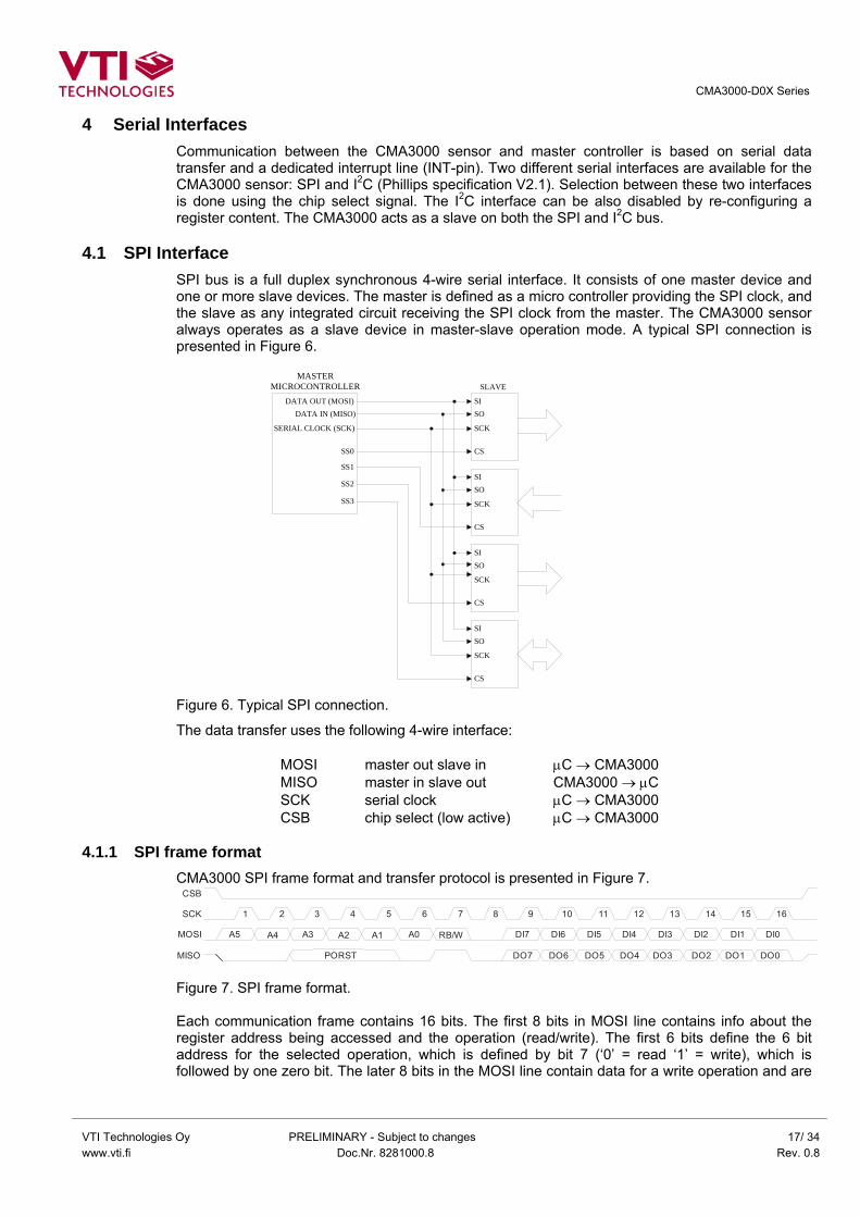
4.1 SPI Interface SPI bus is a full duplex synchronous 4-wire serial interface. It consists of one master device and one or more slave devices. The master is defined as a micro controller providing the SPI clock, and the slave as any integrated circuit receiving the SPI clock from the master. The CMA3000 sensor always operates as a slave device in master-slave operation mode. A typical SPI connection is presented in Figure 6.
DATA OUT (MOSI)DATA IN (MISO)
SERIAL CLOCK (SCK)
SS0
SS1
SS2
SS3
MASTERMICROCONTROLLER
SISO
SCK
CS
SLAVE
SISO
SCK
CS
SISO
SCK
CS
SISO
SCK
CS Figure 6. Typical SPI connection.
The data transfer uses the following 4-wire interface:
MOSI master out slave in µC → CMA3000 MISO master in slave out CMA3000 → µC SCK serial clock µC → CMA3000 CSB chip select (low active) µC → CMA3000
4.1.1 SPI frame format
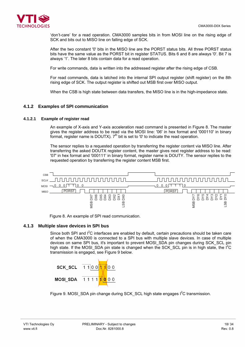
CMA3000 SPI frame format and transfer protocol is presented in Figure 7.
MOSI
MISO
RB/WA5 A4 A3 A2 A1 A0 DI7 DI6 DI5 DI4 DI3 DI2 DI1 DI0
DO7 DO6 DO5 DO4 DO3 DO2 DO1 DO0
SCK
CSB
PORST
1 2 3 4 5 6 7 8 9 10 11 12 13 14 15 16
Figure 7. SPI frame format. Each communication frame contains 16 bits. The first 8 bits in MOSI line contains info about the register address being accessed and the operation (read/write). The first 6 bits define the 6 bit address for the selected operation, which is defined by bit 7 (‘0’ = read ‘1’ = write), which is followed by one zero bit. The later 8 bits in the MOSI line contain data for a write operation and are
CMA3000-D0X Series
VTI Technologies Oy PRELIMINARY - Subject to changes 18/ 34 www.vti.fi Doc.Nr. 8281000.8 Rev. 0.8
‘don’t-care’ for a read operation. CMA3000 samples bits in from MOSI line on the rising edge of SCK and bits out to MISO line on falling edge of SCK. After the two constant '0' bits in the MISO line are the PORST status bits. All three PORST status bits have the same value as the PORST bit in register STATUS. Bits 6 and 8 are always '0'. Bit 7 is always ‘1’. The later 8 bits contain data for a read operation. For write commands, data is written into the addressed register after the rising edge of CSB. For read commands, data is latched into the internal SPI output register (shift register) on the 8th rising edge of SCK. The output register is shifted out MSB first over MISO output. When the CSB is high state between data transfers, the MISO line is in the high-impedance state.
4.1.2 Examples of SPI communication
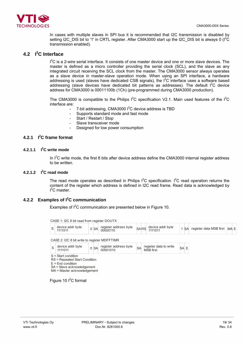
4.1.2.1 Example of register read
An example of X-axis and Y-axis acceleration read command is presented in Figure 8. The master gives the register address to be read via the MOSI line: '06' in hex format and '000110' in binary format, register name is DOUTX). 7th bit is set to '0' to indicate the read operation. The sensor replies to a requested operation by transferring the register content via MISO line. After transferring the asked DOUTX register content, the master gives next register address to be read: '07' in hex format and '000111' in binary format, register name is DOUTY. The sensor replies to the requested operation by transferring the register content MSB first.
MOSI
MISO
SCLK
CSB
0 0 0 0 01 1 0 0 0 01 1 1
MS
B D
X7D
X6D
X5D
X4D
X3D
X2 DX
1LS
B D
X0
PORSTM
SB D
Y7
DY
6D
Y5
DY4
DY
3D
Y2 DY1
LSB
DY0
PORST
Figure 8. An example of SPI read communication.
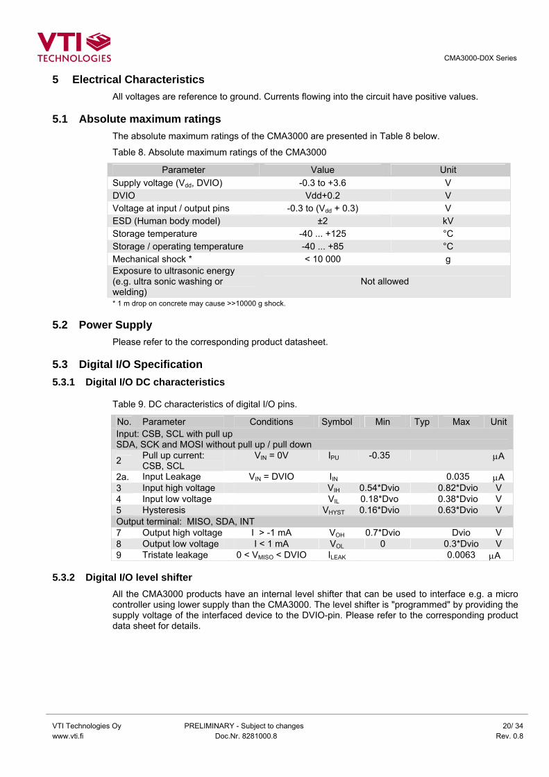
4.1.3 Multiple slave devices in SPI bus Since both SPI and I2C interfaces are enabled by default, certain precautions should be taken care of when the CMA3000 is connected to a SPI bus with multiple slave devices. In case of multiple devices on same SPI bus, it's important to prevent MOSI_SDA pin changes during SCK_SCL pin high state. If the MOSI_SDA pin state is changed when the SCK_SCL pin is in high state, the I2C transmission is engaged, see Figure 9 below.
Figure 9. MOSI_SDA pin change during SCK_SCL high state engages I2C transmission.
CMA3000-D0X Series
VTI Technologies Oy PRELIMINARY - Subject to changes 19/ 34 www.vti.fi Doc.Nr. 8281000.8 Rev. 0.8
In cases with multiple slaves in SPI bus it is recommended that I2C transmission is disabled by setting I2C_DIS bit to '1' in CRTL register. After CMA3000 start up the I2C_DIS bit is always 0 (I2C transmission enabled).
4.2 I2C Interface I2C is a 2-wire serial interface. It consists of one master device and one or more slave devices. The master is defined as a micro controller providing the serial clock (SCL), and the slave as any integrated circuit receiving the SCL clock from the master. The CMA3000 sensor always operates as a slave device in master-slave operation mode. When using an SPI interface, a hardware addressing is used (slaves have dedicated CSB signals), the I2C interface uses a software based addressing (slave devices have dedicated bit patterns as addresses). The default I2C device address for CMA3000 is 00011100b (1Ch) (pre-programmed during CMA3000 production). The CMA3000 is compatible to the Philips I2C specification V2.1. Main used features of the I2C interface are:
- 7-bit addressing, CMA3000 I2C device address is TBD - Supports standard mode and fast mode - Start / Restart / Stop - Slave transceiver mode - Designed for low power consumption
4.2.1 I2C frame format
4.2.1.1 I2C write mode
In I2C write mode, the first 8 bits after device address define the CMA3000 internal register address to be written.
4.2.1.2 I2C read mode
The read mode operates as described in Philips I2C specification. I2C read operation returns the content of the register which address is defined in I2C read frame. Read data is acknowledged by I2C master.
4.2.2 Examples of I2C communication
Examples of I2C communication are presented below in Figure 10.
S device addr byte1111011 0 SA SA RS 1 SA MA Eregister address byte
00000110device addr byte1111011 register data MSB first
S device addr byte1111011 0 SA SA SA Eregister address byte
00001010register data to writeMSB first
CASE 1: I2C 8 bit read from register DOUTX
CASE 2: I2C 8 bit write to register MDFFTIMR
S = Start conditionRS = Repeated Start ConditionE = End conditionSA = Slave acknowledgementMA = Master acknowledgement
Figure 10 I2C format
CMA3000-D0X Series
VTI Technologies Oy PRELIMINARY - Subject to changes 20/ 34 www.vti.fi Doc.Nr. 8281000.8 Rev. 0.8
5 Electrical Characteristics All voltages are reference to ground. Currents flowing into the circuit have positive values.
5.1 Absolute maximum ratings The absolute maximum ratings of the CMA3000 are presented in Table 8 below.
Table 8. Absolute maximum ratings of the CMA3000
Parameter Value Unit Supply voltage (Vdd, DVIO) -0.3 to +3.6 V DVIO Vdd+0.2 V Voltage at input / output pins -0.3 to (Vdd + 0.3) V ESD (Human body model) ±2 kV Storage temperature -40 ... +125 °C Storage / operating temperature -40 ... +85 °C Mechanical shock * < 10 000 g Exposure to ultrasonic energy (e.g. ultra sonic washing or welding)
Not allowed
* 1 m drop on concrete may cause >>10000 g shock.
5.2 Power Supply Please refer to the corresponding product datasheet.
5.3 Digital I/O Specification 5.3.1 Digital I/O DC characteristics
Table 9. DC characteristics of digital I/O pins.
No. Parameter Conditions Symbol Min Typ Max Unit Input: CSB, SCL with pull up SDA, SCK and MOSI without pull up / pull down
2 Pull up current: CSB, SCL
VIN = 0V IPU -0.35 µA
2a. Input Leakage VIN = DVIO IIN 0.035 µA 3 Input high voltage VIH 0.54*Dvio 0.82*Dvio V 4 Input low voltage VIL 0.18*Dvo 0.38*Dvio V 5 Hysteresis VHYST 0.16*Dvio 0.63*Dvio V Output terminal: MISO, SDA, INT 7 Output high voltage I > -1 mA VOH 0.7*Dvio Dvio V 8 Output low voltage I < 1 mA VOL 0 0.3*Dvio V 9 Tristate leakage 0 < VMISO < DVIO ILEAK 0.0063 µA
5.3.2 Digital I/O level shifter
All the CMA3000 products have an internal level shifter that can be used to interface e.g. a micro controller using lower supply than the CMA3000. The level shifter is "programmed" by providing the supply voltage of the interfaced device to the DVIO-pin. Please refer to the corresponding product data sheet for details.

CMA3000-D0X Series
VTI Technologies Oy PRELIMINARY - Subject to changes 21/ 34 www.vti.fi Doc.Nr. 8281000.8 Rev. 0.8
5.3.3 SPI AC characteristics The AC characteristics of the CMA3000 SPI interface are defined in Figure 11 and in Table 10.
CSB
SCK
MOSI
MISO
TLS1 TCH
THOL TSET
TVAL1 TVAL2 TLZ
TLS2 TLH
MSB in
MSB out
LSB in
LSB out DATA out
DATA in
TCL
Figure 11. Timing diagram for SPI communication.
Table 10. AC characteristics of SPI communication.
No. Parameter Conditions Symbol Min Typ Max Unit
Terminal CSB, SCK
1 Time from CSB (10%) to SCK (90%) (1
TLS1 Tper/2 ns
2 Time from SCK (10%) to CSB (90%) (1
TLS2 Tper/2 ns
Terminal SCK 3 SCK low time Load capacitance
at MISO < TBD pF TCL 0.80*
Tper/2 Tper/2 ns
4 SCK high time Load capacitance at MISO < TBD pF
TCH 0.80* Tper/2
Tper/2 ns
5 SCK Frequency fsck = 1/Tper
0.5 MHz
Terminal MOSI, SCK 6 Time from changing MOSI
(10%, 90%) to SCK (90%) Data setup time
TSET Tper/4 ns
7 Time from SCK (90%) to changing MOSI (10%, 90%) Data hold time
THOL Tper/4 ns
Terminal MISO, CSB 8 Time from CSB (10%) to
stable MISO (10%, 90%) Load capacitance at MISO < TBD pF
TVAL1 Tper/4 ns
9 Time from CSB (90%) to high impedance state of MISO (1.
Load capacitance at MISO < TBD pF
TLZ Tper/4 ns
Terminal MISO, SCK 10 Time from SCK (10%) to
stable MISO (10%, 90%) (1. Load capacitance at MISO < TBD pF
TVAL2 1.3· Tper/4 ns
Terminal MOSI, CSB 11 Time between SPI cycles,
CSB at high level (90%) TLH 11 · Tper ns
1) Tper is SCK period
5.3.4 I2C AC characteristics Please, see Phillips Semiconductors, The I2C bus specification, Version 2.1, January 2000, pp. 31-33.

CMA3000-D0X Series
VTI Technologies Oy PRELIMINARY - Subject to changes 22/ 34 www.vti.fi Doc.Nr. 8281000.8 Rev. 0.8
6 Package Characteristics 6.1 Dimensions
The package dimensions are presented in Figure 12 below (dimensions in millimeters [mm] with ±50 µm tolerance).
Figure 12. Package dimensions in mm with ±50 µm tolerance for reference only. Please check the corresponding data sheet for details.

CMA3000-D0X Series
VTI Technologies Oy PRELIMINARY - Subject to changes 23/ 34 www.vti.fi Doc.Nr. 8281000.8 Rev. 0.8
7 Application information 7.1 Pin Description
CMA3000 pin numbers are presented in Figure 14 below and pin descriptions in Table 11.
Figure 13. CMA3000 sensing directions. Figure 14. CMA3000 pin numbers.
Table 11. CMA3000 pin descriptions.
Pin # Name CMA3000-D01
1 VDD Supply voltage 2 VSS Ground 3 DVIO I/O Supply 4 MISO SPI Serial Data Output (MISO) 5 SCK_SCL SPI Serial Clock (SCK) / I2C Serial Clock (SCL) 6 MOSI_SDA SPI Serial Data Input (MOSI) / I2C Serial Data (SDA) 7 CSB Chip select / I2C enable 8 INT Interrupt
7.2 Recommended circuit diagram 1. Connect 100 nF SMD capacitor between each supply voltage and ground level. 2. Connect 1 µF capacitor between each supply voltage and ground level. 3. Use separate regulator for digital IO supply (DVIO). 4. Serial interface (SPI or I2C) logical '1' level is determined by DVIO supply voltage level.
Recommended circuit diagram for the CMA3000 with SPI interface is presented in Figure 15 below.
100n 100n
SPI
DVIO
MISO
INT
MOSI
SCK
CSB
MISO
VDD
VSS
DVIO
SCK_SCL
INT
CSB
MOSI_SDA
1
2
3
4
8
7
6
5
VDD
100n100n
I2C
DVIO
MISO
VDD
VSS
DVIO
SCK_SCL
INT
CSB
MOSI_SDA
1
2
3
4
8
7
6
5
VDD
SCL
SDA
INT
Z
XY
Figure 15 Recommended circuit diagrams for CMA3000-D0X
CMA3000-D0X Series
VTI Technologieswww.vti.fi
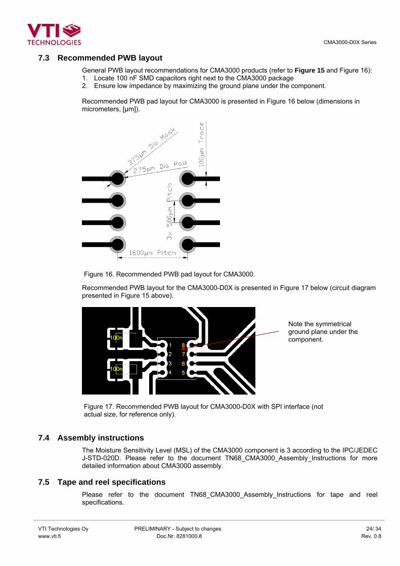
7.3 Recommended PWB layout General PWB layout recommendations for CMA3000 products (refer to Figure 15 and Figure 16): 1. Locate 100 nF SMD capacitors right next to the CMA3000 package 2. Ensure low impedance by maximizing the ground plane under the component. Recommended PWB pad layout for CMA3000 is presented in Figure 16 below (dimensions in micrometers, [µm]).
7.4 Assem
7.5 Tape a
Figure 16. Recommended PWB pad layout for CMA3000.
Oy PRELIMINARY - Subject to changes 24/ 34 Doc.Nr. 8281000.8 Rev. 0.8
Recommended PWB layout for the CMA3000-D0X is presented in Figure 17 below (circuit diagram presented in Figure 15 above).
Note the symmetrical ground plane under the component.
Figure 17. Recommended PWB layout for CMA3000-D0X with SPI interface (not actual size, for reference only).
bly instructions The Moisture Sensitivity Level (MSL) of the CMA3000 component is 3 according to the IPC/JEDEC J-STD-020D. Please refer to the document TN68_CMA3000_Assembly_Instructions for more detailed information about CMA3000 assembly. nd reel specifications Please refer to the document TN68_CMA3000_Assembly_Instructions for tape and reel specifications.

CMA3000-D0X Series
VTI Technologies www.vti.fi
8 Data sheet references 8.1 Offset
CMA3000's offset will be calibrated in X = 0 g, Y = 0 g, and Z = +1 g (Z measuring axis is parallel to earth’s gravitation) position, see Figure 18.
Y X
Z-axis in +1 g position
Earth’s gravitation
Pin #1
8.1.1 Offset
8.1.2 Offset
8.2 Sensit
Figure 18. CMA3000 offset (0 g) position.
Oy PRELIMINARY - Subject to changes 25/ 34 Doc.Nr. 8281000.8 Rev. 0.8
calibration error Offset calibration error is the difference between the sensor's actual output reading and the nominal output reading in calibration conditions. Error is calculated by
Equation 1
1000⋅−
= −− Sens
OutputOutputOffset axisXraxisCalibEX ,
where OutputX-axisCalibEr is sensor’s X-axis calibration error in [mg], OutputX-axis is sensor’s X-axis output reading [counts], Output is sensor’s nominal output in 0 g position and Sens sensor’s nominal sensitivity [counts/g]. temperature error Offset temperature error is the difference between the sensor's output reading in different temperatures and the sensor’s calibrated offset value at room temperature. Error is calculated by
Equation 2
1000@@@ ⋅
−= −−
− SensOutputOutput
Offset RTaxisXTaxisXTaxisTempErX ,
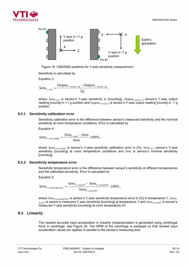
where OutputX-axisTempEr@T is sensor’s X-axis temperature error in [mg] in temperature T, OutputX-axis@T is sensor’s X-axis output reading [counts] in temperature T, OutputX-axis@T X-axis output reading [counts] at room temperature RT and Sens sensor’s nominal sensitivity [counts/g]. Sensor is in 0 g position for every measurement point. ivity During sensitivity calibration, the sensor is placed in ±1 g positions having one of the sensor’s measuring axis at a time parallel to the earth’s gravitation, see Figure 19.
CMA3000-D0X Series
VTI Technologies Owww.vti.fi
S
E
S
wrp
Pin #1
Z
Pin #1
X
Y-axis in -1 g position
Y-axis in +1 g position
X Z
Earth’s gravitation
8.2.1 SensitSs
E
S
ws[
8.2.2 SensitSa
E
S
wam
8.3 Lineari Tfa
Figure 19. CMA3000 positions for Y-axis sensitivity measurement.
y PRELIMINARY - Subject to changes 26/ 34 Doc.Nr. 8281000.8 Rev. 0.8
ensitivity is calculated by
quation 3
gOutputOutput
ens gaxisYgaxisYaxisY 2
1@1@ −−+−−
−= ,
here SensY-axis is sensor’s Y-axis sensitivity in [counts/g], OutputY-axis@+1g sensor’s Y-axis output eading [counts] in +1 g position and OutputY-axis@-1g is sensor’s Y-axis output reading [counts] in -1 g osition.
ivity calibration error ensitivity calibration error is the difference between sensor’s measured sensitivity and the nominal ensitivity at room temperature conditions. Error is calculated by
quation 4
%100⋅−
= −− Sens
SensSensens axisYraxisCalibEY ,
here SensY-axisCalibEr is sensor’s Y-axis sensitivity calibration error in [%], SensY-axis sensor’s Y-axis ensitivity [counts/g] at room temperature conditions and Sens is sensor’s nominal sensitivity counts/g].
ivity temperature error ensitivity temperature error is the difference between sensor’s sensitivity at different temperatures nd the calibrated sensitivity. Error is calculated by
quation 5
%100@
@@@ ⋅
−=
−
−−−
RTaxisY
RTaxisYTaxisYTaxisTempErY Sens
SensSensens ,
here SensY-axisTempEr@T is sensor’s Y-axis sensitivity temperature error in [%] in temperature T, SensY-
xis@T is sensor’s measured Y-axis sensitivity [counts/g] at temperature T and SensY-axis@RT is sensor’s easured Y-axis sensitivity [counts/g] at room temperature RT.
ty
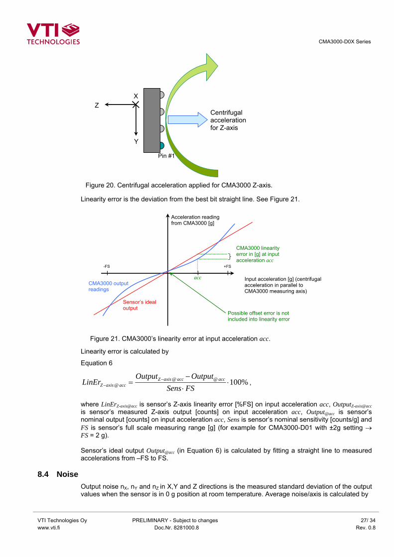
he needed accurate input acceleration in linearity characterization is generated using centrifugal orce in centrifuge, see Figure 20. The RPM of the centrifuge is sweeped so that wanted input cceleration values are applied in parallel to the sensor’s measuring axis.
CMA3000-D0X Series
VTI Technologies Oy PRELIMINARY - Subject to changes 27/ 34 www.vti.fi Doc.Nr. 8281000.8 Rev. 0.8
Linearity error is the deviation from the best bit straight line. See Figure 21. Linearity error is calculated by
Equation 6
%100@@@ ⋅
⋅−
= −− FSSens
OutputOutputLinEr accaccaxisZ
accaxisZ ,
where LinErZ-axis@acc is sensor’s Z-axis linearity error [%FS] on input acceleration acc, OutputZ-axis@acc is sensor’s measured Z-axis output [counts] on input acceleration acc, Output@acc is sensor’s nominal output [counts] on input acceleration acc, Sens is sensor’s nominal sensitivity [counts/g] and FS is sensor’s full scale measuring range [g] (for example for CMA3000-D01 with ±2g setting → FS = 2 g). Sensor’s ideal output Output@acc (in Equation 6) is calculated by fitting a straight line to measured accelerations from –FS to FS.
Pin #1
Centrifugal acceleration for Z-axis
X Z
Y
Figure 20. Centrifugal acceleration applied for CMA3000 Z-axis.
Input acceleration [g] (centrifugal acceleration in parallel to CMA3000 measuring axis)
CMA3000 linearity error in [g] at input acceleration acc
+FS-FS
Acceleration reading from CMA3000 [g]
acc
Sensor’s ideal output
CMA3000 output readings
Possible offset error is not included into linearity error
Figure 21. CMA3000’s linearity error at input acceleration acc.
8.4 Noise Output noise nX, nY and nZ in X,Y and Z directions is the measured standard deviation of the output values when the sensor is in 0 g position at room temperature. Average noise/axis is calculated by
CMA3000-D0X Series
VTI Technologies Oy PRELIMINARY - Subject to changes 28/ 34 www.vti.fi Doc.Nr. 8281000.8 Rev. 0.8
Equation 7
( )222
31
ZYX nnnn ++= ,
where n is sensor’s noise [g] per axis, nX is sensor’s X-axis noise [g], nY is sensor’s Y-axis noise [g] and nZ is sensor’s Z-axis noise [g]. CMA3000 demo-kit design can be used as a reference design for noise measurements, refer to “CMA3000 DEMO KIT User Manual TBD”.
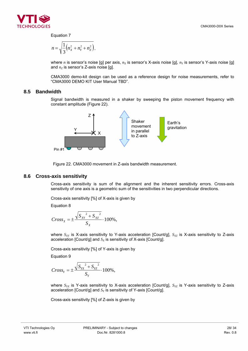
8.5 Bandwidth Signal bandwidth is measured in a shaker by sweeping the piston movement frequency with constant amplitude (Figure 22).
Z
YEarth’s gravitation
Shaker movement in parallel to Z-axis X
Pin #1
Figure 22. CMA3000 movement in Z-axis bandwidth measurement.
8.6 Cross-axis sensitivity Cross-axis sensitivity is sum of the alignment and the inherent sensitivity errors. Cross-axis sensitivity of one axis is a geometric sum of the sensitivities in two perpendicular directions. Cross-axis sensitivity [%] of X-axis is given by
Equation 8
%,10022
⋅+
±=X
XZXYX S
SSCross
where SXY is X-axis sensitivity to Y-axis acceleration [Count/g], SXZ is X-axis sensitivity to Z-axis acceleration [Count/g] and SX is sensitivity of X-axis [Count/g]. Cross-axis sensitivity [%] of Y-axis is given by
Equation 9
%,10022
⋅+
±=Y
YZYXY S
SSCross
where SYX is Y-axis sensitivity to X-axis acceleration [Count/g], SYZ is Y-axis sensitivity to Z-axis acceleration [Count/g] and SY is sensitivity of Y-axis [Count/g]. Cross-axis sensitivity [%] of Z-axis is given by
CMA3000-D0X Series
VTI Technologies Oy PRELIMINARY - Subject to changes 29/ 34 www.vti.fi Doc.Nr. 8281000.8 Rev. 0.8
Equation 10
%,10022
⋅+
±=Z
ZYZXZ S
SSCross
where SZX is Z-axis sensitivity to X-axis acceleration [Count/g], SZY is Z-axis sensitivity to Y-axis acceleration [Count/g] and SZ is sensitivity of Z-axis [Count/g]. Cross-axis sensitivity of CMA3000 family is measured in centrifuge over specified measurement range during qualification. Correct mounting position of component is important during the measurement of cross-axis sensitivity.
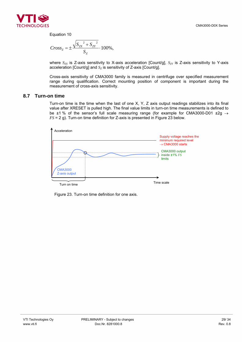
8.7 Turn-on time Turn-on time is the time when the last of one X, Y, Z axis output readings stabilizes into its final value after XRESET is pulled high. The final value limits in turn-on time measurements is defined to be ±1 % of the sensor’s full scale measuring range (for example for CMA3000-D01 ±2g → FS = 2 g). Turn-on time definition for Z-axis is presented in Figure 23 below.
CMA3000 output inside ±1% FS limits
CMA3000 Z-axis output
Acceleration
Turn on time Time scale
Supply voltage reaches thminimum required level → CMA3000 starts
e
Figure 23. Turn-on time definition for one axis.
CMA3000-D0X Series
VTI Technologies Oy PRELIMINARY - Subject to changes 30/ 34 www.vti.fi Doc.Nr. 8281000.8 Rev. 0.8
9 Known issues
9.1 Acceleration data reading via I2C bus CMA3000-D01 has a design issue (to be corrected) related to acceleration data reading via I2C bus: acceleration data reading during the INT-pin assertion (i.e. internal output register update) causes the data corruption. The following sections discuss how to overcome this.
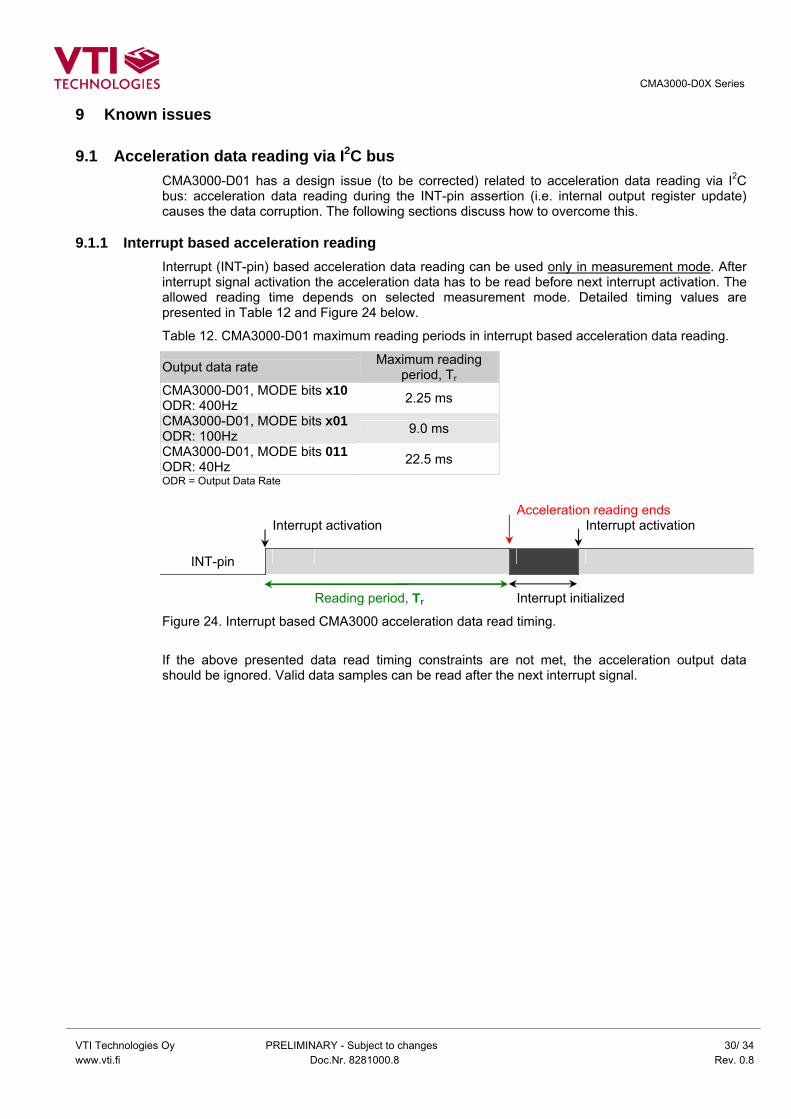
9.1.1 Interrupt based acceleration reading Interrupt (INT-pin) based acceleration data reading can be used only in measurement mode. After interrupt signal activation the acceleration data has to be read before next interrupt activation. The allowed reading time depends on selected measurement mode. Detailed timing values are presented in Table 12 and Figure 24 below.
Table 12. CMA3000-D01 maximum reading periods in interrupt based acceleration data reading.
Output data rate Maximum reading period, Tr
CMA3000-D01, MODE bits x10 ODR: 400Hz 2.25 ms
CMA3000-D01, MODE bits x01 ODR: 100Hz 9.0 ms
CMA3000-D01, MODE bits 011 ODR: 40Hz 22.5 ms ODR = Output Data Rate Acceleration reading ends Interrupt activation Interrupt activation
INT-pin
Reading period, Tr Interrupt initialized
Figure 24. Interrupt based CMA3000 acceleration data read timing.
If the above presented data read timing constraints are not met, the acceleration output data should be ignored. Valid data samples can be read after the next interrupt signal.

CMA3000-D0X Series
VTI Technologies Oy PRELIMINARY - Subject to changes 31/ 34 www.vti.fi Doc.Nr. 8281000.8 Rev. 0.8
9.1.2 Acceleration reading without interrupts
Acceleration data reading without interrupts can be used in all operation modes. Acceleration data is read out faster than CMA3000 can updates the acceleration output registers. When two identical XYZ acceleration values are received, the data is considered valid. The maximum data reading periods in different operation modes are presented below in Table 13.
Table 13. CMA3000-D01 maximum reading periods when interrupts are not detected.
Output data rate Maximum reading periodfor 3 samples, Tr
CMA3000-D01, MODE bits x10 ODR: 400Hz 2.4 ms
CMA3000-D01, MODE bits x01 ODR: 100Hz 9.9 ms
CMA3000-D01, MODE bits 011 ODR: 40Hz 24.0 ms
CMA3000-D01, MODE bits 100 ODR: 10Hz 90.0 ms ODR = Output Data Rate Internal acceleration
register update These two acceleration readings result identical
acceleration values → This result is accepted Internal acceleration
register update
Acceleration reading
→ corrupted Acceleration reading
Acceleration reading
Acceleration reading
→ corrupted
Acceleration data reading period for 3 samples, Tr
Figure 25. Interrupt based CMA3000 acceleration data read timing.
9.2 Leakage current when VDD - DVIO > 0.3 V
Due to design issue (to be corrected) a switch will leak some current, if the VDD will be approx 300 mV higher than DVIO. Typical leakage currents are according to the Table 14 below.
Table 14 CMA3000-D0X typical DVIO leakage current when VDD-DVIO>0.3V.
VDD/DVIO [V] Leakage current [µA] 2.5 / 1.7 25 3.6 / 1.7 100
9.3 Sensing element's bandwidth is lower than the target Due to design issue (to be corrected) sensing element's mechanical bandwidth is lower than the target. As a result, with 400 Hz output sample rate the bandwidth to X and Z direction is typically 60 Hz and to Y direction typically 90 Hz.
CMA3000-D0X Series
VTI Technologies Oy PRELIMINARY - Subject to changes 32/ 34 www.vti.fi Doc.Nr. 8281000.8 Rev. 0.8
10 Order Information Order code Description Packing Quantity CMA3000-D01-1 3-Axis accelerometer with SPI&I2C interface, +/- 2/8g, 100 pcs T&R 100 CMA3000-D01-10 3-Axis accelerometer with SPI&I2C interface, +/- 2/8g, 1000 pcs T&R 1000 CMA3000-D01-30 3-Axis accelerometer with SPI&I2C interface, +/- 2/8g, 3000 pcs T&R 3000 CMA3000-D01 PWB PWB assy 3-Axis accelerometer with SPI&I2C interface, +/- 2/8g Bulk 1 CMA3000-D01DEMO CMA3000-D01 DEMOKIT Bulk 1
CMA3000-D0X Series
VTI Technologies Oy PRELIMINARY - Subject to changes 33/ 34 www.vti.fi Doc.Nr. 8281000.8 Rev. 0.8
11 Document Change Control Version Date Change Description 0.1 06-Sep-07 Initial draft. 0.2 11-Jan-08 Major update. 0.3 14-Feb-08 Minor updates, corrections 0.4 18-Apr-08 Minor updates, section 'Known issues' added 0.5 01-Jul-08 Figure 1,&12 updated, table 9 updated 0.6 29-Aug-08 Sensitivities from 1/60 and 1/15 counts/g updated to 1/56 and 1/14 counts/g 0.7 10-Dec-08 Figure 12 updated. Tables 4, 5, 7, 9, 10 updated. Sections 9.2 and 9.3 added. 0.8 29-Dec-08 Launch version. Table 6 updated.
CMA3000-D0X Series
VTI Technologies Oy PRELIMINARY - Subject to changes 34/ 34 www.vti.fi Doc.Nr. 8281000.8 Rev. 0.8
12 Contact Information
Finland (head office) VTI Technologies Oy P.O. Box 27 Myllynkivenkuja 6 FI-01621 Vantaa Finland Tel. +358 9 879 181 Fax +358 9 8791 8791 E-mail: [email protected]
Germany VTI Technologies Oy Branch Office Frankfurt Rennbahnstrasse 72-74 D-60528 Frankfurt am Main, Germany Tel. +49 69 6786 880 Fax +49 69 6786 8829 E-mail: [email protected]
USA VTI Technologies, Inc. One Park Lane Blvd. Suite 804 - East Tower Dearborn, MI 48126 USA Tel. +1 313 425 0850 Fax +1 313 425 0860 E-mail: [email protected]
Japan VTI Technologies Oy Tokyo Office Tokyo-to, Minato-ku 2-7-16 Bureau Toranomon 401 105-0001 Japan Tel. +81 3 6277 6618 Fax +81 3 6277 6619 E-mail: [email protected]
China VTI Technologies Shanghai Office 6th floor, Room 618 780 Cailun Lu Pudong New Area 201203 Shanghai P.R. China Tel. +86 21 5132 0417 Fax +86 21 513 20 416 E-mail: [email protected]
To find out your local sales representative visit www.vti.fi

![VTI Glove Boxvti-glovebox.co.kr/vti-glovebox_kor_manual.pdf · 2016-03-12 · VTI Glove Box [Super] 사용자 1 1.VTI글로브박스소개 본사용자설명서의VTI글로브박스는최신기술이사용되어설계되고만들어졌습니다](https://img.pdfslide.net/doc/110x75/5f0ba21e7e708231d43176e4/vti-glove-boxvti-2016-03-12-vti-glove-box-super-1-1vtieeoeeoeeoeeoe.jpg)