Embed Size (px)
Citation preview
Programmable Phase/Frequency Generatorfor System Debug and Diagnosis
Tsung-Yen Tsai
Department of Electrical & Computer EngineeringMcGill UniversityMontreal, Canada
July 2011
A thesis submitted to McGill University in partial fulfillment of the requirements for thedegree of Master of Engineering.
c© 2011 Tsung-Yen Tsai
i
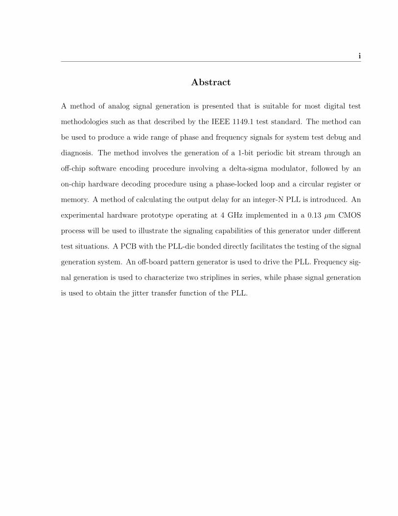
Abstract
A method of analog signal generation is presented that is suitable for most digital test
methodologies such as that described by the IEEE 1149.1 test standard. The method can
be used to produce a wide range of phase and frequency signals for system test debug and
diagnosis. The method involves the generation of a 1-bit periodic bit stream through an
off-chip software encoding procedure involving a delta-sigma modulator, followed by an
on-chip hardware decoding procedure using a phase-locked loop and a circular register or
memory. A method of calculating the output delay for an integer-N PLL is introduced. An
experimental hardware prototype operating at 4 GHz implemented in a 0.13 µm CMOS
process will be used to illustrate the signaling capabilities of this generator under different
test situations. A PCB with the PLL-die bonded directly facilitates the testing of the signal
generation system. An off-board pattern generator is used to drive the PLL. Frequency sig-
nal generation is used to characterize two striplines in series, while phase signal generation
is used to obtain the jitter transfer function of the PLL.
ii
Abrege
Une methode de generation de signaux analogiques qui est appropriee pour la plupart des
methodes de test digitale comme decrit par le standard de test IEEE 1149.1 est presentee.
Cette methode peut etre utilisee pour produire une serie de signaux encodes dans la phase
et la frequence des fins de tests tel que «system test debug» et «system test diagnosis».
La methode consiste a produire un signal periodique digitale consistant d’une seule valeur
binaire a l’aide d’un module «software» externe au circuit integre et de le decoder dans le
circuit integre a l’aide d’un PLL et une memoire ou bien un registre circulaire. Le module
«software» externe au circuit integre consiste d’un modulateur delta-sigma. Par la suite,
une methode pour calculer le delais du «output» d’un «integer-N PLL» est presentee. Un
prototype experimentale sur circuit integre CMOS 0.13 µm est utilise pour demontrer la
viabilite de cette methode a une frequence de 4 GHz. Finalement pour tester le prototype
experimental sur circuit integre en CMOS 0.13 µm, un PCB a ete concu pour que l’on
puisse y attache le circuit integre avec du «bond wiring». Pour le test, un generateur de
signaux externes fut utilise pour modeliser deux «striplines» en serie pendant qu’un signal
encode dans la phase fut utilise pour deduire le «jitter transfer function» du PLL.
iii
Acknowledgments
I would like to thank my supervisor, Gordon W. Roberts, for without his patience and
guidance this thesis would not have been possible. Thanks also goes to Sadok Aouini
for his help in getting me up and running in Simulink simulations, to the guys on the
same tapeout (Ali Ameri, George Gal, Marco Macedo) for all the help with those strange
DRC and LVS errors, Azhar Chowdhury for the assistance with phase measurements, and
everyone in the lab for just being there and for everything I’m sure I’ve forgotten.
Thanks goes to especially my parents, without whose continuing support I am sure I
would not be writing this.
iv
Contents
1 Introduction 1
1.1 Basic Principles of the IEEE 1149.1 Test Bus . . . . . . . . . . . . . . . . . 2
1.2 State-of-the-Art High-Speed Signal Generation . . . . . . . . . . . . . . . . . 4
1.3 Thesis Outline . . . . . . . . . . . . . . . . . . . . . . . . . . . . . . . . . . . 6
2 Phase/Frequency Synthesis 7
2.1 Delta-Sigma-based Phase/Frequency Generation . . . . . . . . . . . . . . . . 7
2.2 Building Blocks . . . . . . . . . . . . . . . . . . . . . . . . . . . . . . . . . . 8
2.2.1 Software-Based Delta-Sigma Modulator . . . . . . . . . . . . . . . . . 8
2.2.2 Digital-to-Frequency Conversion . . . . . . . . . . . . . . . . . . . . . 9
2.2.3 Digital-to-Time (Phase) Conversion . . . . . . . . . . . . . . . . . . . 10
2.2.4 Phase-Locked Loop/Anti-Imaging Filter . . . . . . . . . . . . . . . . 12
2.2.5 Overall Phase/Frequency System Behaviour . . . . . . . . . . . . . . 14
2.3 Verification of Phase/Frequency System Behaviour . . . . . . . . . . . . . . 15
2.3.1 Software-Based Delta-Sigma Modulator . . . . . . . . . . . . . . . . . 15
2.3.2 DFC/DTC . . . . . . . . . . . . . . . . . . . . . . . . . . . . . . . . 18
2.3.3 PLL . . . . . . . . . . . . . . . . . . . . . . . . . . . . . . . . . . . . 18
2.3.4 Frequency/Phase System Simulation . . . . . . . . . . . . . . . . . . 25
Contents v
2.4 Summary . . . . . . . . . . . . . . . . . . . . . . . . . . . . . . . . . . . . . 28
3 PLL Design 29
3.1 Transistor-Level Design . . . . . . . . . . . . . . . . . . . . . . . . . . . . . . 29
3.1.1 Phase-Frequency Detector . . . . . . . . . . . . . . . . . . . . . . . . 30
3.1.2 Charge Pump . . . . . . . . . . . . . . . . . . . . . . . . . . . . . . . 31
3.1.3 Voltage-Controlled Oscillator . . . . . . . . . . . . . . . . . . . . . . 34
3.1.4 Frequency Divider . . . . . . . . . . . . . . . . . . . . . . . . . . . . 36
3.1.5 Loop Filter . . . . . . . . . . . . . . . . . . . . . . . . . . . . . . . . 37
3.1.6 Input/Output Circuitry . . . . . . . . . . . . . . . . . . . . . . . . . 40
3.2 Layout . . . . . . . . . . . . . . . . . . . . . . . . . . . . . . . . . . . . . . . 43
3.3 Transistor-Level Simulations . . . . . . . . . . . . . . . . . . . . . . . . . . . 45
3.3.1 Phase-Frequency Detector . . . . . . . . . . . . . . . . . . . . . . . . 45
3.3.2 Charge Pump . . . . . . . . . . . . . . . . . . . . . . . . . . . . . . . 47
3.3.3 Loop Filter . . . . . . . . . . . . . . . . . . . . . . . . . . . . . . . . 48
3.3.4 Frequency Dividers . . . . . . . . . . . . . . . . . . . . . . . . . . . . 49
3.3.5 Voltage-Controlled Oscillator . . . . . . . . . . . . . . . . . . . . . . 51
3.3.6 Input/Output Circuitry . . . . . . . . . . . . . . . . . . . . . . . . . 55
3.3.7 PLL . . . . . . . . . . . . . . . . . . . . . . . . . . . . . . . . . . . . 57
3.4 Summary . . . . . . . . . . . . . . . . . . . . . . . . . . . . . . . . . . . . . 58
4 PCB Design 59
4.1 Filter Test PCB . . . . . . . . . . . . . . . . . . . . . . . . . . . . . . . . . . 59
4.2 Chip-Bonded PCB . . . . . . . . . . . . . . . . . . . . . . . . . . . . . . . . 62
4.2.1 Grounding and Stackup . . . . . . . . . . . . . . . . . . . . . . . . . 62
4.2.2 Decoupling . . . . . . . . . . . . . . . . . . . . . . . . . . . . . . . . 64
Contents vi
4.2.3 Input/Output . . . . . . . . . . . . . . . . . . . . . . . . . . . . . . . 65
4.2.4 Component Selection . . . . . . . . . . . . . . . . . . . . . . . . . . . 67
4.2.5 Die Bonding . . . . . . . . . . . . . . . . . . . . . . . . . . . . . . . . 69
4.2.6 Fabrication . . . . . . . . . . . . . . . . . . . . . . . . . . . . . . . . 70
4.3 Summary . . . . . . . . . . . . . . . . . . . . . . . . . . . . . . . . . . . . . 73
5 Experimental Results 74
5.1 Test Setup . . . . . . . . . . . . . . . . . . . . . . . . . . . . . . . . . . . . . 74
5.2 Clock Input . . . . . . . . . . . . . . . . . . . . . . . . . . . . . . . . . . . . 79
5.3 Frequency Signal Generation . . . . . . . . . . . . . . . . . . . . . . . . . . . 81
5.4 Phase Signal Generation . . . . . . . . . . . . . . . . . . . . . . . . . . . . . 85
5.5 Summary . . . . . . . . . . . . . . . . . . . . . . . . . . . . . . . . . . . . . 88
6 Conclusions 89
6.1 Thesis Contributions . . . . . . . . . . . . . . . . . . . . . . . . . . . . . . . 89
6.2 Future Work . . . . . . . . . . . . . . . . . . . . . . . . . . . . . . . . . . . . 90
A Perl Script for Pattern Generator 91
References 93
vii
List of Figures
1.1 System implementation of on-chip high-frequency generator utilizing the
1149.1 test bus standard. . . . . . . . . . . . . . . . . . . . . . . . . . . . . 2
1.2 IEEE 1149.1 test bus block diagram. . . . . . . . . . . . . . . . . . . . . . . 3
1.3 Voltage mode signal generation block diagram. . . . . . . . . . . . . . . . . 6
2.1 Phase/Frequency synthesis block diagram. . . . . . . . . . . . . . . . . . . . 8
2.2 First order delta-sigma modulator with STF = 1. . . . . . . . . . . . . . . . 9
2.3 Block diagram representation of digital-to-frequency mapping. . . . . . . . . 11
2.4 Block diagram representation of digital-to-time mapping. . . . . . . . . . . 12
2.5 PLL block diagram with design variables. . . . . . . . . . . . . . . . . . . . 13
2.6 Delta-sigma Simulink state-space model. . . . . . . . . . . . . . . . . . . . . 17
2.7 Output PSD of delta-sigma modulator with 0.434 DC input. . . . . . . . . 17
2.8 Output of DFC in time domain with 0.434 DC input. . . . . . . . . . . . . 18
2.9 Output of DTC in time domain with 0.434 DC input. . . . . . . . . . . . . 19
2.10 PLL Simulink model with frequency measurement subsystem. . . . . . . . . 21
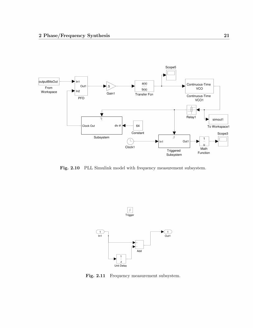
2.11 Frequency measurement subsystem. . . . . . . . . . . . . . . . . . . . . . . 21
2.12 Frequency division subsystem. . . . . . . . . . . . . . . . . . . . . . . . . . 22
2.13 PLL Simulink model with phase measurement subsystem. . . . . . . . . . . 22
List of Figures viii
2.14 Phase measurement subsystem. . . . . . . . . . . . . . . . . . . . . . . . . . 23
2.15 PLL closed-loop transfer function. . . . . . . . . . . . . . . . . . . . . . . . 23
2.16 PLL loop filter transfer function. . . . . . . . . . . . . . . . . . . . . . . . . 24
2.17 Three tones produced by the frequency generator. . . . . . . . . . . . . . . 26
2.18 Output spectrum of 0.01 amp., 2 MHz phase-encoded signal with 4.16 GHz
carrier. . . . . . . . . . . . . . . . . . . . . . . . . . . . . . . . . . . . . . . 27
2.19 Simulated output phase vs. DC code. . . . . . . . . . . . . . . . . . . . . . 27
3.1 General block diagram of charge pump PLL. . . . . . . . . . . . . . . . . . 30
3.2 Block diagram of PFD. . . . . . . . . . . . . . . . . . . . . . . . . . . . . . 31
3.3 Schematic of modified TSPC D flip-flop. [19] . . . . . . . . . . . . . . . . . 32
3.4 Schematic of charge pump. [23] . . . . . . . . . . . . . . . . . . . . . . . . . 33
3.5 Multiple-pass VCO block diagram. [24] . . . . . . . . . . . . . . . . . . . . 35
3.6 Schematic of VCO delay cell. [24] . . . . . . . . . . . . . . . . . . . . . . . . 35
3.7 Block diagram of frequency divider. [25] . . . . . . . . . . . . . . . . . . . . 36
3.8 Schematic of CML frequency divider. [26] . . . . . . . . . . . . . . . . . . . 37
3.9 Schematic of TSPC latch. [20] . . . . . . . . . . . . . . . . . . . . . . . . . 38
3.10 Loop filter schematic. [27], [16] . . . . . . . . . . . . . . . . . . . . . . . . . 40
3.11 Input buffer schematic. [28] . . . . . . . . . . . . . . . . . . . . . . . . . . . 41
3.12 CML buffer schematic. [30] . . . . . . . . . . . . . . . . . . . . . . . . . . . 42
3.13 PLL chip layout. . . . . . . . . . . . . . . . . . . . . . . . . . . . . . . . . . 43
3.14 Close-up of PLL layout with annotated components. . . . . . . . . . . . . . 44
3.15 Implementation specific block diagram of PLL. . . . . . . . . . . . . . . . . 45
3.16 Transient simulation of PFD. . . . . . . . . . . . . . . . . . . . . . . . . . . 46
3.17 Transient simulation of charge pump. . . . . . . . . . . . . . . . . . . . . . 47
List of Figures ix
3.18 AC analysis of loop filter. . . . . . . . . . . . . . . . . . . . . . . . . . . . . 48
3.19 Transient simulation of TSPC dividers. . . . . . . . . . . . . . . . . . . . . 49
3.20 Transient simulation of CML divider. . . . . . . . . . . . . . . . . . . . . . 50
3.21 Transient simulation of VCO. . . . . . . . . . . . . . . . . . . . . . . . . . . 52
3.22 VCO output frequency versus input voltage. . . . . . . . . . . . . . . . . . 53
3.23 PNOISE simulation of VCO. . . . . . . . . . . . . . . . . . . . . . . . . . . 54
3.24 Transient simulation of CMOS input level shifter. . . . . . . . . . . . . . . . 55
3.25 Transient simulation of CML output buffer. . . . . . . . . . . . . . . . . . . 56
3.26 Transient simulation of PLL control voltage. . . . . . . . . . . . . . . . . . 57
4.1 Filter test PCB with 30 AWG wires for debugging. . . . . . . . . . . . . . . 61
4.2 PLL PCB ground plane. . . . . . . . . . . . . . . . . . . . . . . . . . . . . . 63
4.3 PLL PCB stackup. . . . . . . . . . . . . . . . . . . . . . . . . . . . . . . . . 64
4.4 AC simulation of decoupling network. . . . . . . . . . . . . . . . . . . . . . 66
4.5 Microstrip test coupon. . . . . . . . . . . . . . . . . . . . . . . . . . . . . . 68
4.6 Front of PCB with PLL die marked using white square at centre of diagram. 71
4.7 Back of PCB. . . . . . . . . . . . . . . . . . . . . . . . . . . . . . . . . . . . 72
5.1 Phase/frequency generation system test setup. . . . . . . . . . . . . . . . . 75
5.2 PLL die micrograph. . . . . . . . . . . . . . . . . . . . . . . . . . . . . . . . 76
5.3 Measurement equipment stack. . . . . . . . . . . . . . . . . . . . . . . . . . 77
5.4 Power supplies and PCB under measurement. . . . . . . . . . . . . . . . . . 78
5.5 PSD of PLL output with 67 MHz clock input. . . . . . . . . . . . . . . . . 80
5.6 Cycle-to-cycle jitter of PLL output for 65 MHz clock input. . . . . . . . . . 80
5.7 Measured spectrum of PLL output for 0.434V DC input. . . . . . . . . . . . 82
5.8 Time domain capture of PLL output for 0.434V DC input. . . . . . . . . . 83
List of Figures x
5.9 Output voltage vs. freq. over 500 MHz range centred at 4.2 GHz. . . . . . . 83
5.10 Comparison of stripline characterization with frequency signal generator and
external synthesizer. . . . . . . . . . . . . . . . . . . . . . . . . . . . . . . . 84
5.11 Time domain PLL output with respect to reference clock, 0.434V DC input. 86
5.12 Measured and simulated output phase vs. DC code. . . . . . . . . . . . . . 87
5.13 Measured PLL jitter transfer function vs. ideal at 4.16 GHz. . . . . . . . . 87
xi
List of Tables
2.1 Digital-To-Frequency Mapping . . . . . . . . . . . . . . . . . . . . . . . . . . 10
2.2 Digital-To-Time Mapping . . . . . . . . . . . . . . . . . . . . . . . . . . . . 12
3.1 PFD D Flip-Flop Transistor Sizing . . . . . . . . . . . . . . . . . . . . . . . 31
3.2 Charge Pump Transistor Sizing . . . . . . . . . . . . . . . . . . . . . . . . . 33
3.3 VCO Transistor Sizing . . . . . . . . . . . . . . . . . . . . . . . . . . . . . . 34
3.4 CML Divider Sizing . . . . . . . . . . . . . . . . . . . . . . . . . . . . . . . . 37
3.5 TSPC Latch Sizing . . . . . . . . . . . . . . . . . . . . . . . . . . . . . . . . 38
3.6 Loop Filter Component Values . . . . . . . . . . . . . . . . . . . . . . . . . . 40
3.7 Input Buffer Sizing . . . . . . . . . . . . . . . . . . . . . . . . . . . . . . . . 41
3.8 CML Buffer Transistor Sizing . . . . . . . . . . . . . . . . . . . . . . . . . . 42
3.9 CML Buffer Resistor Values . . . . . . . . . . . . . . . . . . . . . . . . . . . 43
4.1 PCB Manufacturing Costs . . . . . . . . . . . . . . . . . . . . . . . . . . . . 73
5.1 Clock Measurement Results . . . . . . . . . . . . . . . . . . . . . . . . . . . 81
5.2 Frequencies Generated . . . . . . . . . . . . . . . . . . . . . . . . . . . . . . 82
5.3 Phase Output Results . . . . . . . . . . . . . . . . . . . . . . . . . . . . . . 86
1
Chapter 1
Introduction
The ability to generate high-frequency test signals on-chip that can be made to vary over
frequency and phase under external program control provides a useful debug and diagnosis
tool. As operating frequencies and pin counts rise, it is increasingly difficult and costly
to route high-speed signals on and off-chip. Many factors need to be considered, such as
impedance matching, mismatch uncertainty, crosstalk, and clock skew among others, re-
quiring extensive analysis. Also, adding pins in an already crowded package exclusively for
testing may not be acceptable in all situations. As such, design-for-test (DFT) techniques
that make use of facilities that already exist on-chip are desirable. In the approach suggested
here, most if not all components would already exist on chip. Specifically, the technique
requires the use of a circular digital register (referred to as the delta-sigma register) for
repeating a specific digital pattern and a phase-lock loop (PLL) to remove out-of-band
quantization noise as depicted in Figure 1.1. Communications on and off-chip would gener-
ally be accomplished using the test ports associated with the test bus standard (e.g., TDI
and TDO). In this thesis, we limit our discussion to the generation of high-frequency signals
on-chip under external program control. Signal capture and transporting results are not
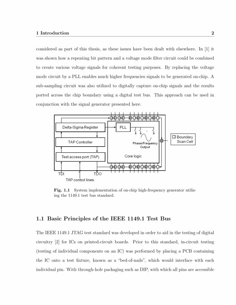
1 Introduction 2
considered as part of this thesis, as these issues have been dealt with elsewhere. In [1] it
was shown how a repeating bit pattern and a voltage mode filter circuit could be combined
to create various voltage signals for coherent testing purposes. By replacing the voltage
mode circuit by a PLL enables much higher frequencies signals to be generated on-chip. A
sub-sampling circuit was also utilized to digitally capture on-chip signals and the results
ported across the chip boundary using a digital test bus. This approach can be used in
conjunction with the signal generator presented here.
Fig. 1.1 System implementation of on-chip high-frequency generator utiliz-ing the 1149.1 test bus standard.
1.1 Basic Principles of the IEEE 1149.1 Test Bus
The IEEE 1149.1 JTAG test standard was developed in order to aid in the testing of digital
circuitry [2] for ICs on printed-circuit boards. Prior to this standard, in-circuit testing
(testing of individual components on an IC) was performed by placing a PCB containing
the IC onto a test fixture, known as a “bed-of-nails”, which would interface with each
individual pin. With through-hole packaging such as DIP, with which all pins are accessible
1 Introduction 3
in a row underneath the PCB, designing the fixture and test circuitry is relatively simple.
However, with the advent of SMT (surface mount technology) devices, the fine pitch and
density does not allow direct access to pins. Instead, vias and pads must be specially made
for test purposes, increasing test complexity. In addition, it is difficult to identify whether
a fault is with the IC itself or with the associated interconnect, making it possible that
perfectly good chips are being thrown away. The IEEE 1149.1 boundary scan architecture
is specifically designed to alleviate these issues. The serially connected boundary scan cells
allow each I/O to be tested through a serial bus, without requiring individual connections
to each pin or pad. There are specific provisions for testing interconnections between two
IEEE 1149.1-equipped chips. Also, many ICs on one PCB can be “daisy-chained”, further
reducing the number of testing-specific connections required for the entire system on the
same PCB.
Core Logic
Boundary
Scan Cell
Identification Register
Instruction Register
TAP
Controller
Bypass
Register
Boundary
Scan Cell
Boundary
Scan Cell
Boundary
Scan Cell
Boundary
Scan Cell
Boundary
Scan Cell
Boundary
Scan Cell
Boundary
Scan Cell
Boundary
Scan Cell
TDI
TMS
TCK
TDO
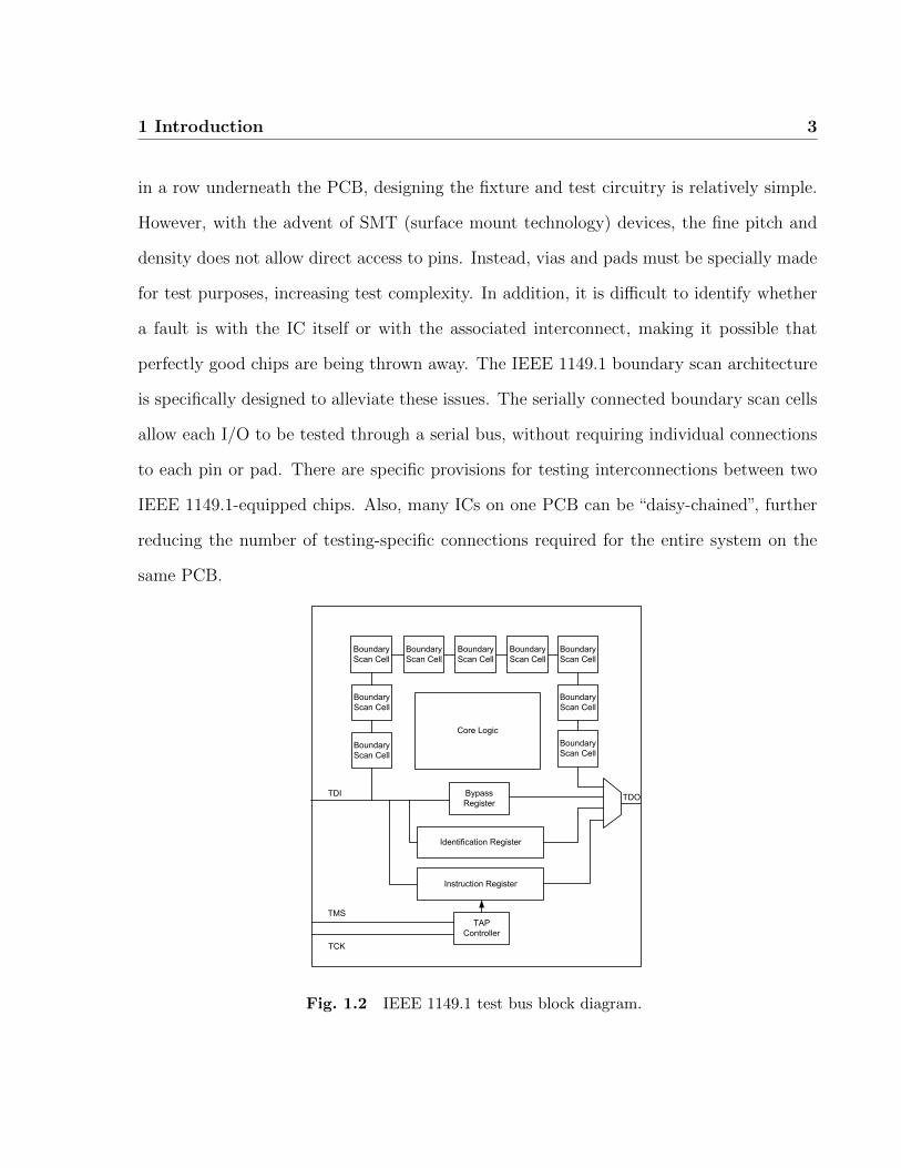
Fig. 1.2 IEEE 1149.1 test bus block diagram.
1 Introduction 4
The IEEE 1149.1 test bus consists of four test pins: TDI, TDO, TCK, TMS, and
optionally TRST. TDI and TDO are the test data in/out pins, respectively, while TCK is
the test clock, TMS is test mode select, and TRST is an optional asynchronous reset pin
[2]. These make up what is known as the Test Access Port, commonly referred to as the
TAP. A TAP controller decodes instructions regarding the configuration of the scan cells
and registers. Only one register or the scan chain is allowed to be connected at a time to
TDI/TDO. A block diagram is shown in Figure 1.2. The bypass register allows on-board
testing by passing instructions onto the next chip in the chain, while the identification
register contains a 32-bit identifying string. The instruction register stores the current
instruction. The standard specifies that aside from four mandatory instructions (Bypass,
Sample, Preload, and Extest) and other optional ones, the designer may implement private
instructions. Therefore, it should be possible to utilize the TAP controller to configure an
additional register (called the delta-sigma register in Figure 1.1) to use TDI to receive a
bitstream, then to cycle the bits to act as an uninterrupted bitstream for the proposed
signal generator.
1.2 State-of-the-Art High-Speed Signal Generation
In general, high speed frequency synthesizers implemented in CMOS processes tend to be
PLL-based [3] due to the their high performance and relatively compact size. A divider is
required to reach high frequencies, as it is unlikely a high quality reference exists in the
gigahertz operating region. For closely spaced frequencies in RF-type applications (such as
for a local oscillator feeding a RF mixer in a receiver), integer-N PLLs greatly restrict the
frequency of the input reference that can be used, since the input reference frequency must
be equal to the channel spacing. In [4], a 1.2 GHz delta-sigma fractional-N synthesizer was
1 Introduction 5
built in 0.18 µm CMOS with -121 dBc/Hz phase noise at 1 MHz offset. For applications
with wider channel spacing, integer-N PLLs are often used. In [5], [6] and [7], integer-N
synthesizers with -110 dBc/Hz phase noise @ 1 MHz offset from a 5 GHz carrier, -104.5
dBc/Hz @ 1 MHz offset from a 9 GHz carrier, and -104 dBc/Hz @ 1 MHz offset from a
5 GHz carrier, respectively, were built in CMOS technology. However, these synthesizers
all tend to occupy large die areas, ranging from 0.55 mm x 0.9 mm [5] to 1.31 mm x 1.26
mm [4]. Synthesizers with all-digital PLLs (ADPLL) have also been gaining popularity; an
example is [8], where a 10 GHz all-digital frequency synthesizer was built on 90 nm CMOS
with -100 dBc/Hz @ 1 MHz phase noise with 10 GHz carrier. The die size occupied is still
large, at 0.902 mm2. Traditional high-speed frequency synthesis techniques deliver high
performance, but may not be suitable for on-die testing applications1, as a large amount of
space may be required for the signal generation block alone.
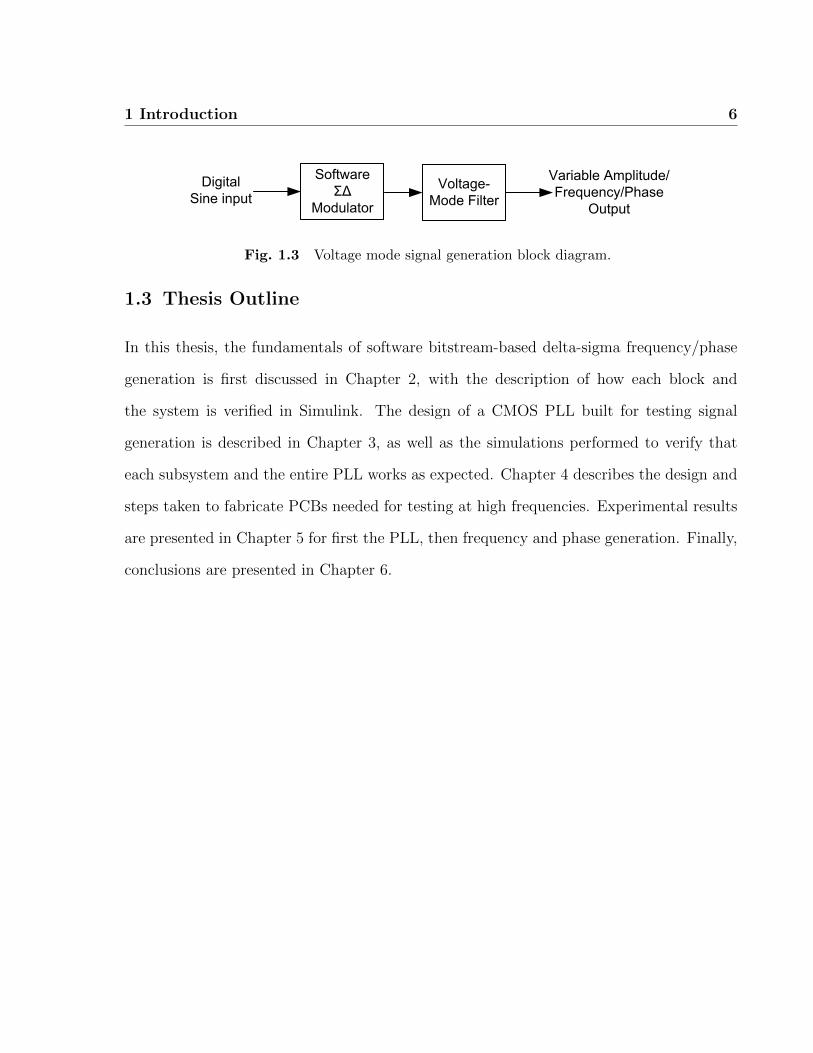
Previous work on software-based delta-sigma signal generation techniques has been in
the voltage domain. Generally, a digitally generated sine wave is input to a software-
based delta-sigma modulator, and a voltage-mode anti-imaging filter removes the shaped
quantization noise. A register containing the delta-sigma output bits is cycled to create an
uninterrupted bitstream. The block diagram of this system is shown in Figure 1.3. The
reconstruction filter may be low-pass or bandpass, depending on the type of delta-sigma
modulator used [9]. The output frequency of this type of signal generation is restricted to
the bandwidth of the modulator. For example, in [10], a 100 MHz signal was generated. By
using a PLL as a time-mode anti-imaging filter, much higher speeds can be achieved. This
is desirable as this signal can be used, for instance, to aid in the debug of high frequency
components on-chip.
1These applications include Built-In Self Test (BIST).
1 Introduction 6
Software
ΣΔ
Modulator
Voltage-
Mode Filter
Digital
Sine input
Variable Amplitude/
Frequency/Phase
Output
Fig. 1.3 Voltage mode signal generation block diagram.
1.3 Thesis Outline
In this thesis, the fundamentals of software bitstream-based delta-sigma frequency/phase
generation is first discussed in Chapter 2, with the description of how each block and
the system is verified in Simulink. The design of a CMOS PLL built for testing signal
generation is described in Chapter 3, as well as the simulations performed to verify that
each subsystem and the entire PLL works as expected. Chapter 4 describes the design and
steps taken to fabricate PCBs needed for testing at high frequencies. Experimental results
are presented in Chapter 5 for first the PLL, then frequency and phase generation. Finally,
conclusions are presented in Chapter 6.
7
Chapter 2
Phase/Frequency Synthesis
Phase/frequency synthesis serves to generate a signal of a specific frequency or phase. A
signal generation system using a software-based delta-sigma modulator, a digital-to-time
or digital-to-frequency converter, followed by a PLL is described. The system is verified in
Simulink, and the results compared with theoretical values.
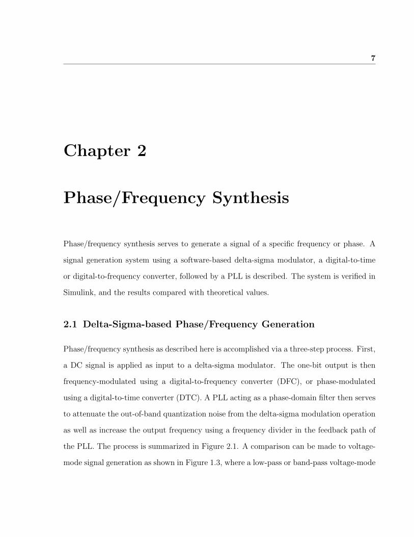
2.1 Delta-Sigma-based Phase/Frequency Generation
Phase/frequency synthesis as described here is accomplished via a three-step process. First,
a DC signal is applied as input to a delta-sigma modulator. The one-bit output is then
frequency-modulated using a digital-to-frequency converter (DFC), or phase-modulated
using a digital-to-time converter (DTC). A PLL acting as a phase-domain filter then serves
to attenuate the out-of-band quantization noise from the delta-sigma modulation operation
as well as increase the output frequency using a frequency divider in the feedback path of
the PLL. The process is summarized in Figure 2.1. A comparison can be made to voltage-
mode signal generation as shown in Figure 1.3, where a low-pass or band-pass voltage-mode
2 Phase/Frequency Synthesis 8
filter is used after the delta-sigma modulation. The former approach involving the PLL
enhances the frequency generation to the GHz regime.
Software
ΣΔ
Modulator
PLLDFC/DTCDigital
DC input
Variable
Frequency/
Phase Output
Fig. 2.1 Phase/Frequency synthesis block diagram.
2.2 Building Blocks
2.2.1 Software-Based Delta-Sigma Modulator
The delta-sigma modulator serves to convert a DC voltage into a one-bit digital signal (i.e.,
as an ADC) in this system. It also confers the added advantage of shaping the quantization
noise introduced by the conversion process to higher frequencies outside the band of interest,
which can be controlled by the sampling frequency fs of the modulator.
The structure of the delta-sigma modulator used is shown in Figure 2.2. Its signal
transfer function (STF) is unity, while its noise transfer function (NTF) is 1/(1+H(z)).
The STF affects the input signal; in this case, with STF equal to unity, the input signal
is not affected by the modulator. The NTF determines how the modulator shapes the
quantization noise, and also the modulator type (lowpass, bandpass, etc.) and order [11].
Only a lowpass type modulator is used in the system described. The NTF can be designed
as a filter, with a response that correspond to the requirements needed (e.g., Chebyshev,
Butterworth, elliptic-type responses). The DSMOD tool for Matlab is able to design the
NTF for a delta-sigma modulator once given parameters such as type and order [12]. The
modulator bandwidth is governed by the sampling frequency and the oversampling ratio
(OSR) used, as shown in Equation below.
2 Phase/Frequency Synthesis 9
BW =fs,∆Σ
2 ∗OSR(2.1)
The comparator shown in Figure 2.2 is used as a 1-bit quantizer, setting the output to a
logical “1” or “0” depending on the input signal as compared to a set threshold. The high
and low output levels of the quantizer (and the modulator) are referred to as ∆Σmax and
∆Σmin, respectively.
+
+
H(z)
x(n)
e(n)
y(n)
+ -
Fig. 2.2 First order delta-sigma modulator with STF = 1.
A popular performance metric for the delta-sigma modulator is its signal-to-noise ratio
(SNR). This is the ratio of signal power to noise power within the passband region of the
delta-sigma modulator. This metric is affected, among other factors, by the modulator
order, oversampling ratio, and NTF design factors such as pole and zero placement.
2.2.2 Digital-to-Frequency Conversion
A frequency modulation operation is performed on the output of the one-bit delta-sigma
modulator. This results in another one-bit stream appearing at its output that contains
an instantaneous frequency component that depends on the density of the ones and zeros
appearing at its input. To achieve a constant output frequency, a 1-bit input stream with
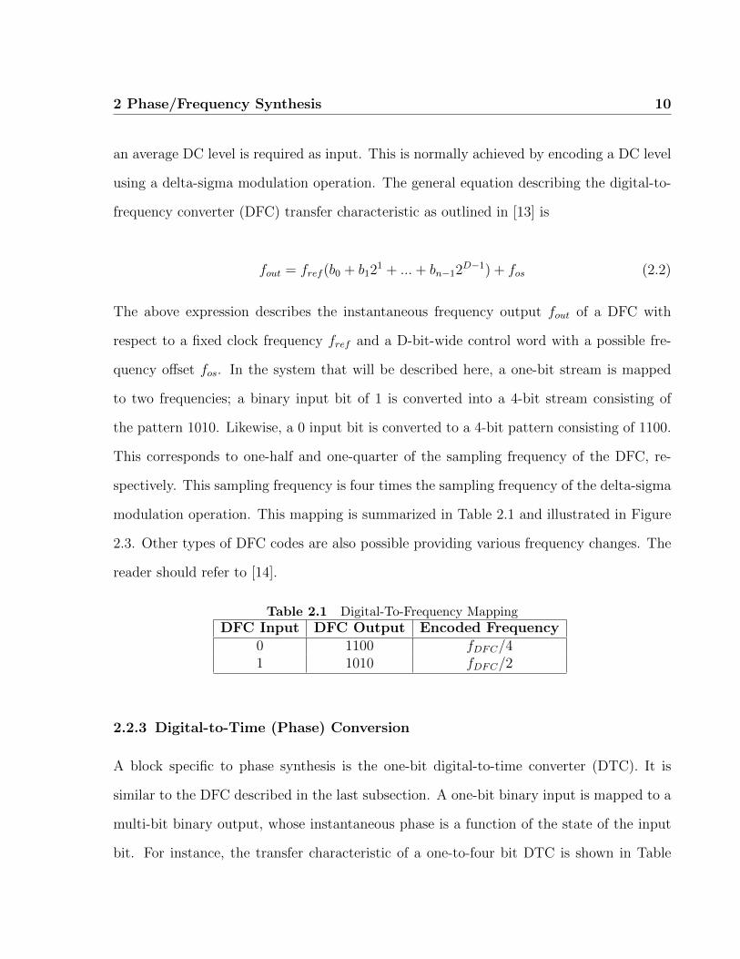
2 Phase/Frequency Synthesis 10
an average DC level is required as input. This is normally achieved by encoding a DC level
using a delta-sigma modulation operation. The general equation describing the digital-to-
frequency converter (DFC) transfer characteristic as outlined in [13] is
fout = fref (b0 + b121 + ...+ bn−12D−1) + fos (2.2)
The above expression describes the instantaneous frequency output fout of a DFC with
respect to a fixed clock frequency fref and a D-bit-wide control word with a possible fre-
quency offset fos. In the system that will be described here, a one-bit stream is mapped
to two frequencies; a binary input bit of 1 is converted into a 4-bit stream consisting of
the pattern 1010. Likewise, a 0 input bit is converted to a 4-bit pattern consisting of 1100.
This corresponds to one-half and one-quarter of the sampling frequency of the DFC, re-
spectively. This sampling frequency is four times the sampling frequency of the delta-sigma
modulation operation. This mapping is summarized in Table 2.1 and illustrated in Figure
2.3. Other types of DFC codes are also possible providing various frequency changes. The
reader should refer to [14].
Table 2.1 Digital-To-Frequency MappingDFC Input DFC Output Encoded Frequency
0 1100 fDFC/41 1010 fDFC/2
2.2.3 Digital-to-Time (Phase) Conversion
A block specific to phase synthesis is the one-bit digital-to-time converter (DTC). It is
similar to the DFC described in the last subsection. A one-bit binary input is mapped to a
multi-bit binary output, whose instantaneous phase is a function of the state of the input
bit. For instance, the transfer characteristic of a one-to-four bit DTC is shown in Table
2 Phase/Frequency Synthesis 11
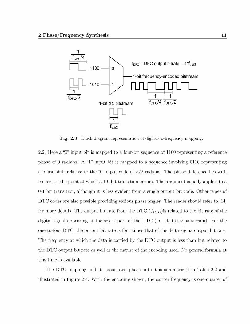
1100
1010 1
0
1-bit ΔΣ bitstream
1-bit frequency-encoded bitstream
fDFC = DFC output bitrate = 4*fs,ΔΣ
fs,ΔΣ
1
fDFC/21
fDFC/41
fDFC/41
fDFC/21
Fig. 2.3 Block diagram representation of digital-to-frequency mapping.
2.2. Here a “0” input bit is mapped to a four-bit sequence of 1100 representing a reference
phase of 0 radians. A “1” input bit is mapped to a sequence involving 0110 representing
a phase shift relative to the “0” input code of π/2 radians. The phase difference lies with
respect to the point at which a 1-0 bit transition occurs. The argument equally applies to a
0-1 bit transition, although it is less evident from a single output bit code. Other types of
DTC codes are also possible providing various phase angles. The reader should refer to [14]
for more details. The output bit rate from the DTC (fDTC)is related to the bit rate of the
digital signal appearing at the select port of the DTC (i.e., delta-sigma stream). For the
one-to-four DTC, the output bit rate is four times that of the delta-sigma output bit rate.
The frequency at which the data is carried by the DTC output is less than but related to
the DTC output bit rate as well as the nature of the encoding used. No general formula at
this time is available.
The DTC mapping and its associated phase output is summarized in Table 2.2 and
illustrated in Figure 2.4. With the encoding shown, the carrier frequency is one-quarter of
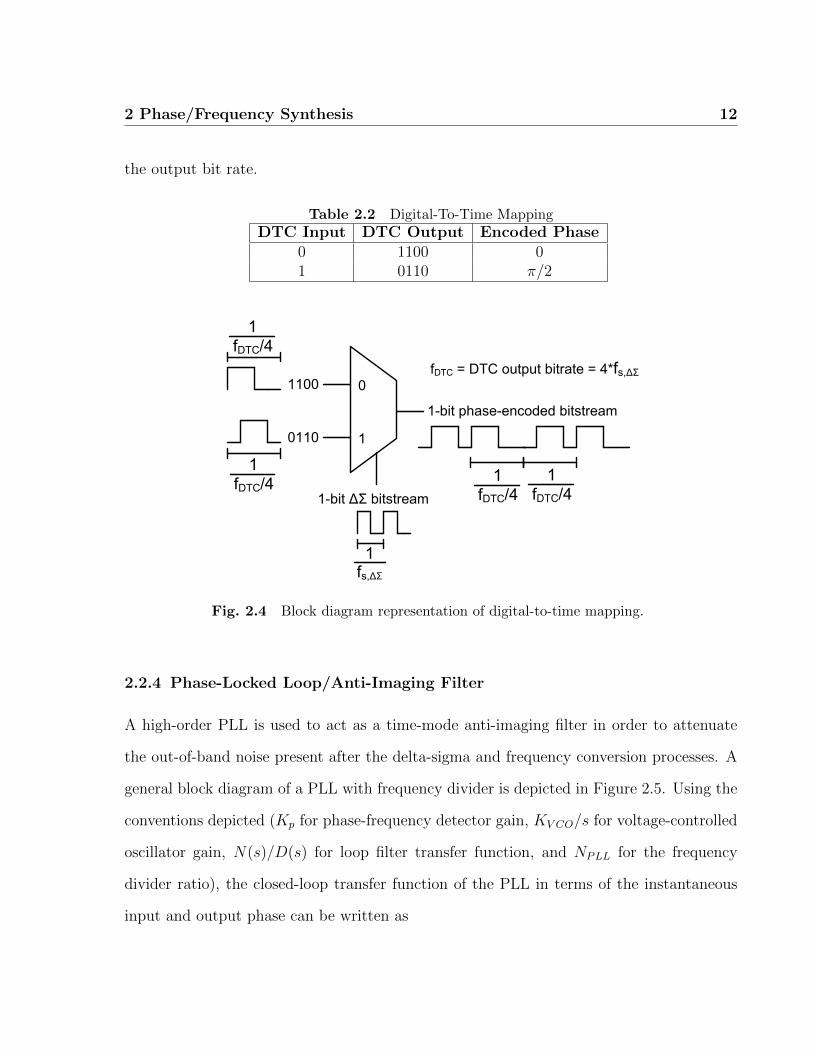
2 Phase/Frequency Synthesis 12
the output bit rate.
Table 2.2 Digital-To-Time MappingDTC Input DTC Output Encoded Phase
0 1100 01 0110 π/2
1100
0110 1
0
1-bit ΔΣ bitstream
1-bit phase-encoded bitstream
fDTC = DTC output bitrate = 4*fs,ΔΣ
fDTC/41
fDTC/41
fDTC/41
fDTC/41
fs,ΔΣ
1
Fig. 2.4 Block diagram representation of digital-to-time mapping.
2.2.4 Phase-Locked Loop/Anti-Imaging Filter
A high-order PLL is used to act as a time-mode anti-imaging filter in order to attenuate
the out-of-band noise present after the delta-sigma and frequency conversion processes. A
general block diagram of a PLL with frequency divider is depicted in Figure 2.5. Using the
conventions depicted (Kp for phase-frequency detector gain, KV CO/s for voltage-controlled
oscillator gain, N(s)/D(s) for loop filter transfer function, and NPLL for the frequency
divider ratio), the closed-loop transfer function of the PLL in terms of the instantaneous
input and output phase can be written as
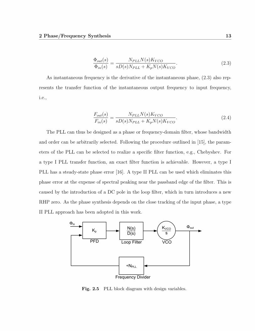
2 Phase/Frequency Synthesis 13
Φout(s)
Φin(s)=
NPLLN(s)KV CO
sD(s)NPLL +KpN(s)KV CO
. (2.3)
As instantaneous frequency is the derivative of the instantaneous phase, (2.3) also rep-
resents the transfer function of the instantaneous output frequency to input frequency,
i.e.,
Fout(s)
Fin(s)=
NPLLN(s)KV CO
sD(s)NPLL +KpN(s)KV CO
. (2.4)
The PLL can thus be designed as a phase or frequency-domain filter, whose bandwidth
and order can be arbitrarily selected. Following the procedure outlined in [15], the param-
eters of the PLL can be selected to realize a specific filter function, e.g., Chebyshev. For
a type I PLL transfer function, an exact filter function is achievable. However, a type I
PLL has a steady-state phase error [16]. A type II PLL can be used which eliminates this
phase error at the expense of spectral peaking near the passband edge of the filter. This is
caused by the introduction of a DC pole in the loop filter, which in turn introduces a new
RHP zero. As the phase synthesis depends on the close tracking of the input phase, a type
II PLL approach has been adopted in this work.
KpN(s)
D(s)
KVCO
s
÷NPLL
ΦinΦout
PFD Loop Filter VCO
Frequency Divider
Fig. 2.5 PLL block diagram with design variables.
2 Phase/Frequency Synthesis 14
2.2.5 Overall Phase/Frequency System Behaviour
Looking back at Figure 2.1 and the descriptions of each subsystem, it can be seen there
are certain design parameters to be manipulated in order to ensure the system operates
effectively. Both the delta-sigma modulator and PLL should have order and bandwidth
that closely correspond to each other. If the delta-sigma modulator has smaller bandwidth
than the PLL, quantization noise would be present at the output. Also, if the PLL order
is not high enough, then it may allow quantization noise to pass through. This is due to
the filter rolloff being too slow compared with the rate of rise of quantization noise with
frequency from the delta-sigma modulator.
The relationship linking the DFC output frequency fout and the DC input value (denoted
as DCin) to the delta-sigma modulator is given by
fout =fmax − fmin
∆Σmax −∆Σmin
DCin + fos (2.5)
where ∆Σmax and ∆Σmin are the maximum and minimum output levels of the delta-sigma
modulator, respectively.
In the case that a DTC is used, the relationship between the DC input DCin to the
delta-sigma modulator and the encoded output phase (φout) is given by
φout =φmax − φmin
∆Σmax −∆Σmin
DCin + φos (2.6)
The time delay of the output edge of the DTC with respect to the DTC output with zero
phase modulated signal can then be calculated from
tdelayi =φout
2π
1
fDTC
. (2.7)
2 Phase/Frequency Synthesis 15
The output phase delay, if there is no frequency divider in the feedback loop of the PLL
(i.e., NPLL = 1), would be equal to tdelayi . If NPLL 6= 0, the output phase delay is described
by the following equation:
tdelayo =mod(Nφout, 2π)
2π
1
NfDTC
. (2.8)
The modulo operation is due to the fact that the output frequency is faster than the
input frequency (carrier frequency of DTC). This results in an input delay that could exceed
the output period of the PLL, which would be accounted for by the modulo operation.
Once the modulator and PLL are designed, the desired frequency or phase is set by
changing the input DC level, as shown in (2.5) and (2.6). If a sine wave is input to the
system, then it will be phase or frequency modulated, depending on whether the DTC or
DFC is used.
2.3 Verification of Phase/Frequency System Behaviour
In order to verify the phase/frequency generation system, each block as shown in Figure
2.1 was implemented in Matlab and Simulink. The simulation results are then compared
to the theory to ensure the behaviour is as expected, for each subsystem and the entire
system as well.
2.3.1 Software-Based Delta-Sigma Modulator
A third-order delta-sigma modulator was implemented in Matlab. This allows for relatively
quick simulation and verification of any changes made to the modulator, such as bandwidth
or sampling frequency. The modulator was designed with a sampling frequency of 65 MHz,
an OSR of 16, resulting in a bandwidth of approximately 2 MHz. It was designed using
2 Phase/Frequency Synthesis 16
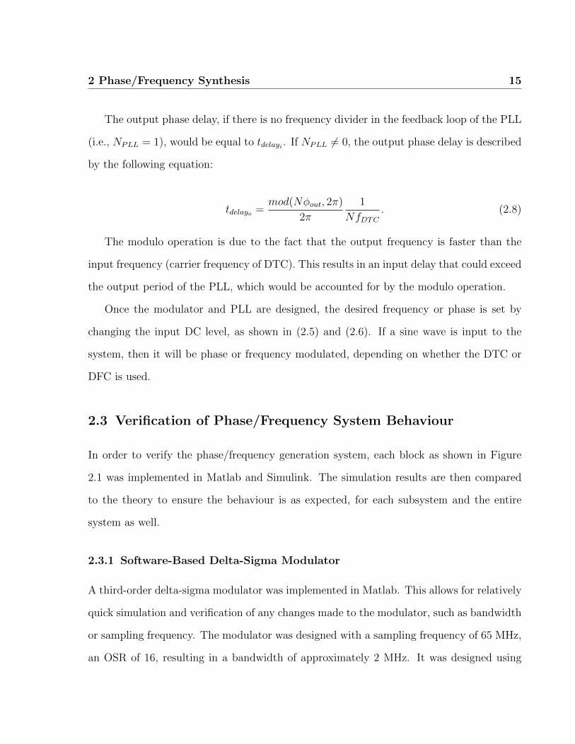
DSMOD [12] and simulated in Simulink using the state-space model shown in Figure 2.6.
The state-space coefficients are:
A =
3.967024151631377 −5.934175353815714 3.967024151631371 −0.999999999999997
1.000000000000000 0 0 0
0 1.000000000000000 0 0
0 0 1.000000000000000 0
B =
1
0
0
0
C =
[0.770057368795104 −2.036290740549418 1.826672124004636 −0.554374428267939
]
D = 0
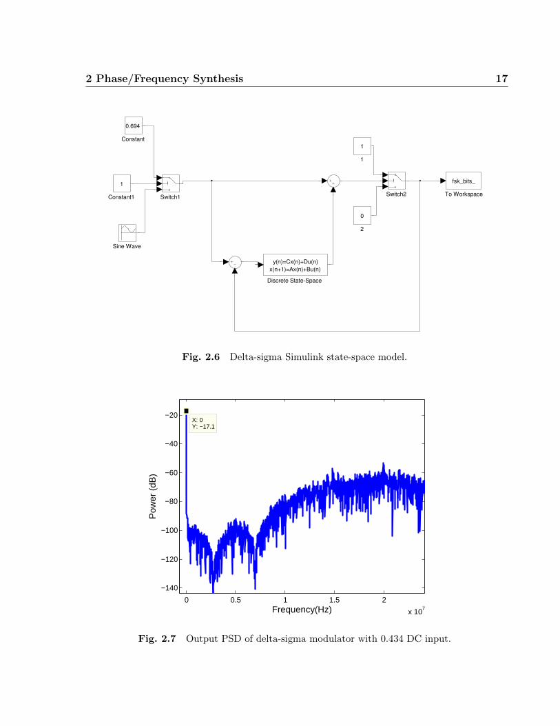
In Figure 2.6. Switch 1 provides the ability to switch between sine wave or DC input,
and Switch 2 acts like a 1-bit quantizer, encoding the output to either ”1” or “0” based on
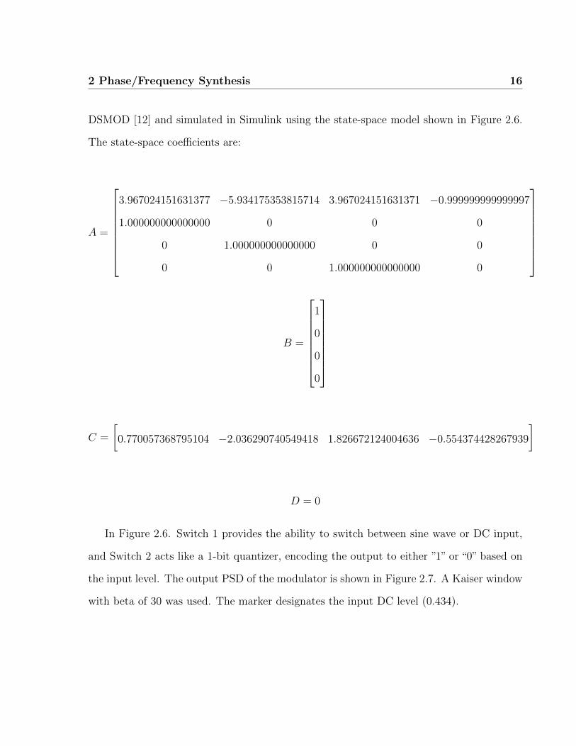
the input level. The output PSD of the modulator is shown in Figure 2.7. A Kaiser window
with beta of 30 was used. The marker designates the input DC level (0.434).
2 Phase/Frequency Synthesis 17
To Workspace
fsk_bits_
Switch2Switch1
Sine Wave
Discrete State-Space
y(n)=Cx(n)+Du(n)
x(n+1)=Ax(n)+Bu(n)
Constant1
1
Constant
0.694
2
0
1
1
Fig. 2.6 Delta-sigma Simulink state-space model.
0 0.5 1 1.5 2
x 107
−140
−120
−100
−80
−60
−40
−20X: 0Y: −17.1
Frequency(Hz)
Pow
er (
dB)
Fig. 2.7 Output PSD of delta-sigma modulator with 0.434 DC input.
2 Phase/Frequency Synthesis 18
2.3.2 DFC/DTC
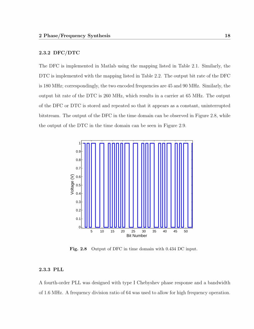
The DFC is implemented in Matlab using the mapping listed in Table 2.1. Similarly, the
DTC is implemented with the mapping listed in Table 2.2. The output bit rate of the DFC
is 180 MHz; correspondingly, the two encoded frequencies are 45 and 90 MHz. Similarly, the
output bit rate of the DTC is 260 MHz, which results in a carrier at 65 MHz. The output
of the DFC or DTC is stored and repeated so that it appears as a constant, uninterrupted
bitstream. The output of the DFC in the time domain can be observed in Figure 2.8, while
the output of the DTC in the time domain can be seen in Figure 2.9.
5 10 15 20 25 30 35 40 45 500
0.1
0.2
0.3
0.4
0.5
0.6
0.7
0.8
0.9
1
Vol
tage
(V
)
Bit Number
Fig. 2.8 Output of DFC in time domain with 0.434 DC input.
2.3.3 PLL
A fourth-order PLL was designed with type I Chebyshev phase response and a bandwidth
of 1.6 MHz. A frequency division ratio of 64 was used to allow for high frequency operation.
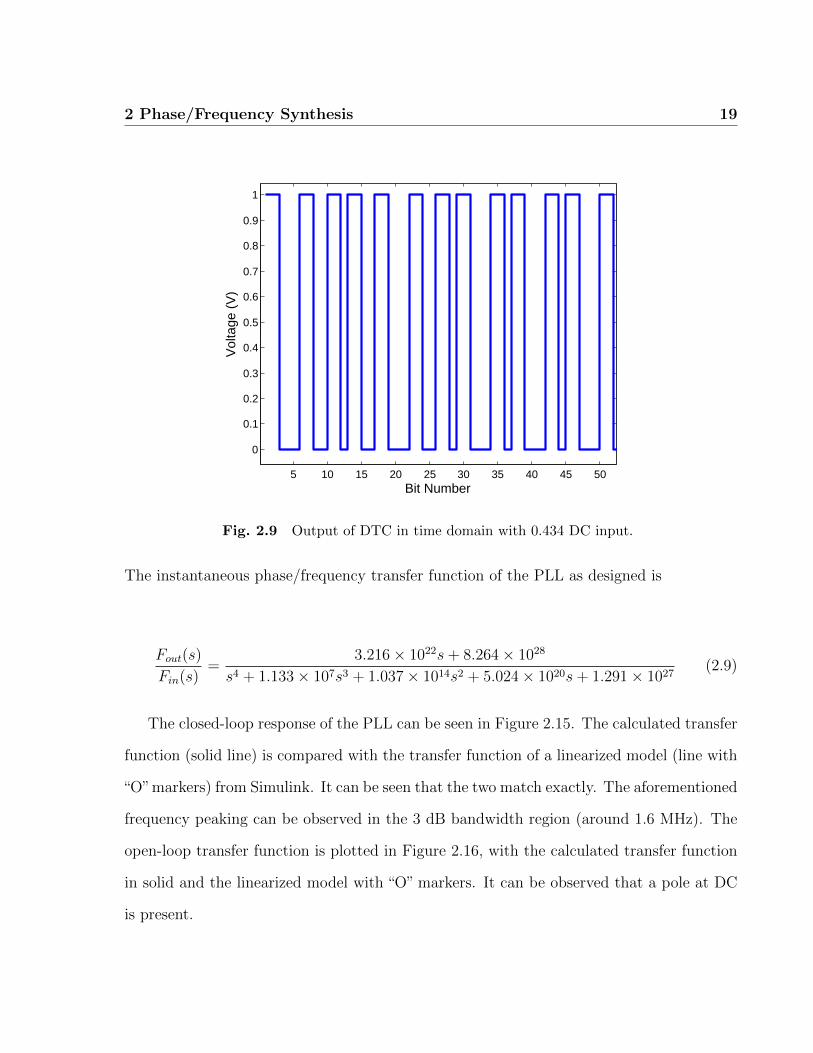
2 Phase/Frequency Synthesis 19
5 10 15 20 25 30 35 40 45 50
0
0.1
0.2
0.3
0.4
0.5
0.6
0.7
0.8
0.9
1
Vol
tage
(V
)
Bit Number
Fig. 2.9 Output of DTC in time domain with 0.434 DC input.
The instantaneous phase/frequency transfer function of the PLL as designed is
Fout(s)
Fin(s)=
3.216× 10²²s+ 8.264× 1028
s4 + 1.133× 10⁷s3 + 1.037× 10¹⁴s2 + 5.024× 10²⁰s+ 1.291× 1027(2.9)
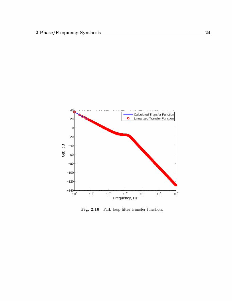
The closed-loop response of the PLL can be seen in Figure 2.15. The calculated transfer
function (solid line) is compared with the transfer function of a linearized model (line with
“O”markers) from Simulink. It can be seen that the two match exactly. The aforementioned
frequency peaking can be observed in the 3 dB bandwidth region (around 1.6 MHz). The
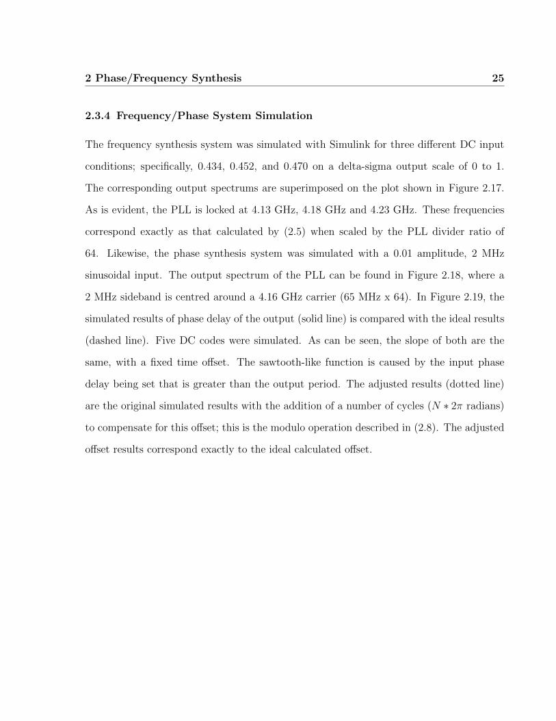
open-loop transfer function is plotted in Figure 2.16, with the calculated transfer function
in solid and the linearized model with “O” markers. It can be observed that a pole at DC
is present.
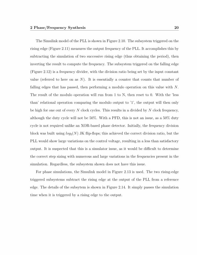
2 Phase/Frequency Synthesis 20
The Simulink model of the PLL is shown in Figure 2.10. The subsystem triggered on the
rising edge (Figure 2.11) measures the output frequency of the PLL. It accomplishes this by
subtracting the simulation of two successive rising edge (thus obtaining the period), then
inverting the result to compute the frequency. The subsystem triggered on the falling edge
(Figure 2.12) is a frequency divider, with the division ratio being set by the input constant
value (referred to here on as N). It is essentially a counter that counts that number of
falling edges that has passed, then performing a modulo operation on this value with N .
The result of the modulo operation will run from 1 to N, then reset to 0. With the ’less
than’ relational operation comparing the modulo output to ’1’, the output will then only
be high for one out of every N clock cycles. This results in a divided by N clock frequency,
although the duty cycle will not be 50%. With a PFD, this is not an issue, as a 50% duty
cycle is not required unlike an XOR-based phase detector. Initially, the frequency division
block was built using log2(N) JK flip-flops; this achieved the correct division ratio, but the
PLL would show large variations on the control voltage, resulting in a less than satisfactory
output. It is suspected that this is a simulator issue, as it would be difficult to determine
the correct step sizing with numerous and large variations in the frequencies present in the
simulation. Regardless, the subsystem shown does not have this issue.
For phase simulations, the Simulink model in Figure 2.13 is used. The two rising-edge
triggered subsystems subtract the rising edge at the output of the PLL from a reference
edge. The details of the subsytem is shown in Figure 2.14. It simply passes the simulation
time when it is triggered by a rising edge to the output.
2 Phase/Frequency Synthesis 21
Triggered
Subsystem
In1 Out1
Transfer Fcn
a(s)
b(s)
To Workspace1
simout1
Subsystem
div #Clock Out
Scope5
Scope3
Relay1
PFD
In1
In2
Out1
Math
Function
1
u
Gain1
.5From
Workspace
outputBitsOut
Continuous-Time
VCO1
Continuous-Time
VCO
Constant
64
Clock1
Fig. 2.10 PLL Simulink model with frequency measurement subsystem.
Out1
1
Unit Delay
z
1
Add
Trigger
In1
1
Fig. 2.11 Frequency measurement subsystem.
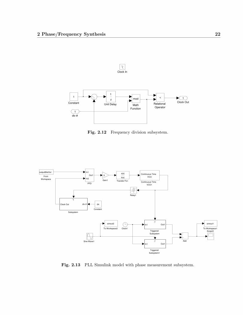
2 Phase/Frequency Synthesis 22
Clock Out
1
Unit Delay
z
1
Relational
Operator
<
Math
Function
mod
Constant
1
Clock In
div #
1
Fig. 2.12 Frequency division subsystem.
Triggered
Subsystem1
In1 Out1
Triggered
Subsystem
In1 Out1
Transfer Fcn
a(s)
b(s)
To Workspace2
simout2
To Workspace1
simout1
Subsystem
div #Clock Out
Sine Wave1
Scope3
Relay1
PFD
In1
In2
Out1
Gain1
.5From
Workspace
outputBitsOut
Continuous-Time
VCO1
Continuous-Time
VCO
Constant
64
Clock1
Add
Fig. 2.13 PLL Simulink model with phase measurement subsystem.
2 Phase/Frequency Synthesis 23
Out1
1
Trigger
In1
1
Fig. 2.14 Phase measurement subsystem.
102 103 104 105 106 1070
5
10
15
20
25
30
35
40
45
Frequency, Hz
G(f
), d
B
Calculated Transfer FunctionLinearized Transfer Function
Fig. 2.15 PLL closed-loop transfer function.
2 Phase/Frequency Synthesis 24
103 104 105 106 107 108 109−140
−120
−100
−80
−60
−40
−20
0
20
40
Frequency, Hz
G(f
), d
B
Calculated Transfer FunctionLinearized Transfer Function
Fig. 2.16 PLL loop filter transfer function.
2 Phase/Frequency Synthesis 25
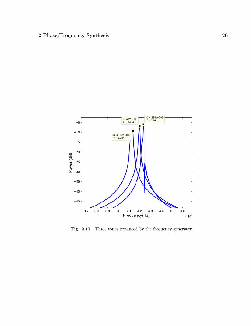
2.3.4 Frequency/Phase System Simulation
The frequency synthesis system was simulated with Simulink for three different DC input
conditions; specifically, 0.434, 0.452, and 0.470 on a delta-sigma output scale of 0 to 1.
The corresponding output spectrums are superimposed on the plot shown in Figure 2.17.
As is evident, the PLL is locked at 4.13 GHz, 4.18 GHz and 4.23 GHz. These frequencies
correspond exactly as that calculated by (2.5) when scaled by the PLL divider ratio of
64. Likewise, the phase synthesis system was simulated with a 0.01 amplitude, 2 MHz
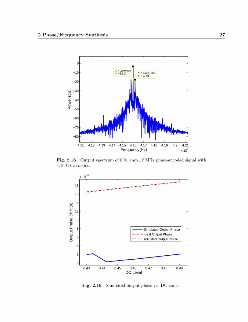
sinusoidal input. The output spectrum of the PLL can be found in Figure 2.18, where a
2 MHz sideband is centred around a 4.16 GHz carrier (65 MHz x 64). In Figure 2.19, the
simulated results of phase delay of the output (solid line) is compared with the ideal results
(dashed line). Five DC codes were simulated. As can be seen, the slope of both are the
same, with a fixed time offset. The sawtooth-like function is caused by the input phase
delay being set that is greater than the output period. The adjusted results (dotted line)
are the original simulated results with the addition of a number of cycles (N ∗ 2π radians)
to compensate for this offset; this is the modulo operation described in (2.8). The adjusted
offset results correspond exactly to the ideal calculated offset.
2 Phase/Frequency Synthesis 26
3.7 3.8 3.9 4 4.1 4.2 4.3 4.4 4.5 4.6
x 109
−45
−40
−35
−30
−25
−20
−15
−10
−5X: 4.2e+009Y: −6.651
Frequency(Hz)
Pow
er (
dB)
X: 4.234e+009Y: −5.94
X: 4.137e+009Y: −9.254
Fig. 2.17 Three tones produced by the frequency generator.
2 Phase/Frequency Synthesis 27
4.11 4.12 4.13 4.14 4.15 4.16 4.17 4.18 4.19 4.2 4.21
x 109
−80
−70
−60
−50
−40
−30
−20
−10
0
X: 4.16e+009Y: −3.512
Frequency(Hz)
Pow
er (
dB)
X: 4.162e+009Y: −17.91
Fig. 2.18 Output spectrum of 0.01 amp., 2 MHz phase-encoded signal with4.16 GHz carrier.
0.43 0.44 0.45 0.46 0.47 0.48 0.49
0
2
4
6
8
10
12
14
16
18
x 10−10
DC Level
Out
put P
hase
Shi
ft (s
)
Simulated Output PhaseIdeal Output PhaseAdjusted Output Phase
Fig. 2.19 Simulated output phase vs. DC code.
2 Phase/Frequency Synthesis 28
2.4 Summary
The phase/frequency signal generation system is presented. The subsystems consist of a
software-based delta-sigma modulator, a digital-to-time or digital-to-frequency converter,
followed by a PLL. The system is verified in Simulink, and the results compared with
theoretical values. Each subsystem and the phase/frequency generation system as a whole
behaves as predicted by design.
29
Chapter 3
PLL Design
In order to test frequency and phase synthesis at high speeds, a custom PLL had to be
designed and built. A top-down design methodology was employed to impose a desired
phase transfer function, as described in Section 2.2.4. The IBM cmrf8sf 130 nm process
(cmosp13) was chosen as the technology for fabrication, due to its maturity as well as its
preferred status with CMC [17]. Each PLL block was then implemented on a transistor level
using the Cadence Design Environment, and the functionality was verified using Spectre.
3.1 Transistor-Level Design
After the phase transfer function of the PLL has been determined, each component of the
PLL was designed and implemented at the transistor level using Cadence. A general block
diagram of the components comprising a typical charge pump PLL is shown in Figure 3.1.
3 PLL Design 30
Phase-
Frequency
DetectorCharge Pump Loop Filter
Voltage
Controlled
Oscillator
Frequency
Divider(s)
Fref
Output
Fig. 3.1 General block diagram of charge pump PLL.
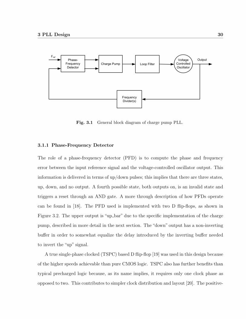
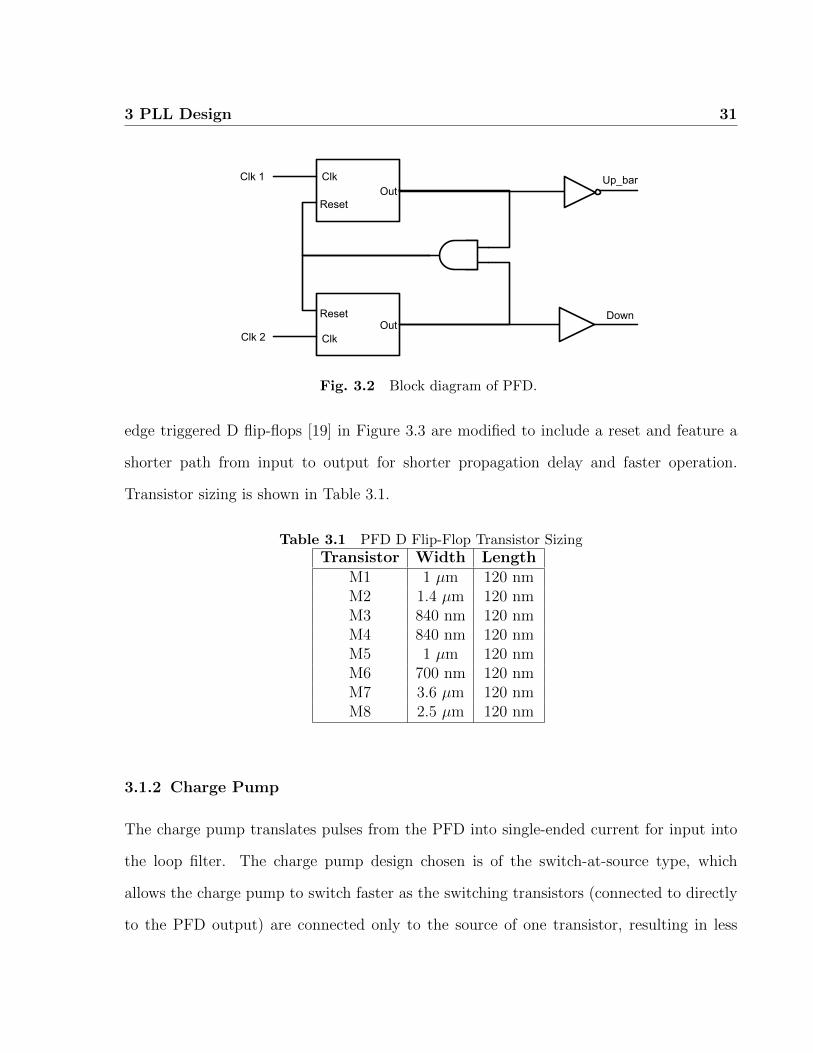
3.1.1 Phase-Frequency Detector
The role of a phase-frequency detector (PFD) is to compute the phase and frequency
error between the input reference signal and the voltage-controlled oscillator output. This
information is delivered in terms of up/down pulses; this implies that there are three states,
up, down, and no output. A fourth possible state, both outputs on, is an invalid state and
triggers a reset through an AND gate. A more through description of how PFDs operate
can be found in [18]. The PFD used is implemented with two D flip-flops, as shown in
Figure 3.2. The upper output is “up bar” due to the specific implementation of the charge
pump, described in more detail in the next section. The “down” output has a non-inverting
buffer in order to somewhat equalize the delay introduced by the inverting buffer needed
to invert the “up” signal.
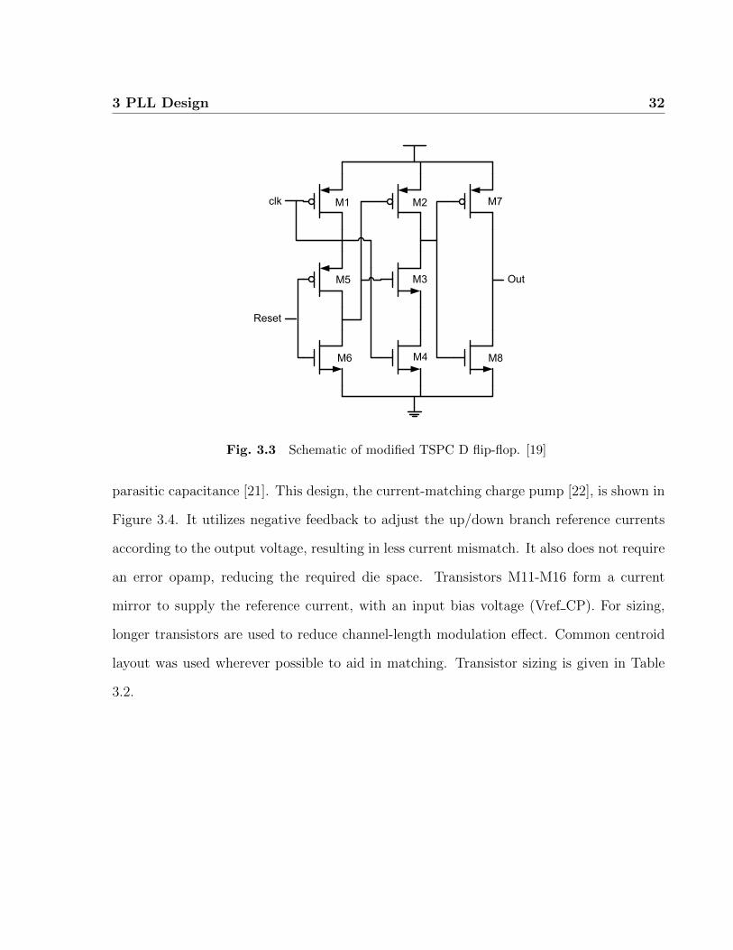
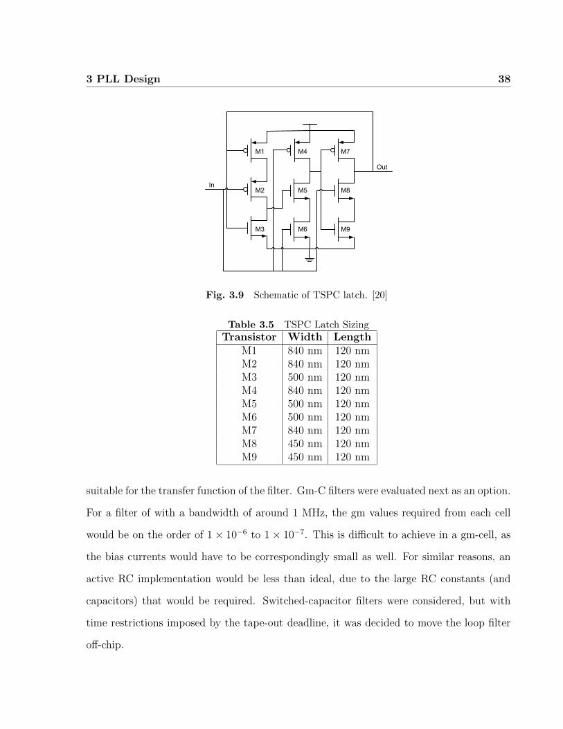
A true single-phase clocked (TSPC) based D flip-flop [19] was used in this design because
of the higher speeds achievable than pure CMOS logic. TSPC also has further benefits than
typical precharged logic because, as its name implies, it requires only one clock phase as
opposed to two. This contributes to simpler clock distribution and layout [20]. The positive-
3 PLL Design 31
Clk
Reset
Out
Clk
ResetOut
Clk 1
Clk 2
Up_bar
Down
Fig. 3.2 Block diagram of PFD.
edge triggered D flip-flops [19] in Figure 3.3 are modified to include a reset and feature a
shorter path from input to output for shorter propagation delay and faster operation.
Transistor sizing is shown in Table 3.1.
Table 3.1 PFD D Flip-Flop Transistor SizingTransistor Width Length
M1 1 µm 120 nmM2 1.4 µm 120 nmM3 840 nm 120 nmM4 840 nm 120 nmM5 1 µm 120 nmM6 700 nm 120 nmM7 3.6 µm 120 nmM8 2.5 µm 120 nm
3.1.2 Charge Pump
The charge pump translates pulses from the PFD into single-ended current for input into
the loop filter. The charge pump design chosen is of the switch-at-source type, which
allows the charge pump to switch faster as the switching transistors (connected to directly
to the PFD output) are connected only to the source of one transistor, resulting in less
3 PLL Design 32
clk
Reset
Out
M1 M2
M3
M4
M5
M6
M7
M8
Fig. 3.3 Schematic of modified TSPC D flip-flop. [19]
parasitic capacitance [21]. This design, the current-matching charge pump [22], is shown in
Figure 3.4. It utilizes negative feedback to adjust the up/down branch reference currents
according to the output voltage, resulting in less current mismatch. It also does not require
an error opamp, reducing the required die space. Transistors M11-M16 form a current
mirror to supply the reference current, with an input bias voltage (Vref CP). For sizing,
longer transistors are used to reduce channel-length modulation effect. Common centroid
layout was used wherever possible to aid in matching. Transistor sizing is given in Table
3.2.
3 PLL Design 33
Up_bar
Down
CP_out
Vref_CP
M1 M2
M3
M4
M5 M6
M7
M8
M9
M10
M11
M12
M13
M14
M15
M16
Fig. 3.4 Schematic of charge pump. [23]
Table 3.2 Charge Pump Transistor SizingTransistor Width Length
M1 1.4 µm 120 nmM2 500 nm 120 nmM3 3.8 µm 120 nmM4 8.6 µm 240 nmM5 2.5 µm 240 nmM6 1 µm 120 nmM7 2.8 µm 240 nmM8 8.6 µm 240 nmM9 2.5 µm 240 nmM10 1 µm 120 nmM11 2.8 µm 240 nmM12 1 µm 240 nmM13 2.8 µm 240 nmM14 1 µm 240 nmM15 2.8 µm 240 nmM16 1 µm 240 nm
3 PLL Design 34
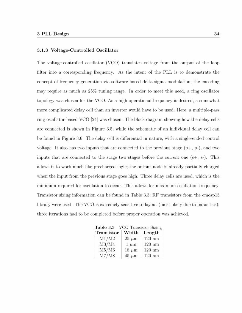
3.1.3 Voltage-Controlled Oscillator
The voltage-controlled oscillator (VCO) translates voltage from the output of the loop
filter into a corresponding frequency. As the intent of the PLL is to demonstrate the
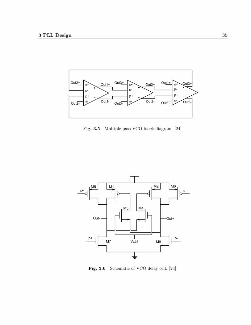
concept of frequency generation via software-based delta-sigma modulation, the encoding
may require as much as 25% tuning range. In order to meet this need, a ring oscillator
topology was chosen for the VCO. As a high operational frequency is desired, a somewhat
more complicated delay cell than an inverter would have to be used. Here, a multiple-pass
ring oscillator-based VCO [24] was chosen. The block diagram showing how the delay cells
are connected is shown in Figure 3.5, while the schematic of an individual delay cell can
be found in Figure 3.6. The delay cell is differential in nature, with a single-ended control
voltage. It also has two inputs that are connected to the previous stage (p+, p-), and two
inputs that are connected to the stage two stages before the current one (s+, s-). This
allows it to work much like precharged logic; the output node is already partially charged
when the input from the previous stage goes high. Three delay cells are used, which is the
minimum required for oscillation to occur. This allows for maximum oscillation frequency.
Transistor sizing information can be found in Table 3.3; RF transistors from the cmosp13
library were used. The VCO is extremely sensitive to layout (most likely due to parasitics);
three iterations had to be completed before proper operation was achieved.
Table 3.3 VCO Transistor SizingTransistor Width Length
M1/M2 25 µm 120 nmM3/M4 1 µm 120 nmM5/M6 18 µm 120 nmM7/M8 45 µm 120 nm
3 PLL Design 35
s+
p+
p-
s-
s+
p+
p-
s-
s+
p+
p-
s-
Out1+ Out2+ Out3+
Out1- Out2- Out3-
Out1+
Out1-
Out3+
Out3-
Out2+
Out2-
Fig. 3.5 Multiple-pass VCO block diagram. [24]
Vctrl
Out+Out-
s-s+
p-p+
M5 M1 M2 M6
M3 M4
M7 M8
Fig. 3.6 Schematic of VCO delay cell. [24]
3 PLL Design 36
3.1.4 Frequency Divider
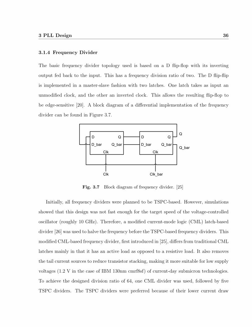
The basic frequency divider topology used is based on a D flip-flop with its inverting
output fed back to the input. This has a frequency division ratio of two. The D flip-flip
is implemented in a master-slave fashion with two latches. One latch takes as input an
unmodified clock, and the other an inverted clock. This allows the resulting flip-flop to
be edge-sensitive [20]. A block diagram of a differential implementation of the frequency
divider can be found in Figure 3.7.
Q
Q_bar
Clk
D
D_bar
Q
Q_bar
Clk
D
D_bar
Clk Clk_bar
Q
Q_bar
Fig. 3.7 Block diagram of frequency divider. [25]
Initially, all frequency dividers were planned to be TSPC-based. However, simulations
showed that this design was not fast enough for the target speed of the voltage-controlled
oscillator (roughly 10 GHz). Therefore, a modified current-mode logic (CML) latch-based
divider [26] was used to halve the frequency before the TSPC-based frequency dividers. This
modified CML-based frequency divider, first introduced in [25], differs from traditional CML
latches mainly in that it has an active load as opposed to a resistive load. It also removes
the tail current sources to reduce transistor stacking, making it more suitable for low supply
voltages (1.2 V in the case of IBM 130nm cmrf8sf) of current-day submicron technologies.
To achieve the designed division ratio of 64, one CML divider was used, followed by five
TSPC dividers. The TSPC dividers were preferred because of their lower current draw
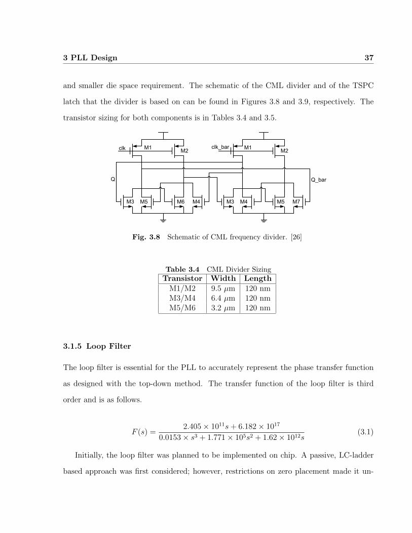
3 PLL Design 37
and smaller die space requirement. The schematic of the CML divider and of the TSPC
latch that the divider is based on can be found in Figures 3.8 and 3.9, respectively. The
transistor sizing for both components is in Tables 3.4 and 3.5.
clk clk_bar
Q Q_bar
M1M2
M3 M5 M6 M4
M1M2
M3 M4 M5 M7
Fig. 3.8 Schematic of CML frequency divider. [26]
Table 3.4 CML Divider SizingTransistor Width Length
M1/M2 9.5 µm 120 nmM3/M4 6.4 µm 120 nmM5/M6 3.2 µm 120 nm
3.1.5 Loop Filter
The loop filter is essential for the PLL to accurately represent the phase transfer function
as designed with the top-down method. The transfer function of the loop filter is third
order and is as follows.
F (s) =2.405× 10¹¹s+ 6.182× 10¹⁷
0.0153× s3 + 1.771× 10⁵s2 + 1.62× 10¹²s(3.1)
Initially, the loop filter was planned to be implemented on chip. A passive, LC-ladder
based approach was first considered; however, restrictions on zero placement made it un-
3 PLL Design 38
In
Out
M1
M2
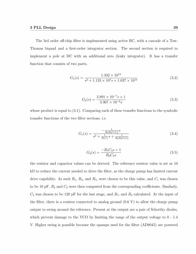
M3
M4
M5
M6
M7
M8
M9
Fig. 3.9 Schematic of TSPC latch. [20]
Table 3.5 TSPC Latch SizingTransistor Width Length
M1 840 nm 120 nmM2 840 nm 120 nmM3 500 nm 120 nmM4 840 nm 120 nmM5 500 nm 120 nmM6 500 nm 120 nmM7 840 nm 120 nmM8 450 nm 120 nmM9 450 nm 120 nm
suitable for the transfer function of the filter. Gm-C filters were evaluated next as an option.
For a filter of with a bandwidth of around 1 MHz, the gm values required from each cell
would be on the order of 1× 10⁻⁶ to 1× 10⁻⁷. This is difficult to achieve in a gm-cell, as
the bias currents would have to be correspondingly small as well. For similar reasons, an
active RC implementation would be less than ideal, due to the large RC constants (and
capacitors) that would be required. Switched-capacitor filters were considered, but with
time restrictions imposed by the tape-out deadline, it was decided to move the loop filter
off-chip.
3 PLL Design 39
The 3rd order off-chip filter is implemented using active RC, with a cascade of a Tow-
Thomas biquad and a first-order integrator section. The second section is required to
implement a pole at DC with an additional zero (leaky integrator). It has a transfer
function that consists of two parts,
G1(s) =1.332× 10¹⁴
s2 + 1.133× 10⁷s+ 1.037× 10¹⁴(3.2)
G2(s) =3.891× 10⁻⁷s+ 1
3.367× 10⁻⁶s(3.3)
whose product is equal to (3.1). Comparing each of these transfer functions to the symbolic
transfer functions of the two filter sections, i.e.
G1(s) =− 1
R2R4C1C2s
s2 + 1R1C1
s+ 1R2R3C1C2
(3.4)
G2(s) =−R7C3s+ 1
R8C3s(3.5)
the resistor and capacitor values can be derived. The reference resistor value is set at 10
kΩ to reduce the current needed to drive the filter, as the charge pump has limited current
drive capability. As such R1, R3, and R4, were chosen to be this value, and C1 was chosen
to be 10 pF. R2 and C2 were then computed from the corresponding coefficients. Similarly,
C3 was chosen to be 120 pF for the last stage, and R7, and R3 calculated. At the input of
the filter, there is a resistor connected to analog ground (0.6 V) to allow the charge pump
output to swing around the reference. Present at the output are a pair of Schottky diodes,
which prevent damage to the VCO by limiting the range of the output voltage to 0 - 1.4
V. Higher swing is possible because the opamps used for the filter (AD8045) are powered
3 PLL Design 40
from +/-5 V. The component values are summarized in Table 3.6.
R10
R4
R1
R2R5
R6
R3
R8
R9
C3
C2
C1
CP_out
Agnd Vctrl
0V
AVDD
Agnd
R7
AgndAgnd
Agnd
Fig. 3.10 Loop filter schematic. [27], [16]
Table 3.6 Loop Filter Component ValuesName ValueR1 10 kΩR2 10 kΩR3 12.7 kΩR4 10 kΩR5 10 kΩR6 10 kΩR7 28 kΩR8 3.24 kΩR9 1 kΩR10 10 kΩC1 10 pFC2 10 pFC3 120 pF
3.1.6 Input/Output Circuitry
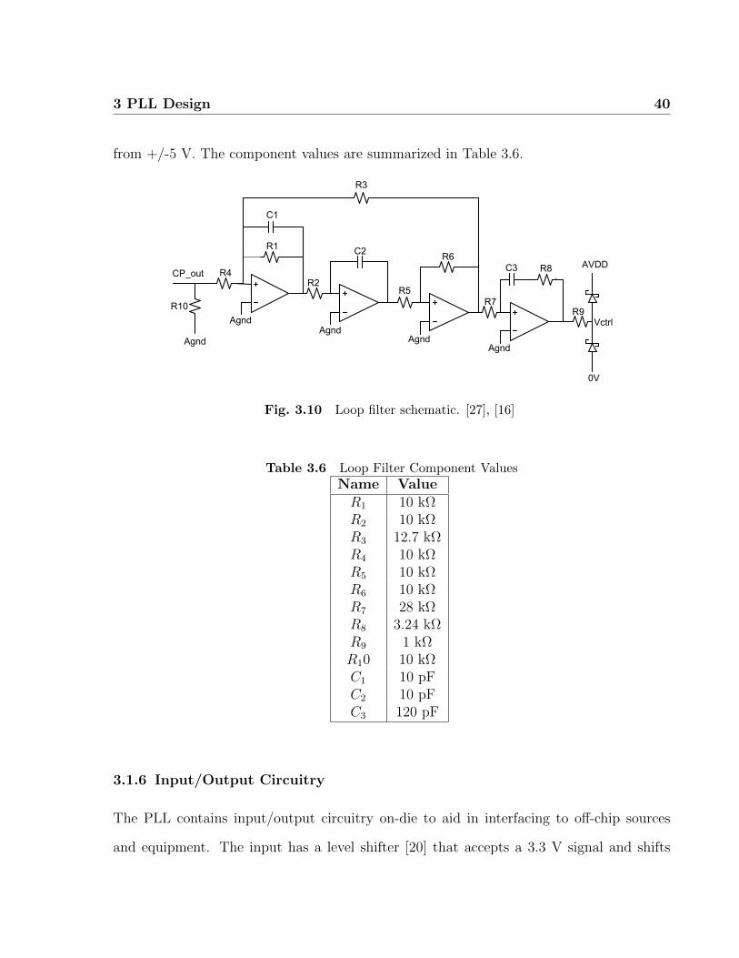
The PLL contains input/output circuitry on-die to aid in interfacing to off-chip sources
and equipment. The input has a level shifter [20] that accepts a 3.3 V signal and shifts
3 PLL Design 41
it down to 1.2 V for the PFD input. The 3.3 V I/O (thick-oxide) transistors used at the
input of the level shifter also has a larger maximum allowed VDS before breakdown than
standard 1.2 V transistors, allowing for a larger margin of error when connecting or setting
up input sources. The level shifter also passes a 1.2 V input signal. The circuit diagram
can be found in Figure 3.11, while the transistor sizing is found in Table 3.7.
InOut
M1
M2
M3
M4
Fig. 3.11 Input buffer schematic. [28]
Table 3.7 Input Buffer SizingTransistor Width Length
M1 1.7 µm 400 nmM2 600 nm 400 nmM3 3 µm 400 nmM4 1.1 µm 400 nm
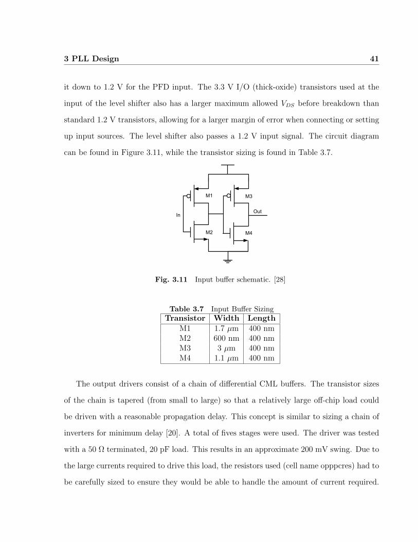
The output drivers consist of a chain of differential CML buffers. The transistor sizes
of the chain is tapered (from small to large) so that a relatively large off-chip load could
be driven with a reasonable propagation delay. This concept is similar to sizing a chain of
inverters for minimum delay [20]. A total of fives stages were used. The driver was tested
with a 50 Ω terminated, 20 pF load. This results in an approximate 200 mV swing. Due to
the large currents required to drive this load, the resistors used (cell name opppcres) had to
be carefully sized to ensure they would be able to handle the amount of current required.
3 PLL Design 42
These polysilicon resistors were chosen because of their low variability over voltage and
temperature. The maximum allowed current for opppcres is 0.4 mA/µm in width [29]. The
schematic of a single CML buffer stage can be found in Figure 3.12. The transistor sizing
for each stage can be found in Table 3.8, while the resistor values for each stage is found
in Table 3.9.
Vin+ Vin-
Vbias
Vout+Vout-
M1 M2
M3
RD RD
Fig. 3.12 CML buffer schematic. [30]
Table 3.8 CML Buffer Transistor SizingStage Transistor Width Length
1M1/M2 4 µm 120 nm
M3 10 µm 1 µm
2M1/M2 6 µm 120 nm
M3 20 µm 1 µm
3M1/M2 16 µm 120 nm
M3 65 µm 1 µm
4M1/M2 20 µm 120 nm
M3 100 µm 1 µm
5M1/M2 40 µm 120 nm
M3 210 µm 1 µm
3 PLL Design 43
Table 3.9 CML Buffer Resistor ValuesStage Value
1 1.234 kΩ2 663 Ω3 227 Ω4 154 Ω5 74 Ω
3.2 Layout
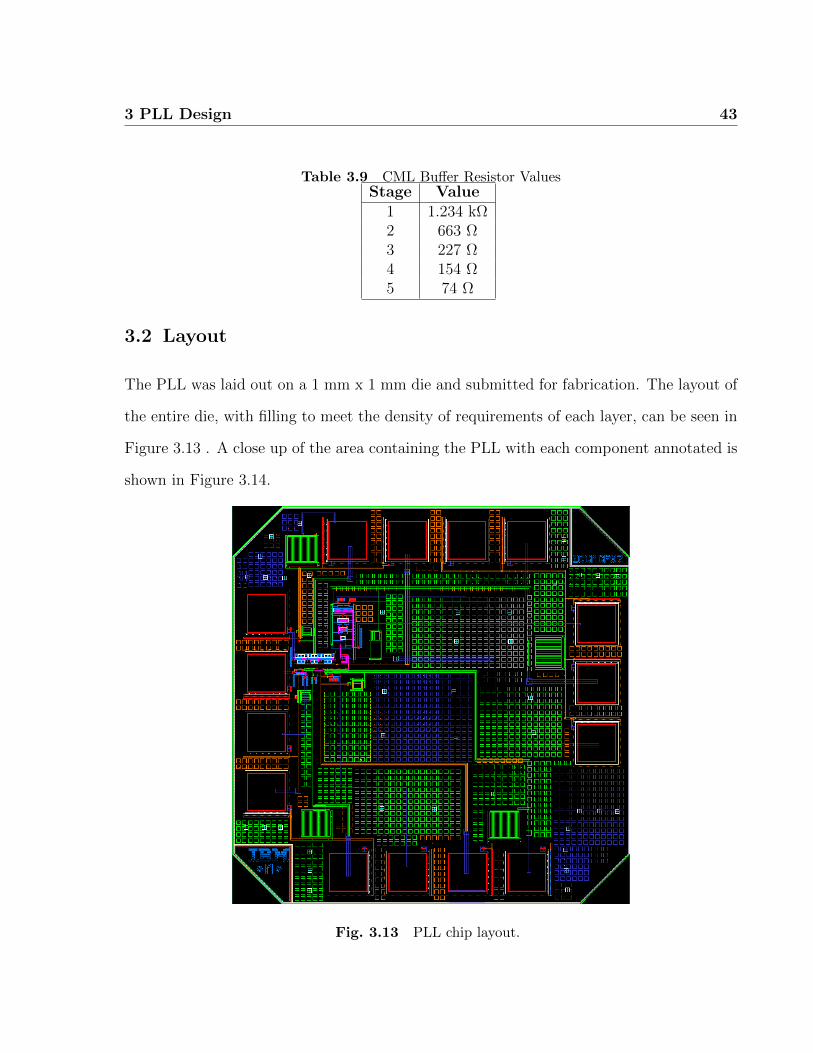
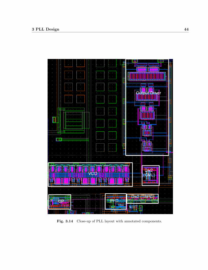
The PLL was laid out on a 1 mm x 1 mm die and submitted for fabrication. The layout of
the entire die, with filling to meet the density of requirements of each layer, can be seen in
Figure 3.13 . A close up of the area containing the PLL with each component annotated is
shown in Figure 3.14.
Fig. 3.13 PLL chip layout.
3 PLL Design 44
Fig. 3.14 Close-up of PLL layout with annotated components.
3 PLL Design 45
3.3 Transistor-Level Simulations
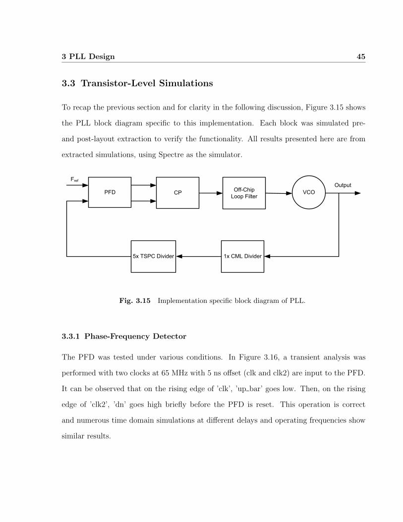
To recap the previous section and for clarity in the following discussion, Figure 3.15 shows
the PLL block diagram specific to this implementation. Each block was simulated pre-
and post-layout extraction to verify the functionality. All results presented here are from
extracted simulations, using Spectre as the simulator.
PFD CPOff-Chip
Loop FilterVCO
1x CML Divider5x TSPC Divider
Fref
Output
Fig. 3.15 Implementation specific block diagram of PLL.
3.3.1 Phase-Frequency Detector
The PFD was tested under various conditions. In Figure 3.16, a transient analysis was
performed with two clocks at 65 MHz with 5 ns offset (clk and clk2) are input to the PFD.
It can be observed that on the rising edge of ’clk’, ’up bar’ goes low. Then, on the rising
edge of ’clk2’, ’dn’ goes high briefly before the PFD is reset. This operation is correct
and numerous time domain simulations at different delays and operating frequencies show
similar results.
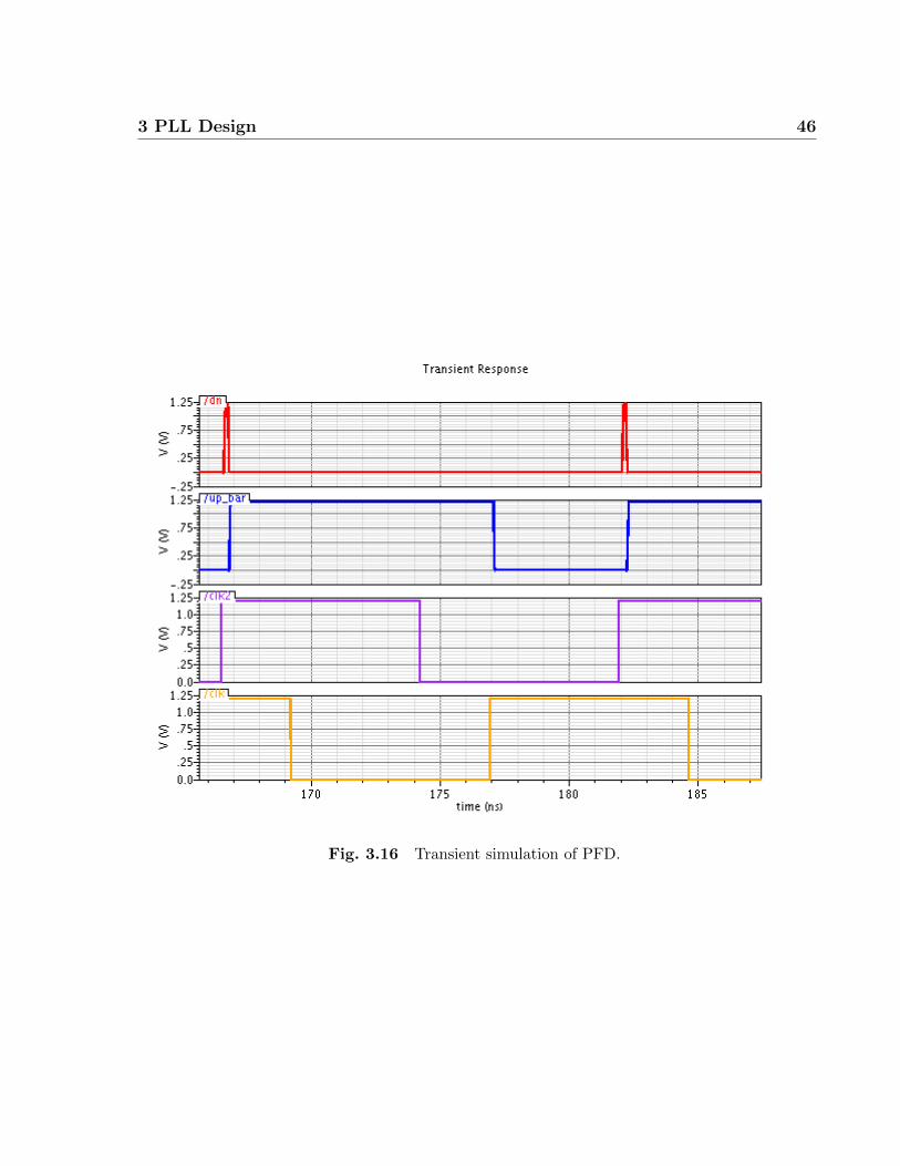
3 PLL Design 46
Fig. 3.16 Transient simulation of PFD.
3 PLL Design 47
3.3.2 Charge Pump
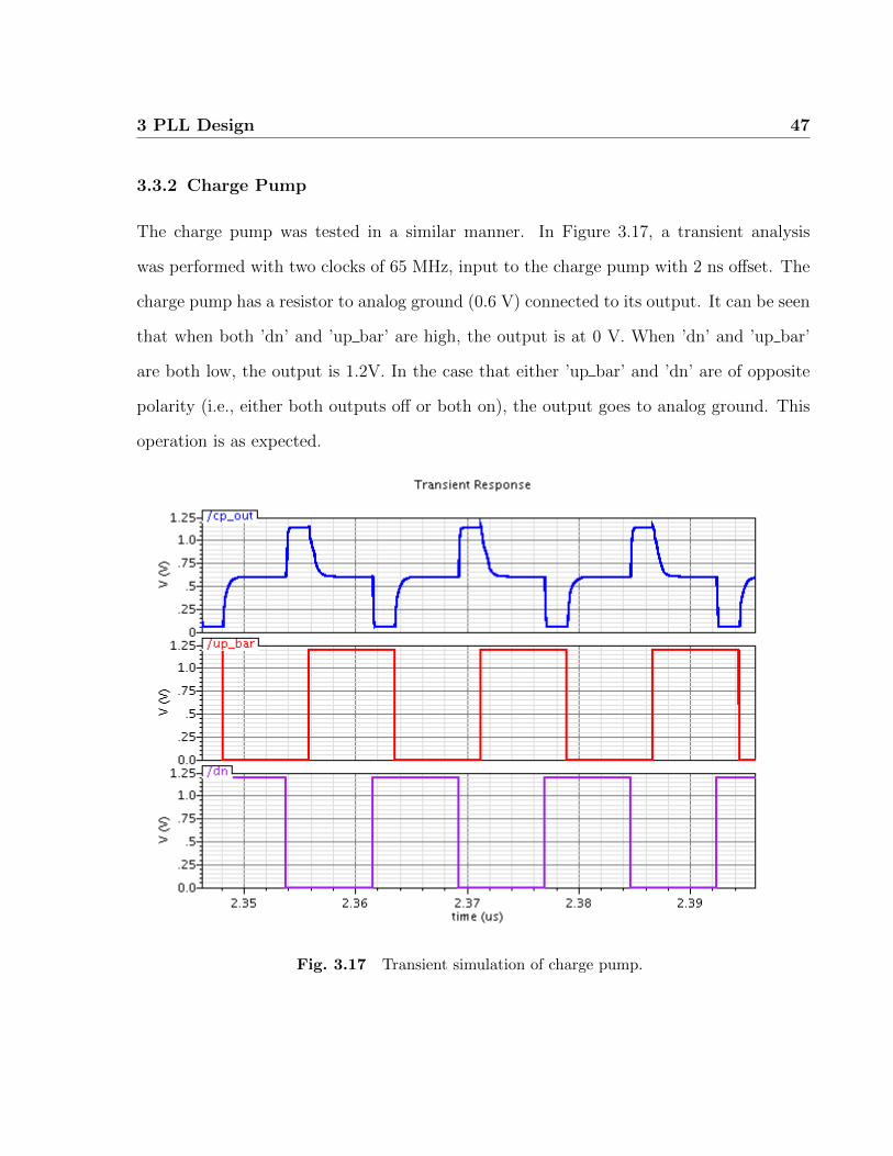
The charge pump was tested in a similar manner. In Figure 3.17, a transient analysis
was performed with two clocks of 65 MHz, input to the charge pump with 2 ns offset. The
charge pump has a resistor to analog ground (0.6 V) connected to its output. It can be seen
that when both ’dn’ and ’up bar’ are high, the output is at 0 V. When ’dn’ and ’up bar’
are both low, the output is 1.2V. In the case that either ’up bar’ and ’dn’ are of opposite
polarity (i.e., either both outputs off or both on), the output goes to analog ground. This
operation is as expected.
Fig. 3.17 Transient simulation of charge pump.
3 PLL Design 48
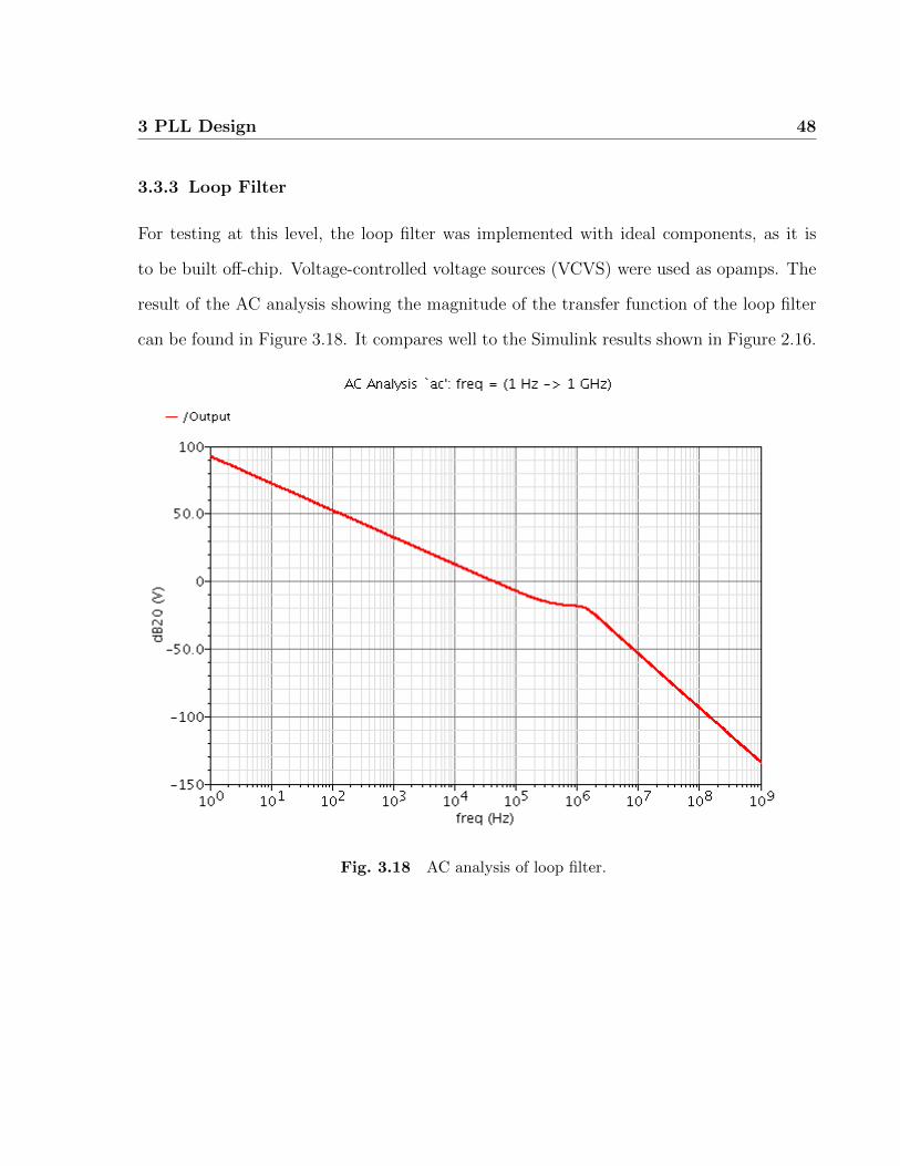
3.3.3 Loop Filter
For testing at this level, the loop filter was implemented with ideal components, as it is
to be built off-chip. Voltage-controlled voltage sources (VCVS) were used as opamps. The
result of the AC analysis showing the magnitude of the transfer function of the loop filter
can be found in Figure 3.18. It compares well to the Simulink results shown in Figure 2.16.
Fig. 3.18 AC analysis of loop filter.
3 PLL Design 49
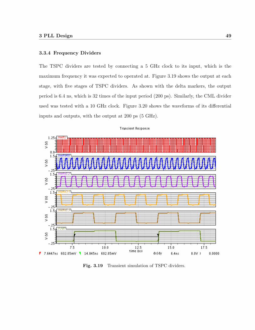
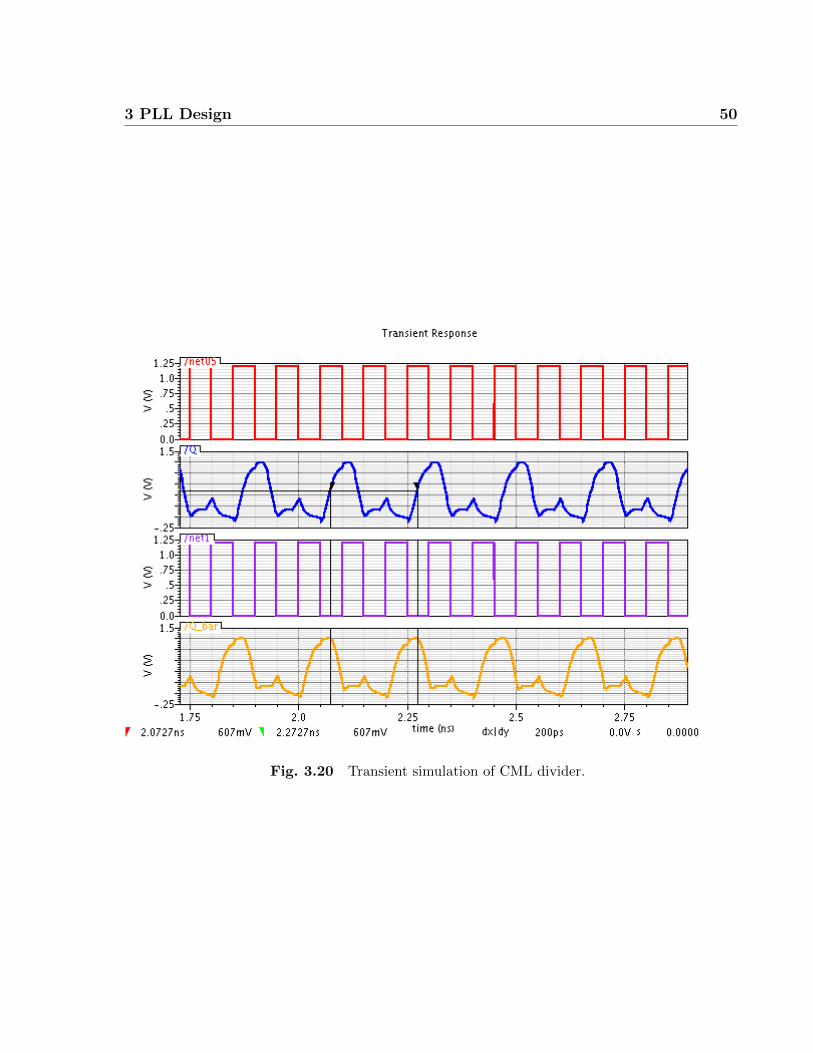
3.3.4 Frequency Dividers
The TSPC dividers are tested by connecting a 5 GHz clock to its input, which is the
maximum frequency it was expected to operated at. Figure 3.19 shows the output at each
stage, with five stages of TSPC dividers. As shown with the delta markers, the output
period is 6.4 ns, which is 32 times of the input period (200 ps). Similarly, the CML divider
used was tested with a 10 GHz clock. Figure 3.20 shows the waveforms of its differential
inputs and outputs, with the output at 200 ps (5 GHz).
Fig. 3.19 Transient simulation of TSPC dividers.
3 PLL Design 50
Fig. 3.20 Transient simulation of CML divider.
3 PLL Design 51
3.3.5 Voltage-Controlled Oscillator
The VCO transient simulation results can be seen in Figure 3.21. The control voltage was
800 mV, which resulted in an output frequency of approximately 8.5 GHz (period of 117 ps
as shown with the delta marker). The VCO output is roughly sinusoidal. The gain of the
VCO was calculated by computing the frequency point-by-point from sweeping the control
voltage, then obtaining the slope of a best-fit line through these points. The results are
plotted using Excel and can be seen in Figure 3.22. The VCO gain is -4 GHz/V roughly.
The VCO phase noise versus frequency offset was computed using a PSS and PNOISE
analysis under SpectreRF, with the same input conditions used in the transient simulation.
The result can be seen in Figure 3.23. The phase noise at 1 MHz offset from the carrier is
-81.86 dBc/Hz.
3 PLL Design 52
Fig. 3.21 Transient simulation of VCO.
3 PLL Design 53
7.50E+09
8.00E+09
8.50E+09
9.00E+09
9.50E+09
Frequency (Hz) vs. Input Voltage (V)
Freq
Linear (Freq)
y = -4E+09x + 1E+10
6.00E+09
6.50E+09
7.00E+09
7.50E+09
8.00E+09
8.50E+09
9.00E+09
9.50E+09
0.3 0.4 0.5 0.6 0.7 0.8 0.9 1 1.1 1.2 1.3
Frequency (Hz) vs. Input Voltage (V)
Freq
Linear (Freq)
Fig. 3.22 VCO output frequency versus input voltage.
3 PLL Design 54
Fig. 3.23 PNOISE simulation of VCO.
3 PLL Design 55
3.3.6 Input/Output Circuitry
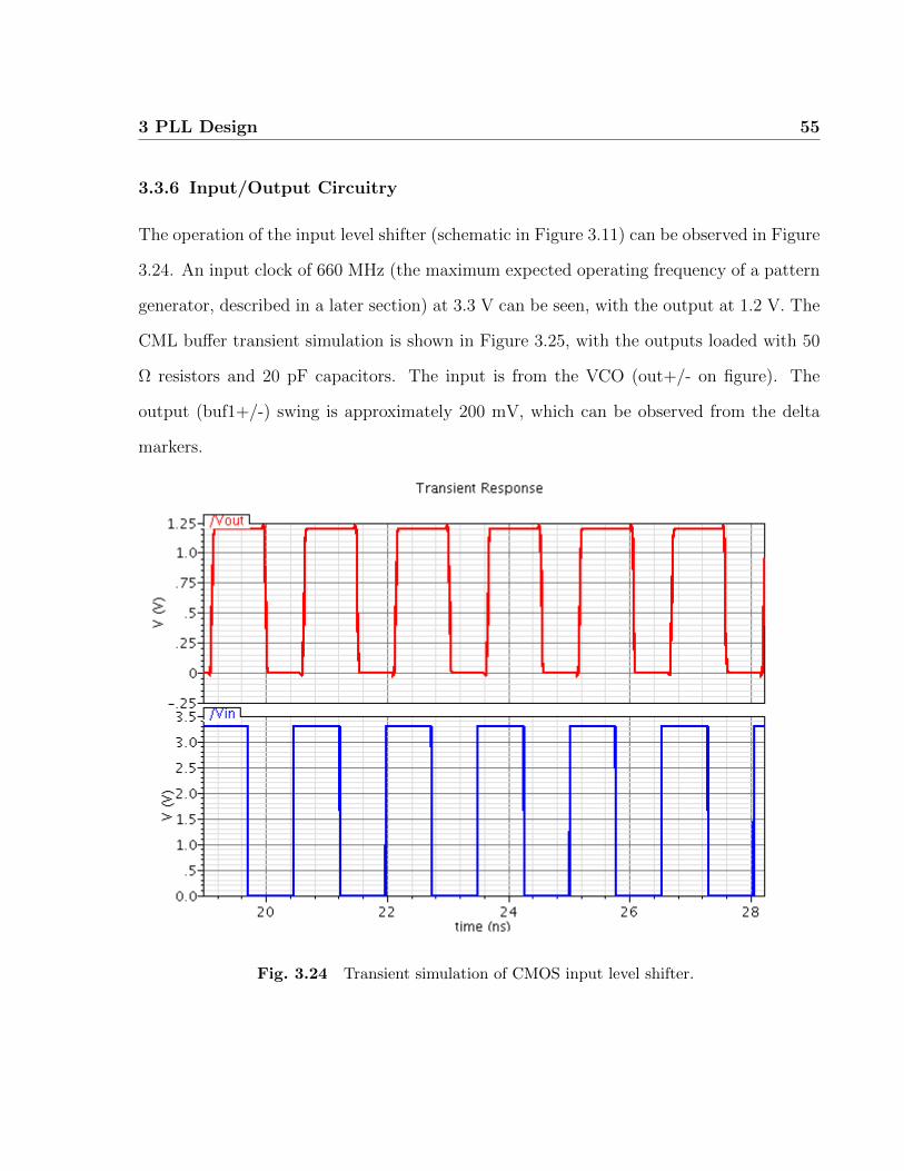
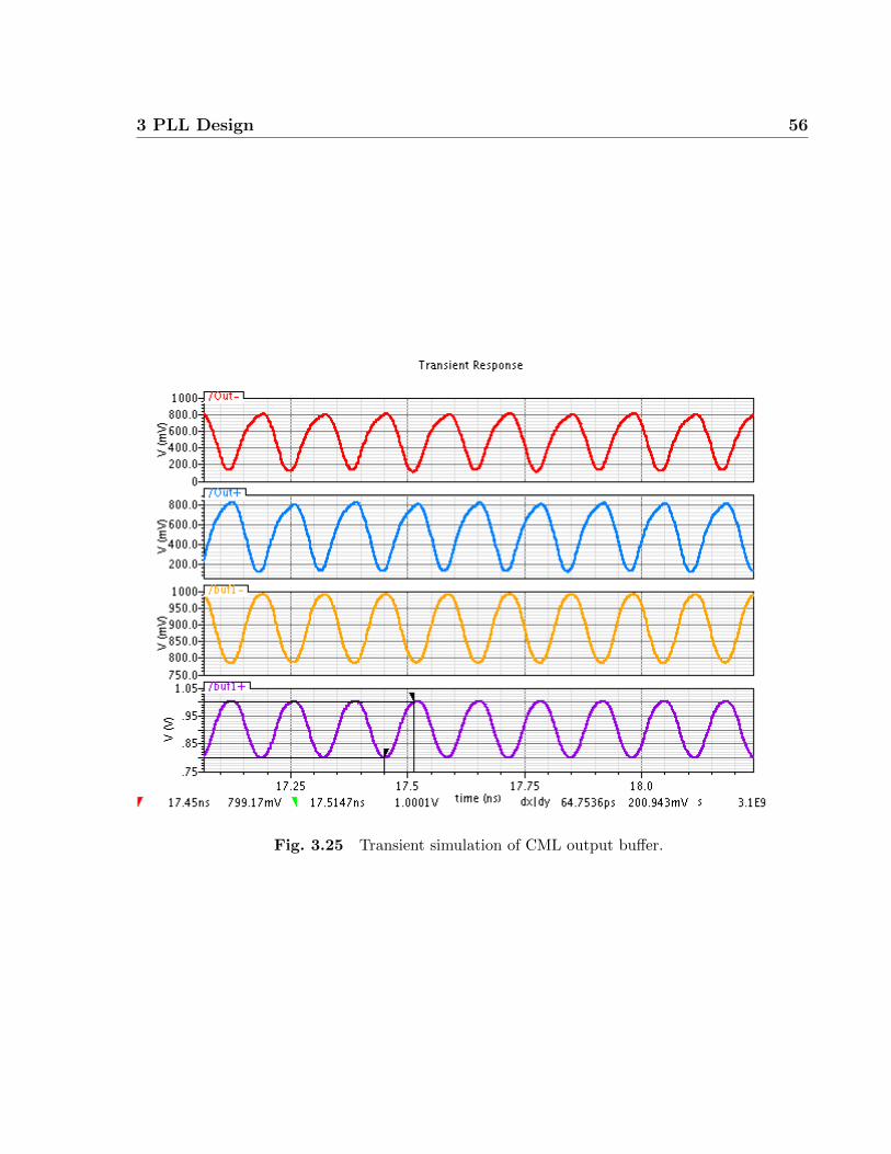
The operation of the input level shifter (schematic in Figure 3.11) can be observed in Figure
3.24. An input clock of 660 MHz (the maximum expected operating frequency of a pattern
generator, described in a later section) at 3.3 V can be seen, with the output at 1.2 V. The
CML buffer transient simulation is shown in Figure 3.25, with the outputs loaded with 50
Ω resistors and 20 pF capacitors. The input is from the VCO (out+/- on figure). The
output (buf1+/-) swing is approximately 200 mV, which can be observed from the delta
markers.
Fig. 3.24 Transient simulation of CMOS input level shifter.
3 PLL Design 56
Fig. 3.25 Transient simulation of CML output buffer.
3 PLL Design 57
3.3.7 PLL
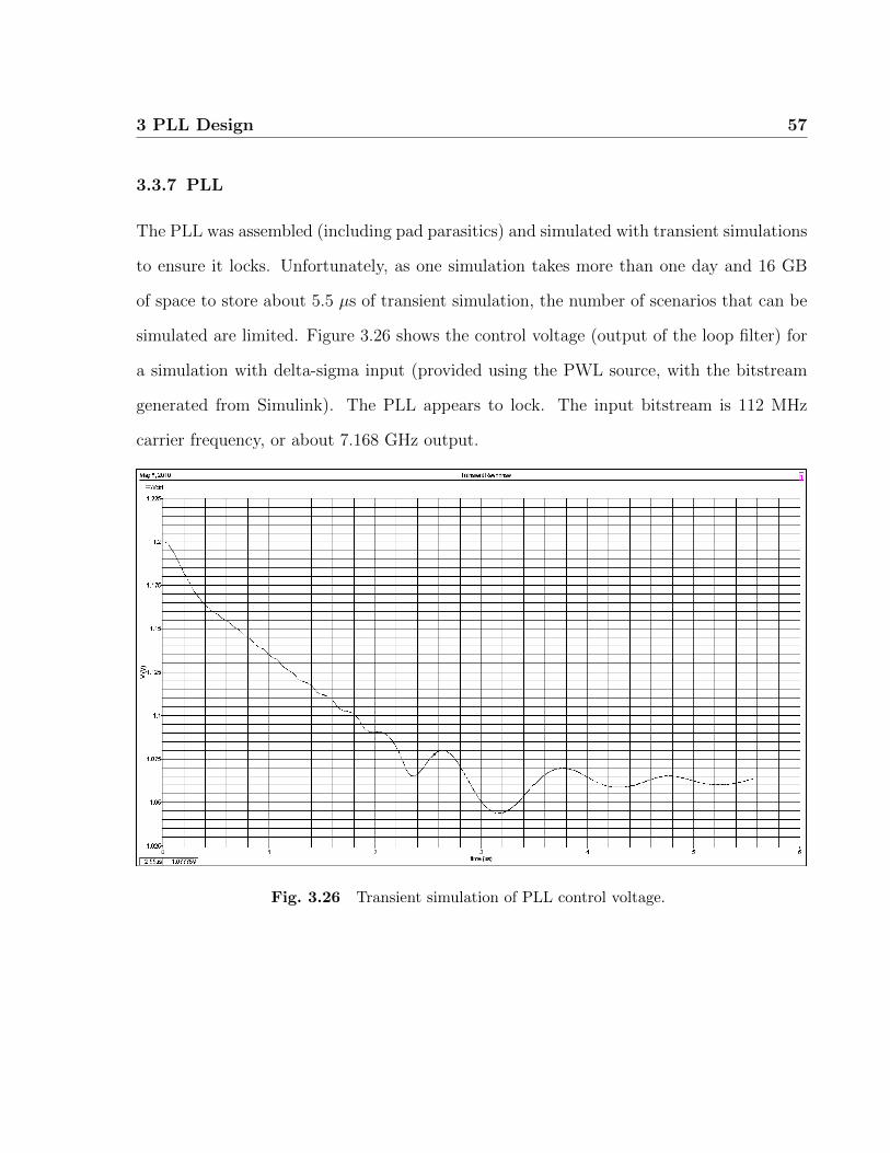
The PLL was assembled (including pad parasitics) and simulated with transient simulations
to ensure it locks. Unfortunately, as one simulation takes more than one day and 16 GB
of space to store about 5.5 µs of transient simulation, the number of scenarios that can be
simulated are limited. Figure 3.26 shows the control voltage (output of the loop filter) for
a simulation with delta-sigma input (provided using the PWL source, with the bitstream
generated from Simulink). The PLL appears to lock. The input bitstream is 112 MHz
carrier frequency, or about 7.168 GHz output.
Fig. 3.26 Transient simulation of PLL control voltage.
3 PLL Design 58
3.4 Summary
For testing frequency and phase synthesis at high speeds, a custom PLL was designed and
built in the IBM cmrf8sf 130 nm process (cmosp13) . A top-down design methodology was
employed to impose a desired phase transfer function. The transistor-level design of each
component (PFD, loop filter, VCO, frequency dividers, and input/output circuitry) of the
phase-locked loop was described, followed by the post-layout extracted simulation results
for each block and the entire PLL. The PLL is found to work as expected.
59
Chapter 4
PCB Design
In order to interface between the PLL to off-board equipment and instrumentation, a
printed-circuit board (PCB) must be designed and fabricated. As the PLL loop filter is
not on-chip, it must also be constructed on the PCB. Two sets of PCBs were designed; the
first to verify the functionality of the filter, and the second to accommodate the PLL and
all associated components. All PCBs were designed using Cadence Allegro.
4.1 Filter Test PCB
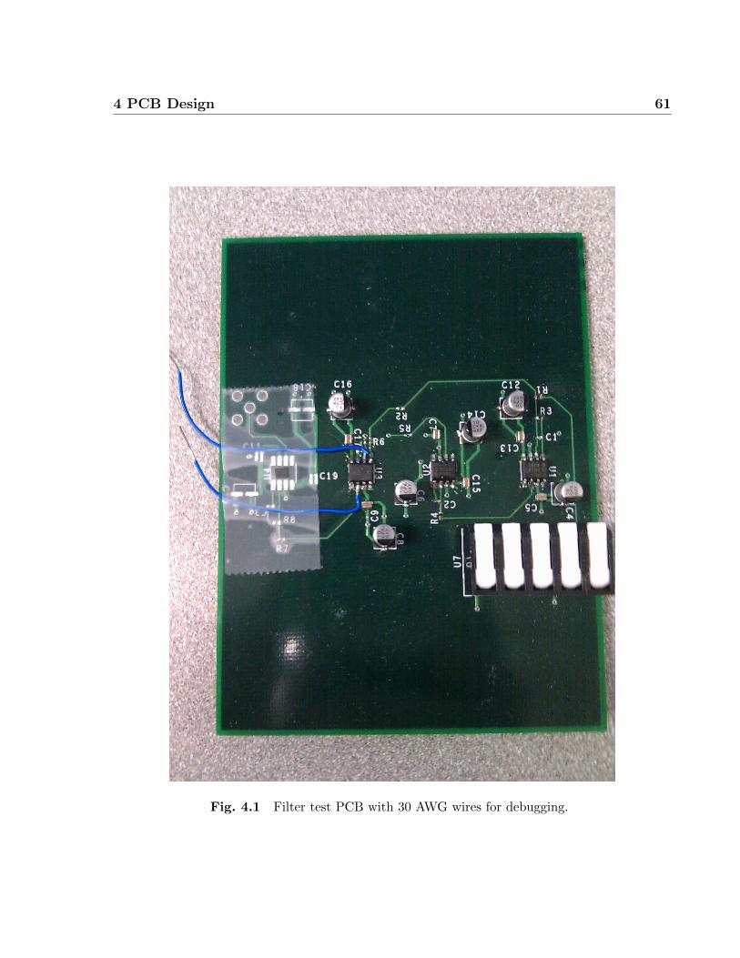
A four-layer PCB on standard FR4 substrate, shown in Figure 4.1, was built for testing the
loop filter. This PCB served to debug the library and footprints that were custom-built,
validate the selection of the AD8045 opamp, and to determine if any components need to
be changed or added. An FR4 substrate PCB is much less costly (approximately $250
versus $2000 for five PCBs) than one built on Rogers material, which would be required as
the PLL is operating at high frequencies. For this PCB, the SOIC (small-outline integrated
circuit) version of the AD8045 was used, as it allows for debugging via the soldering of small
4 PCB Design 60
gauge wires to bring out signals directly. This would usually not be an option for packages
smaller than SOIC, as the pins are either too small or they may lack pins altogether.
The filter test PCB contains a Tyco screwless terminal block for power and input con-
nections, and an SMA connector for output. It uses a 10 µF SMD electrolytic capacitors in
series with a low equivalent series inductance (ESL) reverse-geometry 0508 0.1 µF capaci-
tor per rail per opamp for power supply decoupling. This is recommended by the AD8045
datasheet. The stackup of the PCB consists of two signal layers (top and bottom), with
a split power plane (VDD and VSS, + and - 5 V respectively) and a ground plane. The
analog ground does not have its own plane.
With the initial run of the filter test PCB, it was discovered the footprint for the
opamp was incorrect, and unfortunately the PCBs had to be scrapped and manufactured
again. Using the boards from the second run, it was discovered that analog ground needed
decoupling as well, which was not mentioned in the datasheet. This was provided by
inserting a through-hole 0.1 µF capacitor into the screwless terminal block between the
analog ground and ground terminals as a temporary measure. The gain of the Tow-Thomas
filter was then verified by varying the frequency of the input signal from a function generator
(Agilent 33250A). The last stage could not be reliably tested in open-loop, as it contains a
pole at DC.
4 PCB Design 61
Fig. 4.1 Filter test PCB with 30 AWG wires for debugging.
4 PCB Design 62
4.2 Chip-Bonded PCB
The final iteration of the PCB is intended to host the PLL die as well as the loop filter. It
incorporates the improvements ascertained to be needed from the filter test PCB, as well
as design features which aid in high-speed operation.
4.2.1 Grounding and Stackup
As recommended in [31], a split analog/digital ground plane is not used. With split ground
planes, it is likely that a trace will need to cross the gap. If it does, the return current
may have to take a large loop to return to ground, as the most direct path (underneath the
trace) is not contiguous. This would create a large inductance. Instead, the ground plane
is isolated into analog and digital sections, and is connected together at one location only
(underneath the PLL die). This satisfies the condition that the digital and analog grounds
need to be tied together at some point (as they are not on-chip) for the same reference
point with a low impedance connection. Having the common-ground connection being
established at the power supply would be higher impedance in the power path, creating
a higher noise voltage (and more coupling) between the two planes when current flows
to ground. Additionally, great care is taken not to route any traces over the gaps in the
planes. This helps ensure the return current for the digital power supply does not cross
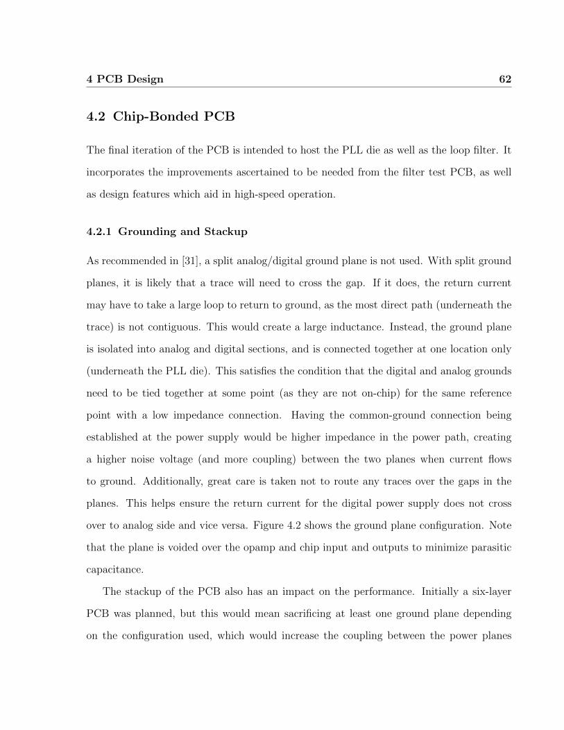
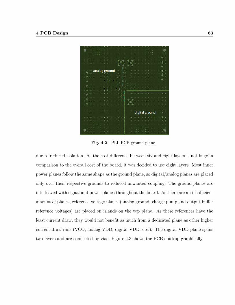
over to analog side and vice versa. Figure 4.2 shows the ground plane configuration. Note
that the plane is voided over the opamp and chip input and outputs to minimize parasitic
capacitance.
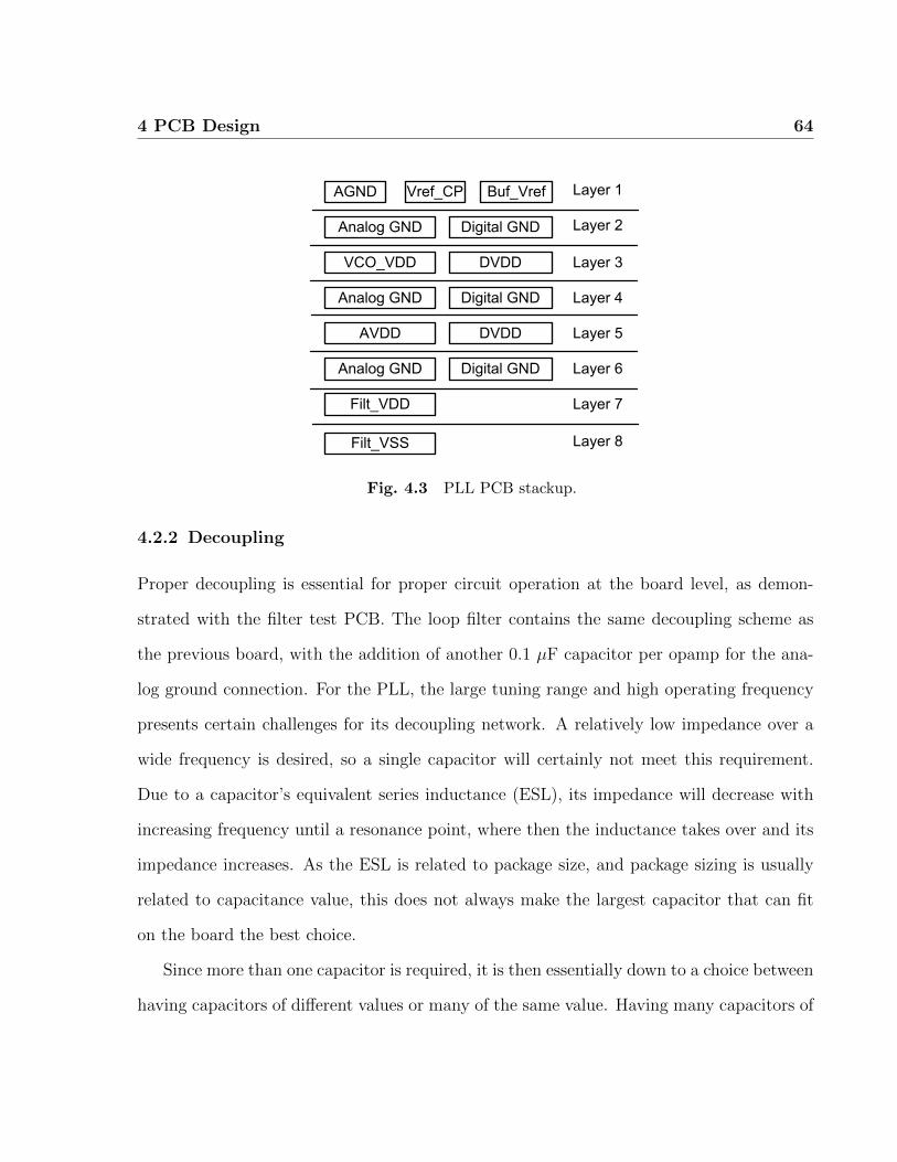
The stackup of the PCB also has an impact on the performance. Initially a six-layer
PCB was planned, but this would mean sacrificing at least one ground plane depending
on the configuration used, which would increase the coupling between the power planes
4 PCB Design 63
Fig. 4.2 PLL PCB ground plane.
due to reduced isolation. As the cost difference between six and eight layers is not huge in
comparison to the overall cost of the board, it was decided to use eight layers. Most inner
power planes follow the same shape as the ground plane, so digital/analog planes are placed
only over their respective grounds to reduced unwanted coupling. The ground planes are
interleaved with signal and power planes throughout the board. As there are an insufficient
amount of planes, reference voltage planes (analog ground, charge pump and output buffer
reference voltages) are placed on islands on the top plane. As these references have the
least current draw, they would not benefit as much from a dedicated plane as other higher
current draw rails (VCO, analog VDD, digital VDD, etc.). The digital VDD plane spans
two layers and are connected by vias. Figure 4.3 shows the PCB stackup graphically.
4 PCB Design 64
AGND Buf_VrefVref_CP
Digital GNDAnalog GND
DVDDVCO_VDD
Digital GNDAnalog GND
DVDDAVDD
Filt_VDD
Filt_VSS
Layer 1
Layer 8
Layer 2
Layer 3
Layer 4
Layer 5
Layer 7
Digital GNDAnalog GND Layer 6
Fig. 4.3 PLL PCB stackup.
4.2.2 Decoupling
Proper decoupling is essential for proper circuit operation at the board level, as demon-
strated with the filter test PCB. The loop filter contains the same decoupling scheme as
the previous board, with the addition of another 0.1 µF capacitor per opamp for the ana-
log ground connection. For the PLL, the large tuning range and high operating frequency
presents certain challenges for its decoupling network. A relatively low impedance over a
wide frequency is desired, so a single capacitor will certainly not meet this requirement.
Due to a capacitor’s equivalent series inductance (ESL), its impedance will decrease with
increasing frequency until a resonance point, where then the inductance takes over and its
impedance increases. As the ESL is related to package size, and package sizing is usually
related to capacitance value, this does not always make the largest capacitor that can fit
on the board the best choice.
Since more than one capacitor is required, it is then essentially down to a choice between
having capacitors of different values or many of the same value. Having many capacitors of
4 PCB Design 65
different values will allow the impedance to be lowered across a frequency range. However,
the ESL of each capacitor will cause anti-resonance spikes [32], making the impedance higher
and the decoupling network less effective at certain frequencies. This can be overcome by
placing the capacitances (and poles) relatively closely together, which would reduce the
effects of the anti-resonance [33]. Another option is to place many capacitors of the same
value in parallel. The capacitance would increase while the inductance would decrease,
which would widen the low impedance region of the decoupling network [31]. It also avoids
the problem of anti-resonance spikes. This method is referred to the “big V” method in
[33], and is used here because of its simplicity in both design and sourcing of parts.
To start designing with the “big V” method, a capacitor package is first chosen. The
0306 reverse-geometry package was chosen for its low ESL and small footprint. The largest
capacitance with the package available was then used, as the larger capacitance allows the
capacitor self-resonance to be at a higher frequency as the ESL is the same for all capacitors
with the same package. The Murata LLM series 220 nF capacitor was used; the datasheet
specifies an ESL of 116 pF. The decoupling network was then simulated in Spectre and the
number of capacitors increased until the impedance over the range of working frequencies
appear satisfactory. Eight capacitors were used per rail. The impedance of each network
was obtained from AC simulations and can be seen in Figure 4.4. The network impedance
remains below 1 Ω from approximately 90 kHz to 10 GHz.
4.2.3 Input/Output
The input and output of the PCB are equipped with SMA connectors. The input is
terminated with a 50 Ω resistor. The high-speed differential outputs, however, needed a
transmission line to be correctly terminated at high frequencies. Striplines and microstrips
were considered; microstrips were chosen because striplines would be very difficult to debug
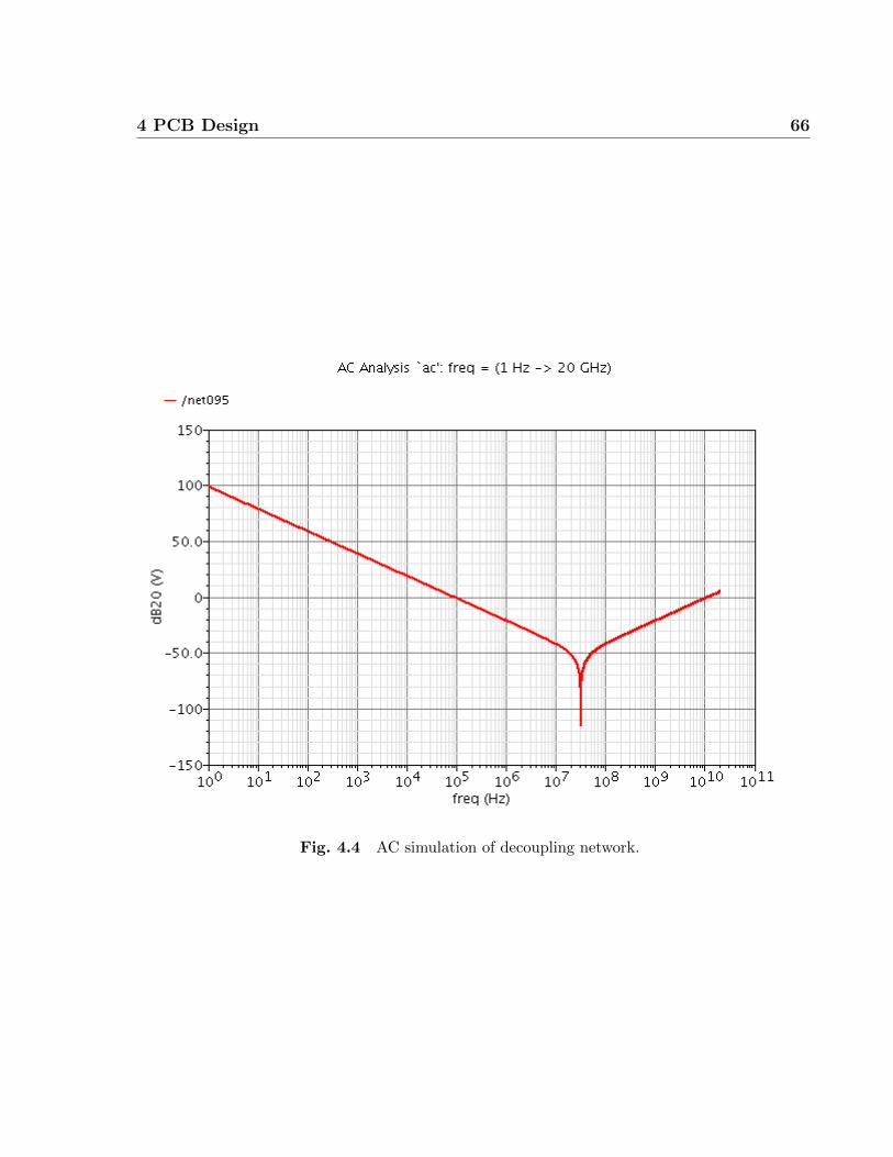
4 PCB Design 66
Fig. 4.4 AC simulation of decoupling network.
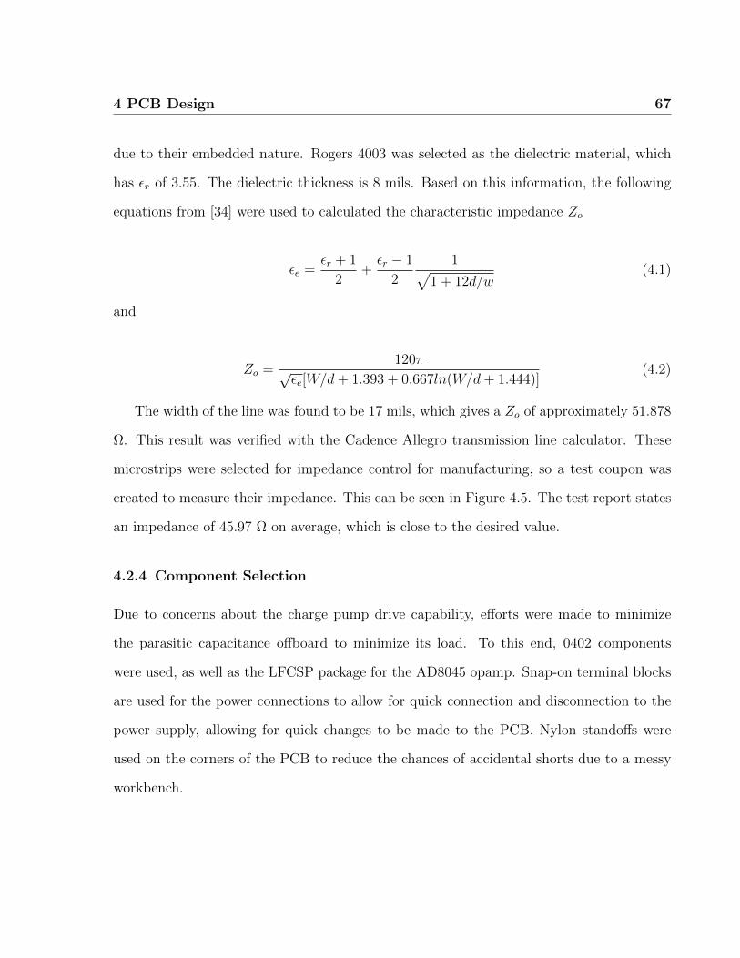
4 PCB Design 67
due to their embedded nature. Rogers 4003 was selected as the dielectric material, which
has εr of 3.55. The dielectric thickness is 8 mils. Based on this information, the following
equations from [34] were used to calculated the characteristic impedance Zo
εe =εr + 1
2+εr − 1
2
1√1 + 12d/w
(4.1)
and
Zo =120π
√εe[W/d+ 1.393 + 0.667ln(W/d+ 1.444)]
(4.2)
The width of the line was found to be 17 mils, which gives a Zo of approximately 51.878
Ω. This result was verified with the Cadence Allegro transmission line calculator. These
microstrips were selected for impedance control for manufacturing, so a test coupon was
created to measure their impedance. This can be seen in Figure 4.5. The test report states
an impedance of 45.97 Ω on average, which is close to the desired value.
4.2.4 Component Selection
Due to concerns about the charge pump drive capability, efforts were made to minimize
the parasitic capacitance offboard to minimize its load. To this end, 0402 components
were used, as well as the LFCSP package for the AD8045 opamp. Snap-on terminal blocks
are used for the power connections to allow for quick connection and disconnection to the
power supply, allowing for quick changes to be made to the PCB. Nylon standoffs were
used on the corners of the PCB to reduce the chances of accidental shorts due to a messy
workbench.
4 PCB Design 68
Fig. 4.5 Microstrip test coupon.
4 PCB Design 69
4.2.5 Die Bonding
Normally, the die would be bonded to a package with pins using bondwires. This is included
as part of CMC’s fabrication service. However, according to [35], none of the standard
packages offered by CMC are rated for operation above 2 GHz. Flip-chip ball grid array
(BGA)-type packaging would be ideal as it has no bondwires, but it is very expensive
(about $5000), which is above chip fabrication cost. Therefore, it was decided to bond the
die to the PCB itself. This would eliminate the additional parasitics of a package. This
process is often referred to as COB (chip-on-board).
There are various factors to consider when bonding a die to a PCB. Each bonding house
has different requirements as to what their machinery can accommodate. The most obvious
restriction is perhaps the footprint. It is advantageous to minimize the pad size to reduce
parasitic capacitance, but there are minimum size requirements to be obeyed. There are also
certain surface finishes that are required; many houses require soft bondable gold, which is
one of the most costly finishing options. Some require ENIG (Electroless Nickel Immersion
Gold) only, which is more expensive than standard HASL (Hot Air Solder Levelling), but is
becoming more popular because it is RoHS (Reduction of Hazardous Substances) compliant.
ENIG is less expensive than soft bondable gold, making it more attractive. Component
clearance is also an issue; both the height of nearby parts and their distance from the
bonding pads must be taken into account to ensure accessibility. There is usually also a
maximum bondwire length restriction, requiring careful footprint design. Finally, it has to
be decided whether the die should be encapsulated in epoxy, which protects the chip but
also hinders its removal in the future if required.
After research and with the assistance of CMC, AIT Technology was chosen for die
bonding. They require only ENIG finish, and had the lowest cost per die bonded. The dies
4 PCB Design 70
were encapsulated in epoxy. The PCBs were shipped directly from the fabrication house
to AIT to minimize the chances of contaminating the finish.
4.2.6 Fabrication
Initially, the PCB was designed with blind vias. Blind vias are preferable because they lack
the stub present with traditional vias, which can cause unwanted reflections and present
additional parasitics. This caused many issues when trying to find a PCB fabrication house,
because of the number of layers required. To build a board with blind vias, each layer must
be drilled separately and laminated together. This means the precision of the drill must be
extremely high, and the chance of error is compounded with each additional layer. Due to
the nature of the stackup, a set of blind vias must go from the top layer to almost every
single layer. Eventually, the blind via PCB was abandoned, and backdrilled vias were
investigated. Backdriled vias are traditional vias with the back drilled out with a slightly
larger drill, also eliminating the unwanted stub. However, it proved very difficult to find
a fabrication house willing to do backdrilling for a reasonable price; therefore, traditional
vias were used. The final board, manufactured by Sierra Proto, with bonded die can be
seen in Figures 4.6 and 4.7. The bonded die is marked with a white box in Figure 4.6.
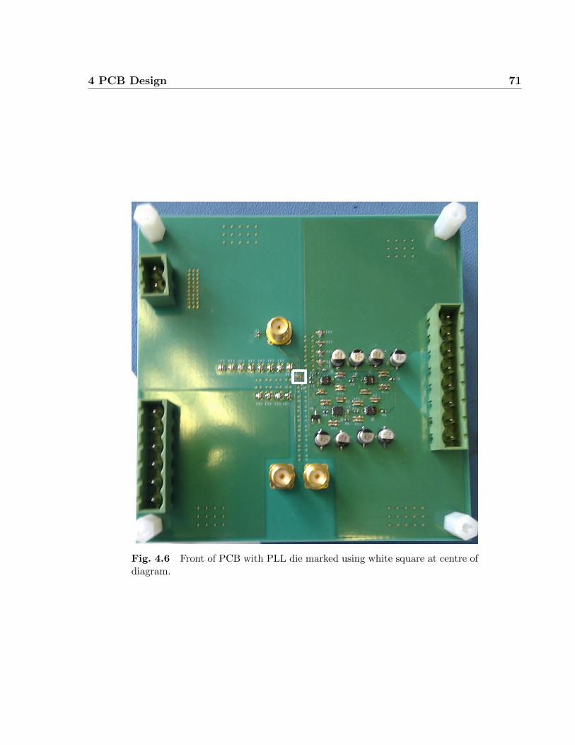
4 PCB Design 71
Fig. 4.6 Front of PCB with PLL die marked using white square at centre ofdiagram.
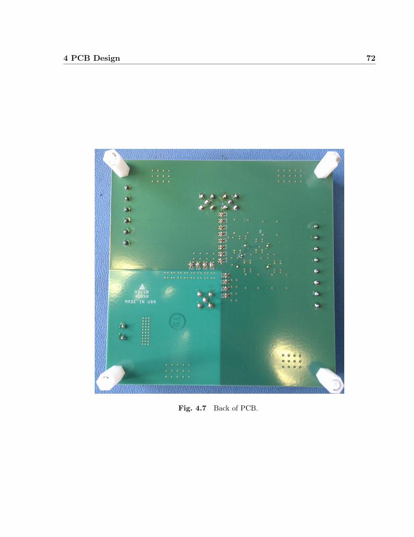
4 PCB Design 72
Fig. 4.7 Back of PCB.
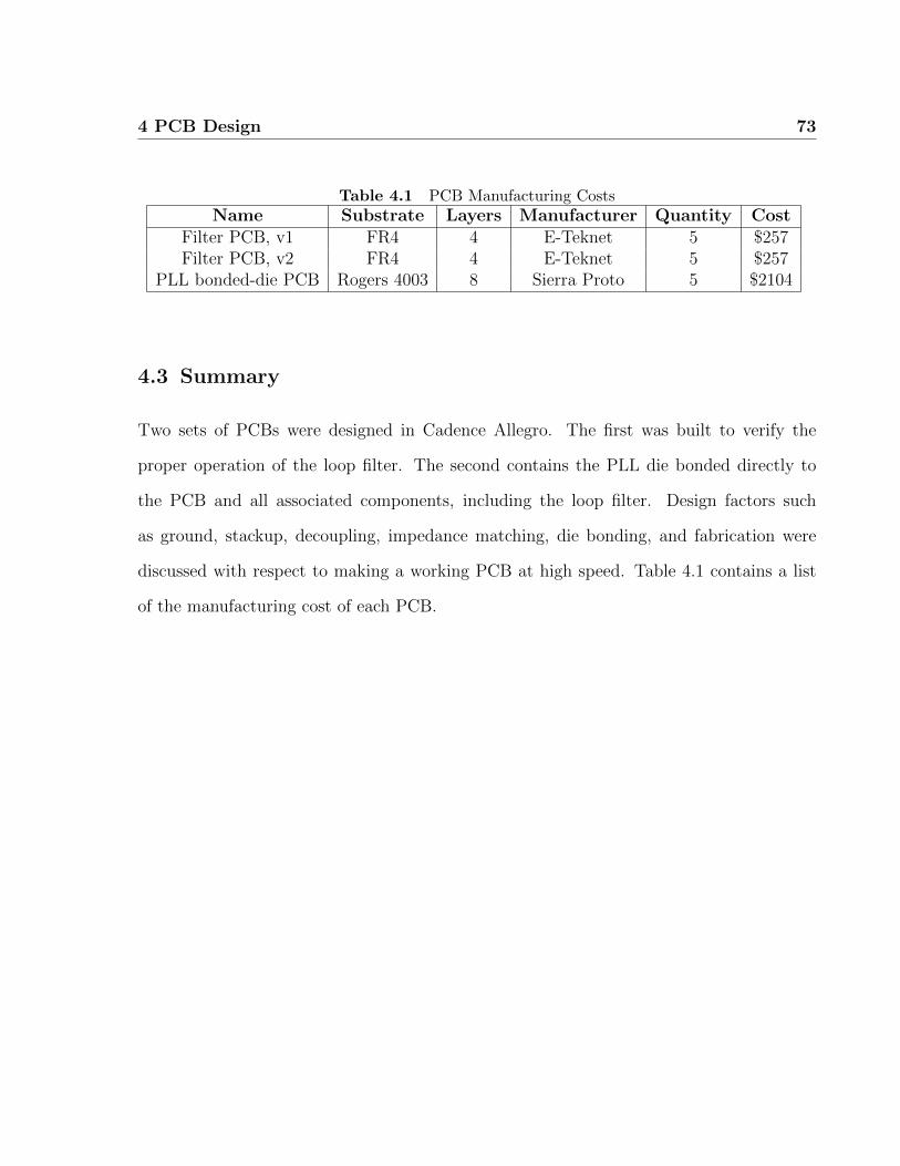
4 PCB Design 73
Table 4.1 PCB Manufacturing CostsName Substrate Layers Manufacturer Quantity Cost
Filter PCB, v1 FR4 4 E-Teknet 5 $257Filter PCB, v2 FR4 4 E-Teknet 5 $257
PLL bonded-die PCB Rogers 4003 8 Sierra Proto 5 $2104
4.3 Summary
Two sets of PCBs were designed in Cadence Allegro. The first was built to verify the
proper operation of the loop filter. The second contains the PLL die bonded directly to
the PCB and all associated components, including the loop filter. Design factors such
as ground, stackup, decoupling, impedance matching, die bonding, and fabrication were
discussed with respect to making a working PCB at high speed. Table 4.1 contains a list
of the manufacturing cost of each PCB.
74
Chapter 5
Experimental Results
Using the PCB with bonded PLL die, the functionality and performance of the phase and
frequency signal generation system is explored.
5.1 Test Setup
In order to implement the phase/frequency generation system, a register or some other
kind of memory is required. A delta-sigma bitstream is stored in this memory and looped
to create a continuous bitstream. On-chip, an existing IEEE 1149.1 bus can be utilized to
receive data from off-chip and store the data into a register that is routed to the components
under test. A phase-locked loop is then used as an anti-imaging filter as well as provides a
means of scaling up the output frequency. Figure 5.1 shows the way the system is repre-
sented by the test setup. The delta-sigma modulator and the DFC/DTC are implemented
in software, and the resultant output is looped to create an uninterrupted, continuous bit-
stream. As this is identical to the simulation setup, the bits are saved from Matlab and
loaded into a Hewlett Packard 81130A pattern generator. It is programmed over GPIB via
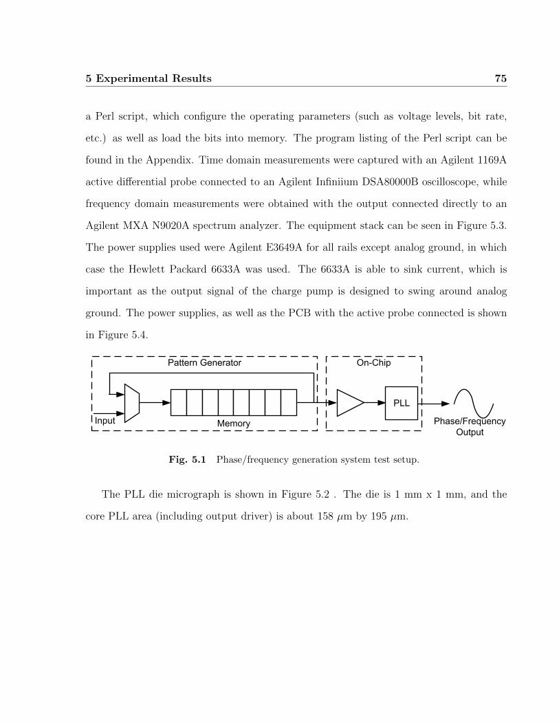
5 Experimental Results 75
a Perl script, which configure the operating parameters (such as voltage levels, bit rate,
etc.) as well as load the bits into memory. The program listing of the Perl script can be
found in the Appendix. Time domain measurements were captured with an Agilent 1169A
active differential probe connected to an Agilent Infiniium DSA80000B oscilloscope, while
frequency domain measurements were obtained with the output connected directly to an
Agilent MXA N9020A spectrum analyzer. The equipment stack can be seen in Figure 5.3.
The power supplies used were Agilent E3649A for all rails except analog ground, in which
case the Hewlett Packard 6633A was used. The 6633A is able to sink current, which is
important as the output signal of the charge pump is designed to swing around analog
ground. The power supplies, as well as the PCB with the active probe connected is shown
in Figure 5.4.
Pattern Generator On-Chip
PLL
Memory Phase/Frequency
Output
Input
Fig. 5.1 Phase/frequency generation system test setup.
The PLL die micrograph is shown in Figure 5.2 . The die is 1 mm x 1 mm, and the
core PLL area (including output driver) is about 158 µm by 195 µm.
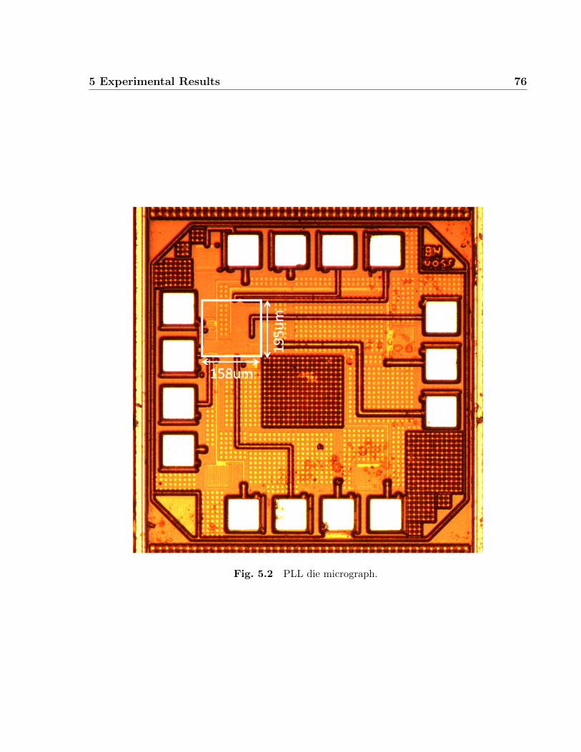
5 Experimental Results 76
Fig. 5.2 PLL die micrograph.
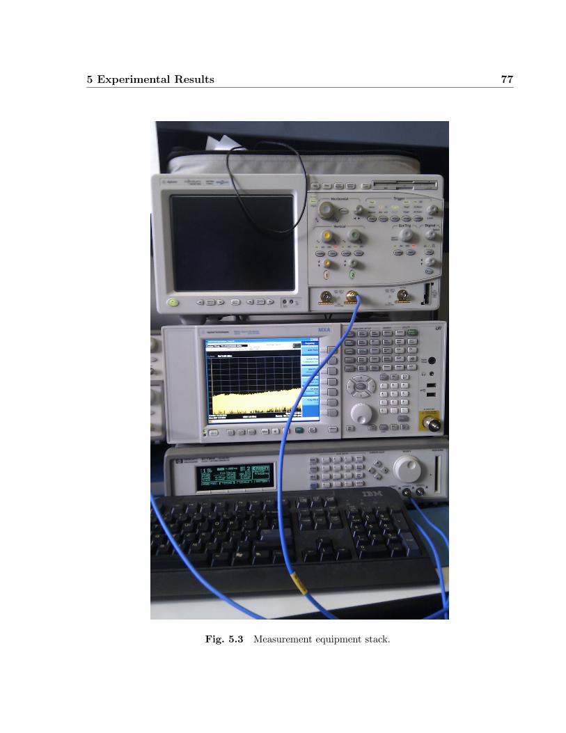
5 Experimental Results 77
Fig. 5.3 Measurement equipment stack.
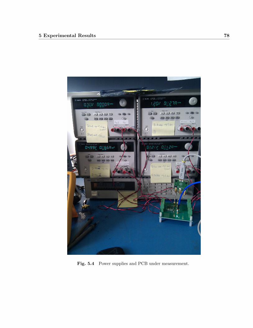
5 Experimental Results 78
Fig. 5.4 Power supplies and PCB under measurement.
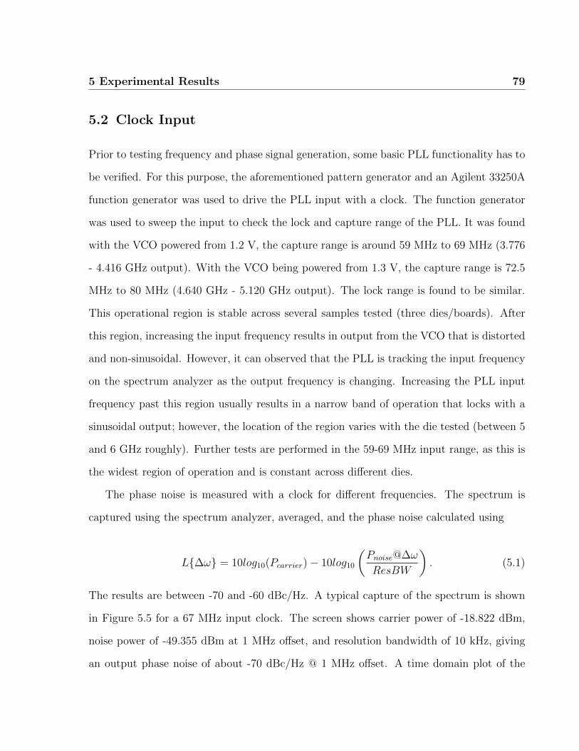
5 Experimental Results 79
5.2 Clock Input
Prior to testing frequency and phase signal generation, some basic PLL functionality has to
be verified. For this purpose, the aforementioned pattern generator and an Agilent 33250A
function generator was used to drive the PLL input with a clock. The function generator
was used to sweep the input to check the lock and capture range of the PLL. It was found
with the VCO powered from 1.2 V, the capture range is around 59 MHz to 69 MHz (3.776
- 4.416 GHz output). With the VCO being powered from 1.3 V, the capture range is 72.5
MHz to 80 MHz (4.640 GHz - 5.120 GHz output). The lock range is found to be similar.
This operational region is stable across several samples tested (three dies/boards). After
this region, increasing the input frequency results in output from the VCO that is distorted
and non-sinusoidal. However, it can observed that the PLL is tracking the input frequency
on the spectrum analyzer as the output frequency is changing. Increasing the PLL input
frequency past this region usually results in a narrow band of operation that locks with a
sinusoidal output; however, the location of the region varies with the die tested (between 5
and 6 GHz roughly). Further tests are performed in the 59-69 MHz input range, as this is
the widest region of operation and is constant across different dies.
The phase noise is measured with a clock for different frequencies. The spectrum is
captured using the spectrum analyzer, averaged, and the phase noise calculated using
L∆ω = 10log10(Pcarrier)− 10log10
(Pnoise@∆ω
ResBW
). (5.1)
The results are between -70 and -60 dBc/Hz. A typical capture of the spectrum is shown
in Figure 5.5 for a 67 MHz input clock. The screen shows carrier power of -18.822 dBm,
noise power of -49.355 dBm at 1 MHz offset, and resolution bandwidth of 10 kHz, giving
an output phase noise of about -70 dBc/Hz @ 1 MHz offset. A time domain plot of the
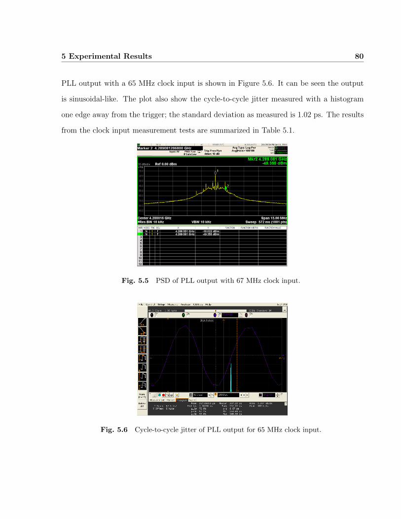
5 Experimental Results 80
PLL output with a 65 MHz clock input is shown in Figure 5.6. It can be seen the output
is sinusoidal-like. The plot also show the cycle-to-cycle jitter measured with a histogram
one edge away from the trigger; the standard deviation as measured is 1.02 ps. The results
from the clock input measurement tests are summarized in Table 5.1.
Fig. 5.5 PSD of PLL output with 67 MHz clock input.
Fig. 5.6 Cycle-to-cycle jitter of PLL output for 65 MHz clock input.
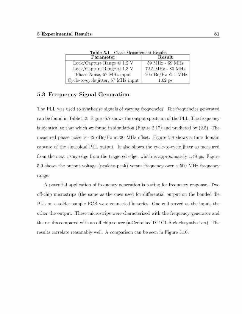
5 Experimental Results 81
Table 5.1 Clock Measurement ResultsParameter Result
Lock/Capture Range @ 1.2 V 59 MHz - 69 MHzLock/Capture Range @ 1.3 V 72.5 MHz - 80 MHzPhase Noise, 67 MHz input -70 dBc/Hz @ 1 MHz
Cycle-to-cycle jitter, 67 MHz input 1.02 ps
5.3 Frequency Signal Generation
The PLL was used to synthesize signals of varying frequencies. The frequencies generated
can be found in Table 5.2. Figure 5.7 shows the output spectrum of the PLL. The frequency
is identical to that which we found in simulation (Figure 2.17) and predicted by (2.5). The
measured phase noise is -42 dBc/Hz at 20 MHz offset. Figure 5.8 shows a time domain
capture of the sinusoidal PLL output. It also shows the cycle-to-cycle jitter as measured
from the next rising edge from the triggered edge, which is approximately 1.48 ps. Figure
5.9 shows the output voltage (peak-to-peak) versus frequency over a 500 MHz frequency
range.
A potential application of frequency generation is testing for frequency response. Two
off-chip microstrips (the same as the ones used for differential output on the bonded die
PLL on a solder sample PCB were connected in series. One end served as the input, the
other the output. These microstrips were characterized with the frequency generator and
the results compared with an off-chip source (a Centellax TG1C1-A clock synthesizer). The
results correlate reasonably well. A comparison can be seen in Figure 5.10.
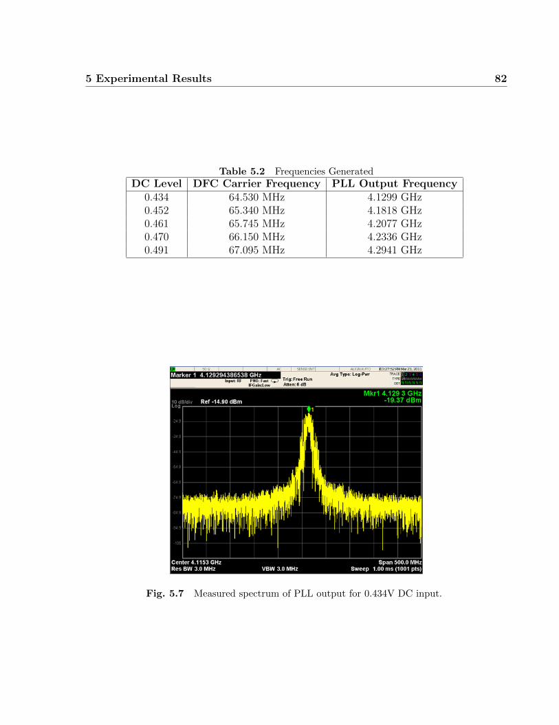
5 Experimental Results 82
Table 5.2 Frequencies GeneratedDC Level DFC Carrier Frequency PLL Output Frequency
0.434 64.530 MHz 4.1299 GHz0.452 65.340 MHz 4.1818 GHz0.461 65.745 MHz 4.2077 GHz0.470 66.150 MHz 4.2336 GHz0.491 67.095 MHz 4.2941 GHz
Fig. 5.7 Measured spectrum of PLL output for 0.434V DC input.
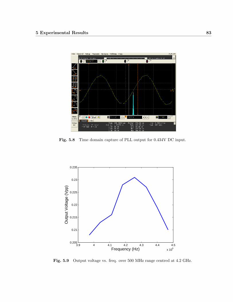
5 Experimental Results 83
Fig. 5.8 Time domain capture of PLL output for 0.434V DC input.
3.9 4 4.1 4.2 4.3 4.4 4.5
x 109
0.205
0.21
0.215
0.22
0.225
0.23
0.235
Frequency (Hz)
Out
put V
olta
ge (
Vpp
)
Fig. 5.9 Output voltage vs. freq. over 500 MHz range centred at 4.2 GHz.
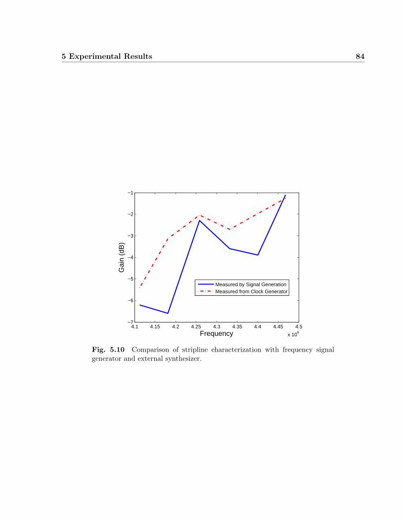
5 Experimental Results 84
4.1 4.15 4.2 4.25 4.3 4.35 4.4 4.45 4.5
x 109
−7
−6
−5
−4
−3
−2
−1
Frequency
Gai
n (d
B)
Measured by Signal GenerationMeasured from Clock Generator
Fig. 5.10 Comparison of stripline characterization with frequency signalgenerator and external synthesizer.
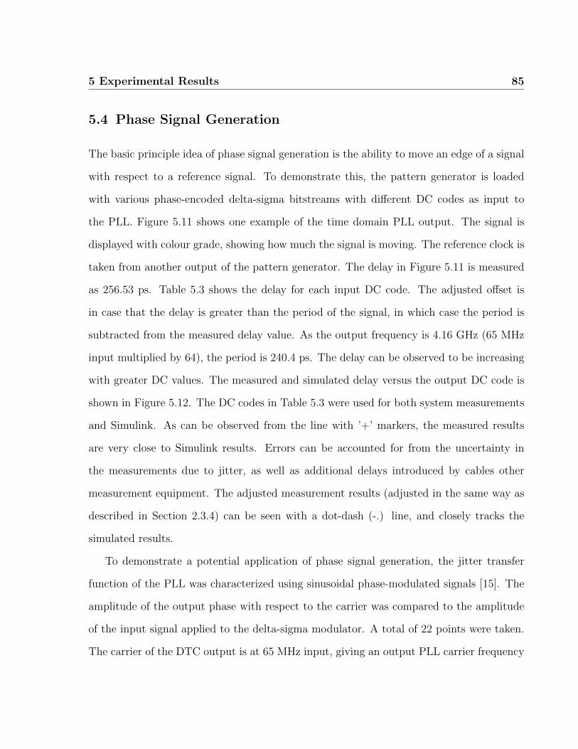
5 Experimental Results 85
5.4 Phase Signal Generation
The basic principle idea of phase signal generation is the ability to move an edge of a signal
with respect to a reference signal. To demonstrate this, the pattern generator is loaded
with various phase-encoded delta-sigma bitstreams with different DC codes as input to
the PLL. Figure 5.11 shows one example of the time domain PLL output. The signal is
displayed with colour grade, showing how much the signal is moving. The reference clock is
taken from another output of the pattern generator. The delay in Figure 5.11 is measured
as 256.53 ps. Table 5.3 shows the delay for each input DC code. The adjusted offset is
in case that the delay is greater than the period of the signal, in which case the period is
subtracted from the measured delay value. As the output frequency is 4.16 GHz (65 MHz
input multiplied by 64), the period is 240.4 ps. The delay can be observed to be increasing
with greater DC values. The measured and simulated delay versus the output DC code is
shown in Figure 5.12. The DC codes in Table 5.3 were used for both system measurements
and Simulink. As can be observed from the line with ’+’ markers, the measured results
are very close to Simulink results. Errors can be accounted for from the uncertainty in
the measurements due to jitter, as well as additional delays introduced by cables other
measurement equipment. The adjusted measurement results (adjusted in the same way as
described in Section 2.3.4) can be seen with a dot-dash (-.) line, and closely tracks the
simulated results.
To demonstrate a potential application of phase signal generation, the jitter transfer
function of the PLL was characterized using sinusoidal phase-modulated signals [15]. The
amplitude of the output phase with respect to the carrier was compared to the amplitude
of the input signal applied to the delta-sigma modulator. A total of 22 points were taken.
The carrier of the DTC output is at 65 MHz input, giving an output PLL carrier frequency
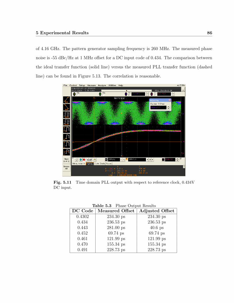
5 Experimental Results 86
of 4.16 GHz. The pattern generator sampling frequency is 260 MHz. The measured phase
noise is -55 dBc/Hz at 1 MHz offset for a DC input code of 0.434. The comparison between
the ideal transfer function (solid line) versus the measured PLL transfer function (dashed
line) can be found in Figure 5.13. The correlation is reasonable.
Fig. 5.11 Time domain PLL output with respect to reference clock, 0.434VDC input.
Table 5.3 Phase Output ResultsDC Code Measured Offset Adjusted Offset
0.4302 234.30 ps 234.30 ps0.434 236.53 ps 236.53 ps0.443 281.00 ps 40.6 ps0.452 69.74 ps 69.74 ps0.461 121.99 ps 121.99 ps0.470 155.34 ps 155.34 ps0.491 228.73 ps 228.73 ps
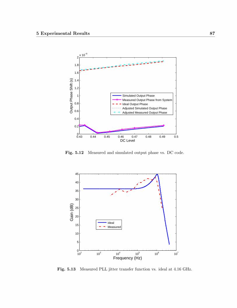
5 Experimental Results 87
0.43 0.44 0.45 0.46 0.47 0.48 0.49 0.50
0.2
0.4
0.6
0.8
1
1.2
1.4
1.6
1.8
2x 10⁻⁹
DC Level
Out
put P
hase
Shi
ft (s
)
Simulated Output PhaseMeasured Output Phase from SystemIdeal Output PhaseAdjusted Simulated Output PhaseAdjusted Measured Output Phase
Fig. 5.12 Measured and simulated output phase vs. DC code.
102 103 104 105 106 1070
5
10
15
20
25
30
35
40
45
Frequency (Hz)
Gai
n (d
B)
IdealMeasured
Fig. 5.13 Measured PLL jitter transfer function vs. ideal at 4.16 GHz.
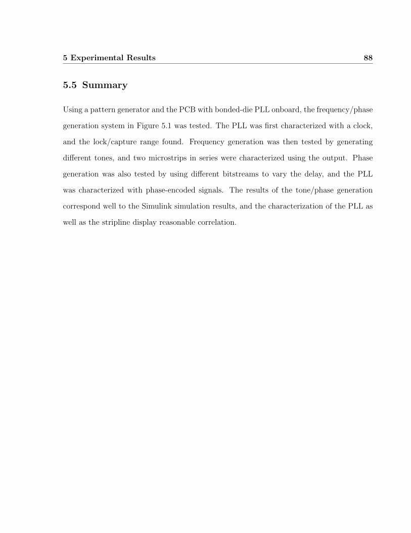
5 Experimental Results 88
5.5 Summary
Using a pattern generator and the PCB with bonded-die PLL onboard, the frequency/phase
generation system in Figure 5.1 was tested. The PLL was first characterized with a clock,
and the lock/capture range found. Frequency generation was then tested by generating
different tones, and two microstrips in series were characterized using the output. Phase
generation was also tested by using different bitstreams to vary the delay, and the PLL
was characterized with phase-encoded signals. The results of the tone/phase generation
correspond well to the Simulink simulation results, and the characterization of the PLL as
well as the stripline display reasonable correlation.

89
Chapter 6
Conclusions
6.1 Thesis Contributions
A phase/frequency signal generator for high-frequency applications amenable to digital
testing methodologies without additional test pins was presented. The system consists of
a software-based delta-sigma modulator and digital-to-frequency/digital-to-time converter,
followed by an on-chip phase-locked loop, discussed in Chapter 2. The delta-sigma modu-
lator and DTC/DFC were implemented in Matlab/Simulink and the system is verified to
behave as expected. A custom designed high-speed PLL is discussed in Chapter 3. The
PLL was first designed and simulated in Matlab using the high-order design methodology,
then implemented at the transistor level in Cadence Design Environment using IBM 130 nm
process. Simulations were then performed to ensure each subsystem performs as designed
and that the PLL locks. In Chapter 4, the design of a PCB that contains the PLL bonded
directly to the die and the with the lopo filter onboard is described. In Chapter 5, Using
a pattern generator as the circulating memory element, the signal generation system was
tested. Frequency signal generation was demonstrated using two microstrips connected
6 Conclusions 90
in series, while the PLL jitter transfer function was obtained using phase signal genera-
tion. Simulation and experimental results largely corroborate each other. As the testing
shows, although phase noise performance is much less than a fractional-N synthesizer, it
is nevertheless useful for various debug and diagnosis situations for the designer and test
engineer.
6.2 Future Work
For future work, the phase noise of the PLL could be improved in a future spin. For
individual components, the VCO and charge pump could use the most improvement, as
the phase noise of the VCO is not excellent and the charge pump current should be adjusted
to allow for greater drive capability. It might also be a useful demonstration to implement
the entire IEEE 1149.1 bus on-chip with the PLL and delta-sigma register.
In terms of applications, phase/frequency generation has other possibilities. For ex-
ample, if a mixer is implemented, a double-push type oscillator could be built since the
adjustable phase would allow for fine-tuning of each input, as phase mismatch is undesir-
able.
91
Appendix A
Perl Script for Pattern Generator
#!/usr/bin/perl
use strict;
use Lab::Instrument;
open (BIT_IN, ’<’, ’phase_0_442v_dc.txt’) or die $!;
my $pulse_gen = new Lab::Instrument(0,10); #GPIB board 0, addr 10
#print $pulse_gen->Query(’*IDN?’);
$pulse_gen -> Write(’*RST’); #Reset pulse generator
$pulse_gen -> Write(’:DISP OFF’); #Turn off display to increase prog. speed
$pulse_gen -> Write(’:OUTP1 OFF’); # Turn outputs off
$pulse_gen -> Write(’:OUTP2 OFF’);
$pulse_gen -> Write(’:FREQ 248MHz’); #Set output freq. 350 MHz
$pulse_gen -> Write(’:VOLT1:HIGH 1.2V’); #Set output voltage to 3.3V (into 50 ohms)
$pulse_gen -> Write(’:VOLT1:LOW 0V’);
$pulse_gen -> Write(’:DIG:SIGN:FORM NRZ’); #Set NRZ
$pulse_gen -> Write(’:ARM:SOUR IMM’); #Set continuous mode
$pulse_gen -> Write(’:DIG:PATT:STAT ON’); #Enable pattern mode
#Set segment 1 length (others are 0 from *RST)
#$pulse_gen -> Write(’:DIG:PATT:SEGM1:LENG 32768’);
#$pulse_gen -> Write(’:DIG:PATT:SEGM1:DATA1 #010101010101010101010101010101010’);
#$pulse_gen -> Write(’:DIG:PATT:SEGM1:LENG 32’);
#Read in bits and format
my $bitstream = join(’’, split(/,/, <BIT_IN>));
chomp $bitstream; #Chop off newline char at end
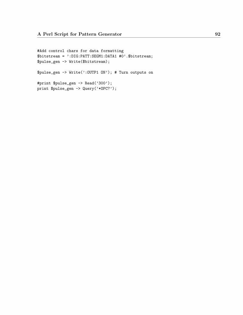
A Perl Script for Pattern Generator 92
#Add control chars for data formatting
$bitstream = ’:DIG:PATT:SEGM1:DATA1 #0’.$bitstream;
$pulse_gen -> Write($bitstream);
$pulse_gen -> Write(’:OUTP1 ON’); # Turn outputs on
#print $pulse_gen -> Read(’300’);
print $pulse_gen -> Query(’*OPC?’);
93
References
[1] M. M. Hafed and G. W. Roberts, “A 5-channel, variable resolution, 1o-ghz sampling
rate coherent tester/scilloscope IC and associated test vehicles,” in Proceedings of the
IEEE 2003 Custom Integrated Circuits Conference, pp. 621–624, 2003.
[2] K. P. Parker, The Boundary-Scan Handbook, Second Edition. Kluwer Academic Pub-
lishers, 1998.
[3] B. D. Muer and M. Steyaert, CMOS Fractional-N Synthesizers. Kluwer Academic
Publishers, 2003.
[4] W. Wang and H. C. Luong, “A 0.8-V 4.9-mW 1.2-GHz CMOS fractional-N frequency
synthesizer for UHF RFID reader,” IEEE Transactions on Circuits and Systems – I:
Regular Papers, vol. 55, pp. 2505–2513, Oct. 2008.
[5] S. Pellerano, S. Levantino, C. Samori, and A. L. Lacaita, “A 13.5-mW 5-GHz frequency
synthesizer with dynamic-logic frequency divider,” IEEE Journal of Solid State Cir-
cuits, vol. 39, pp. 378–383, Feb. 2004.
[6] C.-Y. Yang, C.-H. Chang, J.-H. Weng, and H.-M. Wu, “A 0.5/0.8-V 9-GHz frequency
synthesizer with doubling generation in 0.13-µm CMOS,” IEEE Transactions on Cir-
cuits and Systems – II: Express Briefs, vol. 58, pp. 65–69, Feb. 2011.
References 94
[7] P.-Y. Deng and J.-F. Kiang, “A 5-GHz CMOS frequency synthesizer with an injection-
locked frequency divider and differential switched capacitor,” IEEE Transactions on
Circuits and Systems – I: Regular Papers, vol. 56, pp. 320–326, Feb. 2009.
[8] S.-Y. Y. amd Wei-Zen Chen and T.-Y. Lu, “A 7.1 mW, 10 GHz all digital frequency
synthesizer with dynamically reconın Agured digital loop filter in 90 nm CMOS tech-
nology,” IEEE Journal of Solid State Circuits, vol. 45, pp. 578–586, Mar. 2010.
[9] E. M. Hawrysh and G. W. Roberts, “An integration of memory-based analog signal
generation into current DFT architectures,” IEEE Transactions on Instrumentation
and Measurement, vol. 47, pp. 748–759, June 1998.
[10] S. Aouini and G. W. Roberts, “Generating test signals for noise-based NPR/ACPR
type tests in production,” in 2008 IEEE International Test Conference, Oct. 2008.
[11] G. W. Roberts, 304-634B Analog Singal Processing Course Notes. 2009.
[12] X. Haurie and G. W. Roberts, “A design, simulation and synthesis tool for delta-sigma-
modulator-based signal sources,” in 1996 IEEE International Symposium on Circuits
and Systems, vol. 4, (Atlanta, GA, USA), pp. 715–718, May 1996.
[13] S. Aouini and G. W. Roberts, “Frequency synthesis using digital-frequency conversion
and filtering,” Electronic Letters, vol. 46, pp. 979–980, July 2010.
[14] S. Aouini, Extending Test Signal Generation Using Sigma-Delta Encoding Beyond The
Voltage/Amplitude Domain. PhD thesis, McGill University, 2011.
[15] S. Aouini, K. Chuai, and G. W. Roberts, “A low-cost ATE phase signal generation
technique for test applications,” in 2010 IEEE International Test Conference, Jan.
2011.
References 95
[16] F. M. Gardner, Phaselock Techniques. John Wiley & Sons, Inc., 2005.
[17] Canadian Miroelectronics Corporation, “Fab: CMOSP13/IBM,” Feb. 2011.
https://www.cmc.ca/WhatWeOffer/Products/CMC-00001-43484.aspx; accessed
February 24, 2011.
[18] B. Razavi, Design of Analog CMOS Integrated Circuits. McGraw-Hill Education, 2001.
[19] W.-H. Lee, J.-D. Cho, and S.-D. Lee, “A high speed and low power phase-frequency
detector and charge-pump,” in Proc. of the Asia and South Pacific Design Automation
Conference, vol. 1, (Wanchai, Hong Kong), pp. 269–272, Jan. 1999.
[20] J. M. Rabaey, A. Chandrakasan, and B. Nikolic, Digital Integrated Circuits: A Design
Perspective. second ed.
[21] W. Rhee, “Design of high-performance CMOS charge pumps in phase-locked loops,”
in Proc. of the 1999 IEEE International Symposium on Circuits and Systems, vol. 2,
(Orlando, FL, USA), pp. 545–548, July 1999.
[22] C.-L. Ti, Y.-H. Liu, and T.-H. Lin, “A 2.4-GHz fractional-N PLL with a PFD/CP
linearization and an improved CP circuit,” in Proc. of the 2008 IEEE International
Symposium on Circuits and Systems, (Seattle, WA), p. 1728, June 2008.
[23] T.-H. Lin, C.-L. Ti, and Y.-H. Liu, “Dynamic current-matching charge pump and
gated-offset linearization technique for delta-sigma fractional-N PLLs,” IEEE Trans-
actions on Circuits and Systems, vol. 56, pp. 877–885, May 2009.
[24] Y. A. Eken and J. P. Uyemura,“A 5.9-GHz voltage-controlled ring oscillator in 0.18-µm
CMOS,” IEEE Journal of Solid-State Circuits, vol. 39, pp. 230–233, Jan. 2004.
References 96
[25] B. Razavi, K. F. Lee, and R.-H. Yan, “A 13.4-GHz CMOS frequency divider,” in
Digest of Technical Papers, 41st IEEE International Solid-State Circuits Conference,
(San Francisco, CA), pp. 176–177, Feb. 1994.
[26] K.-L. J. Wong, A. Rylyakov, and C.-K. K. Yang, “A broadband 44-GHz frequency
divider in 90-nm CMOS,” in Compound Semiconductor Integrated Circuit Symposium,
Digest 2005, pp. 196–199, Oct. 2005.
[27] K. Su, Analog Filters. second ed.
[28] W.-T. Wang, M.-D. Ker, M.-C. Chiang, and C.-H. Chen, “Level shifters for high-speed
1V to 3.3V interfaces in a 0.13 um Cu-interconnection/low-k CMOS technology,” in
Proc. of Technical Papers of International Symposium on VLSI Technology, Systems,
and Applications, 2001, (Hsinchu, Taiwan), pp. 307–310, Apr. 2001.
[29] IBM Foundry and Manufacturing Services Education, CMOS8RF V1.2.0.0 Design Kit
Training. IBM Microelectronics, Mar. 2006.
[30] P. Heydari and R. Mohanavelu, “Design of ultrahigh-speed low-voltage CMOS CML
buffers and latches,” IEEE Transactions on Very Large Scale Integration (VLSI) Sys-
tems, vol. 12, pp. 1081–1093, Oct. 2004.
[31] H. W. Ott, Electromagnetic Compatibility Engineering. John Wiley & Sons, Inc., 2009.
[32] L. D. Smith, R. E. Anderson, D. W. Forehand, T. J. Pelc, and T. Roy, “Power distribu-
tion system design methodology and capacitor selection for modern CMOS technology,”
IEEE Transactions on Advanced Packaging, vol. 22, pp. 284–291, Aug. 1999.
References 97
[33] S. Weir, “Bypass filter design considerations for modern digital systems, a comparative
evaluation of the big aAIJvaAI, multi-pole, and many pole bypass strategiess,” in
DesignCon East 2005, 2005.
[34] D. M. Pozar, Microwave Engineering, Third Edition. John Wiley & Sons, Inc., 2005.
[35] Canadian Miroelectronics Corporation, “Description of
CMC Microsystems’ packaging options,” May 2011.
https://www1.cmc.ca/clients/prototyping/packaging_descriptions.php;
accessed May 5, 2011.


![15-4 A Programmable MEMS-Based Clock Generator … · A Programmable MEMS-Based Clock Generator with Sub-ps Jitter Performance ... frequency programmability as shown in Fig. 1 [1]](https://img.pdfslide.net/doc/110x75/5ad8a90a7f8b9a3e578da7a6/15-4-a-programmable-mems-based-clock-generator-programmable-mems-based-clock.jpg)