Embed Size (px)
Citation preview

Univers
ity of
Cap
e Tow
n
Python Based FPGA Design-flow
Wesley New
Department Electrical Engineering
University of Cape Town
A dissertation submitted for the degree of
Master of Electrical Engineering
2016
Prof Michael Inggs
Dr Simon Winberg
The copyright of this thesis vests in the author. No quotation from it or information derived from it is to be published without full acknowledgement of the source. The thesis is to be used for private study or non-commercial research purposes only.
Published by the University of Cape Town (UCT) in terms of the non-exclusive license granted to UCT by the author.
Univers
ity of
Cap
e Tow
n

Declaration
I, Wesley New, declare that the contents of this thesis represent my own
unaided work, and that this thesis has not previously been submitted for
academic examination towards any degree in any other university.
Signature of Author
Department of Electrical Engineering
University of Cape Town
February 2016
Abstract
This dissertation undertakes to establish the feasibility of using MyHDL as a
basis on which to develop an FPGA-based DSP tool-flow to target CASPER
hardware. MyHDL is an open-source package which enables Python to be
used as a hardware definition and verification language. As Python is a
high-level language, hardware designers can use it to model and simulate
designs, without needing detailed knowledge of the underlying hardware.
MyHDL has the ability to convert designs to Verilog or VHDL allowing
it to integrate into the more traditional design-flow. The CASPER tool-
flow exhibits limitations such as design environment instability and high
licensing fees. These shortcomings are addressed by MyHDL. To enable
CASPER to take advantage of its powerful features, MyHDL is incorporated
into a next generation tool-flow which enables high-level designs to be fully
simulated and implemented on the CASPER hardware architectures.

iv

Acknowledgements
I would like acknowledge the NRF and SKA-SA for affording me the op-
portunity to complete my postgraduate studies. Thank you to my wife and
best friend, for your continued support and patience. Thank you to Dr Si-
mon Winberg and Professor Michael Inggs for your teaching, guidance and
support.
To my parents, who have given me the basis on which to build a life and be
in a position to complete this dissertation, I thank you for everything.
To my brother, Jarryd, my good friend. The time we spend together climb-
ing mountains, tied onto a rope keeps me sane. It is an honour to call you
my brother.
To my proof readers, Kathryn, Lee-Anne and Stella, thank you for your
time and effort. You helped to round off this dissertation in a way that I
could not have done on my own. Thank you.
To my colleagues in the DBE team at the SKA-SA, Jason, Paul, Andrew
and Andrew. Thank you for always being willing to discuss ideas and lend
a hand. We have a great atmosphere in the team, lets keep it that way.

ii

Contents
List of Figures ix
1 Introduction 1
1.1 Problem Statement . . . . . . . . . . . . . . . . . . . . . . . . . . . . . . 3
1.2 Project Context . . . . . . . . . . . . . . . . . . . . . . . . . . . . . . . . 4
1.2.1 KAT-7, MeerKAT and SKA . . . . . . . . . . . . . . . . . . . . . 4
1.2.2 The Role of FPGAs in Radio Astronomy . . . . . . . . . . . . . 5
1.2.3 CASPER: A Collaborative Ideology . . . . . . . . . . . . . . . . 6
1.3 Objectives . . . . . . . . . . . . . . . . . . . . . . . . . . . . . . . . . . . 8
1.4 Approach . . . . . . . . . . . . . . . . . . . . . . . . . . . . . . . . . . . 8
1.5 Methodology . . . . . . . . . . . . . . . . . . . . . . . . . . . . . . . . . 9
1.5.1 System Design Approach . . . . . . . . . . . . . . . . . . . . . . 10
1.6 Scope and Limitations . . . . . . . . . . . . . . . . . . . . . . . . . . . . 12
1.7 Chapter Outlines . . . . . . . . . . . . . . . . . . . . . . . . . . . . . . . 12
2 Literature Review 19
2.1 HDL Trends . . . . . . . . . . . . . . . . . . . . . . . . . . . . . . . . . . 19
2.1.1 HDL Developments . . . . . . . . . . . . . . . . . . . . . . . . . . 20
2.1.1.1 Verilog . . . . . . . . . . . . . . . . . . . . . . . . . . . 21
2.1.1.2 VHDL . . . . . . . . . . . . . . . . . . . . . . . . . . . . 22
2.1.2 High Level Synthesis (HLS) . . . . . . . . . . . . . . . . . . . . . 22
2.2 Gateware Design Methodologies . . . . . . . . . . . . . . . . . . . . . . . 24
2.2.1 Event-Driven Modelling . . . . . . . . . . . . . . . . . . . . . . . 24
2.2.2 Actor Model . . . . . . . . . . . . . . . . . . . . . . . . . . . . . 25
2.2.3 Domain-Specific Languages (DSL) . . . . . . . . . . . . . . . . . 27
iii
CONTENTS
2.2.4 Model-Driven Development (MDD) . . . . . . . . . . . . . . . . 27
2.2.4.1 Potential Drawbacks of MDD . . . . . . . . . . . . . . . 28
2.2.4.2 Strengths of MDD . . . . . . . . . . . . . . . . . . . . . 29
2.3 Proprietary Tools . . . . . . . . . . . . . . . . . . . . . . . . . . . . . . . 30
2.3.1 Matlab, Simulink, Xilinx System Generator . . . . . . . . . . . . 30
2.3.2 Matlab HDL Coder . . . . . . . . . . . . . . . . . . . . . . . . . 31
2.3.3 Labview . . . . . . . . . . . . . . . . . . . . . . . . . . . . . . . . 31
2.4 Open-Source Tools . . . . . . . . . . . . . . . . . . . . . . . . . . . . . . 32
2.4.1 MyHDL . . . . . . . . . . . . . . . . . . . . . . . . . . . . . . . . 32
2.4.2 Migen . . . . . . . . . . . . . . . . . . . . . . . . . . . . . . . . . 32
2.4.3 JHDL . . . . . . . . . . . . . . . . . . . . . . . . . . . . . . . . . 32
2.4.4 Chisel . . . . . . . . . . . . . . . . . . . . . . . . . . . . . . . . . 33
2.5 CASPER Tools . . . . . . . . . . . . . . . . . . . . . . . . . . . . . . . . 33
2.5.1 Xilinx Tools . . . . . . . . . . . . . . . . . . . . . . . . . . . . . . 33
2.5.1.1 Xilinx System Generator . . . . . . . . . . . . . . . . . 35
2.5.2 Matlab and Simulink . . . . . . . . . . . . . . . . . . . . . . . . . 35
2.5.3 Libraries . . . . . . . . . . . . . . . . . . . . . . . . . . . . . . . . 35
2.5.3.1 Yellow Blocks . . . . . . . . . . . . . . . . . . . . . . . 38
2.5.3.2 Green Blocks . . . . . . . . . . . . . . . . . . . . . . . . 38
2.5.3.3 Base Projects . . . . . . . . . . . . . . . . . . . . . . . . 38
2.5.4 Framework . . . . . . . . . . . . . . . . . . . . . . . . . . . . . . 38
2.5.5 Simulation . . . . . . . . . . . . . . . . . . . . . . . . . . . . . . 38
2.6 MyHDL Overview . . . . . . . . . . . . . . . . . . . . . . . . . . . . . . 39
2.6.1 MyHDL Overview . . . . . . . . . . . . . . . . . . . . . . . . . . 39
2.6.2 Modelling Parallel Hardware with Python . . . . . . . . . . . . . 40
2.6.2.1 Python Generators and Yields . . . . . . . . . . . . . . 41
2.6.2.2 Python Decorators . . . . . . . . . . . . . . . . . . . . . 42
2.6.2.3 Sensitivity List . . . . . . . . . . . . . . . . . . . . . . . 44
2.6.2.4 Python-Verilog Comparison . . . . . . . . . . . . . . . . 44
2.6.3 MyHDL Types . . . . . . . . . . . . . . . . . . . . . . . . . . . . 45
2.6.4 Simulation . . . . . . . . . . . . . . . . . . . . . . . . . . . . . . 45
2.6.5 Co-simulation . . . . . . . . . . . . . . . . . . . . . . . . . . . . . 46
2.6.6 Conversion to HDL . . . . . . . . . . . . . . . . . . . . . . . . . . 47
iv
CONTENTS
2.6.7 User-Defined Code . . . . . . . . . . . . . . . . . . . . . . . . . . 48
2.6.8 MyHDL Summary . . . . . . . . . . . . . . . . . . . . . . . . . . 49
3 Methodology 51
3.1 Approach to Achieving the Objectives . . . . . . . . . . . . . . . . . . . 51
3.2 Constraints and Assumptions . . . . . . . . . . . . . . . . . . . . . . . . 52
3.2.1 Python as the Modelling Language . . . . . . . . . . . . . . . . . 52
3.2.2 MyHDL as the Framework . . . . . . . . . . . . . . . . . . . . . 53
3.2.3 Include Existing HDL Components . . . . . . . . . . . . . . . . . 53
3.2.4 Use the Current CASPER Tools Architecture . . . . . . . . . . . 53
3.3 System Engineering and Waterfall Methodologies . . . . . . . . . . . . . 55
3.4 Requirements and Analysis . . . . . . . . . . . . . . . . . . . . . . . . . 56
3.4.1 High-Level Requirements . . . . . . . . . . . . . . . . . . . . . . 56
3.4.2 Non-Functional Requirements . . . . . . . . . . . . . . . . . . . . 57
3.4.3 Functional Requirements . . . . . . . . . . . . . . . . . . . . . . 58
3.4.3.1 General Requirements . . . . . . . . . . . . . . . . . . . 58
3.4.3.2 Libraries . . . . . . . . . . . . . . . . . . . . . . . . . . 61
3.4.3.3 Framework . . . . . . . . . . . . . . . . . . . . . . . . . 62
3.4.3.4 Base Projects . . . . . . . . . . . . . . . . . . . . . . . . 63
3.5 Conclusions . . . . . . . . . . . . . . . . . . . . . . . . . . . . . . . . . . 64
4 Design and Implementation 65
4.1 Libraries . . . . . . . . . . . . . . . . . . . . . . . . . . . . . . . . . . . . 66
4.1.1 Creating Flexible Libraries . . . . . . . . . . . . . . . . . . . . . 67
4.1.1.1 Parameterisation . . . . . . . . . . . . . . . . . . . . . . 67
4.1.1.2 Generate Statements . . . . . . . . . . . . . . . . . . . 69
4.1.1.3 ’defines . . . . . . . . . . . . . . . . . . . . . . . . . . . 71
4.1.1.4 Parameterisation with Python . . . . . . . . . . . . . . 72
4.1.2 Primitive Libraries . . . . . . . . . . . . . . . . . . . . . . . . . . 74
4.1.2.1 Vendor Primitives . . . . . . . . . . . . . . . . . . . . . 74
4.1.2.2 Counter Example . . . . . . . . . . . . . . . . . . . . . 75
4.1.2.3 Synchronous Dual Port BRAM Example . . . . . . . . 82
4.1.3 Controller Libraries . . . . . . . . . . . . . . . . . . . . . . . . . 84
4.1.3.1 Software Register . . . . . . . . . . . . . . . . . . . . . 85
v
CONTENTS
4.1.3.2 Memory-Mapped Synchronous Dual Port BRAM . . . . 85
4.1.3.3 Ten Gigabit Ethernet . . . . . . . . . . . . . . . . . . . 86
4.1.4 DSP Libraries . . . . . . . . . . . . . . . . . . . . . . . . . . . . . 87
4.1.4.1 FIR Filter . . . . . . . . . . . . . . . . . . . . . . . . . 87
4.2 Base Projects . . . . . . . . . . . . . . . . . . . . . . . . . . . . . . . . . 90
4.2.1 Memory-Mapped Bus Architecture . . . . . . . . . . . . . . . . . 94
4.2.2 Reset Infrastructure . . . . . . . . . . . . . . . . . . . . . . . . . 94
4.2.3 Clocking Infrastructure . . . . . . . . . . . . . . . . . . . . . . . 94
4.2.4 Controllers . . . . . . . . . . . . . . . . . . . . . . . . . . . . . . 96
4.2.5 Constraints . . . . . . . . . . . . . . . . . . . . . . . . . . . . . . 96
4.3 Framework . . . . . . . . . . . . . . . . . . . . . . . . . . . . . . . . . . 97
4.3.1 Bus Infrastructure . . . . . . . . . . . . . . . . . . . . . . . . . . 97
4.3.2 Clocking Infrastructure . . . . . . . . . . . . . . . . . . . . . . . 100
4.3.3 Redrawing of Library Modules . . . . . . . . . . . . . . . . . . . 100
4.3.4 Incorporation of the DSP Application into the Base Package . . 100
4.3.5 Design Rules Checks . . . . . . . . . . . . . . . . . . . . . . . . . 102
4.3.6 Integration of Vendor Tools . . . . . . . . . . . . . . . . . . . . . 102
4.3.7 Simulation . . . . . . . . . . . . . . . . . . . . . . . . . . . . . . 103
4.4 Testing . . . . . . . . . . . . . . . . . . . . . . . . . . . . . . . . . . . . 103
5 Example Designs 105
5.1 Binary Counting LEDs . . . . . . . . . . . . . . . . . . . . . . . . . . . . 105
5.1.1 Design of the Binary Counting LEDs . . . . . . . . . . . . . . . . 105
5.1.2 Python Simulation . . . . . . . . . . . . . . . . . . . . . . . . . . 106
5.1.3 HDL Bit Accurate Simulation . . . . . . . . . . . . . . . . . . . . 107
5.1.4 Deployment to Hardware . . . . . . . . . . . . . . . . . . . . . . 108
5.1.5 Hardware Verification and Testing . . . . . . . . . . . . . . . . . 109
5.1.6 Conclusion . . . . . . . . . . . . . . . . . . . . . . . . . . . . . . 109
5.2 Memory-Mapped Adder . . . . . . . . . . . . . . . . . . . . . . . . . . . 109
5.2.1 Implementation . . . . . . . . . . . . . . . . . . . . . . . . . . . . 109
5.2.2 Simulation . . . . . . . . . . . . . . . . . . . . . . . . . . . . . . 110
5.2.3 Verification . . . . . . . . . . . . . . . . . . . . . . . . . . . . . . 110
5.3 Low-Pass FIR Filter . . . . . . . . . . . . . . . . . . . . . . . . . . . . . 112
vi
CONTENTS
5.3.1 Overview . . . . . . . . . . . . . . . . . . . . . . . . . . . . . . . 112
5.3.2 Simulation . . . . . . . . . . . . . . . . . . . . . . . . . . . . . . 113
5.3.3 Hardware Setup . . . . . . . . . . . . . . . . . . . . . . . . . . . 114
5.3.4 Results . . . . . . . . . . . . . . . . . . . . . . . . . . . . . . . . 114
6 Results and Conclusion 117
6.1 Results . . . . . . . . . . . . . . . . . . . . . . . . . . . . . . . . . . . . . 117
6.2 Measures of Success . . . . . . . . . . . . . . . . . . . . . . . . . . . . . 118
6.2.1 Hypotheses . . . . . . . . . . . . . . . . . . . . . . . . . . . . . . 119
6.2.2 Feature Implementation . . . . . . . . . . . . . . . . . . . . . . . 119
6.2.2.1 Libraries . . . . . . . . . . . . . . . . . . . . . . . . . . 120
6.2.2.2 Framework . . . . . . . . . . . . . . . . . . . . . . . . . 120
6.2.2.3 Base Projects . . . . . . . . . . . . . . . . . . . . . . . . 121
6.2.3 Metrics . . . . . . . . . . . . . . . . . . . . . . . . . . . . . . . . 121
6.3 Additional Features . . . . . . . . . . . . . . . . . . . . . . . . . . . . . 122
6.3.1 Altera Support . . . . . . . . . . . . . . . . . . . . . . . . . . . . 122
6.3.2 Graphical User Interface (GUI) . . . . . . . . . . . . . . . . . . . 123
6.3.3 Addition of Other Hardware Platforms . . . . . . . . . . . . . . . 123
6.3.4 Implementation of Further Library Blocks . . . . . . . . . . . . . 123
6.4 Conclusion . . . . . . . . . . . . . . . . . . . . . . . . . . . . . . . . . . 123
A FPGA Introduction and Background 125
A.1 FPGA Background . . . . . . . . . . . . . . . . . . . . . . . . . . . . . . 125
A.1.1 FPGA Memories . . . . . . . . . . . . . . . . . . . . . . . . . . . 127
A.1.2 DSP Elements . . . . . . . . . . . . . . . . . . . . . . . . . . . . 129
A.2 FPGA Design and Implementation Process . . . . . . . . . . . . . . . . 129
A.2.1 HDLs (Verilog and VHDL) . . . . . . . . . . . . . . . . . . . . . 130
A.2.2 Design Constraints . . . . . . . . . . . . . . . . . . . . . . . . . . 130
A.2.3 Vendor Intellectual Property . . . . . . . . . . . . . . . . . . . . 131
A.2.4 Simulation and Modelling . . . . . . . . . . . . . . . . . . . . . . 131
A.2.5 Design Compilation . . . . . . . . . . . . . . . . . . . . . . . . . 132
A.2.5.1 Synthesis . . . . . . . . . . . . . . . . . . . . . . . . . . 132
A.2.5.2 Logic Optimisation . . . . . . . . . . . . . . . . . . . . 133
A.2.5.3 Mapping . . . . . . . . . . . . . . . . . . . . . . . . . . 133
vii
CONTENTS
A.2.5.4 Place and Route . . . . . . . . . . . . . . . . . . . . . . 133
A.2.5.5 Timing Analysis and Closure . . . . . . . . . . . . . . . 133
A.2.5.6 Bit Generation . . . . . . . . . . . . . . . . . . . . . . . 134
B CASPER Hardware and Software 135
B.1 CASPER Hardware . . . . . . . . . . . . . . . . . . . . . . . . . . . . . 135
B.1.1 ROACH . . . . . . . . . . . . . . . . . . . . . . . . . . . . . . . . 135
B.1.2 ROACH2 . . . . . . . . . . . . . . . . . . . . . . . . . . . . . . . 136
B.1.3 SKARAB . . . . . . . . . . . . . . . . . . . . . . . . . . . . . . . 137
B.2 CASPER Software . . . . . . . . . . . . . . . . . . . . . . . . . . . . . . 137
B.2.1 BORPH and U-boot . . . . . . . . . . . . . . . . . . . . . . . . . 139
B.2.2 KATCP . . . . . . . . . . . . . . . . . . . . . . . . . . . . . . . . 139
B.2.3 CASPERFPGA Python Package . . . . . . . . . . . . . . . . . . 139
References 141
viii
List of Figures
1.1 KAT7 Antennas During Observation . . . . . . . . . . . . . . . . . . . . 2
1.2 MeerKAT Gregorian-Offset Antenna . . . . . . . . . . . . . . . . . . . . 5
1.3 Waterfall Methodology Diagram [59] . . . . . . . . . . . . . . . . . . . . 11
1.4 Architecture of the CASPER tools . . . . . . . . . . . . . . . . . . . . . 15
1.5 The Outputs of the FIR Filter Design on the ROACH2 . . . . . . . . . 17
2.1 And Gate with Truth Table . . . . . . . . . . . . . . . . . . . . . . . . . 24
2.2 Actor Model with Buses Connecting the Processing Nodes . . . . . . . . 26
2.3 Domain-Specific Languages Targeting Heterogeneous Hardware . . . . . 28
2.4 Table of Open-Source Tools . . . . . . . . . . . . . . . . . . . . . . . . . 34
2.5 CASPER Design Environment . . . . . . . . . . . . . . . . . . . . . . . 36
2.6 Xilinx Libraries . . . . . . . . . . . . . . . . . . . . . . . . . . . . . . . . 37
2.7 Simulink Simulation . . . . . . . . . . . . . . . . . . . . . . . . . . . . . 39
2.8 Stimulus and Output . . . . . . . . . . . . . . . . . . . . . . . . . . . . . 46
3.1 Architecture of the CASPER Tools . . . . . . . . . . . . . . . . . . . . . 54
3.2 Model of the Waterfall Design Methodology [59] . . . . . . . . . . . . . 55
3.3 Full Architecture of the Tool-flow . . . . . . . . . . . . . . . . . . . . . . 59
4.1 Memory with Two Interfaces . . . . . . . . . . . . . . . . . . . . . . . . 83
4.2 The Two Different Software Registers . . . . . . . . . . . . . . . . . . . 85
4.3 Memory-Mapped BRAM Wrapper . . . . . . . . . . . . . . . . . . . . . 86
4.4 The Structure of a FIR filter . . . . . . . . . . . . . . . . . . . . . . . . 88
4.5 Example FIR Filter Response . . . . . . . . . . . . . . . . . . . . . . . . 89
4.6 A Time Domain Plot of the Input Signal . . . . . . . . . . . . . . . . . . 90
4.7 An FFT Plot of the Input Signal . . . . . . . . . . . . . . . . . . . . . . 91
ix

LIST OF FIGURES
4.8 A Time Domain Plot of the Filtered Signal . . . . . . . . . . . . . . . . 91
4.9 An FFT Plot of the Filtered Signal . . . . . . . . . . . . . . . . . . . . . 92
4.10 The ROACH2 Base Package Block Diagram . . . . . . . . . . . . . . . . 93
4.11 Detailed MMCM Block Diagram . . . . . . . . . . . . . . . . . . . . . . 95
4.12 Tristate Buffer Implementation . . . . . . . . . . . . . . . . . . . . . . . 98
4.13 Daisy Chained Bus Configuration . . . . . . . . . . . . . . . . . . . . . . 98
4.14 Single Bus Configuration . . . . . . . . . . . . . . . . . . . . . . . . . . . 99
4.15 Fanned Out Bus Configuration . . . . . . . . . . . . . . . . . . . . . . . 99
4.16 Tree Bus Configuration . . . . . . . . . . . . . . . . . . . . . . . . . . . 99
4.17 PFB FIR and configuration parameters . . . . . . . . . . . . . . . . . . 101
4.18 Internals of the PFB FIR 1 . . . . . . . . . . . . . . . . . . . . . . . . . 101
4.19 Internals of the PFB FIR 2 . . . . . . . . . . . . . . . . . . . . . . . . . 102
5.1 The Counting LEDs Design Block Diagram . . . . . . . . . . . . . . . . 106
5.2 The GTKWave Output of the Counter and Sliced Signal . . . . . . . . . 108
5.3 Diagram of the Software Register Adder . . . . . . . . . . . . . . . . . . 110
5.4 Filter Design Block Diagram . . . . . . . . . . . . . . . . . . . . . . . . 113
5.5 Time Domain Plot of the Sampled Signal . . . . . . . . . . . . . . . . . 114
5.6 FFT Plot of the Sampled Signal . . . . . . . . . . . . . . . . . . . . . . 115
5.7 Time Domain Plot of the Filtered Signal . . . . . . . . . . . . . . . . . . 116
5.8 FFT Plot of the Filtered Signal . . . . . . . . . . . . . . . . . . . . . . . 116
6.1 Simulation Time Domain and FFT Plots . . . . . . . . . . . . . . . . . . 118
6.2 Hardware Time Domain and FFT Plots . . . . . . . . . . . . . . . . . . 119
A.1 Generic FPGA Architecture . . . . . . . . . . . . . . . . . . . . . . . . . 126
A.2 FPGA Internals . . . . . . . . . . . . . . . . . . . . . . . . . . . . . . . . 127
A.3 Functional Representation of a LUT [30] . . . . . . . . . . . . . . . . . . 128
A.4 Structure of an Addressable Shift Register . . . . . . . . . . . . . . . . . 128
A.5 Structure of a DSP48 Block . . . . . . . . . . . . . . . . . . . . . . . . . 129
A.6 Simulation Output of a Verilog Module . . . . . . . . . . . . . . . . . . 132
A.7 Timing Analysis Between Synchronous Registers. [19] . . . . . . . . . . 134
B.1 ROACH2 with Two 10GbE Mezzanine Cards . . . . . . . . . . . . . . . 136
B.2 Xilinx Virtex 5 XC5VSX Specifications . . . . . . . . . . . . . . . . . . 137
x

LIST OF FIGURES
B.3 Xilinx Virtex 6 XC6VSX Specifications . . . . . . . . . . . . . . . . . . 138
B.4 The SKARAB Hardware Platform . . . . . . . . . . . . . . . . . . . . . 138
xi
GLOSSARY
ADC Analog to Digital Converter
API Application Programming Interface
ASIC Application Specific Integrated Circuit
BEE2 Berkeley Emulation Board version 2
BRAM Block Random Access Memory
CASPER Collaboration for Signal Processing and Electronics Research
Chisel Constructing Hardware in a Scala Embedded Language
CLB Complex Logic Block
CPU Central Processing Unit
DBE Digital Back-End
DDC Digital Down Converter
DDR2 Double Data Rate 2
DRAM Dynamic Random Access Memory
DRC Dynamic Rules Check
DSL Domain-Specific Language
DSP Digital Signal Processing
EDIF Electronic Design Interchange Format
ELF Extensible Linking Format
EPB External Peripheral Bus
FFT Fast Fourier Transform
FIFO First In First Out
FIR Finite Impulse Response
FPGA Field Programmable Gate Array
GPU Graphics Processing Unit
GUI Graphical User Interface
HDL Hardware Definition Language
HLS High-Level Synthesis
HTTP Hyper Text Transfer Protocol
I/O Input/Output
IBOB Interconnect Break Out Board
IC Integrate Circuit
IDE Integrated Development Environment
IEEE Institute of Electrical and Electronics Engineers
xii

GLOSSARY
IIR Infinite Impulse Response
IOBUF Input/Output Buffers
IP Intellectual Property
IP Internet Protocol
ISE Integrated Synthesis Environment
JHDL Just another Hardware Definition Language
JTAG Joint Test Action Group
KAT-7 Karoo Array Telescope - 7 Antennas
KATCP Karoo Array Telescope Control Protocol
LED Light Emitting Diode
LE Logic Element
MAC Media Access Control
MDD Model-Driven Development
MeerKAT More Karoo Array Telescope
MMCM Mixed-Mode Clock Manager
O-O Object-Orientated
OSI Open Systems Interconnection
PCB Printed Circuit Board
PFB Polyphase Filter Banks
PHY Physical Layer
PLI Procedural Language Interface
PPL Pervasive Parallelism Laboratory
QDR Quad Data Rate
RADAR RAdio Detection And Ranging
RAM Random Access Memory
RFI Radio Frequency Interference
RF Radio Frequency
ROACH Reconfigurable Open Architecture Hardware
RTL Register Transfer Level
SDR Software Defined Radio
SKA-SA Square Kilometre Array - South Africa
SKA Square Kilometre Array
SMA Sub Miniature version A
xiii
GLOSSARY
SNR Signal to Noise Ratio
TCL Tool Command Language
TGE Ten Gigabit Ethernet
UCF User Constraints File
VCD Value Change Dump
VCO Voltage Controlled Oscillator
VHDL VHSIC Hardware Definition Language
VHSIC Very High Speed Integrated Circuit
VPI Verilog Programmable Interface
XML eXtensible Markup Language
XSG Xilinx System Generator
xiv
Chapter 1
Introduction
The Square Kilometre Array - South Africa (SKA-SA) has completed the commis-
sioning of the Karoo Array Telescope - 7 Antennas (KAT-7) array and is currently
in the process of building the More Karoo Array Telescope (MeerKAT) array, a pre-
cursor to the Square Kilometre Array (SKA). The cores of the KAT-7 and MeerKAT
radio telescopes are the real-time data processing systems which support the arrays.
These Digital Signal Processing (DSP) back-ends need to process large amounts of data
at high bandwidths in real-time. Both the KAT-7 and MeerKAT back-ends use the
Reconfigurable Open-Architecture Configurable Hardware 2nd Generation (ROACH2)
hardware platform which is based on Xilinx Field Programmable Gate Array (FPGA)
technology. These DSP systems are designed using hardware and software provided by
the Collaboration for Signal Processing and Electronics Research (CASPER). The next
generation of hardware, the Square Kilometre Array Reconfigurable Application Board
(SKARAB), is currently under development by the Digital Back-End (DBE) team at
the SKA-SA.[1]
CASPER provides a set of hardware and software tools in which radio astronomy
instrumentation can be easily designed and shared. It aims to bring different radio
astronomy communities together to share and collaborate on the design of instrumen-
tation using FPGA hardware.
FPGA technologies are becoming increasingly more complex and the time required
to develop working hardware and gateware designs is increasing proportionally. [42]
It is therefore imperative that FPGA gateware design-flows provide a set of tools that
1
1. INTRODUCTION
empower the designer to develop large applications for FPGAs in a timely and cost
effective manner [5].
When designing a DSP system, the type of processing required plays a major role
in the deciding what hardware and tools to use. The DSP required for both radar
and radio astronomy share a similar data-flow model approach to design and require
minimal control logic. As radio astronomy is passive and primarily concerned with the
analysis of incoming signals, the data-flow is unidirectional from the input of the system
to the output. To a large extent radar, which can be passive or active, also shares this
clearly defined data-flow through the system. Tools used for this type of DSP would
not be suited to the design of a processor or a telecommunications processing system,
where the control logic is more complex and the data-flow is non-deterministic. [57]
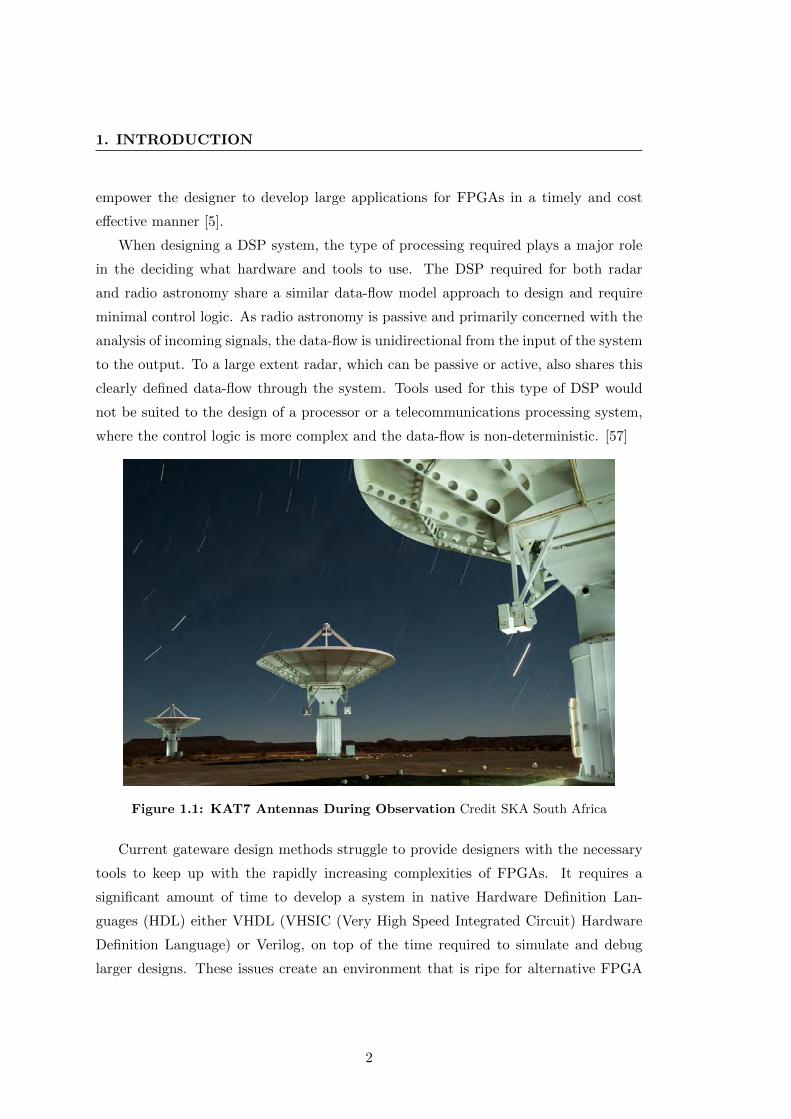
Figure 1.1: KAT7 Antennas During Observation Credit SKA South Africa
Current gateware design methods struggle to provide designers with the necessary
tools to keep up with the rapidly increasing complexities of FPGAs. It requires a
significant amount of time to develop a system in native Hardware Definition Lan-
guages (HDL) either VHDL (VHSIC (Very High Speed Integrated Circuit) Hardware
Definition Language) or Verilog, on top of the time required to simulate and debug
larger designs. These issues create an environment that is ripe for alternative FPGA
2
1.1 Problem Statement
design methodologies to gain traction and for higher-level languages, which provide
abstraction from the lower-level gateware, to flourish.
Many software development methodologies make use of object-orientation and fo-
cus on the re-usability of code. This methodology allows sections of source code to be
represented as logical objects. A similar methodology works well with FPGA develop-
ment. However, due to the static nature of hardware design, this methodology has yet
to completely mature and realise its full potential. [58]
The high level of concurrency inherent in FPGAs gives rise to the need for a very
distinct design methodology. Central Processing Units (CPU) and Graphics Processing
Units (GPU) do have a certain amount of concurrency, but at a much coarser level.
Where CPUs have full processing cores, GPUs use lighter weight kernels and FPGAs
have a designer-defined level of concurrency, which is usually much finer. Thus, sharing
design methodologies across different processing hardware does not always provide the
cleanest solution. A design-flow implementing a methodology solely targeting FPGAs
provides the optimum solution. It is this design methodology and design-flow that are
examined and implemented in this dissertation.
1.1 Problem Statement
The DBE team of the SKA-SA are responsible for designing the processing systems
for the MeerKAT and KAT-7. To do this, they currently use a tool-flow based on
Mathworks’ Matlab and Simulink environment integrated with Xilinx System Genera-
tor (XSG) with supporting script. This tool-flow was initially developed by CASPER
and used to design DSP systems for CASPER hardware. [1]
There are many aspects of the this tool-flow that work well and the features provided
to the application designers are useful. Much of the functionality has been put together
by users over the years and often requires much work to port them to newer versions of
Matlab and the Xilinx tools. There are a few key drawbacks with the current tools, in
particular licensing costs, stability and compatibility. See section 2.5 for further details.
Considering these drawbacks, the CASPER community is looking into an open-
source alternative to the Matlab, Simulink, XSG design-flow. The open-source ideology
is a part of the CASPER philosophy and the community helps with the developing of
the tools. This is important, as it allows users to add features or fix bugs themselves
3

1. INTRODUCTION
rather than having to get support from vendors and needing to wait until the next
release of a product.
Thus, it is required to research, implement and evaluate an open-source solution
to this problem. A thorough examination of existing solutions and available tools is
necessary. A tool-flow is designed from gathered requirements and its effectiveness, as
an alternative to the current CASPER design tools, used to as a measure of its success.
1.2 Project Context
This project is not undertaken in isolation, there is substantial background information
to be understood so as to put this work in context. The SKA-SA projects of KAT-7
and MeerKAT, CASPER, Mathworks and Xilinx, and the fundamentals of FPGAs and
FPGA design tools all play a significant role and give context to the work presented
here. See appendix A and appendix B for further background.
1.2.1 KAT-7, MeerKAT and SKA
Over the last decade, South Africa has become a major centre for radio astronomy,
attracting many international astronomers, scientists and engineers. This is primarily
due to the plan to build the majority of the international SKA Telescope in the Northern
Province of South Africa. The KAT-7 and MeerKAT arrays are being built as precursors
to the SKA Telescope. [1]
KAT-7 is an array of seven, 12m diameter, prime focus, reflecting antennas. It was
commissioned in 2012 and is primarily designed as an engineering test bed. However,
it is currently being used to produce science data.
The MeerKAT array is currently under construction. It has been designed as a 64-
Gregorian offset antenna array, as seen in figure 1.2. As of now, fifteen antennas have
been deployed to the site. It will support four bands: L-Band, UHF-Band, S-Band and
X-Band receivers, with the first phase implementing the L and UHF-Bands. MeerKAT
also supports a wide range of modes, including spectral imaging, beamforming, pulsar
timing and transient searching.
The MeerKAT array produces a large amount of data that needs to be processed in
real-time by the digital back-end of the array. The Analog to Digital Converter (ADC)
for the L-Band digitiser produces around 36Gbps of data per antenna. Multiplying this
by the proposed 64 antennas results in a 2.3Tbps of data to be processed in real-time.
There are a number of technologies that could be employed to do this, including CPUs,
4

1.2 Project Context
Figure 1.2: MeerKAT Gregorian-Offset Antenna Credit SKA South Africa
GPUs, FPGAs, and Application Specific Integrated Circuit (ASIC), each with unique
trade-offs.
The multiple modes of KAT-7 and MeerKAT require that the data processing back-
ends of the instruments are flexible. It would not be cost effective to process each of
the modes using a different set of hardware; a better solution would be to reconfigure
the data processing system for each of the tasks it needs to perform. As the instrument
is required to support only one mode at a time, this is viable solution.
KAT-7 and MeerKAT, as with other radio telescopes, are located in highly remote
areas, thus electrical power is costly and difficult to acquire. Thus, the power consump-
tion of the DSP system is a high priority. FPGAs tend to do well in this area as they
are particularly low on power consumption when compared to GPUs and CPUs. [1]
1.2.2 The Role of FPGAs in Radio Astronomy
Radio astronomy data processing faces two challenges. Firstly, a large compute capacity
and secondly, high bandwidth communications. Each of these challenges has been
solved individually in industries such as telecommunications (high bandwidth) and
super computing (large compute capacity) but there are few applications which require
5
1. INTRODUCTION
both simultaneously. This is where high-end FPGAs come to the fore. FPGA vendors
offer a wide range of devices covering a high I/O bandwidth and large compute capacity.
These devices are well-suited to radio astronomy applications such as antenna array
correlation, wide-band spectroscopy and pulsar surveys. [7] [8]
There are many design constraints inherent in radio astronomy instrumentation.
Most radio astronomy installations are required to be in radio quiet areas which are
generally very remote locations as far from human habitation as possible. The sec-
ond major restriction is due to Radio Frequency Interference (RFI), particularly self-
generated RFI. Due to the lower power consumption and fewer clocks, FPGA-based
processing systems produce less RFI than GPUs and CPUs. With controllable clocking
sources, the FGPA can be run at a frequency with harmonics that are outside of the
band of interest to astronomers, further reducing RFI. [7] This is not possible with
CPUs or GPUs.
However, it is important to note that GPUs are developing quickly and are becoming
better-suited to certain types of processing, particularly floating point numeracy, which
FPGAs are not suited to. This makes a hybrid instrument consisting of both FPGAs
and GPUs more favourable. With the CASPER approach of Ethernet interconnects,
this is entirely possible.[1] See appendix A.
1.2.3 CASPER: A Collaborative Ideology
World-wide, radio astronomy is a relatively small industry and often has to rely heavily
on government funding. It is therefore beneficial to share resources between organisa-
tions as to leverage the work that others have put into developing radio astronomy
instrumentation. As there is minimal financial incentive to invest radio astronomy,
organisations are often able to open source their intellectual property. CASPER was
founded to aid this collaboration. It aims to share and collaborate on both hardware
and software for the design of radio astronomy DSP systems. [8]
The CASPER community has designed multiple FPGA boards, including the ROACH2
hardware platform. It was designed by the DBE team of the SKA-SA. The ROACH2
platform supports up to two high speed ADCs and eight 10Gbps ports. The board is
controlled by a processor running a light version of Linux. This allows the FPGA to be
programmed via the processor from a remote location. The FPGA is a Xilinx Virtex
6
1.2 Project Context
6 which has around four times more resources than the previous version, the Virtex 5.
See appendix B for detailed specifications of the Virtex 5 and Virtex 6 FPGAs.
Along with hardware platforms, CASPER provides a tool-flow based on the Matlab,
Simulink and XSG tools to enable a designer to easily design and target a particular
hardware platform. [66] The interface is a graphical design environment in Simulink
where a designer can drag and drop blocks and connect them with wires in the desired
configuration. A library of CASPER DSP blocks are provided. These are targeted at
the particular type of DSP typical of radio astronomy data processing. In addition,
there is also a library of hardware specific blocks, which contain the controllers for
ADCs and Ten Gigabit Ethernet (TGE) modules, amongst others. The flow provides
a ”One-Click” solution from design to bitstream, ready to upload onto a board. The
DSP parts of the design are easily transferable to other Xilinx FPGA hardware. This
eases upgrades to new hardware, as well as aiding collaboration between teams using
different CASPER hardware platforms. [8]
CASPER makes use of a generic backplane architecture and uses standard Eth-
ernet to provide packetised interconnects between hardware modules. In this way,
instruments can consist of different types of data processing hardware. For example,
it is easy to hand off parts of the processing chain to a GPU cluster by redirecting
the data sent over the network to different Internet Protocol (IP) address. The data
in the MeerKAT system is transported over the network using IP Multicast protocol1
which allows additional instruments to subscribe to the data and process it concur-
rently alongside the main instrument. [8] With Moore’s Law 2 dictating the growth of
processing, it is necessary to be able to upgrade the system every so often, to lever-
age these benefits. When the next generation ROACH board is realised, it is easy to
replace the older hardware with newer hardware, as they both use Ethernet as their
interconnects. This keeps the problem of full cross-bar interconnects in the domain of
the switch manufactures and allows instrument designers to focus on DSP. [1] [65]
Overall, CASPER has a progressive philosophy towards instrumentation design and
it is important to take into account when examining, designing and implementing tools
to be used by this community and others.
1IP multicast is described in RFC 11122Moore’s Law states that the number of transistors in an integrated circuit double approximately
every two years
7

1. INTRODUCTION
1.3 Objectives
The objective of this dissertation is two fold. Firstly, to gauge whether MyHDL is an
appropriate tool around which to design a framework for FPGA development. Secondly,
to determine whether the current CASPER tool-flow methodology and architecture is
a suitable framework for the new tool-flow.
The CASPER tool-flow uses the Model-Driven Development (MDD) approach with
a Graphical User Interface (GUI) to design for FPGAs. The architecture consists of
sets of library blocks,hardware base projects and a set of tools to manage the design
and integrate the vendor’s tools into the flow.
The objective is to examine whether MyHDL, together with a Python-based frame-
work can be used as a tool-flow for radio astronomy DSP design on FPGA hardware.
Hypotheses:
• MyHDL is a viable open-source tool around which to build a design-flow framework
for FPGA development, targeting radio astronomy DSP.
• The current CASPER design methodology combined with MyHDL is suitable for
the new tool-flow.
1.4 Approach
The approach taken to achieve these objectives is as follows:
An examination of FPGA design methodologies is undertaken. This serves to pro-
vide an understanding of other methodologies, so that they can be compared to MDD.
An examination of the available proprietary and open-source tools is undertaken. This
aids to highlight important features of other tools. The inner workings of MyHDL are
then discussed, in order to provide an understanding of how MyHDL uses Python as
an HDL language.
To show that MyHDL can be used in a framework as described in section 1.3, aspects
of such a tool-flow are designed and implemented. Before designing the tool-flow, the
requirements are gathered, analysed and then a design specification compiled.
Certain aspects of the design specification are implemented. Then the tool-flow is
used to create three example FPGA designs, each of which is carefully chosen to test
exerciser specific functionality of the tool-flow.
8

1.5 Methodology
The results of each design are examined and evaluated to show how successfully the
tool-flow meets the objectives. The tool-flow is also evaluated against certain metrics,
in particular ease-of-use and reliability. See section 3.4.2 for the full list of metrics.
1.5 Methodology
The overarching requirement is to evaluate MyHDL as an open-source tool around
which a framework can be created to aid in designing Field Programmable Gate Array-
based (FPGA) Digital Signal Processing (DSP) systems for radio astronomy instru-
mentation.
The means of testing is decided on. The tool-flow will be tested by creating example
designs to test specific functionality. The areas that will be tested are the incorporation
of vendor tools, memory-mapped bus creation and simulation of a DSP design. The
analysis of certain metrics, such as ease of use and development time, is also used to
test the success of the tool-flow.
The constraints and assumptions are noted and considered in the subsequent steps.
As with any project, there are limitations and constraints. The two major constraints
for this project are that MyHDL is the tool to be used and that the architecture of the
current CASPER tools is used.
The next step is to gather detailed requirements for the new tool-flow. These are
collected from sources such as the CASPER mailing list, DSP engineers working on
MeerKAT and discussions held at the annual CASPER workshops.
The gathered requirements is a list of useful features, but needs to be distilled into
workable requirements and then into a design specification.
Due to the scope of this project, only select requirements are implemented. These
requirements are selected carefully, so as to focus on particular key areas. It is important
that these areas are shown to work correctly as they are fundamental to the tool-flow
being a success. These requirements are discussed in detail.
The selected requirements are then designed and implemented. This process, the
problems encountered and the solutions are discussed and explained.
To test particular aspects of the tool-flow, example designs are created. These
target the key areas of the tool-flow and help to gauge the success of the tool-flow.
Each of the example designs is simulated to ensure that it functions as expected.
The simulations for each design are analysed and explained.
9
1. INTRODUCTION
The example designs are compiled and deployed on hardware. They are run with
the same stimuli as the simulations and the outputs again analysed and discussed.
It is important to compare the simulation results with the hardware results. This
gives a clear picture of the accuracy of the simulations and allows the success of the
tool-flow to be gauged.
The results of the test designs are analysed and used to measure to what extent the
objectives are met. The metrics established prior to the design of the tool-flow are mea-
sured and discussed. The implemented features are evaluated against the requirements
and the overall success of the project determined.
1.5.1 System Design Approach
Before designing and implementing large systems, it is important to have a good un-
derstanding of the problem space and the requirements. This project follows two very
widely used design methodologies, the Waterfall Method and System Engineering ap-
proach. These methods are chosen because they are widely used techniques for design-
ing, implementing and testing systems and the author is familiar with them.
A diagram of The Waterfall Method can be seen in figure 3.2. The instance used
in this project consists of six stages: requirements gathering, requirements analysis,
design specification, implementation, testing and verification, and maintenance. The
design process follows these steps in their respective order. If an issue is found at any
stage one or more steps can be taken back up the waterfall and the issue fixed at that
stage, which then trickles back down the waterfall, through each of the stages. [59]
Firstly, the requirements are gathered from features of the existing tools, other
tools, current users and the CASPER mailing list. These requirements are then anal-
ysed and given a level of complexity and priority. This determines when it will get
implemented and how important it is. It is at this stage that some requirements are
possibly discarded, as not all requirements can be met. In this project, only a subset of
the requirements are implemented, as the scope of the project is restrained do to time
constraints.
A design specification is then created from these requirements. This process
fleshes out the requirements and explains how each is going to be achieved. At this
stage, there are also some assumptions made, which put constraints on how the re-
quirements are implemented. For example, the use of Python as the framework for the
10

1.5 Methodology
Figure 1.3: Waterfall Methodology Diagram [59]
11
1. INTRODUCTION
tool-flow is a prerequisite.
Once the design specification is complete, the implementation can begin. It is
important to note that during implementation it is often realised that it may not be
possible to implement certain functionality the way it is designed. This will feed back
up to the design specification and the requirements stages and will need modification
before coming back to implementation. The Waterfall Method allows the process to
move back up-stream if there are issues that need to be addressed at a previous stage.
During implementation, testing also occurs. This is a cyclic process between testing
and implementation, until ultimately all the requirements are met and the system can
move into a maintenance phase. It is seldom that software remains static for very long,
as often features are added or bugs need fixing and the implement-test cycle continues.
As with any piece of software, there will always be maintenance. This takes the
form of bug fixing and upgrades to keep the tool-flow up-to-date and functioning with
the latest vendor tools. Hence, maintenance is an ongoing process.
1.6 Scope and Limitations
This project will not implement the entire tool-flow as that is too large a task for the
scope of a Masters. A range of selected features are implemented and tested by the
example designs. This means that some parts of the flow are implemented manually.
One such manual task is connecting the DSP design to the base package.
As MyHDL is the tool under examination, other tools are examined but not in
depth. MyHDL was chosen as it is the most mature of the open-source tools and it is
written in Python, a language that many researchers and academics are familiar with.
The architecture methodology of the tool-flow is kept similar to that of the current
CASPER tools. See section 1.3. This is because CASPER users are familiar with the
methodology and architecture, and it has been proven to work well.
The design of the Finite Impulse Response (FIR) filter in section 5.3 is purely a test
case to ensure that the simulation and hardware results match. Therefore, the theory
of FIR filters is not dealt with in this project.
1.7 Chapter Outlines
This section outlines the chapters of this dissertation. The structure of these chapters,
and their summary presented here, have been designed to provide a coherent overview
12
1.7 Chapter Outlines
of the write-up.
Chapter 2 - Literature Review
This chapter examines how HDLs have evolved since their inception, including the
more recent trends of FPGA design methodologies. It briefly discusses the available
open-source and proprietary tools for FPGA development. Finally, it provides an in-
depth overview of MyHDL.
As the size and complexity of FPGAs increases, so do application designs and the
time taken to develop them. Developers are constantly seeking ways to ease the design
of FPGAs and reduce implementation time. There is a push to use more traditional
programming languages for hardware design. Some of the more popular implementa-
tions are OpenCL, SystemC and MyHDL. Tools like these aim to provide a larger set
of features to the designer, but the design still needs to be converted to HDL and then
to Register Transfer Level (RTL) as intermediate steps. [50]
Gateware design tools can be divided into different methodologies. Many of these
tools fall into multiple categories, partly due to overlaps between methodologies. A
language can use either the event-driven paradigm or the actor-object model, and can
be one or more of the following: an object-oriented language, domain-specific language
or a model-based tool.
MyHDL is the tool chosen around which a framework is developed. It is an open-
source Python package that enables Python to be used as an HDL. It does this by using
the Yield, Generator and Decorator functionality inherent in Python. MyHDL code
can be converted to either Verilog or VHDL and then implemented onto silicon using
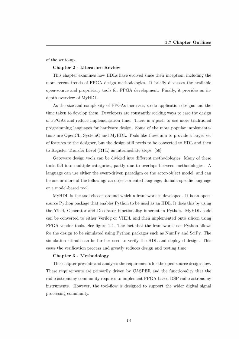
FPGA vendor tools. See figure 1.4. The fact that the framework uses Python allows
for the design to be simulated using Python packages such as NumPy and SciPy. The
simulation stimuli can be further used to verify the HDL and deployed design. This
eases the verification process and greatly reduces design and testing time.
Chapter 3 - Methodology
This chapter presents and analyses the requirements for the open-source design-flow.
These requirements are primarily driven by CASPER and the functionality that the
radio astronomy community requires to implement FPGA-based DSP radio astronomy
instruments. However, the tool-flow is designed to support the wider digital signal
processing community.
13

1. INTRODUCTION
The design process follows the Waterfall and System Engineering methodologies as
detailed in section 1.5.1. The progression from the requirements to the design specifica-
tion is explained. The chapter then describes the ideas underlying the tools and explains
the ideas and reasoning behind key design decisions. It then links these decisions back
to the requirements.
The design specification splits the tool-flow into three functional sections: the Base
Designs, the Libraries and the Framework. Each of these sections is described and
the process from requirements to design is explained. Selected requirements for the
tool-flow are examined in depth and the implementation explained.
Chapter 4 - Design and Implementation
This chapter details the implementation of the tool-flow, also showing how the
implementation links back to the requirements. It examines: the clocking and bus
architectures in the base project and the design of select library blocks. It also explains
the more important aspects of the framework scripts.
An overview of the architecture is given and discussed in detail, with focus on the
architecture diagram in figure 1.4. It shows how all aspects of the tool are incorpo-
rated into the design-flow, with particular emphasis on the libraries, base project and
framework.
As the design of the tool-flow is a relatively large piece of work, only certain func-
tionality is implemented. There is a focus on the libraries, bus and clocking infrastruc-
ture, integration with vendor tools and base designs. The remaining functionality is
discussed, but not implemented.
Chapter 5 - Case Studies
In order to demonstrate the functionality of the tool-flow, three case study designs
have been implemented. The first of which is a very simple counter Light Emitting
Diode (LED) design. The second is more complex and requires multiple library blocks
structured as to assess the simulation framework and exercise a wider range of FPGA
elements. It includes memory-mapped bus devices. Finally, a more complex design
demonstrates the ability of the Tool-flow to aid with the design and simulation of a
DSP system.
The first design is a basic counter whose outputs are connected to LEDs on the
FPGA board. See figure 5.1 on page 106. This tests the fundamental concept of the
tool-flow, that the flow can take a design from a model to to implemented gateware
14
1.7 Chapter Outlines
Figure 1.4: Architecture of the CASPER tools
15
1. INTRODUCTION
running on the FPGA. This ensures that the the vendor tools are integrated correctly
and the passing of the design to these tools is functioning smoothly.
The second design is a simple adder. See figure 5.3 on page 110. The design consists
of three registers which are connected to the memory-mapped bus. Two of the registers
are added together and the result written into the third register. The aim of this design
is to test that the memory-mapped bus implementation is working as expected and that
is it translated into hardware correctly.
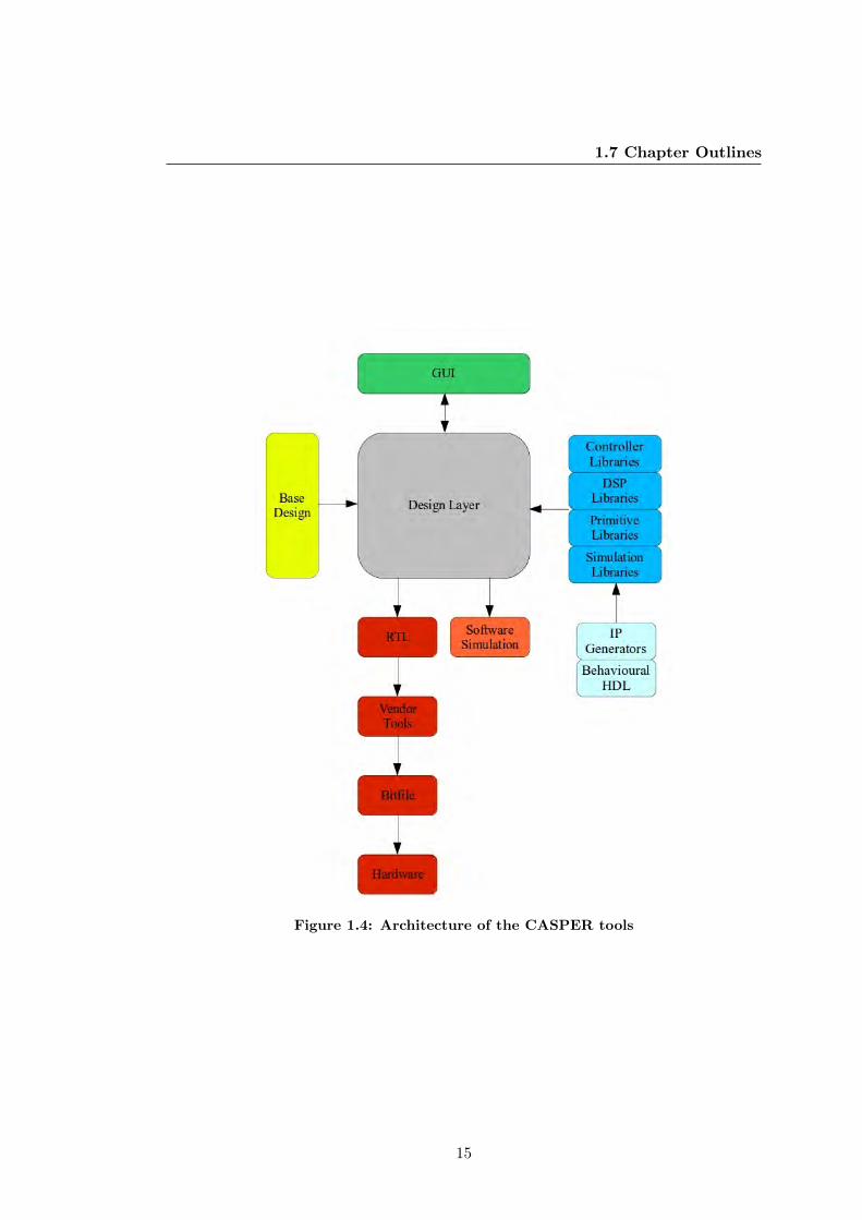
The third design is a more complex DSP system consisting of a low pass Finite
Impulse Response (FIR) filter. See figure 5.4 on page 113.. The filter receives data
from the ADC and once filtered, stores it in a Block Random Access Memory (BRAM).
This BRAM is accessible via the memory-mapped bus, which can be read via the on-
board processor. The output is then plotted using Python tools. The filter is simulated
and tested in hardware by injecting a signal consisting of two mixed sinusoidal waves.
One sinusoidal wave within the passband and the other outside. The output of the
filter shows a reduction in the power of the out-of-band signal, while the in-band signal
retains its power.
Chapter 6 - Results and Conclusions
This chapter examines the results of the three example designs, it compares the
simulation outputs to that of the hardware implementations. It then discusses the
objectives of the project and the extent to which they are met. The metrics to measure
the success of the tool-flow are discussed and the project summarised.
The first example design shows that the tool-flow successfully integrates the Xilinx
tools into the flow.
The results of the memory-mapped adder example design are compared to the
hardware implementation and are found to be as simulated. This is a successful test of
the memory-mapped bus infrastructure and proves that the bus generation is working
as expected.
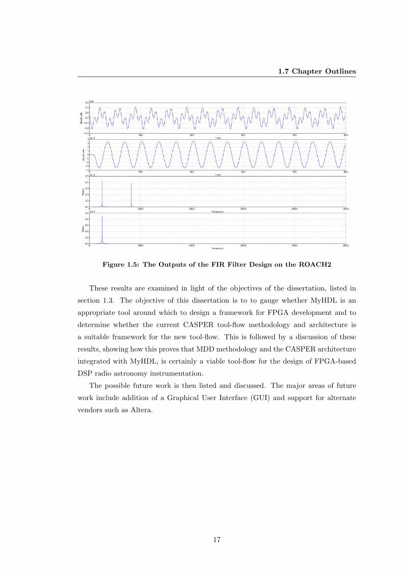
The input to the ADC and FIR filter design is a mixed signal consisting of two
sinusoidal waves, one inside the passband and the other outside of the passband. The
output of the filter shows primarily the in-band tone remaining and the out-of-band
tone being filtered almost completely. Figure 1.5 shows the plots of the outputs of the
FIR filter design. These results match the Python simulation of the filter and prove
that the filter is working as designed and that the tool-flow functions as expected.
16
1.7 Chapter Outlines
Figure 1.5: The Outputs of the FIR Filter Design on the ROACH2
These results are examined in light of the objectives of the dissertation, listed in
section 1.3. The objective of this dissertation is to to gauge whether MyHDL is an
appropriate tool around which to design a framework for FPGA development and to
determine whether the current CASPER tool-flow methodology and architecture is
a suitable framework for the new tool-flow. This is followed by a discussion of these
results, showing how this proves that MDD methodology and the CASPER architecture
integrated with MyHDL, is certainly a viable tool-flow for the design of FPGA-based
DSP radio astronomy instrumentation.
The possible future work is then listed and discussed. The major areas of future
work include addition of a Graphical User Interface (GUI) and support for alternate
vendors such as Altera.
17

1. INTRODUCTION
18

Chapter 2
Literature Review
To put this dissertation in context, it is necessary to have a good understanding of a few
areas of study. which includes a comprehensive understanding of Field Programmable
Gate Array (FPGA) technologies and design tools. It is assumed that the reader has
a comprehensive knowledge of FGPA technologies and the processes by which vendor
tools convert a Hardware Definition Language (HDL) design to a bitstream, to be
uploaded onto a device. A detailed explanation of this is can be found in Appendix A
The literature review covers HDLs and how they have evolved to use different de-
sign methodologies, how this helps to conceptualise the concurrency inherent in FGPA
technologies. A discussion of existing tools is provided, with a focus on open-source
tools and previous work in this area. Following this, MyHDL is explained and analysed
in depth, with particular emphasis on how it allows the design of concurrent systems
using a sequential software language.
2.1 HDL Trends
To understand the future of HDLs design methodologies, their history and the roles they
were originally designed for need to be examine. Currently, the two major languages
used to design for FPGAs are Verilog and VHDL. Both were developed in the 1980’s
and are still used today to describe and model hardware. While there have been
a few updates to both languages over the years, they are still very limited. This
is in part due to the nature of hardware which allows only certain constructs to be
synthesisable, although there are many features which would aid designers that are yet
to be implemented. [60]
19
2. LITERATURE REVIEW
As the size and complexity of FPGAs increase, so too does the complexity of de-
signs. Developers are constantly seeking ways to ease the design of FPGAs and reduce
implementation time. This prompts a move towards using more traditional program-
ming languages for hardware design. Some of the more popular implementations being
SystemC and MyHDL. Tools like these aim to provide a larger set of features to the
designer, but are still stuck having to convert the design to HDL and then to Register
Transfer Level (RTL) as intermediate steps.
Synthesis tools can be likened compilers of the 1970’s. There is still significant
development required to make them efficient and optimised to the degree that the
underlying implementation can be trusted. The compilers of today are efficient enough
that the machine code generated is better optimised than could be done by hand.
FPGA vendors have invested significant time and resources into their synthesisers,
mapping and place and route tools as larger FPGAs require better algorithms to manage
designs for larger chips timeously.
Modern software languages support many features such as maths functions, like
Fast Fourier Transforms (FFT) and Filters, which would make verification of HDL
designs easier. Software languages also have a more concise syntax. The object-oriented
methodology which is supported by many software languages is also good mechanism
by which to model hardware. [58]
Realistically, it will be a while before a new standard for a hardware design language
is widely adopted. Current trends are moving away from HDLs to higher level languages
such as SystemC, OpenCL, Python and Matlab. [30] Although, the effort is split across
many languages, ultimately only a couple will be adopted by the community and become
widely used. It is an interesting time for hardware design, and FPGA vendors will play
a large role in deciding which way things will go. However, until then designers will
need to select tools which they feel can best aid their design requirements and will need
to work within the limitations of existing tools.
2.1.1 HDL Developments
Initially HDLs were developed to aid design and simulation of hardware systems. The
original developers had proprietary simulators which synthesised and simulated either
VHDL or Verilog. Now, HDLs are used primarily to describe Application Specific
20
2.1 HDL Trends
Integrated Circuit (ASIC) or FPGA designs and there are a number of simulators
available for each. [61]
The development of HDLs has not been entirely static. There have been revisions
to the languages over the years to implement new features. Although the language
standards may specify new features, there is normally a delay before vendors start to
support them in their synthesis tools.
This constant revision of the Verilog and VHDL standards is very necessary and has
provided designers with more and more features which aid design. However, with the
complexity of hardware following an almost exponential curve, it is a paradigm shift in
design methodology that is required, not only additional features.
2.1.1.1 Verilog
Over the years there has been development on the Verilog Standard Institute of Elec-
trical and Electronics Engineers (IEEE) 1364. The language has evolved slowly with
the largest changes coming in the latest System Verilog specification.
Verilog was ultimately standardised in 1995 and is now known as the IEEE 1364-
1995 Standard or Verilog-95. Subsequently, this standard has been updated in the IEEE
1364-2001 standard also known as Verilog 2001.1 The specification was most recently
updated again in 2005, to the IEEE 1364-2005, to iron out a number of bugs and further
clarify the specification. With the most notable changes being the generate statement
to allow more flexibility within modules and the introduction of a more concise and
clean syntax for module declaration. [35] [34] [28]
In 2009, the System Verilog Specification was standardised in IEEE 1800-2009. The
idea was to provide more features to aid in modelling and verification of designs. It
allows classes and parts of object-oriented design features to be used when modelling
and verifying designs. It also provides a mechanism by which signals can be grouped
as buses or interfaces, and be passed between modules without having to specify each
port/wire on the bus individually. [32]
These constructs, amongst others, give the designer tools that are not available with
the traditional Verilog. Unfortunately, FPGA vendors often take time to providing
support for the updates to HDLs which prevents the designer from fully utilising the
power of additional features.
1http://www.asic-world.com/verilog/history.html
21

2. LITERATURE REVIEW
2.1.1.2 VHDL
VHDL was initially developed by the US Department of Defense in 1981 in an effort
to address the hardware life-cycle crisis. It was later given to the IEEE to encourage
industry adoption.1
The first standardised version of VHDL came about in 1987 and is know as IEEE
1076-1987 or VHDL-87. There were a further three revisions to the standard, IEEE
1076-1993, IEEE 1076-2002 and IEEE 1076-2008 which is the current VHDL standard
and is also know as VHDL 2008 or VHDL 4.0.2 [36]
With the high number of revisions to the VHDL standard, the language supports
a larger feature set than Verilog, although at the same time being more verbose. For
example, VHDL requires a component architecture as well as the component declaration
to be specified, this is redundant as it duplicates information.
2.1.2 High Level Synthesis (HLS)
The hardware behind any data processing system can usually falls into one of four major
domains, Central Processing Units (CPU), Graphics Processing Units (GPU), Digital
Signal Processors (DSP) and FPGAs/ASICs. Each of these domains requires a different
design methodology or paradigm. The main feature which sets these domains apart is
the level of parallelism inherent in each. For example,CPU) have only recently become
multi-core processors, in programming languages targeting CPUs there is the concept
of threads and processes. These are still quite heavy when compared to the concept
of kernels when if comes to GPU programming. Even lighter then GPU kernels is the
concept of parallelism within FPGAs. An entirely different programming methodology
is needed and hence, different languages to target each domain. Verilog and VHDL
do a good job at targeting FPGAs but are still lacking a higher level approach that is
required for timeously implementing an FPGA design.
More recently there is a trend towards modelling hardware in a software language
or HLS (High-Level Synthesis). This is not always ideal as the language has generally
been designed with CPUs in mind and not FPGAs. Although this certainly makes
design verification quicker and simpler. Ultimately the HLS still needs to be converted
1http://www.doulos.com/knowhow/vhdl designers guide/a brief history of VHDL/2http://www.ustudy.in/node/3403
22

2.1 HDL Trends
to either Verilog or VHDL before synthesis, this adds another layer of complexity into
the design process.
There are a number of attempts to use languages across domains, particularly when
it comes to High-Level Synthesis for FPGAs. SystemC and C to Gates use a subset
of the C or C++ languages to model hardware and there is even a flavour of OpenCL
which is designed to target GPUs.
1 template<class coef_T, class data_T, class acc_T>
2 data_T CFir<coef_T, data_T, acc_T>::operator()(data_T x) {
3 int i;
4 acc_t acc = 0;
5 data_t m;
6
7 loop: for (i = N-1; i >= 0; i--) {
8 if (i == 0) {
9 m = x;
10 shift_reg[0] = x;
11 } else {
12 m = shift_reg[i-1];
13 if (i != (N-1))
14 shift_reg[i] = shift_reg[i - 1];
15 }
16 acc += m * c[i];
17 }
18 return acc;
19 }
Listing 1: Vivado HLS C++ FIR Filter - Designed for an FPGA [30]
An issue inherent with Higher-Level Languages is that it still needs to be converted
to either Verilog or VHDL, which is, in turn, synthesised into Register Transfer Level
(RTL) which is then mapped to available resources and placed and routed. This process
has a a number of complex steps and requires mature HLS to HDL conversion tools.
While, HLS is a very useful tool, it is required to mature further before it is likely to
23
2. LITERATURE REVIEW
see wide-spread adoption.
2.2 Gateware Design Methodologies
Gateware design tools can be divided up into different methodologies. Many tools
can even fall into multiple categories, partly due to overlaps between the different
methodologies. A design tool can fall into either the event-driven paradigm or the actor
object model, and can be one or more of the following: an object-oriented language,
Domain-Specific Language (DSL) or a model-based design tool.
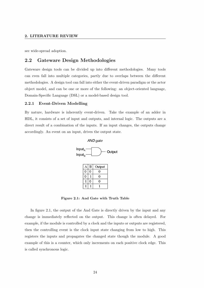
2.2.1 Event-Driven Modelling
By nature, hardware is inherently event-driven. Take the example of an adder in
HDL, it consists of a set of input and outputs, and internal logic. The outputs are a
direct result of a combination of the inputs. If an input changes, the outputs change
accordingly. An event on an input, drives the output state.
Figure 2.1: And Gate with Truth Table
In figure 2.1, the output of the And Gate is directly driven by the input and any
change is immediately reflected on the output. This change is often delayed. For
example, if the module is controlled by a clock and the inputs or outputs are registered,
then the controlling event is the clock input state changing from low to high. This
registers the inputs and propagates the changed state though the module. A good
example of this is a counter, which only increments on each positive clock edge. This
is called synchronous logic.
24

2.2 Gateware Design Methodologies
Both Verilog and VHDL use the event-driven paradigm. Verilog uses the always@
keyword to denote which signals drive the logic. This creates a sensitivity list (a
list of signals that if they change state the state is propagated through the module).
Although, not all inputs are necessarily part of this list. HDLs also have the concept of
combinatorial logic, meaning that all input signals are included in the sensitivity list.
An And gate is a basic example of this.
1 always @(posedge clk) begin
2 ...
3 <Sequential Code>
4 ...
5 end
Listing 2: Verilog Sensitivity List
HDLs use the event-driven paradigm as it models exactly how hardware behaves. It
is a lower-level approach and with the growth of FPGAs in size and complexity, there is
a move to abstract this from the designer and provide a higher-level approach to FPGA
design. However, this comes at the expense of finer control over design implementation.
2.2.2 Actor Model
The Actor Model can also be described as a streaming model. A design is broken up
into processing nodes which are connected together via a streaming bus interface. The
lowest level primitive is an individual node. This allows the design to be viewed at a
higher level as a set of nodes which interconnected with buses.
Figure 2.2 shows a design layout using the actor model. The arrows represent the
streaming data bus which coordinates the transfer of data between the processing nodes
(actors). The bus would generally support a mechanism of back pressure, by which a
node can tell source node to stop sending more data until it completes processing the
current data.
In a typical KAT-7 or MeerKAT system, the initial actor would be either an ADC,
sampling a signal, or a Ten Gigabit Ethernet port receiving data. The final node would
be a Ten Gigabit Ethernet port which would be sending the data on for storage for
25
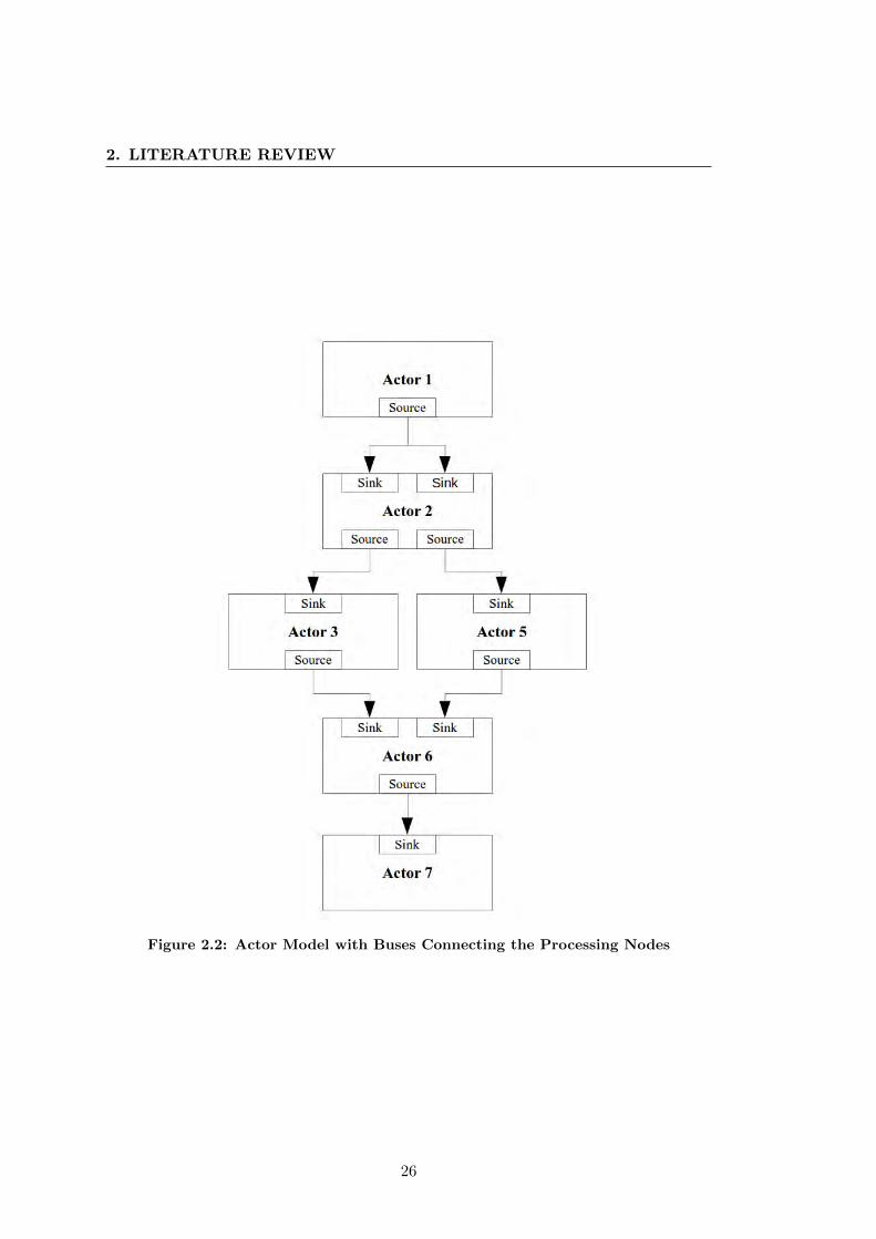
2. LITERATURE REVIEW
Figure 2.2: Actor Model with Buses Connecting the Processing Nodes
26

2.2 Gateware Design Methodologies
further post-processing. The middle nodes actors would typically be processing nodes
such as FFTs, wideband Polyphase Filter Banks (PFB), quantisers or corner turners.
This methodology of viewing the design as a set of data processing nodes, abstracts
the designer away from the lower level of having to manage clocks, resets and imple-
mentation details. However, this does require that the library of actors/nodes exists
prior to design time. Although, there is nothing stopping the designer from adding and
customising libraries.
2.2.3 Domain-Specific Languages (DSL)
A DSL is a language that is designed to specialise in a particular domain, as opposed to
a general purpose language. A good example of a DSL is Hyper Text Markup Language
(HTML), used specifically to create web pages.
Often DSLs exist within a language framework. For example, Delite provides com-
pile and runtime framework in which DSLs can be easily created. Delite uses the
SCALA language on which to base the framework on. OptiML, OptiQL and Liszt are
a three other DSLs created using the Delite framework which target: machine learning,
data analytics and physics respectively. [23]
Both radio astronomy and radar data processing systems are good candidates for
a DSL due to the unique type of data processing required. Radio Astronomy often
requires wideband signal processing such as PFBs and FFTs.
The creation of a DSL involves defining a set of functions or libraries for a specific
task. Often the base language is extended by the DSL. Ultimately, DSLs define a set of
functions/libraries that are tailored to a specific domain. In this regards this is similar
to the Model-Driven Development (MDD) methodology.
2.2.4 Model-Driven Development (MDD)
Much research and discussion has gone into the field of MDD in terms of designing
software applications.It has long been thought that by now the majority of software
development would be done using some form of MDD. This however, is not the case.
This is different in hardware design which is adopting the MDD methodology much
more rapidly as it is better suited to the this paradigm than software development.
This is largely due to the structured nature of hardware designs as opposed to the large
range of flexibility and customisations that is afforded by software development. [21]
27
2. LITERATURE REVIEW
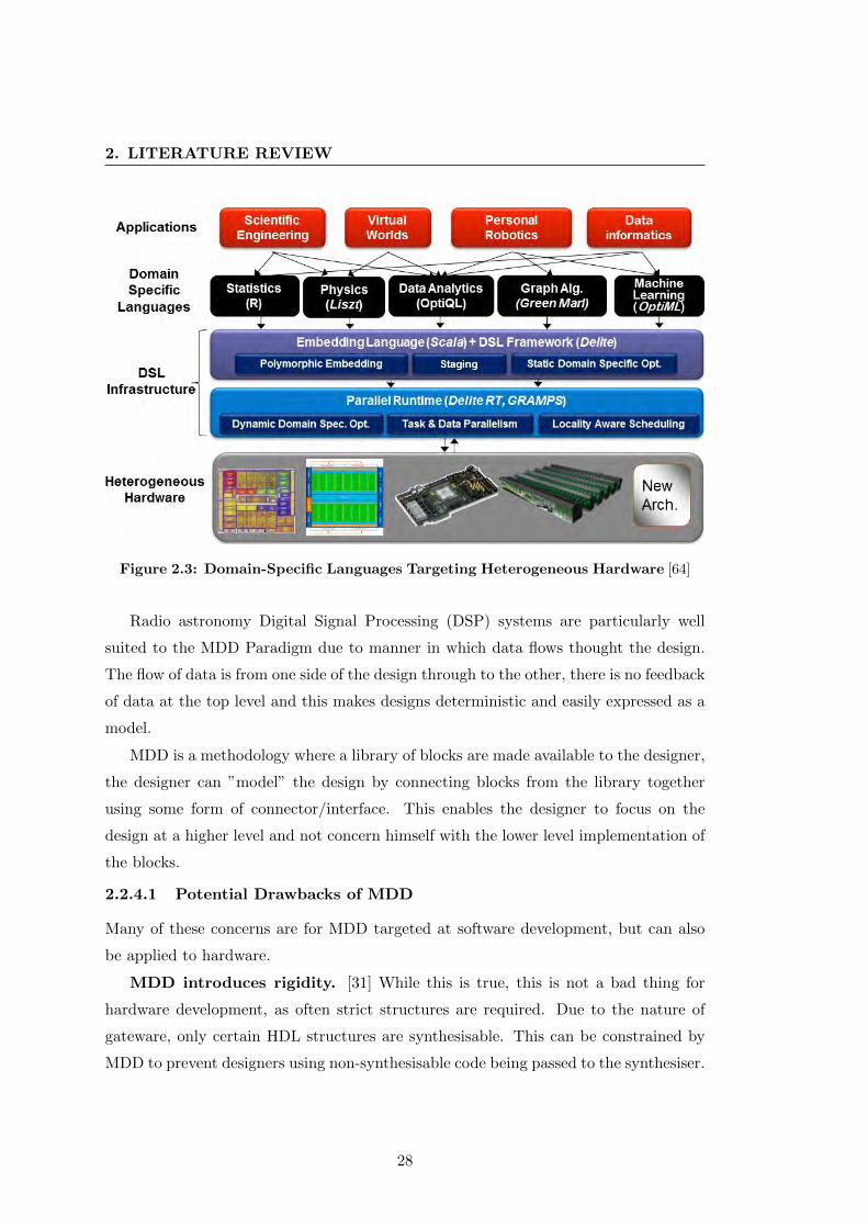
Figure 2.3: Domain-Specific Languages Targeting Heterogeneous Hardware [64]
Radio astronomy Digital Signal Processing (DSP) systems are particularly well
suited to the MDD Paradigm due to manner in which data flows thought the design.
The flow of data is from one side of the design through to the other, there is no feedback
of data at the top level and this makes designs deterministic and easily expressed as a
model.
MDD is a methodology where a library of blocks are made available to the designer,
the designer can ”model” the design by connecting blocks from the library together
using some form of connector/interface. This enables the designer to focus on the
design at a higher level and not concern himself with the lower level implementation of
the blocks.
2.2.4.1 Potential Drawbacks of MDD
Many of these concerns are for MDD targeted at software development, but can also
be applied to hardware.
MDD introduces rigidity. [31] While this is true, this is not a bad thing for
hardware development, as often strict structures are required. Due to the nature of
gateware, only certain HDL structures are synthesisable. This can be constrained by
MDD to prevent designers using non-synthesisable code being passed to the synthesiser.
28

2.2 Gateware Design Methodologies
Flexibility needs to be designed in. [31] When designing an MDD set of
libraries there is a need to design for re-usability and flexibility. In hardware design this
can be achieved by parameterising the data and address width on the block interfaces.
Although, there is a fine line between providing enough flexibility and over-engineering
a block. Ideally the block should cover about 80 to 90 percent of the uses cases, with
corner cases left up to the designer to take care of.
Version control of the model design is a hard task. [31] In the past, this has
been an issue, as many proprietary MDD design applications save designs as binary
files which do not do well with revision control systems. A well-tested solution to this
problems is to use the Extensible Markup Language (XML) to store designs. It is plain
text and therefore is human readable and diffable.
When creating an MDD environment and library it is key to get the
granularity correct. Coarser-grained modules provide less flexibility, but allow for
higher-level design. Whereas, finer-grained modules allow for more flexibility, but re-
quire more design work.
2.2.4.2 Strengths of MDD
Easy to learn and start using. The MDD methodology abstracts the designer
away from the lower level aspects of a design, allowing the designer to focus on the
functionality of the design rather than the underlying implementation. This lets a
new designer start designing with very little knowledge of the hardware architecture on
which the system is to be deployed. [11]
High Level Focus. MDD allows a designer to work at a higher-level and therefore,
the step from the system architecture specifications to the implementation is smaller.
If the designer does not need to worry about clock domains, reset architecture and bus
infrastructure, then the design process is largely simplified.
Rapid development times. Due to the existing block libraries, the time to design
a working and tested system is reduced, as much of the required functionality exists
and just needs to be incorporated into the design. This encourages the sharing of IP
and collaboration, reducing design time and allowing the designer to focus on algorithm
implementation, rather than low level intricacies.
Easily understood designs. A block diagram is easily understood, even by
someone unfamiliar with the design. This reduce the time required when handing
29

2. LITERATURE REVIEW
over designs between designers. This also lends itself to collaboration as it is easier to
understand what another designer has implemented and to incorporate it into other
designs.
Easily reusable code. If the interfaces to a module are clearly defined, then it is
easy to port modules between designs again, lending itself to collaboration and design
reuse.
2.3 Proprietary Tools
Often third parties provide their own tools which interface to FPGA vendor’s tools.
For example, Matlab has Simulink and HDL Coder. These tools generally serve to add
functionality to the existing vendor tools.
2.3.1 Matlab, Simulink, Xilinx System Generator
The Mathworks Simulink package is a graphical environment in which systems can be
designed and modelled. Both Xilinx and Altera supply plug-ins for Simulink. Each of
these plug-ins provides a set of FPGA-synthesisable libraries which can be pulled into
Simulink as blocks and connected to other blocks as required. The plug-ins then allow
the designer to generate the design, which puts it into a format that can be incorporated
into a Xilinx/Altera project with the necessary controllers to form a complete system.
Then the rest of the design can be synthesised and a bitstream generated.
This is a useful tool as it opens up the Simulink blocksets to be used to simulate
and verify these HDL designs. Simulink provides input stimuli, scopes and a range of
other non-synthesisable blocks to aid in the design, testing and simulation processes.
CASPER has leveraged off this and written a tool that provides flexible DSP li-
braries built from Xilinx primitives and a set of controller libraries. The CASPER tools
also have scripts to generate and connect the libraries into a base project which targets
the desired hardware platform. Altogether, this provides a one-click solution to take
a design to the bitstream to upload onto an FPGA, rather than having to import the
DSP design into another project. See section 2.5.
Although this solutions is a good one, there are drawbacks. Firstly, with two differ-
ent software packages integrating together, there are stability issues and designs often
crash. Secondly, this is a proprietary solution and licensing costs are high, which limits
the adoption of the tools to those who can afford it.
30

2.3 Proprietary Tools
2.3.2 Matlab HDL Coder
Mathworks have realised the need for a solid solution to the problem of FPGA design
and have come up with HDL Coder. This is a set of libraries written in HDL which
can be synthesised for any vendor’s FPGAs. The vendor’s synthesis tools also integrate
with HDL Coder to provide a full compile chain from design to bitstream. This allows
for custom hardware platforms to be added and targeted. [62]
Mathworks provides a toolbox for HDL development in Simulink called HDL Coder.
A designer can implement a system using a library of synthesisable blocks. These are
then used to generate an HDL design which is passed to the vendor tools for synthesis.
With each subsequent release of Matlab, the number of supported features increases
and HDL Coder is becoming a powerful tool for fast and optimised FPGA design.
Below are listed some of the supported features.
• Automatic pipelining of registers
• Support for custom hardware platforms
• Hardware in the loop support
• Ability to simulate with other existing Simulink blocks
One of the largest benefits is that a DSP design can now be independent of a
particular FPGA vendor. This aids in collaboration and sharing of designs, as well as
easy porting of designs from one platform to another.
2.3.3 Labview
For the sake of completeness, it is necessary to mention Labview. Similar to Simulink,
it is a software package by National Instruments that has a graphical environment in
which to design systems. It provides a subset of its standard library blocks which can
be used in FPGA designs. The vendor tools also integrate into the environment so that
Xilinx and Altera-supplied block sets can be used and bitstreams can be generated from
within the graphical environment. As with Matlab Simulink, Labview FPGA requires
licensing.
31
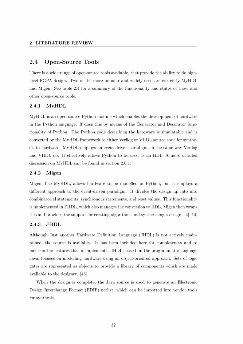
2. LITERATURE REVIEW
2.4 Open-Source Tools
There is a wide range of open-source tools available, that provide the ability to do high-
level FGPA design. Two of the more popular and widely-used are currently MyHDL
and Migen. See table 2.4 for a summary of the functionality and states of these and
other open-source tools.
2.4.1 MyHDL
MyHDL is an open-source Python module which enables the development of hardware
in the Python language. It does this by means of the Generator and Decorator func-
tionality of Python. The Python code describing the hardware is simulatable and is
converted by the MyHDL framework to either Verilog or VHDL source code for synthe-
sis to hardware. MyHDL employs an event-driven paradigm, in the same way Verilog
and VHDL do. It effectively allows Python to be used as an HDL. A more detailed
discussion on MyHDL can be found in section 2.6.1.
2.4.2 Migen
Migen, like MyHDL, allows hardware to be modelled in Python, but it employs a
different approach to the event-driven paradigm. It divides the design up into into
combinatorial statements, synchronous statements, and reset values. This functionality
is implemented in FHDL, which also manages the conversion to HDL, Migen then wraps
this and provides the support for creating algorithms and synthesising a design. [4] [14]
2.4.3 JHDL
Although Just another Hardware Definition Language (JHDL) is not actively main-
tained, the source is available. It has been included here for completeness and to
mention the features that it implements. JHDL, based on the programmatic language
Java, focuses on modelling hardware using an object-oriented approach. Sets of logic
gates are represented as objects to provide a library of components which are made
available to the designer. [43]
When the design is complete, the Java source is used to generate an Electronic
Design Interchange Format (EDIF) netlist, which can be imported into vendor tools
for synthesis.
32
2.5 CASPER Tools
JHDL has some notable features including, a graphical schematic interface, a mul-
tiple clock domain simulator, table-generated state machines and a command line in-
terface. There is no longer active development on the JHDL tools.
2.4.4 Chisel
Constructing Hardware In a Scala Embedded Language (Chisel), developed at The Uni-
versity of California, Berkeley, is a hardware development language that uses highly
parameterised generators and layered hardware DSLs to support advanced hardware
design. Chisel raises the level of abstraction of hardware design by providing an object-
orientation and parameterised types. Chisel generates C++ for cycle-accurate simula-
tion and Verilog to pass to hardware synthesisers. [24] [25]
2.5 CASPER Tools
The primary goal of Collaboration for Astronomy and Signal Processing and Electronic
Research (CASPER) is to provide a streamlined and simple approach to designing radio
astronomy instrumentation, by promoting design reuse and through the development
of open-source hardware and software. The collaboration has designed multiple FPGA
boards, the latest being the ROACH and ROACH2 platforms, based on the Xilinx
Virtex series of FPGA devices.
The current CASPER tool-flow uses Matlab, Simulink and the Xilinx System Gen-
erator (XSG) to provide an environment in which to graphically model DSP systems.
CASPER has put together a set of libraries which implement astronomy-specific DSP
functions on the CASPER hardware platforms, for example, Wideband FFTs and PFB.
There is also a library of controllers which provide interfaces to Analog to Digital Con-
verters (ADC), Random Access Memories (RAM) and Ethernet Controllers. These
libraries and environment allow application developers to quickly and easily create as-
tronomy instruments with little knowledge of the underlying hardware implementation.
This is key, as in the majority of designers are not well-versed in the intricacies of the
FPGA hardware.
2.5.1 Xilinx Tools
All FPGA vendors provide a suite of tools in which to design applications for their
particular FPGA devices. These usually consist of a schematic editor, HDL Integrated
Development Environments (IDE), simulation environments, and manual place and
33
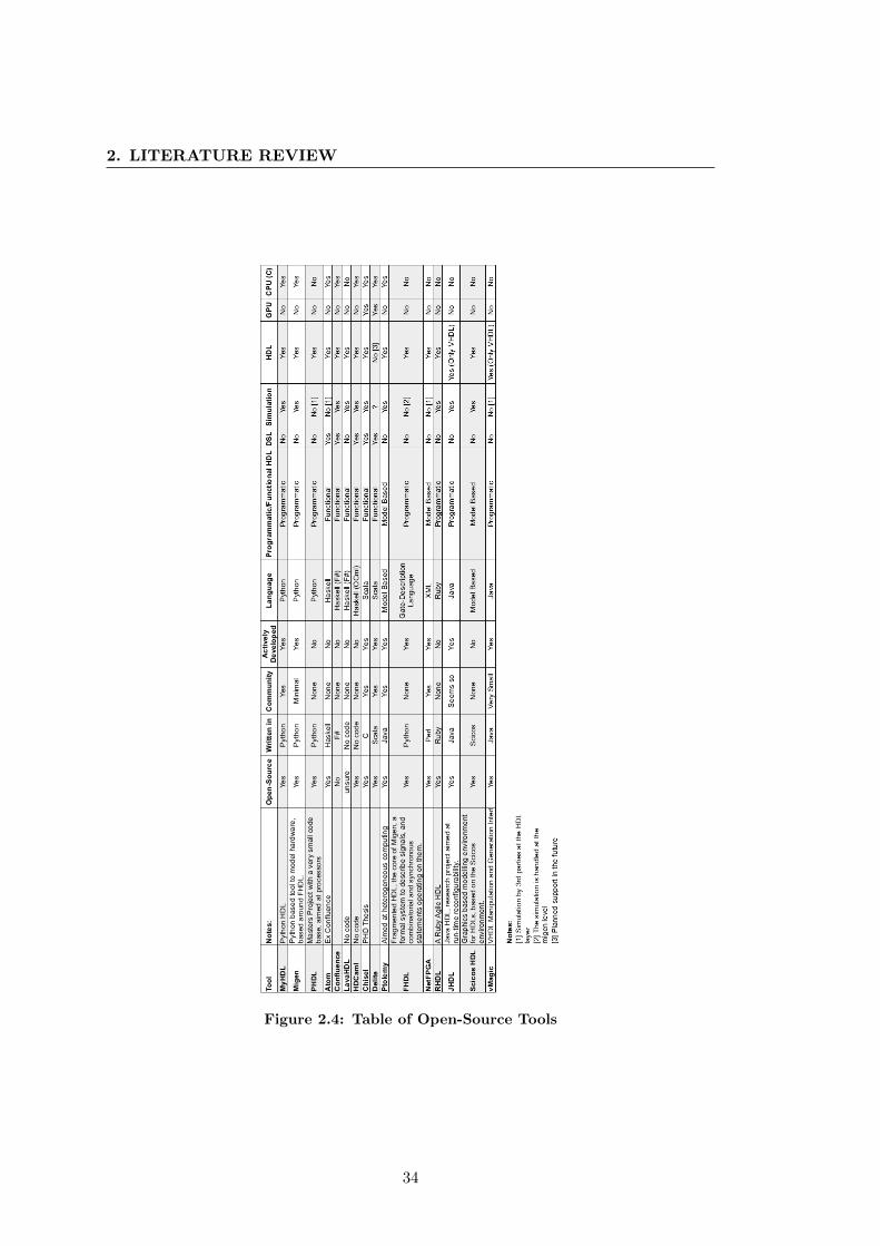
2. LITERATURE REVIEW
Figure 2.4: Table of Open-Source Tools
34

2.5 CASPER Tools
route tools, amongst others. Quartus is Altera’s suite of tools and Xilinx’s software is
the Integrated Synthesis Environment (ISE) and more recently Vivado.
The Vivado Design Suit provides a far more integrated development environment
where the design and build processes integrate more seamlessly. This was a complete
re-architecture of the old ISE tools which struggled with placing and routing designs for
large FGPAs, in particular the Virtex 6 series. Unfortunately Vivado does not support
the 6 series of FPGAs, but only the 7 series upwards. That being said, Vivado is a very
necessary upgrade to the tools and makes designing for FPGAs easier.
Often these tools do not always allow the designer to use the methodology required.
Hence, the vendor tools are often supplemented with third party software, which at-
tempts to ease the development process. Applications such as Labview and Mathworks’
HDL Coder still plug into vendor tools, but abstract the design process to a higher level
block diagram design. Although, Xilinx has released its HLS tool which allows designers
to develop hardware in C, C++ and SystemC.
2.5.1.1 Xilinx System Generator
XSG is a plug-in to the Matlab Simulink environment which provides a Xilinx block set
that can be used in combination with Simulink blocks to design, verify and simulate a
Xilinx FPGA application.
2.5.2 Matlab and Simulink
Simulink is a tool included as part of Matlab that provides an interactive graphical
design environment for a range of model-based applications, including DSP system
design. Simulink also includes a few libraries of blocks which can be included into the
design to inject data into a system to aid in simulation and verification. [9]
The Matlab environment further provides the powerful scripting ability of Matlab
to the designer to aid in testing, verification and simulation.
2.5.3 Libraries
A major part of the CASPER tools are the libraries that can be used in a Simulink
design. Many of these libraries are designed for radio astronomy instrumentation, as
this is the main focus of the collaboration, but often have application in other industries.
[45]
35

2. LITERATURE REVIEW
Figure 2.5: CASPER Design Environment A basic CASPER design that acquires
data via an ADC and stores it in a BRAM
36

2.5 CASPER Tools
Figure 2.6: Xilinx Libraries The Xilinx libraries that can be used in a Simulink design
37

2. LITERATURE REVIEW
2.5.3.1 Yellow Blocks
A Yellow Block is a peripheral controller block that consist of HDL or generated IP
cores that are wrapped with Matlab scripts to enable them to be used in Simulink
designs. The scripts let Simulink and XSG know how the block interacts with the rest
of the design so that it can be correctly connected into the design.
2.5.3.2 Green Blocks
Green blocks are DSPs library block that are generally created from Xilinx primitives
and built up to perform a particular function. The success of these DSP library blocks
is due to the fact that they are parameterised to give them flexibility. Many blocks have
an option to specify the number of parallel inputs. The Matlab scripts then redraw the
underlying structure to fit the specified parameters. [45]
2.5.3.3 Base Projects
For each supported hardware platform, the CASPER tools provide a base project into
which the DSP design is embedded. This is a Xilinx EDK project which contains the
underlying bus architecture and clocking infrastructure required for the design.
2.5.4 Framework
The CASPER framework consists of a set of Matlab scripts which pull the Simulink
design and the base project together. A netlist is generated from the Simulink de-
sign using System Generator. The netlist is then instantiated in an ISE project and
the controllers and peripherals instantiated and connected to the design netlist. The
framework also manages the clocks, for example, when the clock rate is selected the
scripts will configure the clocking infrastructure in such a way as to provide the correct
clock rate. The scripts manage the devices on the memory-mapped bus, allocating
memory to each device and also creating new levels on the bus if the number of devices
gets too high. See section 4.3.1 for a more detailed discussion on the bus infrastructure.
2.5.5 Simulation
Simulating a design is a very important process. This is particularly important due to
the long compile times inherent in FPGA design, which makes it a timely process to
build and test on hardware. It is very useful to understand how particular logic behaves
and interacts with other parts of the design without having to compile and deploy on
hardware.
38
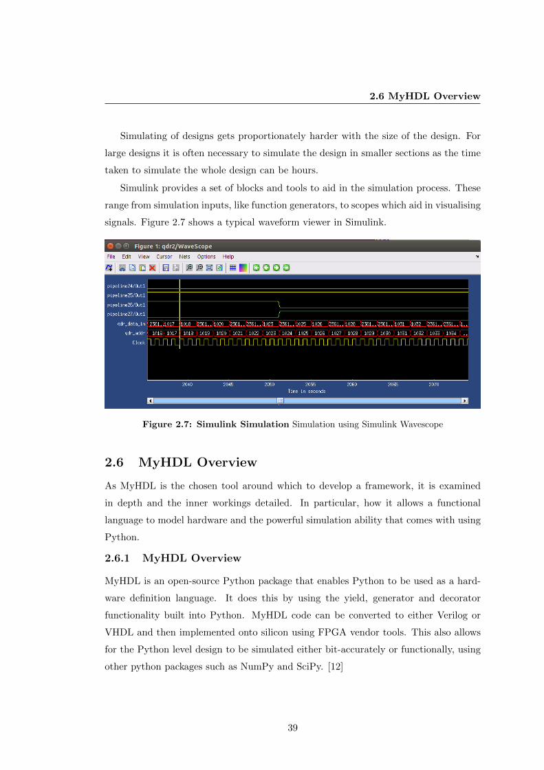
2.6 MyHDL Overview
Simulating of designs gets proportionately harder with the size of the design. For
large designs it is often necessary to simulate the design in smaller sections as the time
taken to simulate the whole design can be hours.
Simulink provides a set of blocks and tools to aid in the simulation process. These
range from simulation inputs, like function generators, to scopes which aid in visualising
signals. Figure 2.7 shows a typical waveform viewer in Simulink.
Figure 2.7: Simulink Simulation Simulation using Simulink Wavescope
2.6 MyHDL Overview
As MyHDL is the chosen tool around which to develop a framework, it is examined
in depth and the inner workings detailed. In particular, how it allows a functional
language to model hardware and the powerful simulation ability that comes with using
Python.
2.6.1 MyHDL Overview
MyHDL is an open-source Python package that enables Python to be used as a hard-
ware definition language. It does this by using the yield, generator and decorator
functionality built into Python. MyHDL code can be converted to either Verilog or
VHDL and then implemented onto silicon using FPGA vendor tools. This also allows
for the Python level design to be simulated either bit-accurately or functionally, using
other python packages such as NumPy and SciPy. [12]
39
2. LITERATURE REVIEW
By using Python, MyHDL provides a high-level language in which to design and
simulate. This eases the hardware verification process and reduces design time. Python
brings with it the flexibility of an interpreted language and the ability to write succinct
and compact code. [46]
2.6.2 Modelling Parallel Hardware with Python
The mindset when designing hardware is very different to that of software development,
primarily due to the fact that FPGAs run many parts of a design concurrently. The
current bottleneck on CPUs is the clock speed, which is forcing a move towards more
parallelised design. This is why the number of cores in CPUs is currently increasing.
This is starting a change in the way that software designers are required to think about
implementation, but a CPU is only a lightly parallel system. FPGAs on the other hand
are highly parallelised, or concurrent, and require a completely different understanding
and approach to design. [20]
For instance, in a programmatic software language, the statements below would be
run sequentially. Assuming a = 1 and b = 3, the outcome on a CPU would be that
both a and b = 3. In hardware however, both these statements are run concurrently
so that a and b swap values.
1 a = b
2 b = a
Listing 3: Parallel Statements
To achieve the same result in software, third variable needs to be added, in which
to temporarily store one of the values, as is shown in listing 4.
1 a = b
2 b = temp
3 b = a
Listing 4: Sequential Code
It is this concurrency that needs to be modelled in software. This is where the
python generators, decorators and yields are used.
40

2.6 MyHDL Overview
2.6.2.1 Python Generators and Yields
To understand how yields work in Python, it is required to first understand iterables
and generators. An iterable is any object that can be iterated through, for instance, a
list. Running the following code creates an iterable list called alist. It can be iterated
through and print out each value in turn.
1 >>> alist = [i*i for i in range(3)]
2 >>> for i in alist:
3 ... print(i)
4 0
5 1
6 4
Listing 5: Python List
A Python generator is a type of iterable, but it allows one one iteration through.
This is because it generates the values as required and does not store them, hence it
is called a generator. This makes it ideally suited to the generation of large sets of
data which are required to be accessed only once. This is exactly the functionality that
would be useful in a Python-based simulator allowing the simulator to use less memory
and rather just compute the values that are required.
1 >>> agenerator = (i*i for i in range(3))
2 >>> for i in agenerator:
3 ... print(i)
4 0
5 1
6 4
Listing 6: Python Generator
Listings 5 and 6 show an iterator and a generator respectively. The only difference
between the two examples are the [] and (). In the second example, agenerator cannot
be iterated through again.
41
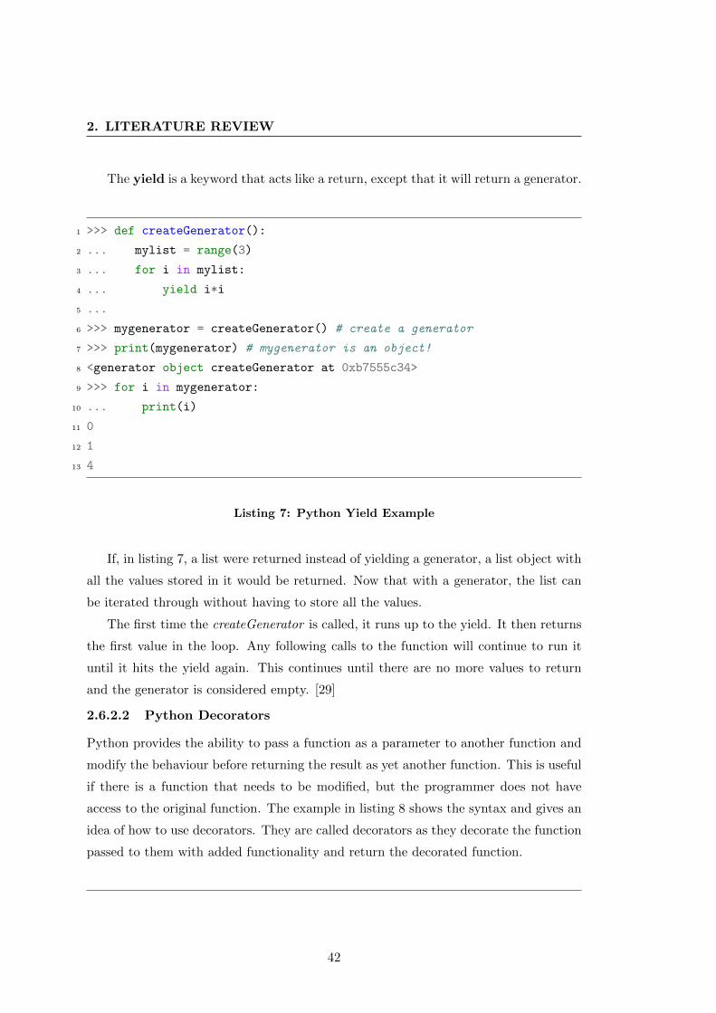
2. LITERATURE REVIEW
The yield is a keyword that acts like a return, except that it will return a generator.
1 >>> def createGenerator():
2 ... mylist = range(3)
3 ... for i in mylist:
4 ... yield i*i
5 ...
6 >>> mygenerator = createGenerator() # create a generator
7 >>> print(mygenerator) # mygenerator is an object!
8 <generator object createGenerator at 0xb7555c34>
9 >>> for i in mygenerator:
10 ... print(i)
11 0
12 1
13 4
Listing 7: Python Yield Example
If, in listing 7, a list were returned instead of yielding a generator, a list object with
all the values stored in it would be returned. Now that with a generator, the list can
be iterated through without having to store all the values.
The first time the createGenerator is called, it runs up to the yield. It then returns
the first value in the loop. Any following calls to the function will continue to run it
until it hits the yield again. This continues until there are no more values to return
and the generator is considered empty. [29]
2.6.2.2 Python Decorators
Python provides the ability to pass a function as a parameter to another function and
modify the behaviour before returning the result as yet another function. This is useful
if there is a function that needs to be modified, but the programmer does not have
access to the original function. The example in listing 8 shows the syntax and gives an
idea of how to use decorators. They are called decorators as they decorate the function
passed to them with added functionality and return the decorated function.
42
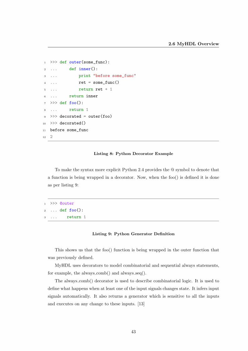
2.6 MyHDL Overview
1 >>> def outer(some_func):
2 ... def inner():
3 ... print "before some_func"
4 ... ret = some_func()
5 ... return ret + 1
6 ... return inner
7 >>> def foo():
8 ... return 1
9 >>> decorated = outer(foo)
10 >>> decorated()
11 before some_func
12 2
Listing 8: Python Decorator Example
To make the syntax more explicit Python 2.4 provides the @ symbol to denote that
a function is being wrapped in a decorator. Now, when the foo() is defined it is done
as per listing 9:
1 >>> @outer
2 ... def foo():
3 ... return 1
Listing 9: Python Generator Definition
This shows us that the foo() function is being wrapped in the outer function that
was previously defined.
MyHDL uses decorators to model combinatorial and sequential always statements,
for example, the always comb() and always seq().
The always comb() decorator is used to describe combinatorial logic. It is used to
define what happens when at least one of the input signals changes state. It infers input
signals automatically. It also returns a generator which is sensitive to all the inputs
and executes on any change to these inputs. [13]
43

2. LITERATURE REVIEW
The always seq() decorator has a limited sensitivity list of either the clock and a
reset or just the clock. It is used as follows:
1 @always_seq(clock.posedge, reset=reset)
Listing 10: MyHDL sequential logic decorator
The decorator automatically infers the reset functionality and detects which signals
need to be reset. The reset signal needs to be a special ResetSignal object to allow for
this functionality. [13]
2.6.2.3 Sensitivity List
HDLs use a sensitivity list to describe event-driven designs or combinatorial logic. A
sensitivity list is a list of wires that trigger an event when any of the listed wire’s
values change. This is especially useful for triggering events on the positive or negative
edges of a clock. Python generators are able to suspend their execution when a yield
statement is encountered. They are resumed again when a specified condition is met.
MyHDL uses this behaviour to model event-driven HDLs in Python and to solve the
issue of concurrency discussed previously. Using decorators, MyHDL is able to specify a
sensitivity list upon which to resume the generate function. The most common MyHDL
decorator function is the @always(event1, event2, ...). [13]
2.6.2.4 Python-Verilog Comparison
The structure of MyHDL is very similar to that of Verilog, particularly because MyHDL
aims to enable Python to be used as an HDL and they are both based on an event-
driven paradigm. The following examples of counters in MyHDL and Verilog show the
similarity.
1 always @(posedge clk) begin
2 if (!rst && out < COUNT_TO) begin
3 if (en == 1) begin
4 out <= out + STEP;
5 end
6 end else begin
44

2.6 MyHDL Overview
7 out <= COUNT_FROM;
8 end
9 end
Listing 11: Verilog Counter Implementation
1 @always(clk.posedge)
2 def logic():
3 if (rst == 0 and out < COUNT_TO):
4 if (en == 1):
5 out = out + STEP
6 else:
7 out = COUNT_FROM
8
9 return logic‘
Listing 12: Python Counter Implementation
2.6.3 MyHDL Types
When modelling hardware there is a need for appropriate types to represent the data
in the system. Ultimately the data is just string of bits but it is very useful to leverage
a type. The built-in type is the integer bit-vector (intbv). The other major type is the
fixed-point bit-vector (fixbv) This is distributed as an additional Python package and
is not incorporated into the MyHDL package yet. These types provide an easier way
of managing arrays of signals and ensure that boundary conditions of the signals are
met.
2.6.4 Simulation
The success of a tool is very much dependent on its ability to simulate a design. This
is where MyHDL features strongly. The integration with Python allows the designers
all the features and tools available in Python to verify and simulate a design. MyHDL
designs can be stimulated and verify very easily using Python toolboxes such as Numpy
45

2. LITERATURE REVIEW
and Scipy. For instance, to test a MyHDL filter the design can be simulated using a
Numpy generated sinusoidal waveform and compare the output with an output from a
Python filter. It is then a simple step to plot the results of a simulation using one of
Python’s plotting libraries. See figure 2.8.
Figure 2.8: Stimulus and Output Simulation input and output of a MyHDL FFT
2.6.5 Co-simulation
The ability to simulate at the higher level is critical, but HDL simulation still needs to
be supported. Once testbenches are written for the higher-level python implementation,
MyHDL provides a means of reusing these testbenches to test and verify the generated
HDL or even the hardware. MyHDL provides this ability for Verilog using the Verilog
Procedural Interface (VPI) which exposes an interface to the Verilog source.
The VPI, originally known as Procedural Language Interface (PLI) 2.0, allows be-
havioural Verilog to invoke C functions, and C functions to invoke standard Verilog
46

2.6 MyHDL Overview
system tasks. [26] The VPI is part of the Verilog specification as set out in IEEE
1364-2008 standard. [33]
When MyHDL generates HDL it also generates an accompanying test bench. The
VPI interface can be specified in this testbench as shown in the following example. If
the ’define MyHDL is defined, then the VPI is used to connect the specified ports clk,
en, rst and out which can now be read and written from the Python testbench. If
MyHDL is not defined, then the standard Verilog testbench is run.
1 ‘ifdef MYHDL
2 // define what myhdl takes over
3 // only if we’re running myhdl
4 initial begin
5 $from_myhdl(clk, en, rst);
6 $to_myhdl(out);
7 end
8 ‘else
9 ...
Listing 13: VPI interface from Python to Verilog
2.6.6 Conversion to HDL
As has been discussed previously, any tool that aids FPGA designs will need to convert
the design into either HDL or Verilog for synthesis by the vendor’s tools. MyHDL
provides functions to convert a design to either language.
1 #=======================================
2 # For testing of conversion to verilog
3 #=======================================
4 def convert():
5
6 clk, en, rst = [Signal(bool(0)) for i in range(3)]
7 out = Signal(intbv(0)[8:])
8
9 toVerilog(counter, clk=clk, en=en, rst=rst, out=out)
47

2. LITERATURE REVIEW
Listing 14: MyHDL code to convert a counter module to Verilog
The example in listing 14 shows how a counter module is converted to Verilog. The
toVerilog() function takes the counter function and the inputs and outputs as parame-
ters. The input and output signals are declared beforehand so that the conversion logic
knows how many bits wide each of the signals is before generating the HDL.
2.6.7 User-Defined Code
MyHDL provides a method of incorporating existing HDL code into a MyHDL design.
This is particularly useful when a designer is migrating existing code to MyHDL, for
example, a Verilog FFT.
1 counter_wrapper.verilog_code = \
2 """
3 counter
4 #(
5 .DATA_WIDTH (£DATA_WIDTH),
6 .COUNT_FROM (£COUNT_FROM),
7 .STEP (£STEP)
8 ) counter_£block_name (
9 .clk (£clk),
10 .en (£en),
11 .rst (£rst),
12 .out (£out)
13 );
14 """
Listing 15: MyHDL User Defined Code
In the example in listing 15 the string verilog code is set to a counter module
instantiation. When a conversion method is run on this module, the code looks for
either a verilog code or vhdl code string. If either exists, then the MyHDL is not
48

2.6 MyHDL Overview
converted directly, but the string is used. The string does not have to be a module
instantiation, but could be an explicit HDL circuit description.
2.6.8 MyHDL Summary
MyHDL allows the features of the Python language to be used in simulation and veri-
fication, which is a powerful tool. Ultimately, MyHDL is a good tool around which to
base a full design-flow.
49

2. LITERATURE REVIEW
50

Chapter 3
Methodology
This chapter details the steps taken to achieving the objectives laid out in section
1.3. This includes: the initial constraints, requirements gathering and requirements
distillation.
3.1 Approach to Achieving the Objectives
The overarching requirement is examined. This is to: evaluate MyHDL as an open-
source tool around which a framework can be created to aid in designing Field Pro-
grammable Gate Array-based (FPGA) Digital Signal Processing (DSP) systems for
radio astronomy instrumentation.
The means of testing is decided on. The tool-flow will be tested by creating example
designs to test specific functionality. The areas that will be tested are the incorporation
of vendor tools, memory-mapped bus creation and simulation of a DSP design. The
analysis of certain metrics, such as ease of use and development time, is also used to
test the success of the tool-flow.
The constraints and assumptions are noted and considered in the subsequent steps.
As with any project, there are limitations and constraints. The two major constraints
for this project are that MyHDL is the tool to be used and that the architecture of the
current CASPER tools is used.
The next step is to gather detailed requirements for the new tool-flow. These are
collected from sources such as the CASPER mailing list, DSP engineers working on
MeerKAT and discussions held at the annual CASPER workshops.
51
3. METHODOLOGY
The gathered requirements is a list of useful features, but needs to be distilled into
workable requirements and then into a design specification.
Due to the scope of this project, only select requirements are implemented. These
requirements are selected carefully, so as to focus on particular key areas. It is important
that these areas are shown to work correctly as they are fundamental to the tool-flow
being a success. These requirements are discussed in detail.
The selected requirements are then designed and implemented. This process, the
problems encountered and the solutions are discussed and explained.
To test particular aspects of the tool-flow, example designs are created. These
target the key areas of the tool-flow and help to gauge the success of the tool-flow.
Each of the example designs is simulated to ensure that it functions as expected.
The simulations for each design are analysed and explained.
The example designs are compiled and deployed on hardware. They are run with
the same stimuli as the simulations and the outputs again analysed and discussed.
It is important to compare the simulation results with the hardware results. This
gives a clear picture of the accuracy of the simulations and allows the success of the
tool-flow to be gauged.
The results of the test designs are analysed and used to measure to what extent the
objectives are met. The metrics established prior to the design of the tool-flow are mea-
sured and discussed. The implemented features are evaluated against the requirements
and the overall success of the project determined.
3.2 Constraints and Assumptions
This project is not undertaken in isolation and there are a number of assumptions
taken before any design work is done. These assumptions serve to limit the scope of
the project and to allow the author to use familiar technologies.
3.2.1 Python as the Modelling Language
The modelling language to be used is Python. Python combines the flexibility of a
scripted language and provides a comprehensive set of mathematical libraries. There
are ideal to be used for simulation and verification. Many users have a background in
Python and this allows for a smoother transition to using the new tool-flow. Python is
ideally suited to integrating the sections of the tool-flow together as well as performing
the simulations and verification tasks.
52

3.2 Constraints and Assumptions
3.2.2 MyHDL as the Framework
MyHDL, a Python-based Hardware Definition Language (HDL), is a proven framework
for FPGA design. Thus, it has been chosen as the framework around which to design
the tool-flow. MyHDL ultimately encompasses the features required for the tool-flow.
See section 2.6.1 for more details. The aim of the project is to evaluate the feasibility of
MyHDL as a framework around which to design an open-source tool-flow for CASPER.
3.2.3 Include Existing HDL Components
It is essential that existing HDL components can be used in the tool-flow. This allows
for simpler migration of existing HDL code into the tool-flow.
3.2.4 Use the Current CASPER Tools Architecture
The current CASPER tools are based on an architecture which consists of a set of
libraries, a base project (per hardware platform) and a framework of scripts. This
architecture has been proven to work well and is the model around which the new tool-
flow is designed. Users are already familiar with this architecture. For these reasons
the new tool-flow is designed to use a similar architecture.
The set of Libraries includes DSP libraries, controller libraries and primitive li-
braries. Any of which can be used in a design. The DSP libraries are built up of
combinations of the primitive libraries. See section 3.1 for more details.
The base project provides the clocking, reset and memory-mapped bus infras-
tructure to the design and is specific to each supported hardware platform. It is the
design into which the DSP is incorporated and connected to.
The framework is the set of scripts which manages the integration of the design
with the base package before compilation. It manages the simulation and verifications
and ultimately calls the vendor tools for synthesis, place and route, map and bit file
generation. See section 3.3 for a detailed overview of the framework.
Before any project is undertaken, it is important to examine the requirements. This
chapter lays out the requirements for the tool-flow and explains how they are gathered.
It looks at the process taken to arrive at the specifications. It also details how the
tool-flow is to be tested and against what criteria the implementation can be declare
successful. This chapter focuses on the major functionality of the tool and breaks it
down into the different subsections required.
53
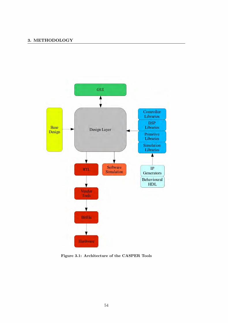
3. METHODOLOGY
Figure 3.1: Architecture of the CASPER Tools
54

3.3 System Engineering and Waterfall Methodologies
The design specification section focuses on the subset of the requirements which are
implemented for this thesis. The tool-flow in its entirety is too large a project to handle
in one masters thesis and therefore, only a selection of the requirements are examined,
designed and implemented. As explained in section 1.6.
3.3 System Engineering and Waterfall Methodologies
As discussed in section 1.5.1, a combination of the System Engineering approach and
the Waterfall methodologies are used to design and implement the tool-flow. The
following steps map the Waterfall methodology and incorporate the steps taken in this
project to assess the viability of a Python-based tool-flow. [59]
The system engineering methodology is a method of managing a large project from
the requirements gathering state through to completion and delivery of a final product.
The system engineering selected steps followed here pertain to this project and its
context.
Figure 3.2: Model of the Waterfall Design Methodology [59]
The System Engineering and Software Design processes take the following steps:
55
3. METHODOLOGY
Step 1: Requirements gathering
Step 2: Analysis of the requirements
Step 3: Creation of the design specification
Step 4: Implementation of the tool-flow
Step 5: Implementation testing
Step 6: Creation of proof-of-concept designs
Step 7: Comparing the proof-of-concept designs against predefined success met-
rics
For a more detailed description of these steps see section 1.5.1.
3.4 Requirements and Analysis
This sections examines the requirements that have been gathered. It divides these
requirements into two sections: the functional and non-functional requirements.
The majority of the user requirements are gathered from the current users of the
CASPER Tool-flow. The requirements are extracted chiefly from discussions held at
previous CASPER Conferences, the experiences of colleagues who work with the current
tools on a daily basis and CASPER mailing-list e-mails. From this, came a range of
requirements, many of which are similar to the current tools. Other requirements stem
from functionality that would make users’ lives easier and save time.
As the design of a tool-flow like this is large and complex, and is beyond the scope
of this project, only a specially selected subset of the requirements are implemented.
3.4.1 High-Level Requirements
Before drilling down into the fine-grained requirements, it is important to understand
the overarching requirements and design goals. Especially during the design and im-
plementation stages. The following requirements are higher-level requirements which
are further broken up into sub requirements that are used to create the Design Speci-
fication.
56
3.4 Requirements and Analysis
The overarching requirement is to:
Design an open-source, Python-based, DSP development framework to target
FPGA-based hardware. To provide an easy-to-use design-flow allowing for rapid
development cycles, using a high-level modelling language to provide verifica-
tion and simulation functionality. Particularly aimed at Software Defined Radio
(SDR) in the fields of radio astronomy and radar. The framework will enable the
design of new Intellectual Property (IP) and provide a mechanism by which to
easily share this IP.
3.4.2 Non-Functional Requirements
The non-functional requirements describe how a system is to operate, as opposed to
describing particular functions of the system. To gauge the success implementation of a
non-functional requirement, it is helpful to make use of a metric which is not necessarily
quantifiable and can be subjective. For example, a requirement to, make it easier to
design for DSP for FPGAs, is a very loosely constrained requirement and is certainly
subjective. The measure of the ease of use differs from one user to another and this
makes it hard to analyse the success of these requirements. While being hard to gauge,
these requirements are still critical to the design of the tools.
• Reduce the time taken to create DSP systems.
To manage this, an application designer needs to design at a higher level than
the HDL, as the complexities of FPGAs often distract from the main focus, to
implement a design. A better method would be to let expert FPGA designers
create sets of libraries that application designers can use in their designs.
• Use a model integrated development methodology.
The Model-Driven Development (MDD) methodology ensures rapid development
cycles and makes it easy to reuse previous work. This comes with its drawbacks
and needs to be implemented carefully. See section 2.2.4 for an in-depth discussion
of MDD.
57

3. METHODOLOGY
• Provide a high level of stability.
The current CASPER tools, using Matlab/Simulink and Xilinx System Genera-
tor, have been unstable. This is particularly when compiling larger designs. With
compilations taking in the order of hours, instabilities can be costly.
The metrics used to evaluate the above non-functional requirements are listed below.
They are examined in the final chapter of this work in order to gauge to what extent
they are met.
• How easy is it to learn the new tool-flow compared to the previous tool-flow?
This is expected to be similar, as the MDD methodology is used for both tools.
• How long does it take to create a design in the new tool-flow? Is this more or less
than the previous tool-flow?
• How stable is the new tool-flow? The previous tool-flow often froze or stalled
during compilation. Is the new tool-flow an improvement?
3.4.3 Functional Requirements
The functional requirements of the system are split up into four major sections: general
requirements, library requirements, framework requirements and base project require-
ments. Many of the requirements span multiple sections. For example, parts of the bus
infrastructure are implemented in the base project, the framework and the libraries.
Figure 3.3 describes the full architecture and design of the tool-flow.
3.4.3.1 General Requirements
• Framework must be able to target both Xilinx and Altera FPGAs.
This requires integration of both Quartus and Integrated Synthesis Environment
(ISE) tools. This is important as it will allow designers to share IP and designs
across platforms. This keeps the DSP section of a design hardware independent.
So that it is required to replace only the peripherals when changing platform.
• Support for Windows and Linux operating systems.
The framework must be able to run on both Windows and Linux as these are both
supported by the vendor (Xilinx and Altera) tools. This can be accomplished by
writing the framework of the tool-flow in a language such as Python.
58

3.4 Requirements and Analysis
Figure 3.3: Full Architecture of the Tool-flow
59
3. METHODOLOGY
• Provide a one-click solution to compile a design to a bitstream.
This is to abstract the designer away from the vendor tools or underlying frame-
work and allows the focus to be on creating the DSP application.
• Provide the functionality to model, simulate and verify designs using
a high-level language.
The ability of a tool-flow to simulate designs is a key function. This is best
achieved in a higher level language. The MyHDL project brings this functionality.
• Provide a set of parameterised libraries.
To facilitate with the design of DSP systems, a set of highly parameterised li-
braries is needed. This promotes the reuse of modules and aids in the rapid
implementation of systems. The libraries will cover the following categories: con-
trollers, primitives and DSP. The designer must be able to easily create any
modules which do not exist and add them to the libraries.
• Support multiple hardware platforms.
The tool-flow needs to allow the application engineer to reuse as much work as
possible, particularly the DSP sections of the design. To accomplish this, the
framework needs to know about each supported hardware platform, from its pin
mappings to its supported controllers. The libraries will need to be designed
in such a way as to accommodate for this by linking platforms and supported
controllers.
• Flexible blocks using parameterisation and redrawing.
The key to the success of the CASPER tools is the ability to redraw blocks and
change the number of Input/Output (I/O) ports when a parameter is changed.
This is not possible to do in pure HDL as the ports on a module are fixed and
require an intermediate or high-level language to manage this.
• Provide a streamlined solution from design to bitstream.
There are many steps taken in the process to get from a top-level design to bit-
stream that can be uploaded onto an FPGA. This process involves logic synthesis,
place and route, mapping and bit generation. Ideally, this could be abstracted
60

3.4 Requirements and Analysis
away from the designer. Unfortunately, due to the nature of the FPGAs, a de-
signer requires a good understanding of how the technology implements a design
to be able to optimise for efficiency. This means that, while a one-click design to
bitstream is required, all the options for the synthesis, place and route, map and
bit generation are made available to the designer.
• Provide a Graphical User Interface (GUI).
The success of the current CASPER tools can be largely attributed to the GUI
that Matlab/Simulink provides. It is imperative for the adoption of this tool that
it has an intuitive interface in which users can manipulate designs. While this is
a requirement, the implementation is outside of the scope this project.
3.4.3.2 Libraries
The libraries need to provide the majority of the blocks that an application designer
would require, from simple primitive multipliers to more complex Fast Fourier Trans-
forms (FFT). It will also provide the functionality to create new blocks that can be
added to the existing libraries.
It is of particular importance to provide a set of radio astronomy-specific libraries
which are tailored to the type of processing required in Radio Astronomy DSP systems,
such as wideband FFTs and Polyphase Filter Banks (PFB)
• Primitive Library
The primitive library provides a comprehensive set of primitives, which includes
multipliers, adders and vendor primitives, such as, DSP slices and Look Up Tables
(LUT). Each module supplies a behavioural HDL model and a Python model for
simulation.
• Controller Library
The controller library provides a set of peripheral controllers for each hardware
platform supported. These will differ for each hardware platform, although some
may be shared across platforms. Example controllers are: Quad Data Rate
(QDR) memory, Analog to Digital Converters (ADC) and Dynamic Random
Access Memory (DRAM).
61
3. METHODOLOGY
• DSP Library
The DSP library provides a set of DSP blocks which are made up of combinations
of primitives. New DSP modules can easily be created from existing modules
and incorporated into the libraries. The framework provides a way to script the
connections and sub-blocks within the DSP blocks. This will serve to provide a
high level of flexibility. This is also a function of the framework.
• Automatic IP Core Generation
The tool-flow will also provide the ability to include vendor specific IP cores into
a design. These are generated at compile time, as storing or distributing the
generated IP would be in breach of licensing agreements. This reduces the porta-
bility of designs to similar FPGA devices. Although, the tools would incorporate
a mechanism where by the targeted FPGA’s IP can be incorporated dynamically.
3.4.3.3 Framework
The design-flow is the core of the tools, it manages the entire flow, from the design
rules check to the bit file generation. It takes the DSP design file and integrates it with
the correct base project and integrates the controller cores, buses and clocks. It also
provides the functionality to redraw blocks, depending on the module’s configuration
parameters.
• design rules check
The framework is responsible for running a Design Rules Check (DRC). This
validates a number of important aspects of the design and serves to catch issues
before the long process of compilation is started. These checks range from ensur-
ing correct bit-widths between modules to ensuring that compatible parameters
have been specified for a particular module.
• Redrawing of blocks
This is one of the key requirements, as it provides the flexibility that is missing
in pure HDL development. By configuring a set of parameters, the entire ar-
chitecture of the block can be redrawn and sub-blocks connected as to meet the
parameter configuration. It can change the number of I/O ports, which is not
possible in pure HDL. See section 4.3.3 for an example.
62

3.4 Requirements and Analysis
• Bus management
The application designer does not need to know about the intricacies of the bus
infrastructure. To abstract the designer from this, the tool-flow automatically
connects the necessary blocks to the bus. This requires a flexible/parameterised
bus controller that can take any number of devices.
• Incorporate vendor tools
Vendor compilation and synthesis tools will need to be integrated into the design-
flow. Ultimately, this will be a one-click solution. Vendors provide an interface
to their tools using Tool Command Language (TCL). It provides the ability to
use flags to control how the tools behave. The framework could construct TCL
scripts and run them to configure and build designs.
• Logging framework
The tool-flow requires a logging framework which will handle the warnings and
errors thrown when generating, compiling and synthesising a design. These logs
are written to corresponding log files.
• Functional verification and bit-accurate simulation
The tool-flow will provide an integrated solution to functionally verify and sim-
ulate the design. This requirement is shared across multiple areas. The libraries
need to provide simulation models and the tool-flow manages the verification and
simulation of these models as well as integrating them into the rest of the design.
It is also possible to integrate Modelsim for additional simulation.
3.4.3.4 Base Projects
A base design is provided for each hardware platform supported. This is a minimalistic
design that includes the clocking and system reset infrastructure, control bus infras-
tructure and the peripheral controllers. The DSP design is pulled into the base design
at compile time to create the final design to be uploaded to the FPGA.
• Base Project Design
To enable support of different hardware platforms the tool-flow needs to pro-
vide base projects for each hardware platform supported. These base projects
63

3. METHODOLOGY
are gateware designs including: clocking infrastructure, bus infrastructure and
supporting HDL), pin constraints and supported gateware peripheral controllers.
• Clock and Bus Infrastructure
The base projects should contain the bus, clocking and reset infrastructure so that
the designer does not have manage this himself. The clock is configurable from
the design, so the mechanism to manage this is included in the base package. In
the case of a Xilinx part this is done via an Multi-Mode Clock Manager (MMCM).
• Pin Mappings
It will also contain the pin mapping and constraints files. The pins included in
the design are dependent on the controllers used and is dynamically included in
the pin constraints file.
• Support for Adding New Hardware
For the tool-flow to be useful it needs to support a wide range of platforms. Thus,
it is key to provide an easy way to add new platforms to the flow. The process
can be eased by providing tutorials and instructions for adding support for new
hardware platforms.
• Controllers
For each base project, a set of supported controllers is included, this requirement
overlaps with the library requirements. When a new base design (hardware plat-
form) is added, all the supporting controllers need to be added to the controller
library. This includes all peripherals available on the hardware, which could in-
clude QDR, DRAM ADCs, Ethernet and more.
3.5 Conclusions
The discussed requirements and constraint provide a very good starting point for the de-
velopment of the tool-flow. The architecture of the tools remains largely the same. The
methodologies to be implemented have been tested and proven in the current CASPER
tool-flow and other projects. The tool-flow is implemented using these requirements
in the following chapter. It details the design process, how certain requirements are
implemented and the challenges and solutions to them.
64

Chapter 4
Design and Implementation
This section deals with the design and implementation of the requirements laid out in
the previous section. It explains how aspects of the tool-flow are implemented to meet
the requirements. Due to the extensive amount of work to implement the full tool-flow,
only certain parts of the tool-flow are implemented. The main focus is on the libraries,
framework and base projects.
There are a number of high-level design decisions that are taken. Firstly, the tool-
flow structure is split up into four distinct sections: Graphical User Interface (GUI),
Framework, Libraries and Base Projects. Although each part brings different func-
tionality to the tool-flow, they are not mutually exclusive. For instance, much of the
functionality of the Digital Signal Processing (DSP) library blocks span the framework
and the libraries.
The infrastructure around which to design the tool-flow was a major decision. Af-
ter researching open-source Field Programmable Gate Array (FPGA) tools and frame-
works, MyHDL was the best tool with which to to do this. It provides the functionality
to model and verify FPGA designs in Python. See section 2.4 Python is also a script-
ing language and this aligns perfectly with the requirement to be able to script the
redrawing of DSP blocks along with other aspects of the tool-flow. See section 6.2.2.2
for details of block redrawing.
The design-flow will consist of a number of distinct sections that interact with each
other. Each brings a unique aspect to the flow, although some functionality may be
split across these sections where necessary.
The areas focused on are:
65
4. DESIGN AND IMPLEMENTATION
• An overarching design specification
• A base project
• Provided libraries
• Bus and clock management frameworks
• Redrawing of the DSP library blocks
• The top-level representation of an application design
• Functional verification and simulation
The three main areas are the libraries, the framework and the base packages. These
sections are clearly distinguishable, but some features are required to be implemented
across two or more of the sections. For example, the memory-mapped bus falls into
all three sections. The framework manages the memory allocation and connects the
memory-mapped bus modules provided in the libraries to those that are in the base
packages. Thus, the same feature may be dealt with in different sections.
The following sections shows how the requirements are taken through to the design
of the tool-flow. The implementation of each requirement is discussed and important
design decisions explained.
4.1 Libraries
For the tool-flow to be useful, it is important that a good set of flexible libraries are
available to the application designer. The way that these blocks are designed is also
important as each block needs to have a Python model that matches the behavioural
Hardware Definition Language (HDL) code exactly.
The libraries are split up into three sets of blocks, DSP blocks, controller blocks
and primitive blocks. The primitive and DSP block sets require Python models that
match the behaviour of the HDL code. This is verified by means of a test bench run
against both the Python and HDL models and the outputs compared.
To facilitate with the design of DSP systems, a set of highly parameterised libraries
has been created, which promotes the reuse of modules and aids in the rapid implemen-
tation of radio astronomy instrumentation designs. These libraries are mostly written
66
4.1 Libraries
in Verilog and wrapped in Python, using MyHDL to provide an easy path to simula-
tion. The libraries are divided into three categories: controllers, primitives and DSP
modules.
These libraries are open-source so that a designer can create or modify the libraries
and share them with the rest of the community. Ultimately this serves to expand the
available libraries.
When designing and implementing libraries, it is important to understand how to
achieve a reasonable amount of flexibility. The following section deals with methods
used to create flexible libraries.
4.1.1 Creating Flexible Libraries
To create a working set of HDL libraries that are flexible and useful, the modules need
to be parameterised in a meaningful and usable way. There are three methods that
can be used to create these flexible modules namely, parameterisation, ’defines and
generate statements. Each of these three methods is tailored to different applications.
For instance, a global, design-wide parameter such as an active-high reset, would be
best implemented as a ’define, whereas a parameter local to a single module, such as
data width, would be implemented as a Verilog parameter.
It is also possible to implement this flexibility at different levels in the tool-flow.
For instance, it can be implemented at the HDL level or, for more complex modules,
at the Python-level. In the general case, the primitives can provide enough flexibility
within the HDL module itself, but for complex DSP modules it is a simpler and almost
necessary to use Python to achieve the required flexibility.
4.1.1.1 Parameterisation
The simplest way to create a flexible and reusable module in Verilog is by making
use of parameters. Parameters are evaluated at compile-time and used to configure
the module accordingly. At a minimum DATA WIDTH parameters should be used to
allow use of the module with data of differing widths. The example below shows how
a counter module parameter can be parameterised to achieve a good level of flexibility.
1 module counter #(
2 //==============================
3 // Top level block parameters
67

4. DESIGN AND IMPLEMENTATION
4 //==============================
5 // number of bits in counter
6 parameter DATA_WIDTH = 8,
7 // provide an enalbe port
8 parameter ENABLE = 1,
9 // start with this number
10 parameter COUNT_FROM = 0,
11 // value to count to in count limited case, defaults to the DATA_WIDTH
12 parameter COUNT_TO = 2^(DATA_WIDTH-1),
13 // negative or positive, sets direction
14 parameter STEP = 1,
15 // should the counter wrap
16 parameter WRAP = 1
17 ) (
18 //===============
19 // Input Ports
20 //===============
21 input clk,
22 input en,
23 input rst,
24
25 //===============
26 // Output Ports
27 //===============
28 output reg [DATA_WIDTH-1:0] out
29 );
30 // Synchronous logic
31 always @(posedge clk) begin
32 // if ACTIVE_LOW_RST is defined then reset on a low
33 // this should be defined on a system-wide basis
34 if ((‘ifdef ACTIVE_LOW_RST rst ‘else !rst ‘endif) && out < COUNT_TO) begin
35 ‘ifdef ENABLE if (en == 1) begin ‘endif
36 out <= out + STEP;
37 ‘ifdef ENABLE end ‘endif
38 end else begin
39 out <= COUNT_FROM;
68
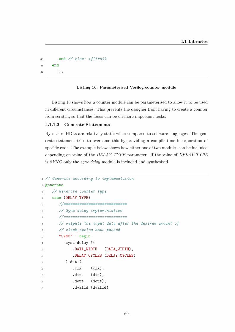
4.1 Libraries
40 end // else: if(!rst)
41 end
42 );
Listing 16: Parameterised Verilog counter module
Listing 16 shows how a counter module can be parameterised to allow it to be used
in different circumstances. This prevents the designer from having to create a counter
from scratch, so that the focus can be on more important tasks.
4.1.1.2 Generate Statements
By nature HDLs are relatively static when compared to software languages. The gen-
erate statement tries to overcome this by providing a compile-time incorporation of
specific code. The example below shows how either one of two modules can be included
depending on value of the DELAY TYPE parameter. If the value of DELAY TYPE
is SYNC only the sync delay module is included and synthesised.
1 // Generate according to implementation
2 generate
3 // Generate counter type
4 case (DELAY_TYPE)
5 //============================
6 // Sync delay implementation
7 //============================
8 // outputs the input data after the desired amount of
9 // clock cycles have passed
10 "SYNC" : begin
11 sync_delay #(
12 .DATA_WIDTH (DATA_WIDTH),
13 .DELAY_CYCLES (DELAY_CYCLES)
14 ) dut (
15 .clk (clk),
16 .din (din),
17 .dout (dout),
18 .dvalid (dvalid)
69
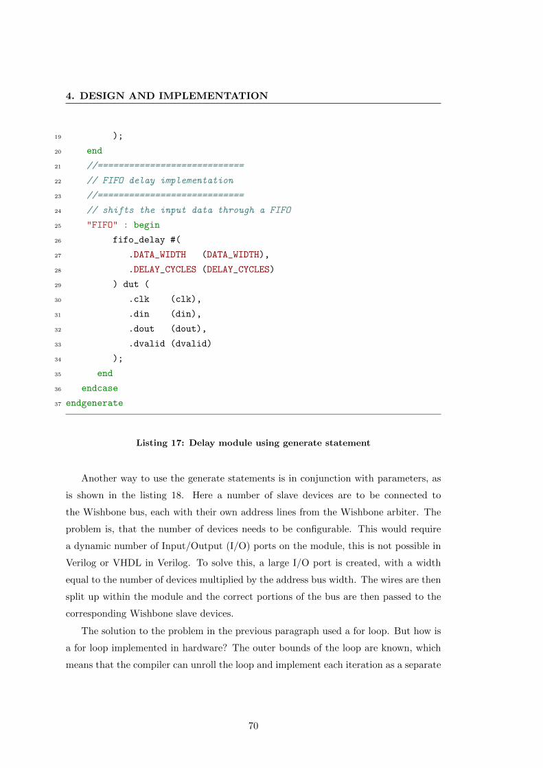
4. DESIGN AND IMPLEMENTATION
19 );
20 end
21 //============================
22 // FIFO delay implementation
23 //============================
24 // shifts the input data through a FIFO
25 "FIFO" : begin
26 fifo_delay #(
27 .DATA_WIDTH (DATA_WIDTH),
28 .DELAY_CYCLES (DELAY_CYCLES)
29 ) dut (
30 .clk (clk),
31 .din (din),
32 .dout (dout),
33 .dvalid (dvalid)
34 );
35 end
36 endcase
37 endgenerate
Listing 17: Delay module using generate statement
Another way to use the generate statements is in conjunction with parameters, as
is shown in the listing 18. Here a number of slave devices are to be connected to
the Wishbone bus, each with their own address lines from the Wishbone arbiter. The
problem is, that the number of devices needs to be configurable. This would require
a dynamic number of Input/Output (I/O) ports on the module, this is not possible in
Verilog or VHDL in Verilog. To solve this, a large I/O port is created, with a width
equal to the number of devices multiplied by the address bus width. The wires are then
split up within the module and the correct portions of the bus are then passed to the
corresponding Wishbone slave devices.
The solution to the problem in the previous paragraph used a for loop. But how is
a for loop implemented in hardware? The outer bounds of the loop are known, which
means that the compiler can unroll the loop and implement each iteration as a separate
70
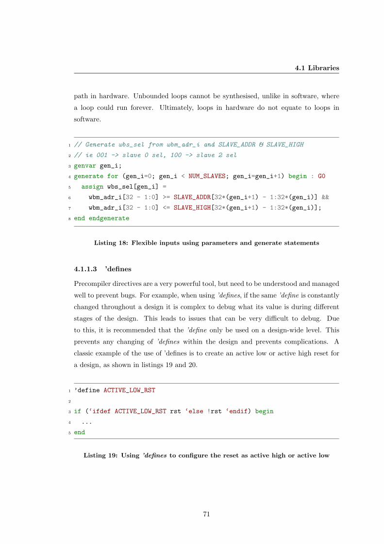
4.1 Libraries
path in hardware. Unbounded loops cannot be synthesised, unlike in software, where
a loop could run forever. Ultimately, loops in hardware do not equate to loops in
software.
1 // Generate wbs_sel from wbm_adr_i and SLAVE_ADDR & SLAVE_HIGH
2 // ie 001 -> slave 0 sel, 100 -> slave 2 sel
3 genvar gen_i;
4 generate for (gen_i=0; gen_i < NUM_SLAVES; gen_i=gen_i+1) begin : G0
5 assign wbs_sel[gen_i] =
6 wbm_adr_i[32 - 1:0] >= SLAVE_ADDR[32*(gen_i+1) - 1:32*(gen_i)] &&
7 wbm_adr_i[32 - 1:0] <= SLAVE_HIGH[32*(gen_i+1) - 1:32*(gen_i)];
8 end endgenerate
Listing 18: Flexible inputs using parameters and generate statements
4.1.1.3 ’defines
Precompiler directives are a very powerful tool, but need to be understood and managed
well to prevent bugs. For example, when using ’defines, if the same ’define is constantly
changed throughout a design it is complex to debug what its value is during different
stages of the design. This leads to issues that can be very difficult to debug. Due
to this, it is recommended that the ’define only be used on a design-wide level. This
prevents any changing of ’defines within the design and prevents complications. A
classic example of the use of ’defines is to create an active low or active high reset for
a design, as shown in listings 19 and 20.
1 ’define ACTIVE_LOW_RST
2
3 if (‘ifdef ACTIVE_LOW_RST rst ‘else !rst ‘endif) begin
4 ...
5 end
Listing 19: Using ’defines to configure the reset as active high or active low
71
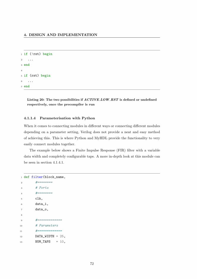
4. DESIGN AND IMPLEMENTATION
1 if (!rst) begin
2 ...
3 end
4
5 if (rst) begin
6 ...
7 end
Listing 20: The two possibilities if ACTIVE LOW RST is defined or undefined
respectively, once the precompiler is run
4.1.1.4 Parameterisation with Python
When it comes to connecting modules in different ways or connecting different modules
depending on a parameter setting, Verilog does not provide a neat and easy method
of achieving this. This is where Python and MyHDL provide the functionality to very
easily connect modules together.
The example below shows a Finite Impulse Response (FIR) filter with a variable
data width and completely configurable taps. A more in-depth look at this module can
be seen in section 4.1.4.1.
1 def filter(block_name,
2 #========
3 # Ports
4 #========
5 clk,
6 data_i,
7 data_o,
8
9 #=============
10 # Parameters
11 #=============
12 DATA_WIDTH = 25,
13 NUM_TAPS = 10,
72
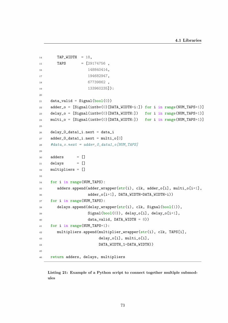
4.1 Libraries
14 TAP_WIDTH = 18,
15 TAPS = [29174756 ,
16 148840414,
17 194682947,
18 67739862 ,
19 133960235]):
20
21 data_valid = Signal(bool(0))
22 adder_o = [Signal(intbv(0)[DATA_WIDTH+i:]) for i in range(NUM_TAPS+1)]
23 delay_o = [Signal(intbv(0)[DATA_WIDTH:]) for i in range(NUM_TAPS+1)]
24 multi_o = [Signal(intbv(0)[DATA_WIDTH:]) for i in range(NUM_TAPS+1)]
25
26 delay_0_data1_i.next = data_i
27 adder_0_data1_i.next = multi_o[0]
28 #data_o.next = adder_0_data1_o[NUM_TAPS]
29
30 adders = []
31 delays = []
32 multipliers = []
33
34 for i in range(NUM_TAPS):
35 adders.append(adder_wrapper(str(i), clk, adder_o[i], multi_o[i+1],
36 adder_o[i+1], DATA_WIDTH=DATA_WIDTH+i))
37 for i in range(NUM_TAPS):
38 delays.append(delay_wrapper(str(i), clk, Signal(bool(1)),
39 Signal(bool(0)), delay_o[i], delay_o[i+1],
40 data_valid, DATA_WIDTH = 8))
41 for i in range(NUM_TAPS+1):
42 multipliers.append(multiplier_wrapper(str(i), clk, TAPS[i],
43 delay_o[i], multi_o[i],
44 DATA_WIDTH_1=DATA_WIDTH))
45
46 return adders, delays, multipliers
Listing 21: Example of a Python script to connect together multiple submod-
ules
73
4. DESIGN AND IMPLEMENTATION
Although this could be achieved using generate statements in the Verilog code, it
is much easier to do with Python. It is simpler and Python constructs lend themselves
to doing this more succinctly, particularly for complex DSP modules.
4.1.2 Primitive Libraries
The primitive library modules are Verilog implementations of low-level modules such
as bit slicers, multiplexers, counters and Block Random Access Memories (BRAM).
These modules are parameterised to an extent that provides coverage of the majority
of the use-cases of the primitive but without creating complexity.
Most FPGA devices have dedicated hardware for particular primitives. For in-
stance, the dual-port block memories, dedicated clock management primitives and DSP
logic elements. These primitives can be instantiated in the same way as a normal mod-
ule, which allows the vendor synthesiser to pull in the corresponding netlist or Register
Transfer Level (RTL).1
4.1.2.1 Vendor Primitives
There is a need to provide the vendor primitives at the Python layer. For Xilinx de-
vices, this includes Intellectual Property (IP) core, DSP Slices, Input/Output Buffers
(IOBufs) and Clock Management Primitives. The DSP slices, although used for DSP
applications, are still a primitive provided by Xilinx. The Python is effectively a wrap-
per around these primitives and exposes the required parameters and configurations
settings. Sometimes simulation logic is provided for the primitive, but in most cases,
the primitives are used in creating a larger module which itself provides a higher-level
simulation model.
In HDL, a vendor primitive is instantiated in the same way any module is in-
stantiated. The synthesiser identifies it as a primitive and inserts the corresponding
IP. In MyHDL this can be done using user-defined code, as the user is incorporating
pre-existing code into a design. Using these library modules would break vendor com-
patibility but in some cases this may be necessary to achieve the optimisations required.
See section 2.6.7 for an example of user-defined code. 2
1Refer to www.github.com/wnew/hdl primitives/2Refer to www.github.com/wnew/hdl vendor primitives/
74

4.1 Libraries
4.1.2.2 Counter Example
A counter is a widely used primitive. It can be used for anything from incrementing
the address lines to keeping track of the number of times an event has occurred.
Here a flexible counter primitive module designed in Verilog and wrapped in Python
is examined. It is simulated and co-simulated and the results compared. This will
provide a good example of how a module can be included into the libraries and give
enough flexibility to be of use to other designers.
The Verilog counter module takes a parameters to provide a reasonable amount
of flexibility, these are DATA WIDTH, COUNT FROM, COUNT TO and STEP. The
default for COUNT TO is the maximum value that can be stored in the DATA WIDTH.
Line 27 of listing 22 shows ’defines being used to allow selection of an active high or
active low reset.
1 module counter #(
2 //==============================
3 // Top level block parameters
4 //==============================
5 parameter DATA_WIDTH = 8, // number of bits in counter
6 parameter COUNT_FROM = 0, // start with this number
7 parameter COUNT_TO = 2^(DATA_WIDTH-1), // value to count to in CL case
8 parameter STEP = 1 // negative or positive, sets direction
9 ) (
10 //===============
11 // Input Ports
12 //===============
13 input clk,
14 input en,
15 input rst,
16
17 //===============
18 // Output Ports
19 //===============
20 output reg [DATA_WIDTH-1:0] out
21 );
75
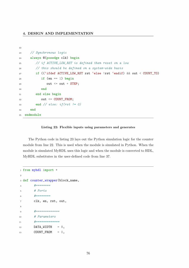
4. DESIGN AND IMPLEMENTATION
22
23 // Synchronous logic
24 always @(posedge clk) begin
25 // if ACTIVE_LOW_RST is defined then reset on a low
26 // this should be defined on a system-wide basis
27 if ((‘ifdef ACTIVE_LOW_RST rst ‘else !rst ‘endif) && out < COUNT_TO)
28 if (en == 1) begin
29 out <= out + STEP;
30 end
31 end else begin
32 out <= COUNT_FROM;
33 end // else: if(rst != 0)
34 end
35 endmodule
Listing 22: Flexible inputs using parameters and generates
The Python code in listing 23 lays out the Python simulation logic for the counter
module from line 22. This is used when the module is simulated in Python. When the
module is simulated MyHDL uses this logic and when the module is converted to HDL,
MyHDL substitutes in the user-defined code from line 37.
1 from myhdl import *
2
3 def counter_wrapper(block_name,
4 #========
5 # Ports
6 #========
7 clk, en, rst, out,
8
9 #=============
10 # Parameters
11 #=============
12 DATA_WIDTH = 8,
13 COUNT_FROM = 0,
76
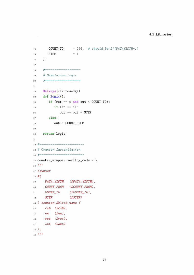
4.1 Libraries
14 COUNT_TO = 256, # should be 2^(DATAWIDTH-1)
15 STEP = 1
16 ):
17
18 #===================
19 # Simulation Logic
20 #===================
21
22 @always(clk.posedge)
23 def logic():
24 if (rst == 0 and out < COUNT_TO):
25 if (en == 1):
26 out == out + STEP
27 else:
28 out = COUNT_FROM
29
30 return logic
31
32 #========================
33 # Counter Instantiation
34 #========================
35 counter_wrapper.verilog_code = \
36 """
37 counter
38 #(
39 .DATA_WIDTH (£DATA_WIDTH),
40 .COUNT_FROM (£COUNT_FROM),
41 .COUNT_TO (£COUNT_TO),
42 .STEP (£STEP)
43 ) counter_£block_name (
44 .clk (£clk),
45 .en (£en),
46 .rst (£rst),
47 .out (£out)
48 );
49 """
77

4. DESIGN AND IMPLEMENTATION
50
51 #=======================================
52 # For testing of conversion to verilog
53 #=======================================
54 def convert():
55
56 clk, en, rst = [Signal(bool(0)) for i in range(3)]
57 out = Signal(intbv(0)[8:])
58
59 toVerilog(counter_wrapper, block_name="cntr2", clk=clk, en=en, rst=rst, out=out)
60
61 if __name__ == "__main__":
62 convert()
Listing 23: MyHDL User-Defined Code used to wrap a counter module
1 module counter_tb;
2
3 //===================
4 // local parameters
5 //===================
6 localparam LOCAL_DATA_WIDTH = ‘ifdef DATA_WIDTH ‘DATA_WIDTH ‘else 8 ‘endif;
7
8 //=============
9 // local regs
10 //=============
11 reg clk;
12 reg en;
13 reg rst;
14
15 //==============
16 // local wires
17 //==============
18 wire [LOCAL_DATA_WIDTH-1:0] out;
78
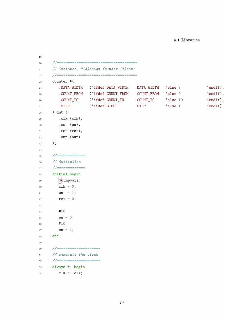
4.1 Libraries
19
20 //=====================================
21 // instance, "(d)esign (u)nder (t)est"
22 //=====================================
23 counter #(
24 .DATA_WIDTH (‘ifdef DATA_WIDTH ‘DATA_WIDTH ‘else 8 ‘endif),
25 .COUNT_FROM (‘ifdef COUNT_FROM ‘COUNT_FROM ‘else 0 ‘endif),
26 .COUNT_TO (‘ifdef COUNT_TO ‘COUNT_TO ‘else 10 ‘endif),
27 .STEP (‘ifdef STEP ‘STEP ‘else 1 ‘endif)
28 ) dut (
29 .clk (clk),
30 .en (en),
31 .rst (rst),
32 .out (out)
33 );
34
35 //=============
36 // initialize
37 //=============
38 initial begin
39 $dumpvars;
40 clk = 0;
41 en = 1;
42 rst = 0;
43
44 #50
45 en = 0;
46 #10
47 en = 1;
48 end
49
50 //====================
51 // simulate the clock
52 //====================
53 always #1 begin
54 clk = ~clk;
79

4. DESIGN AND IMPLEMENTATION
55 end
56
57 //===============
58 // print output
59 //===============
60 always @(posedge clk) $display(out);
61
62 //===============================
63 // finish after 100 clock cycles
64 //===============================
65 initial #100 $finish;
66
67 endmodule
Listing 24: Verilog Counter Test Bench
Listing 25 shows the simulation output from a Verilog test bench which sets COUNT VALUE
to zero, the DATA WIDTH to three and the STEP to one. The output is observed to
wrap when the decimal value increases to seven. This is the expected behaviour, as the
counter is only three bits wide. To ensure that the Python model and the Verilog mod-
ule behave exactly the same, the outputs of both the Python and Verilog simulations
are compared against each other.
1 DATA_WIDTH=3
2 COUNT_FROM=0
3 STEP=1
4
5 Output
6 =============
7 0
8 1
9 2
10 3
11 4
12 5
80
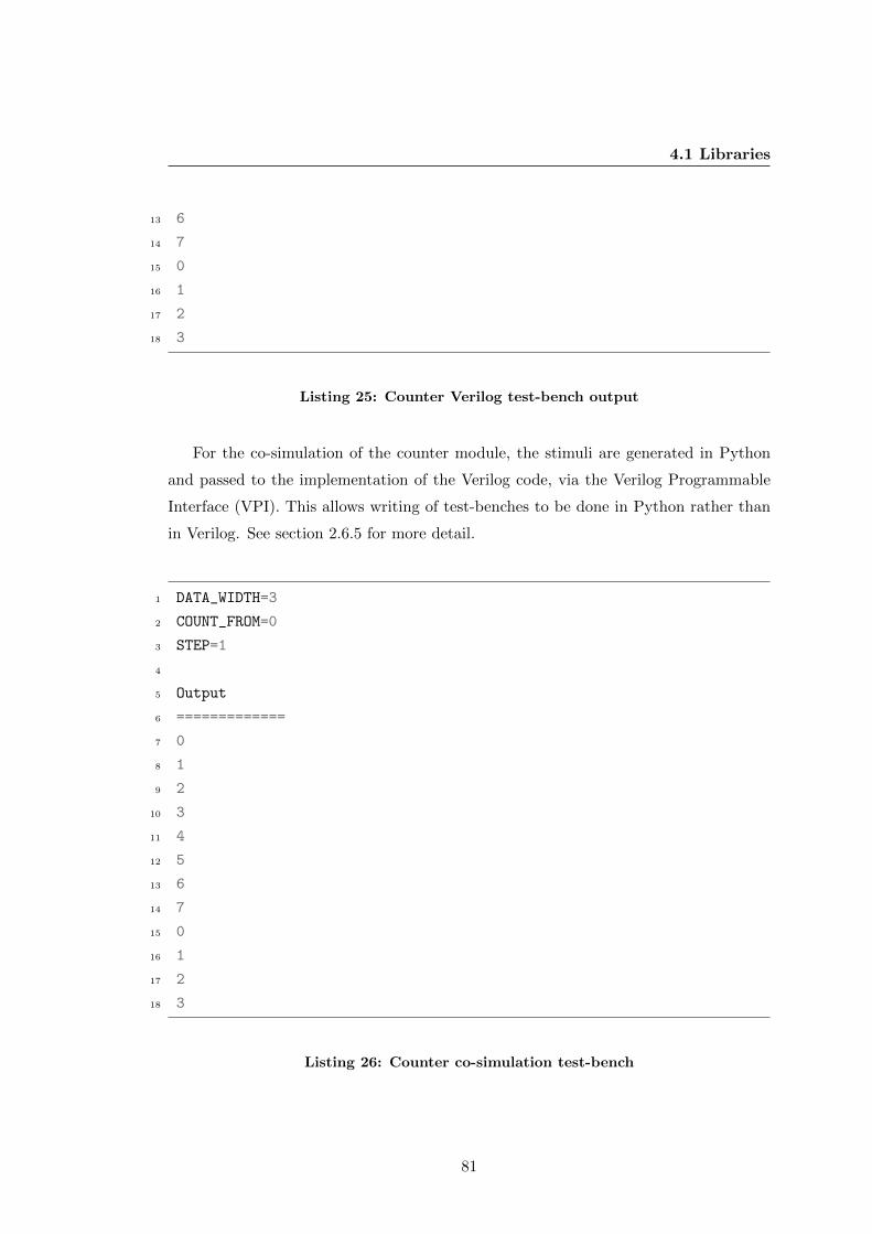
4.1 Libraries
13 6
14 7
15 0
16 1
17 2
18 3
Listing 25: Counter Verilog test-bench output
For the co-simulation of the counter module, the stimuli are generated in Python
and passed to the implementation of the Verilog code, via the Verilog Programmable
Interface (VPI). This allows writing of test-benches to be done in Python rather than
in Verilog. See section 2.6.5 for more detail.
1 DATA_WIDTH=3
2 COUNT_FROM=0
3 STEP=1
4
5 Output
6 =============
7 0
8 1
9 2
10 3
11 4
12 5
13 6
14 7
15 0
16 1
17 2
18 3
Listing 26: Counter co-simulation test-bench
81
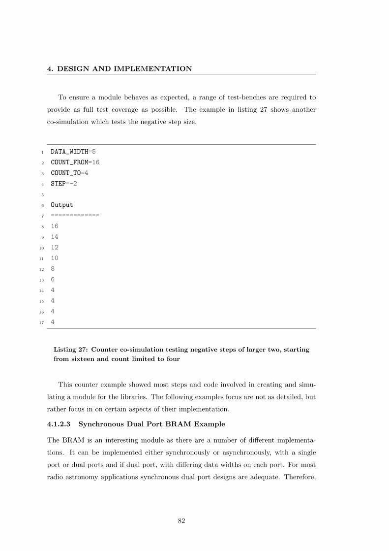
4. DESIGN AND IMPLEMENTATION
To ensure a module behaves as expected, a range of test-benches are required to
provide as full test coverage as possible. The example in listing 27 shows another
co-simulation which tests the negative step size.
1 DATA_WIDTH=5
2 COUNT_FROM=16
3 COUNT_TO=4
4 STEP=-2
5
6 Output
7 =============
8 16
9 14
10 12
11 10
12 8
13 6
14 4
15 4
16 4
17 4
Listing 27: Counter co-simulation testing negative steps of larger two, starting
from sixteen and count limited to four
This counter example showed most steps and code involved in creating and simu-
lating a module for the libraries. The following examples focus are not as detailed, but
rather focus in on certain aspects of their implementation.
4.1.2.3 Synchronous Dual Port BRAM Example
The BRAM is an interesting module as there are a number of different implementa-
tions. It can be implemented either synchronously or asynchronously, with a single
port or dual ports and if dual port, with differing data widths on each port. For most
radio astronomy applications synchronous dual port designs are adequate. Therefore,
82
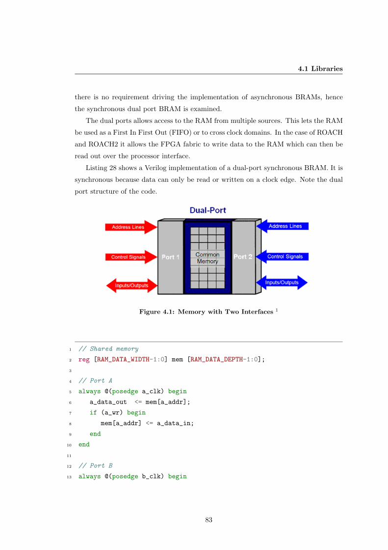
4.1 Libraries
there is no requirement driving the implementation of asynchronous BRAMs, hence
the synchronous dual port BRAM is examined.
The dual ports allows access to the RAM from multiple sources. This lets the RAM
be used as a First In First Out (FIFO) or to cross clock domains. In the case of ROACH
and ROACH2 it allows the FPGA fabric to write data to the RAM which can then be
read out over the processor interface.
Listing 28 shows a Verilog implementation of a dual-port synchronous BRAM. It is
synchronous because data can only be read or written on a clock edge. Note the dual
port structure of the code.
Figure 4.1: Memory with Two Interfaces 1
1 // Shared memory
2 reg [RAM_DATA_WIDTH-1:0] mem [RAM_DATA_DEPTH-1:0];
3
4 // Port A
5 always @(posedge a_clk) begin
6 a_data_out <= mem[a_addr];
7 if (a_wr) begin
8 mem[a_addr] <= a_data_in;
9 end
10 end
11
12 // Port B
13 always @(posedge b_clk) begin
83

4. DESIGN AND IMPLEMENTATION
14 b_data_out <= mem[b_addr];
15 if (b_wr) begin
16 mem[b_addr] <= b_data_in;
17 end
18 end
Listing 28: Verilog Dual Port BRAM
While the tools try to abstract the designer away from the underlying technology,
the BRAM is a good example to show why the designer needs to understand the
architecture of the FPGA. The Xilinx Virtex 6 Series of FPGAs use BRAMs that are
36 bits wide by 1024 bits deep which make them 36k BRAMS. [17] It is important
when deciding what size BRAMs to use in a design, as this could lead to an inefficient
use of the RAM blocks. For example, creating a 37 bit wide BRAM block appends two
RAMs together and wastes 35 bits of the second RAM block.
Dual-port BRAMs also lend themselves to being used as FIFOs. FIFOs are often
used in FPGA designs when moving data between clock domains or for buffering data.
4.1.3 Controller Libraries
The controller modules are generally interfaces to an external peripheral. For example,
the DRAM (Distributed Random Access Memory) controller and are written in Verilog
or generated IP (Intellectual Property) and manage the interfacing to the physical
DRAM hardware. They are wrapped in Python, allowing them to be used in a design
by calling a Python function. These modules are more specific to a particular hardware
platform and FPGA device type, as one hardware platform invariably has different
peripherals to another. For instance, the ROACH board uses Double Data Rate 2
(DDR2) Memory and ROACH2 uses DDR3 Memory which require different controllers.
1
The controller libraries also include modules which are connected to the bus, this
allows devices to interface to the outside world via the processor over the Ethernet
interface. See section 4.3.1 for the detailed memory-mapped bus architecture.
1Refer to www.github.com/wnew/hdl controllers/ for these libraries
84
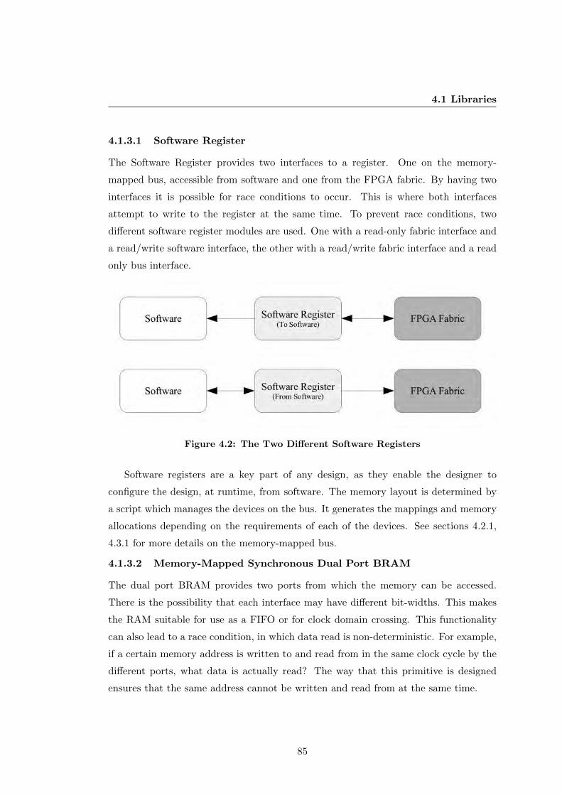
4.1 Libraries
4.1.3.1 Software Register
The Software Register provides two interfaces to a register. One on the memory-
mapped bus, accessible from software and one from the FPGA fabric. By having two
interfaces it is possible for race conditions to occur. This is where both interfaces
attempt to write to the register at the same time. To prevent race conditions, two
different software register modules are used. One with a read-only fabric interface and
a read/write software interface, the other with a read/write fabric interface and a read
only bus interface.
Figure 4.2: The Two Different Software Registers
Software registers are a key part of any design, as they enable the designer to
configure the design, at runtime, from software. The memory layout is determined by
a script which manages the devices on the bus. It generates the mappings and memory
allocations depending on the requirements of each of the devices. See sections 4.2.1,
4.3.1 for more details on the memory-mapped bus.
4.1.3.2 Memory-Mapped Synchronous Dual Port BRAM
The dual port BRAM provides two ports from which the memory can be accessed.
There is the possibility that each interface may have different bit-widths. This makes
the RAM suitable for use as a FIFO or for clock domain crossing. This functionality
can also lead to a race condition, in which data read is non-deterministic. For example,
if a certain memory address is written to and read from in the same clock cycle by the
different ports, what data is actually read? The way that this primitive is designed
ensures that the same address cannot be written and read from at the same time.
85

4. DESIGN AND IMPLEMENTATION
The dual-port memory-mapped BRAM has one interface which is accessible from
the CPU memory-mapped bus and the other from the FGPA fabric. This is imple-
mented by wrapping the dual port BRAM with a module that provides the memory-
mapped interface on to one port. It allows the data stored in the BRAM to be monitored
or modified via the CPU. As the CPU interface is slower than the fabric, it cannot be
piped to the CPU in real-time. The fabric first needs to stop writing to the memory
before it is read by the CPU, otherwise the data may be over-written before it can all
be read out.
Figure 4.3: Memory-Mapped BRAM Wrapper
Figure 4.3 illustrates how the Wishbone interface is attached to port A of the
BRAM, while the other port is left for the fabric. This module is then wrapped in
Python, as with other library modules.
4.1.3.3 Ten Gigabit Ethernet
As with a number of other peripheral controller interfaces, the Ten Gigabit Ethernet
(TGE) core is wrapped in Python in a similar way to the example shown in section
2.6.7 and incorporated into a project in this manner.
constructors On the ROACH2 platform, the TGE can be either SFP+1 or 10GBASE-
CX42 implementations, each of which requires a different controller. The framework
1A low-power 10G Ethernet standard.2The first 10G copper standard published by 802.3
86

4.1 Libraries
decides which one is used by looking at the parameters set by the users. This is also
the case for which of the TGE ports on the ROACH2 the designer wishes to use.
The TGE code is not a single core, but is made up of a couple of modules. Ethernet
consists of layers, as described in the Open Systems Interconnection (OSI) model. The
controller module is normally a combination of the Physical (PHY) and Media Access
Control (MAC) layers, each designed as separate modules in Verilog. This requires the
framework to instantiate both these modules and connect them together, as well as to
the rest of the design.
The TGE also has a CPU interface over which control packets can be sent to the
CPU, processed and, if necessary, replied to. This is a third module for the framework
to include in the TGE module. The designer can select whether or not this interface
is included in the module instantiation by setting the correct parameter in the TGE
configuration.
While it is one of the more complex modules, the TGE is a good example of what
the framework manages and what the controller libraries can provide to the designer.
4.1.4 DSP Libraries
The DSP libraries are the core and purpose of any design. They are where application
designers spend most of their time implementing and developing algorithms. These
libraries also need to provide a good level of flexibility. The DSP Libraries include
modules such as FFTs (Fast Fourier Transforms), Polyphase Filter Banks (PFB) and
Digital Down Converters (DDC). They are constructed by connecting the lower-level
primitive modules in different ways, depending on the specified parameters. This means
that a script needs to be run to configure and connect the underlying modules. With
Python this is easily achievable.
4.1.4.1 FIR Filter
A FIR filter is a good example of a DSP library block that requires flexibility, but can
be easily understood. It is examined in more detail in section 5.3
The FIR Filter module uses a combination of primitive modules. It connects them
together using Python. The basic structure of the FIR filter can be seen in figure 4.4.
The focus in this project is not on the inner workings of the FIR, but on how underlying
modules are dynamically connected to create the upper module.
87

4. DESIGN AND IMPLEMENTATION
Figure 4.4: The Structure of a FIR filter [20]
The code back in listing 21, shows how a library block can be modified using a
block’s parameters. This example is of a filter block with a configurable number of
taps, tap values, tap width, and data width. The tap values are passed as a vector to
the module, which uses them in the instantiation. The module uses a combination of
adders, multipliers and delays to create the filter. Lines 21-25 build the first tap of the
filter and lines 30-37 create the remainder according to the parameters configured.
This filter forms the basis of the final example design, which uses it to filter out
a portion of the band and recover a sinusoidal waveform. See section 5.3 for the FIR
filter example design
To simulate the FIR filter and to test that it is behaving as expected, a filter is
designed using tools available in Python. The taps generated are passed to the filter
as a vector. The simulation input is the sum of two generated sinusoids. One sinusoid
within the pass-band and the other outside the pass-band.
Any hardware provides a limited number of bits, this forces the designer to make
the trade-off between bit-width and precision. The bit-width of this filter was chosen
to be 36 bits, due to the Xilinx 6 series providing multipliers which are 36 bits wide.
[20]
Any filter will cause bit growth, and this makes the choice of tap values that much
more important. A basic FIR filter consists of adders and multipliers, both of which
increase the bit-width of the data being operated on. An adder will cause a bit growth
of one more than the larger of the two values being added. The output bit-width of
88

4.1 Libraries
a multiplier is the sum of the two input bit-widths. The way that this bit-growth is
handled, is to drop the least significant bits of the data after each stage of the filter.
This can easily be handled on an FPGA as the least significant bits automatically get
dropped. This is not a significant problem with a FIR filter, as the output of the filter
is not used to calculate subsequent output values of the filter. This is the case though,
with an Infinite Impulse Response (IIR) filter, hence extra caution is required when
calculating tap values and deciding on bit-widths.
To test the filter library, a set of taps is generated using an web-based tool, T-
Filter1, this can also be done in Matlab or Python. The constraints of the filter are:
a sample rate of 100MHz, a pass band of between 0 and 3MHz and a stop band of
between 10MHz and 50MHz, with a suppression of 40dB. The FIR filter response can
be seen in figure 4.5, with the generated co-efficients on the right.
Figure 4.5: Example FIR Filter Response - Generated with TFilter
The co-efficients can be displayed as double precision numbers or integers. For this
example 36 bit integers are used. The generated filter has 25 taps. The taps are passed
to the filter as a Python list. See listing 21.
1http://t-filter.engineerjs.com
89
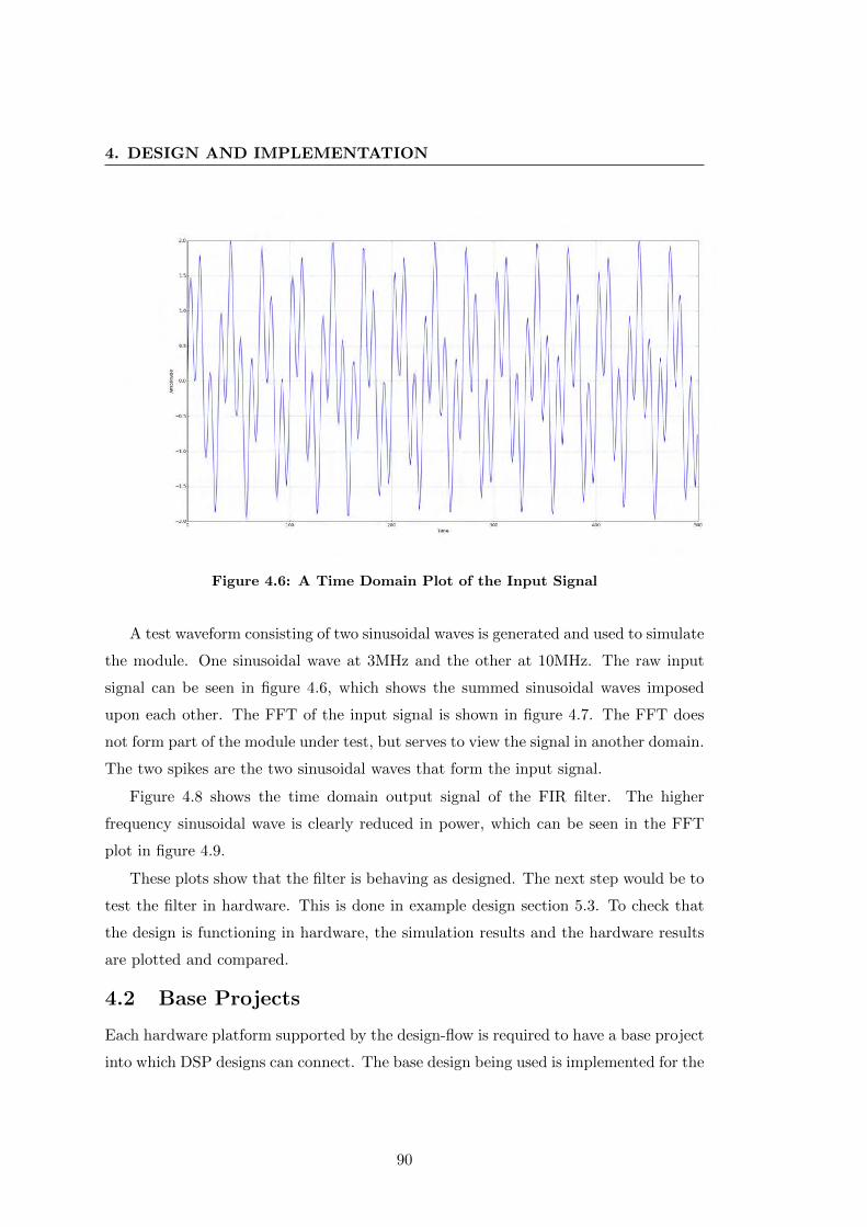
4. DESIGN AND IMPLEMENTATION
Figure 4.6: A Time Domain Plot of the Input Signal
A test waveform consisting of two sinusoidal waves is generated and used to simulate
the module. One sinusoidal wave at 3MHz and the other at 10MHz. The raw input
signal can be seen in figure 4.6, which shows the summed sinusoidal waves imposed
upon each other. The FFT of the input signal is shown in figure 4.7. The FFT does
not form part of the module under test, but serves to view the signal in another domain.
The two spikes are the two sinusoidal waves that form the input signal.
Figure 4.8 shows the time domain output signal of the FIR filter. The higher
frequency sinusoidal wave is clearly reduced in power, which can be seen in the FFT
plot in figure 4.9.
These plots show that the filter is behaving as designed. The next step would be to
test the filter in hardware. This is done in example design section 5.3. To check that
the design is functioning in hardware, the simulation results and the hardware results
are plotted and compared.
4.2 Base Projects
Each hardware platform supported by the design-flow is required to have a base project
into which DSP designs can connect. The base design being used is implemented for the
90
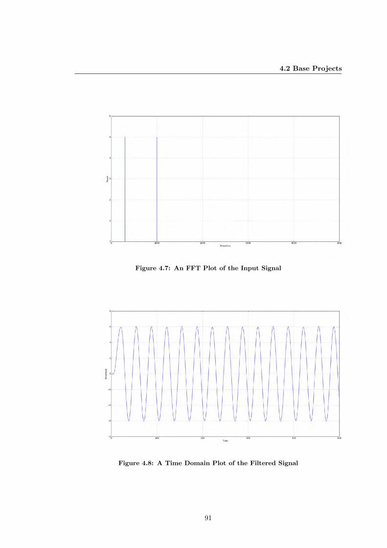
4.2 Base Projects
Figure 4.7: An FFT Plot of the Input Signal
Figure 4.8: A Time Domain Plot of the Filtered Signal
91

4. DESIGN AND IMPLEMENTATION
Figure 4.9: An FFT Plot of the Filtered Signal
ROACH2 hardware platform. The base design consists of: the controllers required to
access the peripherals connected to the FPGA, the bus and the clocking infrastructures,
and the FPGA pin constraints.
The tool-flow is designed around a base project-style architecture. Where each
hardware platform has an associated base project containing the relevant pin constraints
and hardware specific information. The base project is integrated with the modules
used in the design files and used to generate the bitstream files for upload to the
hardware.
The block diagram in figure 4.10 provides an overview of the structure of a typical
base project. It includes the clocking and reset infrastructure. The memory-mapped
bus infrastructure is also shown, it is routed to each device that is connected to the
bus. A basic system block is included, which does basic tasks, such as providing clock
counters and firmware version numbers on the memory-mapped bus. The dashed block
is added once the design is complete and synthesised into a netlist. It is connected to
the interfaces provided by the base project and incorporated into the project. This is
primarily the job of the framework scripts.
92
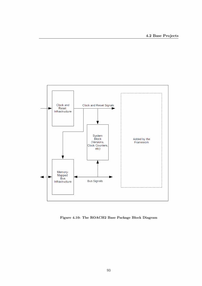
4.2 Base Projects
Figure 4.10: The ROACH2 Base Package Block Diagram
93

4. DESIGN AND IMPLEMENTATION
4.2.1 Memory-Mapped Bus Architecture
The memory-mapped bus architecture is key to the design, as a bad implementation can
cause severe timing issues. The ROACH2 FPGA base package uses the Wishbone bus
and implements: an External Peripheral Bus (EPB) to Wishbone bridge, a Wishbone
arbiter and a range of system registers to store firmware revisions and clock counters.
The memory-mapped bus is accessed via the CPU on the ROACH2 board which is
connected to the FPGA via an EPB bus, hence the need for the EPB to Wishbone
bridge.
The arbiter fans out the bus signals and manages the address to which a transac-
tion is requested. It connects to each device with a separate set of bus wires. This
architecture worked for the test system where the number of devices on the bus was
minimal. However, is not ideal for larger designs, due to the fanout caused by this bus
implementation technique which leads to routing and timing issues. Other methods of
bus implementation are discussed in the framework in section 4.3.1.
4.2.2 Reset Infrastructure
A system-wide reset infrastructure is implemented in the base package. This is not
always essential as many designs do not require a system-level reset, but reset only the
DSP or sections of the design independently where required. So the tool-flow allows
the designer to reset specific blocks as needed.
4.2.3 Clocking Infrastructure
The functionality of the clocking infrastructure is split between the base project and
the framework. The framework manages the connecting of the clocks to the necessary
blocks and the base project provides the infrastructure for creating the clocks at the
correct frequencies.
Ideally, the application designer should not have to manage the clock infrastructure,
further than specifying the clock domain/s that are to be used in the design. This
is managed by a combination of the Framework scripts and the base project. The
base project clock infrastructure for the ROACH2 uses Mixed-Mode Clock Managers
(MMCM) [16] to generate the required clocks. The main fabric clock can be selected
from a number of different sources. On the ROACH2 board, this is either the crystal
clock on the Printed Circuit Board (PCB), an external clock via the ADC mezzanine
cards or an external clock from a SubMiniature version A (SMA) connector. The
94
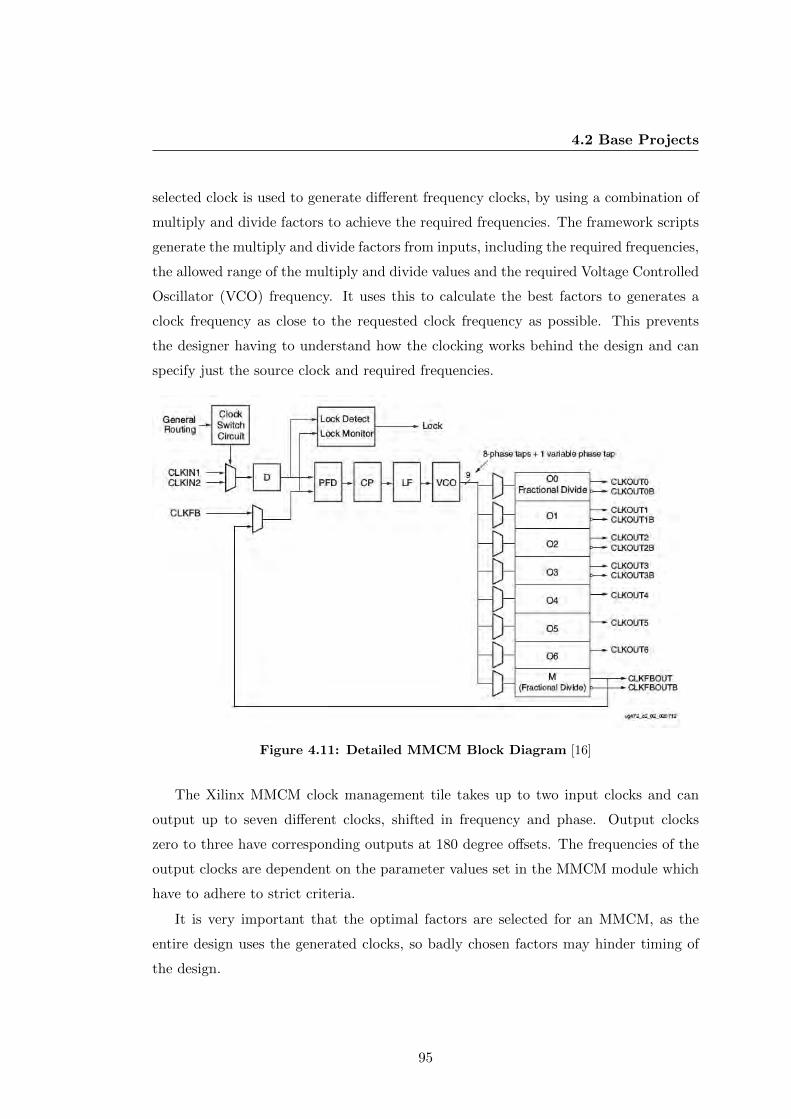
4.2 Base Projects
selected clock is used to generate different frequency clocks, by using a combination of
multiply and divide factors to achieve the required frequencies. The framework scripts
generate the multiply and divide factors from inputs, including the required frequencies,
the allowed range of the multiply and divide values and the required Voltage Controlled
Oscillator (VCO) frequency. It uses this to calculate the best factors to generates a
clock frequency as close to the requested clock frequency as possible. This prevents
the designer having to understand how the clocking works behind the design and can
specify just the source clock and required frequencies.
Figure 4.11: Detailed MMCM Block Diagram [16]
The Xilinx MMCM clock management tile takes up to two input clocks and can
output up to seven different clocks, shifted in frequency and phase. Output clocks
zero to three have corresponding outputs at 180 degree offsets. The frequencies of the
output clocks are dependent on the parameter values set in the MMCM module which
have to adhere to strict criteria.
It is very important that the optimal factors are selected for an MMCM, as the
entire design uses the generated clocks, so badly chosen factors may hinder timing of
the design.
95

4. DESIGN AND IMPLEMENTATION
As an example, assuming a designer wanted to generate two clocks one of 250MHz
and one of 125MHz from the ROACH2’s on-board 100MHz clock. Firstly, the MMCM
will multiply up the clock frequency into the range of the VCO, in the case of the Virtex
6 this is between 600MHz and 1200MHz. Then it is divided back down to the required
values. The range of the multiply and divide values is also limited. The multiply factor
can be an integer between five and sixty four and the divide factor can be an integer
between one and eighty. The Python script assesses the frequencies of the output clocks
and selects the best multiply and divide factors to achieve this.
These clocks are then exposed to the designer, in that each library module in the de-
sign needs to have a clock assigned to it. The designer can select from the preconfigured
list of application clocks for each module.
4.2.4 Controllers
Each base project provides an associated library of gateware controller blocks which
facilitate control of the peripherals that are accessible from the FPGA fabric. These
include, but are not limited to: Dynamic Read Only Memory (DRAM), Quad Data
Rate (QDR), Analog to Digital Converters (ADC), Digital to Analog Converters (DAC)
and Ethernet. The controllers provide a number of parameters that are configurable by
the application designer and are required to be thoroughly tested before being added
to the libraries.
The base project in conjunction with the framework, knows which controllers are
supported on each hardware platform. It performs a pre-compilation dynamic rules
check on designs to ensure only supported controllers are used. The rules also ensure
only supported clocks are selected and the memory-mapped bus is configured correctly.
For a detailed description of selected controllers, see section 4.1.3.
4.2.5 Constraints
FPGA constraints provide additional information to the tools, over and above the
HDL design. These include: pin locations, timing constraints and design constraints
(placement of parts of the design in a particular area of the FPGA fabric).
A constraints file for each hardware platform is provided with the corresponding
base project. It includes all the constraints that are required for that hardware platform.
The framework adds to this file pre-compilation, depending on the controllers and
library blocks used in the design. For instance, if an ADC is added to the design,
96

4.3 Framework
the correct pins locations are added to the pin constraints file. Here the base package
provides the default constraints files and the framework appends to it where necessary.
4.3 Framework
The tool-flow architecture is written in Python. It manages the entire process from
the design to the silicon. It takes the design files and perform a preliminary design
rules check. It then generates the required HDL files from the MyHDL, as well as the
top-level HDL file, which pulls the modules together. The compilation parameters are
generated and then the compilation run. The framework manages all aspects of the
flow of a design, from redrawing of blocks to the compile process.
4.3.1 Bus Infrastructure
Where the libraries provide the devices, the base project provides the bus master and
arbiter, the framework is responsible for connecting up devices to the bus arbiter and
giving each a unique memory address range. See section 4.2.1.
The Python framework manages the bus infrastructure by iterating through all
the blocks in a design. If a block requires a bus interface, it sets the bus controllers
parameters and then connects the device to the bus arbiter. This means that the bus
architecture will need to have the flexibility to handle almost any amount of devices,
within reason. The way that this is implemented is to have a controller capable of
handling X amount of devices and if the devices exceed X then a space on the initial
arbiter is used to add another arbiter level. The drawback is, that each cascaded
controller adds extra latency to the devices further down the chain.
The bus architecture could be implemented in one of four different ways, each with
different trade-offs. Firstly, the devices could be daisy chained. This provides the best
case for routing but the worst case for latency. See figure 4.13. The second method
is by sharing the data lines. See figure 4.14. Although, this requires that each device
on the bus needs to release the data lines when it is not being addressed. In other
words, it requires a tristate buffer, but the newer Xilinx devices do not support tristate
buffers internal to the FPGA fabric and instead use a multiplexer with a floating input.1
Thirdly, the controller could have dedicated bus lines for each device, this produces a
1Tristate buffers are implemented as a multiplexer with one port floating. This allows a device on
the bus to not drive the bus lines when not addressed, letting other devices use the bus. See figure
4.12, Table 4.1
97

4. DESIGN AND IMPLEMENTATION
large fanout with many wires to route around the FPGA, as well as a large multiplexer
at the controller. If the data address is 32 bits wide the multiplexer would be have 32
* the amount of devices inputs. See figure 4.15. The forth option is a hybrid of the
second and third. The number of devices that an arbiter can support is limited and
once that limit is reached another arbiter is attached to the first so that more devices
can be attached to the bus. This creates a tree structure which reduces the fanout and
the size of the multiplexer and only slightly increase the latency. See figure 4.16.
Figure 4.12: Tristate Buffer Implementation
A B S O
0 Z 0 0
1 Z 0 1
0 Z 1 Z
1 Z 1 Z
Table 4.1: Truth Table for a two input multiplexer with input B floating
Figure 4.13: Daisy Chained Bus Configuration - Easy routing, higher latency
The design of the devices that connect to the bus is tightly coupled to the design of
the arbiter. If the arbiter shares the data lines between the devices, each device needs
98

4.3 Framework
Figure 4.14: Single Bus Configuration - All devices share the same bus
Figure 4.15: Fanned Out Bus Configuration - Dedicated bus per device
Figure 4.16: Tree Bus Configuration - Less large multiplexers
99

4. DESIGN AND IMPLEMENTATION
to ensure that its only drive the data lines when they are being addressed, otherwise
the entire bus is unusable or the design will not compile due to multiple drivers on a
wire.
4.3.2 Clocking Infrastructure
The clocking functionality is shared between the base project and the framework. The
base project provides the instantiations of the clock management modules. The frame-
work calculates the parameters to pass to the clock management modules to generate
the clocks at the required frequencies for the application design. See section 4.2.3 for
the base project’s role in the clock management.
The framework is also responsible for managing the clock domains and ensuring the
correct clock gets to each module in the design.
4.3.3 Redrawing of Library Modules
An important feature of the framework is the redrawing of the DSP library modules,
which is dependent on the parameters provided in the design. This connects underlying
blocks in different ways depending on the values of the parameters.
This functionality is handled in each Python wrapper in the DSP libraries. A good
example of this is a basic FIR filter. If the parameter for the number of taps is changed,
then the way that the underling adders, multipliers and delays are connected is changed.
See sections 4.1.4.1 and 4.1.1.4
The best way to show how blocks are redrawn is to examine a Simulink example.
Although, it is a Simulink model the Python works exactly the same way, just without
a graphical interface. Figure 4.18 shows the internals of the PFB FIR block configured
with two taps when this is changes to four taps the redrawn internals can be seen in
figure 4.19. Figure 4.17 shows the configuration parameters and the PBF FIR block.
This is a very useful feature of the tools, as it provides flexibility to create fewer
library blocks which cover a large range of functionality. It could also be implemented
at the level of a filter block, which has a drop down list of different types of filters.
Each filter would have an associated list of parameters. Ultimately, this functionality
is core to the tool-flow and provides designers with a good level of flexibility.
4.3.4 Incorporation of the DSP Application into the Base Package
It is the responsibility of the framework to incorporate the DSP design netlist into the
base package. This involves taking the base package top-level design file, instantiating
100

4.3 Framework
Figure 4.17: PFB FIR and configuration parameters
Figure 4.18: Internals of the PFB FIR 1 Number of taps set to two
101
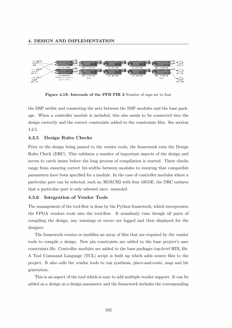
4. DESIGN AND IMPLEMENTATION
Figure 4.19: Internals of the PFB FIR 2 Number of taps set to four
the DSP netlist and connecting the nets between the DSP modules and the base pack-
age. When a controller module is included, this also needs to be connected into the
design correctly and the correct constraints added to the constraints files. See section
4.2.5.
4.3.5 Design Rules Checks
Prior to the design being passed to the vendor tools, the framework runs the Design
Rules Check (DRC). This validates a number of important aspects of the design and
serves to catch issues before the long process of compilation is started. These checks
range from ensuring correct bit-widths between modules to ensuring that compatible
parameters have been specified for a module. In the case of controller modules where a
particular port can be selected, such as, ROACH2 with four 10GbE, the DRC endures
that a particular port is only selected once. amended
4.3.6 Integration of Vendor Tools
The management of the tool-flow is done by the Python framework, which incorporates
the FPGA vendors tools into the tool-flow. It seamlessly runs though all parts of
compiling the design, any warnings or errors are logged and then displayed for the
designer.
The framework creates or modifies an array of files that are required by the vendor
tools to compile a design. New pin constraints are added to the base project’s user
constraints file. Controller modules are added to the base packages top-level HDL file.
A Tool Command Language (TCL) script is built up which adds source files to the
project. It also calls the vendor tools to run synthesis, place-and-route, map and bit
generation.
This is an aspect of the tool which is easy to add multiple vendor support. It can be
added as a design as a design parameter and the framework includes the corresponding
102
4.4 Testing
vendor files and builds to TCL files accordingly.
As the board that the tool-flow is tested on is the ROACH2 hardware platform with
a Xilinx Virtex 6 FPGA, the Xilinx tools are be the first to be incorporated into the
framework. Xilinx has provided command-line access to all of its tools via TCL, which
can be scripted to call each tool with parameters set up in the design configuration.
4.3.7 Simulation
The simulation of a design is managed by the framework via the MyHDL Python
package. The framework calls MyHDL which is responsible for running the simulation
and outputs it to a Value Change Dump (VCD) file which can be opened and viewed
using a waveform viewer. See section 2.6.4 for a more detailed description of the
simulation functionality of MyHDL.
4.4 Testing
Once the design-flow is implemented, it is imperative to test it. This is done by creating
a couple of designs, ranging from simple to more complex designs. Each example design
targets a specific aspect of the tool-flow to test that particular functionality. The details
of these example designs are examined in the following chapter.
103

4. DESIGN AND IMPLEMENTATION
104

Chapter 5
Example Designs
In order to examine how the tool-flow performs when used for designing applications,
it is necessary to design applications that exercise as many aspects of the tools-flow as
possible. The initial test design is a basic counter which is used to test the base project
functionality. A more complex filter application is used to test a range of modules from
the adders and multipliers to the filter itself.
5.1 Binary Counting LEDs
The binary counting Light Emitting Diodes (LED) design consists of a counter which
is connected to the LEDs on the ROACH2 board. It is a 32 bit counter which toggles
the eight LEDs using the top bits of the counter register. The design runs off a 100MHz
clock, meaning that the 32 bit counter wraps about every 42 seconds, toggling the eight
most significant LEDs slowly enough to be visually observed.
The aim of the simple counter design is to test that the basic features of the design-
flow are working correctly. It requires the framework of the design-flow to insert the
counter module into the existing ROACH2 base package, to generate the counter wrap-
per module and to pass the design files to the Xilinx Integrated Synthesis Environment
(ISE) tool for synthesis, map, place-and-route and bit generation.
5.1.1 Design of the Binary Counting LEDs
To allow toggling of the LEDs at rate that is visible to the human eye, the top 8 bits
of a 32 bit counter are used. A 32 bit register can store a value of up to 4,924,967,295,
which if divided by the clock frequency of 100MHz gives 42.9 seconds. This is the time
105

5. EXAMPLE DESIGNS
that the counter takes to wrap. Therefore, using the top 8 bits ensures that the LEDs
count slowly enough to be visible.
To pass only the 8 most significant bits to the LED pins, a slice block is used. It
is configured such that the input is 32 bits and the output is the eight most significant
bits of the input.
The output of the slice block is passed to the LED block which assigns the LED
pins on the FPGA to the output signals of the slice block. The block diagram design
of this design can be seen in figure 5.1
Figure 5.1: The Counting LEDs Design Block Diagram - The supporting infras-
tructure is in light gray
The block diagram also shows, in a lighter gray colour, the supporting infrastructure.
Which, in this case, is just the clocking and reset infrastructure. Only the counter needs
the clock and reset, as the slice block is asynchronous to the clock, meaning that its
outputs are only a function of its inputs and are not triggered on a clock edge.
There are two ways to simulate this design, these are covered in the following
sections.
5.1.2 Python Simulation
This particular design requires only simple input to simulate. The input signals are
the clock and the reset. Once these signals are driven, the counter runs freely and
continues to do so until the end of the simulation. The other example designs require
more complex simulation sources. See sections 4.1.4.1 and 5.2.2
106

5.1 Binary Counting LEDs
The Python simulation of the LED counting design outputs the data in figure 29.
See the simulation code in listing 23. This data can easily be plotted or visualised by
any method required. In this case text is ideal for visually ensuring that the counter is
incrementing by one each cycle. It could also be displayed in decimal or hexadecimal.
As the LEDs represent binary counting, the simulation output is binary. It clearly
shows that the design behaves as is expected.
1 xxxxxxxx
2 00000000
3 00000001
4 00000010
5 00000011
6 00000100
7 00000101
8 ...
9 00011011
10 00011100
11 00011101
12 00011110
13 00011111
Listing 29: Text output of the sliced counter simulation
5.1.3 HDL Bit Accurate Simulation
Due to the time required to simulate a 32 bit counter, which is over 1000 million
cycles, the design was modified to use only the first 8 bits of the counter for a quicker
simulation.
As can be seen from the wave form simulation in figure 5.2, the output of the
slice block is only 8 bits wide, hence it wraps after 256 cycles. Whereas, the counter
continues counting. This is confirmation that 8 bits are being slicing bits off the counter
and shows that the top most bits are sliced correctly. The clock, enable and reset signals
can be seen in the simulation as well. The reset is high because in this example it is
an active low reset.
107
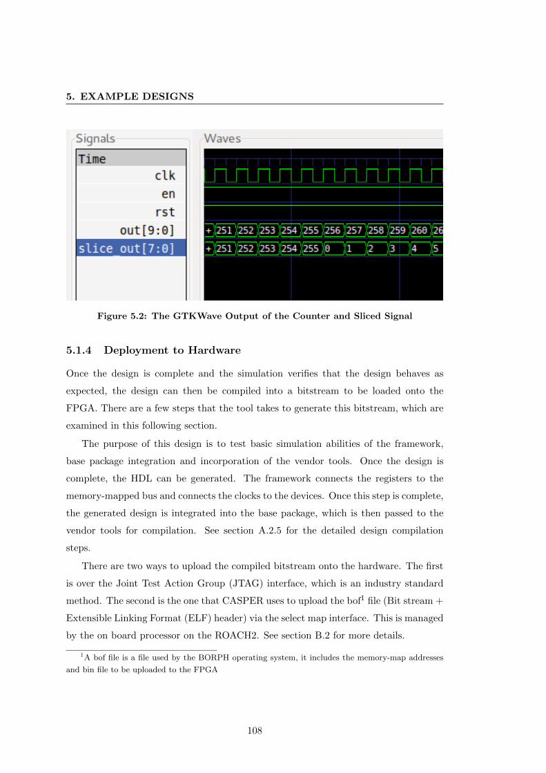
5. EXAMPLE DESIGNS
Figure 5.2: The GTKWave Output of the Counter and Sliced Signal
5.1.4 Deployment to Hardware
Once the design is complete and the simulation verifies that the design behaves as
expected, the design can then be compiled into a bitstream to be loaded onto the
FPGA. There are a few steps that the tool takes to generate this bitstream, which are
examined in this following section.
The purpose of this design is to test basic simulation abilities of the framework,
base package integration and incorporation of the vendor tools. Once the design is
complete, the HDL can be generated. The framework connects the registers to the
memory-mapped bus and connects the clocks to the devices. Once this step is complete,
the generated design is integrated into the base package, which is then passed to the
vendor tools for compilation. See section A.2.5 for the detailed design compilation
steps.
There are two ways to upload the compiled bitstream onto the hardware. The first
is over the Joint Test Action Group (JTAG) interface, which is an industry standard
method. The second is the one that CASPER uses to upload the bof1 file (Bit stream +
Extensible Linking Format (ELF) header) via the select map interface. This is managed
by the on board processor on the ROACH2. See section B.2 for more details.
1A bof file is a file used by the BORPH operating system, it includes the memory-map addresses
and bin file to be uploaded to the FPGA
108
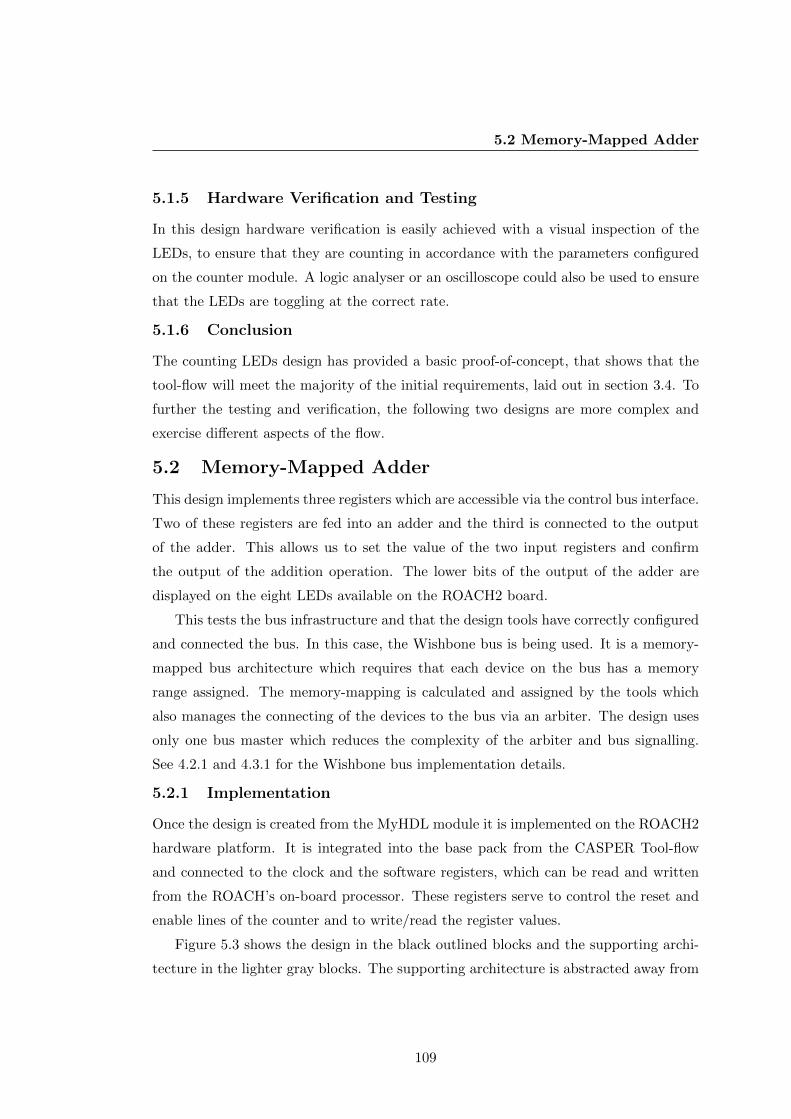
5.2 Memory-Mapped Adder
5.1.5 Hardware Verification and Testing
In this design hardware verification is easily achieved with a visual inspection of the
LEDs, to ensure that they are counting in accordance with the parameters configured
on the counter module. A logic analyser or an oscilloscope could also be used to ensure
that the LEDs are toggling at the correct rate.
5.1.6 Conclusion
The counting LEDs design has provided a basic proof-of-concept, that shows that the
tool-flow will meet the majority of the initial requirements, laid out in section 3.4. To
further the testing and verification, the following two designs are more complex and
exercise different aspects of the flow.
5.2 Memory-Mapped Adder
This design implements three registers which are accessible via the control bus interface.
Two of these registers are fed into an adder and the third is connected to the output
of the adder. This allows us to set the value of the two input registers and confirm
the output of the addition operation. The lower bits of the output of the adder are
displayed on the eight LEDs available on the ROACH2 board.
This tests the bus infrastructure and that the design tools have correctly configured
and connected the bus. In this case, the Wishbone bus is being used. It is a memory-
mapped bus architecture which requires that each device on the bus has a memory
range assigned. The memory-mapping is calculated and assigned by the tools which
also manages the connecting of the devices to the bus via an arbiter. The design uses
only one bus master which reduces the complexity of the arbiter and bus signalling.
See 4.2.1 and 4.3.1 for the Wishbone bus implementation details.
5.2.1 Implementation
Once the design is created from the MyHDL module it is implemented on the ROACH2
hardware platform. It is integrated into the base pack from the CASPER Tool-flow
and connected to the clock and the software registers, which can be read and written
from the ROACH’s on-board processor. These registers serve to control the reset and
enable lines of the counter and to write/read the register values.
Figure 5.3 shows the design in the black outlined blocks and the supporting archi-
tecture in the lighter gray blocks. The supporting architecture is abstracted away from
109
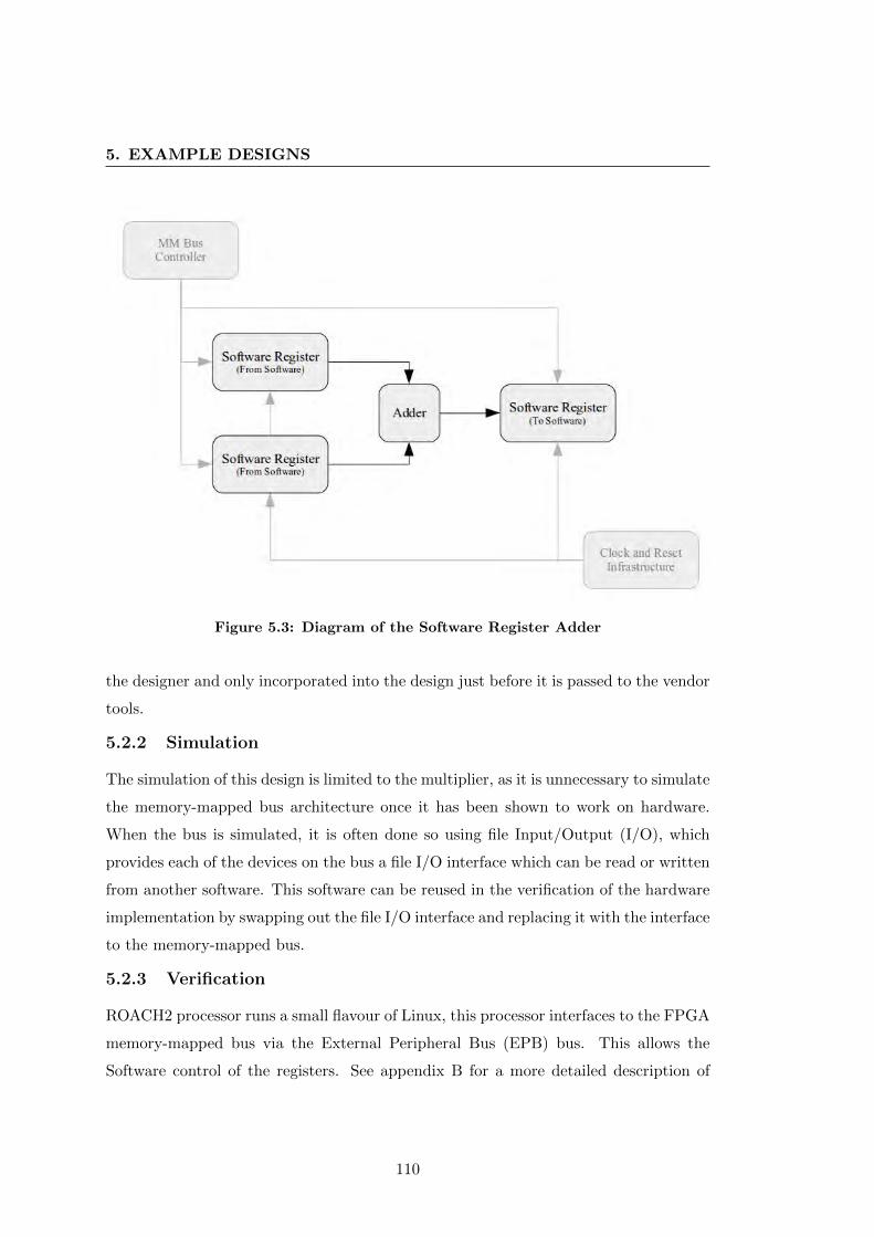
5. EXAMPLE DESIGNS
Figure 5.3: Diagram of the Software Register Adder
the designer and only incorporated into the design just before it is passed to the vendor
tools.
5.2.2 Simulation
The simulation of this design is limited to the multiplier, as it is unnecessary to simulate
the memory-mapped bus architecture once it has been shown to work on hardware.
When the bus is simulated, it is often done so using file Input/Output (I/O), which
provides each of the devices on the bus a file I/O interface which can be read or written
from another software. This software can be reused in the verification of the hardware
implementation by swapping out the file I/O interface and replacing it with the interface
to the memory-mapped bus.
5.2.3 Verification
ROACH2 processor runs a small flavour of Linux, this processor interfaces to the FPGA
memory-mapped bus via the External Peripheral Bus (EPB) bus. This allows the
Software control of the registers. See appendix B for a more detailed description of
110

5.2 Memory-Mapped Adder
how the control and monitoring on the ROACH boards work. This control interface
allows the registers to be read and written remotely over the network.
1 # imports correlator package
2 import corr
3 # imports random integer generator
4 from random import randint
5 # create an object that managed the connection to the ROACH2 board
6 fpga = corr.katcp_wrapper.FpgaClient(<IP>)
7
8 # repeat for however many tests required
9 for i in range(100):
10 # generate random integers between 0 and 10000
11 in1 = randint(0, 10000)
12 in2 = randint(0, 10000)
13 # write the random integers to the FPGA registers in1 and in2
14 fpga.write_int(’input1’, in1)
15 fpga.write_int(’input2’, in2)
16 # read the output register
17 out = fpga.read_int(’output’)
18 # check if the output register contains the expected value
19 if (out != in1+in2):
20 print(’fail’)
21 print(out)
Listing 30: Python script to test the addition of two registers of the ROACH2
board
The Python script above tests the addition design. In this case it writes and reads
the output one hundred times. This can be done without a delay between the write
and read, as the result will propagate to the output register in two clock cycles. This is
many times shorter than the network latency for read or write request. It is important
to remember, that the registers are all 32 bits wide, meaning that, if the value of the
two input registers add up to more then 32 bits the output register will wrap. In order
to prevent this, the input simulation values are kept low.
111

5. EXAMPLE DESIGNS
The script to test this design passes, ensuring that the implementation is correct
and working as expected. This shows that the Wishbone bus is connected correctly,
which is the aspect of the tool-flow that is being tested by this design.
To further verify this, the LEDs are connected to the least significant 8 bits of the
output of the adder so that the output can, at the same time, be partially verified
visually.
5.3 Low-Pass FIR Filter
To show the power of MyHDL to simulate and implement a working Digital Signal
Processing (DSP) design, a low-pass Finite Impulse Response (FIR) filter is designed
simulated and deployed on the ROACH2 hardware platform. The purpose of this
example is to compare the simulation outputs with the outputs of the design when
implemented in hardware. This will give a good indication of the accuracy of the
simulation and demonstrates the tool-flow being used to implement a real-world DSP
application.
5.3.1 Overview
The diagram of this design can be seen in figure 5.4. The input into the system is
an Analog to Digital Converter (ADC), in this case the KATADC. The controller has
been written in Verilog and wrapped in MyHDL. The ADC can be configured via an
Inter-Integrated Circuit (IIC or I2C) interface, but the default configuration is fine for
this design. The ADC receives an input clock of 400MHz, which in the case of the
KATADC is demultiplexed by four before being routed to the FPGA. This clock is
used as the FPGA design clock, running at 100MHz.
The sampled data from the ADC is then fed into the filter. This is the basic FIR
filter described in section 4.1.4.1. The same set of taps used in the simulation is used
in this design, so the the output of the simulation and the implementation can be
compared.
The data outputted from the filter is stored in a Block Random Access Memory
(BRAM). The BRAM in this design is 72 kilobits deep, which allows 72 000 samples to
be stored. The BRAM is implemented as a snap-block, which means that the user can
write a register to trigger the BRAM to start capturing data. The BRAM is then fully
written and the writing stops. The user can then read the data out of the BRAM, via
the CPU interface, for post-processing.
112
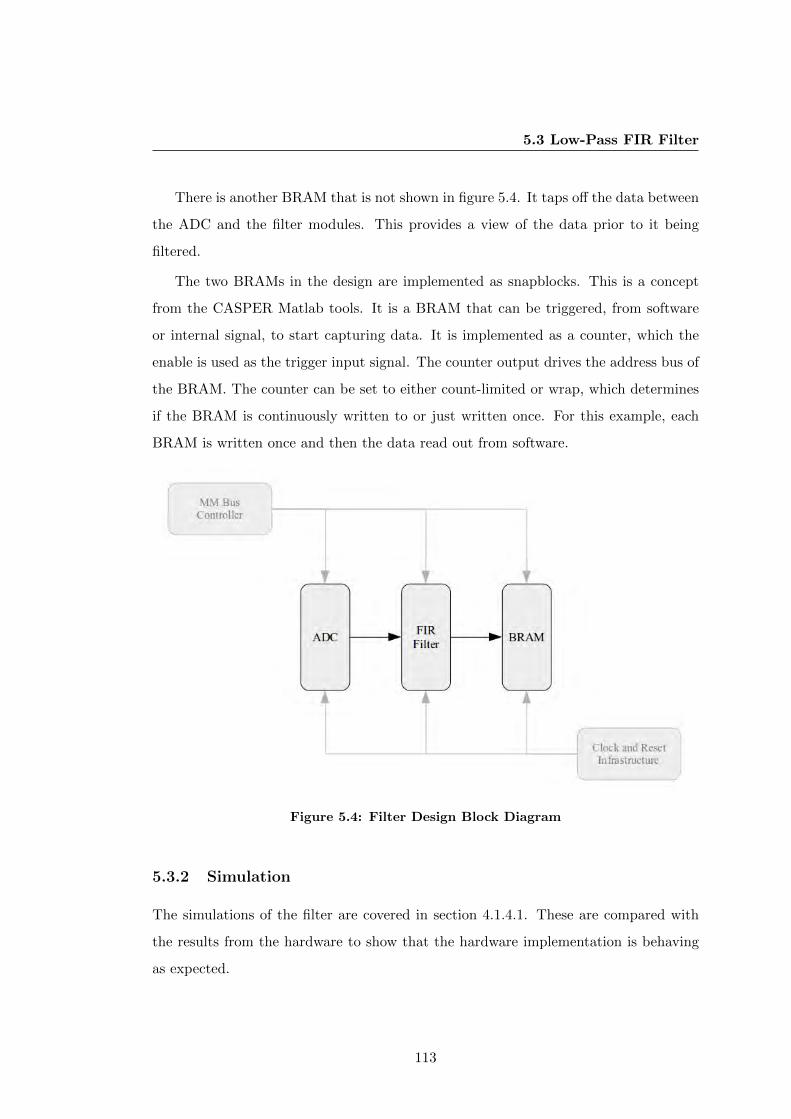
5.3 Low-Pass FIR Filter
There is another BRAM that is not shown in figure 5.4. It taps off the data between
the ADC and the filter modules. This provides a view of the data prior to it being
filtered.
The two BRAMs in the design are implemented as snapblocks. This is a concept
from the CASPER Matlab tools. It is a BRAM that can be triggered, from software
or internal signal, to start capturing data. It is implemented as a counter, which the
enable is used as the trigger input signal. The counter output drives the address bus of
the BRAM. The counter can be set to either count-limited or wrap, which determines
if the BRAM is continuously written to or just written once. For this example, each
BRAM is written once and then the data read out from software.
Figure 5.4: Filter Design Block Diagram
5.3.2 Simulation
The simulations of the filter are covered in section 4.1.4.1. These are compared with
the results from the hardware to show that the hardware implementation is behaving
as expected.
113

5. EXAMPLE DESIGNS
5.3.3 Hardware Setup
The design is deployed on a ROACH2. The ROACH2 has an IADC as the Radio
Frequency (RF) front end, which is clocked at 400MHz.
The input signal is generated using two signal generators: one set to 3MHz and the
other set to 10MHz. The 10MHz having slightly less power. The signals are combined
using a splitter connected in reverse orientation. The output of the splitter is then fed
to the input of the ADC.
The ROACH2 is networked to a server, which can interface to the design, primarily
for control and monitoring. In this example, the filtered waveform is stored in BRAM
on the FPGA and read out over the control interface. Even though it is a slow interface
only a few samples need to be captured.
5.3.4 Results
Once the design is deployed on hardware, the BRAMs can be triggered from software
to start capturing data. At 100MHz the 72 kilobit BRAMs are filled up in less than
one millisecond and are ready to be read from software.
A script is run to trigger the capture and to read out the captured data. The plots
in figures 5.5, 5.7, 5.6 and 5.8 show the captured data.
Figure 5.5: Time Domain Plot of the Sampled Signal - Prefilter
114
5.3 Low-Pass FIR Filter
The summed sinusoidal waves are visible in figure 5.5. This is the signal as sampled
by the ADC. The FFT of this signal can be seen in figure 5.6.
Figure 5.6: FFT Plot of the Sampled Signal - Prefilter
The plot in figure 5.7 is the output of the low-pass filter. It shows how the power
of the higher frequency part of the signal is reduced. The FFT of the output of the
filter shown in figure 5.8, confirms the reduction in power of the 10MHz component of
the signal.
As expected, these results align with the simulations shown in section 4.1.4.1.
115
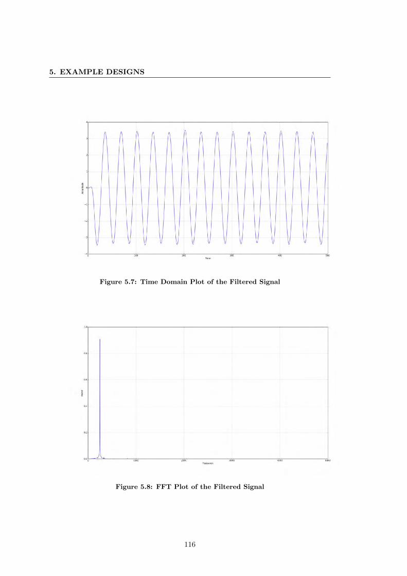
5. EXAMPLE DESIGNS
Figure 5.7: Time Domain Plot of the Filtered Signal
Figure 5.8: FFT Plot of the Filtered Signal
116

Chapter 6
Results and Conclusion
In this dissertation a Python-based Field Programmable Gate Array (FPGA) tool-
flow has been designed, implemented and tested. The hardware that is targeted and
tested on is the Reconfigurable Open Architecture Computing Hardware 2 (ROACH2)
platform, which uses the Xilinx Virtex 6 FPGA. The MyHDL framework is used for the
core of the tool-flow and provides features such as simulation and modelling for the flow.
Three example designs are created, including a simple Finite Impulse Response (FIR)
filter, to test the functionality and limitations of the flow. The example designs show
that the objective of designing a tool-flow around MyHDL is a feasible proposal. The
simulation and integration ability it provides, in conjunction with Python are ideally
suited to this type of development.
6.1 Results
The results from the example designs show that the tool-flow meets the majority of
the objectives set out in section 1.3. Whether or not it is any better than traditional
methods of FPGA design is discussed in the following section. For the detailed results
of the example designs see 5.1.6, 5.2.3 and 5.3.4
The first example design is the binary counting Light Emitting Diodes (LED). The
purpose of this design is to test if a design can be incorporated into the base package
successfully. This proved to be the case. Once the design is deployed, the LEDs on the
ROACH2 board can be seen to count in binary. This is the behaviour expected.
The second design is the software registers on the memory-mapped bus. The pur-
pose of this design is to test if the bus can be generated automatically and can be
117

6. RESULTS AND CONCLUSION
deployed to the FPGA. This was successfully achieved and the registers can be written
and read as desired. This shows that the memory-mapped bus is implemented and
working correctly.
The final example design is that of the FIR filter. Its purpose is to test that the
simulation of a Digital Signal Processing (DSP) design matches the output of the final
deployed design. The results of the simulation can be seen in figure 6.1 and the results
from the hardware system are seen in 6.2. By observing the plots, the similarity can
clearly be seen. This shows that the tool-flow can simulate a design and the results can
be trusted to match the hardware implementation. For the more detailed analysis of
these results see 5.3.4
Figure 6.1: Simulation Time Domain and FFT Plots
6.2 Measures of Success
The results from the example designs proved successful. As per section 3.1, there are
two other methods of measuring the success of the tool-flow implementation. Firstly,
the implementation of the features listed in the requirements. Secondly, the predefined
metrics, such as ease of use and reliability.
118
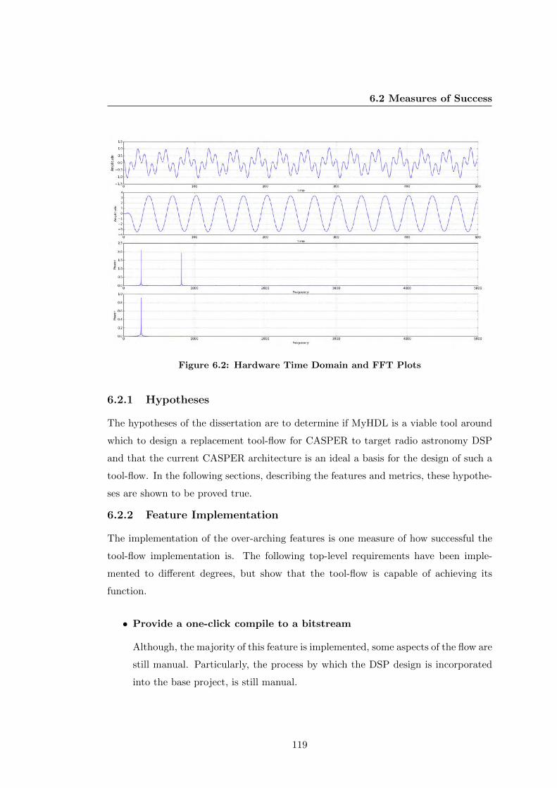
6.2 Measures of Success
Figure 6.2: Hardware Time Domain and FFT Plots
6.2.1 Hypotheses
The hypotheses of the dissertation are to determine if MyHDL is a viable tool around
which to design a replacement tool-flow for CASPER to target radio astronomy DSP
and that the current CASPER architecture is an ideal a basis for the design of such a
tool-flow. In the following sections, describing the features and metrics, these hypothe-
ses are shown to be proved true.
6.2.2 Feature Implementation
The implementation of the over-arching features is one measure of how successful the
tool-flow implementation is. The following top-level requirements have been imple-
mented to different degrees, but show that the tool-flow is capable of achieving its
function.
• Provide a one-click compile to a bitstream
Although, the majority of this feature is implemented, some aspects of the flow are
still manual. Particularly, the process by which the DSP design is incorporated
into the base project, is still manual.
119

6. RESULTS AND CONCLUSION
• Provide the functionality to model, simulate and verify designs using
a high-level language
This feature is implemented by virtue of using MyHDL as the framework. It
allows Python to be used as the modelling language and brings all the maths and
plotting features of Python and its packages.
6.2.2.1 Libraries
The libraries for a key part of the tool-flow. A well designed set of libraries with good
coverage provides the designer with the tools needed to implement a design. Thus, it
is important that this requirement is met.
• Primitive Library
A range of primitive libraries has been implemented and included in the library.
Although, there are still others that could be added. Due to the scope and time
limitations, these are not implemented.
• Controller Library
The controllers used for the example designs have been added to the libraries.
These are the Ten Gigabit Ethernet and the IADC. Generally these are board
specific, so as more boards are supported, more controller libraries would need to
be written.
• DSP Library
The FIR Filter used in the filter example design is incorporated into the libraries.
Other DSP blocks would need to be developed in the future.
6.2.2.2 Framework
The framework pulls the tool-flow together, it managed the integrating of vendor tools
and the flow thought the tools.
• Redrawing of blocks
The fact that Python is used as the language to model blocks, makes it easy to
redraw the internals of block as defined by parameters. See section 4.3.3 for an
example.
120

6.2 Measures of Success
• Bus management
The tool-flow connects the devices to the memory-mapped bus as per the require-
ments of each device, although the bus has not been tested with more than 32
devices. This would need to be done as many designs do use more devices than
that.
• Incorporate vendor tools
The Xilinx tools are integrated using Python scripts. Allowing them to be easily
called from the tool-flow.
6.2.2.3 Base Projects
For this dissertation the ROACH2 hardware platform is used. Hence, a base project
targeting the ROACH2 is created. It has all the features required to support the
platform in the tool-flow.
• Clock and bus infrastructure
The base project incorporates the clocking and appropriate bus architecture in
the top-level HDL files.
• Pin mapping
The User Constraints File (UCF) is provided with the base design. It lists all the
pin allocations on the FPGA and some of the clock constraints.
• Support for adding new hardware platforms
It is easy to add support for a new hardware platform, as has been show by adding
support for the ROACH2. This is required to add support in the tool-flow for
other hardware platforms.
6.2.3 Metrics
Section 3.4.2 discusses measuring the effectiveness of the tool by analysing predefined
metrics rather than purely answering yes or no to which features of the specification
are implemented. While often not easily quantifiable, these metrics give a good idea of
the success of the implementation. The metrics included were:
121
6. RESULTS AND CONCLUSION
• Provide a high-level of stability
The stability of the Python framework is superior to the Matlab/Simulink/XSG
tools, particularly because the design can be done in any text editor and then
handed over to Python for simulation or to Xilinx Integrated Synthesis Environ-
ment (ISE) for implementation. This method is inherently more stable as there is
no complex application running while the designer is putting together the design.
However, it lacks the Graphical User Interface (GUI) that Matlab and Simulink
provide.
• Reduce the time taken to create DSP systems
To score highly in this metric, the tool-flow would need a block-diagram interface
in which to design. This does take away from the flexibility of the tools. For a
text-based design framework, the time taken to create a design is comparable to
other such tools, but quicker than pure HDL.
• Ease of use
Again a block-diagram interface would come to the fore here. For a text-based
design tool, the Python MyHDL tool-flow is certainly easy to master. The fact
that the base design is already available and the libraries already written helps
in this regard.
6.3 Additional Features
There are a features, that have not yet been implemented, that would open the tool
up to a much wider audience and further ease the design process. These include:
support for other FPGA vendors, specifically Altera, and providing a graphical interface
amongst others.
6.3.1 Altera Support
The tool-flow implementation in this dissertation supports only Xilinx tools and FP-
GAs. It would not be difficult to add support for Altera, by scripting the framework
to call the Altera tools. The only issue would be the use of vendor specific IP. This
could be overcome by providing a common interface to IP blocks and then inserting
the correct vendor’s IP just prior to synthesis. This feature would open the tool up to
a much broader audience.
122

6.4 Conclusion
6.3.2 Graphical User Interface (GUI)
The current CASPER tools based on Matlab, Simulink and Xilinx System Generator,
provide a block diagram interface in which the designer can create a design. This
reduces the barrier to using the tools. It is very easy to connect modules together in
a graphical environment rather than in source code. Although, there are power-users
that prefer to use the pure coding method of development.
6.3.3 Addition of Other Hardware Platforms
Only the ROACH2 hardware platform is currently supported in the tool-flow imple-
mentation. It has been designed such that it is easy to provide support for additional
hardware platforms. Future work could be to add this support.
6.3.4 Implementation of Further Library Blocks
Only a limited set of library blocks have been implemented. Further work on this
tool-flow could be to add other DSP, controller and primitive library blocks.
6.4 Conclusion
The objective of this dissertation is to to gauge whether MyHDL is an appropriate tool
around which to design a framework for FPGA development and to determine whether
the current CASPER tool-flow methodology and architecture is a suitable framework
for the new tool-flow. The results of the example designs show that it is viable to
use MyHDL as a tool on which to base a tool-flow and that the architecture of this
tool-flow is ideally suited to DSP design. The majority of the selected requirements
are implemented and function according to the specification. This is a successful result
and shows the architecture and framework are a suitable a substitute to the current
CASPER flow.
123

6. RESULTS AND CONCLUSION
124

Appendix A
FPGA Introduction and
Background
A.1 FPGA Background
A Field Programmable Gate Arrays (FPGA) is a reprogrammable Integrated Circuit
(IC) consisting of thousands of configurable logic cells. These logic cells are pro-
grammable and can represent multiple combinations of logic gates. They are connected
together via a matrix of interconnected wires and programmable switches. By setting
up the logic cells and interconnects in different configurations, a designer can implement
a large range of functionality and ultimately, any circuit, in hardware on the FPGA
chip.
FPGAs, unlike Application-Specific Integrated Circuits (ASIC) can be reprogrammed
an almost unlimited amount of times. However, this flexibility does come at a high price,
in the order of thousands of Dollars per top-end device. As with an ASIC, a hardware
Printed Circuit Board (PCB) needs to be designed around the FPGA to provide the
accompanying hardware infrastructure which connects to it, such as communication
interfaces and Memory. Each of these peripherals requires supporting infrastructure
on the FPGA, commonly known as controllers or drivers. They can be written using a
Hardware Definition Language (HDL) or are often generated using vendor’s tools and
Intellectual Property (IP) Cores. [63]
Traditionally, designing for FPGAs has been done in either Verilog or VHDL, lan-
guages dating back to the 1980s. These are now being superseded by higher level
design languages, which make it easier to simulate and verify designs. Unfortunately
125

A. FPGA INTRODUCTION AND BACKGROUND
these higher level languages need to be translated into HDL before being synthesised
and implemented in hardware. Other methodologies are also starting to gain traction
such as Model-Driven Development (MDD) and Domain-Specific Languages (DSL). Al-
though, Verilog and VHDL do offer finer control not obtainable using high-level design
languages.
Before creating an FPGA design, it is crucial to have a thorough understanding of
the target hardware platform and the resources available. It is also imperative to have a
good understanding of how the design tools work together to create the final image, to
be uploaded to the hardware. This understanding of how the design gets implemented
is fundamental to debugging and optimising the performance of the design. See figure
A.1
FPGAs contain a number of different elements which fall into two major categories:
memories and arithmetic elements. These often have different names depending on the
FPGA manufacturer, but the concepts are similar.
Figure A.1: Generic FPGA Architecture Showing the most common elements [30]
126
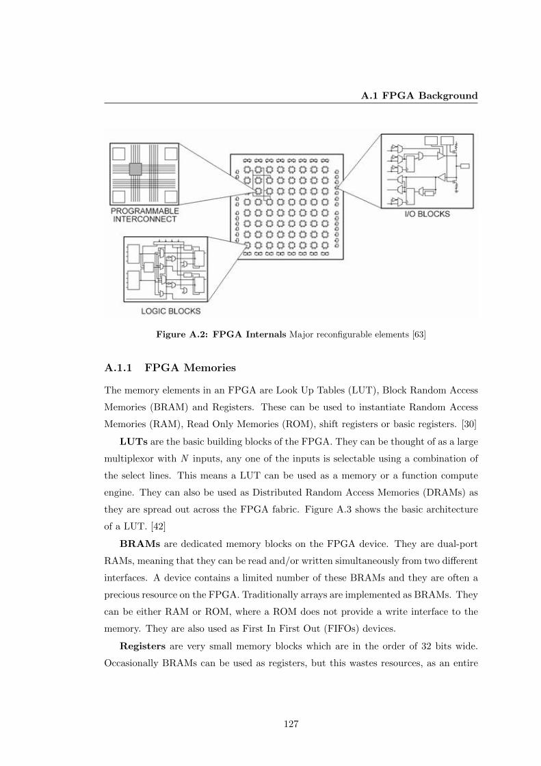
A.1 FPGA Background
Figure A.2: FPGA Internals Major reconfigurable elements [63]
A.1.1 FPGA Memories
The memory elements in an FPGA are Look Up Tables (LUT), Block Random Access
Memories (BRAM) and Registers. These can be used to instantiate Random Access
Memories (RAM), Read Only Memories (ROM), shift registers or basic registers. [30]
LUTs are the basic building blocks of the FPGA. They can be thought of as a large
multiplexor with N inputs, any one of the inputs is selectable using a combination of
the select lines. This means a LUT can be used as a memory or a function compute
engine. They can also be used as Distributed Random Access Memories (DRAMs) as
they are spread out across the FPGA fabric. Figure A.3 shows the basic architecture
of a LUT. [42]
BRAMs are dedicated memory blocks on the FPGA device. They are dual-port
RAMs, meaning that they can be read and/or written simultaneously from two different
interfaces. A device contains a limited number of these BRAMs and they are often a
precious resource on the FPGA. Traditionally arrays are implemented as BRAMs. They
can be either RAM or ROM, where a ROM does not provide a write interface to the
memory. They are also used as First In First Out (FIFOs) devices.
Registers are very small memory blocks which are in the order of 32 bits wide.
Occasionally BRAMs can be used as registers, but this wastes resources, as an entire
127
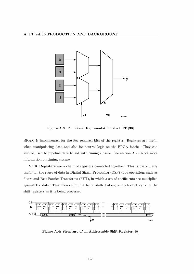
A. FPGA INTRODUCTION AND BACKGROUND
Figure A.3: Functional Representation of a LUT [30]
BRAM is implemented for the few required bits of the register. Registers are useful
when manipulating data and also for control logic on the FPGA fabric. They can
also be used to pipeline data to aid with timing closure. See section A.2.5.5 for more
information on timing closure.
Shift Registers are a chain of registers connected together. This is particularly
useful for the reuse of data in Digital Signal Processing (DSP) type operations such as
filters and Fast Fourier Transforms (FFT), in which a set of coefficients are multiplied
against the data. This allows the data to be shifted along on each clock cycle in the
shift registers as it is being processed.
Figure A.4: Structure of an Addressable Shift Register [30]
128

A.2 FPGA Design and Implementation Process
A.1.2 DSP Elements
The major components of an FPGA are BRAM blocks and logic elements (often called
different names by the different manufacturers). For example, Xilinx uses Complex
Logic Blocks (CLB) and Altera uses Logic Elements (LE). These perform similar func-
tions. [18] See A.5
The Xilinx DSP blocks in the 7 series devices are DSP48E1s. These are best used
to implement multipliers and accumulators. Among other features, they include a 25
x 18 two’s-complement multiplier and a 48 bit accumulator, each of which can be used
independently or in combination. [18] [42]
Figure A.5: Structure of a DSP48 Block [18]
A.2 FPGA Design and Implementation Process
The design of FPGAs is done using an HDL and is usually written as a modular
structure, where each module has unique functionality. The interfaces between modules
are defined as a list of Input/Output (I/O) ports. Interface where multiple modules
can communicate using a common set of I/O ports are called buses [9].
At the very basic level, designers must provide two things to the tools. First is a
description of the design logic. This is a file written in either Verilog or VHDL which
models the elements used in the design and how they are connected. The second is a set
of constraints, which tell the tools which architecture the design is targeting, the speed
of the clocks and the physical pin allocations. It can also provide more specific detail
129

A. FPGA INTRODUCTION AND BACKGROUND
such as, where to place particular registers as well as area constraints. But generally,
this can be left up to the tools.
A.2.1 HDLs (Verilog and VHDL)
An HDL is the language used to describe and model a hardware system to be imple-
mented on an FPGA or even an Application Specific Integrated Circuit (ASIC). There
are two major HDLs in widespread use, Verilog and VHDL (VHSIC (Very-High-Speed
Integrated Circuit) Hardware Definition Language). These languages differ largely in
syntax, but provide mostly similar functionality. Due to this, any choice between the
two often comes down to personal preference and the availability of simulation and
synthesis tools for a particular language. Both Altera and Xilinx provide support for
mixed language synthesis. This allows Verilog modules to be instantiated from VHDL
code and visa-versa.
HDLs provide constructs to manage the parallelism used by FPGA hardware. For
example, incoming data could be split up into X multiple parallel streams performing
the same process on the data. This means that these processes can be clocked at the
rate the data is clocked in divided by X. It is this parallelism that gives FPGAs the
power to process large amounts of data quickly.
VHDL and Verilog are good at modelling parallelised hardware, but they implement
outdated system modelling methodologies to do so. These methodologies work well
when designs are less complicated but when it comes to larger, more intricate systems
these methodologies struggle to provide the ideal tools to timeously develop and test a
system.
More recently, there is a move towards higher level languages which abstract the
designer away from the HDL level and allow easier modelling and simulation of designs.
Although, this high-level language still needs to be converted to HDL before being
passed to the synthesiser. See section 2.1.2
A.2.2 Design Constraints
The design constraint file informs the tools about which architecture and FPGA version
to compile the design for. It includes timing constraints, area constraints and physical
pin locations. The Xilinx Integrated Synthesis Environment (ISE) Design suite uses
a User Constraints File (UCF) to store the constraints. The different constraints are
130

A.2 FPGA Design and Implementation Process
used in the different stages of the compile process. Listing A.2.5 shows an example of
the Xilinx UCF file containing pin constraints.
1 // Specify that sys_clk is at 100MHz
2 Net sys_clk_n TNM_NET = sys_clk_n;
3 TIMESPEC TS_sys_clk_n = PERIOD sys_clk_n 100 MHz;
4
5 // Pin locations for sys_clk LVDS pair
6 NET "sys_clk_n" LOC = AP12;
7 NET "sys_clk_p" LOC = AP11;
8
9 // Pin locations and IO standard for GPIO pins
10 NET "v6_gpio<0>" LOC = G31 | IOSTANDARD = "LVCMOS15";
11 NET "v6_gpio<1>" LOC = H31 | IOSTANDARD = "LVCMOS15";
12 NET "v6_gpio<2>" LOC = AF32 | IOSTANDARD = "LVCMOS15";
13 NET "v6_gpio<3>" LOC = AG33 | IOSTANDARD = "LVCMOS15";
Listing 31: Xilinx UCF Example
A.2.3 Vendor Intellectual Property
Each vendor provides a tool which designers can use to generate Intellectual Property
(IP) cores. Altera Mega Wizard and Xilinx Coregen are the two supplied by the major
vendors. These are used to create IP from an existing library of cores. The libraries
include memory controllers, counters, BRAM with memory-mapped bus interfaces, to
name a few. The cores generate pre-synthesised netlists which can be included into a
design post synthesis. This is primarily to protect the vendors IP.
A.2.4 Simulation and Modelling
To ensure that each module functions as expected, a simulator is employed to test
individual modules as well as the entire system. Due to the complexity of many designs,
it is not feasible to simulate the entire design at once as this can take in the order of
hours if not days. Thus, bit-level simulation is generally only done at the module level
and a functional simulation is done at the top level.
Bit-accurate simulation comes in two flavours. Register Transfer Level (RTL) sim-
ulation in which the HDL is simulated pre-synthesis (from source). This does not
131
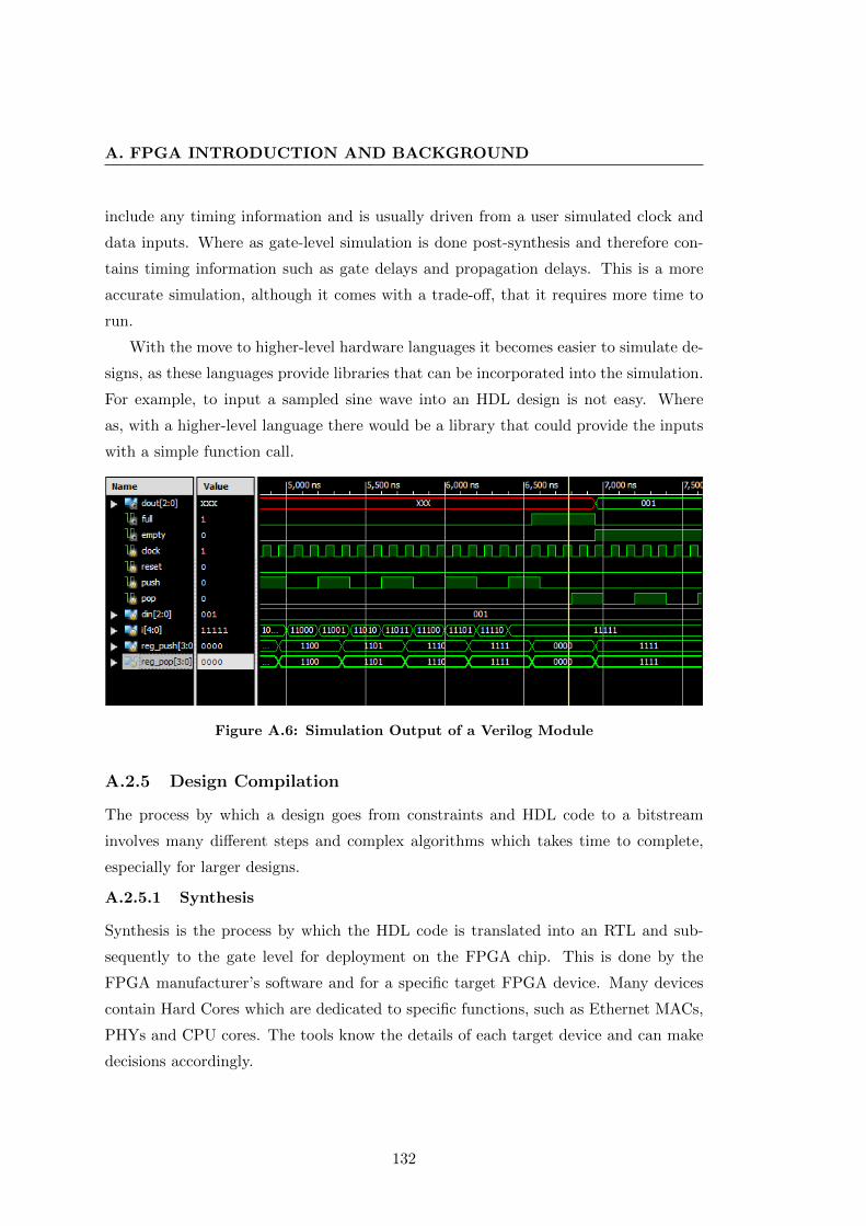
A. FPGA INTRODUCTION AND BACKGROUND
include any timing information and is usually driven from a user simulated clock and
data inputs. Where as gate-level simulation is done post-synthesis and therefore con-
tains timing information such as gate delays and propagation delays. This is a more
accurate simulation, although it comes with a trade-off, that it requires more time to
run.
With the move to higher-level hardware languages it becomes easier to simulate de-
signs, as these languages provide libraries that can be incorporated into the simulation.
For example, to input a sampled sine wave into an HDL design is not easy. Where
as, with a higher-level language there would be a library that could provide the inputs
with a simple function call.
Figure A.6: Simulation Output of a Verilog Module
A.2.5 Design Compilation
The process by which a design goes from constraints and HDL code to a bitstream
involves many different steps and complex algorithms which takes time to complete,
especially for larger designs.
A.2.5.1 Synthesis
Synthesis is the process by which the HDL code is translated into an RTL and sub-
sequently to the gate level for deployment on the FPGA chip. This is done by the
FPGA manufacturer’s software and for a specific target FPGA device. Many devices
contain Hard Cores which are dedicated to specific functions, such as Ethernet MACs,
PHYs and CPU cores. The tools know the details of each target device and can make
decisions accordingly.
132
A.2 FPGA Design and Implementation Process
A.2.5.2 Logic Optimisation
At this stage the synthesiser performs the logical optimisation on the gate level design.
It minimizes the area used on the FPGA, reduces the power consumption and ensures
timing constraints are met. It is at this stage of the compilation that certain parts of
a design can be synthesised away, particularly if its outputs are unconnected.
A.2.5.3 Mapping
The mapping stage divides the design into logic elements corresponding to the logic
cells of the FPGA. Where it can, it uses the FPGA’s built-in hard cores and the design
is mapped to the available resources on the target FPGA device.
A.2.5.4 Place and Route
The Place and Route takes the output of the map stage and places the logic elements
into logic cells as to satisfy the constraints. It connects them together attempting
to keep to the timing restrictions. For example, if a module uses a particular set of
physical FPGA I/O pins, then the logic is placed as close to the pins as possible. It
might communicate with a module on the other side of the FPGA fabric, so a middle
ground, which meets the timing requirements, needs to be found. [42]
A.2.5.5 Timing Analysis and Closure
Once the place and route is completed a timing analysis of the design takes place.
This is a crucial part of the implementation process, as issues at this stage can cause
strange errors in hardware. The purpose of timing analysis is to confirm that the placed
design can be run at the required clock frequency, under the worst case environmental
conditions without errors.
The most common timing issue is seen in synchronous systems when moving data
between registers and data is both transferred and captured using the same clock signal.
An example of this can be seen in the figure A.7. At higher clock speeds this can be
a problem, especially when the distance between registers nears the length of a clock
period. The timing diagram in figure A.7 shows how data is transmitted on the rising
edge of the first clock cycle and captured on the second rising edge. If the routing delay
of the data between the two registers is more than the time that it takes the clock edge
to propagate to the second register then the previous cycle’s data could be sampled
and stored in the second register. This is known as a race condition. [19]
133
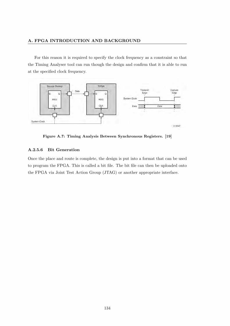
A. FPGA INTRODUCTION AND BACKGROUND
For this reason it is required to specify the clock frequency as a constraint so that
the Timing Analyser tool can run though the design and confirm that it is able to run
at the specified clock frequency.
Figure A.7: Timing Analysis Between Synchronous Registers. [19]
A.2.5.6 Bit Generation
Once the place and route is complete, the design is put into a format that can be used
to program the FPGA. This is called a bit file. The bit file can then be uploaded onto
the FPGA via Joint Test Action Group (JTAG) or another appropriate interface.
134

Appendix B
CASPER Hardware and Software
The CASPER community has a range of hardware platforms and supporting software,
which complement the tool-flow. Together, this provides a full solution for developing
radio astronomy instruments. This appendix examines the hardware and supporting
software that CASPER provides. The CASPER design tools are covered in detail in
section 2.5
B.1 CASPER Hardware
CASPER has a long history of hardware platforms from the Berkeley Emulation En-
gine 2 (BEE2) to the Interconnect Break-Out Board (IBOB) and more recently the
Reconfigurable Open Architecture Computing Hardware (ROACH) series. To keep up
with the trends in FPGAs a new board is developed with each new release of the Xilinx
Virtex FPGA range. It is this hardware that the design-flow is targeting, although
other boards can easily be incorporated into the tools. The BEE2 and the IBOB are
older hardware and have since been deprecated.
B.1.1 ROACH
The Reconfigurable Open Architecture Computing Hardware (ROACH) FPGA-based
board is designed around the Xilinx Virtex 5 FPGA. It provides four CX4 10 Gigabit
Ethernet ports, space for two Analog to Digital Converters (ADC) card slots, Dual
Data Rate 2 (DDR2) Ram, Quad Data Rate (QDR) memory and a number of other
peripherals. The board is managed by a Power Performance Computing (PowerPC)
processor which runs the Berkeley Operating system for ReProgrammable Hardware
(BOPRH) Linux. See section B.2.1 more information on BORPH.
135
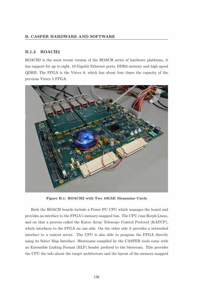
B. CASPER HARDWARE AND SOFTWARE
B.1.2 ROACH2
ROACH2 is the most recent version of the ROACH series of hardware platforms, it
has support for up to eight, 10 Gigabit Ethernet ports, DDR3 memory and high speed
QDRII. The FPGA is the Virtex 6, which has about four times the capacity of the
previous Virtex 5 FPGA.
Figure B.1: ROACH2 with Two 10GbE Mezzanine Cards
Both the ROACH boards include a Power PC CPU which manages the board and
provides an interface to the FPGA’s memory-mapped bus. The CPU runs Borph Linux,
and on that a process called the Karoo Array Telescope Control Protocol (KATCP),
which interfaces to the FPGA on one side. On the other side it provides a networked
interface to a control server. The CPU is also able to program the FPGA directly
using its Select Map Interface. Bitstreams compiled by the CASPER tools come with
an Extensible Linking Format (ELF) header prefixed to the bitstream. This provides
the CPU the info about the target architecture and the layout of the memory-mapped
136
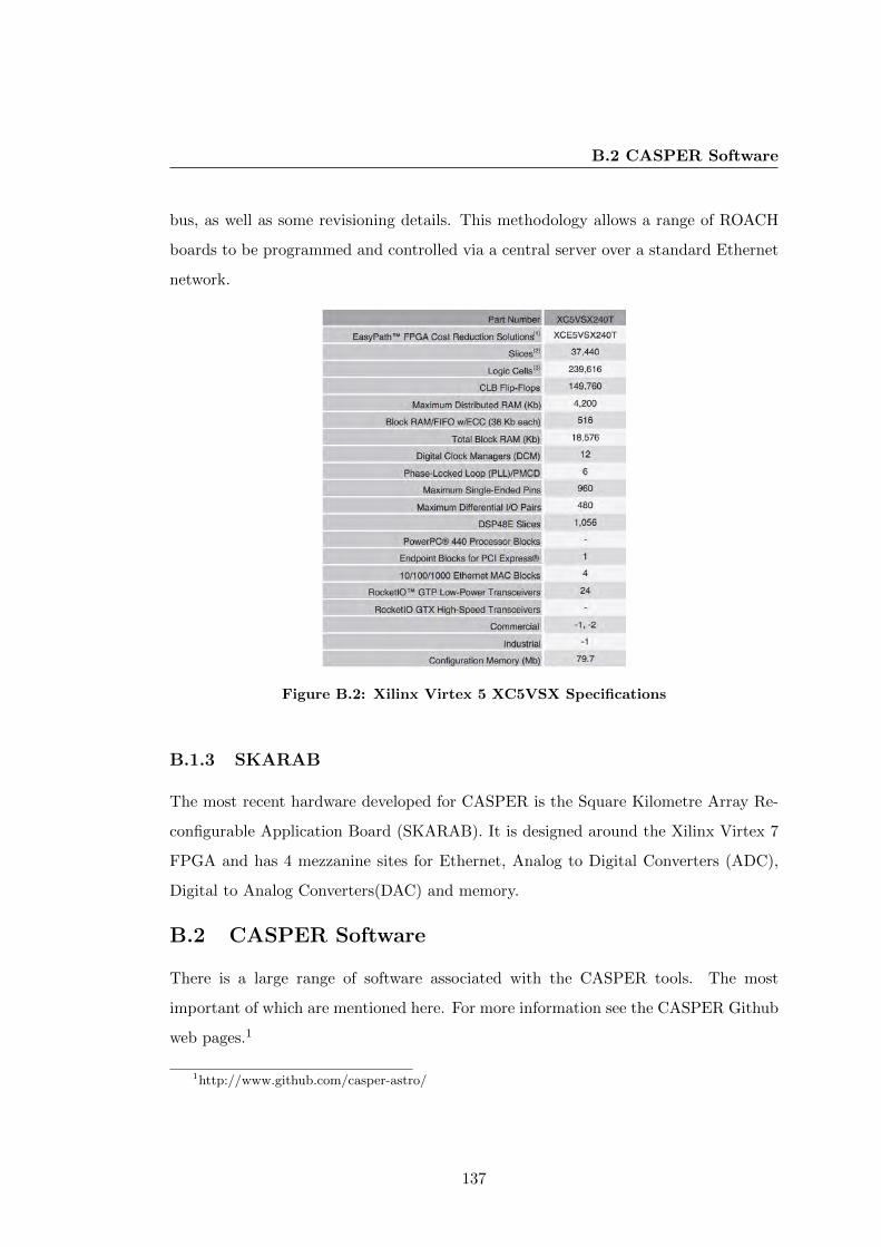
B.2 CASPER Software
bus, as well as some revisioning details. This methodology allows a range of ROACH
boards to be programmed and controlled via a central server over a standard Ethernet
network.
Figure B.2: Xilinx Virtex 5 XC5VSX Specifications
B.1.3 SKARAB
The most recent hardware developed for CASPER is the Square Kilometre Array Re-
configurable Application Board (SKARAB). It is designed around the Xilinx Virtex 7
FPGA and has 4 mezzanine sites for Ethernet, Analog to Digital Converters (ADC),
Digital to Analog Converters(DAC) and memory.
B.2 CASPER Software
There is a large range of software associated with the CASPER tools. The most
important of which are mentioned here. For more information see the CASPER Github
web pages.1
1http://www.github.com/casper-astro/
137
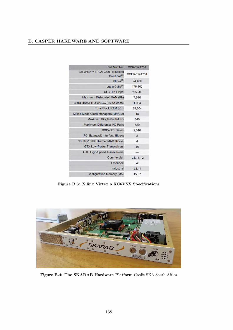
B. CASPER HARDWARE AND SOFTWARE
Figure B.3: Xilinx Virtex 6 XC6VSX Specifications
Figure B.4: The SKARAB Hardware Platform Credit SKA South Africa
138
B.2 CASPER Software
B.2.1 BORPH and U-boot
BORPH is designed to run on a processor on the FGPA board. It provides the ability to
program the FPGA over the Select Map Interface on the FPGA. This make the need for
a Joint Test Action Group (JTAG) programmer obsolete. It also allows the processor
to know where on the memory-mapped bus to read and write particular data. The
Make Borph File (MkBOF) executable appends an Extensible Linking Format (ELF)
header and the coreinfo.tab file to the bit stream. This contains the memory locations
of devices in gateware. The file is then made executable. When the processor runs this
file, the FPGA is programmed with the bit stream and the processor is able to extract
the memory allocations of the devices on the bus.
B.2.2 KATCP
KATCP is a protocol that defines a communication interface between the ROACH hard-
ware platforms and an external computer. It is used to communicate with CASPER
hardware.
B.2.3 CASPERFPGA Python Package
Casperfpga is a Python package that provides an Application Programming Interface
(API) to KATCP and an interface to program and control CASPER hardware platforms
over a network. This provides a means of reading and writing registers on the FPGA
via the networked processor on the ROACH board.
139

B. CASPER HARDWARE AND SOFTWARE
140
References
[1] J.R. Manley. A Scalable Packetised Radio Astron-
omy Imager. PHD, University of Cape Town, South
Africa, 2014. 1, 3, 4, 5, 6, 7
[2] G.E. Inggs. Putting the Pieces Together: The
Systematic Development of a Software Defined
Toolflow for the Rhino Project. Masters, University
of Cape Town, South Africa, 2011.
[3] J.R. Wyngard. An FPGA Implementation of an In-
vestigative Many-core Processor; FYNBOS. PHD,
University of Cape Town, South Africa, 2011.
[4] S. Bourdeauducq. A Performance-Driven SoC Archi-
tecture for Video Synthesis. Masters, Royal Institute
of Technology, Stockholm, 2010. 32
[5] V.K. Kodavalla. FPGA based Complex System De-
signs: Methodology and Techniques. Wipro Tech-
nologies, Bangalore, India, 2006. 2
[6] Collaboration for Astronomy Signal Processing
and Electronics Research. CASPER Website.
https://casper.berkeley.edu/wiki/, Accessed June 2014.
[7] G. Hampson et al. Xilinx FPGAs Beam Up Next-get
Radio Astronomy. EE Times, 2011. 6
[8] A. Parsons et al. A New Approach to Radio Astron-
omy Signal Procesing. CASPER White Paper, 2004. 6,
7
[9] K. Asanovic R. Bodik B. Catanzaro. The Landscape
of Parallel Computing Research: A View From
Berkeley. Technical Report, 2006. 35, 129
[10] S. Katz. Rapid Prototyping Tool for SDR on a RC
Platform. University of Cape Town, 2012.
[11] DJ Claypool, TJ McNevin, W Liu, KM McNeill. Auto-
mated Software Defined Radio Deployment Using
Domain Specific modeling Languages. IEEE Mobile
WiMAX Symposium, 2009. 29
[12] J. Delacuwe. MyHDL-based Design of a Digital
Macro. , 2010. 39
[13] J. Delacuwe. MyHDL Manual. Release 0.8, 2011. 43,
44
[14] S. Bourdeauducq. Migen Manual. Release 0.X, 2012.
32
[15] C.E. Cummings. New Verilog-2001 Techniques for
Creating Parameterized Models (or Down With
’define and Death of defparam!’). HDLCON, 2002.
[16] Xilinx Inc. Xilinx Virtex 6 Clocking Resource User
Guide 362. , 2011. 94, 95
[17] Xilinx Inc. Xilinx Virtex 6 Virtex-6 FPGA Memory
Resources User Guide 363 ver 1.8. , 2014. 84
[18] Xilinx Inc. Xilinx 7 Series DSP481E User Guide
479. , Nov 2014. 129
[19] Xilinx Inc. Xilinx Timing Closure User Guide 612.
, Nov 2012. x, 133, 134
[20] M. Hofstra. Comparing Hardware Description Lan-
guages. University of Twente, Netherlands, 2011. 40, 88
[21] . Choosing Block-Diagram Tools for DSP Design.
DSP and Multimedia Technology, 1995. 27
[22] . Choosing High-level Tools for DSP Design. DSP
and Multimedia Technology, 1996.
[23] Delite. Website. http://stanford-
ppl.github.io/Delite/optiml/index.html, Jan 2016. 27
[24] . Chisel Website. https://chisel.eecs.berkeley.edu, . 33
[25] J Bechrach et al. Chisel: Constructing Hardware in
a Scala Embedded Language. EECS Dept UC Berke-
ley, 2012. 33
[26] Wikipedia. Verilog Procedural Interface. , Aug 2015.
47
[27] IEEE 1364. Standard for Verilog Hardware Descrip-
tion Language. IEEE, 2006.
[28] S. Sutherland. The IEEE Verilog 1364-2001 Stan-
dard: What’s New, and Why You Need It. HDLCon,
2000. 21
[29] Stackoverflow. What does the
yield keyword do in Python?.
http://stackoverflow.com/questions/231767/what-does-
the-yield-keyword-do-in-python, Sept 2014. 42
[30] Xilinx. Introduction to FPGA Design with Vivado
High-Level Synthesis. Xilinx, 2013. x, 20, 23, 126, 127,
128
[31] J. Den Haan. The Enterprise Architect: Reasons
why model-driven development is dangerous.
http://www.theenterprisearchitect.eu/blog/2009/06/25/8-
reasons-why-model-driven-development-is-dangerous/,
2014. 28, 29
[32] IEEE1800-2012. IEEE Standard Unified Hardware
Design, Specification, and Verification Language.
IEEE Standards Association, 2012. 21
[33] IEEE1364-2008. IEEE Standard Verilog Hardware
Description Language. IEEE Standards Association,
2008. 47
[34] IEEE1364-2005. IEEE Standard Verilog Hardware
Description Language. IEEE Standards Association,
2005. 21
141

REFERENCES
[35] IEEE1364-2001. IEEE Standard Verilog Hardware
Description Language. IEEE Standards Association,
2001. 21
[36] IEEE1076-2008. IEEE Standard VHDL Language
Reference Manual. IEEE Standards Association, 2008.
22
[37] M. Jervis. Advances in DSP Design Tool Flows for
FPGAs. Altera Corporation, 2010.
[38] D. Dunlop. VHPI, A Programming Language In-
terface for VHDL. Cadence Design Systems Inc, 1995.
[39] Verilog HDL vs. VHDL, For the First Time User. B.
Fuchs. EE Times, 1995.
[40] A Heterogeneous Parallel Framework for Domain-
Specific Languages. K. Brown, A. Sujeeth, H. Lee,
T. Rompf, H. Chafi, M. Odersky, K. Olukotun. In-
ternational Conference on Parallel Architectures and Com-
pilation Techniques, 2011.
[41] Altera Corporation. FPGA Architecture, White Pa-
per. Altera Corporation, 2006.
[42] D. Chen, J. Cong 2, P. Pan. FPGA Design Automa-
tion: A Survey. Foundations and Trends in Electronic
Design Automation, 2006. 1, 127, 129, 133
[43] A. Poetter, P. Athanas, C. Patterson. JHDLBits. Dept
of Electrical and Computer Engineering, Virginia Polytech-
nic Institute and State University, 2005. 32
[44] F. Daitx, V. Rosa, E. Costa, P. Flores, S. Bampi. VHDL
Generation of Optimized FIR Filters. International
Conference on Signals, Circuits and Systems, 2008.
[45] CASPER. Rapid Development of Radio Astron-
omy Instrumentation Using Open Source FPGA
Boards, Tools and Libraries. , 2009. 35, 38
[46] J. Decaluwe. MyHDL - From Python to Silicon!. ,
2010. 40
[47] J. Decaluwe. MyHDL: A Python-based Hardware
Description Language. Linux Journal, 2004.
[48] J. Bromley, M. Smith. A Users Experience with Sys-
temVerilog. SNUG Europe 2004.
[49] A. Raj. High Speed and Low Power FPGA Im-
plementation of FIR Filter for DSP Applications.
SASTRA University, Thanjavur, Tamil Nadu, 2005.
[50] J. Cong et al. High-Level Synthesis for FPGAs:
From Prototyping to Deployment. IEEE Transac-
tions on Computer-Aided Design of Integrated Circuits and
Systems, VOL. 30, NO. 4, 2011. 13
[51] P. Coussy, M. Meredith, D. Gajski, A. Takach. An Intro-
duction to High-Level Synthesis. EEE Design Test
of Computers, 2009.
[52] T. Rompf, A. Sujeeth, H. Lee, K. Brown, H. Chafi, M. Oder-
sky, K. Olukotun. Building-Blocks for Performance
Oriented DSLs. EPTCS 66, 2011.
[53] A.Burg, B. Haller, E. Beck, M. Guillaud, M. Rupp, L.
Mailaender. A Rapid Prototyping Methodology for
Algorithm Development in Wireless Communica-
tions. Bell-Labs Wireless Research, Lucent Tech., 2001.
[54] J. Proakis, D. Manolakis. Digital Signal Processing.
Prentice Hall, 2006.
[55] Digital Signal Processing using FPGAs. J. Serrano.
CERN, Geneva, Switzerland, 2008.
[56] H. Andrade et al. From Streaming Models to FPGA
Implementations. ERSA12 Industrial Regular Paper,
2012.
[57] Neal K. Tibrewala, JoAnn M. Paul, and Donald E.
Thomas. Modeling and Evaluation of Hardware/-
Software Designs. Department of Electrical and Com-
puter Engineering Carnegie Mellon University Pittsburgh,
PA 15213 USA, 2001. 2
[58] S. Vernalde, P. Schaumont, I. Bolsens. An Object Ori-
ented Programming Approach for Hardware De-
sign. IMEC, Kapeldreef 75, B-3001 Leuven, Belgium,. 3,
20
[59] Joseph Kasser. The Cataract Methodology for Sys-
tems and Software Acquisition. Systems Engineering
and Evaluation Centre University of South Australia, 2002.
ix, 10, 11, 55
[60] Pong P. Chu. Verilog Prototyping by Verilog Exam-
ples. Wiley, 2008. 19
[61] James E. Stine. Digital Computer Arithmetic Dat-
apath Design Using Verilog HDL. Kluwer Academic
Publishers, 2004. 21
[62] Dr. H. Abdullah, H. Hadi. Design and Implementa-
tion of FPGA based Software Defined Radio using
Simulink HDL Coder. University of Al-Mustansiryah,
College of Engineering, 2009. 31
[63] National Instruments. FPGA Fundamentals.
http://www.ni.com/white-paper/6983/en/, 2012. 125, 127
[64] Stanford University Pervasive Parallelism Laboratory. .
https://ppl.stanford.edu/projects, June 2014. 28
[65] A. Parsons, et al. A New Approach to Radio
Astronomy Signal Processing: Packet Switched,
FPGA-based, Upgradeable, Modular Hardware
and Reusable, Platform-Independent Signal Pro-
cessing Libraries. CASPER Paper, 2005. 7
[66] P. McMahon, et al. Adventures in Radio Astron-
omy Instrumentation and Signal Processing. Mas-
ters, University of Cape Town, South Africa, 2008. 7
142