Embed Size (px)
Citation preview
AE108/AC108/AT108 MICROPROCESSORS & MICROCONTROLLERS DEC 2014
© IETE 1
Q.2 a. Discuss and differentiate between a Microprocessor and a Microcontroller.
Answer: Microprocessor is an IC which has only the CPU inside them i.e. only the processing powers such as Intel’s Pentium 1,2,3,4, core 2 duo, i3, i5 etc. These microprocessors don’t have RAM, ROM, and other peripheral on the chip. A system designer has to add them externally to make them functional. Application of microprocessor includes Desktop PC’s, Laptops, notepads etc. But this is not the case with Microcontrollers. Microcontroller has a CPU, in addition with a fixed amount of RAM, ROM and other peripherals all embedded on a single chip. At times it is also termed as a mini computer or a computer on a single chip. Today different manufacturers produce microcontrollers with a wide range of features available in different versions. Some manufacturers are ATMEL, Microchip, TI, Freescale, Philips, Motorola etc. Microcontrollers are designed to perform specific tasks. Specific means applications where the relationship of input and output is defined. Depending on the input, some processing needs to be done and output is delivered. For example, keyboards, mouse, washing machine, digicam, pendrive, remote, microwave, cars, bikes, telephone, mobiles, watches, etc. Since the applications are very specific, they need small resources like RAM, ROM, I/O ports etc and hence can be embedded on a single chip. This in turn reduces the size and the cost. Microprocessor find applications where tasks are unspecific like developing software, games, websites, photo editing, creating documents etc. In such cases the relationship between input and output is not defined. They need high amount of resources like RAM, ROM, I/O ports etc. The clock speed of the Microprocessor is quite high as compared to the microcontroller. Whereas the microcontrollers operate from a few MHz to 30 to 50 MHz, today’s microprocessor operate above 1GHz as they perform complex tasks. Comparing microcontroller and microprocessor in terms of cost is not justified. Undoubtedly a microcontroller is far cheaper than a microprocessor. However microcontroller cannot be used in place of microprocessor and using a microprocessor is not advised in place of a microcontroller as it makes the application quite costly. Microprocessor cannot be used stand alone. They need other peripherals like RAM, ROM, buffer, I/O ports etc and hence a system designed around a microprocessor is quite costly. b. List different system buses of 8085 microprocessor and give function of
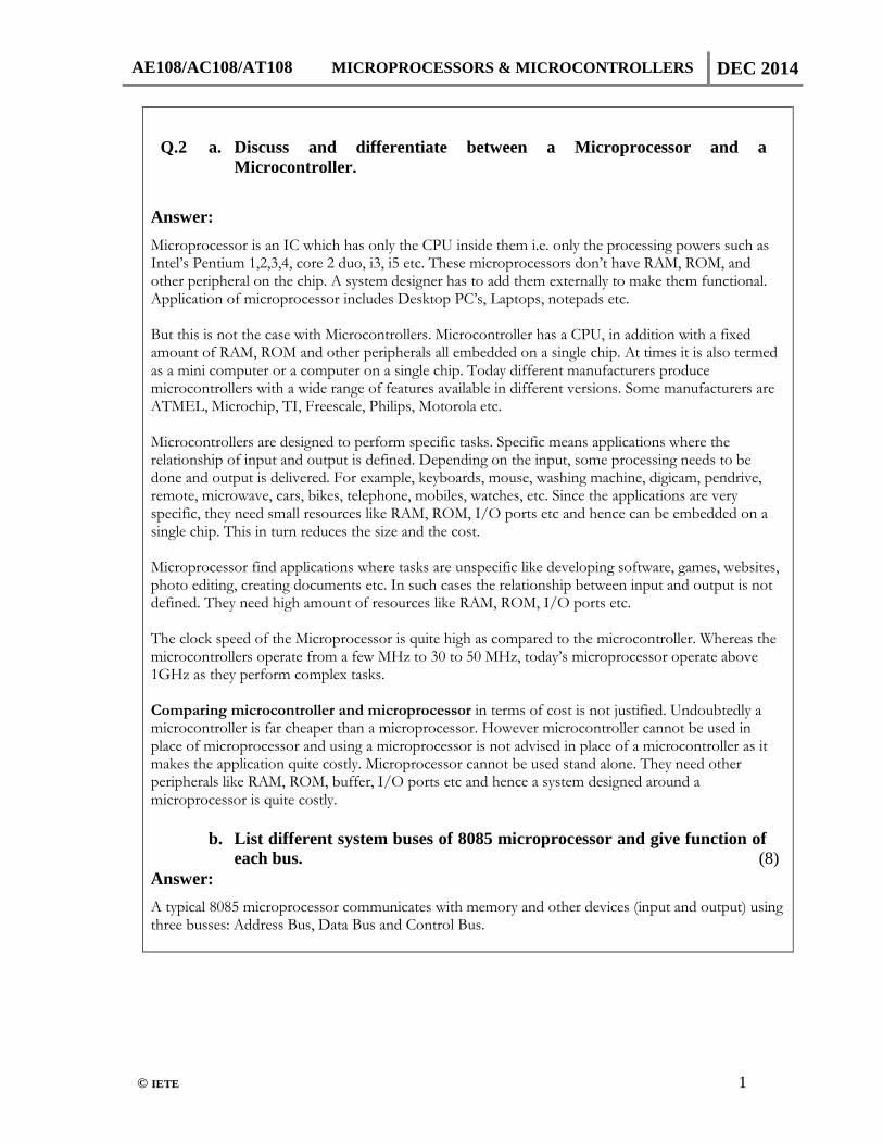
each bus. (8) Answer: A typical 8085 microprocessor communicates with memory and other devices (input and output) using three busses: Address Bus, Data Bus and Control Bus.
AE108/AC108/AT108 MICROPROCESSORS & MICROCONTROLLERS DEC 2014
© IETE 2
Address Bus One wire for each bit, therefore 16 bits = 16 wires. Binary number carried alerts memory to ‘open’ the designated box. Data (binary) can then be put in or taken out.The Address Bus consists of 16 wires, therefore 16 bits. Its "width" is 16 bits. A 16 bit binary number allows 216 different numbers, or 32000 different numbers, ie 0000000000000000 up to 1111111111111111. Because memory consists of boxes, each with a unique address, the size of the address bus determines the size of memory, which can be used. To communicate with memory the microprocessor sends an address on the address bus, eg 0000000000000011 (3 in decimal), to the memory. The memory the selects box number 3 for reading or writing data. Address bus is unidirectional, ie numbers only sent from microprocessor to memory, not other way. Data Bus Data Bus: carries ‘data’, in binary form, between μP and other external units, such as memory. Typical size is 8 or 16 bits. Size determined by size of boxes in memory and μP size helps determine performance of μP. The Data Bus typically consists of 8 wires. Therefore, 28 combinations of binary digits. Data bus used to transmit "data", ie information, results of arithmetic, etc, between memory and the microprocessor. Bus is bi-directional. Size of the data bus determines what arithmetic can be done. If only 8 bits wide then largest number is 11111111 (255 in decimal). Therefore, larger number have to be broken down into chunks of 255. This slows microprocessor. Data Bus also carries instructions from memory to the microprocessor. Size of the bus therefore limits the number of possible instructions to 256, each specified by a separate number. Control Bus Control Bus are various lines which have specific functions for coordinating and controlling uP operations. Eg: Read/NotWrite line, single binary digit. Control whether memory is being ‘written to’ (data stored in mem) or ‘read from’ (data taken out of mem) 1 = Read, 0 = Write. May also include clock line(s) for timing/synchronising, ‘interrupts’, ‘reset’ etc. Typically μP has 10 control lines. Cannot function correctly without these vital control signals. The Control Bus carries control signals partly unidirectional, partly bi-directional. Control signals are things like "read or write". This tells memory that we are either reading from a location, specified on the address bus, or writing to a location specified. Various other signals to control and coordinate the operation of the system. Modern day microprocessors, like 80386, 80486 have much larger busses. Typically 16 or 32 bit busses, which allow larger number of instructions, more memory
AE108/AC108/AT108 MICROPROCESSORS & MICROCONTROLLERS DEC 2014
© IETE 3
location, and faster arithmetic. Microcontrollers organized along same lines, except: because microcontrollers have memory etc inside the chip, the busses may all be internal. In the microprocessor the three busses are external to the chip (except for the internal data bus). In case of external busses, the chip connects to the busses via buffers, which are simply an electronic connection between external bus and the internal data bus. Q.3 a. Discuss in detail the isolated I/O mapping and memory mapped I/O
devices.
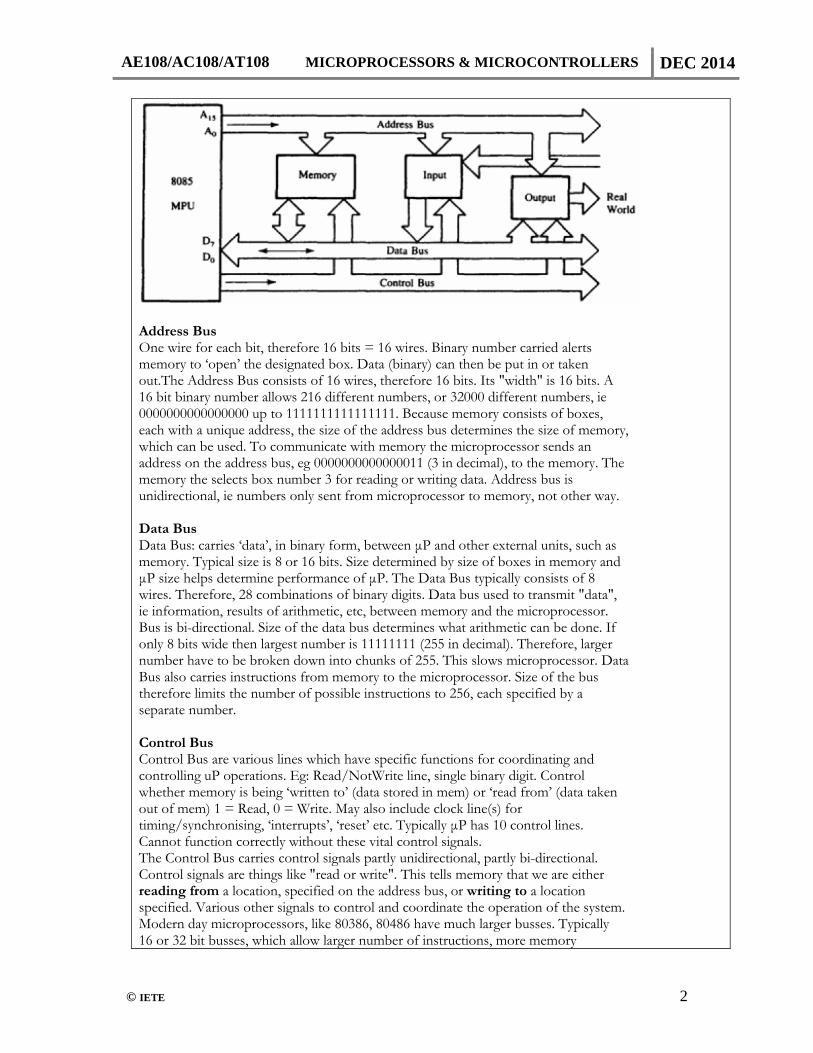
Answer: There are two types for interfacing I/O devices: 1. Memory mapped I/O device. 2. Standard I/O mapped I/O device or isolated I/O mapping.
b. Let at the program memory location 4080, the instruction MOV B, A
(opcode 47H) is stored while the accumulator content is FFH. Illustrate the execution of this instruction by timing diagram.
Answer:
AE108/AC108/AT108 MICROPROCESSORS & MICROCONTROLLERS DEC 2014
© IETE 4
Q.4 a. Write a program in 8085 assembly language to convert BCD to Binary.
Answer:
b. Write a program in 8085 assembly language to multiply two numbers.
Answer:
AE108/AC108/AT108 MICROPROCESSORS & MICROCONTROLLERS DEC 2014
© IETE 5
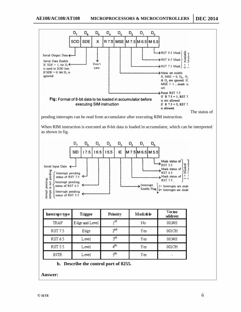
Q.5 a. Explain RIM ,SIM instructions with suitable illustration. (8) Answer: SIM and RIM for interrupts: The 8085 provide additional masking facility for RST 7.5, RST 6.5 and RST 5.5 using SIM instruction. The status of these interrupts can be read by executing RIM instruction. The masking or unmasking of RST 7.5, RST 6.5 and RST 5.5 interrupts can be performed by moving an 8-bit data to accumulator and then executing SIM instruction. The format of the 8-bit data is shown below.
AE108/AC108/AT108 MICROPROCESSORS & MICROCONTROLLERS DEC 2014
© IETE 6
The status of pending interrupts can be read from accumulator after executing RIM instruction. When RIM instruction is executed an 8-bit data is loaded in accumulator, which can be interpreted as shown in fig.
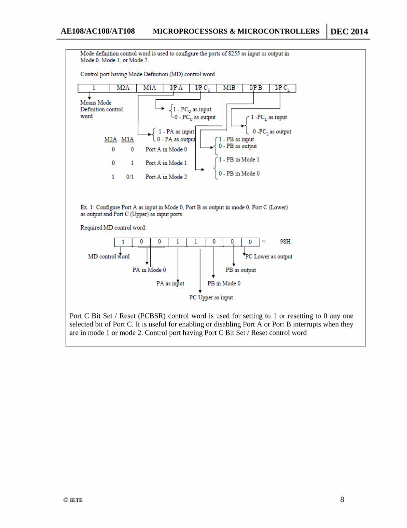
b. Describe the control port of 8255. Answer:
AE108/AC108/AT108 MICROPROCESSORS & MICROCONTROLLERS DEC 2014
© IETE 7
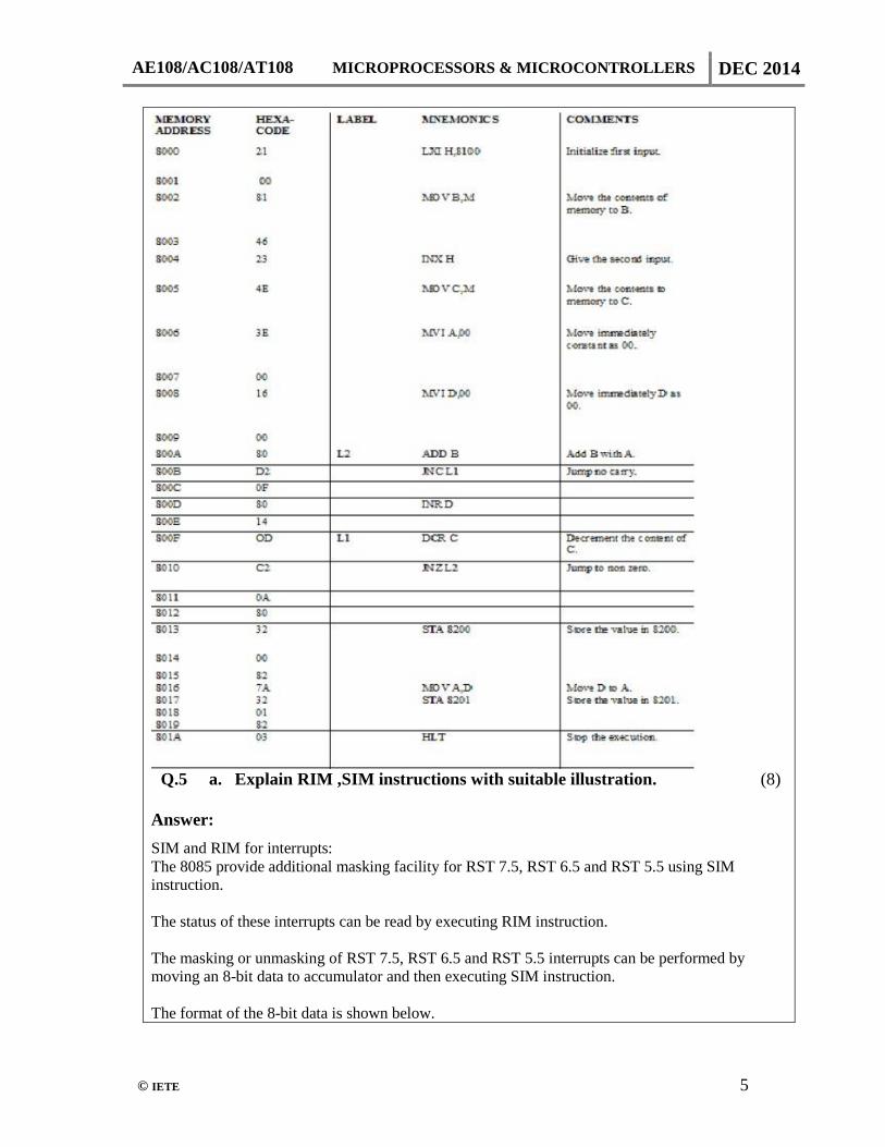
A1 A0 Selected port 0 0 Port A 0 1 Port B 1 0 Port C 1 1 Control port The Control port contents decides the working of 8255. When CS (Chip select) is 0, 8255 is selected for communication by the processor. The chip select circuit connected to the CS pin assigns addresses to the ports of 8255.For the chip select circuit shown, the chip is selected when A7=0, A6=1, A5=1, A4=1, A3=1, A2=1, and M/IO*= 0. Port A, Port B, Port C and Control port will have the addresses as 7CH, 7DH, 7EH, and 7FH respectively.
AE108/AC108/AT108 MICROPROCESSORS & MICROCONTROLLERS DEC 2014
© IETE 8
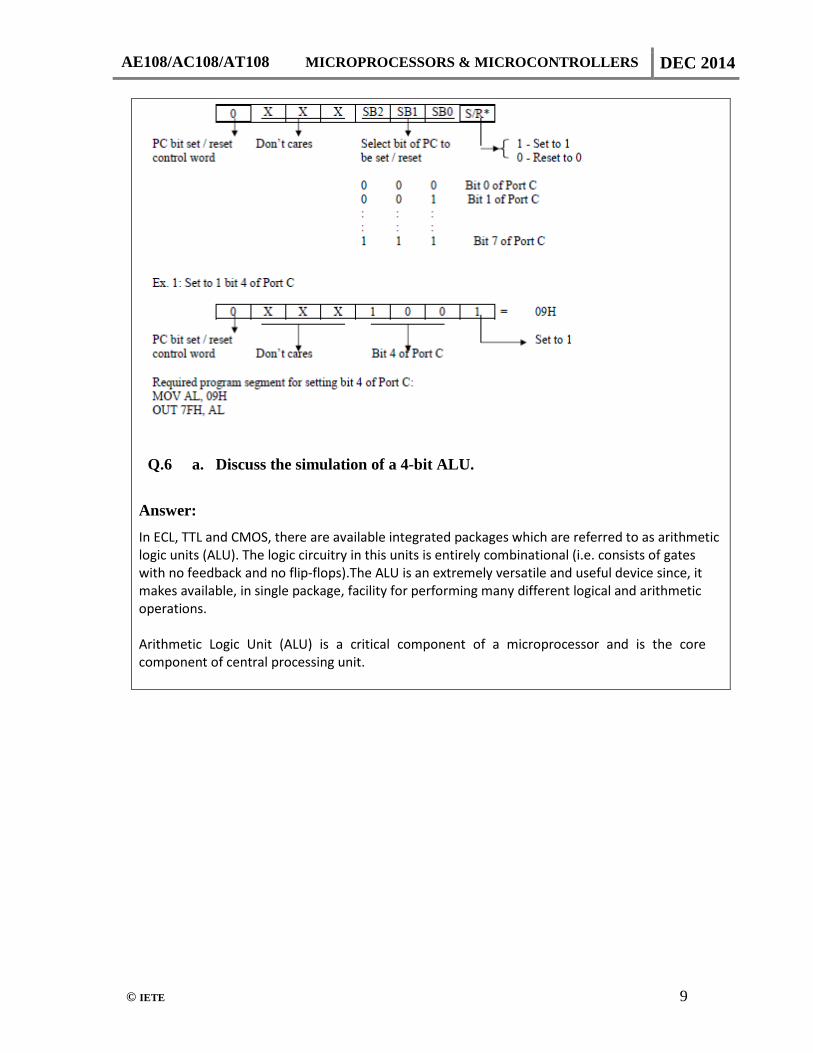
Port C Bit Set / Reset (PCBSR) control word is used for setting to 1 or resetting to 0 any one selected bit of Port C. It is useful for enabling or disabling Port A or Port B interrupts when they are in mode 1 or mode 2. Control port having Port C Bit Set / Reset control word
AE108/AC108/AT108 MICROPROCESSORS & MICROCONTROLLERS DEC 2014
© IETE 9
Q.6 a. Discuss the simulation of a 4-bit ALU.
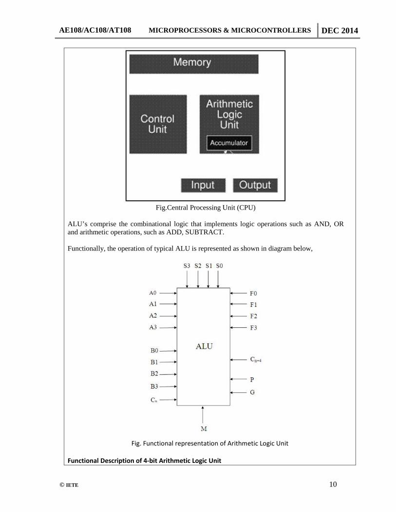
Answer: In ECL, TTL and CMOS, there are available integrated packages which are referred to as arithmetic logic units (ALU). The logic circuitry in this units is entirely combinational (i.e. consists of gates with no feedback and no flip-flops).The ALU is an extremely versatile and useful device since, it makes available, in single package, facility for performing many different logical and arithmetic operations. Arithmetic Logic Unit (ALU) is a critical component of a microprocessor and is the core component of central processing unit.
AE108/AC108/AT108 MICROPROCESSORS & MICROCONTROLLERS DEC 2014
© IETE 10
Fig.Central Processing Unit (CPU)
ALU’s comprise the combinational logic that implements logic operations such as AND, OR and arithmetic operations, such as ADD, SUBTRACT. Functionally, the operation of typical ALU is represented as shown in diagram below,
Fig. Functional representation of Arithmetic Logic Unit
Functional Description of 4-bit Arithmetic Logic Unit
AE108/AC108/AT108 MICROPROCESSORS & MICROCONTROLLERS DEC 2014
© IETE 11
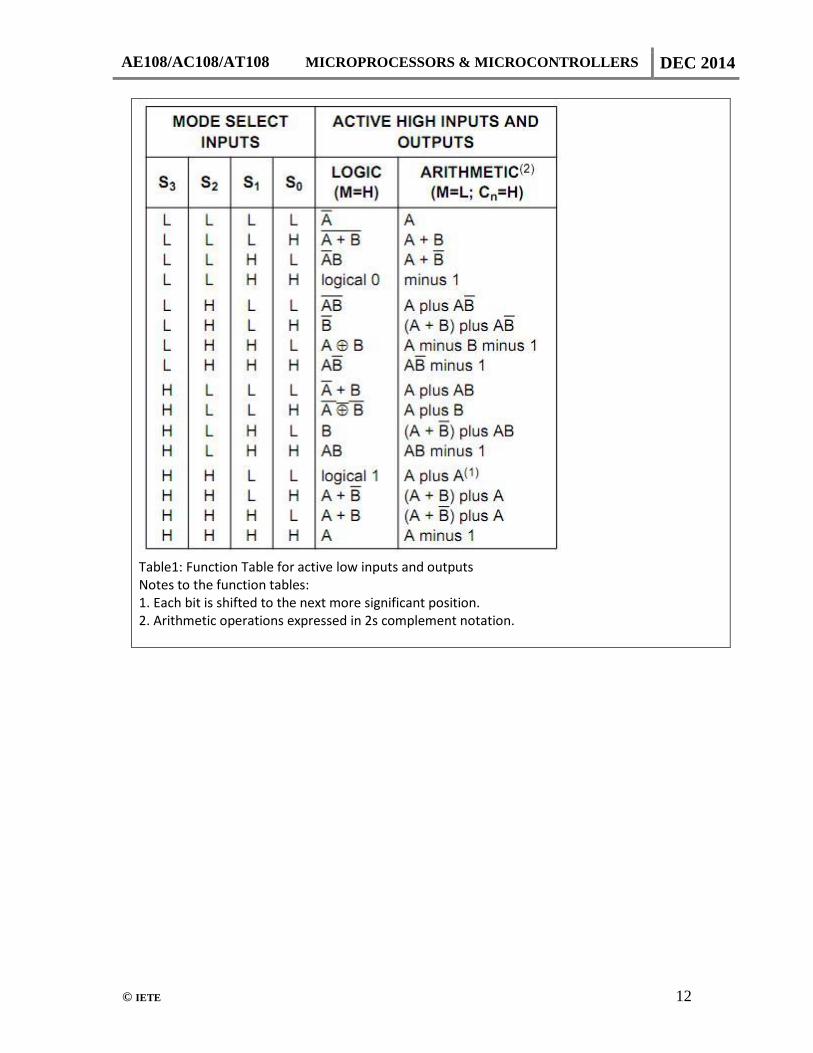
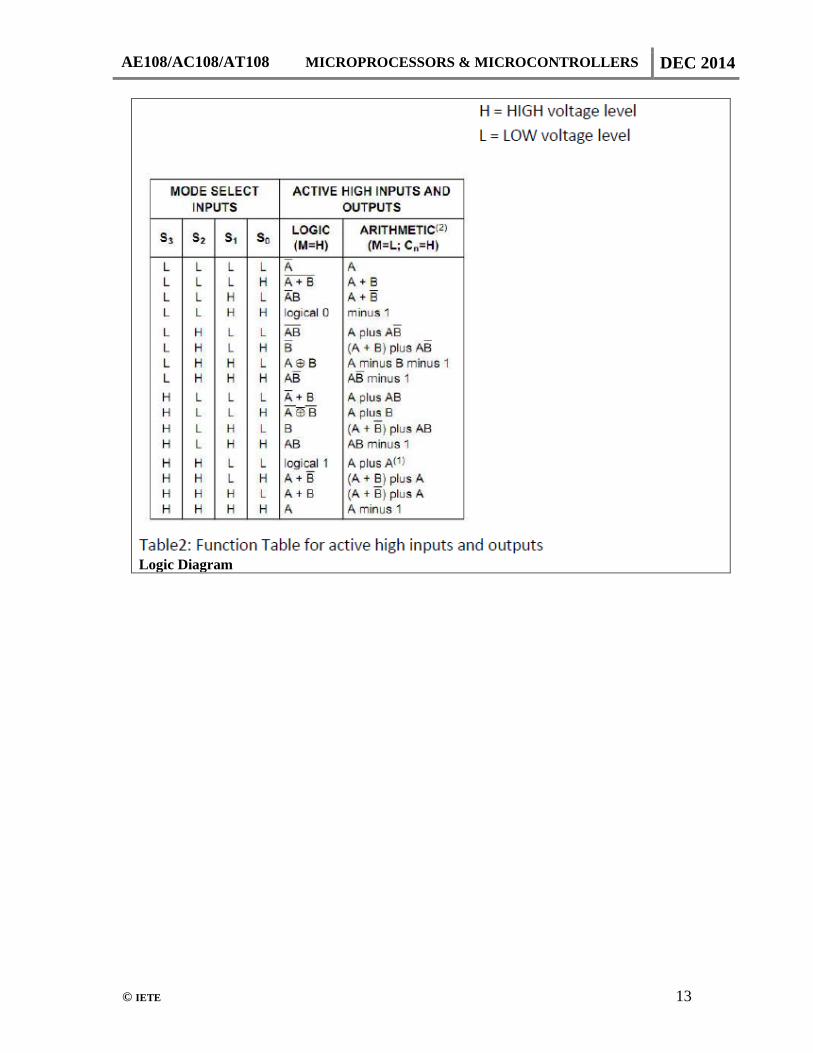
Controlled by the four function select inputs (S0 to S3) and the mode control input (M), ALU can perform all the 16 possible logic operations or 16 different arithmetic operations on active HIGH or active LOW operands. When the mode control input (M) is HIGH, all internal carries are inhibited and the device performs logic operations on the individual bits. When M is LOW, the carries are enabled and the ALU performs arithmetic operations on the two 4-bit words. The ALU incorporates full internal carry look-ahead and provides for either ripple carry between devices using the Cn+4 output, or for carry look-ahead between packages using the carry propagation (P) and carry generate (G) signals. P and G are not affected by carry in. For high-speed operation the device is used in conjunction with the ALU carry look-ahead circuit. One carry look-ahead package is required for each group of four ALU devices. Carry look-ahead can be provided at various levels and offers high-speed capability over extremely long word lengths. The comparator output (A=B) of the device goes HIGH when all four function outputs (F0 to F3) are HIGH and can be used to indicate logic equivalence over 4 bits when the unit is in the subtract mode. A=B is an open collector output and can be wired-AND with other A=B outputs to give a comparison for more than 4 bits. The open drain output A=B should be used with an external pull-up resistor in order to establish a logic HIGH level. The A=B signal can also be used with the Cn+4 signal to indicate A > B and A < B. The function table lists the arithmetic operations that are performed without a carry in. An incoming carry adds a one to each operation. Thus, select code LHHL generates A minus B minus 1 (2s complement notation) without a carry in and generates A minus B when a carry is applied. Because subtraction is actually performed by complementary addition (1s complement), a carry out means borrow; thus, a carry is generated when there is no under-flow and no carry is generated when there is underflow. As indicated, the ALU can be used with either active LOW inputs producing active LOW outputs (Table 1) or with active HIGH inputs producing active HIGH outputs (Table 2).
AE108/AC108/AT108 MICROPROCESSORS & MICROCONTROLLERS DEC 2014
© IETE 12
Table1: Function Table for active low inputs and outputs Notes to the function tables: 1. Each bit is shifted to the next more significant position. 2. Arithmetic operations expressed in 2s complement notation.
AE108/AC108/AT108 MICROPROCESSORS & MICROCONTROLLERS DEC 2014
© IETE 13
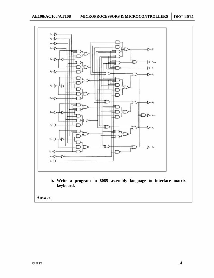
Logic Diagram
AE108/AC108/AT108 MICROPROCESSORS & MICROCONTROLLERS DEC 2014
© IETE 14
b. Write a program in 8085 assembly language to interface matrix
keyboard.
Answer:
AE108/AC108/AT108 MICROPROCESSORS & MICROCONTROLLERS DEC 2014
© IETE 15
Q.7 a. How do the 8259A accomplish the interrupt activity?
Answer: The device requiring service signals the PIC via one of the seven PIC interrupt request (IR) input lines. The corresponding bit in the PIC Interrupt Request register (IIR) is set.
• The PIC activates the INT line which is connected to the CPU INTR line.
• If the interrupts are not masked at the CPU, it finishes the currently executing instruction and sends one interrupt acknowledge (INTA) pulse to the PIC.
• In an X85 environment, the PIC responds by setting the highest priority In Service Register (ISR) bit and the corresponding IIR bit is reset. There is no PIC activity on the data bus in this cycle.
AE108/AC108/AT108 MICROPROCESSORS & MICROCONTROLLERS DEC 2014
© IETE 16
• The CPU will initiate a second INTA pulse. During this pulse, the PIC releases an 8-bit pointer on to the data bus where it is read by the CPU.
• The CPU reads the interrupt-type number, determines the associated address of the interrupt service routine (ISR), then fetches and executes the ISR.
• In the Automatic End Of Interrupt (AEOI) Mode the ISR bit is reset at the end of the second INTA pulse. Otherwise the ISR bit remains set until an appropriate EOI command is issued at the end of the ISR.
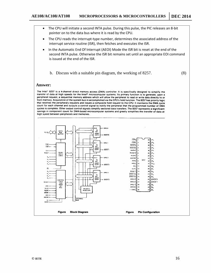
b. Discuss with a suitable pin diagram, the working of 8257. (8)
Answer:
AE108/AC108/AT108 MICROPROCESSORS & MICROCONTROLLERS DEC 2014
© IETE 17
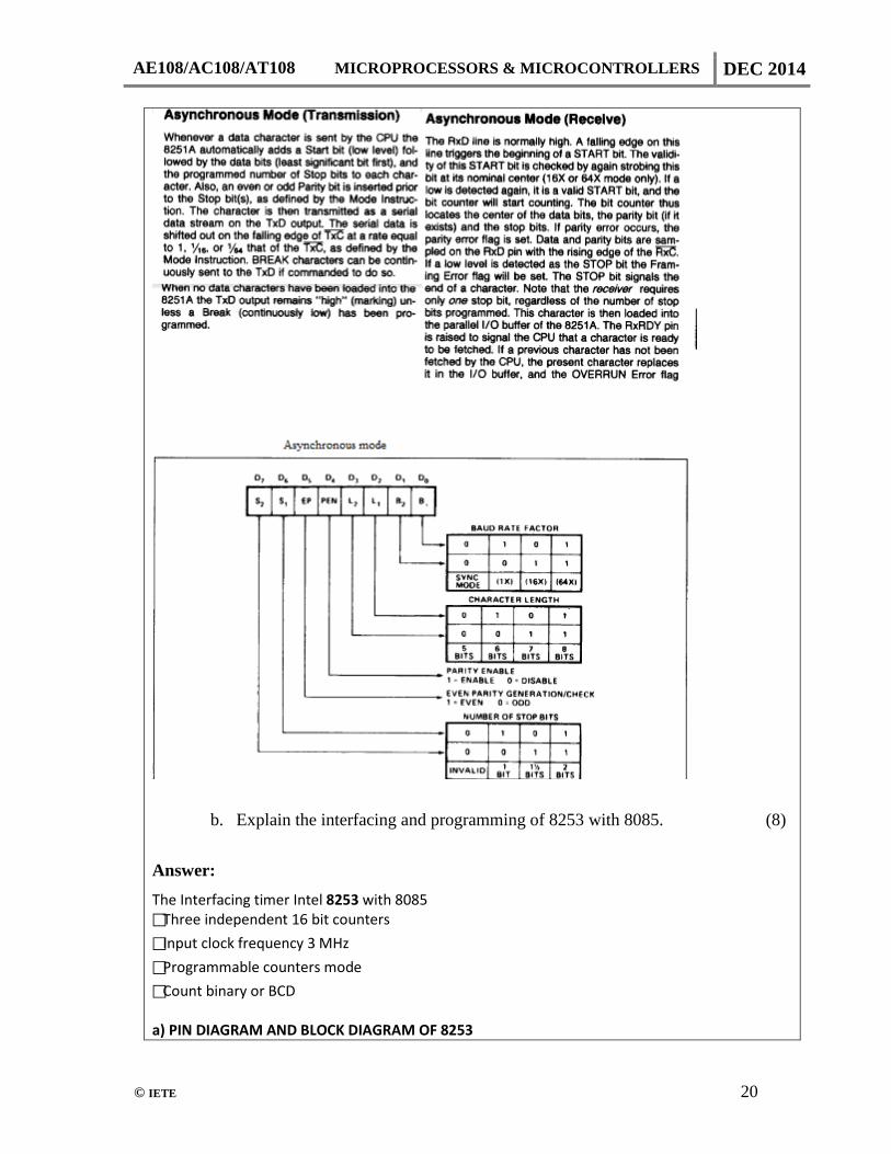
Q.8 a. Explain asynchronous transmission using 8251.
Answer:
AE108/AC108/AT108 MICROPROCESSORS & MICROCONTROLLERS DEC 2014
© IETE 18
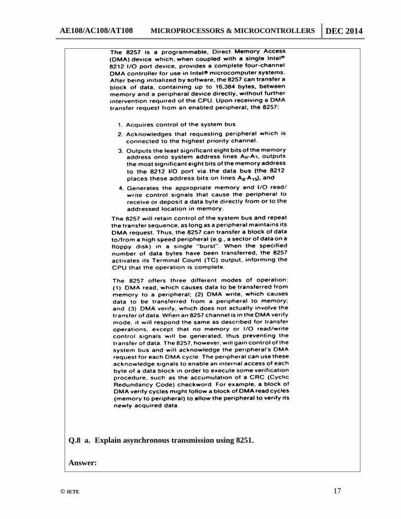
The 8251 is a USART (Universal Synchronous Asynchronous Receiver Transmitter) for serial data communication. As a peripheral device of a microcomputer system, the 8251 receives parallel data from the CPU and transmits serial data after conversion. This device also receives serial data from the outside and transmits parallel data to the CPU after conversion.
Block diagram of the 8251 USART (Universal Synchronous Asynchronous Receiver Transmitter) The 8251 functional configuration is programed by software. Operation between the 8251 and a CPU is executed by program control. Table 1 shows the operation between a CPU and the device.
AE108/AC108/AT108 MICROPROCESSORS & MICROCONTROLLERS DEC 2014
© IETE 19
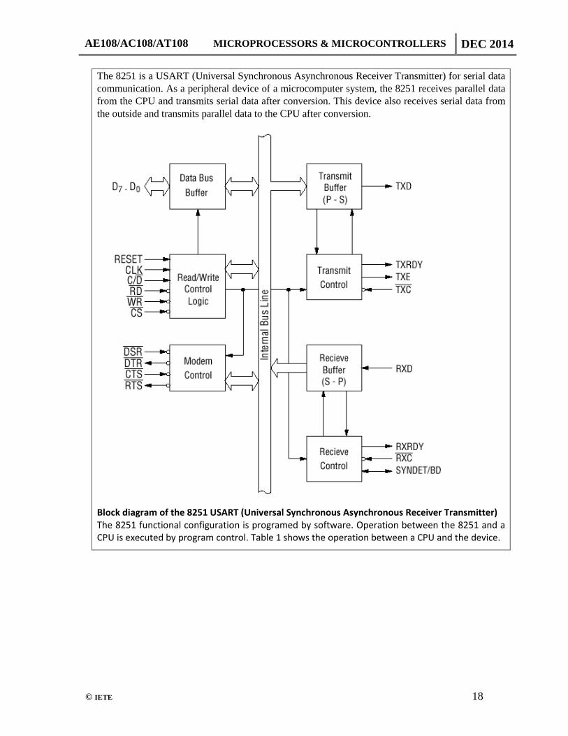
Table Operation between a CPU and 8251
Control Words There are two types of control word. 1. Mode instruction (setting of function) 2. Command (setting of operation) 1) Mode Instruction Mode instruction is used for setting the function of the 8251. Mode instruction will be in "wait for write" at either internal reset or external reset. That is, the writing of a control word after resetting will be recognized as a "mode instruction." Items set by mode instruction are as follows: • Synchronous/asynchronous mode • Stop bit length (asynchronous mode) • Character length • Parity bit • Baud rate factor (asynchronous mode) • Internal/external synchronization (synchronous mode) • Number of synchronous characters (Synchronous mode)
AE108/AC108/AT108 MICROPROCESSORS & MICROCONTROLLERS DEC 2014
© IETE 20
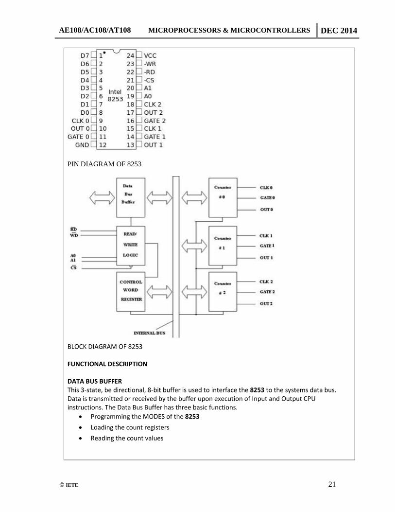
b. Explain the interfacing and programming of 8253 with 8085. (8)
Answer: The Interfacing timer Intel 8253 with 8085 Three independent 16 bit counters Input clock frequency 3 MHz Programmable counters mode Count binary or BCD a) PIN DIAGRAM AND BLOCK DIAGRAM OF 8253
AE108/AC108/AT108 MICROPROCESSORS & MICROCONTROLLERS DEC 2014
© IETE 21
PIN DIAGRAM OF 8253
BLOCK DIAGRAM OF 8253 FUNCTIONAL DESCRIPTION DATA BUS BUFFER This 3-state, be directional, 8-bit buffer is used to interface the 8253 to the systems data bus. Data is transmitted or received by the buffer upon execution of Input and Output CPU instructions. The Data Bus Buffer has three basic functions.
• Programming the MODES of the 8253 • Loading the count registers • Reading the count values
AE108/AC108/AT108 MICROPROCESSORS & MICROCONTROLLERS DEC 2014
© IETE 22
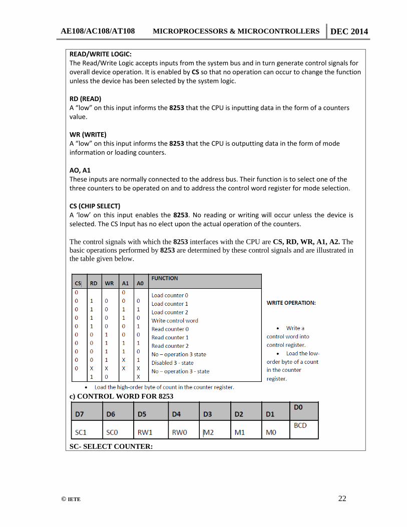
READ/WRITE LOGIC: The Read/Write Logic accepts inputs from the system bus and in turn generate control signals for overall device operation. It is enabled by CS so that no operation can occur to change the function unless the device has been selected by the system logic. RD (READ) A “low” on this input informs the 8253 that the CPU is inputting data in the form of a counters value. WR (WRITE) A “low” on this input informs the 8253 that the CPU is outputting data in the form of mode information or loading counters. AO, A1 These inputs are normally connected to the address bus. Their function is to select one of the three counters to be operated on and to address the control word register for mode selection. CS (CHIP SELECT) A ‘low’ on this input enables the 8253. No reading or writing will occur unless the device is selected. The CS Input has no elect upon the actual operation of the counters. The control signals with which the 8253 interfaces with the CPU are CS, RD, WR, A1, A2. The basic operations performed by 8253 are determined by these control signals and are illustrated in the table given below.
c) CONTROL WORD FOR 8253
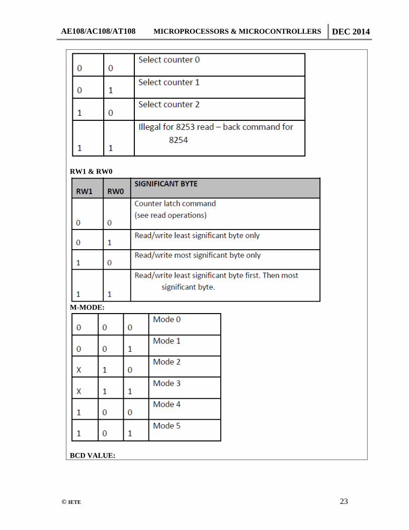
SC- SELECT COUNTER:
AE108/AC108/AT108 MICROPROCESSORS & MICROCONTROLLERS DEC 2014
© IETE 23
RW1 & RW0
M-MODE:
BCD VALUE:
AE108/AC108/AT108 MICROPROCESSORS & MICROCONTROLLERS DEC 2014
© IETE 24
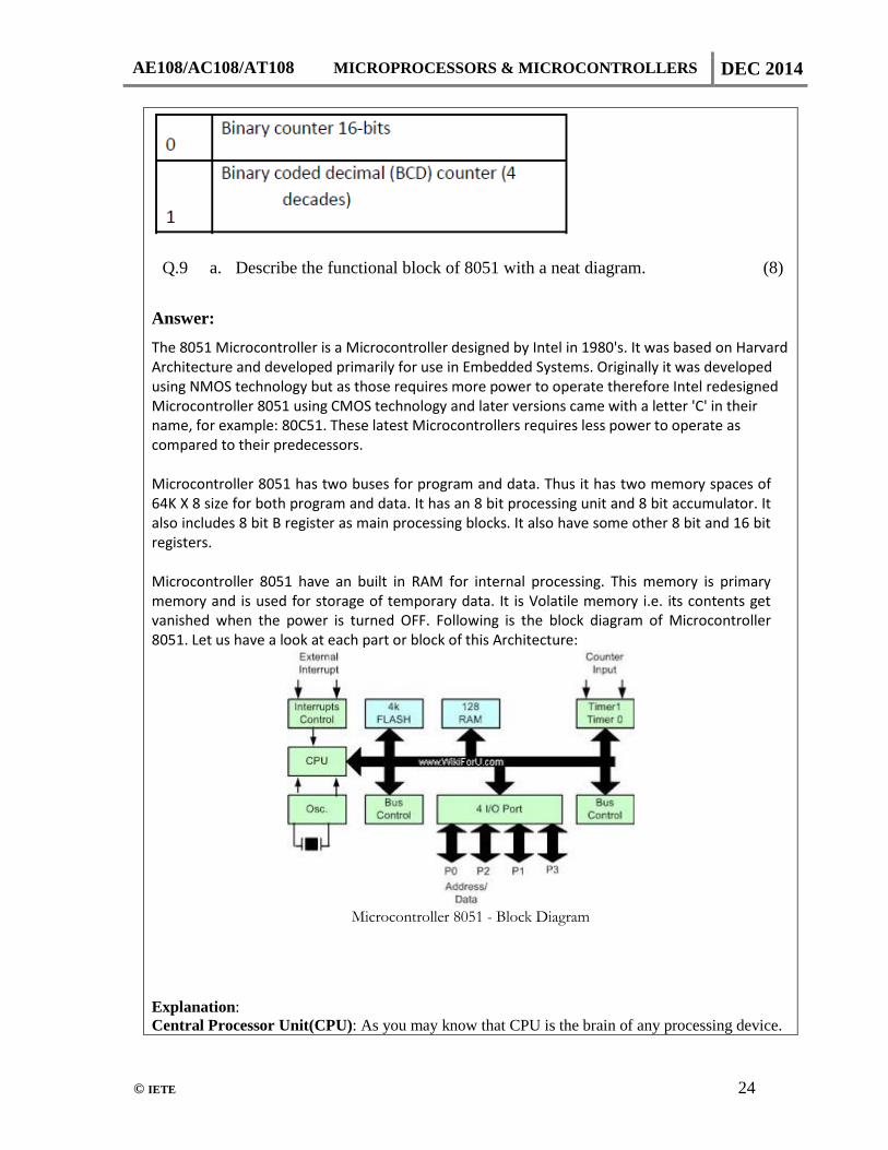
Q.9 a. Describe the functional block of 8051 with a neat diagram. (8)
Answer: The 8051 Microcontroller is a Microcontroller designed by Intel in 1980's. It was based on Harvard Architecture and developed primarily for use in Embedded Systems. Originally it was developed using NMOS technology but as those requires more power to operate therefore Intel redesigned Microcontroller 8051 using CMOS technology and later versions came with a letter 'C' in their name, for example: 80C51. These latest Microcontrollers requires less power to operate as compared to their predecessors. Microcontroller 8051 has two buses for program and data. Thus it has two memory spaces of 64K X 8 size for both program and data. It has an 8 bit processing unit and 8 bit accumulator. It also includes 8 bit B register as main processing blocks. It also have some other 8 bit and 16 bit registers. Microcontroller 8051 have an built in RAM for internal processing. This memory is primary memory and is used for storage of temporary data. It is Volatile memory i.e. its contents get vanished when the power is turned OFF. Following is the block diagram of Microcontroller 8051. Let us have a look at each part or block of this Architecture:
Microcontroller 8051 - Block Diagram
Explanation: Central Processor Unit(CPU): As you may know that CPU is the brain of any processing device.
AE108/AC108/AT108 MICROPROCESSORS & MICROCONTROLLERS DEC 2014
© IETE 25
It monitors and controls all operations that are performed in the Microcontroller. User have no control over the work of CPU. It reads program written in ROM memory and executes them and do the expected task. Interrupts: As its name suggests, Interrupt is a subroutine call that interrupts Microcontroller's main operation or work and causes it to execute some another program which is more important at that time. The feature of Interrupt is very useful as it helps in cases of emergency. Interrupts gives us a mechanism to put on hold the ongoing operation , execute a subroutine and then again resumes normal program execution. The Microcontroller 8051 can be configured in such a way that it temporarily terminates or pause the main program at the occurrence of interrupt. When subroutine is completed then the execution of main program starts as usual. There are five interrupt sources in 8051 Microcontroller. 2 of them are external interrupts, 2 timer interrupts and one serial port interrupt. Memory: Microcontroller requires a program which is a collection of instructions. This program tells Microcontroller to do specific tasks. These programs requires a memory on which these can be saved and read by Microcontroller to perform specific operation. The memory which is used to store the program of Microcontroller, is known as code memory or Program memory . It is known as 'ROM'(Read Only Memory). Microcontroller also requires a memory to store data or operands temporarily. The memory which is used to temporarily store data for operation is known as Data Memory and we uses 'RAM'(Random Access Memory) for this purpose. Microcontroller 8051 has 4K of Code Memory or Program memory that is it has 4KB Rom and it also have 128 bytes of data memory i.e. RAM. Bus: Basically Bus is a collection of wires which work as a communication channel or medium for transfer of Data. These buses consists of 8, 16 or more wires. Thus these can carry 8 bits, 16 bits simultaneously. Buses are of two types:
• Address Bus • Data Bus
Address Bus: Microcontroller 8051 has a 16 bit address bus. It used to address memory locations. It is used to transfer the address from CPU to Memory. Data Bus: Microcontroller 8051 has 8 bits data bus. It is used to carry data. Oscillator: As we know Microcontroller is a digital circuit device, therefore it requires clock for its operation. For this purpose, Microcontroller 8051 has an on-chip oscillator which works as a clock source for Central Processing Unit. As the output pulses of oscillator are stable therefore it enables synchronized work of all parts of 8051 Microcontroller. Input/Output Port: As we know that Microcontroller is used in Embedded systems to control the operation of machines. Therefore to connect it to other machines, devices or peripherals we requires I/O interfacing ports in Microcontroller. For this purpose Microcontroller 8051 has 4 input output ports to connect it to other peripherals. Timers/Counters: Microcontroller 8051 has 2 16 bit timers and counters. The counters are divided into 8 bit registers. The timers are used for measurement of intervals , to determine pulse width etc. b. Explain the following instructions of 8051 with examples: (8)
AE108/AC108/AT108 MICROPROCESSORS & MICROCONTROLLERS DEC 2014
© IETE 26
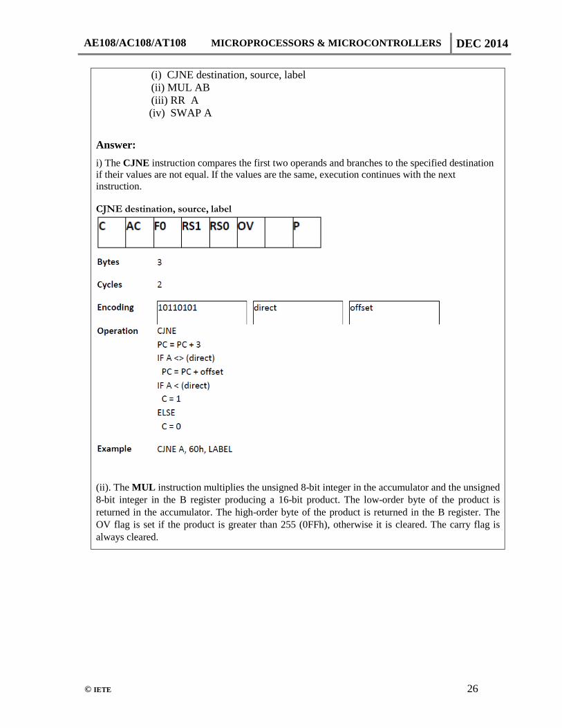
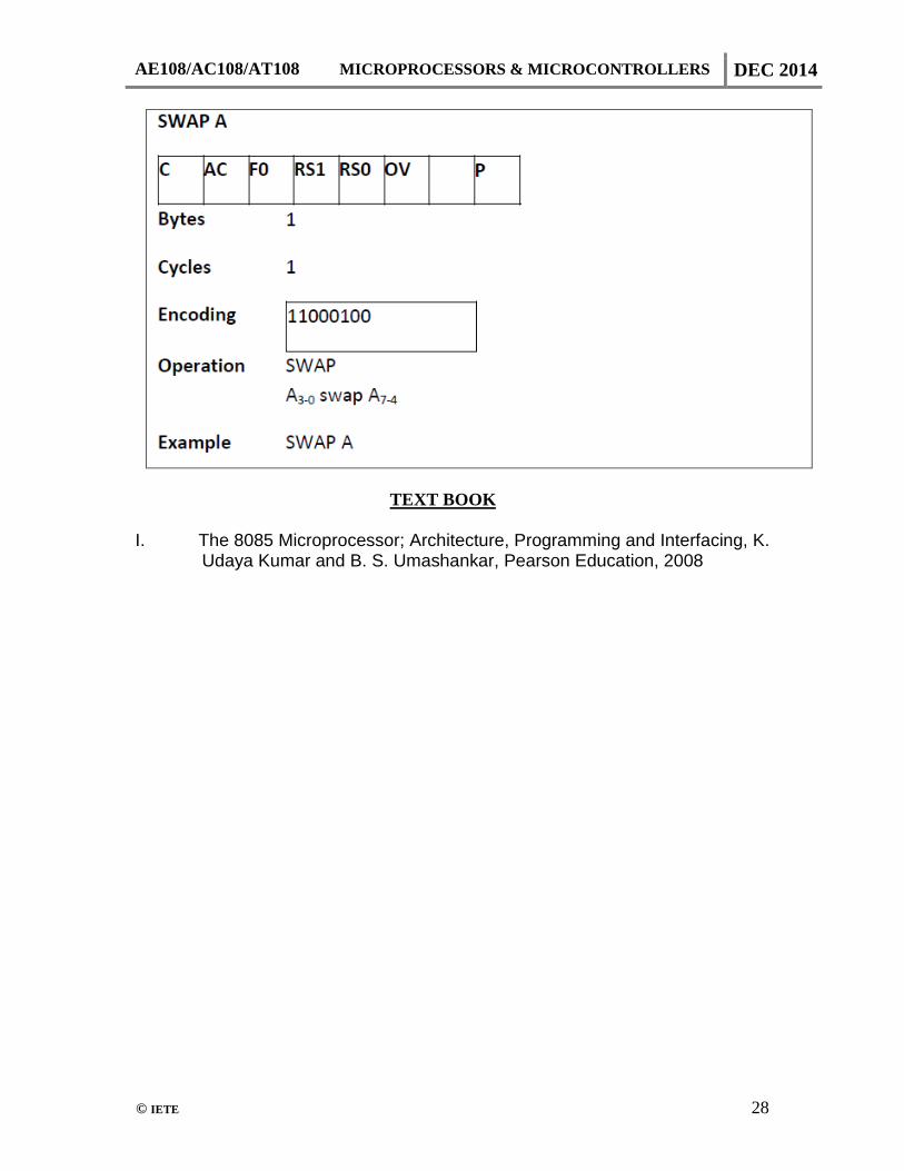
(i) CJNE destination, source, label (ii) MUL AB
(iii) RR A (iv) SWAP A
Answer: i) The CJNE instruction compares the first two operands and branches to the specified destination if their values are not equal. If the values are the same, execution continues with the next instruction. CJNE destination, source, label
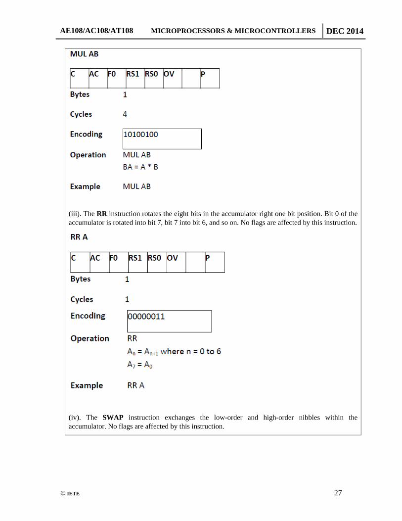
(ii). The MUL instruction multiplies the unsigned 8-bit integer in the accumulator and the unsigned 8-bit integer in the B register producing a 16-bit product. The low-order byte of the product is returned in the accumulator. The high-order byte of the product is returned in the B register. The OV flag is set if the product is greater than 255 (0FFh), otherwise it is cleared. The carry flag is always cleared.
AE108/AC108/AT108 MICROPROCESSORS & MICROCONTROLLERS DEC 2014
© IETE 27
(iii). The RR instruction rotates the eight bits in the accumulator right one bit position. Bit 0 of the accumulator is rotated into bit 7, bit 7 into bit 6, and so on. No flags are affected by this instruction.
(iv). The SWAP instruction exchanges the low-order and high-order nibbles within the accumulator. No flags are affected by this instruction.
AE108/AC108/AT108 MICROPROCESSORS & MICROCONTROLLERS DEC 2014
© IETE 28
TEXT BOOK I. The 8085 Microprocessor; Architecture, Programming and Interfacing, K.
Udaya Kumar and B. S. Umashankar, Pearson Education, 2008


![Q.1(i) State the features of 80386 microprocessor [4] Ans ...diploma.vidyalankar.org/prelim-papers/TY/cmpn/AMP_Soln.pdf · ... Differentiate between .COM and ... Advantages of separate](https://img.pdfslide.net/doc/110x75/5b59cdf27f8b9ad0048d6578/q1i-state-the-features-of-80386-microprocessor-4-ans-differentiate.jpg)