Embed Size (px)
Citation preview
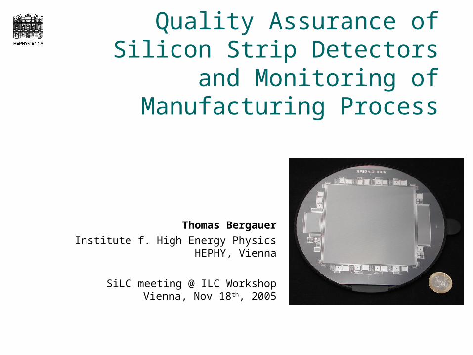
Quality Assurance of Silicon Strip Detectors and Monitoring of
Manufacturing Process
Thomas BergauerInstitute f. High Energy Physics
HEPHY, Vienna
SiLC meeting @ ILC Workshop Vienna, Nov 18th, 2005
Thomas Bergauer, HEPHY Vienna 2
Outline of Talk
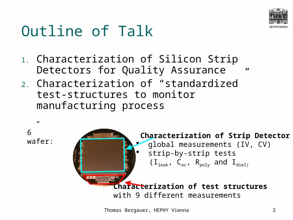
1. Characterization of Silicon Strip Detectors for Quality Assurance
2. Characterization of “standardized” test-structures to monitor manufacturing process
Characterization of Strip Detector global measurements (IV, CV) strip-by-strip tests (Ileak, Cac, Rpoly and Idiel)
Characterization of test structures with 9 different measurements
6” wafer:

1. Quality Assurance of Silicon Strip Detectors
Thomas Bergauer, HEPHY Vienna 4
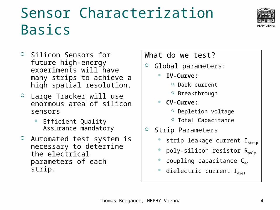
Sensor Characterization Basics
Silicon Sensors for future high-energy experiments will have many strips to achieve a high spatial resolution.
Large Tracker will use enormous area of silicon sensors
Efficient Quality Assurance mandatory
Automated test system is necessary to determine the electrical parameters of each strip.
What do we test? Global parameters:
IV-Curve: Dark current Breakthrough
CV-Curve: Depletion voltage Total Capacitance
Strip Parameters strip leakage current
Istrip
poly-silicon resistor Rpoly
coupling capacitance Cac
dielectric current Idiel
Thomas Bergauer, HEPHY Vienna 5
AC-coupled Silicon Strip Detector
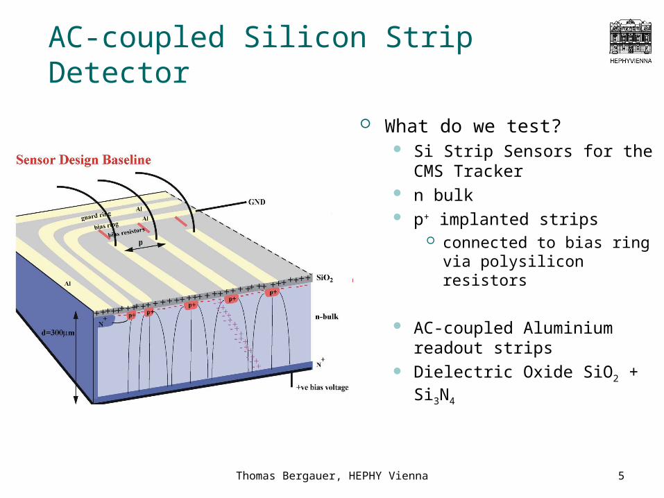
What do we test? Si Strip Sensors for the
CMS Tracker n bulk p+ implanted strips
connected to bias ring via polysilicon resistors
AC-coupled Aluminium readout strips
Dielectric Oxide SiO2 + Si3N4
Thomas Bergauer, HEPHY Vienna 6
AC-coupled Silicon Strip Detector
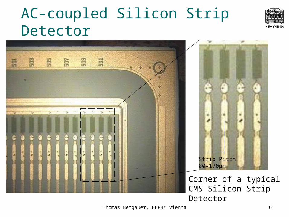
Corner of a typical CMS Silicon Strip Detector
Strip Pitch80-170μm
Thomas Bergauer, HEPHY Vienna 7
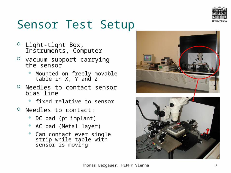
Sensor Test Setup
Light-tight Box, Instruments, Computer
vacuum support carrying the sensor
Mounted on freely movable table in X, Y and Z
Needles to contact sensor bias line
fixed relative to sensor Needles to contact:
DC pad (p+ implant) AC pad (Metal layer) Can contact ever single
strip while table with sensor is moving

Thomas Bergauer, HEPHY Vienna 8
Sensor Test Schematics
Instruments (HV source, Amp-Meter, LCR-Meter,…) on the left are connected via a cross-point switching matrix to the needles which contact the sensor to perform different measurements

Thomas Bergauer, HEPHY Vienna 9
Example Measurements: CV, IV
Combined voltage ramp up to 500-800V Dark current (blue) and
total capacitance (red, plotted 1/C2) is recorded.
Depletion voltage is extracted
Thomas Bergauer, HEPHY Vienna 10
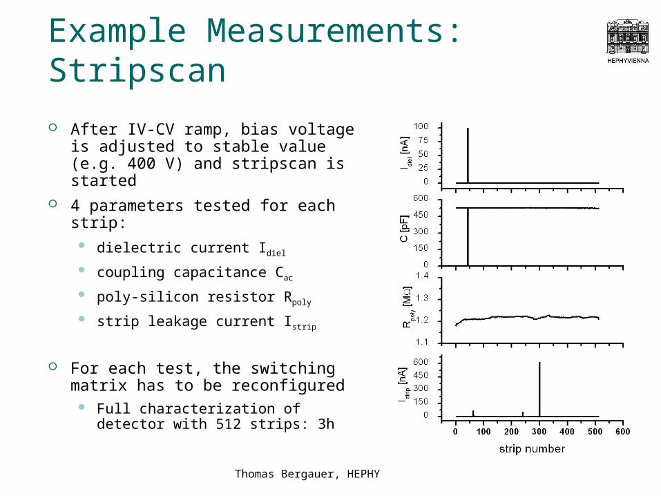
Example Measurements: Stripscan
After IV-CV ramp, bias voltage is adjusted to stable value (e.g. 400 V) and stripscan is started
4 parameters tested for each strip:
dielectric current Idiel
coupling capacitance Cac
poly-silicon resistor Rpoly
strip leakage current Istrip
For each test, the switching matrix has to be reconfigured
Full characterization of detector with 512 strips: 3h

Thomas Bergauer, HEPHY Vienna 11
Example Results: Depletion Voltage, Dark current (Sensors for CMS)
Depletion Voltage Dark current @ 450V

Thomas Bergauer, HEPHY Vienna 12
Results: Stripscan
Total number of bad strips
Total = sum of Istrip , Rpoly, Cac, Idiel )
Bad = outside specified cuts
CMS requires less than 1% of strips are outside cuts for at least one of the strip parameters
Average bad strips per sensor:
0,37

2. Monitoring of Manufacturing Process
“PQC”…. Process Quality Control

Thomas Bergauer, HEPHY Vienna 14
Motivation and Assumptions
Full Characterization of Strip Detector has some disadvantages
takes a lot of time (if every strip is checked) Only sample tests possible (assumption that production
batch behave similar) Some interesting parameters are not accessible on
standard detector or would require destructive tests
Remedy: Doing similar measurements on standardized test-structures
Assumption: Test structures behave identical to main sensor, since produced on the same wafer
Measure many parameter, each on a dedicated test structure
Destructive Tests possible Fast measurement possible
Thomas Bergauer, HEPHY Vienna 15
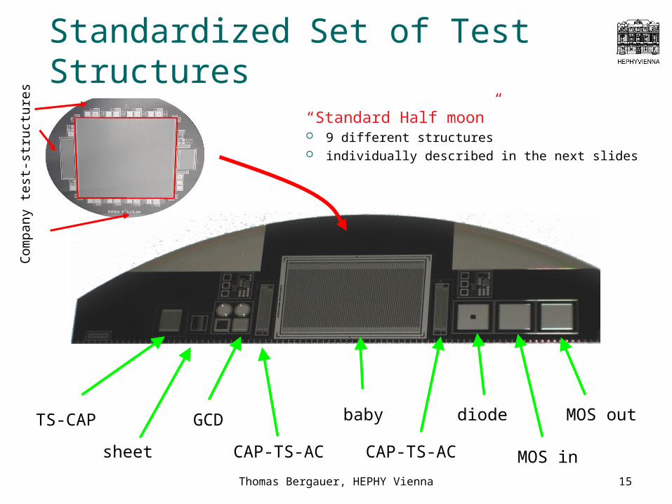
TS-CAP
sheet
GCD
CAP-TS-AC CAP-TS-AC
baby diode
MOS in
MOS out
Standardized Set of Test Structures
Company test-structures
“Standard Half moon” 9 different structures individually described in the next slides

Thomas Bergauer, HEPHY Vienna 16
Test Structures
TS-CAP: Coupling capacitance CAC to
determine oxide thickness IV-Curve: breakthrough
voltage of oxide
Sheet: Aluminium resistivity p+-impant resistivity Polysilicon resistivity
GCD: Gate Controlled Diode IV-Curve to determine surface
current Isurface
Characterize Si-SiO2 interface
CAP-TS-AC: Inter-strip capacitance Cint
Baby-Sensor: IV-Curve for dark current Breakthrough
CAP-TS-DC: Inter-strip Resistance Rint
Diode: CV-Curve to determine depletion
voltage Vdepletion Calculate resistivity of
silicon bulk
MOS: CV-Curve to extract flatband
voltage Vflatband to characterize fixed oxide charges
(details on next slide)

Thomas Bergauer, HEPHY Vienna 17
MOS Metal Oxide Semiconductor Oxide composition represents configuration of
Thick dielectric in inter-strip region Thin dielectric underneath strips (right)
Extraction of flatband voltage Vfb
Seen by sharp decrease of Capacitance (between accumulation and inversion)
to determine fixed positive charges in Oxide
Limit defined experimental after test beam

Thomas Bergauer, HEPHY Vienna 18
Setup Description Probe-card with 40 needles
contacts all pads of test structures in parallel
Half moon fixed by vacuum Micropositioner used for
Alignment In light-tight box with
humidity and temperature control
Instruments Source Measurement Unit (SMU) Voltage Source LCR-Meter (Capacitance)
Heart of the system: Crosspoint switching box
Used to switch instruments to different needles
PC with Labview used to control instruments and switching system
GPIB Bus for communication

Thomas Bergauer, HEPHY Vienna 19
PQC Setup

Thomas Bergauer, HEPHY Vienna 20
Software
Self-developed LabVIEW program Fully automatic measurement procedure (~30 minutes)
Except alignment of Half moon and placement of probecard Automatic extraction of parameters
Before run:
After run:
Yellow Fields: Limits and cuts for qualification
Blue Fields: Obtained resultsextracted from graphby linear fits (red/green lines)
Thomas Bergauer, HEPHY Vienna 21
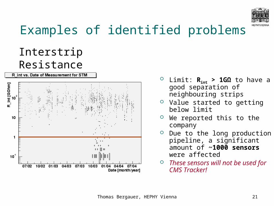
Examples of identified problems
Limit: Rint > 1GΩ to have a good separation of neighbouring strips
Value started to getting below limit
We reported this to the company
Due to the long production pipeline, a significant amount of ~1000 sensors were affected
These sensors will not be used for CMS Tracker!
Interstrip Resistance
Thomas Bergauer, HEPHY Vienna 22
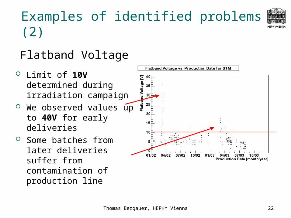
Examples of identified problems (2)
Limit of 10V determined during irradiation campaign
We observed values up to 40V for early deliveries
Some batches from later deliveries suffer from contamination of production line
Flatband Voltage
Thomas Bergauer, HEPHY Vienna 23
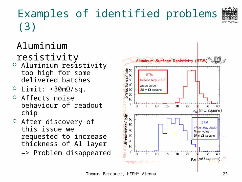
Examples of identified problems (3)
Aluminium resistivity too high for some delivered batches
Limit: <30mΩ/sq. Affects noise
behaviour of readout chip
After discovery of this issue we requested to increase thickness of Al layer=> Problem disappeared
Aluminium resistivity

Thomas Bergauer, HEPHY Vienna 24
Summary Future experiments with a large tracker will require a
huge number of silicon strip sensors. Compare with CMS Silicon Strip Tracker: 206 m2 is equal to
24.244 pieces of sensors and 9.316.352 channels
Its fabrication will last many months (years) and a stable production during the whole production time is mandatory.
Strip-by-strip test of detectors is necessary but not sufficient
Slow, reduced set of parameters to test
Measurements on dedicated test-structures is a powerful possibility to monitor the fabrication process
During a long production time Also on parameters which are not accessible on the main sensor
(e.g. MOS, GCD,... ) Destructive tests possible Fast measurement allows high throughput

Thomas Bergauer, HEPHY Vienna 25
Outlook and Future Plans
We have to optimize our test structures We learned during the CMS QA that some things can be improved:
Smaller structures Better design of some structures (e.g. diode, sheet)
We want to offer this standardized set of test structures to all interested groups in the future To put it on unused space of their wafer design
Thanks.

The End.

Backup Slides

Thomas Bergauer, HEPHY Vienna 28
TS CAP
Array of 26 AC-coupled strips
Test of Coupling Capacitance Oxide Thickness can calculated
Test of dielectric breakdown Destructive !

Thomas Bergauer, HEPHY Vienna 29
Sheet
Combination of Three polysilicon resistors Three Aluminium Strips (10, 20,
50 um thickness) Three p+ Strips (10, 20, 50 um
thickness) Used to determine resistivity of
implant, Aluminium and polysilicon
These Parameters have influence on noise behavior of readout chip
Thomas Bergauer, HEPHY Vienna 30
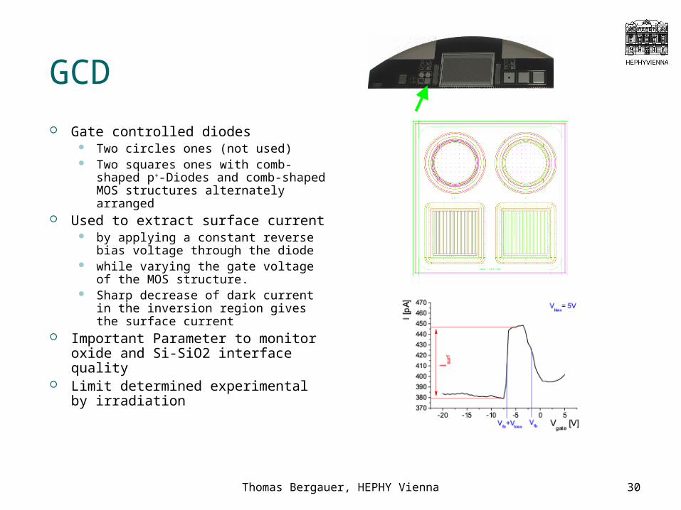
GCD
Gate controlled diodes Two circles ones (not used) Two squares ones with comb-
shaped p+-Diodes and comb-shaped MOS structures alternately arranged
Used to extract surface current
by applying a constant reverse bias voltage through the diode
while varying the gate voltage of the MOS structure.
Sharp decrease of dark current in the inversion region gives the surface current
Important Parameter to monitor oxide and Si-SiO2 interface quality
Limit determined experimental by irradiation
Thomas Bergauer, HEPHY Vienna 31
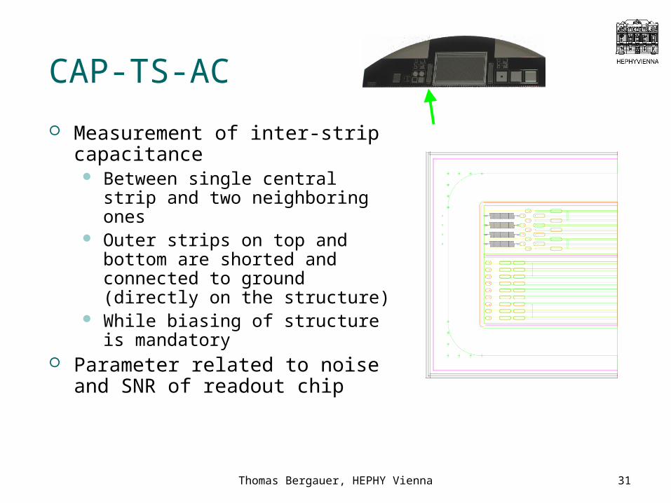
CAP-TS-AC
Measurement of inter-strip capacitance Between single central strip and two neighboring ones
Outer strips on top and bottom are shorted and connected to ground (directly on the structure)
While biasing of structure is mandatory
Parameter related to noise and SNR of readout chip

Thomas Bergauer, HEPHY Vienna 32
Baby Sensor
Structure with 192 AC-coupled strips
Identical to main detector Used to measure IV-curve up to
700 V Breakthrough voltage is
determined
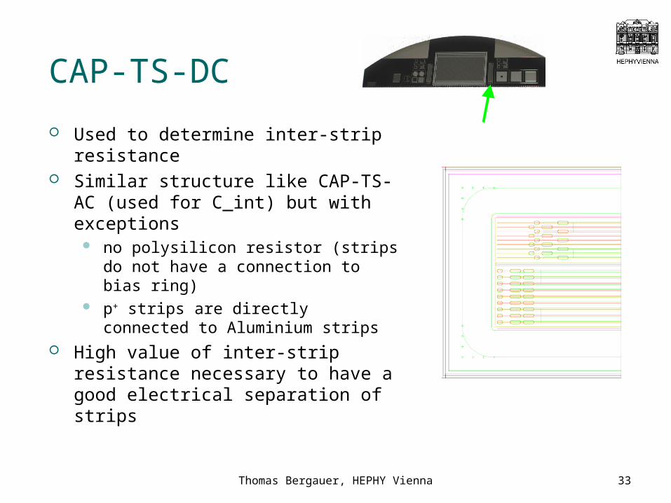
Thomas Bergauer, HEPHY Vienna 33
CAP-TS-DC
Used to determine inter-strip resistance
Similar structure like CAP-TS-AC (used for C_int) but with exceptions
no polysilicon resistor (strips do not have a connection to bias ring)
p+ strips are directly connected to Aluminium strips
High value of inter-strip resistance necessary to have a good electrical separation of strips

Thomas Bergauer, HEPHY Vienna 34
Diode
Simple square diode Voltage scan is used to
measure Capacitance and to extract total bulk thickness
Bulk resistivity
Cdepl 0rA
d
d2nominal
20reVdepl