Embed Size (px)
Citation preview
1
SiLC Silicon Sensors: Status of different activities
Thomas Bergauer
for the SiLC Collaboration
April 25th, 2007Outline:• SiLC “Sensor Baseline”• DESY TPC• Synergies with SLHC• Status of companies
2
Linear Collider Constraints
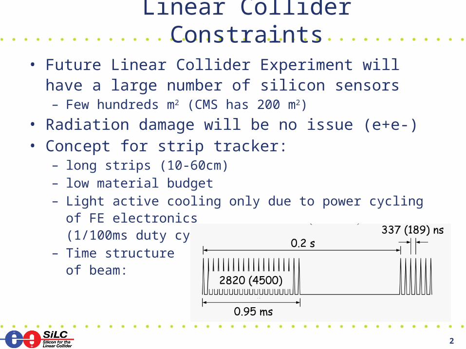
• Future Linear Collider Experiment will have a large number of silicon sensors– Few hundreds m2 (CMS has 200 m2)
• Radiation damage will be no issue (e+e-)• Concept for strip tracker:
– long strips (10-60cm)– low material budget– Light active cooling only due to power cycling of FE electronics
(1/100ms duty cycle)– Time structure
of beam:
3
SilC Silicon Sensor Baseline
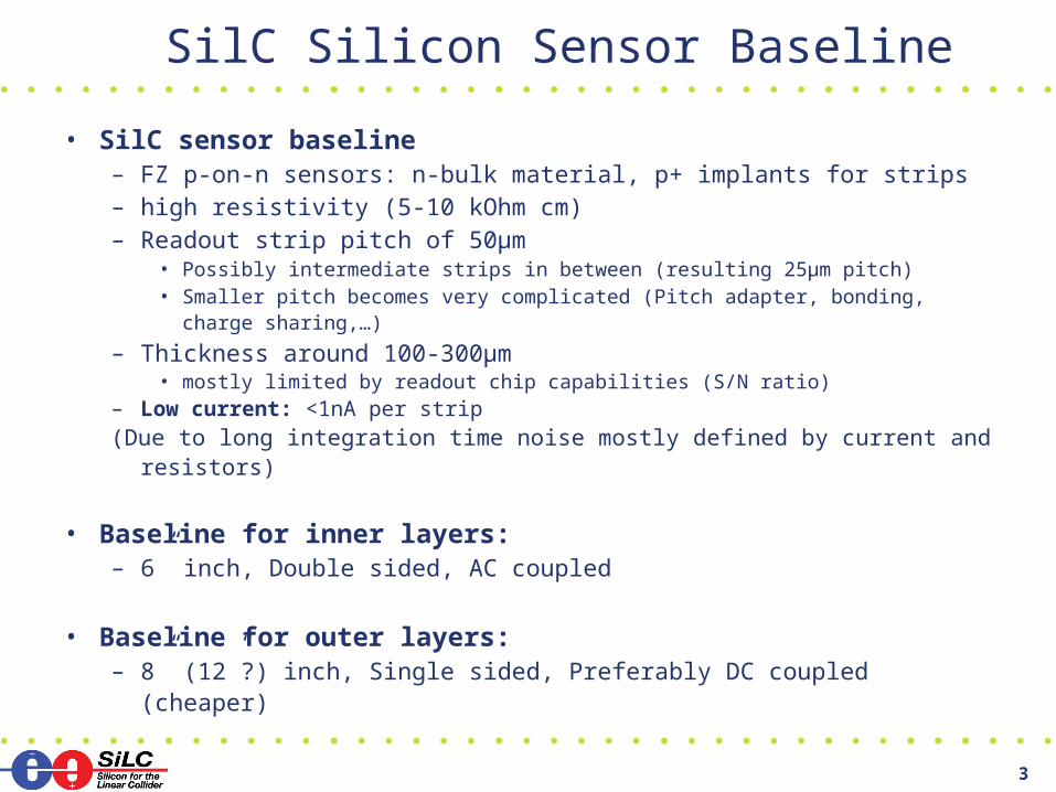
• SilC sensor baseline– FZ p-on-n sensors: n-bulk material, p+ implants for strips– high resistivity (5-10 kOhm cm)– Readout strip pitch of 50µm
• Possibly intermediate strips in between (resulting 25µm pitch)• Smaller pitch becomes very complicated (Pitch adapter, bonding, charge sharing,
…)
– Thickness around 100-300µm• mostly limited by readout chip capabilities (S/N ratio)
– Low current: <1nA per strip(Due to long integration time noise mostly defined by current and resistors)
• Baseline for inner layers:– 6” inch, Double sided, AC coupled
• Baseline for outer layers:– 8” (12”?) inch, Single sided, Preferably DC coupled (cheaper)
4
Sensor Baseline Details
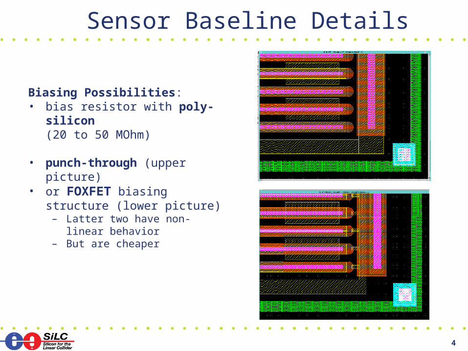
Biasing Possibilities:• bias resistor with poly-silicon
(20 to 50 MOhm)
• punch-through (upper picture)• or FOXFET biasing structure
(lower picture)– Latter two have non-linear
behavior– But are cheaper
5
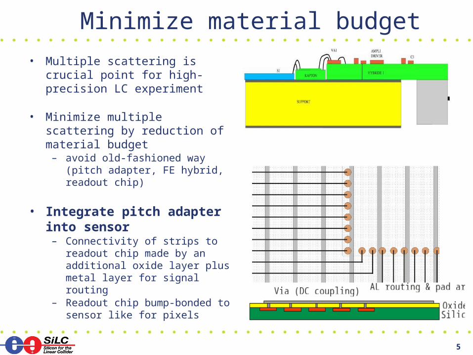
Minimize material budget
• Multiple scattering is crucial point for high-precision LC experiment
• Minimize multiple scattering by reduction of material budget
– avoid old-fashioned way (pitch adapter, FE hybrid, readout chip)
• Integrate pitch adapter into sensor
– Connectivity of strips to readout chip made by an additional oxide layer plus metal layer for signal routing
– Readout chip bump-bonded to sensor like for pixels
6
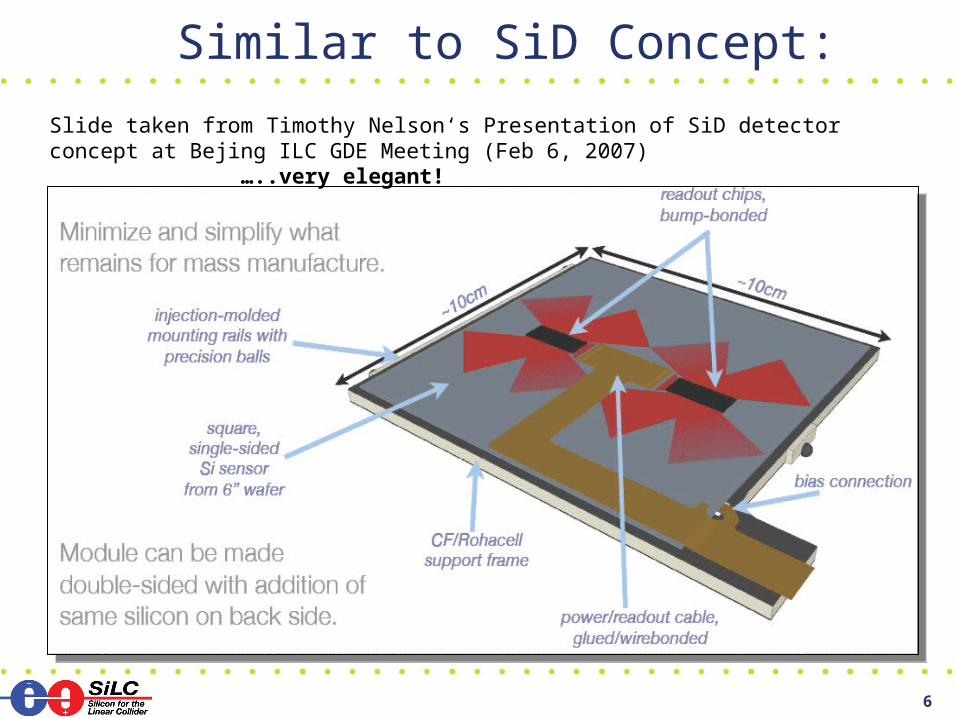
Similar to SiD Concept:
Slide taken from Timothy Nelson‘s Presentation of SiD detector concept at Bejing ILC GDE Meeting (Feb 6, 2007) …..very elegant!
7
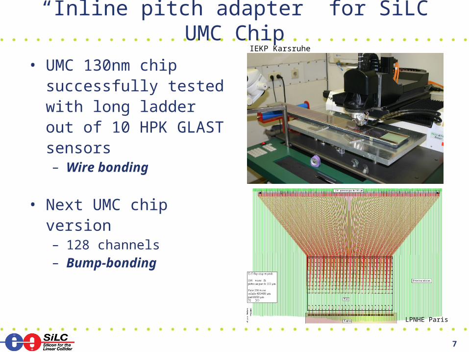
“Inline pitch adapter” for SiLC UMC Chip
• UMC 130nm chip successfully tested with long ladder out of 10 HPK GLAST sensors – Wire bonding
• Next UMC chip version – 128 channels– Bump-bonding
LPNHE Paris
IEKP Karsruhe
8
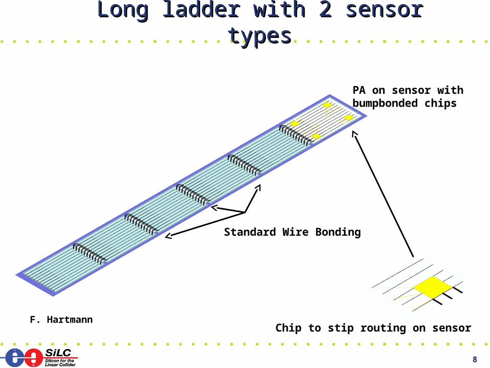
Long ladder with 2 sensor typesLong ladder with 2 sensor types
F. Hartmann
Standard Wire Bonding
PA on sensor withbumpbonded chips
Chip to stip routing on sensor
9
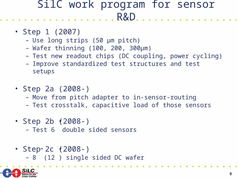
SilC work program for sensor R&D
• Step 1 (2007)– Use long strips (50 µm pitch)– Wafer thinning (100, 200, 300µm)– Test new readout chips (DC coupling, power cycling)– Improve standardized test structures and test setups
• Step 2a (2008-)– Move from pitch adapter to in-sensor-routing– Test crosstalk, capacitive load of those sensors
• Step 2b (2008-)– Test 6” double sided sensors
• Step 2c (2008-)– 8” (12”) single sided DC wafer
10
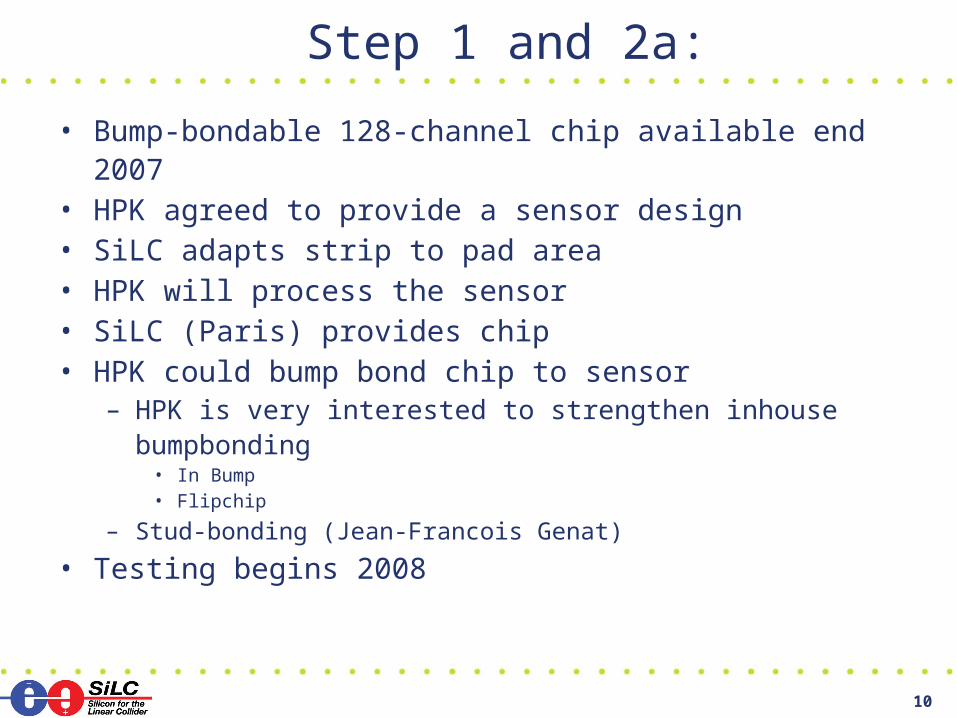
Step 1 and 2a:
• Bump-bondable 128-channel chip available end 2007• HPK agreed to provide a sensor design• SiLC adapts strip to pad area• HPK will process the sensor• SiLC (Paris) provides chip• HPK could bump bond chip to sensor
– HPK is very interested to strengthen inhouse bumpbonding• In Bump• Flipchip
– Stud-bonding (Jean-Francois Genat)
• Testing begins 2008
11
DESY TPC
12
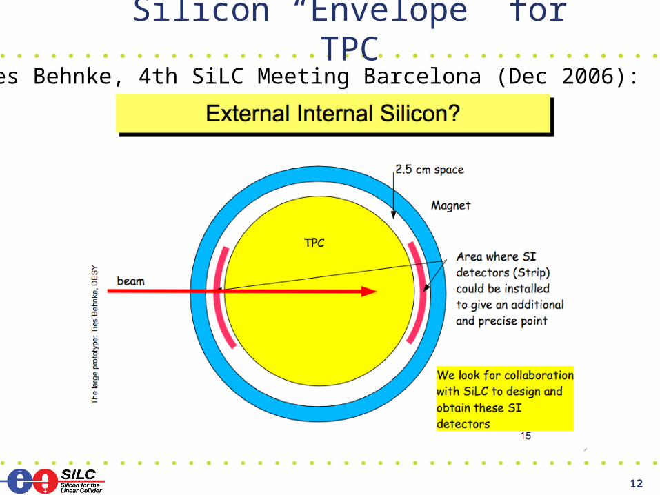
Silicon “Envelope” for TPCTies Behnke, 4th SiLC Meeting Barcelona (Dec 2006):
13
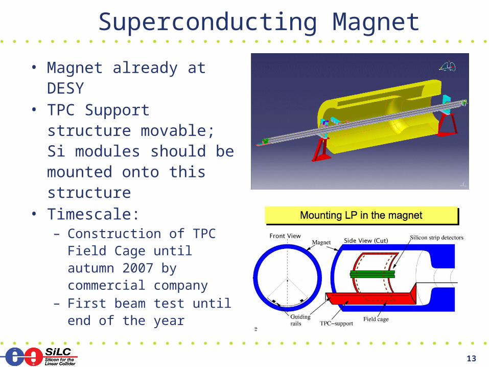
Superconducting Magnet
• Magnet already at DESY• TPC Support structure
movable; Si modules should be mounted onto this structure
• Timescale:– Construction of TPC Field
Cage until autumn 2007 by commercial company
– First beam test until end of the year
14
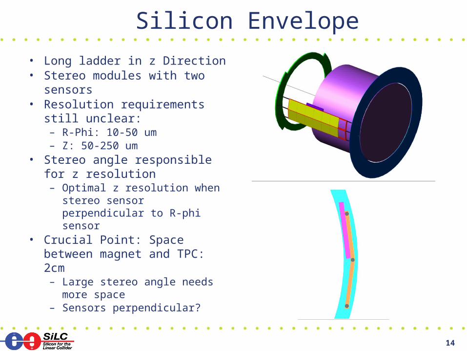
Silicon Envelope
• Long ladder in z Direction• Stereo modules with two
sensors• Resolution requirements still
unclear:– R-Phi: 10-50 um– Z: 50-250 um
• Stereo angle responsible for z resolution– Optimal z resolution when
stereo sensor perpendicular to R-phi sensor
• Crucial Point: Space between magnet and TPC: 2cm– Large stereo angle needs
more space– Sensors perpendicular?
15
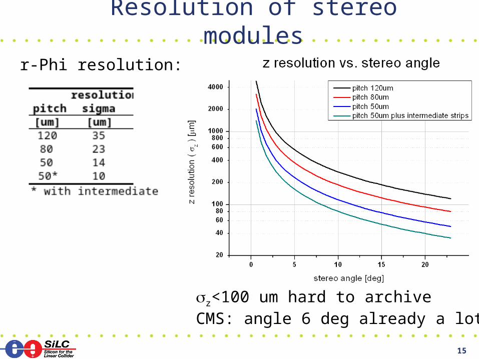
Resolution of stereo modules
r-Phi resolution:
z<100 um hard to archiveCMS: angle 6 deg already a lot!
16
Next Steps
• Sensor procurement from HPK– Details about HPK offer later– Sensors tests @ Vienna, Karlsruhe
• Find material for module frame/support– Rohacell, Silicon foam– Carbon Fiber, Graphite
• Define module/ladder geometry– Maximum number of daisy-chained sensors?
• Depends on S/N ratio of chip (Jean-Francois?)
– Layout of FE hybrid and Chip pitch needed (Jean-Francois?)
• Everybody who is interested is welcome to join the phone/video meeting. Just send me a mail and I will take you on the list.
• Plan to have a tour to the TPC magnet during LCWS07 in Hamburg (end of May)
17
Synergies with (S)LHC
LHC Upgrade project is called “super” LHC
18
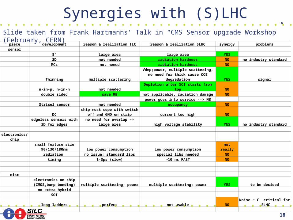
Synergies with (S)LHC
piece development reason & realization ILC reason & realization SLHC synergy problemssensor
8" large area large area YES 3D not needed radiation hardness NO no industry standard MCz not neeed radiation hardness NO
Thinning multiple scatteringVdep;power, multiple scattering, no need
for thick cause CCE degradation YES signal n-in-p, n-in-n not needed Depletion after SCI starts from top NO double sided save MB not applicable, radiation damage NO power goes into service --> MB Strixel sensor not needed occupancy NO
DCchip must cope with switch off
and GND on strip current too high NO
edgeless sensors with 3D
for edges no need for overlap => large area high voltage stability YES no industry standard
electronics/chip
small feature size
90/130/180nm low power consumption low power consumption not really radiation no issue; standard libs special libs needed NO timing 1-3µs (slow) ~10 ns FAST NO
misc
electronics on chip
(CMOS,bump bonding) multiple scattering; power multiple scattering; power YES to be decided no extra hybrid SOI long ladders perfect not usable NO Noise ~ C critical for SLHC
Slide taken from Frank Hartmanns’ Talk in “CMS Sensor upgrade Workshop” (February, CERN)
19
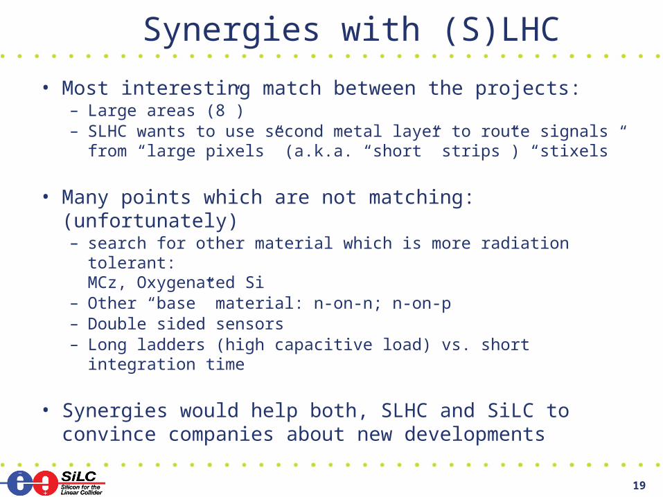
Synergies with (S)LHC
• Most interesting match between the projects:– Large areas (8”)– SLHC wants to use second metal layer to route signals from
“large pixels” (a.k.a. “short” strips”) “stixels”
• Many points which are not matching: (unfortunately)– search for other material which is more radiation tolerant:
MCz, Oxygenated Si– Other “base” material: n-on-n; n-on-p– Double sided sensors – Long ladders (high capacitive load) vs. short integration time
• Synergies would help both, SLHC and SiLC to convince companies about new developments
20
Status of the companies
21
HPK
• During Vienna Conference “VCI” (Feb 2007): Meeting with HPK’s European Sales representant and Japanese engineer.
• We had several questions which have been answered by them (later by e-mail):– Double sided processing (6”)? Not possible– Cost difference AC-DC coupling: AC is 40-50% more expensive– Cost difference biasing (DC=100): PT: 115; FOXFET : 120; Poly-Si : 130 – Minimal sensor thickness? 200 micron (possible in 1 year from now)– Maximum dielectric layer? 1m with SiO2, maybe Polyimide in the future– Trace metallization: only Al with 0.9 m thickness and minimum width of 3
to 4 m; no other material for the time being (we asked for Copper)– Larger Sensors: 8-12” production possible via sub-contractor, but much
more expensive; limited prototyping– bump bonding: Indium bump-bonding being developed within 1 year, 20 m
pitch
• We asked HPK for an offer for 30 pcs single sided detectors with 50um pitch during this meeting.
22
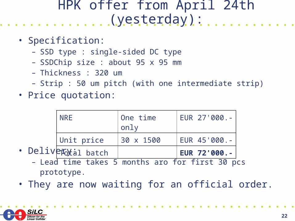
HPK offer from April 24th (yesterday):
• Specification:– SSD type : single-sided DC type – SSDChip size : about 95 x 95 mm– Thickness : 320 um– Strip : 50 um pitch (with one intermediate strip)
• Price quotation:
• Delivery:– Lead time takes 5 months aro for first 30 pcs prototype.
• They are now waiting for an official order.
NRE One time only
EUR 27'000.-
Unit price 30 x 1500 EUR 45'000.-
Total batch EUR 72'000.-
23
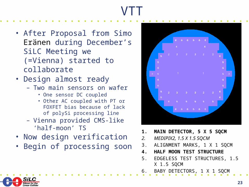
VTT
• After Proposal from Simo Eränen during December’s SiLC Meeting we (=Vienna) started to collaborate
• Design almost ready– Two main sensors on wafer
• One sensor DC coupled• Other AC coupled with PT or
FOXFET bias because of lack of polySi processing line
– Vienna provided CMS-like ‘half-moon’ TS
• Now design verification• Begin of processing soon
1. MAIN DETECTOR, 5 X 5 SQCM2. MEDIPIX2, 1.5 X 1.5 SQCM3. ALIGNMENT MARKS, 1 X 1 SQCM4. HALF MOON TEST STRUCTURE5. EDGELESS TEST STRUCTURES, 1.5
X 1.5 SQCM6. BABY DETECTORS, 1 X 1 SQCM
24
Meeting with Hwanbae Park (Korea), Jan 29th
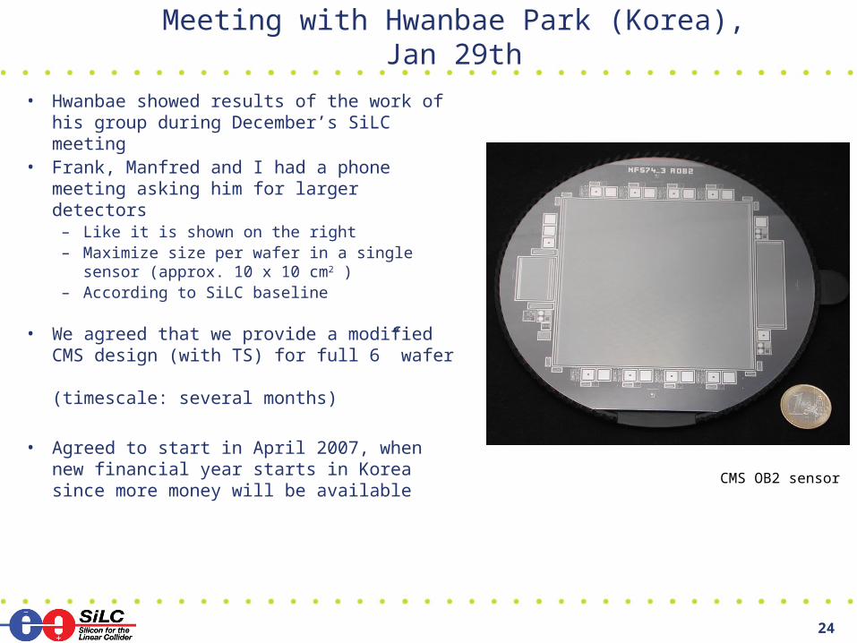
• Hwanbae showed results of the work of his group during December’s SiLC meeting
• Frank, Manfred and I had a phone meeting asking him for larger detectors
– Like it is shown on the right– Maximize size per wafer in a single sensor
(approx. 10 x 10 cm2 )– According to SiLC baseline
• We agreed that we provide a modified CMS design (with TS) for full 6” wafer (timescale: several months)
• Agreed to start in April 2007, when new financial year starts in Korea since more money will be available
CMS OB2 sensor
25
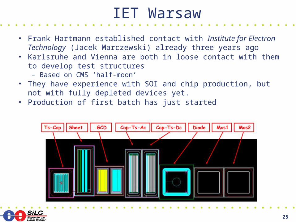
IET Warsaw
• Frank Hartmann established contact with Institute for Electron Technology (Jacek Marczewski) already three years ago
• Karlsruhe and Vienna are both in loose contact with them to develop test structures– Based on CMS ‘half-moon’
• They have experience with SOI and chip production, but not with fully depleted devices yet.
• Production of first batch has just started
26
Canberra
?(Aurore proposed to establish a contact with them)
27
ON Semiconductor
• http://www.onsemi.cz• Former “Tesla” company• Located in Czech republic• Presumably high throughput
– 4” production line running– 6” production line currently commissioned
• “first contact” can be established with help of Vaclav Vrba from Czech Academy of Sciences hopefully soon.
28
Summary
• Sensor baseline established:– FZ, p-on-n, high resistivity, 100-300um thick, 50um pitch – preferably DC coupled, otherwise biasing via PolySi, PT or FOXFET
• DESY TPC project started– Sensor procurement with HPK ongoing, but takes longer than expected– Several design decision to be made:
• Which stereo angle? (or perpendicular sensors; best resolution)• Material of Support: CF/Rohacell, CF legs like CMS, other material?• Next step: Module Construction• Layout of the FE hybrid unknown, need input from Jean-Francois
• Discussion with several companies / institutes ongoing– VTT: design almost finished– Korea: 1st design has to come from us within next weeks– IET Warsaw: TS already in production– Canberra: unknown– ON Semiconductors: 1st visit next month?
29
The End.
Backup Slides follow
30
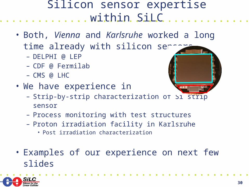
• Both, Vienna and Karlsruhe worked a long time already with silicon sensors– DELPHI @ LEP– CDF @ Fermilab– CMS @ LHC
• We have experience in – Strip-by-strip characterization of Si strip sensor– Process monitoring with test structures– Proton irradiation facility in Karlsruhe
• Post irradiation characterization
• Examples of our experience on next few slides
Silicon sensor expertise within SiLC
31
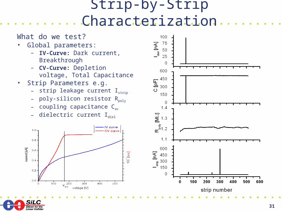
Strip-by-Strip Characterization
What do we test?• Global parameters:
– IV-Curve: Dark current, Breakthrough
– CV-Curve: Depletion voltage, Total Capacitance
• Strip Parameters e.g.– strip leakage current Istrip
– poly-silicon resistor Rpoly
– coupling capacitance Cac
– dielectric current Idiel
32
TS-CAP
sheet
GCD
CAP-TS-AC CAP-TS-AC
baby diode
MOS 1
MOS 2
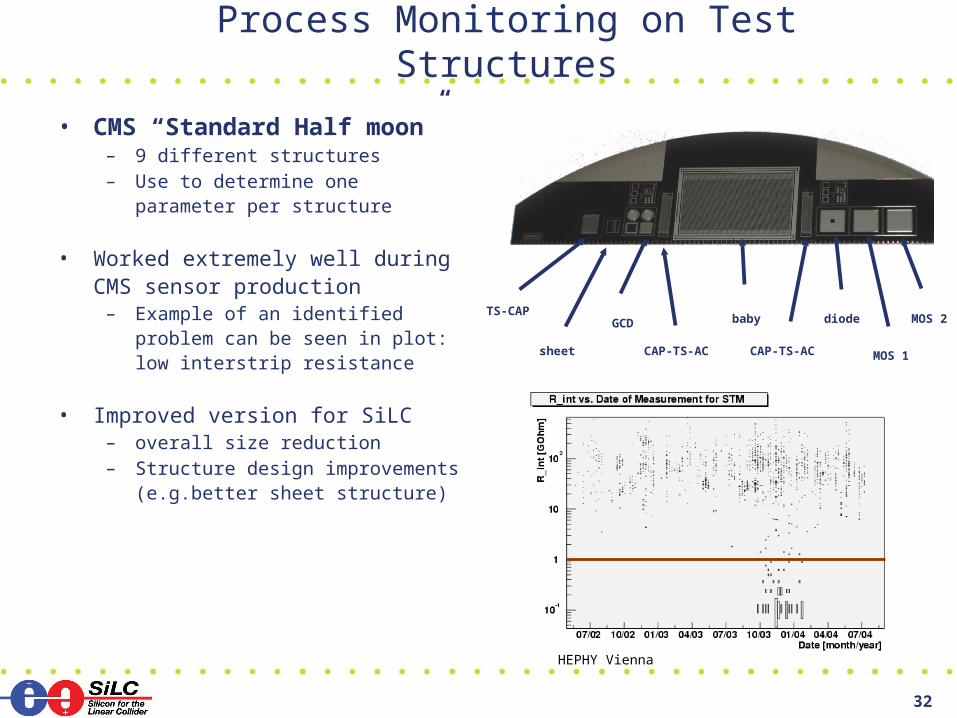
Process Monitoring on Test Structures
• CMS “Standard Half moon”– 9 different structures– Use to determine one parameter per
structure
• Worked extremely well during CMS sensor production
– Example of an identified problem can be seen in plot: low interstrip resistance
• Improved version for SiLC– overall size reduction – Structure design improvements
(e.g.better sheet structure)
HEPHY Vienna
33
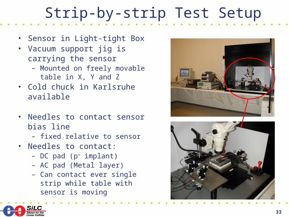
Strip-by-strip Test Setup
• Sensor in Light-tight Box• Vacuum support jig is carrying the
sensor– Mounted on freely movable table in
X, Y and Z • Cold chuck in Karlsruhe available
• Needles to contact sensor bias line – fixed relative to sensor
• Needles to contact:– DC pad (p+ implant)– AC pad (Metal layer)– Can contact ever single strip while
table with sensor is moving
34
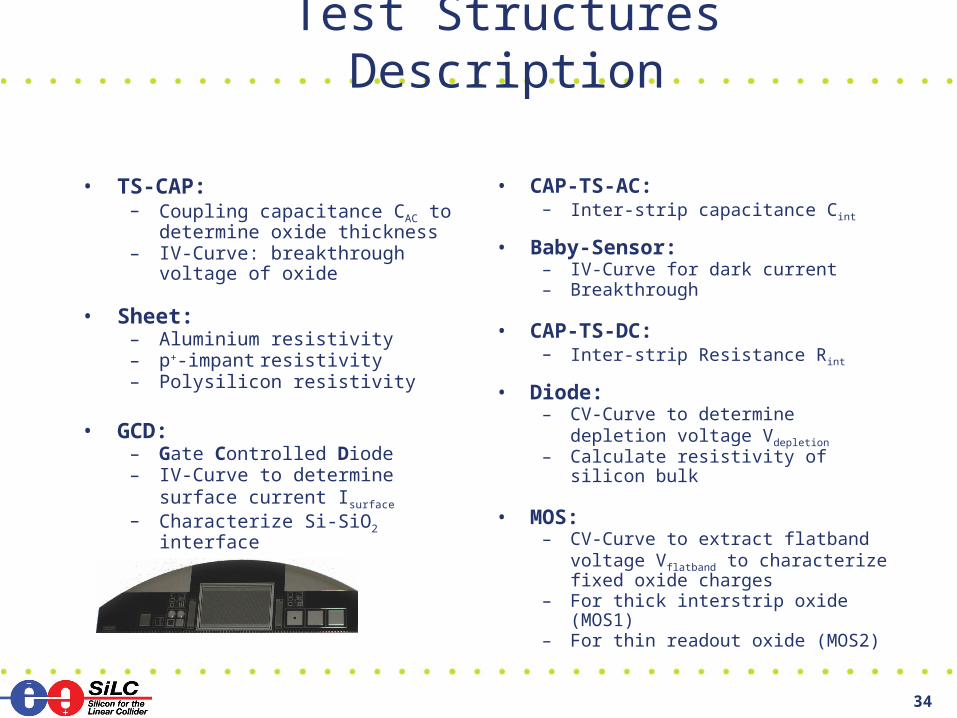
Test Structures Description
• TS-CAP:– Coupling capacitance CAC to
determine oxide thickness– IV-Curve: breakthrough voltage of
oxide
• Sheet:– Aluminium resistivity– p+-impant resistivity– Polysilicon resistivity
• GCD: – Gate Controlled Diode– IV-Curve to determine surface
current Isurface
– Characterize Si-SiO2 interface
• CAP-TS-AC: – Inter-strip capacitance Cint
• Baby-Sensor: – IV-Curve for dark current– Breakthrough
• CAP-TS-DC: – Inter-strip Resistance Rint
• Diode:– CV-Curve to determine depletion
voltage Vdepletion – Calculate resistivity of silicon bulk
• MOS: – CV-Curve to extract flatband voltage
Vflatband to characterize fixed oxide charges
– For thick interstrip oxide (MOS1)– For thin readout oxide (MOS2)
35
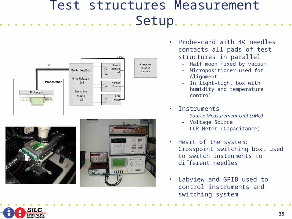
Test structures Measurement Setup
• Probe-card with 40 needles contacts all pads of test structures in parallel
– Half moon fixed by vacuum– Micropositioner used for Alignment– In light-tight box with humidity and
temperature control
• Instruments– Source Measurement Unit (SMU)– Voltage Source– LCR-Meter (Capacitance)
• Heart of the system: Crosspoint switching box, used to switch instruments to different needles
• Labview and GPIB used to control instruments and switching system
36
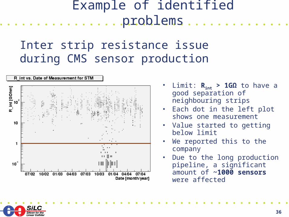
Example of identified problems
• Limit: Rint > 1GΩ to have a good separation of neighbouring strips
• Each dot in the left plot shows one measurement
• Value started to getting below limit
• We reported this to the company• Due to the long production
pipeline, a significant amount of ~1000 sensors were affected
Inter strip resistance issue during CMS sensor production
37
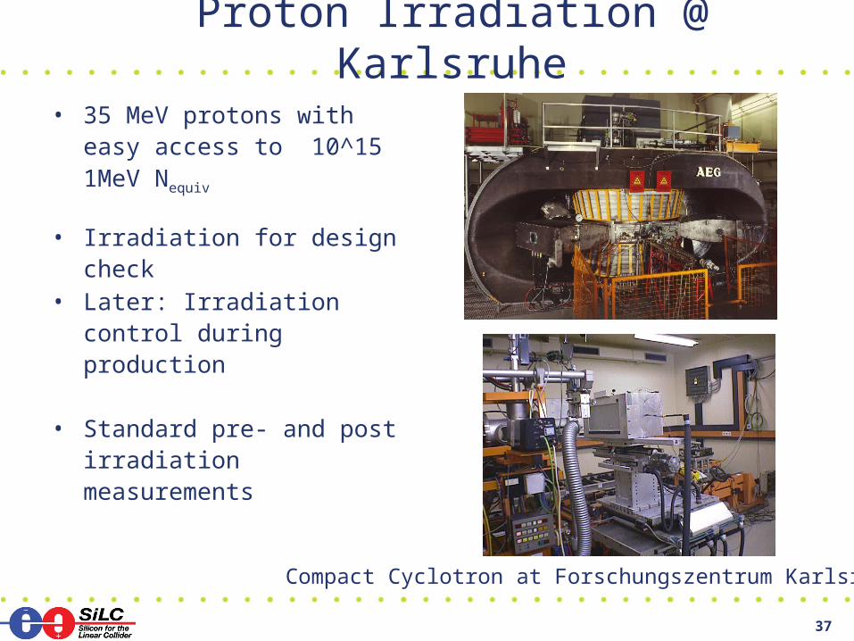
Proton Irradiation @ Karlsruhe
• 35 MeV protons with easy access to 10^15 1MeV Nequiv
• Irradiation for design check• Later: Irradiation control during
production
• Standard pre- and post irradiation measurements
Compact Cyclotron at Forschungszentrum Karlsruhe
38
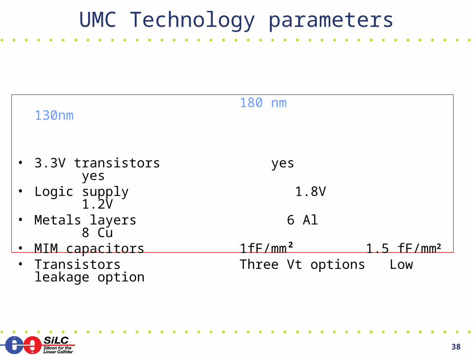
UMC Technology parameters
180 nm 130nm
• 3.3V transistors yes yes
• Logic supply 1.8V 1.2V
• Metals layers 6 Al 8 Cu
• MIM capacitors 1fF/mm² 1.5 fF/mm2
• Transistors Three Vt options Low leakage option
39
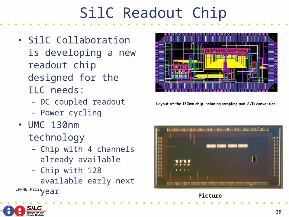
SilC Readout Chip
• SilC Collaboration is developing a new readout chip designed for the ILC needs:– DC coupled readout– Power cycling
• UMC 130nm technology– Chip with 4 channels
already available– Chip with 128 available
early next year
PictureLPNHE Paris
40
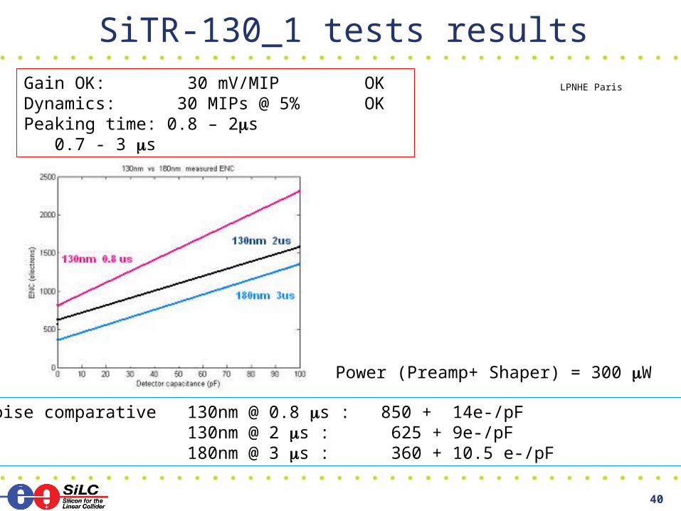
SiTR-130_1 tests resultsGain OK: 30 mV/MIP OKDynamics: 30 MIPs @ 5% OKPeaking time: 0.8 – 2s 0.7 - 3 s
Noise comparative 130nm @ 0.8 s : 850 + 14e-/pF 130nm @ 2 s : 625 + 9e-/pF 180nm @ 3 s : 360 + 10.5 e-/pF
Power (Preamp+ Shaper) = 300 W
LPNHE Paris
41
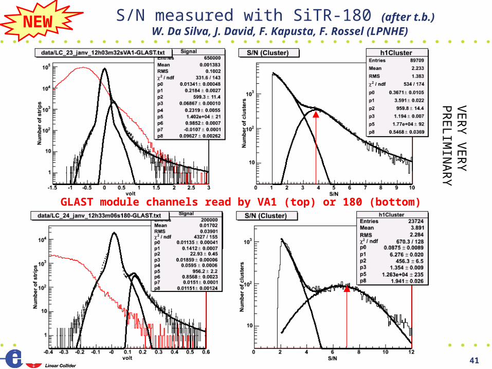
S/N measured with SiTR-180 (after t.b.) W. Da Silva, J. David, F. Kapusta, F. Rossel (LPNHE)
NEW
GLAST module channels read by VA1 (top) or 180 (bottom)
VE
RY
VE
RY
P
RE
LIMIN
AR
Y
42
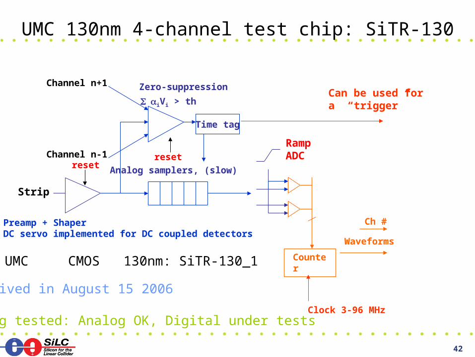
UMC 130nm 4-channel test chip: SiTR-130
UMC CMOS 130nm: SiTR-130_1 Counter
Ch #
Waveforms
RampADC
Can be used for a “trigger”
Analog samplers, (slow)
iVi > th
Zero-suppressionChannel n+1
Channel n-1
Time tag
Preamp + ShaperDC servo implemented for DC coupled detectors
Strip
reset
Clock 3-96 MHz
reset
Received in August 15 2006
Being tested: Analog OK, Digital under tests