Embed Size (px)
DESCRIPTION
Quantum Capacitance Effects In Carbon Nanotube Field-Effect Devices. L. Latessa, A. Pecchia, A. Di Carlo. University of Rome ‘Tor Vergata’. P. Lugli. Lehrstuhl fur Nanoelectronic, Munchen. Devices based on field effect (CNTFET). Planar geometry top/bottom gate (IBM). ULSI Devices - PowerPoint PPT Presentation
Citation preview

Quantum Capacitance Effects Quantum Capacitance Effects In Carbon Nanotube In Carbon Nanotube Field-Effect DevicesField-Effect Devices
L. Latessa, A. Pecchia, A. Di Carlo
P. Lugli
University of Rome ‘Tor Vergata’
Lehrstuhl fur Nanoelectronic, Munchen

Devices based on field effect (CNTFET)Devices based on field effect (CNTFET)
Planargeometry top/bottom
gate(IBM)
VerticalGeometry
coaxialgate
(Infineon)
• ULSI Devices • Quasi-1D coherent transport over long distances• Si integrable technology

gDFTBgDFTB
rErH kkk
ˆ
Green’s functions Density Functional Tight-Binding(A.Pecchia, L.Latessa, A.Di Carlo)
Atomistic simulations: Quantum treatment
rnErnErnTrnE XCHartree
0
Approximated DFT:
(2)0
,
12
repi i i
i
E n H q q E
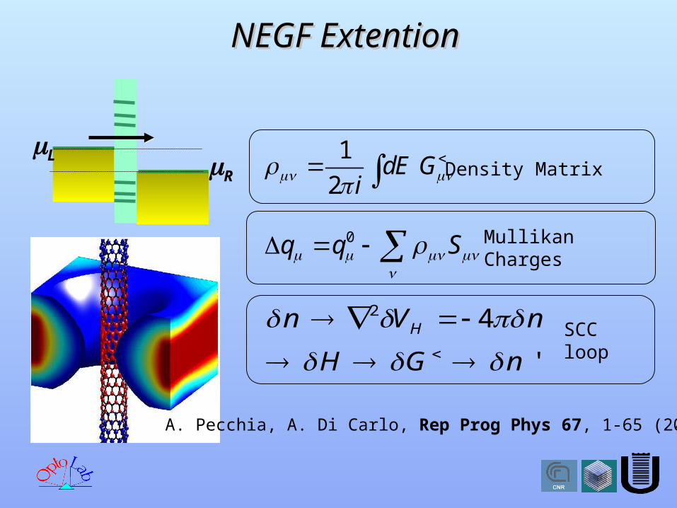
NEGF ExtentionNEGF Extention
1
2dE G
i
0q q S
Density Matrix
Mullikan Charges
2 4
'Hn V n
H G nSCCloop
L R
A. Pecchia, A. Di Carlo, Rep Prog Phys 67, 1-65 (2004)

3D Poisson Multigrid3D Poisson Multigrid
r
:0 iii CCMetal Gate rrVrC
r
Insulating dielectricand CNT
:0CCi rrVrC
2
rrVrr
4
The cylindrical gate is added as an
appropiate Dirichlet boundary condition

Coaxially gated CNTFET Coaxially gated CNTFET Working mechanisms:
• Schottky barrier modulation at the contacts
• local modulation of channel conductance
Model:
• semiconducting CNT(10,0)• neglect Schottky barrier • Charge injection from p-doped CNT contacts

CNTFET control capacitiesCNTFET control capacities
CD
CS
CG
CG
Cox
CQ
Vg
VCNT
1 1 1
G Q oxC C C
2D fC e D E
1
lE
EC
Q
1 1 1
Q E DC C C
(S.Luryi, Appl.Phys.Lett. 52, 501 (1988), sistemi 2DES)
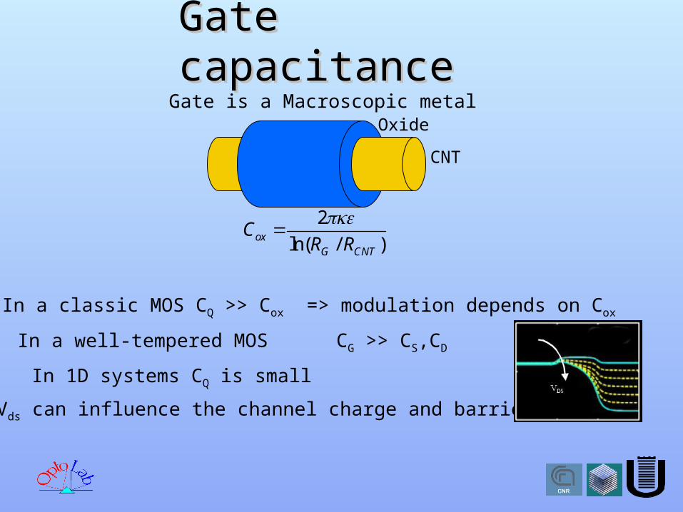
Gate capacitance Gate capacitance Gate is a Macroscopic metal
CNT
Oxide
In a well-tempered MOS CG >> CS,CD
In a classic MOS CQ >> Cox => modulation depends on Cox
Vds can influence the channel charge and barrier
In 1D systems CQ is small
2
ln( / )oxG CNT
CR R

Caratteristiche di uscita Caratteristiche di uscita IIDSDS/V/VDSDS
dEffGGTrh
eI AR
1212
2
Source
Drain
Source
Drain
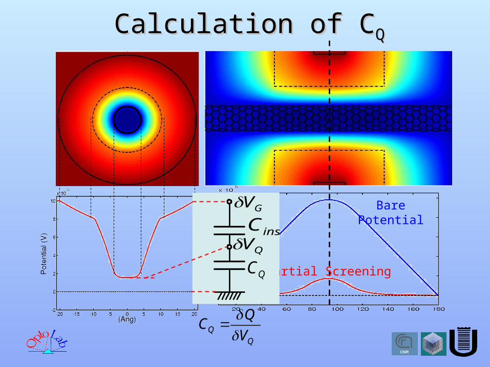
Calculation of CCalculation of CQQ
insC
Bare Potential
Partial ScreeningQC
insCGV
QV
QC
V

Over-screening in CNT Over-screening in CNT
Negative CQ Ctot > Cins The can CNT better than a
metal!
rs=5.03
rs=6.71
rs=10.06
rs=20.12
rs=6.71
rs=5.03

Negative compressibilityNegative compressibility
J.P.Eisenstein et al., Phys.Rev.Lett. 68, 647 (1992)
L.Calmels, A.Gold, Phys. Rev.B. 53, 10846 (1996)
HFAFQ
CNT
K
K
EeC
L 02
1
Experimental measurements in GaAs quantum wells
Analytic results for quasi-1D electron systems
K0 : free electrons compressibilityKHFA: Hartree-Fock exchange compress.
1 2K nn
1
QC Q

Many-body exchange effectMany-body exchange effect
Charge carrier density nC: TOTAL SCREENING CNT ~ macroscopico
High density:PARTIAL SCREENING
Dominated by DOS
Low density: OVER-SCREENINGExchange interaction preveal
Calcolo DFT
CQ= e2(EF)
2
0
XCQ F
KC e E
K

XC in XC in gDFTBgDFTB
rs=5.03
rs=6.71
rs=10.06
rs=20.12
In DFTB the XC term is treated with a Hubbard on-site energy
Substituting UH with Uee accounts only for Hartree
The capacity becomes positive again

Quantum Capacitance vs DOSQuantum Capacitance vs DOS1/DOS
KK
EeC
L
F
CNT 02
1

Over-screening and modulationOver-screening and modulation
VGS
Unconventional Trans-characteristicsPossible applications ?
VGS

ConclusionsConclusions
Comprehensive calculation of Quantum Capacity in a CNT(10,0) using NEGF
XC effects can give deviations from “classical” CQ
Negative CQ below a crytical carrier density which compares well with analytic results in quasi 1D systems
More complicated behaviour when more subbands are occupied