Embed Size (px)
Citation preview
8/8/2019 Quantum Transport :Atom to Transistor,Capacitance: Model Hamiltonian
http://slidepdf.com/reader/full/quantum-transport-atom-to-transistorcapacitance-model-hamiltonian 1/14
Quantum Transport:Quantum Transport:Atom to Transistor
Prof. Supriyo DattaECE 659Purdue University
Network for Computational Nanotechnology
03.10.2003
Lecture 23: Capacitance: Model HamiltonianRef. Chapter 7.1
8/8/2019 Quantum Transport :Atom to Transistor,Capacitance: Model Hamiltonian
http://slidepdf.com/reader/full/quantum-transport-atom-to-transistorcapacitance-model-hamiltonian 2/14
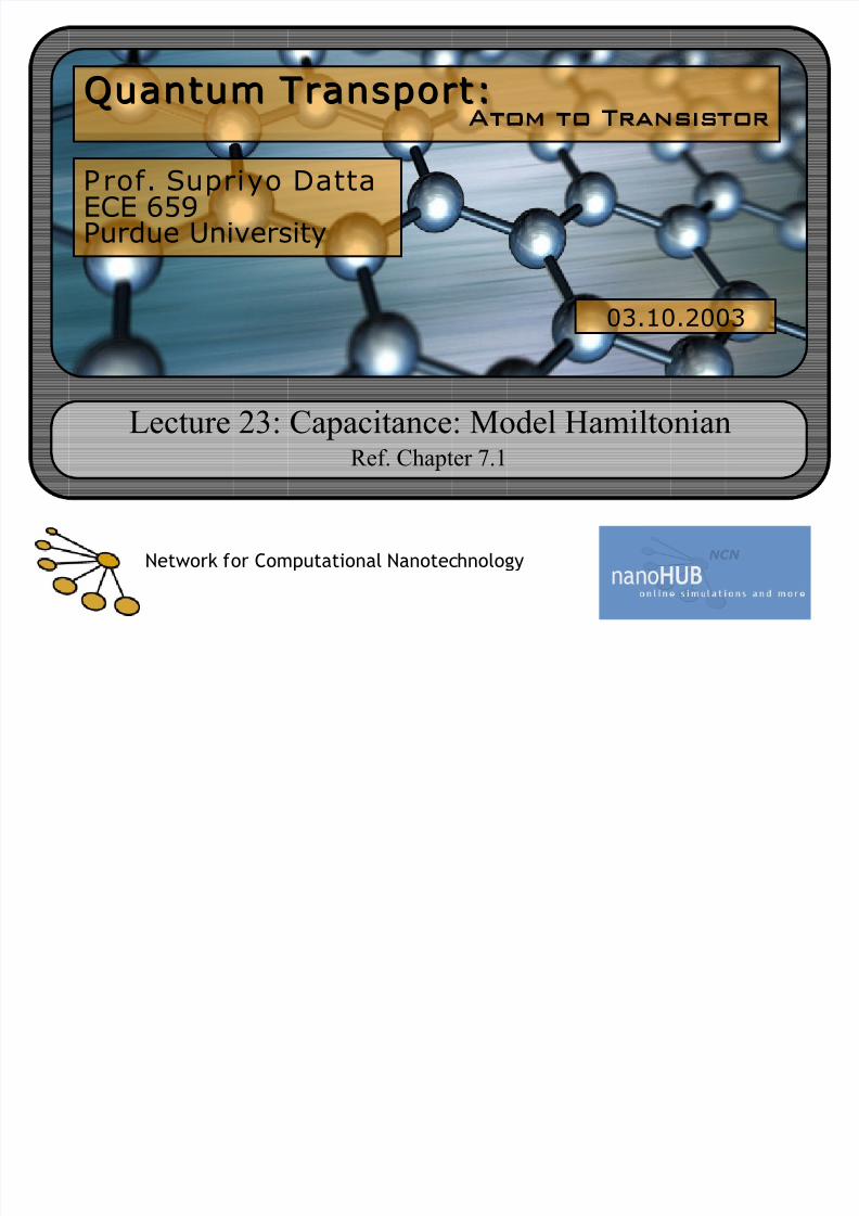
• At the beginning of this course we
started with a basic FET example
• In this simple model we discussed
the basic factors of current flow. Two
different levels for μ1 and μ2 in the
source and drain respectively resultsin the difference of agenda in the
contacts: one keeps pumping in
electrons while the other takes them
out which leads to a net flow of electrons, through a level ε.
• To make all this quantitative, we
need to understand 1) where the
levels in the channel are coming from
and how to model them; 2) how the
coupling to the contacts works.
h
2γ
ε
h1γ µ1
µ2
D
R
AI
N
S
O
U
R
CE
I
VG VDGate
INSULATOR
CHANNEL
L
INSULATOR
z
x
Introduction00:00
8/8/2019 Quantum Transport :Atom to Transistor,Capacitance: Model Hamiltonian
http://slidepdf.com/reader/full/quantum-transport-atom-to-transistorcapacitance-model-hamiltonian 3/14
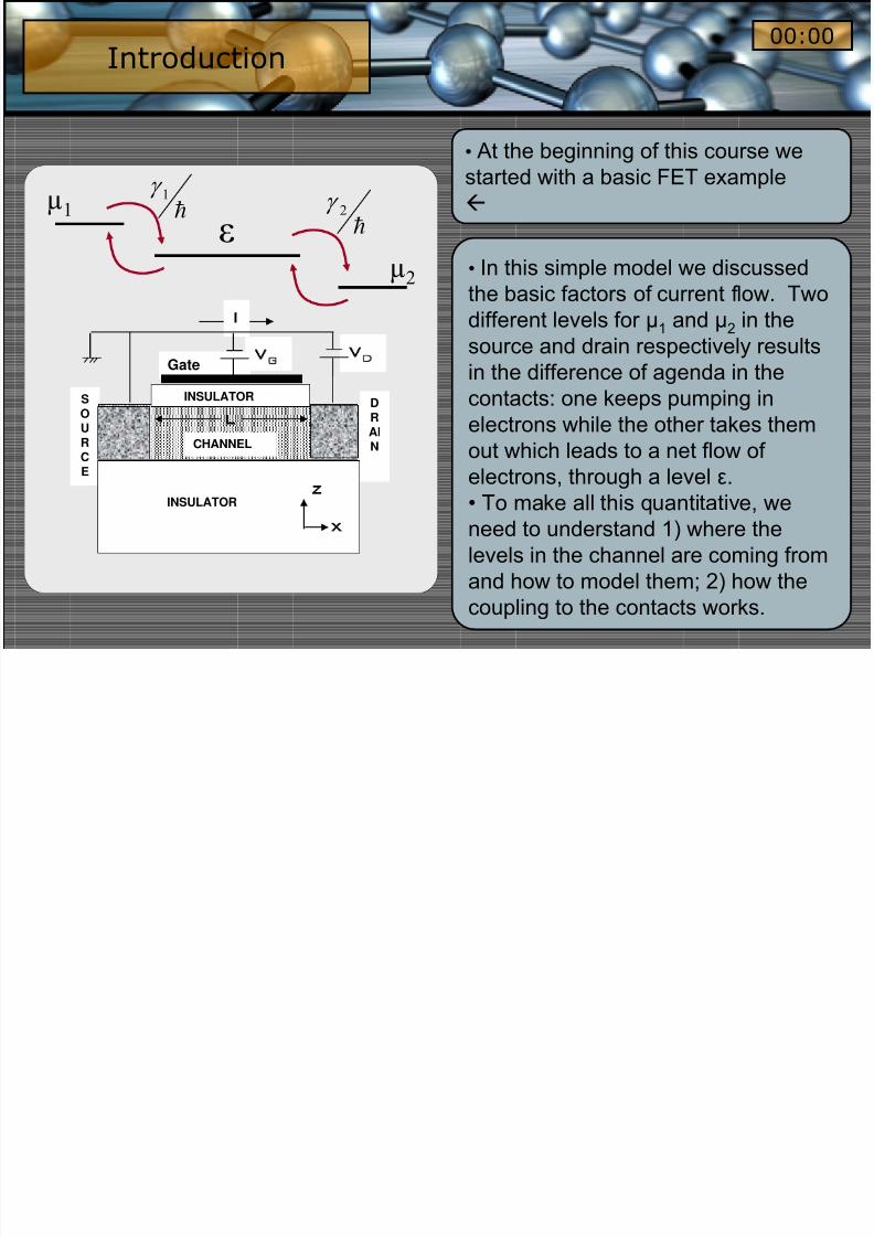
• This week we are going to derive
the Hamiltonian [H] for the FET
example. This matrix [H] replaces
the single number ε in the toy
example.
• From [H] we will show how to
calculate electron density in thechannel at equilibrium, that is
• Later on we will incorporate factorssuch as broadening and self-
consistent charging as we move
towards a non-equilibrium model.
( ) I H f μ ρ −= 0
FET Model
h2γ
εh
1γ
µ2
D
R
A
I
N
S
O
U
R
CE
I
VG VDGate
INSULATOR
CHANNEL
L
INSULATOR
z
x
µ1
Today we start by showing how to write H for the active region of a device.
Device Hamiltonian03:00
8/8/2019 Quantum Transport :Atom to Transistor,Capacitance: Model Hamiltonian
http://slidepdf.com/reader/full/quantum-transport-atom-to-transistorcapacitance-model-hamiltonian 4/14
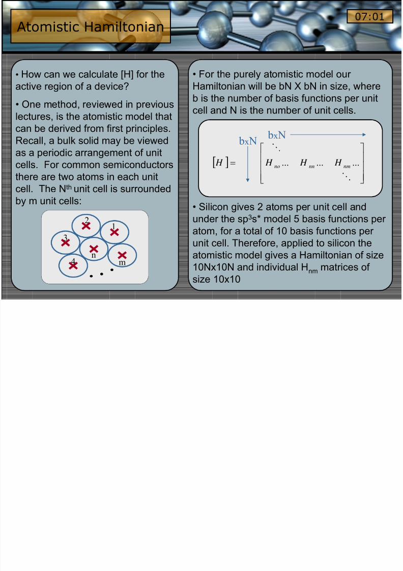
• How can we calculate [H] for the
active region of a device?
• One method, reviewed in previouslectures, is the atomistic model that
can be derived from first principles.
Recall, a bulk solid may be viewed
as a periodic arrangement of unit
cells. For common semiconductors
there are two atoms in each unit
cell. The Nth unit cell is surrounded
by m unit cells:
• For the purely atomistic model our
Hamiltonian will be bN X bN in size, where
b is the number of basis functions per unit
cell and N is the number of unit cells.
• Silicon gives 2 atoms per unit cell andunder the sp3s* model 5 basis functions per
atom, for a total of 10 basis functions per
unit cell. Therefore, applied to silicon the
atomistic model gives a Hamiltonian of size
10Nx10N and individual Hnm matrices of size 10x10
[ ]⎥⎥⎥
⎦
⎤
⎢⎢⎢
⎣
⎡
=
O
O
......... nmnnno H H H H
bx N bx N
n
m
12
3
4
Atomistic Hamiltonian07:01
8/8/2019 Quantum Transport :Atom to Transistor,Capacitance: Model Hamiltonian
http://slidepdf.com/reader/full/quantum-transport-atom-to-transistorcapacitance-model-hamiltonian 5/14
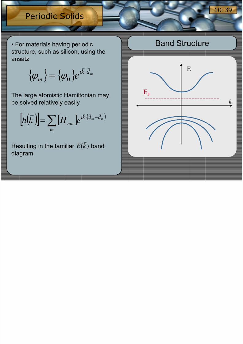
• For materials having periodic
structure, such as silicon, using the
ansatz
The large atomistic Hamiltonian maybe solved relatively easily
Resulting in the familiar band
diagram.
E
k
EF
Band Structure
{ } { } md k i
m evv⋅= 0ϕ ϕ
( )[ ] [ ] ( )∑ −⋅=m
d d k i
nmnme H k hvvvv
)(k E v
Periodic Solids10:39
8/8/2019 Quantum Transport :Atom to Transistor,Capacitance: Model Hamiltonian
http://slidepdf.com/reader/full/quantum-transport-atom-to-transistorcapacitance-model-hamiltonian 6/14
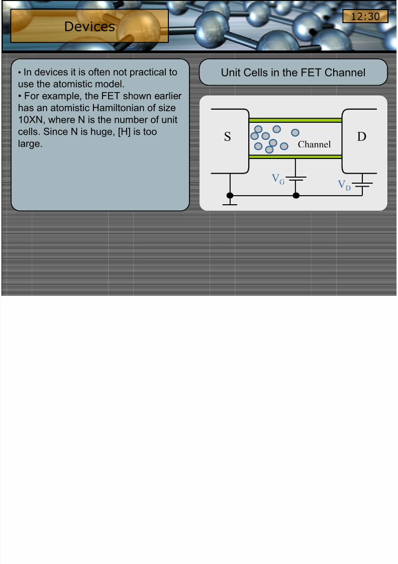
• In devices it is often not practical to
use the atomistic model.
• For example, the FET shown earlier
has an atomistic Hamiltonian of size10XN, where N is the number of unit
cells. Since N is huge, [H] is too
large.
Unit Cells in the FET Channel
ChannelDS
VG VD
Devices12:30
8/8/2019 Quantum Transport :Atom to Transistor,Capacitance: Model Hamiltonian
http://slidepdf.com/reader/full/quantum-transport-atom-to-transistorcapacitance-model-hamiltonian 7/14
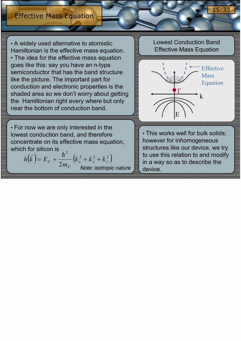
• A widely used alternative to atomistic
Hamiltonian is the effective mass equation.
• The idea for the effective mass equation
goes like this: say you have an n-typesemiconductor that has the band structure
like the picture. The important part for
conduction and electronic properties is the
shaded area so we don’t worry about gettingthe Hamiltonian right every where but only
near the bottom of conduction band.
• For now we are only interested in thelowest conduction band, and therefore
concentrate on its effective mass equation,
which for silicon is
Note: isotropic nature ( ) ( )222
2
2z y x
C
C k k k m
E k h +++=hv
Lowest Conduction Band
Effective Mass Equation
E
k Г
Effective
Mass
Equation
• This works well for bulk solids;
however for inhomogeneous
structures like our device, we try
to use this relation to and modifyin a way so as to describe the
device.
Effective Mass Equation15:33
8/8/2019 Quantum Transport :Atom to Transistor,Capacitance: Model Hamiltonian
http://slidepdf.com/reader/full/quantum-transport-atom-to-transistorcapacitance-model-hamiltonian 8/14
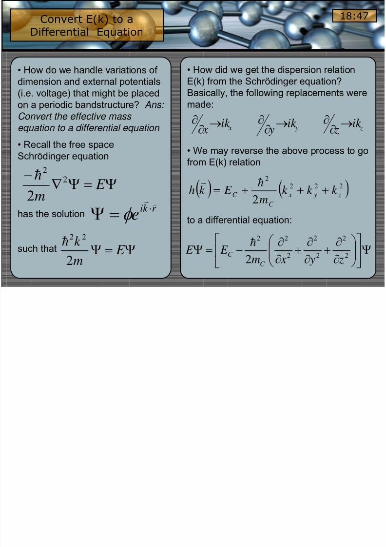
• How do we handle variations of
dimension and external potentials
(i.e. voltage) that might be placed
on a periodic bandstructure? Ans: Convert the effective mass
equation to a differential equation
• Recall the free space
Schrödinger equation
has the solution
such that
Ψ=Ψ∇−
E
m
22
2
h
r k ie
vv⋅=Ψ φ
Ψ=Ψ E m
k
2
22h
• How did we get the dispersion relation
E(k) from the Schrödinger equation?
Basically, the following replacements were
made:
• We may reverse the above process to gofrom E(k) relation
to a differential equation:
z y x ik z
ik y
ik x
→∂
∂→∂
∂→∂
∂
Ψ⎥⎦
⎤
⎢⎣
⎡
⎟⎟ ⎠
⎞
⎜⎜⎝
⎛
∂
∂
+∂
∂
+∂
∂
−=Ψ2
2
2
2
2
22
2 z y xm E E C
C
h
( ) ( )2222
2
z y x
C
C k k k
m
E k h +++=hv
Convert E(k) to aDifferential Equation
18:47
8/8/2019 Quantum Transport :Atom to Transistor,Capacitance: Model Hamiltonian
http://slidepdf.com/reader/full/quantum-transport-atom-to-transistorcapacitance-model-hamiltonian 9/14
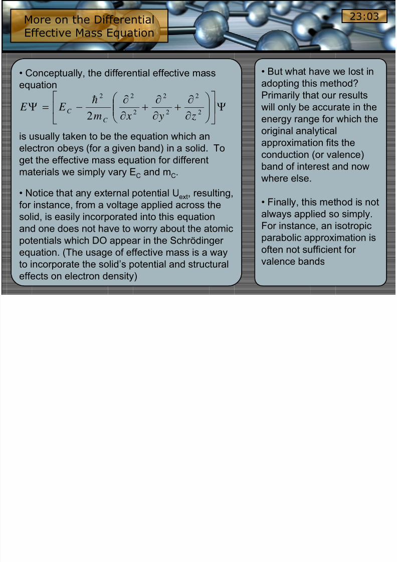
• Conceptually, the differential effective mass
equation
is usually taken to be the equation which an
electron obeys (for a given band) in a solid. To
get the effective mass equation for differentmaterials we simply vary EC and mC.
• Notice that any external potential Uext, resulting,
for instance, from a voltage applied across thesolid, is easily incorporated into this equation
and one does not have to worry about the atomic
potentials which DO appear in the Schrödinger
equation. (The usage of effective mass is a way
to incorporate the solid’s potential and structural
effects on electron density)
• But what have we lost in
adopting this method?
Primarily that our results
will only be accurate in theenergy range for which the
original analytical
approximation fits the
conduction (or valence)band of interest and now
where else.
• Finally, this method is not
always applied so simply.
For instance, an isotropic
parabolic approximation is
often not sufficient for
valence bands
Ψ⎥⎦
⎤⎢⎣
⎡⎟⎟ ⎠
⎞⎜⎜⎝
⎛
∂
∂+∂
∂+∂
∂−=Ψ 2
2
2
2
2
22
2 z y xm E E
C
C
h
More on the DifferentialEffective Mass Equation
23:03
8/8/2019 Quantum Transport :Atom to Transistor,Capacitance: Model Hamiltonian
http://slidepdf.com/reader/full/quantum-transport-atom-to-transistorcapacitance-model-hamiltonian 10/14
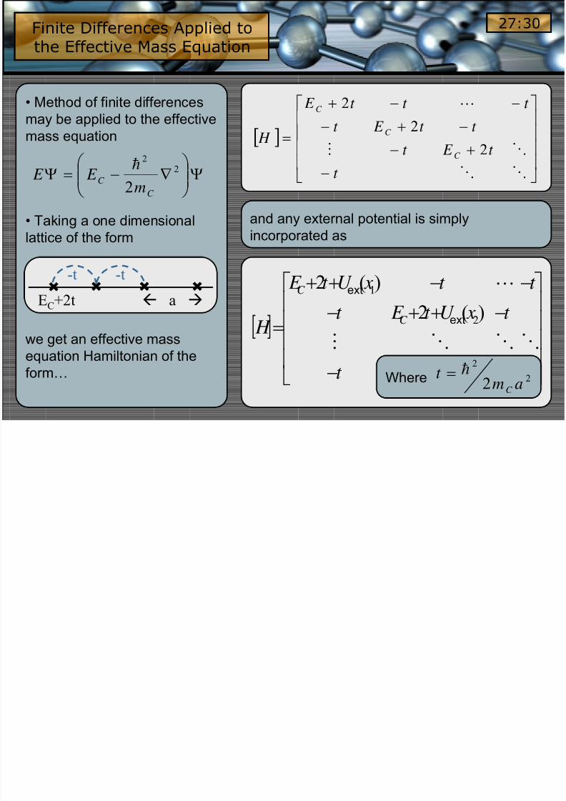
• Method of finite differences
may be applied to the effective
mass equation
• Taking a one dimensionallattice of the form
we get an effective mass
equation Hamiltonian of the
form…
and any external potential is simplyincorporated as
Ψ⎟⎟ ⎠
⎞⎜⎜⎝
⎛ ∇−=Ψ 2
2
2 C
C m
E E h
[ ]
⎥⎥
⎥⎥
⎦
⎤
⎢⎢
⎢⎢
⎣
⎡
−+−
−+−
−−+
=
OO
OM
L
t
t E t
t t E t
t t t E
H C
C
C
2
2
2
[ ]
⎥⎥⎥⎥
⎦
⎤
⎢⎢⎢⎢
⎣
⎡
−
−++−
−−++
=
OO
OOOM
L
t
t xU t E t
t t xU t E
H C
C
)(2
)(2
2
1
ext
ext
Where 2
2
2 amt C
h=
a
-t-t
EC+2t
Finite Differences Applied tothe Effective Mass Equation
27:30
8/8/2019 Quantum Transport :Atom to Transistor,Capacitance: Model Hamiltonian
http://slidepdf.com/reader/full/quantum-transport-atom-to-transistorcapacitance-model-hamiltonian 11/14
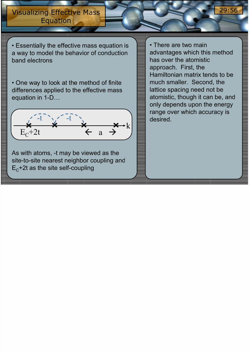
• Essentially the effective mass equation is
a way to model the behavior of conduction
band electrons
• One way to look at the method of finite
differences applied to the effective mass
equation in 1-D…
As with atoms, -t may be viewed as the
site-to-site nearest neighbor coupling andEC+2t as the site self-coupling
• There are two main
advantages which this method
has over the atomistic
approach. First, theHamiltonian matrix tends to be
much smaller. Second, the
lattice spacing need not be
atomistic, though it can be, andonly depends upon the energy
range over which accuracy is
desired.
a
-t-t
EC+2tk
Visualizing Effective MassEquation
29:56
8/8/2019 Quantum Transport :Atom to Transistor,Capacitance: Model Hamiltonian
http://slidepdf.com/reader/full/quantum-transport-atom-to-transistorcapacitance-model-hamiltonian 12/14
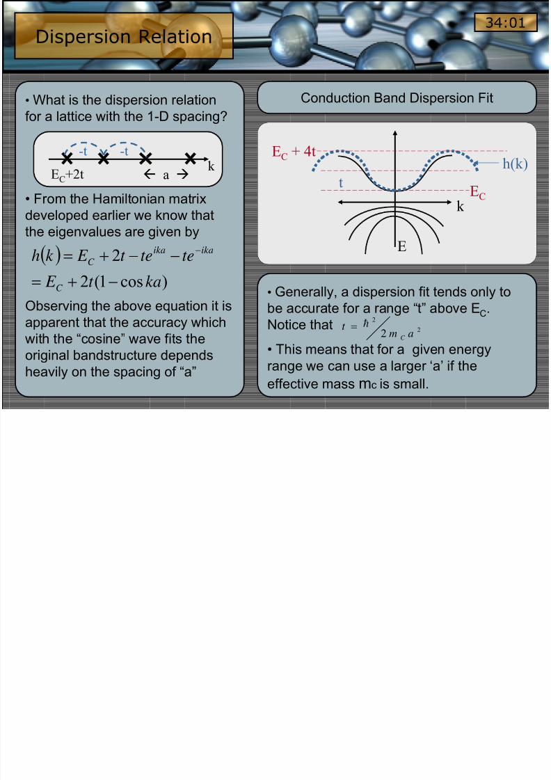
• What is the dispersion relation
for a lattice with the 1-D spacing?
• From the Hamiltonian matrix
developed earlier we know thatthe eigenvalues are given by
Observing the above equation it is
apparent that the accuracy which
with the “cosine” wave fits the
original bandstructure dependsheavily on the spacing of “a”
• Generally, a dispersion fit tends only tobe accurate for a range “t” above EC.
Notice that
• This means that for a given energy
range we can use a larger ‘a’ if the
effective mass mc is small.
Conduction Band Dispersion Fit
2
2
2 amt
C
h=
E
k
EC + 4t
EC
t
h(k) a
-t-t
EC+2tk
( )
)cos1(2
2
kat E
tetet E k h
C
ikaika
C
−+=
−−+= −
Dispersion Relation34:01
8/8/2019 Quantum Transport :Atom to Transistor,Capacitance: Model Hamiltonian
http://slidepdf.com/reader/full/quantum-transport-atom-to-transistorcapacitance-model-hamiltonian 13/14
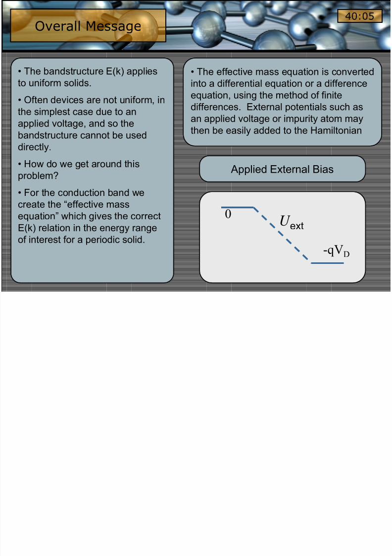
• The bandstructure E(k) applies
to uniform solids.
• Often devices are not uniform, inthe simplest case due to an
applied voltage, and so the
bandstructure cannot be used
directly.
• How do we get around this
problem?
• For the conduction band we
create the “effective massequation” which gives the correct
E(k) relation in the energy range
of interest for a periodic solid.
Applied External Bias
• The effective mass equation is converted
into a differential equation or a difference
equation, using the method of finite
differences. External potentials such asan applied voltage or impurity atom may
then be easily added to the Hamiltonian
0
-qVD
U ext
Overall Message40:05
8/8/2019 Quantum Transport :Atom to Transistor,Capacitance: Model Hamiltonian
http://slidepdf.com/reader/full/quantum-transport-atom-to-transistorcapacitance-model-hamiltonian 14/14
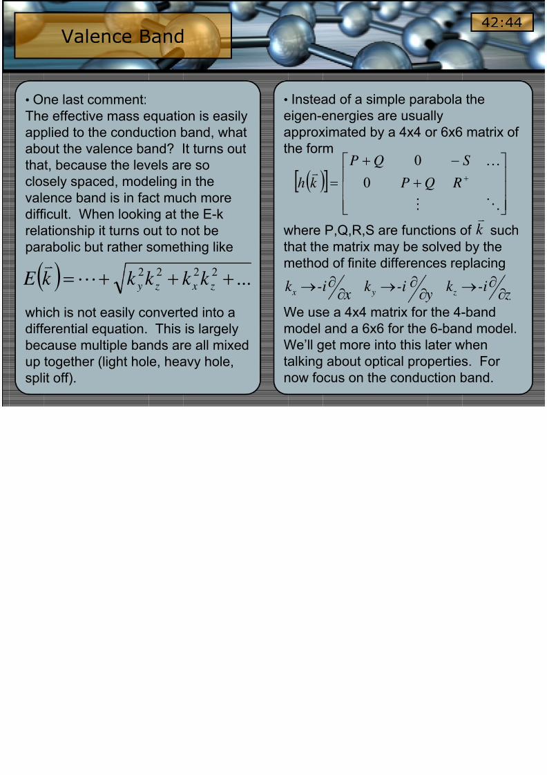
• One last comment:
The effective mass equation is easily
applied to the conduction band, what
about the valence band? It turns outthat, because the levels are so
closely spaced, modeling in the
valence band is in fact much more
difficult. When looking at the E-krelationship it turns out to not be
parabolic but rather something like
which is not easily converted into a
differential equation. This is largely
because multiple bands are all mixed
up together (light hole, heavy hole,split off).
• Instead of a simple parabola the
eigen-energies are usually
approximated by a 4x4 or 6x6 matrix of
the form
where P,Q,R,S are functions of such
that the matrix may be solved by the
method of finite differences replacing
We use a 4x4 matrix for the 4-band
model and a 6x6 for the 6-band model.
We’ll get more into this later when
talking about optical properties. For now focus on the conduction band.
( ) ...
2222 +++=z x z y k k k k k E
Lv
k v
z-ik y-ik x-ik z y x ∂∂→∂∂→∂∂→
( )[ ]⎥⎥⎥
⎦
⎤
⎢⎢⎢
⎣
⎡
+
−+
= +
OM
Kv
RQP
SQP
k h 0
0
Valence Band42:44