Embed Size (px)
Citation preview
© 2015 WILEY-VCH Verlag GmbH & Co. KGaA, Weinheim7908 wileyonlinelibrary.com
REV
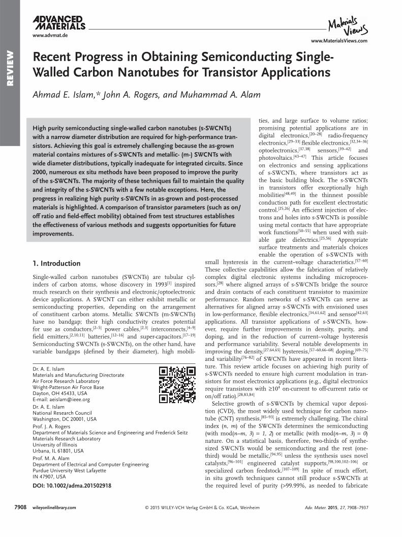
IEW Recent Progress in Obtaining Semiconducting Single-
Walled Carbon Nanotubes for Transistor Applications
Ahmad E. Islam ,* John A. Rogers , and Muhammad A. Alam
DOI: 10.1002/adma.201502918
ties, and large surface to volume ratios; promising potential applications are in digital electronics, [ 20–28 ] radio-frequency electronics, [ 29–33 ] fl exible electronics, [ 32,34–36 ] optoelectronics, [ 37,38 ] sensors, [ 39–42 ] and photovoltaics. [ 43–47 ] This article focuses on electronics and sensing applications of s-SWCNTs, where transistors act as the basic building block. The s-SWCNTs in transistors offer exceptionally high mobilities [ 48,49 ] in the thinnest possible conduction path for excellent electro static control. [ 25,26 ] An effi cient injection of elec-trons and holes into s-SWCNTs is possible using metal contacts that have appropriate work functions [ 50–55 ] when used with suit-able gate dielectrics. [ 25,56 ] Appropriate surface treatments and materials choices enable the operation of s-SWCNTs with
small hysteresis in the current–voltage characteristics. [ 57–60 ] These collective capabilities allow the fabrication of relatively complex digital electronic systems including microproces-sors, [ 28 ] where aligned arrays of s-SWCNTs bridge the source and drain contacts of each constituent transistor to maximize performance. Random networks of s-SWCNTs can serve as alternatives for aligned array s-SWCNTs with envisioned uses in low-performance, fl exible electronics, [ 34,61,62 ] and sensor [ 42,63 ] applications. All transistor applications of s-SWCNTs, how-ever, require further improvements in density, purity, and doping, and in the reduction of current–voltage hysteresis and performance variability. Several notable developments in improving the density, [ 27,64,65 ] hysteresis, [ 57–60,66–68 ] doping, [ 69–75 ] and variability [ 76–82 ] of SWCNTs have appeared in recent litera-ture. This review article focuses on achieving high purity of s-SWCNTs needed to ensure high current modulation in tran-sistors for most electronics applications (e.g., digital electronics require transistors with ≥10 4 on-current to off-current ratio or on/off ratio). [ 28,83,84 ]
Selective growth of s-SWCNTs by chemical vapor deposi-tion (CVD), the most widely used technique for carbon nano-tube (CNT) synthesis, [ 85–93 ] is extremely challenging. The chiral index ( n , m ) of the SWCNTs determines the semiconducting (with mod( n–m, 3 ) = 1, 2 ) or metallic (with mod( n–m, 3 ) = 0 ) nature. On a statistical basis, therefore, two-thirds of synthe-sized SWCNTs would be semiconducting and the rest (one-third) would be metallic, [ 94,95 ] unless the synthesis uses novel catalysts, [ 96–101 ] engineered catalyst supports, [ 98,100,102–106 ] or specialized carbon feedstock. [ 107–109 ] In spite of much effort, in situ growth techniques cannot still produce s-SWCNTs at the required level of purity (>99.99%, as needed to fabricate
High purity semiconducting single-walled carbon nanotubes (s-SWCNTs) with a narrow diameter distribution are required for high-performance tran-sistors. Achieving this goal is extremely challenging because the as-grown material contains mixtures of s-SWCNTs and metallic- (m-) SWCNTs with wide diameter distributions, typically inadequate for integrated circuits. Since 2000, numerous ex situ methods have been proposed to improve the purity of the s-SWCNTs. The majority of these techniques fail to maintain the quality and integrity of the s-SWCNTs with a few notable exceptions. Here, the progress in realizing high purity s-SWCNTs in as-grown and post-processed materials is highlighted. A comparison of transistor parameters (such as on/off ratio and fi eld-effect mobility) obtained from test structures establishes the effectiveness of various methods and suggests opportunities for future improvements.
Dr. A. E. Islam Materials and Manufacturing Directorate Air Force Research Laboratory Wright-Patterson Air Force Base Dayton , OH 45433 , USA E-mail: [email protected] Dr. A. E. Islam National Research Council Washington , DC 20001 , USA Prof. J. A. Rogers Department of Materials Science and Engineering and Frederick Seitz Materials Research Laboratory University of Illinois Urbana , IL 61801 , USA Prof. M. A. Alam Department of Electrical and Computer Engineering Purdue University West Lafayette IN 47907 , USA
1. Introduction
Single-walled carbon nanotubes (SWCNTs) are tubular cyl-inders of carbon atoms, whose discovery in 1993 [ 1 ] inspired much research on their synthesis and electronic/optoelectronic device applications. A SWCNT can either exhibit metallic or semiconducting properties, depending on the arrangement of constituent carbon atoms. Metallic SWCNTs (m-SWCNTs) have no bandgap; their high conductivity creates potential for use as conductors, [ 2–5 ] power cables, [ 2,3 ] interconnects, [ 4–9 ] fi eld emitters, [ 2,10,11 ] batteries, [ 12–16 ] and super-capacitors. [ 17–19 ] Semiconducting SWCNTs (s-SWCNTs), on the other hand, have variable bandgaps (defi ned by their diameter), high mobili-
Adv. Mater. 2015, 27, 7908–7937
www.advmat.dewww.MaterialsViews.com
7909wileyonlinelibrary.com© 2015 WILEY-VCH Verlag GmbH & Co. KGaA, Weinheim
REV
IEW
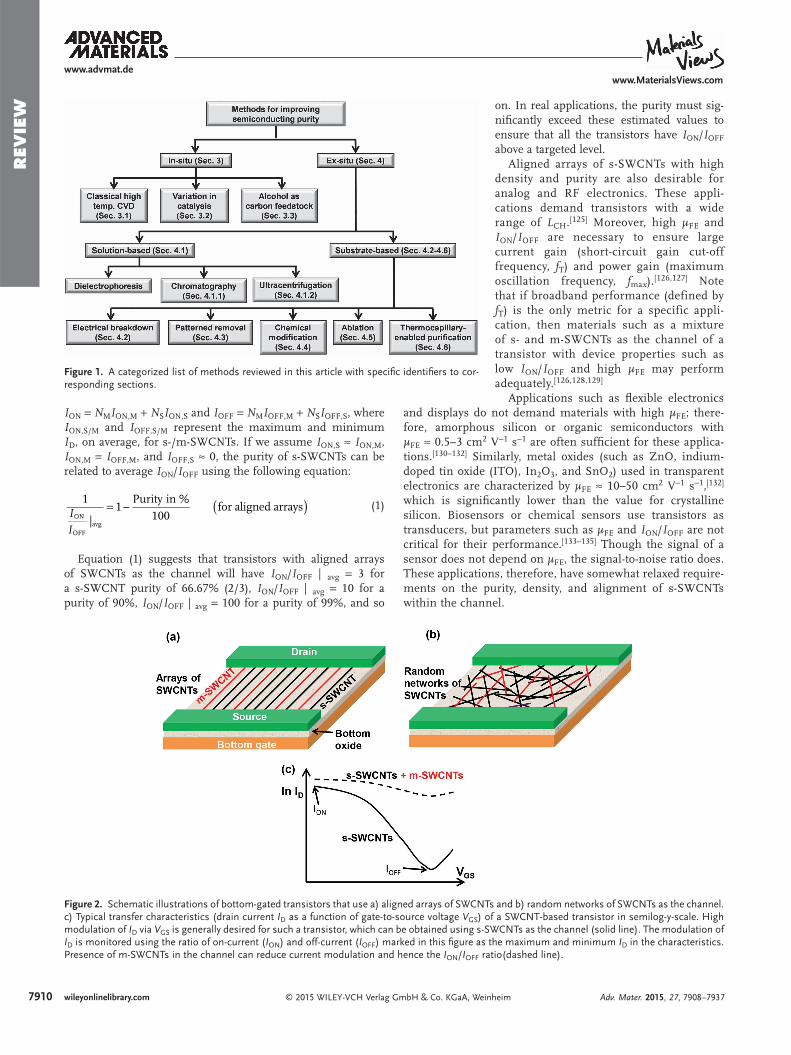
transistors with >10 4 on/off ratio based on aligned arrays of s-SWCNTs as the channel). [ 83 ] The ex situ removal of m-SWCNTs via post-processing, therefore, remains the only viable route to high purity s-SWCNTs. Recent review articles on such ex situ schemes [ 87,110–112 ] (including those that dis-cuss post-processing, along with other aspects of SWCNT electronics) [ 85,89,113,114 ] focus on the utility of selective chem-istry of SWCNTs (based on their chiral index) in different solutions to obtain different types of mono-disperse SWCNTs. These articles discuss methods for selective in situ growth of s-SWCNTs as supplementary to solution-based post-processing methods, while techniques such as electrical breakdown of m-SWCNTs [ 83,115 ] and selective chemical etching, [ 116 ] etc., are deemed impractical and/or ineffective. Recent research shows, however, successful use of electrical breakdown in nanoscale transistors, [ 64,117 ] even in large systems such as microproces-sors. [ 28 ] In addition, we have recently presented ex situ strate-gies that exploit nanoscale thermocapillary fl ows (thermocap-illary-enabled purifi cation; TcEP) [ 118–121 ] as a form of thermal lithography for complete removal of m-SWCNTs. This article summarizes both selective, in situ growth and ex situ, post-processing methods in the specifi c context of enabled electronic properties such as on/off ratio and charge transport character-istics. The methods discussed here are listed in Figure 1 , with specifi c identifi ers to corresponding sections. Section 2 pre-sents the required electronic properties for different transistor applications. Section 3 reviews CVD synthesis techniques with in situ modifi cations that improve the population of s-SWCNTs and compares the on/off ratios and charge transport properties of transistors made with such SWCNTs. Section 4 summarizes ex situ, post-processing methods with emphasis on the nature and scalability of their operation and electronic properties of transistors made with post-processed SWCNTs. A summary for in situ (Figure 9, Table 1) and ex situ (Figure 25, Table 2) methods allows easy comparisons.
2. Transistors with SWCNTs: Application Challenges
The SWCNTs that defi ne the channel of a transistor may be aligned parallel to the channel (aligned arrays of SWCNTs; Figure 2 a) or distributed randomly in a network confi guration (Figure 2 b). Aligned arrays of SWCNTs have the potential to replace crystalline channel materials (e.g., silicon, InGaAs) in digital, analog, and radio frequency (RF) electronics; random networks of SWCNTs, on the other hand, may replace amor-phous silicon and organic materials in fl exible electronics and fl at panel displays. In addition, SWCNTs can also be used in novel applications, such as transparent electronics, biosensors, and chemical sensors.
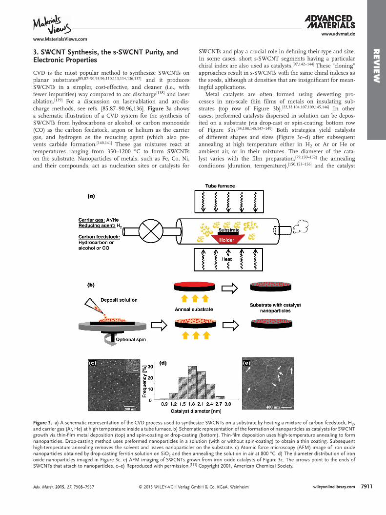
In digital electronics, silicon-based transistors operate with an on-current of ≈mA per µm width of the device and an on-current ( I ON ) to off-current ( I OFF ) ratio of >10 4 . [ 28,84,122,123 ] Specifi cally, I ON and I OFF are defi ned as the maximum and minimum drain current I D , respectively, during the sweep of gate to source voltage V GS by keeping a fi xed drain to source voltage V DS . To achieve the desired I ON and I ON / I OFF , one needs aligned arrays of s-SWCNTs as the channel
at densities, N S ≥ 100 per µm (defi ned as the number of SWCNTs per unit width of the transistor) and also needs a fi eld-effect mobility ( µ FE ≈ ∂ I D /∂ V GS | max ) comparable to that of silicon (≈500–1500 cm 2 V −1 s −1 ). [ 84,122,124 ] In this case, even a few m-SWCNTs (with density N M ) can degrade the purity of s-SWCNTs, defi ned as N S /( N S + N M ), and reduce I ON / I OFF signifi cantly (see Figure 2 c), as follows. [ 22,83,107,108 ] In a transistor with aligned arrays of SWCNTs as the channel,
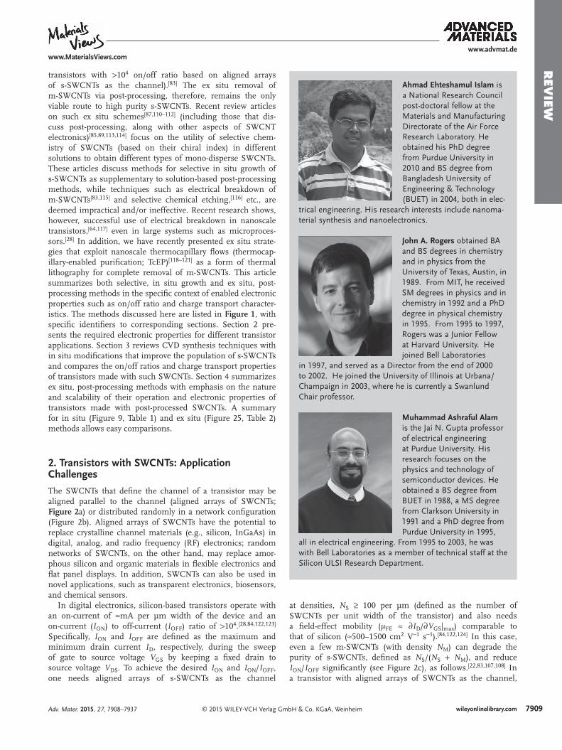
Ahmad Ehteshamul Islam is a National Research Council post-doctoral fellow at the Materials and Manufacturing Directorate of the Air Force Research Laboratory. He obtained his PhD degree from Purdue University in 2010 and BS degree from Bangladesh University of Engineering & Technology (BUET) in 2004, both in elec-
trical engineering. His research interests include nanoma-terial synthesis and nanoelectronics.
John A. Rogers obtained BA and BS degrees in chemistry and in physics from the University of Texas, Austin, in 1989. From MIT, he received SM degrees in physics and in chemistry in 1992 and a PhD degree in physical chemistry in 1995. From 1995 to 1997, Rogers was a Junior Fellow at Harvard University. He joined Bell Laboratories
in 1997, and served as a Director from the end of 2000 to 2002. He joined the University of Illinois at Urbana/Champaign in 2003, where he is currently a Swanlund Chair professor.
Muhammad Ashraful Alam is the Jai N. Gupta professor of electrical engineering at Purdue University. His research focuses on the physics and technology of semiconductor devices. He obtained a BS degree from BUET in 1988, a MS degree from Clarkson University in 1991 and a PhD degree from Purdue University in 1995,
all in electrical engineering. From 1995 to 2003, he was with Bell Laboratories as a member of technical staff at the Silicon ULSI Research Department.
Adv. Mater. 2015, 27, 7908–7937
www.advmat.dewww.MaterialsViews.com
7910 wileyonlinelibrary.com © 2015 WILEY-VCH Verlag GmbH & Co. KGaA, Weinheim
REV
IEW
I ON = N M I ON , M + N S I ON , S and I OFF = N M I OFF , M + N S I OFF , S , where I ON , S/M and I OFF , S/M represent the maximum and minimum I D , on average, for s-/m-SWCNTs. If we assume I ON , S ≈ I ON , M , I ON , M = I OFF , M , and I OFF , S ≈ 0, the purity of s-SWCNTs can be related to average I ON / I OFF using the following equation:
( )= −I
I
1
|1
Purity in %
100for aligned arrays
ON
OFFavg
(1)
Equation ( 1) suggests that transistors with aligned arrays of SWCNTs as the channel will have I ON / I OFF | avg = 3 for a s-SWCNT purity of 66.67% (2/3), I ON / I OFF | avg = 10 for a purity of 90%, I ON / I OFF | avg = 100 for a purity of 99%, and so
on. In real applications, the purity must sig-nifi cantly exceed these estimated values to ensure that all the transistors have I ON / I OFF above a targeted level.
Aligned arrays of s-SWCNTs with high density and purity are also desirable for analog and RF electronics. These appli-cations demand transistors with a wide range of L CH . [ 125 ] Moreover, high µ FE and I ON / I OFF are necessary to ensure large current gain (short-circuit gain cut-off frequency, f T ) and power gain (maximum oscillation frequency, f ma x ). [ 126,127 ] Note that if broadband performance (defined by f T ) is the only metric for a specific appli-cation, then materials such as a mixture of s- and m-SWCNTs as the channel of a transistor with device properties such as low I ON / I OFF and high µ FE may perform adequately. [ 126,128,129 ]
Applications such as fl exible electronics and displays do not demand materials with high µ FE ; there-fore, amorphous silicon or organic semiconductors with µ FE ≈ 0.5–3 cm 2 V −1 s −1 are often suffi cient for these applica-tions. [ 130–132 ] Similarly, metal oxides (such as ZnO, indium-doped tin oxide (ITO), In 2 O 3 , and SnO 2 ) used in transparent electronics are characterized by µ FE ≈ 10–50 cm 2 V −1 s −1 , [ 132 ] which is signifi cantly lower than the value for crystalline silicon. Biosensors or chemical sensors use transistors as transducers, but parameters such as µ FE and I ON / I OFF are not critical for their performance. [ 133–135 ] Though the signal of a sensor does not depend on µ FE , the signal-to-noise ratio does. These applications, therefore, have somewhat relaxed require-ments on the purity, density, and alignment of s-SWCNTs within the channel.
Adv. Mater. 2015, 27, 7908–7937
www.advmat.dewww.MaterialsViews.com
Figure 1. A categorized list of methods reviewed in this article with specifi c identifi ers to cor-responding sections.
Figure 2. Schematic illustrations of bottom-gated transistors that use a) aligned arrays of SWCNTs and b) random networks of SWCNTs as the channel. c) Typical transfer characteristics (drain current I D as a function of gate-to-source voltage V GS ) of a SWCNT-based transistor in semilog-y-scale. High modulation of I D via V GS is generally desired for such a transistor, which can be obtained using s-SWCNTs as the channel (solid line). The modulation of I D is monitored using the ratio of on-current ( I ON ) and off-current ( I OFF ) marked in this fi gure as the maximum and minimum I D in the characteristics. Presence of m-SWCNTs in the channel can reduce current modulation and hence the I ON / I OFF ratio(dashed line).
7911wileyonlinelibrary.com© 2015 WILEY-VCH Verlag GmbH & Co. KGaA, Weinheim
REV
IEW
3. SWCNT Synthesis, the s-SWCNT Purity, and Electronic Properties
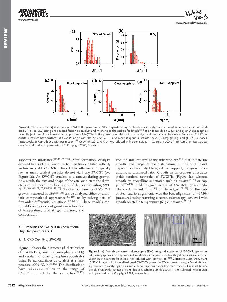
CVD is the most popular method to synthesize SWCNTs on planar substrates [ 85,87–90,93,96,110,113,114,136,137 ] and it produces SWCNTs in a simpler, cost-effective, and cleaner (i.e., with fewer impurities) way compared to arc discharge [ 138 ] and laser ablation. [ 139 ] For a discussion on laser-ablation and arc-dis-charge methods, see refs. [ 85,87–90,96,136 ] . Figure 3 a shows a schematic illustration of a CVD system for the synthesis of SWCNTs from hydrocarbons or alcohol, or carbon monooxide (CO) as the carbon feedstock, argon or helium as the carrier gas, and hydrogen as the reducing agent (which also pre-vents carbide formation. [ 140,141 ] These gas mixtures react at temperatures ranging from 350–1200 °C to form SWCNTs on the substrate. Nanoparticles of metals, such as Fe, Co, Ni, and their compounds, act as nucleation sites or catalysts for
SWCNTs and play a crucial role in defi ning their type and size. In some cases, short s-SWCNT segments having a particular chiral index are also used as catalysts. [ 97,142–144 ] These “cloning” approaches result in s-SWCNTs with the same chiral indexes as the seeds, although at densities that are insignifi cant for mean-ingful applications.
Metal catalysts are often formed using dewetting pro-cesses in nm-scale thin fi lms of metals on insulating sub-strates (top row of Figure 3 b). [ 22,33,104,107,109,145,146 ] In other cases, preformed catalysts dispersed in solution can be depos-ited on a substrate (via drop-cast or spin-coating; bottom row of Figure 3 b). [ 34,108,145,147–149 ] Both strategies yield catalysts of different shapes and sizes (Figure 3 c–d) after subsequent annealing at high temperature either in H 2 or Ar or He or ambient air, or in their mixtures. The diameter of the cata-lyst varies with the fi lm preparation, [ 79,150–152 ] the annealing conditions (duration, temperature), [ 150,153–156 ] and the catalyst
Adv. Mater. 2015, 27, 7908–7937
www.advmat.dewww.MaterialsViews.com
Figure 3. a) A schematic representation of the CVD process used to synthesize SWCNTs on a substrate by heating a mixture of carbon feedstock, H 2 , and carrier gas (Ar, He) at high temperature inside a tube furnace. b) Schematic representation of the formation of nanoparticles as catalysts for SWCNT growth via thin-fi lm metal deposition (top) and spin-coating or drop-casting (bottom). Thin-fi lm deposition uses high-temperature annealing to form nanoparticles. Drop-casting method uses preformed nanoparticles in a solution (with or without spin-coating) to obtain a thin coating. Subsequent high-temperature annealing removes the solvent and leaves nanoparticles on the substrate. c) Atomic force microscopy (AFM) image of iron oxide nanoparticles obtained by drop-casting ferritin solution on SiO 2 and then annealing the solution in air at 800 °C. d) The diameter distribution of iron oxide nanoparticles imaged in Figure 3 c. e) AFM imaging of SWCNTs grown from iron oxide catalysts of Figure 3 c. The arrows point to the ends of SWCNTs that attach to nanoparticles. c–e) Reproduced with permission. [ 151 ] Copyright 2001, American Chemical Society.
7912 wileyonlinelibrary.com © 2015 WILEY-VCH Verlag GmbH & Co. KGaA, Weinheim
REV
IEW
supports or substrates. [ 153,154,157,158 ] After formation, catalysts exposed to a suitable fl ow of carbon feedstock diluted with H 2 and/or Ar yield SWCNTs. The catalytic effi ciency is typically low, as many catalyst particles do not yield any SWCNT (see Figure 3 d). An SWCNT attaches to a catalyst during growth. As a result, the size and shape of the catalyst dictate the diam-eter and infl uence the chiral index of the corresponding SWCNT. [ 98,100,102,103,105,110,155,159,160 ] The chemical kinetics of SWCNT growth measured in situ [ 161–165 ] can be analyzed either by atom-istic computational approaches [ 166–169 ] or by solving sets of fi rst-order differential equations. [ 165,170,171 ] These models cap-ture different aspects of growth as a function of temperature, catalyst, gas pressure, and composition.
3.1. Properties of SWCNTs in Conventional High-Temperature CVD
3.1.1. CVD Growth of SWCNTs
Figure 4 shows the diameter ( d ) distribution of SWCNTs grown on amorphous (SiO 2 ) and crystalline (quartz, sapphire) substrates using Fe nanoparticles as catalyst at a tem-perature ≥900 °C. [ 79,151,152 ] The distributions have minimum values in the range of 0.5–0.7 nm, set by the energetics [ 172,173 ]
and the smallest size of the fullerene cap [ 174 ] that initiate the growth. The range of the distribution, on the other hand, depends on the catalyst type, catalyst support, and growth con-ditions, as discussed later. Growth on amorphous substrates yields random networks of SWCNTs ( Figure 5 a), whereas growth on crystalline substrates such as quartz [ 22,175 ] or sap-phire [ 176–178 ] yields aligned arrays of SWCNTs (Figure 5 b). The crystal orientations [ 146 ] or step-edges [ 177,179 ] on the sub-strates lead to alignment, with the best alignment of >99.9% (measured using scanning electron microscopy) achieved with growth on stable temperature (ST)-cut quartz. [ 22,180 ]
Adv. Mater. 2015, 27, 7908–7937
www.advmat.dewww.MaterialsViews.com
Figure 4. The diameter ( d ) distribution of SWCNTs grown a) on ST-cut quartz using Fe thin-fi lm as catalyst and ethanol vapor as the carbon feed-stock, [ 79 ] b) on SiO 2 using drop-casted ferritin as catalyst and methane as the carbon feedstock, [ 151 ] c) on R-cut, d) on C-cut, and e) on A-cut sapphire using Fe (obtained from thermal decomposition of Fe(CO) 5 in the presence of oleic acid) as catalyst and methane as the carbon feedstock. [ 152 ] ST-cut quartz substrate have surfaces at a 42°45′ angle with the Y-plane; R-, C-, and A-cut sapphire substrates have (1–102), (0001), and (11–20) surfaces, respectively. a) Reproduced with permission. [ 79 ] Copyright 2012, AIP. b) Reproduced with permission. [ 151 ] Copyright 2001, American Chemical Society. c–e) Reproduced with permission. [ 152 ] Copyright 2005, Elsevier.
Figure 5. a) Scanning electron microscopy (SEM) image of networks of SWCNTs grown on SiO 2 using spin-coated Fe/Co-based solutions as the precursor to catalyst particles and ethanol vapor as the carbon feedstock. Reproduced with permission. [ 181 ] Copyright 2006 Wiley-VCH. b) SEM image of horizontally-aligned SWCNTs grown on ST-cut quartz using a Fe thin-fi lm as a precursor to catalyst particles and ethanol vapor as the carbon feedstock. [ 22 ] The inset (inside the blue rectangle) shows a magnifi ed area where a single SWCNT is misaligned. Reproduced with permission. [ 22 ] Copyright 2007, Macmillan.
7913wileyonlinelibrary.com© 2015 WILEY-VCH Verlag GmbH & Co. KGaA, Weinheim
REV
IEW
3.1.2. Electronic Characterization of Aligned Arrays of SWCNTs
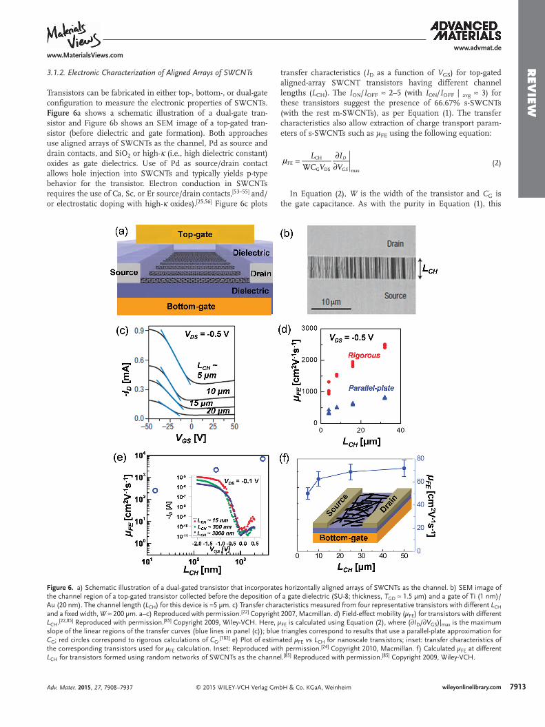
Transistors can be fabricated in either top-, bottom-, or dual-gate confi guration to measure the electronic properties of SWCNTs. Figure 6 a shows a schematic illustration of a dual-gate tran-sistor and Figure 6 b shows an SEM image of a top-gated tran-sistor (before dielectric and gate formation). Both approaches use aligned arrays of SWCNTs as the channel, Pd as source and drain contacts, and SiO 2 or high-κ (i.e., high dielectric constant) oxides as gate dielectrics. Use of Pd as source/drain contact allows hole injection into SWCNTs and typically yields p-type behavior for the transistor. Electron conduction in SWCNTs requires the use of Ca, Sc, or Er source/drain contacts, [ 53–55 ] and/or electrostatic doping with high-κ oxides). [ 25,56 ] Figure 6 c plots
transfer characteristics ( I D as a function of V GS ) for top-gated aligned-array SWCNT transistors having different channel lengths ( L CH ). The I ON / I OFF ≈ 2–5 (with I ON / I OFF | avg ≈ 3) for these transistors suggest the presence of 66.67% s-SWCNTs (with the rest m-SWCNTs), as per Equation ( 1) . The transfer characteristics also allow extraction of charge transport param-eters of s-SWCNTs such as µ FE using the following equation:
WC
FECH
G DS max
L
V
I
VD
GS
μ = ∂∂
(2)
In Equation ( 2) , W is the width of the transistor and C G is the gate capacitance. As with the purity in Equation ( 1) , this
Adv. Mater. 2015, 27, 7908–7937
www.advmat.dewww.MaterialsViews.com
Figure 6. a) Schematic illustration of a dual-gated transistor that incorporates horizontally aligned arrays of SWCNTs as the channel. b) SEM image of the channel region of a top-gated transistor collected before the deposition of a gate dielectric (SU-8; thickness, T GD ≈ 1.5 µm) and a gate of Ti (1 nm)/Au (20 nm). The channel length ( L CH ) for this device is ≈5 µm. c) Transfer characteristics measured from four representative transistors with different L CH and a fi xed width, W ≈ 200 µm. a–c) Reproduced with permission. [ 22 ] Copyright 2007, Macmillan. d) Field-effect mobility ( µ FE ) for transistors with different L CH . [ 22,85 ] Reproduced with permission. [ 85 ] Copyright 2009, Wiley-VCH. Here, µ FE is calculated using Equation ( 2) , where (∂ I D /∂ V GS )| max is the maximum slope of the linear regions of the transfer curves (blue lines in panel (c)); blue triangles correspond to results that use a parallel-plate approximation for C G ; red circles correspond to rigorous calculations of C G . [ 182 ] e) Plot of estimated µ FE vs L CH for nanoscale transistors; inset: transfer characteristics of the corresponding transistors used for µ FE calculation. Inset: Reproduced with permission. [ 24 ] Copyright 2010, Macmillan. f) Calculated µ FE at different L CH for transistors formed using random networks of SWCNTs as the channel. [ 85 ] Reproduced with permission. [ 85 ] Copyright 2009, Wiley-VCH.
7914 wileyonlinelibrary.com © 2015 WILEY-VCH Verlag GmbH & Co. KGaA, Weinheim
REV
IEW approach to calculate µ FE also presumes negligible current mod-
ulation for the m-SWCNTs. When C G is calculated using a par-allel-plate model (valid for transistors with thick gate dielectric and/or with high density of s-SWCNTs as the channel [ 182 ] ), µ FE is ≈1000 cm 2 V −1 s −1 for L CH ≈ 30 µm (Figure 6 d). A proper cal-culation of C G accounts for s-SWCNT density and the associated fringing fi eld effects [ 22,182 ] and suggests µ FE > 1000 cm 2 V −1 s −1 for L CH > 300 nm (Figure 6 d,e). Irrespective of the methods used to calculate C G , the extracted µ FE decreases with decreasing L CH due to effects associated with parasitic contact resistances at the metal–s-SWCNT interfaces, which can dominate over the channel resistance at small L CH . [ 24,50,52,85 ]
3.1.3. Electronic Characterization of Randomly Oriented SWCNTs
Current–voltage measurements on transistors built using random networks of SWCNTs as the channel and with
rigorous calculation of C G suggests µ FE ≈ 70 cm 2 V −1 s −1 for large L CH (Figure 6 f)– a signifi cantly lower value compared to that in transistors with aligned arrays of SWCNTs as the channel. The L CH dependence of µ FE in Figure 6 f arises from the effects of parasitic resistances at the metal–s-SWCNT contacts, as discussed previously, and at the SWCNT–SWCNT junctions. [ 183 ] Transistors with network SWCNTs also show an I ON / I OFF ratio that varies widely (contrary to a small variation in I ON / I OFF ≈ 2–5 for transistors with aligned arrays of SWCNTs) from 10 0 –10 1 in transistors with high density (>35 µm −2 ) SWCNTs to 10 3 –10 5 in transistors with low density SWCNTs. [ 34,184,185 ] The lack of current percola-tion from source to drain through m-SWCNTs results in a high I ON / I OFF ratio in low density network transistors. [ 184 ] Table 1 summarizes these electrical parameters, along with growth conditions and s-SWCNT purity, and compares them to values obtained with improved SWCNT synthesis methods discussed later.
Adv. Mater. 2015, 27, 7908–7937
www.advmat.dewww.MaterialsViews.com
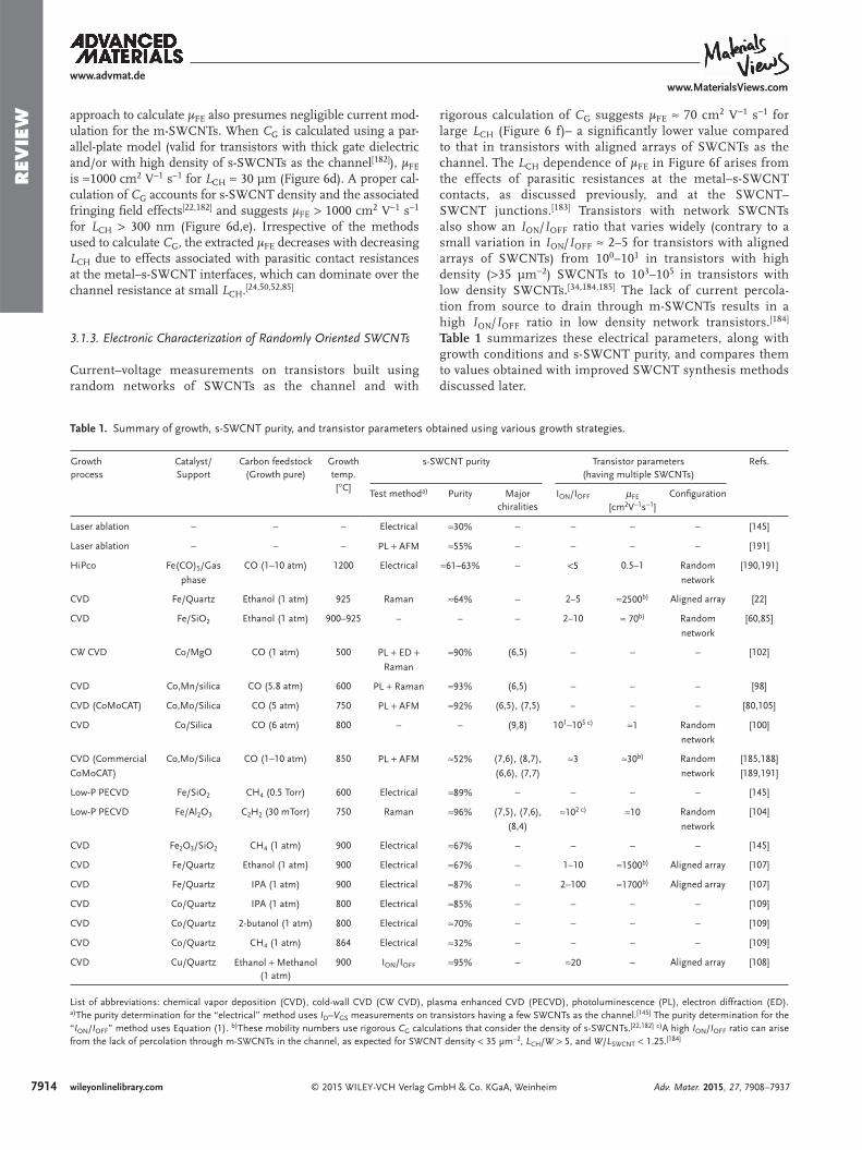
Table 1. Summary of growth, s-SWCNT purity, and transistor parameters obtained using various growth strategies.
Growth process
Catalyst/ Support
Carbon feedstock (Growth pure)
Growth temp. [°C]
s-SWCNT purity Transistor parameters (having multiple SWCNTs)
Refs.
Test method a) Purity Major chiralities
I ON /I OFF μ FE [cm 2 V −1 s −1 ]
Confi guration
Laser ablation – – – Electrical ≈30% – – – – [145]
Laser ablation – – – PL + AFM ≈55% – – – – [191]
HiPco Fe(CO) 5 /Gas
phase
CO (1–10 atm) 1200 Electrical ≈61–63% – <5 0.5–1 Random
network
[190,191]
CVD Fe/Quartz Ethanol (1 atm) 925 Raman ≈64% – 2–5 ≈2500 b) Aligned array [22]
CVD Fe/SiO 2 Ethanol (1 atm) 900–925 – – – 2–10 ≈ 70 b) Random
network
[60,85]
CW CVD Co/MgO CO (1 atm) 500 PL + ED +
Raman
≈90% (6,5) – – – [102]
CVD Co,Mn/silica CO (5.8 atm) 600 PL + Raman ≈93% (6,5) – – – [98]
CVD (CoMoCAT) Co,Mo/Silica CO (5 atm) 750 PL + AFM ≈92% (6,5), (7,5) – – – [80,105]
CVD Co/Silica CO (6 atm) 800 – – (9,8) 10 1 –10 5 c) ≈1 Random
network
[100]
CVD (Commercial
CoMoCAT)
Co,Mo/Silica CO (1–10 atm) 850 PL + AFM ≈52% (7,6), (8,7),
(6,6), (7,7) ≈3 ≈30 b) Random
network
[ 185,188 ]
[ 189,191 ]
Low-P PECVD Fe/SiO 2 CH 4 (0.5 Torr) 600 Electrical ≈89% – – – – [145]
Low-P PECVD Fe/Al 2 O 3 C 2 H 2 (30 mTorr) 750 Raman ≈96% (7,5), (7,6),
(8,4)≈10 2 c) ≈10 Random
network
[104]
CVD Fe 2 O 3 /SiO 2 CH 4 (1 atm) 900 Electrical ≈67% – – – – [145]
CVD Fe/Quartz Ethanol (1 atm) 900 Electrical ≈67% – 1–10 ≈1500 b) Aligned array [107]
CVD Fe/Quartz IPA (1 atm) 900 Electrical ≈87% – 2–100 ≈1700 b) Aligned array [107]
CVD Co/Quartz IPA (1 atm) 800 Electrical ≈85% – – – – [109]
CVD Co/Quartz 2-butanol (1 atm) 800 Electrical ≈70% – – – – [109]
CVD Co/Quartz CH 4 (1 atm) 864 Electrical ≈32% – – – – [109]
CVD Cu/Quartz Ethanol + Methanol (1 atm)
900 I ON /I OFF ≈95% – ≈20 – Aligned array [108]
List of abbreviations: chemical vapor deposition (CVD), cold-wall CVD (CW CVD), plasma enhanced CVD (PECVD), photoluminescence (PL), electron diffraction (ED). a) The purity determination for the “electrical” method uses I D – V GS measurements on transistors having a few SWCNTs as the channel. [ 145 ] The purity determination for the “ I ON / I OFF ” method uses Equation ( 1) . b) These mobility numbers use rigorous C G calculations that consider the density of s-SWCNTs. [ 22,182 ] c) A high I ON / I OFF ratio can arise from the lack of percolation through m-SWCNTs in the channel, as expected for SWCNT density < 35 µm −2 , L CH / W > 5, and W / L SWCNT < 1.25. [ 184 ]
7915wileyonlinelibrary.com© 2015 WILEY-VCH Verlag GmbH & Co. KGaA, Weinheim
REV
IEW
3.2. Properties of SWCNTs Grown Using Heterogeneous Catalysis
The I ON / I OFF ratio in transistors made with aligned arrays of SWCNTs or with high density random networks can be improved through the use of heterogeneous catalysis for SWCNT growth. Control in the composition, shape, and size of the metal catalysts available using heterogeneous catalysis enables the synthesis of improved purity of s-SWCNTs with a narrowed diameter distribution. In general, heterogeneous catalysis requires the use of active oxide supports such as silica (SiO x ), alumina (AlO x ), and magnesium oxide (MgO) that have a high porosity, surface area, and basicity. [ 96,102,104,153,158,186–189 ] These properties ensure strong interactions with the catalyst and hence enhanced dispersion and stability of the catalyst during growth.
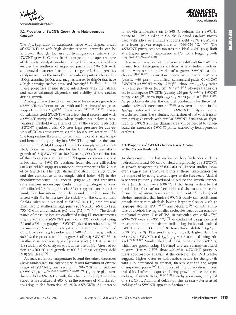
Among different metal catalysts used for selective growth of s-SWCNTs, Co forms catalysts with uniform size and shape on supports such as MgO [ 102,189 ] and silica. [ 98,100,103,105,189 ] These Co catalysts yield SWCNTs with a few chiral indices and with s-SWCNT purity of ≥90%, when synthesized below a tem-perature threshold with a fl ow of CO as the carbon feedstock. (SWCNT synthesis with CO uses high pressure for conver-sion of CO to active carbon via the Boudouard reaction. [ 190 ] ) The temperature threshold to maintain the catalyst size/shape and hence the high purity in s-SWCNTs depends on the cata-lyst support. A MgO support interacts strongly with the cat-alyst, forms anchoring sites for the Co catalysts, and allows growth of (6,5)-SWCNTs at 500 °C using CO after calcination of the Co catalysts at 1000 °C. [ 102 ] Figure 7 a shows a chiral index map of SWCNTs obtained from electron diffraction analysis, which suggests semiconducting properties for 51 out of 57 SWCNTs. The tight diameter distribution (Figure 7 b) and the dominance of the single chiral index (6,5) in the photoluminescence (PL) spectra (Figure 7 c) and transmis-sion electron microscopy confi rm the high degree of con-trol afforded by this approach. Silica supports, on the other hand, have low interaction with Co and, therefore, must be mixed with Mo to increase the stability of the catalyst. This Co/Mo mixture is reduced at 500 °C in a H 2 ambient and then used to synthesize high purity (CoMoCAT) s-SWCNTs at 750 °C with chiral indices (6,5) and (7,5). [ 103,105,189 ] The domi-nance of these indices are confi rmed using PL measurements (Figure 7 d) and a s-SWCNT purity of ≈92% is detected using PL and AFM topography of SWCNTs placed on mica slides. [ 191 ] (In one case, Mn in the catalyst support stabilizes the size of Co catalysts during H 2 reduction at 700 °C and then growth at 600 °C; the process results in growth of (6,5) SWCNTs. [ 98 ] In another case, a special type of porous silica (TUD-1) ensures the stability of Co catalysts without the use of Mo. After reduc-tion at ≈500 °C and growth at 800 °C, these catalysts yield (9,8) SWCNTs. [ 100 ]
An increase in the temperature beyond the values discussed above randomizes the catalyst size, favors formation of diverse range of SWCNTs, and results in SWCNTs with reduced s-SWCNT purity. [ 98,100,103,105,110,159,160,188,191 ] Figure 7 e plots sim-ilar trends for SWCNT growth, for which a Co catalyst on silica supports is stabilized at 600 °C in the presence of Mn, thereby resulting in the formation of ≈93% s-SWCNTs. An increase
in growth temperature up to 800 °C reduces the s-SWCNT purity to ≈61%. Similar to Co, the Fe-based catalysts mostly used with silica or alumina supports yield ≈90% s-SWCNTs at a lower growth temperature of ≈600–750 °C. [ 104,145 ] The s-SWCNT purity reduces towards the ideal ≈67% (2/3) limit at a higher growth temperature and/or for a longer growth time. [ 22,34,99,104,107,148,181 ]
Transistor characterization is generally diffi cult for SWCNTs formed from heterogeneous catalysis. A few studies use tran-sistors with random networks of as-grown SWCNTs as the channel. [ 100,104,185 ] Transistors made with dense SWCNTs (density ≈60 µm −2 ; unpurifi ed, commercial-grade CoMoCAT SWCNTs; s-SWCNT purity ≈52%) [ 191 ] show low I ON / I OFF ratios (≈ 3) and µ FE values (≈30 cm 2 V −1 s −1 ), [ 185 ] whereas transistors made with sparse SWCNTs (density ≤20 µm −2 , [ 100,104 ] s-SWCNT purity ≈96%) [ 104 ] show high I ON / I OFF ratios (≈10 1 –10 5 ). [ 100,104,185 ] As percolation dictates the channel conduction for these net-worked SWCNT transistors, [ 34,184,185 ] a systematic trend in the I ON / I OFF ratio with variation in s-SWCNT purity cannot be established from these studies. Fabrication of network transis-tors having channels with similar SWCNT densities, or align-ment of SWCNTs in the channel area will be needed to under-stand the extent of s-SWCNT purity enabled by heterogeneous catalysis.
3.3. Properties of SWCNTs Grown Using Alcohol as the Carbon Feedstock
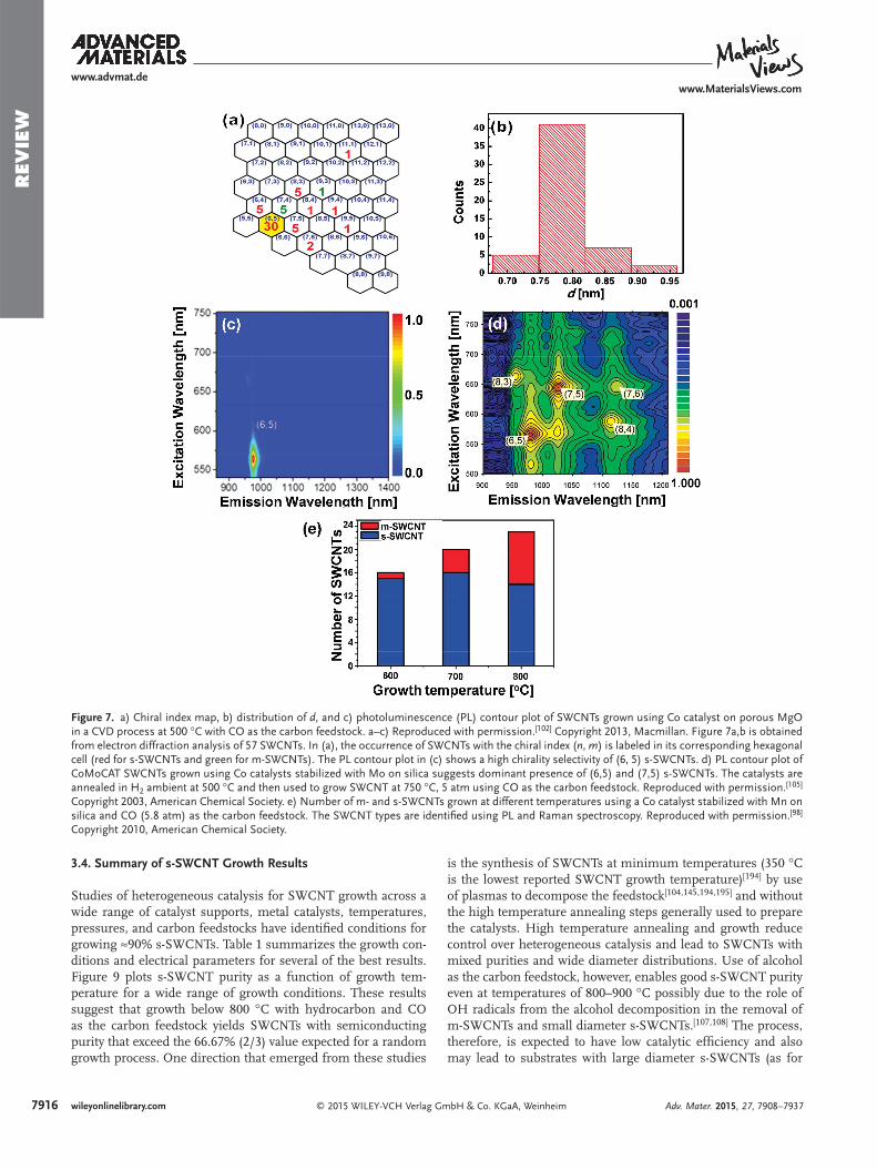
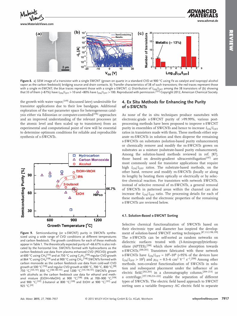
As discussed in the last section, carbon feedstocks such as hydrocarbons and CO cannot yield a high purity of s-SWCNTs at growth temperatures of 800–900 °C. Recent studies, how-ever, suggest that s-SWCNT purity at these temperatures can be improved by using alcohol vapor as the feedstock. Alcohol vapor was primarily introduced to reduce the growth temper-ature (which was above 1000 °C at that time) relative to that needed for other carbon feedstocks and also to minimize the formation of amorphous carbon and soot. [ 192 ] Subsequent studies suggested that high s-SWCNTs purity can result from growth either with alcohols having larger molecules such as isopropyl alcohol (IPA) [ 107,109 ] and 2-butanol, [ 109 ] or with a mix-ture of alcohols having smaller molecules such as an ethanol–methanol mixture. Use of IPA, in particular, can yield ≈87% s-SWCNT even at ≈900 °C, [ 107 ] as confi rmed using electrical measurements on transistors built using individual, isolated SWCNTs where 33 out of 38 transistors exhibited I ON / I OFF > 10 ( Figure 8 ). This purity is signifi cantly higher than the ≈64–67% s-SWCNTs and I ON / I OFF ≈ 2–5 obtained using eth-anol. [ 22,34,60,107 ] Similar electrical measurements for SWCNTs, which are grown using 2-butanol and an ethanol–methanol mixture ( Figure 9 ), [ 108 ] show ≈70–95% s-SWCNT purity. A mass spectroscopy analysis at the outlet of the CVD reactor suggests higher water to hydrocarbon ratios for the growth with IPA compared to ethanol, thereby clarifi ed the origin of improved purity. [ 107 ] In support of this observation, a con-trolled level of water exposure during growth induces selective etching of m-SWCNTs, [ 147,149,193 ] thereby increasing the yield of s-SWCNTs. Additional details on this in situ water-assisted etching of m-SWCNTs appear in Section 4.4.
Adv. Mater. 2015, 27, 7908–7937
www.advmat.dewww.MaterialsViews.com
7916 wileyonlinelibrary.com © 2015 WILEY-VCH Verlag GmbH & Co. KGaA, Weinheim
REV
IEW
3.4. Summary of s-SWCNT Growth Results
Studies of heterogeneous catalysis for SWCNT growth across a wide range of catalyst supports, metal catalysts, temperatures, pressures, and carbon feedstocks have identifi ed conditions for growing ≈90% s-SWCNTs. Table 1 summarizes the growth con-ditions and electrical parameters for several of the best results. Figure 9 plots s-SWCNT purity as a function of growth tem-perature for a wide range of growth conditions. These results suggest that growth below 800 °C with hydrocarbon and CO as the carbon feedstock yields SWCNTs with semiconducting purity that exceed the 66.67% (2/3) value expected for a random growth process. One direction that emerged from these studies
is the synthesis of SWCNTs at minimum temperatures (350 °C is the lowest reported SWCNT growth temperature) [ 194 ] by use of plasmas to decompose the feedstock [ 104,145,194,195 ] and without the high temperature annealing steps generally used to prepare the catalysts. High temperature annealing and growth reduce control over heterogeneous catalysis and lead to SWCNTs with mixed purities and wide diameter distributions. Use of alcohol as the carbon feedstock, however, enables good s-SWCNT purity even at temperatures of 800–900 °C possibly due to the role of OH radicals from the alcohol decomposition in the removal of m-SWCNTs and small diameter s-SWCNTs. [ 107,108 ] The process, therefore, is expected to have low catalytic effi ciency and also may lead to substrates with large diameter s-SWCNTs (as for
Adv. Mater. 2015, 27, 7908–7937
www.advmat.dewww.MaterialsViews.com
Figure 7. a) Chiral index map, b) distribution of d , and c) photoluminescence (PL) contour plot of SWCNTs grown using Co catalyst on porous MgO in a CVD process at 500 °C with CO as the carbon feedstock. a–c) Reproduced with permission. [ 102 ] Copyright 2013, Macmillan. Figure 7 a,b is obtained from electron diffraction analysis of 57 SWCNTs. In (a), the occurrence of SWCNTs with the chiral index ( n , m ) is labeled in its corresponding hexagonal cell (red for s-SWCNTs and green for m-SWCNTs). The PL contour plot in (c) shows a high chirality selectivity of (6, 5) s-SWCNTs. d) PL contour plot of CoMoCAT SWCNTs grown using Co catalysts stabilized with Mo on silica suggests dominant presence of (6,5) and (7,5) s-SWCNTs. The catalysts are annealed in H 2 ambient at 500 °C and then used to grow SWCNT at 750 °C, 5 atm using CO as the carbon feedstock. Reproduced with permission. [ 105 ] Copyright 2003, American Chemical Society. e) Number of m- and s-SWCNTs grown at different temperatures using a Co catalyst stabilized with Mn on silica and CO (5.8 atm) as the carbon feedstock. The SWCNT types are identifi ed using PL and Raman spectroscopy. Reproduced with permission. [ 98 ] Copyright 2010, American Chemical Society.
7917wileyonlinelibrary.com© 2015 WILEY-VCH Verlag GmbH & Co. KGaA, Weinheim
REV
IEW
the growth with water vapor, [ 149 ] discussed later) undesirable for transistor applications due to their low bandgaps. Additional exploration of the vast parameter space for heterogeneous catal-ysis either via Edisonian or computer-controlled [ 196 ] approaches and an improved understanding of the relevant processes (at the atomic level and then scaled up to transistors) from an experimental and computational point of view will be essential to determine optimum conditions for reliable and reproducible synthesis of s-SWCNTs.
4. Ex Situ Methods for Enhancing the Purity of s-SWCNTs
As none of the in situ techniques produce nanotubes with electronic-grade s-SWCNT purity of >99.99%, various post-processing methods have been proposed to improve s-SWCNT purity in ensembles of SWCNTs and hence to increase I ON / I OFF ratios in transistors made with them. These methods either sep-arate m-SWCNTs in solution and then disperse the remaining s-SWCNTs on substrates (solution-based purity enhancement) or chemically remove and modify the m-SWCNTs grown on substrates as a mixture (substrate-based purity enhancement). Among the solution-based methods reviewed in ref. [ 87 ] , those based on density-gradient ultracentrifugation [ 197 ] are most commonly used for transistor applications that require high I ON / I OFF ratios. The substrate-based methods, on the other hand, remove and modify m-SWCNTs (locally or along its length) by heating them optically or electrically or by selec-tive chemical reaction. For transistors with network SWCNTs, instead of selective removal of m-SWCNTs, a general removal of SWCNTs in patterned areas within the channel can also increase the I ON / I OFF ratio. The processing details for each of these methods and the electronic properties of the remaining s-SWCNTs are reviewed below.
4.1. Solution-Based s-SWCNT Sorting
Selective chemical functionalization of SWCNTs based on their electronic type and diameter has inspired the develop-ment of solution-based SWCNT sorting techniques. [ 87,112,198,199 ] The s-SWCNTs can be self-sorted as random networks on dielectric surfaces treated with (3-Aminopropyl)triethoxy-silane (APTES), [ 200 ] which show selective absorption towards s-SWCNTs. [ 200,201 ] Transistors fabricated with these network s-SWCNTs have I ON / I OFF ≈ 10 0 –10 6 (≈95% of the devices have I ON / I OFF > 10 2 ) and µ FE ≈ 0.5–6 cm 2 V −1 s −1 . [ 200 ] Among other methods, non-covalent functionalization of SWCNTs in solu-tion and subsequent placement under the infl uence of an electric fi eld, [ 202,203 ] in a chromatography column, [ 204–213 ] or a centrifuge, [ 197,198,214–222 ] enable the separation of different types of SWCNTs. The electric fi eld based approach to SWCNT sorting uses a variable frequency AC electric fi eld to separate
Adv. Mater. 2015, 27, 7908–7937
www.advmat.dewww.MaterialsViews.com
Figure 8. a) SEM image of a transistor with a single SWCNT (grown on quartz in a standard CVD at 900 °C using Fe as catalyst and isopropyl alcohol vapor as the carbon feedstock) bridging source and drain contacts. b) Transfer characteristics of 38 of such transistors; the red traces represent those with a single m-SWCNT; the blue traces represent those with a single s-SWCNT. c) Distribution of I ON / I OFF among the 38 transistors of (b) showing that 33 of them (≈87%) have I ON / I OFF > 10 and ≈80% have I ON / I OFF > 100. Reproduced with permission. [ 107 ] Copyright 2012, American Chemical Society.
Figure 9. Semiconducting (or s-SWCNT) purity in SWCNTs synthe-sized using a wide range of CVD conditions at different temperatures and carbon feedstock. The growth conditions for each of these methods appear in Table 1 . The theoretically expected purity of ≈66.67% is also indi-cated by the horizontal line. SWCNTs formed with hydrocarbons as the carbon feedstock use data from plasma enhanced CVD (PECVD) growth at 600 °C using CH 4 [ 145 ] and at 750 °C using C 2 H 2 , [ 104 ] regular CVD growth at 864 °C using CH 4 [ 109 ] and at 900 °C using CH 4 . [ 148 ] SWCNTs formed with carbon monoxide as the carbon feedstock use data from cold-wall CVD growth at 500 °C [ 102 ] and regular CVD growth at 600 °C, 700 °C, 800 °C, [ 98 ] 750 °C, [ 105,191 ] 850 °C, [ 188,189,191 ] and 1200 °C. [ 145,190,191 ] SWCNTs grown with alcohols as the carbon feedstock use data for ethanol and meth-anol mixture (EtOH+MeOH) at 900 °C, [ 108 ] IPA at 700–900 °C, [ 109 ] and 900 °C, [ 107 ] 2-butanol at 800 °C, [ 109 ] and EtOH at 900 °C, [ 107 ] and 925 °C. [ 22 ]
7918 wileyonlinelibrary.com © 2015 WILEY-VCH Verlag GmbH & Co. KGaA, Weinheim
REV
IEW m-SWCNTs in solution. [ 202,203 ] The high dielectric constants of
the m-SWCNTs compared to that of the solvent, which either can be sodium dodecyl sulfate (SDS) or sodium dodecyl benzene sulfonate (SDBS), ensure a positive dielectrophoretic force for the m-SWCNTs and align them between the electrodes used to apply the electric fi eld. The s-SWCNTs, along with some m-SWCNTs, remain in solution with unknown purity. Many attempts have been made to improve the s-SWCNT purity using dielectrophoretic sorting. [ 87,111 ] However, none has resulted in transistor demonstrations. (In spite of its ineffective-ness in SWCNT sorting, dielectrophoresis is routinely used to align sorted s-SWCNTs from solution placed in between two electrodes. [ 223–225 ] ) In the following, we discuss the chromatog-raphy- (Section 4.1.1) and centrifugation-(Section 4.1.2) based SWCNT sorting techniques. The transistor results using sorted SWCNTs obtained from these two methods are discussed sepa-rately in Section 4.1.3.
4.1.1. Chromatography
Two types of chromatography techniques have been used to sort SWCNTs. In ion-exchange chromatography (IEX), SWCNTs mixed in a DNA solution are injected into an exchange column containing anions that are thought to bind to the negatively charged phosphate groups of DNA. [ 207,208 ] The m-SWCNTs have carriers near the Fermi level and are easily polarized by these same phosphate groups. DNA-wrapped m-SWCNTs, therefore, have no net charge and only weakly interact with the anions in the exchange column. They exit the column with the fl ow of a low concentration NaSCN solution. By comparison, s-SWCNTs are diffi cult to polarize and hence, DNA-wrapped s-SWCNTs have an effective negative charge, enhanced attraction to the anions, and require a higher NaSCN concentration for their extraction from the column. Recent advances in the IEX tech-nique with optimizations of the DNA construct and the choice of anion yield SWNCT solutions with 60–90% purity and spe-cifi c chiral angles. [ 210 ] The implication of these purity improve-ments in transistor parameters is yet to be studied.
In gel chromatography, SWCNTs dispersed in aqueous solu-tions of SDS pass either through a single column [ 204–206,212,213 ] or through a series of columns [ 211 ] containing allyl dextran-based size-exclusion gel that interacts specifi cally with s-SWCNTs based on their diameter d . [ 211 ] As illustrated in Figure 10 a,b, the single column version inserts the m- and s-SWCNTs into the column and can only achieve SWCNT-type selectivity with up to 99.9% s-SWCNTs after three iterations [ 213 ] using a con-tinuous fl ow of SDS (and sometimes sodium cholate (SC) [ 212 ] ). The m-SWCNTs are fi rst eluted from the column, as they have less interaction with the gel, followed by the s-SWCNTs. The multi-column version, on the other hand, can achieve diameter-selectivity for the s-SWCNTs in addition to type-selectivity. The s-SWCNTs with smaller d have higher interaction with the gel and are collected in the upper column, while those with gradu-ally increasing d are collected downstream in the subsequent columns. The solution collected from the bottom-most column contains all m-SWCNTs and some s-SWCNTs (with d > 1.4 nm) that show no interaction with the gel, presumably because of complete SDS coatings.
4.1.2. Ultracentrifugation
The basic technique was pioneered by Svedberg in the 1920s and is now widely used in biology and life science. [ 227 ] In the past decade, ultracentrifugation has also been studied for sorting s-SWCNTs. [ 198,214–222,228 ] The choice of polymers such as poly(9,9-dioctylfl uorene) (PFO) and its compounds, poly(9,9-dioctylfl ourene- alt -(1,4-benzo-2,10,3-thiadiazole) (F8BT), regioregular poly(3-alkylthiophene) (rr-P3AT), regioregular poly(3-dodecylthiophene) (rr-P3DDT), poly(dithiafulvalene-fl u-orene- co - m -thiophene) (pDTGG-mT), etc. are critical for disper-sion of the s-SWCNTs in a manner that allows them to appear selectively as supernatant after ultracentrifugation. Raman analysis (radial breathing modes, RBMs) confi rms enrichment of s-SWCNTs in the supernatant (Figure 10 c,d).
In comparison with classical ultracentrifugation techniques, sorting of s- and m-SWCNTs is possible using density-gradient ultracentrifugation (DGU) [ 197 ] to yield s-SWCNT purity of up to ≈99.9%. [ 229 ] This technique disperses as-grown SWCNTs, obtained from CoMoCAT [ 188,230 ] or laser ablation [ 139 ] processes that synthesize SWCNTs with a few chiral indices, in solu-tions containing surfactants such as SC, SDS, or their com-binations. The dispersion unbundles the SWCNTs and encap-sulates them with surfactants. The dispersed SWCNTs are remixed with iodixanol and inserted at an isopycnic region (region with same density) using a syringe needle inside a den-sity gradient made with layers of iodixanol and SC mixtures at different concentrations (Figure 10 e). After ultracentrifu-gation, the surfactant-wrapped SWCNTs populate different regions of the centrifuge tube according to their buoyant den-sity. SWCNTs with smaller d, having a lower density, populate the upper part of the tube, while larger diameter SWCNTs and their bundles with higher density populate the lower part (Figure 10 f). With a suitable choice of starting SWCNT (CoMoCAT) and surfactants (a mixture of SC and SDS), it is possible to extract s- and m-SWCNTs from different regions of the centrifuge tube (Figure 10 g). The s-SWCNT purity after DGU varies from 90% to 99.9% depending on the number of successive iterations. [ 197,229 ]
4.1.3. Transistor Properties: Solution-Based Sorting
Gel Chromatography: Transistors containing high density, short (≈ µm) aligned s-SWCNTs (purity ≈99% after column chromatography) as the channel exhibit higher I ON / I OFF ratios for larger L CH / W ratios ( Figure 11 a,b), [ 27 ] consistent with the percolation theory. [ 27,34,184 ] For L CH ≈ 100 nm, only a few devices (10–20%) yield I ON / I OFF > 10 2 , as trace amounts of short, aligned m-SWCNTs (with purity ≈1%) bridge the source and drain contacts. This observation confi rms the need for >99.99% purity for high-performance electronics with L CH << 100 nm. The extracted values of µ FE ≈ 16–27 cm 2 V −1 s −1 for these transistors (Figure 11 b) suggest a small increase with decreasing L CH , as more s-SWCNTs directly bridge the source and drain contacts. These values of µ FE are comparable to those obtained for transistors with pristine SWCNT networks (Figure 6 f); however, the variation in the degree of alignment of the SWCNTs (i.e., higher alignment for transistors in
Adv. Mater. 2015, 27, 7908–7937
www.advmat.dewww.MaterialsViews.com
7919wileyonlinelibrary.com© 2015 WILEY-VCH Verlag GmbH & Co. KGaA, Weinheim
REV
IEW
Figure 11 b compared to those in Figure 6 f) prevent quantita-tive conclusions.
Transistors containing single s-SWCNT as the channel with L CH ≈ 100 nm using SWCNTs obtained from single-column multiple-cycle gel chromatography exhibit µ FE ≈ 20 cm 2 V −1 s −1 (average values, with a maximum of ≈80 cm 2 V −1 s −1 ). [ 213 ] Similar measurements on different sets of transistors with L CH ≈ 200 nm yield µ FE ≈ 40–150 cm 2 V −1 s −1 . [ 231 ] In
comparison, transistors that use pristine, as-grown s-SWCNTs and similar L CH exhibit signifi cantly higher µ FE (Figure 6 e), thereby suggesting the potential for improving such solution-based approaches.
Ultracentrifugation: Transistors made with s-SWCNTs puri-fi ed by ultracentrifugation with purity ≈94–99% and then deposited in random networks as the channel exhibit a range of I ON / I OFF ≈ 10 1 –10 5 (Figure 11 c,d), depending on the purity,
Adv. Mater. 2015, 27, 7908–7937
www.advmat.dewww.MaterialsViews.com
Figure 10. Optical images of a column a) before and b) after gel chromatography using a continuous fl ow of aqueous 1% SDS solution. The s-SWCNTs move slowly in the column compared to the m-SWCNTs. After certain durations of SDS fl ow, two distinct bands appear at the top and bottom of the column in (b) that correspond to s- and m-SWCNTs, respectively. a,b) Reproduced with permission. [ 213 ] Copyright 2013, American Chemical Society. Radial breathing mode (RBM) Raman spectra taken using 633 nm excitation before (as-received) and after (supernatant) SWCNT sorting via ultra-centrifugation with c) rr-P3DDT and d) a PFO-compound [ 198,226 ] as the solvent. The spectrum obtained for the supernatant has no m-SWCNT signals. c) Reproduced with permission. [ 216 ] Copyright 2011, Macmillan. d) Reproduced with permission. [ 198 ] Copyright 2014, American Chemical Society. e) Schematic illustration of SWCNT placement before density-gradient ultracentrifugation (DGU). A linear gradient of iodixanol is formed in between a dense underlayer and a buoyant overlayer. SWCNTs dispersed in surfactant solution are inserted inside the gradient at an isopycnic region. f) Optical image of SC-encapsulated CoMoCAT SWCNTs after DGU shows colored bands along the gradient. Nanotube bundles, aggregates, and insoluble mate-rial sediment form the lower part of the gradient, while SWCNTs of different d form the upper part of the gradient. The absorbance spectra on the right indicate SWCNTs with increasing d , having smaller bandgap and higher wavelength of absorption, are more concentrated at larger densities near the bottom of the gradient. SWCNTs with chiral indices (6,5), (7,5), and (9,5)/(8,7) are concentrated at different regions of the gradient. g) Optical image of laser ablation grown SWCNTs separated in a co-surfactant solution (1:4 SDS/SC). The top (orange) and bottom (green) band correspond to regions of highly enriched s-SWCNTs and m-SWCNTs, respectively. The absorbance spectra for these two bands are shown on the right. M11, S22, and S33 correspond to fi rst-order metallic, second-, and third-order semiconducting optical transitions (see Figure 21 ). e–g) Reproduced with permission. [ 197 ] Copyright 2006, Macmillan.
7920 wileyonlinelibrary.com © 2015 WILEY-VCH Verlag GmbH & Co. KGaA, Weinheim
REV
IEW
density, alignment, and length of the sorted s-SWCNTs and the device dimensions. [ 32,126,197,216,217,220,222,223 ] Following the percola-tion theory, [ 34,184 ] these transistors show higher I ON / I OFF ratios for larger purities and L CH / W ratios, and for smaller densities and W / L SWCNT ratios, where L SWCNT is the average length of
SWCNTs. The extracted values of µ FE for the sorted s-SWCNTs ranges from 1–50 cm 2 V −1 s −1 in transistors with L CH ≈ 1–100 µm (Figure 11 d,e), [ 81,216,217,220,222,223,228,232 ] even after SWCNT align-ment using dielectrophoresis [ 223 ] and self-assembly. [ 228 ] Though consideration of contact effects suggests intrinsic mobilities of
Figure 11. a) Transfer characteristics and b) calculated µ FE and I ON / I OFF ratios for transistors with a high density of chromatography-sorted, short-length (≈µm) aligned SWCNTs as the channel. The inset of (b) shows AFM image of the channel area. In (a), the transfer characteristics are plotted in a linear scale (left axis) for different L CH and in a logarithmic scale (right axis, blue dots) for L CH = 10 µm. a,b) Reproduced with permission. [ 27 ] Copyright 2013, Macmillan. c) Sheet conductance vs V GS characteristics of two transistors fabricated using networks of DGU-sorted s-SWCNT (red) and m-SWCNT (blue) as the channel. Insets show s-SWCNT characteristics in linear scale (bottom-left) and an representative AFM image of the SWCNT network used as the channel for transistors (top-right). The maximum slope of the linear scale plot allows calculation of µ FE ≈ 20 cm 2 V −1 s −1 . Reproduced with permission. [ 197 ] Copyright 2006, Macmillan. d) The variation in the I ON / I OFF ratio and µ FE (inset) with L CH for transistors made using DGU-sorted s-SWCNTs as the channel. Reproduced with permission. [ 32 ] Copyright 2012, American Chemical Society. e) Calculated µ FE and I ON / I OFF for transistors that use pDTFF-mT sorted SWCNT networks as the channel. Increase in SWCNT densities (with ≈94–96% s-SWCNTs) increases µ FE , but reduces the I ON / I OFF ratio. Reproduced with permission. [ 222 ] Copyright 2013, American Chemical Society.
Adv. Mater. 2015, 27, 7908–7937
www.advmat.dewww.MaterialsViews.com
7921wileyonlinelibrary.com© 2015 WILEY-VCH Verlag GmbH & Co. KGaA, Weinheim
REV
IEW
≈200–300 cm 2 V −1 s −1 for any L CH , [ 81 ] these values are signifi cantly lower than µ FE of >1000 cm 2 V −1 s −1 obtained in transistors with pristine SWCNTs as the channel (Figure 6 d,e).
Improvements in mobility and s-SWCNT purity remain the key focus for electronic applications of solution-based sorting methods. The presence of residual sur-factants and defects, [ 81,116 ] high resist-ance tube–tube junctions, [ 27,34 ] and short SWCNT lengths [ 27,233 ] are presumed ori-gins for low intrinsic mobilities in solution-sorted s-SWCNTs. Additional contributions from contact resistances will also require consideration.
4.2. Electrical Breakdown of m-SWCNTs
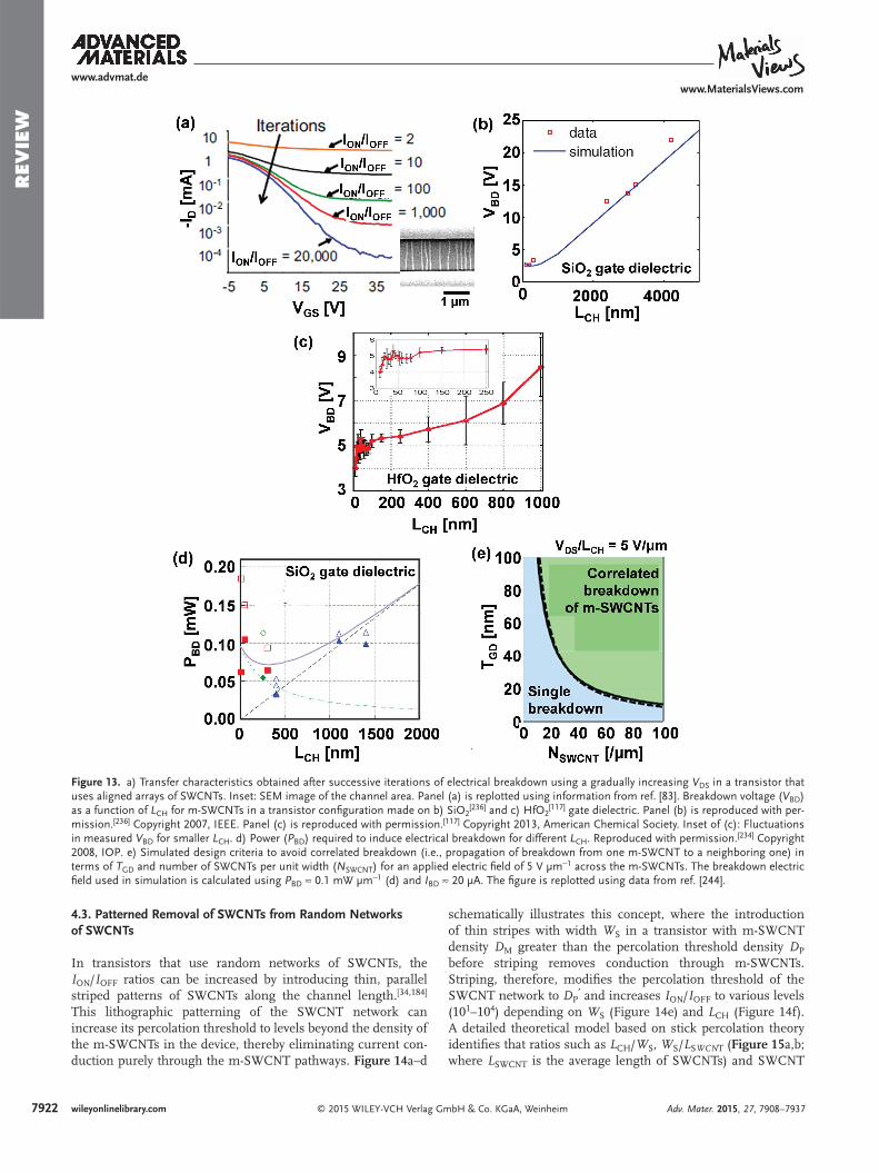
The fi rst demonstration of substrate-based m-SWCNT removal employed selec-tive electrical breakdown of m-SWCNTs using transistors with multiple SWCNTs as the channel. [ 115 ] During this process, the s-SWCNTs in a p-type transistor (that allows hole conduction) are electrostatically turned-off using positive V GS in a bottom-gated device geometry. An application of high V DS then induces Joule heating selectively in the m-SWCNTs and raises their temperatures signifi cantly. [ 234–240 ] Once the tem-perature reaches T BD (breakdown temperature) ≈600 °C, the m-SWCNTs are oxidized and are broken down near the center of the channel. [ 117,235,241 ] Heat dissipation into the contacts limits the temperature near source and drain [ 235,242 ] and does not allow breakdown in those regions. The application of elec-trical breakdown on transistors with both m- and s-SWCNTs ( Figure 12 a) increases the I ON / I OFF ratio from ≈10 1 to >10 3 (Figure 12 b,c).
Electrical breakdown cannot selectively remove m-SWCNTs in transistors with random networks of SWCNTs. For these transistors, heat conduction within neighboring SWCNTs raises their temperature and causes correlated breakdown of a set of m- and s-SWCNTs across the width of the transistor. [ 243 ] The process, however, is effective for transistors with aligned arrays of SWCNTs. For these transistors, electrical breakdown at a gradually increasing V DS causes corresponding increases in I ON / I OFF ( Figure 13 a), as the m-SWCNTs with higher con-ductivities are broken fi rst followed gradually by the ones with lower conductivities. [ 83 ] For these transistors (and also for transistors with a single m-SWCNT), the voltage V BD required to induce breakdown varies linearly with L CH for L CH > 1 µm. [ 117,234,236 ] In this regime, V BD = g ( T BD – T 0 ) L CH / I BD (Figure 13 b), where I BD is the breakdown current for a single m-SWCNT (≈20 µA [ 244 ] ), g is the thermal coupling coeffi cient for the m-SWCNT/dielectric interface and T 0 = 300 K. [ 236 ] For L CH < 1 µm, the “hot-phonon” effect reduces the current in the m-SWCNTs and increases V BD above the linear asymptote, [ 236 ] as observed in the measured V BD vs. L CH for transistors with different gate dielectrics (Figure 13 b,c). [ 117,234,236 ] Like V BD , the
power required to induce breakdown P BD also shows a non-linear trend for L CH < 1 µm. For L CH > 1 µm, P BD increases linearly at 0.1 mW µm −1 with an increase in L CH (Figure 13 d). One can explain the nonlinearity of the P BD variation with L CH for L CH < 1 µm by solving the heat equation for the m-SWCNTs after considering contributions from the thermal resistances at the m-SWCNT/source–drain contacts. [ 234 ] In transistors with high density of aligned arrays of SWCNTs as the channel and with T GD > 1/ N SWCNT , where N SWCNT is the number of SWCNTs per unit width of the transistor, a breakdown in one SWCNT can propagate to neighboring ones. [ 245,246 ] The use of T GD < 1/ N SWCNT avoids such correlated breakdown (Figure 13 e) [ 245 ] and enables the application of electrical break-down even with N SWCNT ≈ 100 µm −1 . [ 64 ]
The location and size (≈20–300 nm) of the breakdown for this m-SWCNT removal method varies randomly, [ 241,247 ] which limits the ability to defi ne device and circuits with source/drain contacts at predefi ned locations. [ 83,117 ] Along with this fundamental disadvantage, breakdown also requires SWCNT heating at powers of ≈0.1 mW µm −1 for L CH > 1 µm; this value increases for smaller L CH (Figure 13 d). Such high powers induce conduction in the s-SWCNTs with large d via band-to-band tunneling [ 119,248 ] and results in their removal via electrical breakdown. [ 83,249 ] Breakdown can also cause avalanche effects [ 250 ] and subsequent failure in gate dielectrics with signif-icant heat sinking at the contacts. [ 234 ] All these effects in com-bination degrade the performance of transistors fabricated with the remaining s-SWCNTs. The extracted µ FE is ≈350 cm 2 V −1 s −1 for L CH ≈ 1 µm transistors with low density SWCNTs, [ 83 ] whereas the value is ≈75 cm 2 V −1 s −1 for L CH ≈ 400 nm tran-sistors with high density SWCNTs, [ 64 ] both of which are lower than the pristine values (Figure 6 d,e).
Adv. Mater. 2015, 27, 7908–7937
www.advmat.dewww.MaterialsViews.com
Figure 12. a) SEM image of a transistor, in which a few SWCNTs bridge source and drain con-tacts. b) Conductance ( G D ≡ ∂ I D /∂ V DS ) modulation as a function of V GS in a transistor like the one in (a) before and after removal of m-SWCNTs from the channel using electrical breakdown. c) Plot of G ON / G OFF vs G ON before and after electrical breakdown for a set of transistors. Here, G ON ≡ G D @ V GS = –10 V and G OFF ≡ G D @ V GS = 10 V. Reproduced with permission. [ 115 ] Copyright 2001, American Association for the Advancement of Science (AAAS).
7922 wileyonlinelibrary.com © 2015 WILEY-VCH Verlag GmbH & Co. KGaA, Weinheim
REV
IEW
4.3. Patterned Removal of SWCNTs from Random Networks of SWCNTs
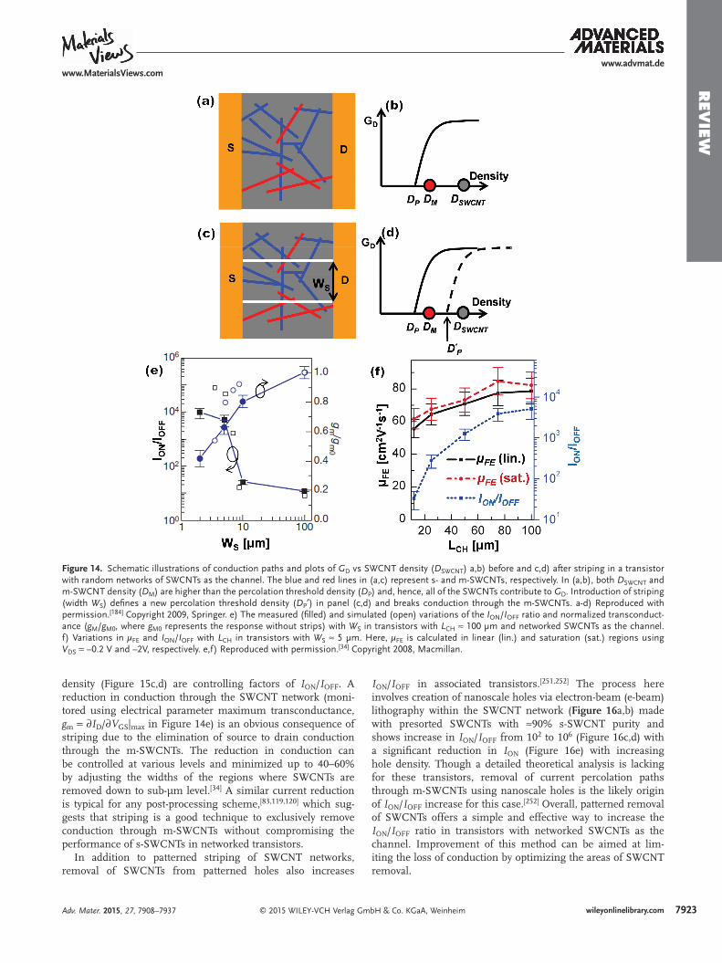
In transistors that use random networks of SWCNTs, the I ON / I OFF ratios can be increased by introducing thin, parallel striped patterns of SWCNTs along the channel length. [ 34,184 ] This lithographic patterning of the SWCNT network can increase its percolation threshold to levels beyond the density of the m-SWCNTs in the device, thereby eliminating current con-duction purely through the m-SWCNT pathways. Figure 14 a–d
schematically illustrates this concept, where the introduction of thin stripes with width W S in a transistor with m-SWCNT density D M greater than the percolation threshold density D P before striping removes conduction through m-SWCNTs. Striping, therefore, modifi es the percolation threshold of the SWCNT network to D P ′ and increases I ON / I OFF to various levels (10 1 –10 4 ) depending on W S (Figure 14 e) and L CH (Figure 14 f). A detailed theoretical model based on stick percolation theory identifi es that ratios such as L CH / W S , W S / L S WCN T ( Figure 15 a,b; where L SWCNT is the average length of SWCNTs) and SWCNT
Adv. Mater. 2015, 27, 7908–7937
www.advmat.dewww.MaterialsViews.com
Figure 13. a) Transfer characteristics obtained after successive iterations of electrical breakdown using a gradually increasing V DS in a transistor that uses aligned arrays of SWCNTs. Inset: SEM image of the channel area. Panel (a) is replotted using information from ref. [ 83 ] . Breakdown voltage ( V BD ) as a function of L CH for m-SWCNTs in a transistor confi guration made on b) SiO 2 [ 236 ] and c) HfO 2 [ 117 ] gate dielectric. Panel (b) is reproduced with per-mission. [ 236 ] Copyright 2007, IEEE. Panel (c) is reproduced with permission. [ 117 ] Copyright 2013, American Chemical Society. Inset of (c): Fluctuations in measured V BD for smaller L CH . d) Power ( P BD ) required to induce electrical breakdown for different L CH . Reproduced with permission. [ 234 ] Copyright 2008, IOP. e) Simulated design criteria to avoid correlated breakdown (i.e., propagation of breakdown from one m-SWCNT to a neighboring one) in terms of T GD and number of SWCNTs per unit width ( N SWCNT ) for an applied electric fi eld of 5 V µm −1 across the m-SWCNTs. The breakdown electric fi eld used in simulation is calculated using P BD ≈ 0.1 mW µm −1 (d) and I BD ≈ 20 µA. The fi gure is replotted using data from ref. [ 244 ] .
7923wileyonlinelibrary.com© 2015 WILEY-VCH Verlag GmbH & Co. KGaA, Weinheim
REV
IEW
density (Figure 15 c,d) are controlling factors of I ON / I OFF . A reduction in conduction through the SWCNT network (moni-tored using electrical parameter maximum transconductance, g m = ∂ I D /∂ V GS | max in Figure 14 e) is an obvious consequence of striping due to the elimination of source to drain conduction through the m-SWCNTs. The reduction in conduction can be controlled at various levels and minimized up to 40–60% by adjusting the widths of the regions where SWCNTs are removed down to sub-µm level. [ 34 ] A similar current reduction is typical for any post-processing scheme, [ 83,119,120 ] which sug-gests that striping is a good technique to exclusively remove conduction through m-SWCNTs without compromising the performance of s-SWCNTs in networked transistors.
In addition to patterned striping of SWCNT networks, removal of SWCNTs from patterned holes also increases
I ON / I OFF in associated transistors. [ 251,252 ] The process here involves creation of nanoscale holes via electron-beam (e-beam) lithography within the SWCNT network ( Figure 16 a,b) made with presorted SWCNTs with ≈90% s-SWCNT purity and shows increase in I ON / I OFF from 10 2 to 10 6 (Figure 16 c,d) with a signifi cant reduction in I ON (Figure 16 e) with increasing hole density. Though a detailed theoretical analysis is lacking for these transistors, removal of current percolation paths through m-SWCNTs using nanoscale holes is the likely origin of I ON / I OFF increase for this case. [ 252 ] Overall, patterned removal of SWCNTs offers a simple and effective way to increase the I ON / I OFF ratio in transistors with networked SWCNTs as the channel. Improvement of this method can be aimed at lim-iting the loss of conduction by optimizing the areas of SWCNT removal.
Adv. Mater. 2015, 27, 7908–7937
www.advmat.dewww.MaterialsViews.com
Figure 14. Schematic illustrations of conduction paths and plots of G D vs SWCNT density ( D SWCNT ) a,b) before and c,d) after striping in a transistor with random networks of SWCNTs as the channel. The blue and red lines in (a,c) represent s- and m-SWCNTs, respectively. In (a,b), both D SWCNT and m-SWCNT density ( D M ) are higher than the percolation threshold density ( D P ) and, hence, all of the SWCNTs contribute to G D . Introduction of striping (width W S ) defi nes a new percolation threshold density ( D P ′) in panel (c,d) and breaks conduction through the m-SWCNTs. a-d) Reproduced with permission. [ 184 ] Copyright 2009, Springer. e) The measured (fi lled) and simulated (open) variations of the I ON / I OFF ratio and normalized transconduct-ance ( g M / g M0 , where g M0 represents the response without strips) with W S in transistors with L CH ≈ 100 µm and networked SWCNTs as the channel. f) Variations in µ FE and I ON / I OFF with L CH in transistors with W S ≈ 5 µm. Here, µ FE is calculated in linear (lin.) and saturation (sat.) regions using V DS = –0.2 V and –2V, respectively. e,f) Reproduced with permission. [ 34 ] Copyright 2008, Macmillan.
7924 wileyonlinelibrary.com © 2015 WILEY-VCH Verlag GmbH & Co. KGaA, Weinheim
REV
IEW 4.4. Selective Chemical Modifi cation of m-SWCNTs
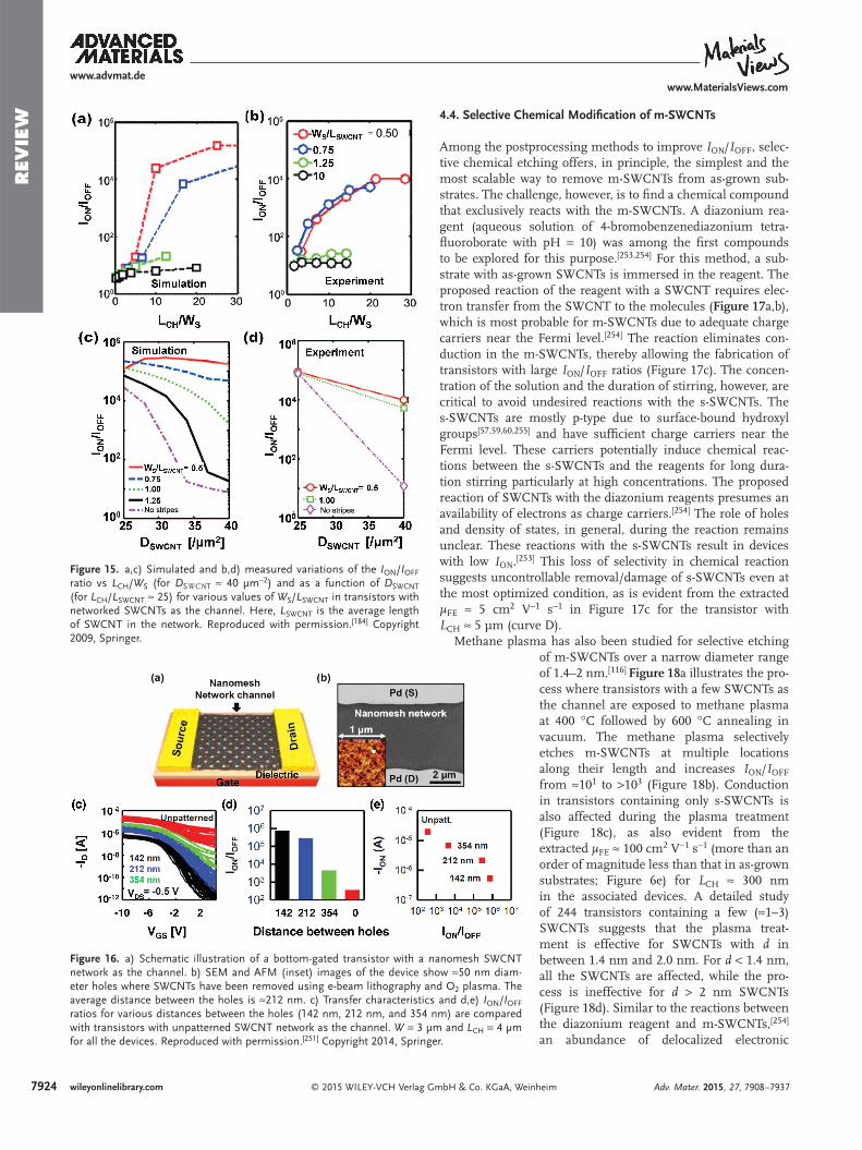
Among the postprocessing methods to improve I ON / I OFF , selec-tive chemical etching offers, in principle, the simplest and the most scalable way to remove m-SWCNTs from as-grown sub-strates. The challenge, however, is to fi nd a chemical compound that exclusively reacts with the m-SWCNTs. A diazonium rea-gent (aqueous solution of 4-bromobenzenediazonium tetra-fl uoroborate with pH = 10) was among the fi rst compounds to be explored for this purpose. [ 253,254 ] For this method, a sub-strate with as-grown SWCNTs is immersed in the reagent. The proposed reaction of the reagent with a SWCNT requires elec-tron transfer from the SWCNT to the molecules ( Figure 17 a,b), which is most probable for m-SWCNTs due to adequate charge carriers near the Fermi level. [ 254 ] The reaction eliminates con-duction in the m-SWCNTs, thereby allowing the fabrication of transistors with large I ON / I OFF ratios (Figure 17 c). The concen-tration of the solution and the duration of stirring, however, are critical to avoid undesired reactions with the s-SWCNTs. The s-SWCNTs are mostly p-type due to surface-bound hydroxyl groups [ 57,59,60,255 ] and have suffi cient charge carriers near the Fermi level. These carriers potentially induce chemical reac-tions between the s-SWCNTs and the reagents for long dura-tion stirring particularly at high concentrations. The proposed reaction of SWCNTs with the diazonium reagents presumes an availability of electrons as charge carriers. [ 254 ] The role of holes and density of states, in general, during the reaction remains unclear. These reactions with the s-SWCNTs result in devices with low I ON . [ 253 ] This loss of selectivity in chemical reaction suggests uncontrollable removal/damage of s-SWCNTs even at the most optimized condition, as is evident from the extracted µ FE ≈ 5 cm 2 V −1 s −1 in Figure 17 c for the transistor with L CH ≈ 5 µm (curve D).
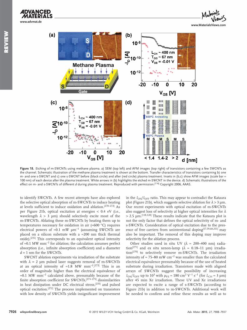
Methane plasma has also been studied for selective etching of m-SWCNTs over a narrow diameter range of 1.4–2 nm. [ 116 ] Figure 18 a illustrates the pro-cess where transistors with a few SWCNTs as the channel are exposed to methane plasma at 400 °C followed by 600 °C annealing in vacuum. The methane plasma selectively etches m-SWCNTs at multiple locations along their length and increases I ON / I OFF from ≈10 1 to >10 3 (Figure 18 b). Conduction in transistors containing only s-SWCNTs is also affected during the plasma treatment (Figure 18 c), as also evident from the extracted µ FE ≈ 100 cm 2 V −1 s −1 (more than an order of magnitude less than that in as-grown substrates; Figure 6 e) for L CH ≈ 300 nm in the associated devices. A detailed study of 244 transistors containing a few (≈1–3) SWCNTs suggests that the plasma treat-ment is effective for SWCNTs with d in between 1.4 nm and 2.0 nm. For d < 1.4 nm, all the SWCNTs are affected, while the pro-cess is ineffective for d > 2 nm SWCNTs (Figure 18 d). Similar to the reactions between the diazonium reagent and m-SWCNTs, [ 254 ] an abundance of delocalized electronic
Adv. Mater. 2015, 27, 7908–7937
www.advmat.dewww.MaterialsViews.com
Figure 15. a,c) Simulated and b,d) measured variations of the I ON / I OFF ratio vs L CH / W S (for D S WCN T ≈ 40 µm −2 ) and as a function of D SWCNT (for L CH / L SWCNT ≈ 25) for various values of W S / L SWCNT in transistors with networked SWCNTs as the channel. Here, L SWCNT is the average length of SWCNT in the network. Reproduced with permission. [ 184 ] Copyright 2009, Springer.
Figure 16. a) Schematic illustration of a bottom-gated transistor with a nanomesh SWCNT network as the channel. b) SEM and AFM (inset) images of the device show ≈50 nm diam-eter holes where SWCNTs have been removed using e-beam lithography and O 2 plasma. The average distance between the holes is ≈212 nm. c) Transfer characteristics and d,e) I ON / I OFF ratios for various distances between the holes (142 nm, 212 nm, and 354 nm) are compared with transistors with unpatterned SWCNT network as the channel. W = 3 µm and L CH = 4 µm for all the devices. Reproduced with permission. [ 251 ] Copyright 2014, Springer.
7925wileyonlinelibrary.com© 2015 WILEY-VCH Verlag GmbH & Co. KGaA, Weinheim
REV
IEW
states in the m-SWCNTs [ 256 ] explains their enhanced chemical reactivity with the methane plasma. The loss of selectivity for d < 1.4 nm SWCNTs apparently arises from the higher radius of curvature and higher strain in the C–C bond of SWCNTs that leads to enhanced chemical reactivity. [ 257,258 ] The absence of etching for d > 2 nm SWCNTs remains unexplained. In the future, the effectiveness of this approach will require a tighter diameter distribution (with d ≈ 1.4–2 nm) of the as-grown SWCNTs and a better selectivity for m-SWCNT etching without affecting the s-SWCNTs. In a recent paper, hydrogen is used as an in situ etchant for the m-SWCNTs. [ 259 ] The process yields ≈93% s-SWCNTs and I ON / I OFF > 10 4 , µ FE ≈ 10 cm 2 V −1 s −1 for L CH ≈ 100 µm transistors that use network SWCNTs as the channel. The extracted µ FE is an order of magnitude lower than the pristine values (Figure 6 f).
A few recent studies suggest the effectiveness of using oxidants such as water vapor to selectively etch m-SWCNTs from substrates with horizontally aligned SWCNTs. [ 147,149,193 ] Figure 19 shows an example of this approach on a substrate with a few s-SWCNTs (and 90% m-SWCNTs). The entire catalyst area (stripes at the top of Figure 19 a) and all m-SWCNTs are removed after ≈6000 ppm water treatment at 750 °C (Figure 19 c). Availability of electronic states near the Fermi level and a higher enthalpy change during the reaction of m-SWCNTs with hydroxyl groups explain this preferential etching. [ 108,193,260 ] A transistor made with water treated SWCNTs shows I ON / I OFF ≈ 3000 (Figure 19 e). The low I ON in this transistor might be due to the low concentration (≈10%) of s-SWCNTs on the pristine substrate and also due to the damage to some of the s-SWCNTs during water treatment. [ 193 ] In some cases, a trace amount of oxygen, a stronger oxidant than water, suggests
selective etching of m-SWCNTs. [ 261 ] In other cases, the catalyst support in the form of ceria, which contains active oxygen, enables growth of ≈95% s-SWCNTs, I ON / I OFF ≈ 15, and µ FE ≈ 1000 cm 2 V −1 s −1 for L CH ≈ 1 µm transistors that use arrays of SWCNTs as the channel. [ 106 ]
As opposed to ex situ removal of m-SWCNTs using water vapor at ≈6000 ppm, in situ etching of m-SWCNTs can occur at much lower water concentrations. [ 149 ] The effectiveness of this process requires SWCNT growth at a low rate, achieved by using a controlled fl ow of Ar through the ethanol bubbler, to ensure prolonged prox-imity of SWCNTs to catalysts and, hence, an enhanced possibility of m-SWCNT etching with the water vapor. [ 147,149,262–264 ] Transis-tors made with SWCNTs synthesized using ≈307 ppm water vapor show moderate I ON / I OFF = 10 1 –10 2 ( Figure 20 a–c). [ 149 ] One interesting feature of water-assisted growth is revealed at increased concentrations of the carbon feedstock; in this case, the increase in water concentration leads to increases in SWCNT density, along with an improved I ON / I OFF (Figure 20 d,e). Increase in water
concentration beyond an optimum value (≈508 ppm), however, etches all the SWCNTs with no selectivity, reduces the SWCNT density and the I ON / I OFF ratio (Figure 20 f). Even for the optimum water concentration of ≈508 ppm, SWCNTs with d < 1–1.5 nm are etched with no selectivity. [ 147,193 ] High local strain due to increased curvature in the small d SWCNTs explains such non-selective etching. [ 257,258 ] High local strain is also pre-sent in random SWCNTs near the catalyst area of aligned arrays of SWCNTs, [ 22,108,123,147 ] which inspired the use of multiple-cycle growth with intermittent water treatment in Ar ambient to remove random SWCNTs from the quartz substrate and increase the density of SWCNTs from 1–2 per µm to ≈10 per µm. [ 147 ] The diameter of SWCNTs grown in this manner, how-ever, increases after multiple cycles due to coarsening of catalyst sizes via Ostwald ripening. [ 147,154,156,157 ] Use of substrates, such as alumina, silica, or MgO that have higher catalytic activity to limit the sizes of the catalysts may become useful to avoid this coarsening. Overall, the applicability of chemical etching of m-SWCNTs with specifi c chemicals requires improvement in selectivity towards m-SWCNTs across broad ranges in diameter without affecting the s-SWCNTs.
4.5. Optical Excitation and Ablation of m-SWCNTs
Optical absorption in SWCNTs depends on the energy separa-tion between different Van Hove singularities in the density of states–energy diagrams of SWCNTs ( Figure 21 a). [ 265,266 ] The magnitude of this energy separation depends on the type and diameter of SWCNTs (Figure 21 b; Kataura plot), [ 265 ] a property that is routinely used in Raman spectroscopy [ 267 ] and PL [ 268,269 ]
Adv. Mater. 2015, 27, 7908–7937
www.advmat.dewww.MaterialsViews.com
Figure 17. a) Proposed reaction of diazonium reagents with a SWCNT. The reagents extract electrons from the SWCNT and form a stable C–C bond at its surface. The extent of electron transfer depends on the availability of charged carriers near the Fermi level and hence is more probable for m-SWCNTs. b) The functionalized SWCNT forms a radical cation and can fur-ther receive electrons from neighboring SWCNTs or react with fl uoride or diazonium salts. a,b) Replotted using information from ref. [ 254 ] . c) Transfer characteristics of a transistor (SEM image is shown at the top) before (A) and after diazonium reagent treatments (B–F). The curves (B,C) are after fi rst and second reactions with 5.3 × 10 −13 M solution, (D–F) are after third, fourth, and fi fth reactions with 3.7 × 10 −3 M solution, respectively. c) Reproduced with permission. [ 253 ] Copyright 2004, American Chemical Society.
7926 wileyonlinelibrary.com © 2015 WILEY-VCH Verlag GmbH & Co. KGaA, Weinheim
REV
IEW
to identify SWCNTs. A few recent attempts have also explored the selective optical absorption of m-SWCNTs to induce heating at levels suffi cient to induce oxidation and ablation. [ 270–272 ] As per Figure 21 b, optical excitation at energies < 0.4 eV (i.e., wavelength λ > 3 µm) should selectively excite most of the m-SWCNTs. Ablating these m-SWCNTs by heating them up to temperatures necessary for oxidation in air (≈600 °C) requires electrical powers of ≈0.1 mW µm −1 (assuming SWCNTs are placed on a silicon substrate with a ≈200 nm thick thermal oxide). [ 235 ] This corresponds to an equivalent optical intensity of ≈0.1 MW mm −2 for ablation; the calculation assumes perfect absorption (i.e., infi nite absorption coeffi cient) and a diameter d = 1 nm for the SWCNTs.
SWCNT ablation experiments via irradiation of the substrate with λ = 2 µm pulsed laser suggests removal of m-SWCNTs at an optical intensity of ≈1.8 MW mm −2 . [ 272 ] This is an order of magnitude higher than the electrical equivalence of ≈0.1 MW mm −2 calculated above, presumably because of the fi nite absorption coeffi cient for SWCNTs, [ 273–275 ] dissimilarities in heat dissipation under DC electrical stress, [ 235 ] and pulsed optical excitation. [ 272 ] The process implemented on transistors with low density of SWCNTs yields insignifi cant improvement
in the I ON / I OFF ratio. This may appear to contradict the Kataura plot (Figure 21 b), which suggests selective ablation for λ > 3 µm. Our recent experiments with optical excitation of m-SWCNTs also suggest loss of selectivity at higher optical intensities for λ > 2.5 µm. [ 118,120 ] These results indicate that the Kataura plot is not the only factor that defi nes the optical selectivity of m- and s-SWCNTs. Consideration of optical excitation due to the pres-ence of free carriers from unintentional doping [ 57,59,60,255 ] may also be important. The removal of this doping may improve selectivity for the ablation process.
Other studies used in situ UV ( λ ≈ 200–400 nm) radia-tion [ 271 ] and ex situ xenon-lamp ( λ ≈ 0.18–11 µm) irradia-tion [ 270 ] to selectively remove m-SWCNTs. The irradiation intensity of ≈ 75–80 mW cm −2 was smaller than the calculated electrical equivalence presumably because of the use of heated substrate during irradiation. Transistors made with aligned arrays of SWCNTs suggest the possibility of increasing I ON / I OFF up to 10 3 with µ FE ≈ 180 cm 2 V −1 s −1 (for L CH ≈ 3 µm) after 45 min Xe irradiation. These UV and Xe irradiations are expected to excite a range of s-SWCNTs (according to Figure 21 b) in addition to m-SWCNTs. Additional work will be needed to confi rm and refi ne these results as well as to
Adv. Mater. 2015, 27, 7908–7937
www.advmat.dewww.MaterialsViews.com
Figure 18. Etching of m-SWCNTs using methane plasma. a) SEM (top left) and AFM images (top right) of transistors containing a few SWCNTs as the channel. Schematic illustration of the methane plasma treatment is shown at the bottom. Transfer characteristics of transistors containing b) one m- and one s-SWCNT and c) one s-SWCNT before (black circle) and after (red circle) plasma treatment. Insets in (b,c) show AFM images (scale bar = 100 nm) of each device after the plasma treatment. White arrows in (b) highlights the etched m-SWCNT in the device. d) Schematic illustrations of the effect on m- and s-SWCNTs of different d during plasma treatment. Reproduced with permission. [ 116 ] Copyright 2006, AAAS.
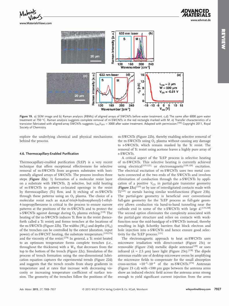
7927wileyonlinelibrary.com© 2015 WILEY-VCH Verlag GmbH & Co. KGaA, Weinheim
REV
IEW
explore the underlying chemical and physical mechanisms behind the process.
4.6. Thermocapillary-Enabled Purifi cation
Thermocapillary-enabled purifi cation (TcEP) is a very recent technique that offers exceptional effectiveness for selective removal of m-SWCNTs from as-grown substrates with hori-zontally aligned arrays of SWCNTs. The process involves three steps ( Figure 22 a): 1) formation of a molecular resist layer on a substrate with SWCNTs, 2) selective, but mild heating of m-SWCNTs to pattern co-located openings in the resist by thermocapillary (Tc) fl ow, and 3) etching of m-SWCNTs through these patterns using an O 2 plasma. The choice of a molecular resist such as α,α,α′-tris(4-hydroxyphenyl)-1-ethyl-4-isopropylbenzene is critical to the process to ensure narrow patterns at the positions of the m-SWCNTs and to protect the s-SWCNTs against damage during O 2 plasma etching. [ 119 ] The heating of the m-SWCNTs induces Tc fl ow in the resist (hence-forth called a Tc resist) and forms trenches at the locations of the m-SWCNTs (Figure 22 b). The widths ( W Tc ) and depths ( H Tc ) of the trenches can be controlled by the extent (duration, input power) of m-SWCNT heating, the substrate temperature, [ 119,276 ] and the viscosity of the resist. [ 276 ] In general, a Tc resist heated to an optimum temperature forms complete trenches (i.e., throughout the thickness) with a W Tc that decreases from the top to the bottom of the trench (Figure 22 c). Simulation of the process of trench formation using the one-dimensional lubri-cation equation captures the experimental trends (Figure 22 d) and suggests that the trench results from sharp gradients in temperature and at rates that increase with decreasing vis-cosity or increasing temperature coeffi cient of surface ten-sion. The geometry of the trenches follow the positions of the
m-SWCNTs (Figure 22 b), thereby enabling selective removal of the m-SWCNTs using O 2 plasma without causing any damage to s-SWCNTs, which remain masked by the Tc resist. The removal of Tc resist using acetone leaves a highly pure array of s-SWCNTs.
A critical aspect of the TcEP process is selective heating of m-SWCNTs. This selective heating is currently achieved using electrical [ 119,121 ] or electromagnetic [ 118,120 ] excitation. The electrical excitation of m-SWCNTs uses two metal con-tacts connected at the two ends of the SWCNTs and involves elimination of conduction through the s-SWCNTs by appli-cation of a positive V GS in partial-gate transistor geometry ( Figure 23 a) [ 119 ] or by use of interdigitated contacts made with Ti [ 121 ] or metals having similar workfunctions (Figure 23 b). The partial-gate geometry is benefi cial over conventional full-gate geometry for the TcEP process as full-gate geom-etry allows conduction via band-to-band tunneling near the cathode end in some of the s-SWCNTs with large d . [ 119,248 ] The second option eliminates the complexity associated with the partial-gate structure and relies on contacts with work-function near the mid-bandgap of s-SWCNTs instead, thereby resulting in high Schottky barriers that block electron and hole injection into s-SWCNTs and hence ensure good selec-tivity for the TcEP process. [ 121 ]
The electromagnetic approach to heat m-SWCNTs uses microwave irradiation with direct-contact (Figure 23 c) or removable (Figure 23 d) metallic dipole antennas [ 120 ] or uses infrared ( λ = 2.5 µm) laser light (Figure 23 e). [ 118 ] The dipole antennas enable use of desktop microwave ovens by amplifying the microwave fi elds to compensate for the small absorption cross-section ≈10 −5 –10 −4 of the m-SWCNTs. [ 274 ] Antennas (Figure 23 c,d) with <100 µm gaps between the antenna arms show an induced electric fi eld across the antenna arms strong enough to yield signifi cant current injection from the arms
Adv. Mater. 2015, 27, 7908–7937
www.advmat.dewww.MaterialsViews.com
Figure 19. a) SEM image and b) Raman analysis (RBMs) of aligned arrays of SWCNTs before water treatment. c,d) The same after 6000 ppm water treatment at 750 °C. Raman analysis suggests complete removal of m-SWCNTs in the red rectangle marked with M. e) Transfer characteristics of a transistor fabricated with aligned-array SWCNTs suggests I ON / I OFF ≈ 3000 after water treatment. Adapted with permission. [ 193 ] Copyright 2011, Royal Society of Chemistry.
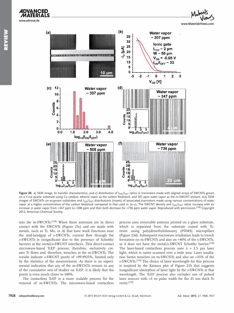
7928 wileyonlinelibrary.com © 2015 WILEY-VCH Verlag GmbH & Co. KGaA, Weinheim
REV
IEW
into the m-SWCNTs. [ 120 ] When these antennas are in direct contact with the SWCNTs (Figure 23 c) and are made with metals, such as Ti, Mo, or Al that have work functions near the mid-bandgap of s-SWCNTs, current fl ow through the s-SWCNTs is insignifi cant due to the presence of Schottky barriers at the metal/s-SWCNT interfaces. This direct-contact microwave-based TcEP process, therefore, exclusively cre-ates Tc fl ows and, therefore, trenches at the m-SWCNTs. The results indicate s-SWCNT purity of >99.9925%, limited only by the statistics of the measurement. As there is no experi-mental indication that any of the m-SWCNTs remain in any of the cumulative sets of studies on TcEP, it is likely that the purity is even much closer to 100%.
The contactless TcEP is a more scalable process for the removal of m-SWCNTs. The microwave-based contactless
process uses removable antenna printed on a glass substrate, which is separated from the substrate coated with Tc-resist using poly(dimethylsiloxane) (PDMS) micro pillars (Figure 23 d). Subsequent microwave irradiation leads to trench formation on m-SWCNTs and also on ≈40% of the s-SWCNTs, as it does not have the metal/s-SWCNT Schottky barrier. [ 120 ] The laser-based contactless process uses λ = 2.5 µm laser light, which is raster scanned over a wide area. Laser irradia-tion forms trenches on m-SWCNTs and also on ≈15% of the s-SWCNTs. [ 118 ] The choice of laser wavelength for this process is inspired by the Kataura plot of Figure 21 b that suggests insignifi cant absorption of laser light by the s-SWCNTs at that wavelength. The TcEP process also excludes use of pulsed laser sources with <5 ns pulse width for the 25 nm thick Tc resist. [ 118 ]
Adv. Mater. 2015, 27, 7908–7937
www.advmat.dewww.MaterialsViews.com
Figure 20. a) SEM image, b) transfer characteristics, and c) distribution of I ON / I OFF ratios in transistors made with aligned arrays of SWCNTs grown on a Y-cut quartz substrate using Cu catalyst, ethanol vapor as the carbon feedstock, and 307 ppm water vapor as the m-SWCNT etchant. d,e) SEM images of SWCNTs on as-grown substrates and I ON / I OFF distributions (insets) of associated transistors made using various concentrations of water vapor at a higher concentration of the carbon feedstock compared to that used in (a–c). The SWCNT density and I ON / I OFF ratios increase with an increase in water vapor from ≈347 ppm to ≈508 ppm and then both decrease for ≈736 ppm water vapor. Reproduced with permission. [ 149 ] Copyright 2012, American Chemical Society.
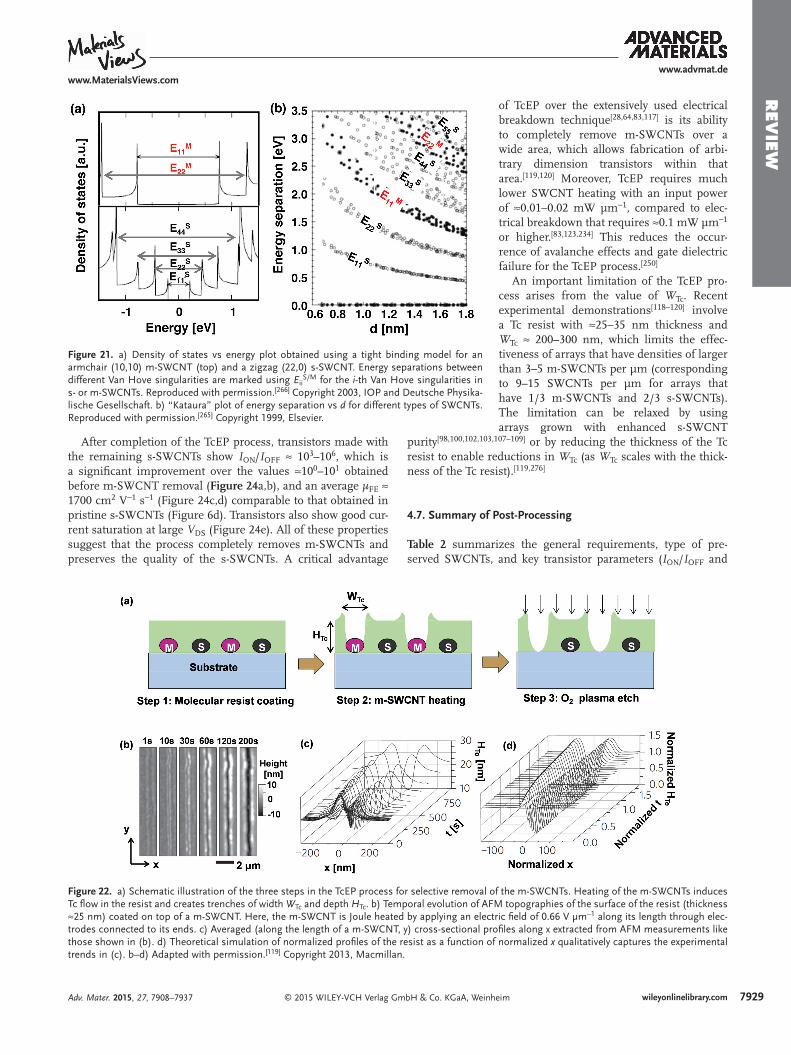
7929wileyonlinelibrary.com© 2015 WILEY-VCH Verlag GmbH & Co. KGaA, Weinheim
REV
IEW
Adv. Mater. 2015, 27, 7908–7937
www.advmat.dewww.MaterialsViews.com
After completion of the TcEP process, transistors made with the remaining s-SWCNTs show I ON / I OFF ≈ 10 3 –10 6 , which is a signifi cant improvement over the values ≈10 0 –10 1 obtained before m-SWCNT removal ( Figure 24 a,b), and an average µ FE ≈ 1700 cm 2 V −1 s −1 (Figure 24 c,d) comparable to that obtained in pristine s-SWCNTs (Figure 6 d). Transistors also show good cur-rent saturation at large V DS (Figure 24 e). All of these properties suggest that the process completely removes m-SWCNTs and preserves the quality of the s-SWCNTs. A critical advantage
of TcEP over the extensively used electrical breakdown technique [ 28,64,83,117 ] is its ability to completely remove m-SWCNTs over a wide area, which allows fabrication of arbi-trary dimension transistors within that area. [ 119,120 ] Moreover, TcEP requires much lower SWCNT heating with an input power of ≈0.01–0.02 mW µm −1 , compared to elec-trical breakdown that requires ≈0.1 mW µm −1 or higher. [ 83,123,234 ] This reduces the occur-rence of avalanche effects and gate dielectric failure for the TcEP process. [ 250 ]
An important limitation of the TcEP pro-cess arises from the value of W Tc . Recent experimental demonstrations [ 118–120 ] involve a Tc resist with ≈25–35 nm thickness and W Tc ≈ 200–300 nm, which limits the effec-tiveness of arrays that have densities of larger than 3–5 m-SWCNTs per µm (corresponding to 9–15 SWCNTs per µm for arrays that have 1/3 m-SWCNTs and 2/3 s-SWCNTs). The limitation can be relaxed by using arrays grown with enhanced s-SWCNT
purity [ 98,100,102,103,107–109 ] or by reducing the thickness of the Tc resist to enable reductions in W Tc (as W Tc scales with the thick-ness of the Tc resist). [ 119,276 ]
4.7. Summary of Post-Processing
Table 2 summarizes the general requirements, type of pre-served SWCNTs, and key transistor parameters ( I ON / I OFF and
Figure 22. a) Schematic illustration of the three steps in the TcEP process for selective removal of the m-SWCNTs. Heating of the m-SWCNTs induces Tc fl ow in the resist and creates trenches of width W Tc and depth H Tc . b) Temporal evolution of AFM topographies of the surface of the resist (thickness ≈25 nm) coated on top of a m-SWCNT. Here, the m-SWCNT is Joule heated by applying an electric fi eld of 0.66 V µm −1 along its length through elec-trodes connected to its ends. c) Averaged (along the length of a m-SWCNT, y) cross-sectional profi les along x extracted from AFM measurements like those shown in (b). d) Theoretical simulation of normalized profi les of the resist as a function of normalized x qualitatively captures the experimental trends in (c). b–d) Adapted with permission. [ 119 ] Copyright 2013, Macmillan.
Figure 21. a) Density of states vs energy plot obtained using a tight binding model for an armchair (10,10) m-SWCNT (top) and a zigzag (22,0) s-SWCNT. Energy separations between different Van Hove singularities are marked using E ii S/M for the i -th Van Hove singularities in s- or m-SWCNTs. Reproduced with permission. [ 266 ] Copyright 2003, IOP and Deutsche Physika-lische Gesellschaft. b) “Kataura” plot of energy separation vs d for different types of SWCNTs. Reproduced with permission. [ 265 ] Copyright 1999, Elsevier.
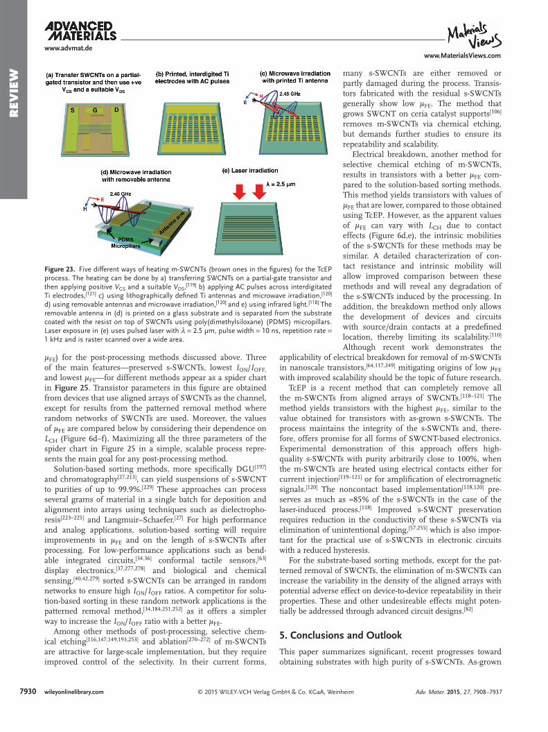
7930 wileyonlinelibrary.com © 2015 WILEY-VCH Verlag GmbH & Co. KGaA, Weinheim
REV
IEW
Adv. Mater. 2015, 27, 7908–7937
www.advmat.dewww.MaterialsViews.com
µ FE ) for the post-processing methods discussed above. Three of the main features—preserved s-SWCNTs, lowest I ON / I OFF, and lowest µ FE —for different methods appear as a spider chart in Figure 25 . Transistor parameters in this fi gure are obtained from devices that use aligned arrays of SWCNTs as the channel, except for results from the patterned removal method where random networks of SWCNTs are used. Moreover, the values of µ FE are compared below by considering their dependence on L CH (Figure 6 d–f). Maximizing all the three parameters of the spider chart in Figure 25 in a simple, scalable process repre-sents the main goal for any post-processing method.
Solution-based sorting methods, more specifi cally DGU [ 197 ] and chromatography [ 27,213 ] , can yield suspensions of s-SWCNT to purities of up to 99.9%. [ 229 ] These approaches can process several grams of material in a single batch for deposition and alignment into arrays using techniques such as dielectropho-resis [ 223–225 ] and Langmuir–Schaefer. [ 27 ] For high performance and analog applications, solution-based sorting will require improvements in µ FE and on the length of s-SWCNTs after processing. For low-performance applications such as bend-able integrated circuits, [ 34,36 ] conformal tactile sensors, [ 63 ] display electronics, [ 37,277,278 ] and biological and chemical sensing, [ 40,42,279 ] sorted s-SWCNTs can be arranged in random networks to ensure high I ON / I OFF ratios. A competitor for solu-tion-based sorting in these random network applications is the patterned removal method, [ 34,184,251,252 ] as it offers a simpler way to increase the I ON / I OFF ratio with a better µ FE .
Among other methods of post-processing, selective chem-ical etching [ 116,147,149,193,253 ] and ablation [ 270–272 ] of m-SWCNTs are attractive for large-scale implementation, but they require improved control of the selectivity. In their current forms,
many s-SWCNTs are either removed or partly damaged during the process. Transis-tors fabricated with the residual s-SWCNTs generally show low µ FE . The method that grows SWCNT on ceria catalyst supports [ 106 ] removes m-SWCNTs via chemical etching, but demands further studies to ensure its repeatability and scalability.
Electrical breakdown, another method for selective chemical etching of m-SWCNTs, results in transistors with a better µ FE com-pared to the solution-based sorting methods. This method yields transistors with values of µ FE that are lower, compared to those obtained using TcEP. However, as the apparent values of µ FE can vary with L CH due to contact effects (Figure 6 d,e), the intrinsic mobilities of the s-SWCNTs for these methods may be similar. A detailed characterization of con-tact resistance and intrinsic mobility will allow improved comparison between these methods and will reveal any degradation of the s-SWCNTs induced by the processing. In addition, the breakdown method only allows the development of devices and circuits with source/drain contacts at a predefi ned location, thereby limiting its scalability. [ 110 ] Although recent work demonstrates the
applicability of electrical breakdown for removal of m-SWCNTs in nanoscale transistors, [ 64,117,249 ] mitigating origins of low µ FE with improved scalability should be the topic of future research.
TcEP is a recent method that can completely remove all the m-SWCNTs from aligned arrays of SWCNTs. [ 118–121 ] The method yields transistors with the highest µ FE , similar to the value obtained for transistors with as-grown s-SWCNTs. The process maintains the integrity of the s-SWCNTs and, there-fore, offers promise for all forms of SWCNT-based electronics. Experimental demonstration of this approach offers high-quality s-SWCNTs with purity arbitrarily close to 100%, when the m-SWCNTs are heated using electrical contacts either for current injection [ 119–121 ] or for amplifi cation of electromagnetic signals. [ 120 ] The noncontact based implementation [ 118,120 ] pre-serves as much as ≈85% of the s-SWCNTs in the case of the laser-induced process. [ 118 ] Improved s-SWCNT preservation requires reduction in the conductivity of these s-SWCNTs via elimination of unintentional doping, [ 57,255 ] which is also impor-tant for the practical use of s-SWCNTs in electronic circuits with a reduced hysteresis.
For the substrate-based sorting methods, except for the pat-terned removal of SWCNTs, the elimination of m-SWCNTs can increase the variability in the density of the aligned arrays with potential adverse effect on device-to-device repeatability in their properties. These and other undesireable effects might poten-tially be addressed through advanced circuit designs. [ 82 ]
5. Conclusions and Outlook
This paper summarizes signifi cant, recent progresses toward obtaining substrates with high purity of s-SWCNTs. As-grown
Figure 23. Five different ways of heating m-SWCNTs (brown ones in the fi gures) for the TcEP process. The heating can be done by a) transferring SWCNTs on a partial-gate transistor and then applying positive V GS and a suitable V DS , [ 119 ] b) applying AC pulses across interdigitated Ti electrodes, [ 121 ] c) using lithographically defi ned Ti antennas and microwave irradiation, [ 120 ] d) using removable antennas and microwave irradiation, [ 120 ] and e) using infrared light. [ 118 ] The removable antenna in (d) is printed on a glass substrate and is separated from the substrate coated with the resist on top of SWCNTs using poly(dimethylsiloxane) (PDMS) micropillars. Laser exposure in (e) uses pulsed laser with λ = 2.5 µm, pulse width = 10 ns, repetition rate = 1 kHz and is raster scanned over a wide area.
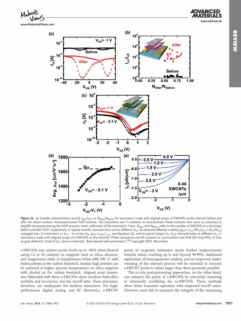
7931wileyonlinelibrary.com© 2015 WILEY-VCH Verlag GmbH & Co. KGaA, Weinheim
REV
IEW
Adv. Mater. 2015, 27, 7908–7937
www.advmat.dewww.MaterialsViews.com
s-SWCNTs may achieve purity levels up to ≈96% when formed using Co or Fe catalysts on supports such as silica, alumina, and magnesium oxide at temperatures below 600–700 °C with hydrocarbons as the carbon feedstock. Similar high purities can be achieved at higher process temperatures on silica supports with alcohol as the carbon feedstock. Aligned array transis-tors fabricated with these s-SWCNTs show excellent fi eld-effect mobility and on-current, but low on/off ratio. These processes, therefore, are inadequate for modern transistors. For high-performance digital, analog, and RF electronics, s-SWCNT
purity in as-grown substrates needs further improvements towards values reaching up to and beyond 99.99%. Additional exploration of heterogeneous catalysis and an improved under-standing of the relevant process will be essential to increase s-SWCNT purity to values larger than those presently possible.
The ex situ post-processing approaches, on the other hand, can enhance the purity of s-SWCNTs by selectively removing or chemically modifying the m-SWCNTs. These methods allow better transistor operation with improved on/off ratios. However, most fail to maintain the integrity of the remaining
Figure 24. a) Transfer characteristics and b) I ON / I OFF vs N After / N Before for transistors made with aligned arrays of SWCNTs as the channel before and after the direct contact, microwave-based TcEP process. The transistors use Ti contacts as source/drain; these contacts also serve as antennas to amplify microwave during the TcEP process; Inset: schematic of the transistors. Here, N After and N Before refer to the number of SWCNTs in a transistor before and after TcEP, respectively. c) Typical transfer characteristics at two different V DS , d) extracted effective mobility ( µ eff ≡ L CH / WC G V DS × ∂ I D /∂ V GS ) averaged over 12 transistors vs V GS – V T at low V DS ( µ FE ≡ µ eff | max , see Equation ( 2) , and e) typical output ( I D – V DS ) characteristics at different V GS in transistors made with aligned arrays of s-SWCNTs as the channel. These transistors use Pd contacts as source/drain and SU8 (50 nm)/HfO 2 (5 nm) as gate dielectric; Inset of (c): device schematic. Reproduced with permission. [ 120 ] Copyright 2014, Macmillan.
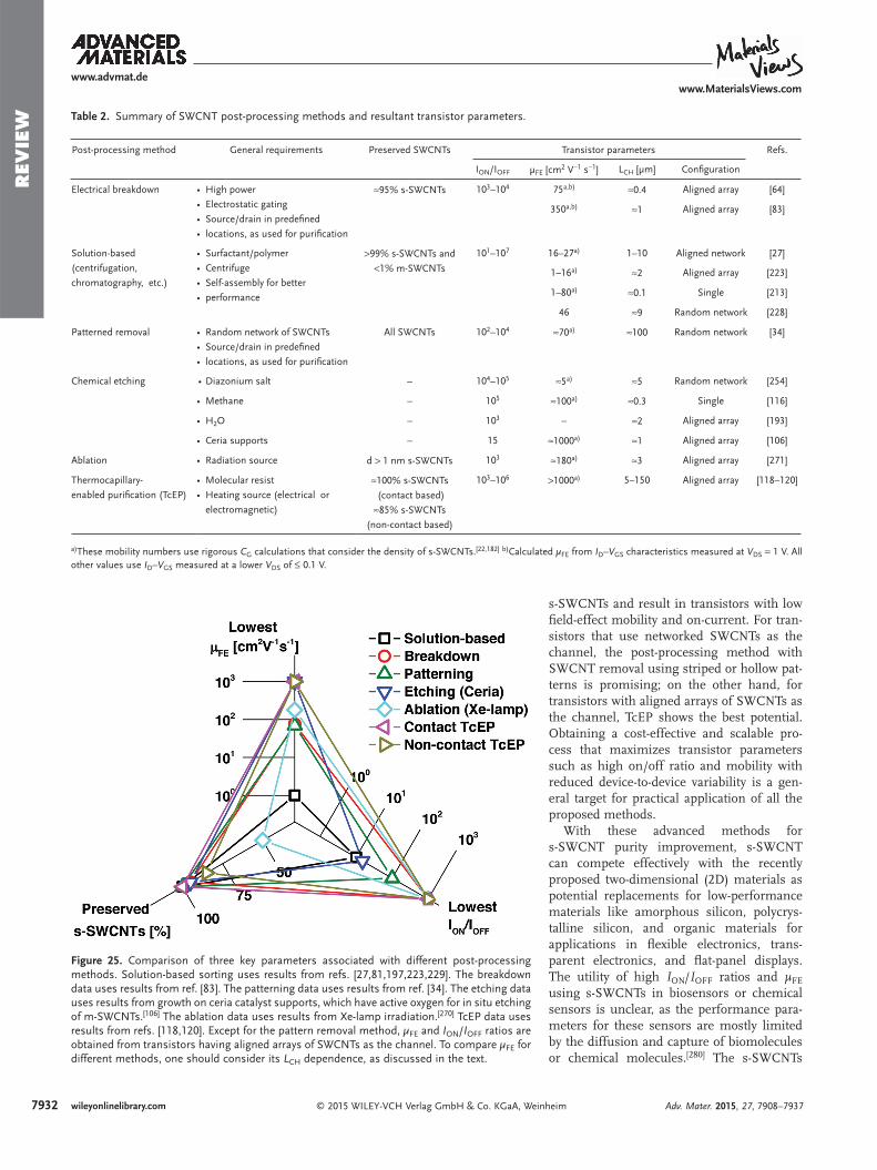
7932 wileyonlinelibrary.com © 2015 WILEY-VCH Verlag GmbH & Co. KGaA, Weinheim
REV
IEW Table 2. Summary of SWCNT post-processing methods and resultant transistor parameters.
Post-processing method General requirements Preserved SWCNTs Transistor parameters Refs.
I ON /I OFF µ FE [cm 2 V −1 s −1 ] L CH [µm] Confi guration
Electrical breakdown • High power
• Electrostatic gating
• Source/drain in predefi ned
• locations, as used for purifi cation
≈95% s-SWCNTs 10 3 –10 4 75 a,b) ≈0.4 Aligned array [64]
350 a,b) ≈1 Aligned array [83]
Solution-based
(centrifugation,
chromatography, etc.)
• Surfactant/polymer
• Centrifuge
• Self-assembly for better
• performance
>99% s-SWCNTs and
<1% m-SWCNTs
10 1 –10 7 16–27 a) 1–10 Aligned network [27]
1–16 a) ≈2 Aligned array [223]
1–80 a) ≈0.1 Single [213]
46 ≈9 Random network [228]
Patterned removal • Random network of SWCNTs
• Source/drain in predefi ned
• locations, as used for purifi cation
All SWCNTs 10 2 –10 4 ≈70 a) ≈100 Random network [34]
Chemical etching • Diazonium salt – 10 4 –10 5 ≈5 a) ≈5 Random network [254]
• Methane – 10 5 ≈100 a) ≈0.3 Single [116]
• H 2 O – 10 3 – ≈2 Aligned array [193 ]
• Ceria supports – 15 ≈1000 a) ≈1 Aligned array [106]
Ablation • Radiation source d > 1 nm s-SWCNTs 10 3 ≈180 a) ≈3 Aligned array [271]
Thermocapillary-
enabled purifi cation (TcEP)
• Molecular resist
• Heating source (electrical or
electromagnetic)
≈100% s-SWCNTs
(contact based)
≈85% s-SWCNTs
(non-contact based)
10 3 –10 6 >1000 a) 5–150 Aligned array [118–120]
a) These mobility numbers use rigorous C G calculations that consider the density of s-SWCNTs. [ 22,182 ] b) Calculated µ FE from I D – V GS characteristics measured at V DS = 1 V. All other values use I D – V GS measured at a lower V DS of ≤ 0.1 V.
Figure 25. Comparison of three key parameters associated with different post-processing methods. Solution-based sorting uses results from refs. [ 27,81,197,223,229 ] . The breakdown data uses results from ref. [ 83 ] . The patterning data uses results from ref. [ 34 ] . The etching data uses results from growth on ceria catalyst supports, which have active oxygen for in situ etching of m-SWCNTs. [ 106 ] The ablation data uses results from Xe-lamp irradiation. [ 270 ] TcEP data uses results from refs. [ 118,120 ] . Except for the pattern removal method, µ FE and I ON / I OFF ratios are obtained from transistors having aligned arrays of SWCNTs as the channel. To compare µ FE for different methods, one should consider its L CH dependence, as discussed in the text.
Adv. Mater. 2015, 27, 7908–7937
www.advmat.dewww.MaterialsViews.com
s-SWCNTs and result in transistors with low fi eld-effect mobility and on-current. For tran-sistors that use networked SWCNTs as the channel, the post-processing method with SWCNT removal using striped or hollow pat-terns is promising; on the other hand, for transistors with aligned arrays of SWCNTs as the channel, TcEP shows the best potential. Obtaining a cost-effective and scalable pro-cess that maximizes transistor parameters such as high on/off ratio and mobility with reduced device-to-device variability is a gen-eral target for practical application of all the proposed methods.
With these advanced methods for s-SWCNT purity improvement, s-SWCNT can compete effectively with the recently proposed two-dimensional (2D) materials as potential replacements for low-performance materials like amorphous silicon, polycrys-talline silicon, and organic materials for applications in fl exible electronics, trans-parent electronics, and fl at-panel displays. The utility of high I ON / I OFF ratios and µ FE using s-SWCNTs in biosensors or chemical sensors is unclear, as the performance para-meters for these sensors are mostly limited by the diffusion and capture of biomolecules or chemical molecules. [ 280 ] The s-SWCNTs
7933wileyonlinelibrary.com© 2015 WILEY-VCH Verlag GmbH & Co. KGaA, Weinheim
REV
IEW
Adv. Mater. 2015, 27, 7908–7937
www.advmat.dewww.MaterialsViews.com
have no dangling bonds, surface states and, in contrary to 2D materials, they have no grain boundaries, [ 281,282 ] which make them ideal for these applications. However, in addition to high purity s-SWCNTs, these applications will also demand pre-dictable and highly uniform transistor performance via pre-cise control of current conduction, threshold voltage, contact resistance, hysteresis, and sub-threshold (off-state to on-state) switching. All these outcomes can be ensured with s-SWCNTs that have a narrow diameter distribution, a suitable dopant, and a high density. The presented post-processing methods can achieve such diameter distribution, although at an expense of s-SWCNT density and, hence, will require the use of additional methods [ 27,64 ] for density improvement. To overcome use of any post-processing, the development of in situ methods with adequate control on heterogeneous catalysis is desirable, which will enable growth of s-SWCNTs with a narrow diameter dis-tribution at a high density. Successful further development of approaches to high purity s-SWCNTs with the added feature of controlled s-SWCNT doping offers the prospect to reignite the excitement for high-performance electronic applications of s-SWCNTs as a replacement of silicon.
Acknowledgements Financial support from National Research Council and Air Force Offi ce of Scientifi c Research are acknowledged for the preparation of this review article. A.E.I. also acknowledges discussions with Dr. Benji Maruyama, Dr. Rahul Rao, Dr. Pavel Nikolaev, Dr. Steve S. Kim, and Xu Xie.
Received: June 17, 2015 Revised: August 5, 2015
Published online: November 5, 2015
[1] S. Iijima , T. Ichihashi , Nature 1993 , 363 , 603 . [2] N. Behabtu , C. C. Young , D. E. Tsentalovich , O. Kleinerman ,
X. Wang , A. W. K. Ma , E. A. Bengio , R. F. ter Waarbeek , J. J. de Jong , R. E. Hoogerwerf , S. B. Fairchild , J. B. Ferguson , B. Maruyama , J. Kono , Y. Talmon , Y. Cohen , M. J. Otto , M. Pasquali , Science 2013 , 339 , 182 .
[3] X. Wang , N. Behabtu , C. C. Young , D. E. Tsentalovich , M. Pasquali , J. Kono , Adv. Funct. Mater. 2014 , 24 , 3241 .
[4] G. F. Close , S. Yasuda , B. Paul , S. Fujita , H. S. P. Wong , Nano Lett. 2008 , 8 , 706 .
[5] F. Kreupl , A. P. Graham , G. S. Duesberg , W. Steinhogl , M. Liebau , E. Unger , W. Honlein , Microelect. Eng. 2002 , 64 , 399 .
[6] H. Li , W.-Y. Yin , K. Banerjee , J.-F. Mao , IEEE Trans. Electron Devices 2008 , 55 , 1328 .
[7] A. Naeemi , R. Sarvari , J. D. Meindl , IEEE Electron Device Lett. 2005 , 26 , 84 .
[8] S. Esconjauregui , M. Fouquet , B. C. Bayer , C. Ducati , R. Smajda , S. Hofmann , J. Robertson , ACS Nano 2010 , 4 , 7431 .
[9] F. Kreupl , A. P. Graham , M. Liebau , G. S. Duesberg , R. Seidel , E. Unger , in IEEE Int. Electron. Devices Meet. , IEEE , Piscataway, NJ, USA 2004 , 683 .
[10] W. A. Deheer , A. Chatelain , D. Ugarte , Science 1995 , 270 , 1179 . [11] S. B. Fairchild , J. S. Bulmer , M. Sparkes , J. Boeckl , M. Cahay ,
T. Back , P. T. Murray , G. Gruen , M. Lange , N. P. Lockwood , F. Orozco , W. O’Neill , C. Paukner , K. K. K. Koziol , J. Mater. Res. 2014 , 29 , 392 .
[12] B. J. Landi , M. J. Ganter , C. D. Cress , R. A. DiLeo , R. P. Raffaelle , Energy Environ. Sci. 2009 , 2 , 638 .
[13] S. W. Lee , N. Yabuuchi , B. M. Gallant , S. Chen , B.-S. Kim , P. T. Hammond , Y. Shao-Horn , Nat. Nanotechnol. 2010 , 5 , 531 .
[14] A. L. M. Reddy , M. M. Shaijumon , S. R. Gowda , P. M. Ajayan , Nano Lett. 2009 , 9 , 1002 .
[15] R. S. Morris , B. G. Dixon , T. Gennett , R. Raffaelle , M. J. Heben , J. Power Sources 2004 , 138 , 277 .
[16] L. Dai , D. W. Chang , J.-B. Baek , W. Lu , Small 2012 , 8 , 1130 . [17] K. H. An , K. K. Jeon , J. K. Heo , S. C. Lim , D. J. Bae , Y. H. Lee , J.
Electrochem. Soc. 2002 , 149 , A1058 . [18] Y. Gogotsi , P. Simon , Science 2011 , 334 , 917 . [19] Q. Wang , Z. Wen , J. Li , Adv. Funct. Mater. 2006 , 16 , 2141 . [20] A. Javey , J. Guo , Q. Wang , M. Lundstrom , H. J. Dai , Nature 2003 ,
424 , 654 . [21] A. Javey , J. Guo , D. B. Farmer , Q. Wang , D. W. Wang , R. G. Gordon ,
M. Lundstrom , H. J. Dai , Nano Lett. 2004 , 4 , 447 . [22] S. J. Kang , C. Kocabas , T. Ozel , M. Shim , N. Pimparkar ,
M. A. Alam , S. V. Rotkin , J. A. Rogers , Nat. Nanotechnol. 2007 , 2 , 230 .
[23] J. Appenzeller , Proc. IEEE 2008 , 96 , 201 . [24] A. D. Franklin , Z. H. Chen , Nat. Nanotechnol. 2010 , 5 , 858 . [25] A. D. Franklin , S. O. Koswatta , D. B. Farmer , J. T. Smith , L. Gignac ,
C. M. Breslin , S.-J. Han , G. S. Tulevski , H. Miyazoe , W. Haensch , J. Tersoff , Nano Lett. 2013 , 13 , 2490 .
[26] A. D. Franklin , M. Luisier , S.-J. Han , G. Tulevski , C. M. Breslin , L. Gignac , M. S. Lundstrom , W. Haensch , Nano Lett. 2012 , 12 , 758 .
[27] Q. Cao , S.-j. Han , G. S. Tulevski , Y. Zhu , D. D. Lu , W. Haensch , Nat. Nanotechnol. 2013 , 8 , 180 .
[28] M. M. Shulaker , G. Hills , N. Patil , H. Wei , H.-Y. Chen , H. S. PhilipWong , S. Mitra , Nature 2013 , 501 , 526 .
[29] C. Kocabas , H.-S. Kim , T. Banks , J. A. Rogers , A. A. Pesetski , J. E. Baumgardner , S. V. Krishnaswamy , H. Zhang , Proc. Natl. Acad. Sci. USA 2008 , 105 , 1405 .
[30] K. Ryu , A. Badmaev , C. Wang , A. Lin , N. Patil , L. Gomez , A. Kumar , S. Mitra , H. S. P. Wong , C. W. Zhou , Nano Lett. 2009 , 9 , 189 .
[31] C. Rutherglen , D. Jain , P. Burke , Nat. Nanotechnol. 2009 , 4 , 811 . [32] C. Wang , J.-C. Chien , K. Takei , T. Takahashi , J. Nah , A. M. Niknejad ,
A. Javey , Nano Lett. 2012 , 12 , 1527 . [33] C. Kocabas , S. Dunham , Q. Cao , K. Cimino , X. N. Ho , H. S. Kim ,
D. Dawson , J. Payne , M. Stuenkel , H. Zhang , T. Banks , M. Feng , S. V. Rotkin , J. A. Rogers , Nano Lett. 2009 , 9 , 1937 .
[34] Q. Cao , H. S. Kim , N. Pimparkar , J. P. Kulkarni , C. J. Wang , M. Shim , K. Roy , M. A. Alam , J. A. Rogers , Nature 2008 , 454 , 495 .
[35] E. Artukovic , M. Kaempgen , D. S. Hecht , S. Roth , G. Gruner , Nano Lett. 2005 , 5 , 757 .
[36] D.-m. Sun , M. Y. Timmermans , Y. Tian , A. G. Nasibulin , E. I. Kauppinen , S. Kishimoto , T. Mizutani , Y. Ohno , Nat. Nano-technol. 2011 , 6 , 156 .
[37] P. Avouris , M. Freitag , V. Perebeinos , Nat. Photonics 2008 , 2 , 341 . [38] M. E. Itkis , A. P. Yu , R. C. Haddon , Nano Lett. 2008 , 8 , 2224 . [39] P. G. Collins , K. Bradley , M. Ishigami , A. Zettl , Science 2000 , 287 ,
1801 . [40] Q. F. Pengfei , O. Vermesh , M. Grecu , A. Javey , O. Wang , H. J. Dai ,
S. Peng , K. J. Cho , Nano Lett. 2003 , 3 , 347 . [41] J. Wang , Electroanalysis 2005 , 17 , 7 . [42] J. A. Robinson , E. S. Snow , S. C. Badescu , T. L. Reinecke ,
F. K. Perkins , Nano Lett. 2006 , 6 , 1747 . [43] M.-H. Ham , G. L. C. Paulus , C. Y. Lee , C. Song , K. Kalantar-zadeh ,
W. Choi , J.-H. Han , M. S. Strano , ACS Nano 2010 , 4 , 6251 . [44] G.-r. Li , F. Wang , Q.-w. Jiang , X.-p. Gao , P.-w. Shen , Angew. Chem.
Int. Ed. 2010 , 49 , 3653 . [45] M. W. Rowell , M. A. Topinka , M. D. McGehee , H.-J. Prall ,
G. Dennler , N. S. Sariciftci , L. Hu , G. Gruner , Appl. Phys. Lett. 2006 , 88 , 233506 .
7934 wileyonlinelibrary.com © 2015 WILEY-VCH Verlag GmbH & Co. KGaA, Weinheim
REV
IEW
Adv. Mater. 2015, 27, 7908–7937
www.advmat.dewww.MaterialsViews.com
[46] R. C. Tenent , T. M. Barnes , J. D. Bergeson , A. J. Ferguson , B. To , L. M. Gedvilas , M. J. Heben , J. L. Blackburn , Adv. Mater. 2009 , 21 , 3210 .
[47] Y. Ye , D. J. Bindl , R. M. Jacobberger , M.-Y. Wu , S. S. Roy , M. S. Arnold , Small 2014 , 10 , 3299 .
[48] X. J. Zhou , J. Y. Park , S. M. Huang , J. Liu , P. L. McEuen , Phys. Rev. Lett. 2005 , 95 , 146805 .
[49] T. Durkop , S. A. Getty , E. Cobas , M. S. Fuhrer , Nano Lett. 2004 , 4 , 35 .
[50] W. Kim , A. Javey , R. Tu , J. Cao , Q. Wang , H. J. Dai , Appl. Phys. Lett. 2005 , 87 , 173101 .
[51] Y. C. Tseng , K. Phoa , D. Carlton , J. Bokor , Nano Lett. 2006 , 6 , 1364 .
[52] Z. H. Chen , J. Appenzeller , J. Knoch , Y. M. Lin , P. Avouris , Nano Lett. 2005 , 5 , 1497 .
[53] Y. Nosho , Y. Ohno , S. Kishimoto , T. Mizutani , Appl. Phys. Lett. 2005 , 86 , 073105 .
[54] S. Wang , Q. S. Zeng , L. J. Yang , Z. Y. Zhang , Z. X. Wang , T. A. Pei , L. Ding , X. L. Liang , M. Gao , Y. Li , L. M. Peng , Nano Lett. 2011 , 11 , 23 .
[55] D. Shahrjerdi , A. D. Franklin , S. Oida , J. A. Ott , G. S. Tulevski , W. Haensch , ACS Nano 2013 , 7 , 8303 .
[56] H. Wei , H.-Y. Chen , L. Liyanage , H. S. P. Wong , S. Mitra , in IEEE Int. Electron Devices Meet. , IEEE , Piscataway, NJ, USA 2011 , p. 23.2.1 .
[57] W. Kim , A. Javey , O. Vermesh , O. Wang , Y. M. Li , H. J. Dai , Nano Lett. 2003 , 3 , 193 .
[58] S. A. McGill , S. G. Rao , P. Manandhar , P. Xiong , S. Hong , Appl. Phys. Lett. 2006 , 89 , 163123 .
[59] C. M. Aguirre , P. L. Levesque , M. Paillet , F. Lapointe , B. C. St-Antoine , P. Desjardins , R. Martel , Adv. Mater. 2009 , 21 , 3087 .
[60] S. H. Jin , A. E. Islam , T.-i. Kim , J.-h. Kim , M. A. Alam , J. A. Rogers , Adv. Funct. Mater. 2012 , 22 , 2276 .
[61] S. Park , M. Vosguerichian , Z. Bao , Nanoscale 2013 , 5 , 1727 . [62] J. Zhang , C. Wang , C. Zhou , ACS Nano 2012 , 6 , 7412 . [63] T. Takahashi , K. Takei , A. G. Gillies , R. S. Fearing , A. Javey , Nano
Lett. 2011 , 11 , 5408 . [64] M. M. Shulaker , G. Pitner , G. Hills , M. Giachino , H.-S. P. Wong ,
S. Mitra , in IEEE Int. Electron Devices Meet. , IEEE , Piscataway, NJ, USA 2014 , 812 .
[65] S. W. Hong , T. Banks , J. A. Rogers , Adv. Mater. 2010 , 22 , 1826 . [66] P. Hu , C. Zhang , A. Fasoli , V. Scardaci , S. Pisana , T. Hasan ,
J. Robertson , W. I. Milne , A. C. Ferrari , Phys. E (Amsterdam, Neth.) 2008 , 40 , 2278 .
[67] S. H. Hur , M. H. Yoon , A. Gaur , M. Shim , A. Facchetti , T. J. Marks , J. A. Rogers , J. Am. Chem. Soc. 2005 , 127 , 13808 .
[68] R. T. Weitz , U. Zschieschang , F. Effenberger , H. Klauk , M. Burghard , K. Kern , Nano Lett. 2007 , 7 , 22 .
[69] M. Terrones , P. M. Ajayan , F. Banhart , X. Blase , D. L. Carroll , J. C. Charlier , R. Czerw , B. Foley , N. Grobert , R. Kamalakaran , P. Kohler-Redlich , M. Ruhle , T. Seeger , H. Terrones , Appl. Phys. A: Mater. Sci. Process. 2002 , 74 , 355 .
[70] J. C. Charlier , M. Terrones , M. Baxendale , V. Meunier , T. Zacharia , N. L. Rupesinghe , W. K. Hsu , N. Grobert , H. Terrones , G. A. J. Amaratunga , Nano Lett. 2002 , 2 , 1191 .
[71] D. Golberg , Y. Bando , L. Bourgeois , K. Kurashima , T. Sato , Carbon 2000 , 38 , 2017 .
[72] K. Gong , F. Du , Z. Xia , M. Durstock , L. Dai , Science 2009 , 323 , 760 .
[73] A. Jorio , G. Dresselhaus , M. S. Dresselhaus , M. Terrones , A. G. S. Filho , A. M. Rao , in Carbon Nanotubes , Vol. 111 , Springer-Verlag , Berlin/Heidelberg, Germany 2008 , 531 .
[74] J. Campos-Delgado , I. O. Maciel , D. A. Cullen , D. J. Smith , A. Jorio , M. A. Pimenta , H. Terrones , M. Terrones , ACS Nano 2010 , 4 , 1696 .
[75] H. Wang , P. Wei , Y. Li , J. Han , H. R. Lee , B. D. Naab , N. Liu , C. Wang , E. Adijanto , B. C. K. Tee , S. Morishita , Q. Li , Y. Gao , Y. Cui , Z. Bao , Proc. Natl. Acad. Sci. USA 2014 , 111 , 4776 .
[76] B. C. Paul , S. Fujita , M. Okajima , T. H. Lee , H. S. P. Wong , Y. Nishi , IEEE Trans. Electron Devices 2007 , 54 , 2369 .
[77] H. S. P. Wong , S. Mitra , D. Akinwande , C. Beasley , Y. Chai , H.-Y. Chen , X. Chen , G. Close , J. Deng , A. Hazeghi , J. Liang , A. Lin , L. S. Liyanage , J. Luo , J. Parker , N. Patil , M. Shulaker , H. Wei , L. Wei , J. Zhang , in IEEE Int. Electron. Devices Meet. 2011 , p. 23.1.1 .
[78] A. Balijepalli , S. Sinha , Y. Cao , in IEEE Int. Symp. Low Power Elec-tron. Design 2007 , p. 2 .
[79] A. E. Islam , F. Du , X. Ho , S. H. Jin , S. Dunham , J. A. Rogers , J. Appl. Phys. 2012 , 111 , 054511 .
[80] A. D. Franklin , G. S. Tulevski , S.-J. Han , D. Shahrjerdi , Q. Cao , H.-Y. Chen , H. S. P. Wong , W. Haensch , ACS Nano 2012 , 6 , 1109 .
[81] Q. Cao , S.-J. Han , G. S. Tulevski , A. D. Franklin , W. Haensch , ACS Nano 2012 , 6 , 6471 .
[82] J. Zhang , N. P. Patil , A. Hazeghi , H. S. P. Wong , S. Mitra , IEEE Trans. Computer-Aided Design Integr. Circuits Syst. 2011 , 30 , 1103 .
[83] N. Patil , A. Lin , J. Zhang , H. Wei , K. Anderson , H. S. P. Wong , S. Mitra , in IEEE Int. Electron. Devices Meet. 2009 , p. 535 .
[84] A. D. Franklin , Nature 2013 , 498 , 443 . [85] Q. Cao , J. A. Rogers , Adv. Mater. 2009 , 21 , 29 . [86] P. Avouris , Z. Chen , V. Perebeinos , Nat. Nanotechnol. 2007 , 2 , 605 . [87] M. C. Hersam , Nat. Nanotechnol. 2008 , 3 , 387 . [88] G. D. Nessim , Nanoscale 2010 , 2 , 1306 . [89] C. Wang , K. Takei , T. Takahashi , A. Javey , Chem. Soc. Rev. 2013 , 42 ,
2592 . [90] Y. Chen , J. Zhang , Acc. Chem. Res. 2014 , 47 , 2273 . [91] Q. Zhang , J.-Q. Huang , M.-Q. Zhao , W.-Z. Qian , F. Wei , ChemSus
Chem 2011 , 4 , 864 . [92] L.-M. Peng , Z. Zhang , S. Wang , Mater. Today 2014 , 17 , 433 . [93] M. F. L. De Volder , S. H. Tawfi ck , R. H. Baughman , A. J. Hart ,
Science 2013 , 339 , 535 . [94] M. S. Dresselhaus , P. Avouris , Carbon Nanotubes 2001 , 80 , 1 . [95] S. Datta , Quantum Transport: Atom to Transistor , Cambridge Uni-
versity Press , Cambridge, UK 2005 . [96] H. Wang , Y. Yuan , L. Wei , K. Goh , D. Yu , Y. Chen , Carbon 2015 , 81 ,
1 . [97] J. Liu , C. Wang , X. Tu , B. Liu , L. Chen , M. Zheng , C. Zhou , Nat.
Commun. 2012 , 3 , 1199 . [98] C. Z. Loebick , R. Podila , J. Reppert , J. Chudow , F. Ren , G. L. Haller ,
A. M. Rao , L. D. Pfefferle , J. Am. Chem. Soc. 2010 , 132 , 11125 . [99] M. He , A. I. Chernov , P. V. Fedotov , E. D. Obraztsova , J. Sainio ,
E. Rikkinen , H. Jiang , Z. Zhu , Y. Tian , E. I. Kauppinen , M. Niemelae , A. O. I. Krauset , J. Am. Chem. Soc. 2010 , 132 , 13994 .
[100] H. Wang , B. Wang , X.-Y. Quek , L. Wei , J. Zhao , L.-J. Li , M. B. Chan-Park , Y. Yang , Y. Chen , J. Am. Chem. Soc. 2010 , 132 , 16747 .
[101] F. Yang , X. Wang , D. Zhang , J. Yang , D. Luo , Z. Xu , J. Wei , J.-Q. Wang , Z. Xu , F. Peng , X. Li , R. Li , Y. Li , M. Li , X. Bai , F. Ding , Y. Li , Nature 2014 , 510 , 522 .
[102] M. He , H. Jiang , B. Liu , P. V. Fedotov , A. I. Chernov , E. D. Obraztsova , F. Cavalca , J. B. Wagner , T. W. Hansen , I. V. Anoshkin , E. A. Obraztsova , A. V. Belkin , E. Sairanen , A. G. Nasibulin , J. Lehtonen , E. I. Kauppinen , Sci. Rep. 2013 , 3 , 1460 .
[103] B. Wang , C. H. P. Poa , L. Wei , L.-J. Li , Y. Yang , Y. Chen , J. Am. Chem. Soc. 2007 , 129 , 9014 .
[104] L. Qu , F. Du , L. Dai , Nano Lett. 2008 , 8 , 2682 . [105] S. M. Bachilo , L. Balzano , J. E. Herrera , F. Pompeo , D. E. Resasco ,
R. B. Weisman , J. Am. Chem. Soc. 2003 , 125 , 11186 . [106] X. Qin , F. Peng , F. Yang , X. He , H. Huang , D. Luo , J. Yang ,
S. Wang , H. Liu , L. Peng , Y. Li , Nano Lett. 2014 , 14 , 512 .
7935wileyonlinelibrary.com© 2015 WILEY-VCH Verlag GmbH & Co. KGaA, Weinheim
REV
IEW
Adv. Mater. 2015, 27, 7908–7937
www.advmat.dewww.MaterialsViews.com
[107] Y. Che , C. Wang , J. Liu , B. Liu , X. Lin , J. Parker , C. Beasley , H. S. P. Wong , C. Zhou , ACS Nano 2012 , 6 , 7454 .
[108] L. Ding , A. Tselev , J. Wang , D. Yuan , H. Chu , T. P. McNicholas , Y. Li , J. Liu , Nano Lett. 2009 , 9 , 800 .
[109] J. Parker , C. Beasley , A. Lin , H.-Y. Chen , H. S. P. Wong , Carbon 2012 , 50 , 5093 .
[110] J. Liu , M. C. Hersam , MRS Bull. 2010 , 35 , 315 . [111] N. Komatsu , F. Wang , Materials 2010 , 3 , 3818 . [112] H. Zhang , B. Wu , W. Hu , Y. Liu , Chem. Soc. Rev. 2011 , 40 , 1324 . [113] G. S. Tulevski , A. D. Franklin , D. Frank , J. M. Lobez , Q. Cao ,
H. Park , A. Afzali , S.-J. Han , J. B. Hannon , W. Haensch , ACS Nano 2014 , 8 , 8730 .
[114] A. D. Franklin , in Emerging Nanoelectronic Devices , (Eds: A. Chen , J. Hutchby , V. Zhirnov , G. Bourianoff ), John Wiley & Sons Ltd , Chichester, UK 2014 , p. 315 .
[115] P. C. Collins , M. S. Arnold , P. Avouris , Science 2001 , 292 , 706 . [116] G. Zhang , P. Qi , X. Wang , Y. Lu , X. Li , R. Tu , S. Bangsaruntip ,
D. Mann , L. Zhang , H. Dai , Science 2006 , 314 , 974 . [117] M. M. Shulaker , J. Van Rethy , T. F. Wu , L. S. Liyanage , H. Wei , Z. Li ,
E. Pop , G. Gielen , H. S. P. Wong , S. Mitra , ACS Nano 2014 , 8 , 3434 .
[118] F. Du , J. R. Felts , X. Xie , J. Song , Y. Li , M. R. Rosenberger , A. E. Islam , S. H. Jin , S. N. Dunham , C. Zhang , W. L. Wilson , Y. Huang , W. P. King , J. A. Rogers , ACS Nano 2014 , 8 , 12641 .
[119] S. H. Jin , S. N. Dunham , J. Song , X. Xie , J.-H. Kim , C. Lu , A. Islam , F. Du , J. Kim , J. Felts , Y. Li , F. Xiong , M. A. Wahab , M. Menon , E. Cho , K. L. Grosse , D. J. Lee , H. U. Chung , E. Pop , M. A. Alam , W. P. King , Y. Huang , J. A. Rogers , Nat. Nanotechnol. 2013 , 8 , 347 .
[120] X. Xie , S. H. Jin , M. A. Wahab , A. E. Islam , C. Zhang , F. Du , E. Seabron , T. Lu , S. N. Dunham , H. I. Cheong , Y.-C. Tu , Z. Guo , H. U. Chung , Y. Li , Y. Liu , J.-H. Lee , J. Song , Y. Huang , M. A. Alam , W. L. Wilson , J. A. Rogers , Nat. Commun. 2014 , 5 , 5332 .
[121] X. Xie , M. Wahab , Y. Li , A. E. Islam , B. Tomic , J. Huang , B. Burns , E. Seabron , S. Dunham , F. Du , J. Lin , W. Wilson , J. Song , Y. Huang , M. Alam , J. A. Rogers , J. Appl. Phys. 2015 , 117 , 134303 .
[122] S. Natarajan , M. Agostinelli , S. Akbar , M. Bost , A. Bowonder , V. Chikarmane , S. Chouksey , A. Dasgupta , K. Fischer , Q. Fu , T. Ghani , M. Giles , S. Govindaraju , R. Grover , W. Han , D. Hanken , E. Haralson , M. Haran , M. Heckscher , R. Heussner , P. Jain , R. James , R. Jhaveri , I. Jin , H. Kam , E. Karl , C. Kenyon , M. Liu , Y. Luo , R. Mehandru , S. Morarka , L. Neiberg , P. Packan , A. Paliwal , C. Parker , P. Patel , R. Patel , C. Pelto , L. Pipes , P. Plekhanov , M. Prince , S. Rajamani , J. Sandford , B. Sell , S. Sivakumar , P. Smith , B. Song , K. Tone , T. Troeger , J. Wiedemer , M. Yang , K. Zhang , in IEEE Int. Electron Devices Meet. 2014 , 3.7.1 .
[123] N. Patil , A. Lin , E. R. Myers , K. Ryu , A. Badmaev , C. W. Zhou , H. S. P. Wong , S. Mitra , IEEE Trans. Nanotechnol. 2009 , 8 , 498 .
[124] D. K. Schroder , Semiconductor Material and Device Characteriza-tion , Wiley-IEEE Press , New Jersey 2006 .
[125] B. Razavi , Design of Analog CMOS Integrated Circuits , McGraw-Hill , New York 2000 .
[126] C. Wang , A. Badmaev , A. Jooyaie , M. Q. Bao , K. L. Wang , K. Galatsis , C. W. Zhou , ACS Nano 2011 , 5 , 4169 .
[127] F. Schwierz , J. J. Liou , Modern Microwave Transistors: Theory, Design, and Performance , Wiley-Interscience , New Jersey 2002 .
[128] F. Schwierz , Nat. Nanotechnol. 2010 , 5 , 487 . [129] F. Schwierz , Proc. IEEE 2013 , 101 , 1567 . [130] S. Lee , B. Koo , J. G. Park , H. Moon , J. Hahn , J. M. Kim , MRS Bull.
2006 , 31 , 455 . [131] P. van der Wilt , M. G. Kane , A. B. Limanov , A. H. Firester ,
L. Goodman , J. Lee , J. Abelson , A. M. Chitu , J. S. Im , MRS Bull. 2006 , 31 , 461 .
[132] W. S. Wong , A. Salleo , Flexible Electronics: Materials and Applica-tions , Springer US , New York 2009 .
[133] D. M. Wilson , S. Hoyt , J. Janata , K. Booksh , L. Obando , IEEE Sens. J. 2001 , 1 , 256 .
[134] Sensors: Chemical and Biochemical Sensors , (Eds: W. Göpel , T. A. Jones , M. Kleitz , I. Lundström , T. Seiyama ), Wiley-VCH , Wein-heim, Germany 2008 .
[135] A. Mason , S. C. Mukhopadhyay , K. P. Jayasundera , N. Bhattacharyya , Sensing Technology: Current Status and Future Trends I , Springer International Publishing , Switzerland 2014 .
[136] M. Joseyacaman , M. Mikiyoshida , L. Rendon , J. G. Santiesteban , Appl. Phys. Lett. 1993 , 62 , 202 .
[137] M. Kumar , Y. Ando , J. Nanosci. Nanotechnol. 2010 , 10 , 3739 . [138] S. Iijima , Nature 1991 , 354 , 56 . [139] A. Thess , R. Lee , P. Nikolaev , H. J. Dai , P. Petit , J. Robert , C. H. Xu ,
Y. H. Lee , S. G. Kim , A. G. Rinzler , D. T. Colbert , G. E. Scuseria , D. Tomanek , J. E. Fischer , R. E. Smalley , Science 1996 , 273 , 483 .
[140] M. J. Behr , E. A. Gaulding , K. A. Mkhoyan , E. S. Aydil , J. Appl. Phys. 2010 , 108 .
[141] F.-B. Rao , T. Li , Y.-L. Wang , Phys. E (Amsterdam, Neth.) 2008 , 40 , 779 .
[142] R. E. Smalley , Y. Li , V. C. Moore , B. K. Price , R. Colorado Jr. , H. K. Schmidt , R. H. Hauge , A. R. Barron , J. M. Tour , J. Am. Chem. Soc. 2006 , 128 , 15824 .
[143] Z. Ren , Nat. Nanotechnol. 2007 , 2 , 17 . [144] B. Liu , J. Liu , X. Tu , J. Zhang , M. Zheng , C. Zhou , Nano Lett. 2013 ,
13 , 4416 . [145] Y. M. Li , D. Mann , M. Rolandi , W. Kim , A. Ural , S. Hung , A. Javey ,
J. Cao , D. W. Wang , E. Yenilmez , Q. Wang , J. F. Gibbons , Y. Nishi , H. J. Dai , Nano Lett. 2004 , 4 , 317 .
[146] J. L. Xiao , S. Dunham , P. Liu , Y. W. Zhang , C. Kocabas , L. Moh , Y. G. Huang , K. C. Hwang , C. Lu , W. Huang , J. A. Rogers , Nano Lett. 2009 , 9 , 4311 .
[147] J. Li , K. Liu , S. Liang , W. Zhou , M. Pierce , F. Wang , L. Peng , J. Liu , ACS Nano 2014 , 8 , 554 .
[148] W. Kim , H. C. Choi , M. Shim , Y. M. Li , D. W. Wang , H. J. Dai , Nano Lett. 2002 , 2 , 703 .
[149] W. Zhou , S. Zhan , L. Ding , J. Liu , J. Am. Chem. Soc. 2012 , 134 , 14019 .
[150] Y. Li , J. Liu , Y. Q. Wang , Z. L. Wang , Chem. Mater. 2001 , 13 , 1008 . [151] Y. M. Li , W. Kim , Y. G. Zhang , M. Rolandi , D. W. Wang , H. J. Dai , J.
Phys. Chem. B 2001 , 105 , 11424 . [152] H. Ago , K. Nakamura , K. Ikeda , N. Uehara , N. Ishigami , M. Tsuji ,
Chem. Phys. Lett. 2005 , 408 , 433 . [153] P. B. Amama , C. L. Pint , S. M. Kim , L. McJilton , K. G. Eyink ,
E. A. Stach , R. H. Hauge , B. Maruyama , ACS Nano 2010 , 4 , 895 . [154] S. M. Kim , C. L. Pint , P. B. Amama , D. N. Zakharov , R. H. Hauge ,
B. Maruyama , E. A. Stach , J. Phys. Chem. Lett. 2010 , 1 , 918 . [155] E. F. Kukovitsky , S. G. L’Vov , N. A. Sainov , V. A. Shustov ,
L. A. Chernozatonskii , Chem. Phys. Lett. 2002 , 355 , 497 . [156] P. B. Amama , C. L. Pint , L. McJilton , S. M. Kim , E. A. Stach ,
P. T. Murray , R. H. Hauge , B. Maruyama , Nano Lett. 2009 , 9 , 44 .
[157] S. M. Kim , C. L. Pint , P. B. Amama , R. H. Hauge , B. Maruyama , E. A. Stach , J. Mater. Res. 2010 , 25 , 1875 .
[158] A. E. Islam , P. Nikolaev , P. B. Amama , S. Saber , D. Zakharov , D. Huffman , M. Erford , G. Sargent , S. L. Semiatin , E. A. Stach , B. Maruyama , Nano Lett. 2014 , 14 , 4997 .
[159] B. L. Liu , W. C. Ren , S. S. Li , C. Liu , H. M. Cheng , Chem. Commun. 2012 , 48 , 2409 .
[160] B. Kitiyanan , W. E. Alvarez , J. H. Harwell , D. E. Resasco , Chem. Phys. Lett. 2000 , 317 , 497 .
[161] D. B. Geohegan , A. A. Puretzky , I. N. Ivanov , S. Jesse , G. Eres , J. Y. Howe , Appl. Phys. Lett. 2003 , 83 , 1851 .
[162] T. Labbaye , A. Canizares , M. Gaillard , T. Lecas , E. Kovacevic , C. Boulmer-Leborgne , T. Strunskus , N. Raimboux , P. Simon , G. Guimbretiere , M. R. Ammar , Appl. Phys. Lett. 2014 , 105 , 213109 .
7936 wileyonlinelibrary.com © 2015 WILEY-VCH Verlag GmbH & Co. KGaA, Weinheim
REV
IEW
Adv. Mater. 2015, 27, 7908–7937
www.advmat.dewww.MaterialsViews.com
[163] M. Picher , E. Anglaret , R. Arenal , V. Jourdain , Nano Lett. 2009 , 9 , 542 .
[164] R. Rao , D. Liptak , T. Cherukuri , B. I. Yakobson , B. Maruyama , Nat. Mater. 2012 , 11 , 213 .
[165] A. A. Puretzky , D. B. Geohegan , S. Jesse , I. N. Ivanov , G. Eres , Appl. Phys. A: Mater. Sci. Process. 2005 , 81 , 223 .
[166] F. Ding , A. R. Harutyunyan , B. I. Yakobson , Proc. Natl. Acad. Sci. USA 2009 , 106 , 2506 .
[167] E. C. Neyts , A. C. T. van Duin , A. Bogaerts , J. Am. Chem. Soc. 2012 , 134 , 1256 .
[168] A. J. Page , K. R. S. Chandrakumar , S. Irle , K. Morokuma , J. Am. Chem. Soc. 2011 , 133 , 621 .
[169] Y. Shibuta , S. Maruyama , Chem. Phys. Lett. 2003 , 382 , 381 . [170] N. Latorre , E. Romeo , F. Cazana , T. Ubieto , C. Royo ,
J. J. Villacampa , A. Monzon , J. Phys. Chem. C 2010 , 114 , 4773 . [171] S. Naha , I. K. Puri , J. Phys. D: Appl. Phys. 2008 , 41 , 065304 . [172] S. Reich , L. Li , J. Robertson , Phys. Rev. B 2005 , 72 , 165423 . [173] S. Sawada , N. Hamada , Solid State Commun. 1992 , 83 , 917 . [174] J. R. Heath , Nature 1998 , 393 , 730 . [175] C. Kocabas , S.-H. Hur , A. Gaur , M. A. Meitl , M. Shim , J. A. Rogers ,
Small 2005 , 1 , 1110 . [176] S. Huang , X. Cai , J. Liu , J. Am. Chem. Soc. 2003 , 125 , 5636 . [177] A. Ismach , L. Segev , E. Wachtel , E. Joselevich , Angew. Chem. Int.
Ed. 2004 , 43 , 6140 . [178] S. Han , X. L. Liu , C. W. Zhou , J. Am. Chem. Soc. 2005 , 127 ,
5294 . [179] H. Ago , K. Imamoto , N. Ishigami , R. Ohdo , K.-i. Ikeda , M. Tsuji ,
Appl. Phys. Lett. 2007 , 90 , 123112 . [180] C. Kocabas , S. J. Kang , T. Ozel , M. Shim , J. A. Rogers , J. Phys.
Chem. C 2007 , 111 , 17879 . [181] Q. Cao , S. H. Hur , Z. T. Zhu , Y. G. Sun , C. J. Wang , M. A. Meitl ,
M. Shim , J. A. Rogers , Adv. Mater. 2006 , 18 , 304 . [182] Q. Cao , M. G. Xia , C. Kocabas , M. Shim , S. V. Rotkin , J. A. Rogers ,
Appl. Phys. Lett. 2007 , 90 , 023516 . [183] N. Pimparkar , M. A. Alam , IEEE Electron Device Lett. 2008 , 29 ,
1037 . [184] N. Pimparkar , Q. Cao , J. A. Rogers , M. A. Alam , Nano Res. 2009 ,
2 , 167 . [185] H. Hongo , F. Nihey , S. Yorozu , J. Appl. Phys. 2010 , 107 ,
094501 . [186] J. R. H. Ross , Heterogeneous Catalysis: Fundamentals and Applica-
tions , Elsevier , Amsterdam 2012 . [187] J. Robertson , J. Mater. Chem. 2012 , 22 , 19858 . [188] D. E. Resasco , W. E. Alvarez , F. Pompeo , L. Balzano , J. E. Herrera ,
B. Kitiyanan , A. Borgna , J. Nanopart. Res. 2002 , 4 , 131 . [189] G. Lolli , L. Zhang , L. Balzano , N. Sakulchaicharoen , Y. Tan ,
D. E. Resasco , J. Phys. Chem. B 2006 , 110 , 2108 . [190] P. Nikolaev , M. J. Bronikowski , R. K. Bradley , F. Rohmund ,
D. T. Colbert , K. A. Smith , R. E. Smalley , Chem. Phys. Lett. 1999 , 313 , 91 .
[191] A. V. Naumov , O. A. Kuznetsov , A. R. Harutyunyan , A. A. Green , M. C. Hersam , D. E. Resasco , P. N. Nikolaev , R. B. Weisman , Nano Lett. 2009 , 9 , 3203 .
[192] S. Maruyama , R. Kojima , Y. Miyauchi , S. Chiashi , M. Kohno , Chem. Phys. Lett. 2002 , 360 , 229 .
[193] P. Li , J. Zhang , J. Mater. Chem. 2011 , 21 , 11815 . [194] M. Cantoro , S. Hofmann , S. Pisana , V. Scardaci , A. Parvez ,
C. Ducati , A. C. Ferrari , A. M. Blackburn , K. Y. Wang , J. Robertson , Nano Lett. 2006 , 6 , 1107 .
[195] E. Mora , J. M. Pigos , F. Ding , B. I. Yakobson , A. R. Harutyunyan , J. Am. Chem. Soc. 2008 , 130 , 11840 .
[196] P. Nikolaev , D. Hooper , N. Perea-Lopez , M. Terrones , B. Maruyama , ACS Nano 2014 , 8 , 10214 .
[197] M. S. Arnold , A. A. Green , J. F. Hulvat , S. I. Stupp , M. C. Hersam , Nat. Nanotechnol. 2006 , 1 , 60 .
[198] S. K. Samanta , M. Fritsch , U. Scherf , W. Gomulya , S. Z. Bisri , M. A. Loi , Acc. Chem. Res. 2014 , 47 , 2446 .
[199] R. Martel , ACS Nano 2008 , 2 , 2195 . [200] M. C. LeMieux , M. Roberts , S. Barman , Y. W. Jin , J. M. Kim , Z. Bao ,
Science 2008 , 321 , 101 . [201] D. Chattopadhyay , L. Galeska , F. Papadimitrakopoulos , J. Am.
Chem. Soc. 2003 , 125 , 3370 . [202] R. Krupke , F. Hennrich , H. von Lohneysen , M. M. Kappes , Science
2003 , 301 , 344 . [203] R. Krupke , F. Hennrich , M. M. Kappes , H. V. Lohneysen , Nano
Lett. 2004 , 4 , 1395 . [204] S. Fujii , T. Tanaka , Y. Miyata , H. Suga , Y. Naitoh , T. Minari ,
T. Miyadera , K. Tsukagoshi , H. Kataura , Appl. Phys. Expr. 2009 , 2 , 071601 .
[205] T. Tanaka , H. Jin , Y. Miyata , S. Fujii , H. Suga , Y. Naitoh , T. Minari , T. Miyadera , K. Tsukagoshi , H. Kataura , Nano Lett. 2009 , 9 , 1497 .
[206] T. Tanaka , H. Jin , Y. Miyata , H. Kataura , Appl. Phys. Expr. 2008 , 1 , 114001 .
[207] M. Zheng , A. Jagota , E. D. Semke , B. A. Diner , R. S. McLean , S. R. Lustig , R. E. Richardson , N. G. Tassi , Nat. Mater. 2003 , 2 , 338 .
[208] M. Zheng , A. Jagota , M. S. Strano , A. P. Santos , P. Barone , S. G. Chou , B. A. Diner , M. S. Dresselhaus , R. S. McLean , G. B. Onoa , G. G. Samsonidze , E. D. Semke , M. Usrey , D. J. Walls , Science 2003 , 302 , 1545 .
[209] M. S. Strano , M. Zheng , A. Jagota , G. B. Onoa , D. A. Heller , P. W. Barone , M. L. Usrey , Nano Lett. 2004 , 4 , 543 .
[210] X. Tu , S. Manohar , A. Jagota , M. Zheng , Nature 2009 , 460 , 250 . [211] H. Liu , D. Nishide , T. Tanaka , H. Kataura , Nat. Commun. 2011 , 2 ,
309 . [212] K. Moshammer , F. Hennrich , M. M. Kappes , Nano Res. 2009 , 2 ,
599 . [213] G. S. Tulevski , A. D. Franklin , A. Afzali , ACS Nano 2013 , 7 , 2971 . [214] J. Han , Q. Ji , S. Qiu , H. Li , S. Zhang , H. Jin , Q. Li , Chem. Commun.
2015 , 51 , 4712 . [215] Y. Kato , M. Fukuzawa , F. Toshimitsu , N. Nakashima , Chem. Lett.
2015 , 44 , 566 . [216] H. W. Lee , Y. Yoon , S. Park , J. H. Oh , S. Hong , L. S. Liyanage ,
H. Wang , S. Morishita , N. Patil , Y. J. Park , J. J. Park , A. Spakowitz , G. Galli , F. Gygi , P. H. S. Wong , J. B. H. Tok , J. M. Kim , Z. Bao , Nat. Commun. 2011 , 2 , 541 .
[217] L. S. Liyanage , H. Lee , N. Patil , S. Park , S. Mitra , Z. Bao , H.-S. P. Wong , ACS Nano 2012 , 6 , 451 .
[218] S. Park , H. W. Lee , H. Wang , S. Selvarasah , M. R. Dokmeci , Y. J. Park , S. N. Cha , J. M. Kim , Z. Bao , ACS Nano 2012 , 6 , 2487 .
[219] S. D. Stranks , A. M. R. Baker , J. A. Alexander-Webber , B. Dirks , R. J. Nicholas , Small 2013 , 9 , 2245 .
[220] A. K. Sundramoorthy , S. Mesgari , J. Wang , R. Kumar , M. A. Sk , S. H. Yeap , Q. Zhang , S. K. Sze , K. H. Lim , M. B. Chan-Park , J. Am. Chem. Soc. 2013 , 135 , 5569 .
[221] F. Toshimitsu , N. Nakashima , Nat. Commun. 2014 , 5 , 5041 . [222] H. Wang , J. Mei , P. Liu , K. Schmidt , G. Jimenez-Oses , S. Osuna ,
L. Fang , C. J. Tassone , A. P. Zoombelt , A. N. Sokolov , K. N. Houk , M. F. Toney , Z. Bao , ACS Nano 2013 , 7 , 2659 .
[223] B. K. Sarker , S. Shekhar , S. I. Khondaker , ACS Nano 2011 , 5 , 6297 . [224] Q. Cao , S.-j. Han , G. S. Tulevski , Nat. Commun. 2014 , 5 , 5071 . [225] K. Yamamoto , S. Akita , Y. Nakayama , J. Phys. D: Appl. Phys. 1998 ,
31 , L34 . [226] H. Ozawa , N. Ide , T. Fujigaya , Y. Niidome , N. Nakashima , Chem.
Lett. 2011 , 40 , 239 . [227] K. E. Van Holde , J. C. Hansen , Biochem. Mol. Biol. 1998 , 11 , 933 . [228] G. J. Brady , Y. Joo , S. S. Roy , P. Gopalan , M. S. Arnold , Appl. Phys.
Lett. 2014 , 104 , 083107 . [229] NanoIntegris, Inc., http://www.nanointegris.com/en/semicon-
ducting (accessed: June, 2015).
7937wileyonlinelibrary.com© 2015 WILEY-VCH Verlag GmbH & Co. KGaA, Weinheim
REV
IEW
[230] Southwest NanoTechnologies, Inc., http://www.swentnano.com/single-wall-cnts.html (accessed: June, 2015).
[231] J. Wu , L. Xie , G. Hong , H. E. Lim , B. Thendie , Y. Miyata , H. Shinohara , H. Dai , Nano Res. 2012 , 5 , 388 .
[232] P. Stokes , S. I. Khondaker , Appl. Phys. Lett. 2010 , 96 , 083110 . [233] Y. Miyata , K. Shiozawa , Y. Asada , Y. Ohno , R. Kitaura , T. Mizutani ,
H. Shinohara , Nano Res. 2011 , 4 , 963 . [234] E. Pop , Nanotechnology 2008 , 19 , 295202 . [235] E. Pop , D. A. Mann , K. E. Goodson , H. J. Dai , J. Appl. Phys. 2007 ,
101 , 093710 . [236] S. Hasan , M. A. Alam , M. S. Lundstrom , IEEE Trans. Electron
Devices 2007 , 54 , 2352 . [237] K. H. Baloch , N. Voskanian , M. Bronsgeest , J. Cumings , Nat.
Nanotechnol. 2012 , 7 , 315 . [238] E. Pop , D. Mann , Q. Wang , K. E. Goodson , H. J. Dai , Nano Lett.
2006 , 6 , 96 . [239] T. Ragab , C. Basaran , J. Appl. Phys. 2009 , 106 , 063705 . [240] S. V. Rotkin , V. Perebeinos , A. G. Petrov , P. Avouris , Nano Lett.
2009 , 9 , 1850 . [241] A. Liao , R. Alizadegan , Z.-Y. Ong , S. Dutta , F. Xiong , K. J. Hsia ,
E. Pop , Phys. Rev. B 2010 , 82 , 205406 . [242] R. V. Seidel , A. P. Graham , B. Rajasekharan , E. Unger , M. Liebau ,
G. S. Duesberg , F. Kreupl , W. Hoenlein , J. Appl. Phys. 2004 , 96 , 6694 .
[243] M. P. Gupta , A. Behnam , F. Lian , D. Estrada , E. Pop , S. Kumar , Nanotechnology 2013 , 24 , 405204 .
[244] Z. Yao , C. L. Kane , C. Dekker , Phys. Rev. Lett. 2000 , 84 , 2941 . [245] M. A. Wahab , M. A. Alam , IEEE Trans. Electron Devices 2014 , 61 ,
4273 . [246] S. Shekhar , M. Erementchouk , M. N. Leuenberger , S. I. Khondaker ,
Appl. Phys. Lett. 2011 , 98 , 243121 . [247] F. Xiong , A. D. Liao , D. Estrada , E. Pop , Science 2011 , 332 , 568 . [248] M. A. Wahab , S. H. Jin , A. E. Islam , J. Kim , J.-h. Kim , W.-H. Yeo ,
D. J. Lee , H. U. Chung , J. A. Rogers , M. A. Alam , ACS Nano 2013 , 7 , 1299 .
[249] M. M. Shulaker , J. Van Rethy , G. Hills , H. Wei , H.-Y. Chen , G. Gielen , H. S. P. Wong , S. Mitra , IEEE J. Solid-State Circuits 2014 , 49 , 190 .
[250] A. Liao , Y. Zhao , E. Pop , Phys. Rev. Lett. 2008 , 101 , 256804 . [251] S.-J. Choi , P. Bennett , D. Lee , J. Bokor , Nano Res. 2014 ,
DOI:10.1007/s12274 . [252] Q. Cao , J. A. Rogers , M. Alam , N. Pimparkar , WO2010005707-A1,
2010 ; US2011147715-A1 2011 ; US8946683-B2 , 2015 . [253] L. An , Q. A. Fu , C. G. Lu , J. Liu , J. Am. Chem. Soc. 2004 , 126 ,
10520 . [254] M. S. Strano , C. A. Dyke , M. L. Usrey , P. W. Barone , M. J. Allen ,
H. W. Shan , C. Kittrell , R. H. Hauge , J. M. Tour , R. E. Smalley , Science 2003 , 301 , 1519 .
[255] V. Chakrapani , A. B. Anderson , S. D. Wolter , B. R. Stoner , G. U. Sumanasekera , J. C. Angus , Science 2007 , 318 , 1424 .
[256] H. Park , J. J. Zhao , J. P. Lu , Nanotechnology 2005 , 16 , 635 . [257] T. Y. Astakhova , G. A. Vinogradov , O. D. Gurin , M. Menon , Russ.
Chem. Bull. 2002 , 51 , 764 .
[258] D. Srivastava , D. W. Brenner , J. D. Schall , K. D. Ausman , M. F. Yu , R. S. Ruoff , J. Phys. Chem. B 1999 , 103 , 4330 .
[259] W.-S. Li , P.-X. Hou , C. Liu , D.-M. Sun , J. Yuan , S.-Y. Zhao , L.-C. Yin , H. Cong , H.-M. Cheng , ACS Nano 2013 , 7 , 6831 .
[260] X. Feng , S. W. Chee , R. Sharma , K. Liu , X. Xie , Q. Li , S. Fan , K. Jiang , Nano Res. 2011 , 4 , 767 .
[261] B. Yu , C. Liu , P.-X. Hou , Y. Tian , S. Li , B. Liu , F. Li , E. I. Kauppinen , H.-M. Cheng , J. Am. Chem. Soc. 2011 , 133 , 5232 .
[262] N. Yoshihara , H. Ago , M. Tsuji , J. Phys. Chem. C 2007 , 111 , 11577 . [263] J. Lu , S. Nagase , X. W. Zhang , D. Wang , M. Ni , Y. Maeda ,
T. Wakahara , T. Nakahodo , T. Tsuchiya , T. Akasaka , Z. X. Gao , D. P. Yu , H. Q. Ye , W. N. Mei , Y. S. Zhou , J. Am. Chem. Soc. 2006 , 128 , 5114 .
[264] W. Zhou , L. Ding , S. Yang , J. Liu , ACS Nano 2011 , 5 , 3849 . [265] H. Kataura , Y. Kumazawa , Y. Maniwa , I. Umezu , S. Suzuki ,
Y. Ohtsuka , Y. Achiba , Synth. Met. 1999 , 103 , 2555 . [266] A. Jorio , M. A. Pimenta , A. G. Souza , R. Saito , G. Dresselhaus ,
M. S. Dresselhaus , N. J. Phys. 2003 , 5 , 139 . [267] M. S. Dresselhaus , G. Dresselhaus , R. Saito , A. Jorio , Phys. Rep.
2005 , 409 , 47 . [268] M. J. O’Connell , S. M. Bachilo , C. B. Huffman , V. C. Moore ,
M. S. Strano , E. H. Haroz , K. L. Rialon , P. J. Boul , W. H. Noon , C. Kittrell , J. P. Ma , R. H. Hauge , R. B. Weisman , R. E. Smalley , Sci-ence 2002 , 297 , 593 .
[269] J. Lefebvre , Y. Homma , P. Finnie , Phys. Rev. Lett. 2003 , 90 , 217401 . [270] Y. Zhang , Y. Zhang , X. Xian , J. Zhang , Z. Liu , J. Phys. Chem. C
2008 , 112 , 3849 . [271] G. Hong , B. Zhang , B. Peng , J. Zhang , W. M. Choi , J.-Y. Choi ,
J. M. Kim , Z. Liu , J. Am. Chem. Soc. 2009 , 131 , 14642 . [272] M. Mahjouri-Samani , Y. S. Zhou , W. Xiong , Y. Gao , M. Mitchell ,
Y. F. Lu , Nanotechnology 2009 , 20 , 495202 . [273] S. H. Jeong , K. K. Kim , S. J. Jeong , K. H. An , S. H. Lee , Y. H. Lee ,
Synth. Met. 2007 , 157 , 570 . [274] K. Liu , X. Hong , S. Choi , C. Jin , R. B. Capaz , J. Kim , W. Wang ,
X. Bai , S. G. Louie , E. Wang , F. Wang , Proc. Natl. Acad. Sci. USA 2014 , 111 , 7564 .
[275] S. Zaric , G. N. Ostojic , J. Kono , J. Shaver , V. C. Moore , M. S. Strano , R. H. Hauge , R. E. Smalley , X. Wei , Science 2004 , 304 , 1129 .
[276] S. H. Jin , J. Song , H. U. Chung , C. Zhang , S. N. Dunham , X. Xie , F. Du , T.-i. Kim , J.-H. Lee , Y. Huang , J. A. Rogers , J. Appl. Phys. 2014 , 115 , 054315 .
[277] C. Wang , J. Zhang , K. Ryu , A. Badmaev , L. G. De Arco , C. Zhou , Nano Lett. 2009 , 9 , 4285 .
[278] J. Zhang , Y. Fu , C. Wang , P.-C. Chen , Z. Liu , W. Wei , C. Wu , M. E. Thompson , C. Zhou , Nano Lett. 2011 , 11 , 4852 .
[279] G. Gruner , Anal. Bioanal.Chem. 2006 , 384 , 322 . [280] P. R. Nair , M. A. Alam , Appl. Phys. Lett. 2006 , 88 , 233120 .[281] C. Jeong , P. Nair , M. Khan , M. Lundstrom , M. A. Alam , Nano
Lett. 2011 , 11 , 5020 . [282] R. Chen , S. R. Das , C. Jeong , M. R. Khan , D. B. Janes , M. A. Alam ,
Adv. Funct. Mater. 2013 , 23 , 5150 .
Adv. Mater. 2015, 27, 7908–7937
www.advmat.dewww.MaterialsViews.com