Embed Size (px)
Citation preview

Resonant Switched Capacitor DC-DC Converter withStackable Conversion Ratios
Jikang Chen
Electrical Engineering and Computer SciencesUniversity of California at Berkeley
Technical Report No. UCB/EECS-2016-187http://www2.eecs.berkeley.edu/Pubs/TechRpts/2016/EECS-2016-187.html
December 1, 2016

Copyright © 2016, by the author(s).All rights reserved.
Permission to make digital or hard copies of all or part of this work forpersonal or classroom use is granted without fee provided that copies arenot made or distributed for profit or commercial advantage and that copiesbear this notice and the full citation on the first page. To copy otherwise, torepublish, to post on servers or to redistribute to lists, requires priorspecific permission.
Acknowledgement
I would like to thank my advisor, Professor Seth Sanders, for his insightfulguidance and continued support on the project. I am also grateful toYongjun Li, Ricky Liou and Mervin John for all of their contributions to theproject. It would not have been possible without the effort from you guys.Finally, I would like to thank my family for their trust in me.

Resonant Switched Capacitor DC-DC Converter with Stackable Conversion Ratios
by Jikang Chen
Research Project
Submitted to the Department of Electrical Engineering and Computer Sciences, University of California at Berkeley, in partial satisfaction of the requirements for the degree of Master of Science, Plan II. Approval for the Report and Comprehensive Examination:
Committee:
Professor Seth R. Sanders Research Advisor
(Date)
* * * * * * *
Professor Kristofer Pister Second Reader
(Date)
Abstract
As the demand for fully integrated power management system has increased in recent years, the switched-capacitor (SC) converter has shown exceptional promise due to the favorable energy density of capacitors, but its limited output range and its intrinsic charge-sharing loss have limited its range of applications. In this paper, a resonant switched-capacitor (ResSC) topology is presented as a way to improve on the SC methodology. The topology can be stacked to any N-to-1 conversion ratio with only a single inductor. A phase shift operation is adopted to enable a wide output range while maintaining high efficiency. The load regulation is maintained with frequency modulation. The controller is designed with the aid of current phase compensation in addition to the voltage mode control. A prototype of a nominal 4-to-1 ResSC has been built and tested. The control and the regulation of the output voltage are verified through experiment.

Acknowledgements
I would like to thank my advisor, Professor Seth Sanders, for his insightful guidance and continued support on the project. I am also grateful to Yongjun Li, Ricky Liou and Mervin John for all of their contributions to the project. It would not have been possible without the effort from you guys. Finally, I would like to thank my family for their trust in me.

Contents
1. Introduction
2. Topology Overview 2.1 Principle of Operation 2.2 Large Signal Modeling 2.3 Small Signal Modeling 2.4 Controller Design
3. Circuit Implementation 3.1 Power Train 3.2 Gate Drive 3.3 Controller
4. Experimental Results
5. Conclusion

1 Introduction
The traditional inductor-based buck converter has been the dominant choice for most moderate-to-high-power switched-mode voltage regulators for decades. However, as the form factor of modern portable devices continues to shrink, these applications are demanding higher and higher area efficiency across all of their sub-modules. Power management ICs (PMICs) and their peripherals turn out to be one of the most area-consuming modules in these devices. For example, inside the main logic board of an iPhone 6s, PMICs (and their passives) take up more than 30% of the total area. Fully integrated dc-dc converters are considered by many as a way to solve the problem, but the buck converter can no longer be the preferred choice as it requires either technologically intensive integrated inductors or bulky off-chip inductors, and transistors rated for full input voltage and the full output current of the application. Switched-capacitor (SC) based power converters, on the other hand, have shown great promise for enabling compact, fully integrated dc-dc conversion in recent research, partly due to the favorable energy density of capacitors in comparison to that of magnetic elements [1] [2] [3]. However, the power density in standard switched capacitor converters is limited by the available capacitor density of a given technology, along with the trade-off with efficiency due to the intrinsic charge-sharing loss associated with SC operation.
Recently, resonant switched-capacitor (ResSC) converters have been proposed as an approach that can reduce the intrinsic charge-sharing loss in SC operation by introducing a small inductor [4] [5]. This approach enables better utilization of capacitors by allowing larger voltage swing sustained on the working capacitors, thus enabling increased power density without compromising efficiency. In addition, the resonant operation enables nominally lossless regulation capability over a wide voltage and load range. Therefore, ResSC converters appear as a favorable choice for on-chip power delivery application.
In order to expand the application of resonant switched-capacitor dc-dc converter to bridge a wider input and output range, a stacked topology that enables higher conversion ratios is presented in this work. The proposed topology can also be generalized to any N-to-1 conversion and needs only a single inductor.
Several control schemes have been proposed for the ResSC converter to enable efficient output regulation [6] [7] [8] [9] [10]. In this work, we adopt the operation scheme proposed in [10] because the same operation can be easily adapted to any other N-to-1 converter topologies as in the basic 2-to-1 topology. Steady-states contours are also drawn to have better visualization on the effectiveness of control actions [11].
A prototype of a 4-to-1 ResSC converter on the board level has been built and tested in this work for demonstrating the concepts of the basic operation and the effectiveness of the control. A wide output range under the proposed operation with high efficiency is demonstrated. The controller is designed based on the dynamics of the proposed converter. A current phase loop along with the conventional voltage loop complete the controller design. The transient performance is verified in the experiments.

2 Topology Overview
The topology of a 4-to-1 ResSC converter is shown in Fig. 1(a). The topology consists of eight switches, stacked up from GND to 𝑉"#. The eight switches divide the input rail into four DC voltage domains, which are bypassed by 𝐶"%, 𝐶"', 𝐶"( and 𝐶) respectively. The output voltage 𝑉)*+ comes from the lowest domain. The top three domains are balanced to be one third of 𝑉"# − 𝑉)*+ in steady state operation. As a side note, when multiphase interleaving is implemented for the converter, the intermediate bypass capacitors can be theoretically eliminated because the current flowing in and out of each voltage domain at one phase would be balanced by that of current from other phases. Practically, only small intermediate capacitors are required. Thus, the power density for ResSC remains tight. The resonating tank attached to the eight switches on the left side consists of three capacitors, 𝐶-%, 𝐶-', 𝐶-(, and a bottom inductor 𝐿-. The three tank capacitors are identical. The gating pattern of the top six switches make them work in parallel in AC sense and resonate together with the inductor 𝐿-. As a result, the resonating frequency of the converter is determined by %
(/0∙20. This
topology can also be generalized to any N-to-1 conversion ratio by adding more or less switches on the top. The only difference is that the current in the bottom stage is N times that of each upper stage.
Figure 1. The topology of 4-to-1 resonant switched capacitor converter (a) and representative waveforms (b)
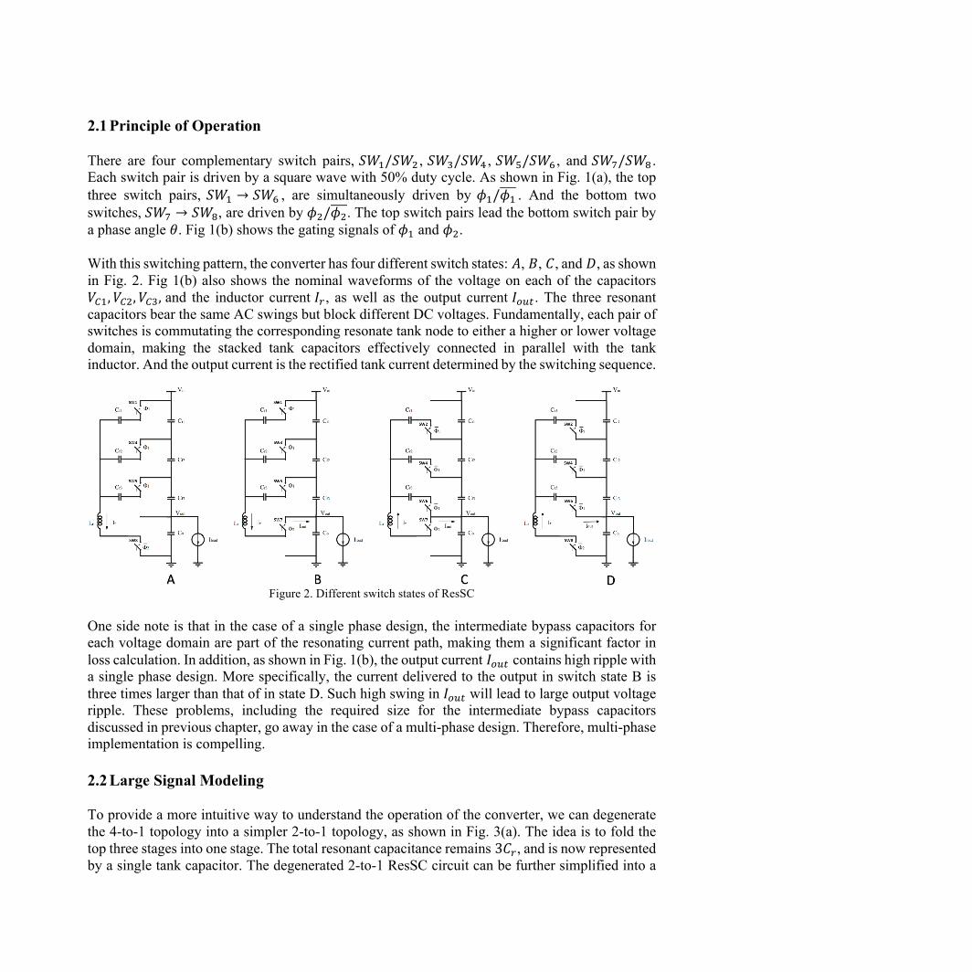
2.1 Principle of Operation There are four complementary switch pairs, 𝑆𝑊%/𝑆𝑊' , 𝑆𝑊(/𝑆𝑊6 , 𝑆𝑊7/𝑆𝑊8 , and 𝑆𝑊9/𝑆𝑊: . Each switch pair is driven by a square wave with 50% duty cycle. As shown in Fig. 1(a), the top three switch pairs, 𝑆𝑊% → 𝑆𝑊8 , are simultaneously driven by 𝜙%/𝜙% . And the bottom two switches, 𝑆𝑊9 → 𝑆𝑊:, are driven by 𝜙'/𝜙'. The top switch pairs lead the bottom switch pair by a phase angle 𝜃. Fig 1(b) shows the gating signals of 𝜙% and 𝜙'. With this switching pattern, the converter has four different switch states: 𝐴, 𝐵, 𝐶, and 𝐷, as shown in Fig. 2. Fig 1(b) also shows the nominal waveforms of the voltage on each of the capacitors 𝑉/%, 𝑉/', 𝑉/(, and the inductor current 𝐼- , as well as the output current 𝐼)*+ . The three resonant capacitors bear the same AC swings but block different DC voltages. Fundamentally, each pair of switches is commutating the corresponding resonate tank node to either a higher or lower voltage domain, making the stacked tank capacitors effectively connected in parallel with the tank inductor. And the output current is the rectified tank current determined by the switching sequence.
Figure 2. Different switch states of ResSC
One side note is that in the case of a single phase design, the intermediate bypass capacitors for each voltage domain are part of the resonating current path, making them a significant factor in loss calculation. In addition, as shown in Fig. 1(b), the output current 𝐼)*+ contains high ripple with a single phase design. More specifically, the current delivered to the output in switch state B is three times larger than that of in state D. Such high swing in 𝐼)*+ will lead to large output voltage ripple. These problems, including the required size for the intermediate bypass capacitors discussed in previous chapter, go away in the case of a multi-phase design. Therefore, multi-phase implementation is compelling. 2.2 Large Signal Modeling To provide a more intuitive way to understand the operation of the converter, we can degenerate the 4-to-1 topology into a simpler 2-to-1 topology, as shown in Fig. 3(a). The idea is to fold the top three stages into one stage. The total resonant capacitance remains 3𝐶-, and is now represented by a single tank capacitor. The degenerated 2-to-1 ResSC circuit can be further simplified into a

model as indicated in Fig. 3(b). Considering only the fundamental with a high Q tank, we can use the phasor diagram to represent the driving signals at node X and Y and all tank properties: 𝑉C, 𝑉E, 𝐼2 and 𝑉F. Fig. 3(c) shows the phasor diagram of the degenerated resonant tank. 𝑉C (the sending phasor) and 𝑉E (the receiving phasor) represent phasor voltages of two driving sources. 𝑉F represents the phasor of the net voltage applied voltage on the tank, which is the difference between 𝑉C and 𝑉E. 𝐼2 represents the phasor of inductor current, which is nominally perpendicular to the tank voltage 𝑉F for a high Q system. Phase angle 𝜃 is the phase difference between the two driving sources, which is set by the gating signal 𝜙% and 𝜙'. In order to make zero voltage switching (ZVS) for all switches to improve efficiency, the zero crossing of the resonant current should happen within switch states A or C [10]. In phasor domain, this means 𝐼2 should always be constrained within the phase angle 𝜃 . Therefore, based on trigonometry properties, the relation between phase angle 𝜃 and the optimal 4-to-1 output voltage range is given in Eq. 1. In the case of the proposed 4-to-1 prototype, the phase angle is chosen to be 45 degrees.
Figure 3. The degenerated 2-to-1 ResSC model (a), a simplified model of the 2-to-1 ResSC (b), and the phasor
representation under different operating condition (c) 𝑉"# cos 𝜃
3 + cos 𝜃 < 𝑉)*+ <𝑉"#
1 + 3cos 𝜃 (1)

The next step is to obtain an analytic expression for the steady state operation, which has already been derived in [10] and is shown in Eq. 2. The output current 𝐼)*+ is a function of the switching frequency 𝜔, phase angle 𝜃, 𝑉)and 𝑉"#. Given a preferred output voltage range for an application, the phase angle is set to achieve maximum efficiency. Since the input voltage is also pre-defined by application, the switching frequency remains to be the ideal control input for dynamic output regulation. 𝐼)*+ = −
2𝐶-𝜋'
𝜔𝑓%' 𝜔 + 𝑓'' 𝜔
[sin 𝜃 𝑉"#𝑓%'(𝜔) − (1 + cos 𝜃)(𝑉"# − 2𝑉)) 𝑓'(𝜔)] (2)
Where 𝑓% 𝜔 = 1 − YZ
Y[Z and 𝑓' 𝜔 = Y
Y[\ .
2.3 Small Signal Modeling Based on the small signal model derived in [10], the Bode plots of the transfer function for the proposed prototype are shown in Fig. 4. The blue line represents the transfer function from switching frequency to the phase of the resonant current, denoted by 𝐻Y→^. Similarly, the red line represents the transfer function from switching frequency to output voltage, denoted by 𝐻Y→_̀ .
Figure 4. Bode Plot of 𝐻Y→^(blue) and 𝐻Y→_̀ (red)
Looking at 𝐻Y→_̀ , there is a dominant pole introduced by the output capacitor at around 3 kHz, contributing a 90° phase lag and magnitude drop, followed by two complex conjugate poles, contributing another 180° phase lag and a large resonant peak in the magnitude response around

40 kHz. Looking at 𝐻Y→^, there is also a dominant pole caused by the output capacitor around the same frequency, making the initial roll off in magnitude and phase. However, for 𝐻Y→^ , the dominant pole is followed by two complex conjugate zeros, contributing not only an increase in the magnitude, but also a significant amount of phase lead. The control loop can take advantage of the phase lead generated by the zeros to increase the crossover frequency for better control dynamic. 2.4 Controller Design The proposed control designed then is as follows. In addition to the voltage loop, a phase minor loop is used to stabilize the system. More specifically, a proportional voltage loop is used to regulate the output voltage to a desired reference; a proportional phase loop is used to provide phase lead for stability. Fig. 5 shows the simulated 𝐻Y→_̀ Body plot before and after compensation with minor phase loop. As we can see, the dynamics from switching frequency to output voltage 𝐻Y→_̀ is stabilized with a phase margin of 36°. It also has a DC gain of 20.9 dB, which is independently adjustable by varying the proportionality in the voltage loop.
Figure 5. Bode Plot of 𝐻Y→_̀ before (blue) and after (red) minor phase loop compensation
3 Circuit Implementation
The design of the 4-to-1 ResSC converter prototype is divided into three parts. First is the power train design, which details how the switches and tank passives are sized and selected to achieve a desired function. Then a gate drive circuitry is proposed to actuate the power train, followed by a sensing network and a controller realization to close the loop. The general specifications for the prototype are shown in Table 1.

𝑉"# 24 V 𝑉)*+ 6 V 𝐼a)bc 2 A
𝐶- 100 nF 𝐿- 4.7 uH 𝑓-de 134 kHz
Table 1. 4-to-1 ResSC converter prototype general specifications
3.1 Power Train The loss of the system is mainly contributed by two parts. One is conduction loss and the other one is switching loss. Conduction loss is mainly caused by the series resistance of the switches and the tank passives. The current flow through these components will be intensive and thus care must be taken to minimize the effect. On the other hand, assuming ZVS, switching loss is mainly caused by the gate capacitance of the switches. Each time a switch alters its state, its gate capacitor needs to be charged or discharged accordingly. Thus, switching loss is closely associated with the switching frequency and the gate capacitance. The method to achieve a high efficiency is to balance the loss contribution from each part.
Figure 6. Output current waveform revisit (also shown in Fig. 1b)
In order to calculate the conduction loss, the root-mean-square of the tank current must be obtained first. And if we consider only the fundamental of the tank current in a high Q system, i.e. neglecting the harmonics introduced by phase shift in the control signal, the root-mean-square is just the magnitude divided by square root of two. Since we know the output current 𝐼)*+ is a partially rectified tank current as shown in Fig. 6, the average output current 𝐼)*+ can be obtained by averaging 𝐼)*+over a period. Note that the output current in switch state B is three times larger than that of in state D.
𝐼)*+ fg =1𝜋 𝐼h sin 𝜔𝑡 −
𝜃2 𝑑(𝜔𝑡)
k
^ (3)
𝐼)*+ /l =
1𝜋
13 𝐼h sin 𝜔𝑡 −
𝜃2 𝑑(𝜔𝑡)
k
^ (4)
Where 𝐼h is the the magnitude of the tank current. By solving Eq. 3 and 4, we have a unique relation between 𝐼)*+ and 𝐼h as shown in Eq. 5. And since 𝐼)*+ must be the load current for the converter, which has a rated value of 2A in this prototype, the magnitude and thus the root-mean-square of the tank current can be obtained as shown in Eq. 6.

𝐼)*+ =𝐼)*+ fg + 𝐼)*+ /l
2 =2𝐼h𝜋 cos 𝜃2 (1 +
13)
2 =43𝜋 cos
𝜃2 ∙ 𝐼h (5)
𝐼-ne =
𝐼h2=
3𝜋
4 2 cos 𝜃2∙ 𝐼)*+ (6)
The conduction loss of a 4-to-1 topology is calculated as shown in Eq. 7. Note that the current flowing through the top three switch pairs is one third of 𝐼-ne as discussed previously. The current flowing through the bottom switch pair, on the other hand, will be the full 𝐼-ne.
𝑃p)#c = 3 ⋅ 𝑅stuv`w𝐼-ne3
'
+ 𝑅stux`v𝐼-ne' (7)
The switching loss of a 4-to-1 topology is calculated according to Eq. 8. All of the eight switches will have nominally the same switching loss. The 𝐶y term represents the gate capacitance for each switch and 𝑉y is the voltage swing on the gate of each switch. The drain capacitance is ignored because of ZVS. Note that even though each switch is operating in its own respective voltage domain, the gate voltage swing is constant for all switches as guaranteed by the gate drive circuitry. The overall efficiency then is obtained with Eq. 9. 𝑃ez = 8 ⋅ 𝑓ez𝐶y𝑉y' (8)
𝜂 =
𝑉)*+ ⋅ 𝐼)*+𝑃a)ee,+)+ + 𝑉)*+ ⋅ 𝐼)*+
=1
1 + 𝑃ez + 𝑃p)#c𝑉)*+ ⋅ 𝐼)*+
(9)
3.2 Gate Drive One of the problem that a gate drive circuitry must solve is gating high-side switches. In the case of MOSFET implementation, a high-side switch is a MOSFET whose source is floating. Obviously, in order to operate the device in the saturation region, the gate voltage must be at least a 𝑉+} higher (oftentimes much higher when the device is considered as a switch) than the source voltage. A similar consideration applies for turning off the device. But when the source is floating, the gate voltage also needs to be floating accordingly to have predictable behaviors for the device. Therefore, the gate drive circuity must dynamically change the gate voltage with respect to the source voltage so that the device can remain on or off. To make life easier, our gate drive circuitry design takes advantage of the fact that there are four relatively stable voltage domains in the power train topology. By using a PMOS and a NMOS for each switch pair, where the NMOS will have its source connected to the lower voltage domain and that of the PMOS to the higher voltage domain, the gate drive circuitry only needs to pass the gating signals to the corresponding voltage domain to deterministically turn on or off the switches. The proposed design schematic is shown in Fig. 7. A flying capacitor 𝐶~a� is connected to the gate

of each high-side switch and it is initially charged up from GND to the corresponding voltage domain. The diode and 𝑅�"y are the DC charging path for 𝐶~a� , which acts as a DC blocking capacitor at high frequency. 𝑅cbn� is to damp any oscillation caused by the gate drive loop inductance.
Figure 7. The implementation of gate drive for the power train
3.3 Controller The schematic of the proposed controller is shown in Fig. 8(a). As discussed in the previous chapter, the controller consists of two loops: a voltage loop and a current phase loop. The voltage loop takes the output voltage 𝑉)*+, divides it by an adjustable factor, subtracts it from the reference, and amplifies the error. The gain of the voltage loop should be maximized for small DC error at the output. This is one of the classic textbook feedback schemes with a proportional gain and is not hard implement at all. The real challenge, however, lies in the current phase loop.

In order to obtain the phase of the tank current, one must extract the resonant current first. The resonant current 𝐼- is sensed by using a transformer formed with the resonant inductor as the primary side, and a secondary sense winding that accesses the pure inductive voltage component. Since we know c�0
c+= ��
2, a passive integrator following the sensing transformer is used to integrate
the voltage. It then generates the replica of the resonant current with a scaling factor of ���Z⋅ 20u��v/��v
, where 𝑅"#+ and 𝐶"#+ are the integrator’s passives.
Figure 8. The implementation of the control circuit (a) and the representative waveforms of phase error detector (b) The phase error is then extracted by using a passive mixer, which compares the replicated current 𝑉h with a clock reference 𝜙(. The relative phase shift of the reference clock 𝜙( with respect to the gating of the power train 𝜙% and 𝜙' is shown in Fig. 8(b). In this way, the phase error can be approximated as the DC average of the mixer output 𝑉�} , which is then amplified by the succeeding op-amp. The gain of the minor phase loop is selected so that the closed-loop system is stable and well compensated. In the last part of the control loop, the amplified phase error is combined with the amplified voltage error and is fed into the VCO, which generates the system clock frequency according to the input error signal level. A FPGA is then used to generate all the necessary gate signals from the VCO output for all the switches within the power train as well as the reference clock needed in phase loop.
4 Experimental Results
A prototype of 4-to-1 resonant switch capacitor converter is built with a nominal 6W output power. The project specification is shown in Table. 2 and the selection of the components is shown in Table. 3. The switching frequency has chosen to be around 170 kHz and it yields an acceptable

switching loss. Low parasitic resistance switches are chosen to minimize conduction loss. The efficiency target is around 90%.
Table 2. Project Specification
Table 3. The Selection of Components
Fig. 9(A) and Fig. 9(B) reflect how the switching frequency can effectively modulate the output voltage given a certain load condition, and regulate the output current under different voltages respectively. Fig. 9(C) shows the efficiency vs. the output voltage with the nominal load condition and Fig. 9(D) shows the efficiency vs. the output current with the nominal output voltage condition. We can see that for an output range of 4V to 8V, the converter can comfortably maintain efficiency above 85% with a peak efficiency of 93% at the nominal 6V output. And for an output of 300mA to 1.8A, the converter can also sustain high efficiency.
Figure 9. Switching frequency vs output voltage with 1A load (A), switching frequency vs load current with 6V output (B), Efficiency vs the output voltage with 1A load (C), and efficiency vs load current with 6V output (D).

Fig. 10 shows the experimental waveform of 𝜙% and 𝜙' , which are the gating signals at the switching nodes of the top three switch pairs and the bottom switch pair respectively. The inductor current 𝐼- waveform is also shown on the same plot. We can see the zero crossing of the current is aligned within the interval set by the top and the bottom switching actions (i.e. switch states A or C) as shown in Fig. 1(b). This verifies that the control signal is making ZVS for all switches.
Figure 10. The steady state waveforms of the switching node voltage of the bottom section (yellow), the third
section (pink) and the sensing voltage of the resonate current (green)
The effectiveness of the controller is demonstrated in Fig. 11, which shows the transient performance of the output with a load step. This is a 1A load step, up and down. The DC voltage offset presented at the output is around 300mV, while the transient time is about 20us. The amplified voltage error as well as the amplified current phase error are shown on the same plot.
Figure 11. The transient waveforms of the output voltage (blue), phase error signal (yellow), voltage error (green)
under the load steps (triggered by the pink signal) of 0.5A to 1.5A and 1.5A to 0.5A

A more insightful method to evaluate the effectiveness of the control is by plotting out the state contour for the converter as described in [11]. A state contour plots on a plane that has the instantaneous resonating current as the vertical axis and the instantaneous resonating voltage as the horizontal axis. As shown in Fig. 12, a step up load transient state contour is represented by the blue line. The two red circles show the two theoretical steady states at light and full load respectively from simulation. Initially, the state contour spins around the inner red circle clockwise as the load is light. Once the step trigger kicks in, the state contour start spinning outward. It eventually settles down at the outer red circle as its new steady state. The number of circles it takes to transit from the inner to the outer circle is directly related to the transient performance.
Figure 12. Experimental state contour during transient (blue) and theoretical state contour at different steady states
(red)
5 Conclusion
Fully integrated dc-dc conversion is the future for power management in portable devices. Switched-capacitor topology utilizes capacitor that has superior energy density compared to that of inductor. As shown in Table. 4, the energy densities of some representative surface mount capacitors are significantly grater than those of inductors [1]. Such properties of capacitors are the cornerstone for eliminating the large area that was traditionally occupied by the bulky inductors in the buck converter.

Table 4. Dimensions and volumetric energy densities of some representative surface mount capacitors and inductors [1]
The switched-capacitor (SC) based power converter, however, has its own drawback. Its limited output range and its intrinsic charge-sharing loss has prevented it from being widely adopted. Fig. 13 shows the efficiency of SC converters with 2:1, 3:1, and 3:2 conversion ratios [12]. The efficiency drops dramatically when the output voltages deviate from the nominal values, which limits the output range of the converters. The fundamental cause of the problem is the intrinsic charge-sharing loss of capacitors.
Figure 13. The efficiency plot of nominal 2:1, 3:1, and 3:2 SC converters with a 2V input [12]
In this work, a stackable resonant switched-capacitor (ResSC) topology is introduced as a viable approach to further refine SC methodology for a wide range of applications. More specifically, by introducing a small inductor in series with the flying capacitors, the charge-sharing loss is eliminated and thus, the converter can support a much wider output range while maintaining high efficiency as shown in Fig. 9(c). With a stackable architecture, the conversion ratios can be optimized to further improve efficiency. Therefore, the ResSC not only has the same promise for compact, fully integrated dc-dc converters as does the SC methodology, but also allows nominal lossless power management to support wider application.

References [1] S. Sanders, E. Alon, H.-P. Le, M. Seeman, M. John, and V. Ng, “The road to fully integrated dc-dc conversion
via the switched-capacitor approach,” Power Electronics, IEEE Transactions on, vol. 28, pp. 4146–4155, Sept 2013.
[2] H.-P. Le, S. Sanders, and E. Alon, “Design techniques for fully integrated switched-capacitor dc-dc converters,” Solid-State Circuits, IEEE Journal of, vol. 46, pp. 2120–2131, Sept 2011.
[3] M. Seeman and S. Sanders, “Analysis and optimization of switched-capacitor dc-dc converters,” Power Electronics, IEEE Transactions on, vol. 23, pp. 841–851, March 2008.
[4] K. Kesarwani, R. Sangwan, and J. Stauth, “Resonant switched-capacitor converters for chip-scale power delivery: Modeling and design,” in Control and Modeling for Power Electronics (COMPEL), 2013 IEEE 14th Workshop on, pp. 1–7, June 2013.
[5] Y. Lei and R. Pilawa-Podgurski, “A general method for analyzing resonant and soft-charging operation of switched-capacitor converters,” Power Electronics, IEEE Transactions on, vol. 30, pp. 5650–5664, Oct 2015.
[6] K. Sano and H. Fujita, “Performance of a high-efficiency switched-capacitor-based resonant converter with phase-shift control,” Power Electronics, IEEE Transactions on, vol. 26, pp. 344–354, Feb 2011.
[7] Y. Lei, R. May, and R. Pilawa-Podgurski, “Split-phase control: Achieving complete soft-charging operation of a dickson switched- capacitor converter,” Power Electronics, IEEE Transactions on, vol. PP, no. 99, pp. 1–1, 2015.
[8] K. Kesarwani, R. Sangwan, and J. Stauth, “Resonant switched-capacitor converters for chip-scale power delivery: Design amp; implementation,” Power Electronics, IEEE Transactions on, vol. PP, no. 99, pp. 1–1, 2014.
[9] A. Cervera, M. Evzelman, M. Peretz, and S. Ben-Yaakov, “A high-efficiency resonant switched capacitor converter with continuous conversion ratio,” Power Electronics, IEEE Transactions on, vol. 30, pp. 1373–1382, March 2015.
[10] Y. Li, M. John, J. Poon, J. Chen, and S. Sanders, “Lossless voltage regulation and control of the resonant switched-capacitor dc-dc converter,” in Control and Modeling for Power Electronics (COMPEL), 2015 IEEE 16th Workshop on, pp. 1–7, July 2015.
[11] W. Feng, F. C. Lee, and P. Mattavelli, “A hybrid strategy with simplified optimal trajectory control for LLC resonant converters,” in Proc. IEEE Appl. Power Electron. Conf., Feb. 2012, pp. 1096–1103.
[12] H.-P. Le, S. R. Sanders, and E. Alon, “Design techniques for fully integrated switched-capacitor DC-DC converters,” IEEE J. Solid-State Circuits, vol. 46, no. 9, pp. 2120–2131, Sep. 2011.