Embed Size (px)
Citation preview
12/8/11
1
George Mason University
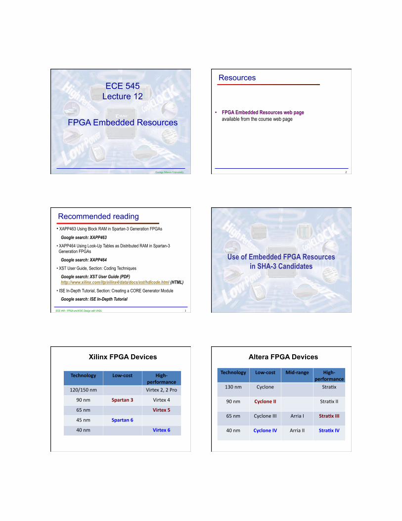
ECE 545 Lecture 12
FPGA Embedded Resources
2
Resources
• FPGA Embedded Resources web page available from the course web page
3 ECE 448 – FPGA and ASIC Design with VHDL
Recommended reading • XAPP463 Using Block RAM in Spartan-3 Generation FPGAs
Google search: XAPP463
• XAPP464 Using Look-Up Tables as Distributed RAM in Spartan-3 Generation FPGAs
Google search: XAPP464
• XST User Guide, Section: Coding Techniques
Google search: XST User Guide (PDF) http://www.xilinx.com/itp/xilinx4/data/docs/xst/hdlcode.html (HTML)
• ISE In-Depth Tutorial, Section: Creating a CORE Generator Module
Google search: ISE In-Depth Tutorial
ECE 448 – FPGA and ASIC Design with VHDL
Use of Embedded FPGA Resources in SHA-3 Candidates
Technology Low-‐cost High-‐performance
120/150 nm Virtex 2, 2 Pro
90 nm Spartan 3 Virtex 4
65 nm Virtex 5
45 nm Spartan 6
40 nm Virtex 6
Xilinx FPGA Devices Altera FPGA Devices
Technology Low-‐cost Mid-‐range High-‐performance
130 nm Cyclone StraKx
90 nm Cyclone II StraKx II
65 nm Cyclone III Arria I StraAx III
40 nm Cyclone IV Arria II StraAx IV
12/8/11
2
ECE 448 – FPGA and ASIC Design with VHDL
FPGA Embedded Resources
ECE 448 – FPGA and ASIC Design with VHDL
Embedded Multipliers
10 ECE 448 – FPGA and ASIC Design with VHDL
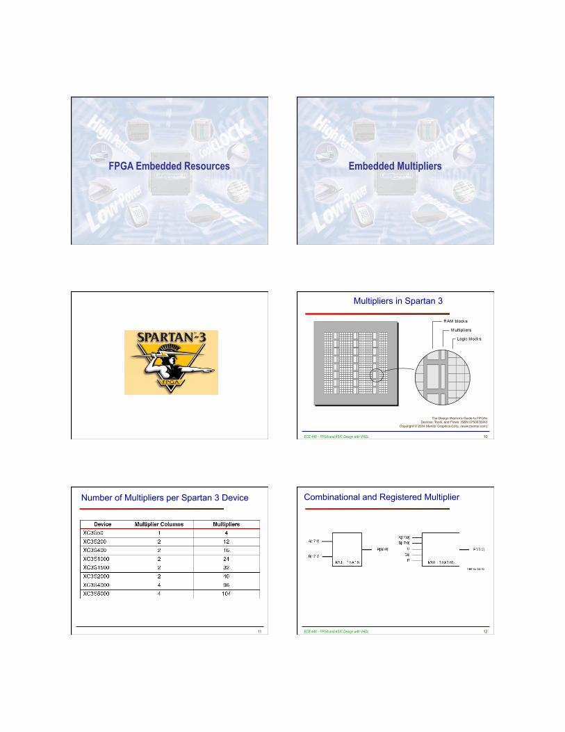
Multipliers in Spartan 3
The Design Warrior’s Guide to FPGAs Devices, Tools, and Flows. ISBN 0750676043
Copyright © 2004 Mentor Graphics Corp. (www.mentor.com)
11
Number of Multipliers per Spartan 3 Device
12
Combinational and Registered Multiplier
ECE 448 – FPGA and ASIC Design with VHDL
12/8/11
3
13 ECE 448 – FPGA and ASIC Design with VHDL
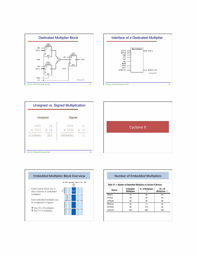
Dedicated Multiplier Block
14 ECE 448 – FPGA and ASIC Design with VHDL
Interface of a Dedicated Multiplier
15 ECE 448 – FPGA and ASIC Design with VHDL
Unsigned vs. Signed Multiplication
1111
1111 x
11100001
15
15 x
225
1111
1111 x
00000001
-1
-1 x
1
Unsigned Signed
Cyclone II
Embedded MulKplier Block Overview
Each Cyclone II has one to three columns of embedded multipliers.
Each embedded multiplier can be configured to support
One 18 x 18 multiplier Two 9 x 9 multipliers
Number of Embedded MulKpliers
12/8/11
4
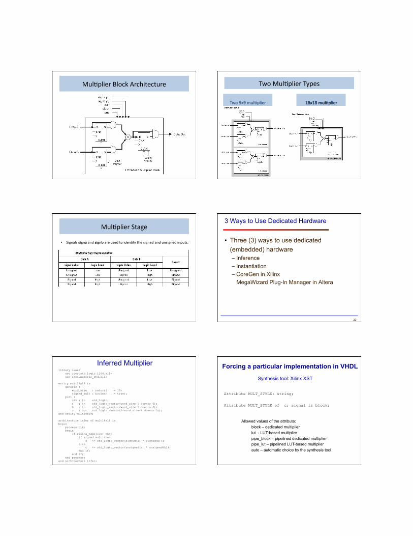
MulKplier Block Architecture Two MulKplier Types
MulKplier Stage
• Signals signa and signb are used to idenKfy the signed and unsigned inputs.
22
3 Ways to Use Dedicated Hardware
• Three (3) ways to use dedicated (embedded) hardware
– Inference – Instantiation – CoreGen in Xilinx MegaWizard Plug-In Manager in Altera
library ieee; use ieee.std_logic_1164.all; use ieee.numeric_std.all;
entity mult18x18 is generic ( word_size : natural := 18; signed_mult : boolean := true); port ( clk : in std_logic; a : in std_logic_vector(word_size-1 downto 0); b : in std_logic_vector(word_size-1 downto 0); c : out std_logic_vector(2*word_size-1 downto 0)); end entity mult18x18;
architecture infer of mult18x18 is begin process(clk) begin if rising_edge(clk) then if signed_mult then c <= std_logic_vector(signed(a) * signed(b)); else c <= std_logic_vector(unsigned(a) * unsigned(b)); end if; end if; end process; end architecture infer;
Inferred Multiplier Forcing a particular implementation in VHDL
Synthesis tool: Xilinx XST
Attribute MULT_STYLE: string;
Attribute MULT_STYLE of c: signal is block;
Allowed values of the attribute: block – dedicated multiplier lut - LUT-based multiplier pipe_block – pipelined dedicated multiplier pipe_lut – pipelined LUT-based multiplier auto – automatic choice by the synthesis tool
12/8/11
5
Instantiation for Spartan 3 FPGAs CORE Generator
ECE 448 – FPGA and ASIC Design with VHDL
DSP Units
28
Xilinx XtremeDSP
• Starting with Virtex 4 family, Xilinx introduced DSP48 block for high-speed DSP on FPGAs
• Essentially a multiply-accumulate core with many other features
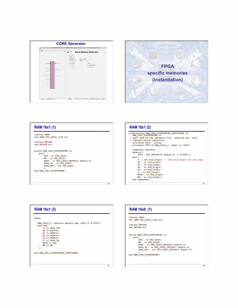
• Now also in Spartan-3A, Spartan 6, Virtex 5, and Virtex 6
29
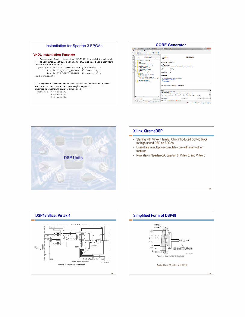
DSP48 Slice: Virtex 4
30
Simplified Form of DSP48
Adder Out = (Z ± (X + Y + CIN))
12/8/11
6
31
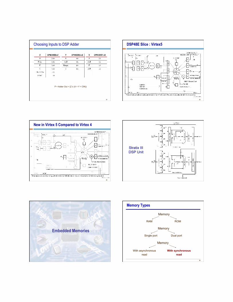
Choosing Inputs to DSP Adder
P = Adder Out = (Z ± (X + Y + CIN))
32
DSP48E Slice : Virtex5
33
New in Virtex 5 Compared to Virtex 4
Stratix III DSP Unit
ECE 448 – FPGA and ASIC Design with VHDL
Embedded Memories
36
Memory Types
Memory
RAM ROM
Single port Dual port
With asynchronous read
With synchronous read
Memory
Memory
12/8/11
7
37
Memory Types in Xilinx
Memory
Distributed (MLUT-based)
Block RAM-based (BRAM-based)
Inferred Instantiated
Memory
Manually Using Core Generator
38
Memory Types in Altera
Memory
Distributed (ALUT-based,
Stratix III onwards)
Memory block-based
Inferred Instantiated
Memory
Manually Using MegaWizard Plug-In Manager
Small size (512)
Large size (144K, 512K)
Medium size (4K, 9K, 20K)
39
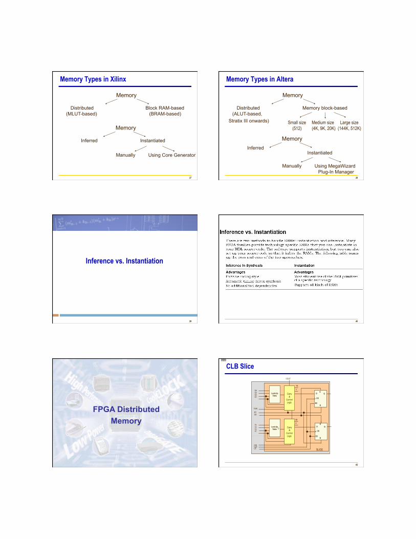
Inference vs. Instantiation
40
41
FPGA Distributed Memory
42
COUT
D Q
CK
S
R EC
D Q
CK
R EC
O
G4 G3 G2 G1
Look-Up Table Carry
& Control Logic
O
YB
Y
F4 F3 F2 F1
XB X
Look-Up Table
F5IN
BY SR
S
Carry &
Control Logic
CIN CLK CE SLICE
CLB Slice
12/8/11
8
43
The Design Warrior’s Guide to FPGAs Devices, Tools, and Flows. ISBN 0750676043
Copyright © 2004 Mentor Graphics Corp. (www.mentor.com)
Xilinx Multipurpose LUT
44
RAM16X1S
O
DWE
WCLK A0 A1 A2 A3
RAM32X1S
O
DWE WCLK A0 A1 A2 A3 A4
RAM16X2S
O1
D0
WE WCLK A0 A1 A2 A3
D1
O0
=
= LUT
LUT or
LUT
RAM16X1D
SPO
DWE
WCLK A0 A1 A2 A3 DPRA0 DPO DPRA1 DPRA2 DPRA3
or
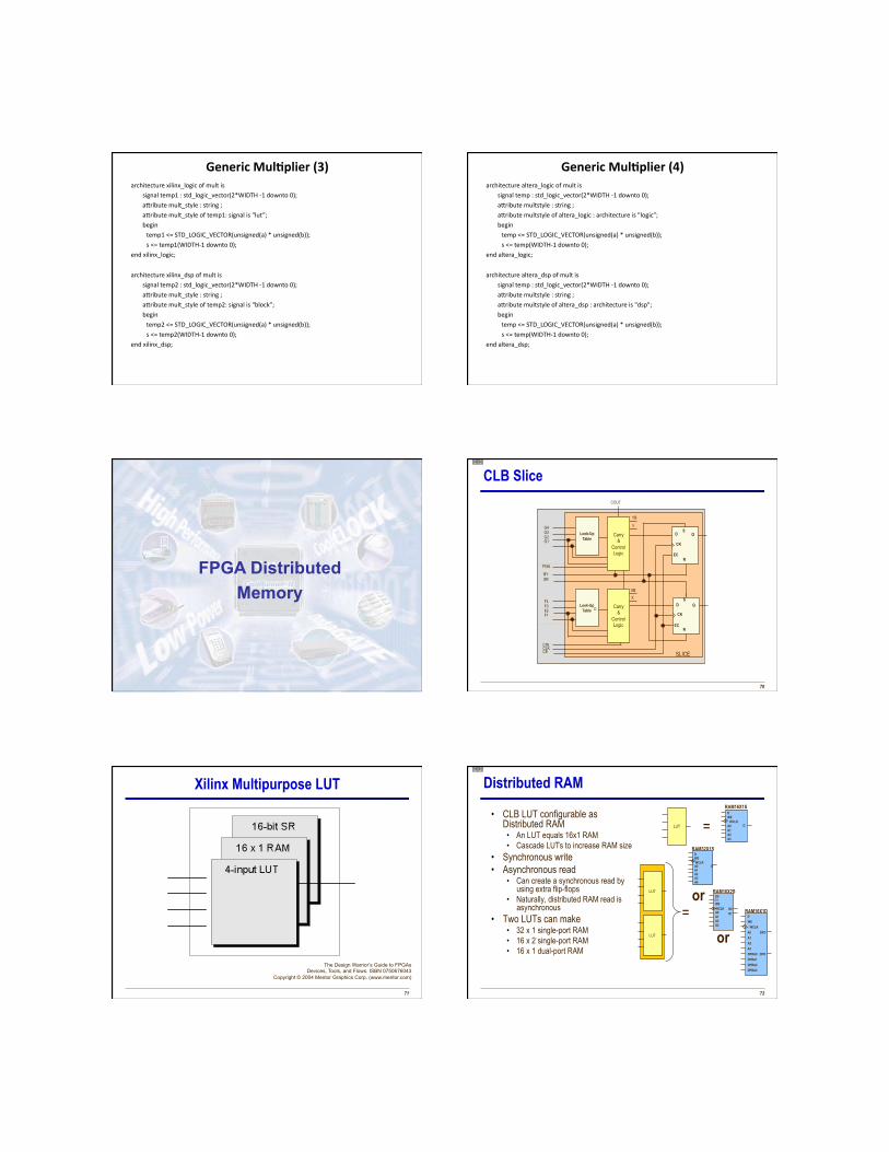
Distributed RAM
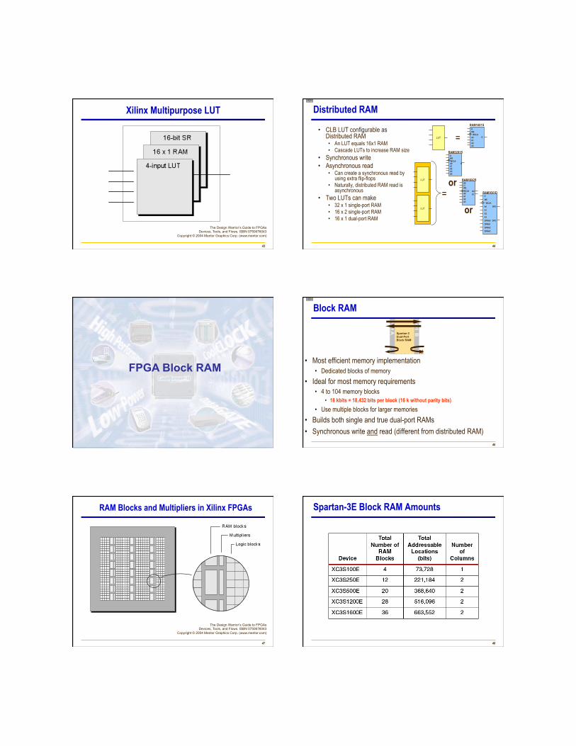
• CLB LUT configurable as Distributed RAM • An LUT equals 16x1 RAM • Cascade LUTs to increase RAM size
• Synchronous write • Asynchronous read
• Can create a synchronous read by using extra flip-flops
• Naturally, distributed RAM read is asynchronous
• Two LUTs can make • 32 x 1 single-port RAM • 16 x 2 single-port RAM • 16 x 1 dual-port RAM
45
FPGA Block RAM
46
Block RAM
Spartan-3 Dual-Port Block RAM
Port A
Port B
Block RAM
• Most efficient memory implementation • Dedicated blocks of memory
• Ideal for most memory requirements • 4 to 104 memory blocks
• 18 kbits = 18,432 bits per block (16 k without parity bits) • Use multiple blocks for larger memories
• Builds both single and true dual-port RAMs • Synchronous write and read (different from distributed RAM)
47
RAM Blocks and Multipliers in Xilinx FPGAs
The Design Warrior’s Guide to FPGAs Devices, Tools, and Flows. ISBN 0750676043
Copyright © 2004 Mentor Graphics Corp. (www.mentor.com)
48
Spartan-3E Block RAM Amounts
12/8/11
9
49
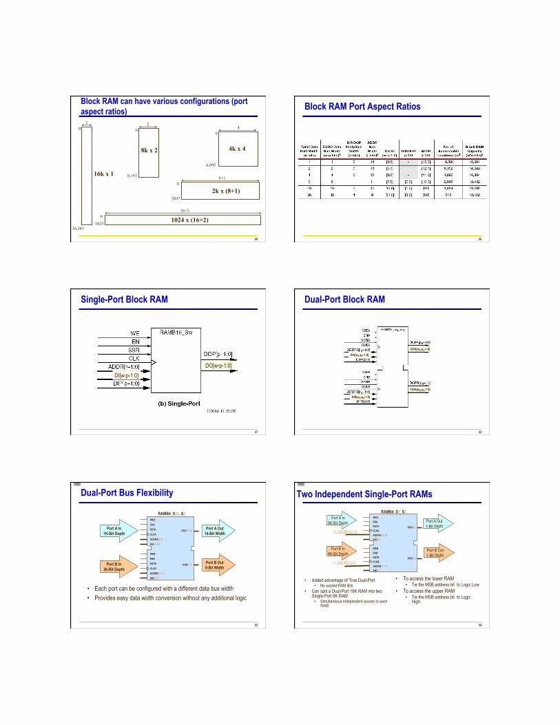
Block RAM can have various configurations (port aspect ratios)
0
16,383
1
4,095
4 0
8,191
2 0
2047
8+1 0
1023
16+2 0
16k x 1
8k x 2 4k x 4
2k x (8+1)
1024 x (16+2)
50
Block RAM Port Aspect Ratios
51
Single-Port Block RAM
DI[w-p-1:0] DO[w-p-1:0]
52
Dual-Port Block RAM
DIA[wA-pA-1:0]
DOA[wA-pA-1:0]
DOA[wB-pB-1:0]
DIB[wB-pB-1:0]
53
RAMB4_S18_S9
Port A Out 18-Bit Width
Port B In 2k-Bit Depth
Port A In 1K-Bit Depth
Port B Out 9-Bit Width
DOA[17:0]
DOB[8:0]
WEA
ENA
RSTA
ADDRA[9:0]
CLKA
DIA[17:0]
WEB
ENB
RSTB
ADDRB[10:0]
CLKB
DIB[8:0]
Dual-Port Bus Flexibility
• Each port can be configured with a different data bus width • Provides easy data width conversion without any additional logic
54
0, ADDR[12:0]
1, ADDR[12:0]
RAMB4_S1_S1
Port B Out 1-Bit Width
DOA[0]
DOB[0]
WEA ENA RSTA
ADDRA[12:0] CLKA
DIA[0]
WEB ENB RSTB
ADDRB[12:0] CLKB
DIB[0]
Port B In 8K-Bit Depth
Port A Out 1-Bit Width
Port A In 8K-Bit Depth
Two Independent Single-Port RAMs
• To access the lower RAM • Tie the MSB address bit to Logic Low
• To access the upper RAM • Tie the MSB address bit to Logic
High
• Added advantage of True Dual-Port • No wasted RAM Bits
• Can split a Dual-Port 16K RAM into two Single-Port 8K RAM
• Simultaneous independent access to each RAM
12/8/11
10
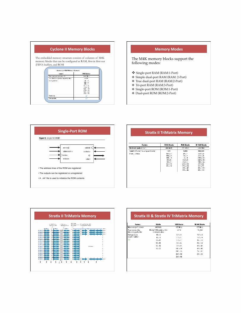
The embedded memory structure consists of columns of M4K memory blocks that can be configured as RAM, first-in first-out (FIFO) buffers, and ROM
Cyclone II Memory Blocks
The M4K memory blocks support the following modes:!
Single-port RAM (RAM:1-Port)! Simple dual-port RAM (RAM: 2-Port)! True dual-port RAM (RAM:2-Port)! Tri-port RAM (RAM:3-Port)! Single-port ROM (ROM:1-Port)! Dual-port ROM (ROM:2-Port)!
Memory Modes
Single-‐Port ROM
• The address lines of the ROM are registered
• The outputs can be registered or unregistered
• A .mif file is used to initialize the ROM contents
StraAx II TriMatrix Memory
StraAx II TriMatrix Memory StraAx III & StraAx IV TriMatrix Memory
12/8/11
11
StraAx II & III ShiI-‐Register Memory ConfiguraAon
ECE 448 – FPGA and ASIC Design with VHDL
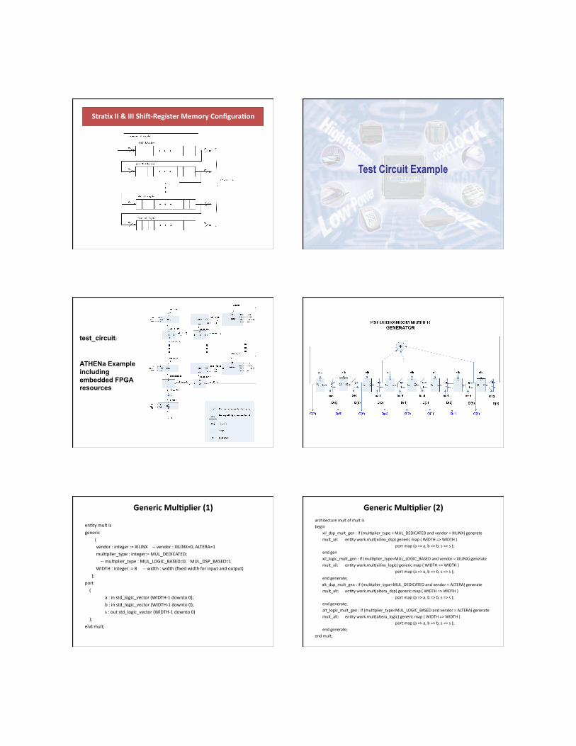
Test Circuit Example
ATHENa Example including embedded FPGA resources
test_circuit:
Generic MulAplier (1)
enKty mult is
generic
( vendor : integer := XILINX -‐-‐ vendor : XILINX=0, ALTERA=1
mulKplier_type : integer:= MUL_DEDICATED;
-‐-‐ mulKplier_type : MUL_LOGIC_BASED=0, MUL_DSP_BASED=1
WIDTH : integer := 8 -‐-‐ width : width (fixed width for input and output)
);
port
(
a : in std_logic_vector (WIDTH-‐1 downto 0);
b : in std_logic_vector (WIDTH-‐1 downto 0);
s : out std_logic_vector (WIDTH-‐1 downto 0)
);
end mult;
Generic MulAplier (2) architecture mult of mult is begin
xil_dsp_mult_gen : if (mulKplier_type = MUL_DEDICATED and vendor = XILINX) generate
mult_xil: enKty work.mult(xilinx_dsp) generic map ( WIDTH => WIDTH )
port map (a => a, b => b, s => s );
end gen
xil_logic_mult_gen : if (mulKplier_type=MUL_LOGIC_BASED and vendor = XILINX) generate
mult_xil: enKty work.mult(xilinx_logic) generic map ( WIDTH => WIDTH )
port map (a => a, b => b, s => s );
end generate;
alt_dsp_mult_gen : if (mulKplier_type=MUL_DEDICATED and vendor = ALTERA) generate
mult_alt: enKty work.mult(altera_dsp) generic map ( WIDTH => WIDTH )
port map (a => a, b => b, s => s );
end generate;
alt_logic_mult_gen : if (mulKplier_type=MUL_LOGIC_BASED and vendor = ALTERA) generate
mult_alt: enKty work.mult(altera_logic) generic map ( WIDTH => WIDTH )
port map (a => a, b => b, s => s );
end generate;
end mult;
12/8/11
12
Generic MulAplier (3) architecture xilinx_logic of mult is
signal temp1 : std_logic_vector(2*WIDTH -‐1 downto 0);
afribute mult_style : string ;
afribute mult_style of temp1: signal is "lut”;
begin
temp1 <= STD_LOGIC_VECTOR(unsigned(a) * unsigned(b));
s <= temp1(WIDTH-‐1 downto 0);
end xilinx_logic;
architecture xilinx_dsp of mult is
signal temp2 : std_logic_vector(2*WIDTH -‐1 downto 0);
afribute mult_style : string ;
afribute mult_style of temp2: signal is "block”;
begin
temp2 <= STD_LOGIC_VECTOR(unsigned(a) * unsigned(b));
s <= temp2(WIDTH-‐1 downto 0);
end xilinx_dsp;
Generic MulAplier (4) architecture altera_logic of mult is
signal temp : std_logic_vector(2*WIDTH -‐1 downto 0);
afribute multstyle : string ;
afribute multstyle of altera_logic : architecture is "logic”;
begin
temp <= STD_LOGIC_VECTOR(unsigned(a) * unsigned(b));
s <= temp(WIDTH-‐1 downto 0);
end altera_logic;
architecture altera_dsp of mult is
signal temp : std_logic_vector(2*WIDTH -‐1 downto 0);
afribute multstyle : string ;
afribute multstyle of altera_dsp : architecture is "dsp";
begin
temp <= STD_LOGIC_VECTOR(unsigned(a) * unsigned(b));
s <= temp(WIDTH-‐1 downto 0);
end altera_dsp;
69
FPGA Distributed Memory
70
COUT
D Q
CK
S
R EC
D Q
CK
R EC
O
G4 G3 G2 G1
Look-Up Table Carry
& Control Logic
O
YB
Y
F4 F3 F2 F1
XB X
Look-Up Table
F5IN
BY SR
S
Carry &
Control Logic
CIN CLK CE SLICE
CLB Slice
71
The Design Warrior’s Guide to FPGAs Devices, Tools, and Flows. ISBN 0750676043
Copyright © 2004 Mentor Graphics Corp. (www.mentor.com)
Xilinx Multipurpose LUT
72
RAM16X1S
O
DWE
WCLK A0 A1 A2 A3
RAM32X1S
O
DWE WCLK A0 A1 A2 A3 A4
RAM16X2S
O1
D0
WE WCLK A0 A1 A2 A3
D1
O0
=
= LUT
LUT or
LUT
RAM16X1D
SPO
DWE
WCLK A0 A1 A2 A3 DPRA0 DPO DPRA1 DPRA2 DPRA3
or
Distributed RAM
• CLB LUT configurable as Distributed RAM • An LUT equals 16x1 RAM • Cascade LUTs to increase RAM size
• Synchronous write • Asynchronous read
• Can create a synchronous read by using extra flip-flops
• Naturally, distributed RAM read is asynchronous
• Two LUTs can make • 32 x 1 single-port RAM • 16 x 2 single-port RAM • 16 x 1 dual-port RAM
12/8/11
13
73
Inference vs.
Instantiation
74
75
Generic Inferred
RAM
76
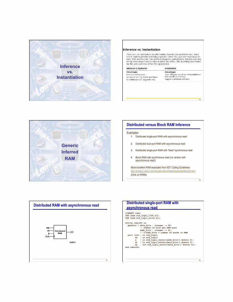
Distributed versus Block RAM Inference
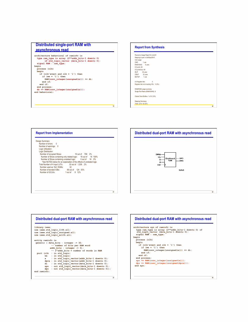
Examples: 1. Distributed single-port RAM with asynchronous read
2. Distributed dual-port RAM with asynchronous read
3. Distributed single-port RAM with "false" synchronous read
4. Block RAM with synchronous read (no version with asynchronous read!)
More excellent RAM examples from XST Coding Guidelines: http://toolbox.xilinx.com/docsan/xilinx4/data/docs/xst/hdlcode.html (Click on RAMs)
77
Distributed RAM with asynchronous read
78
Distributed single-port RAM with asynchronous read
LIBRARY ieee; USE ieee.std_logic_1164.all; USE ieee.std_logic_arith.all;
entity raminfr is generic ( data_bits : integer := 32; -- number of bits per RAM word addr_bits : integer := 3); -- 2^addr_bits = number of words in RAM port (clk : in std_logic; we : in std_logic; a : in std_logic_vector(addr_bits-1 downto 0); di : in std_logic_vector(data_bits-1 downto 0); do : out std_logic_vector(data_bits-1 downto 0)); end raminfr;
12/8/11
14
79
Distributed single-port RAM with asynchronous read
architecture behavioral of raminfr is type ram_type is array (2**addr_bits-1 downto 0) of std_logic_vector (data_bits-1 downto 0); signal RAM : ram_type; begin process (clk) begin if (clk'event and clk = '1') then if (we = '1') then RAM(conv_integer(unsigned(a))) <= di; end if; end if; end process; do <= RAM(conv_integer(unsigned(a))); end behavioral;
80
Report from Synthesis
Resource Usage Report for raminfr Mapping to part: xc3s50pq208-5 Cell usage: GND 1 use RAM16X4S 8 uses I/O ports: 69 I/O primitives: 68 IBUF 36 uses OBUF 32 uses BUFGP 1 use
I/O Register bits: 0 Register bits not including I/Os: 0 (0%)
RAM/ROM usage summary Single Port Rams (RAM16X4S): 8
Global Clock Buffers: 1 of 8 (12%)
Mapping Summary: Total LUTs: 32 (2%)
81
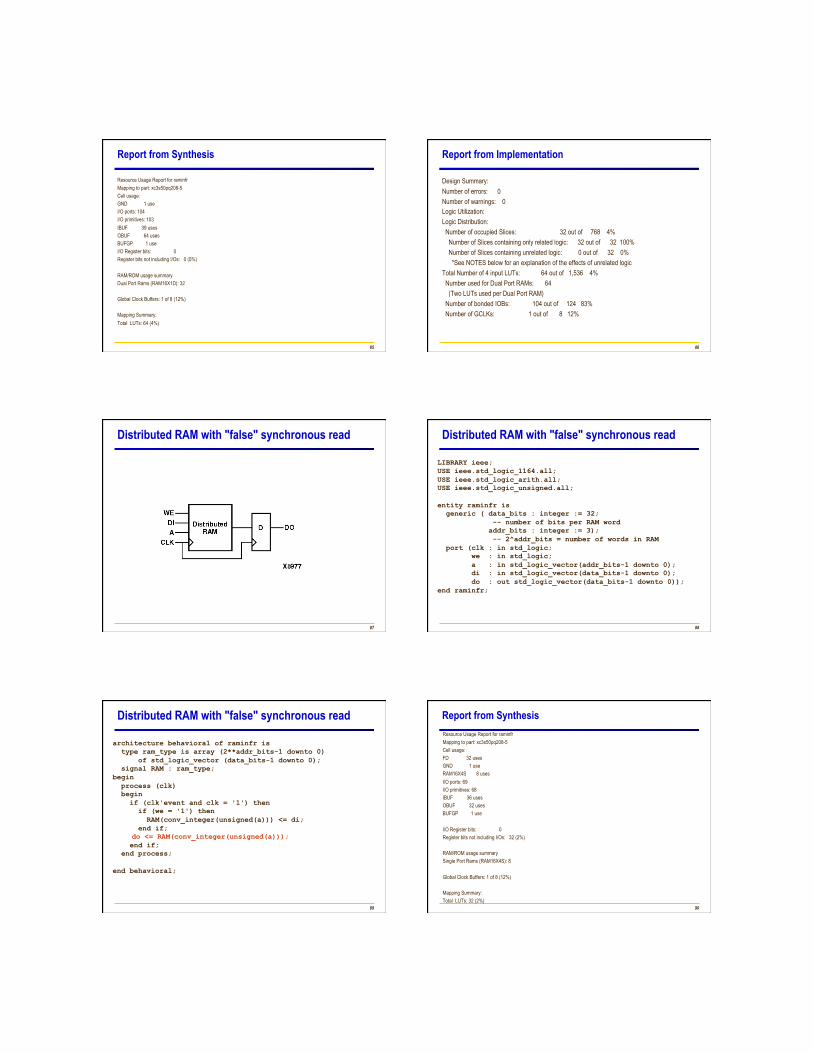
Report from Implementation
Design Summary: Number of errors: 0 Number of warnings: 0 Logic Utilization: Logic Distribution: Number of occupied Slices: 16 out of 768 2% Number of Slices containing only related logic: 16 out of 16 100% Number of Slices containing unrelated logic: 0 out of 16 0% *See NOTES below for an explanation of the effects of unrelated logic Total Number of 4 input LUTs: 32 out of 1,536 2% Number used as 16x1 RAMs: 32 Number of bonded IOBs: 69 out of 124 55% Number of GCLKs: 1 out of 8 12%
82
Distributed dual-port RAM with asynchronous read
83
Distributed dual-port RAM with asynchronous read
library ieee; use ieee.std_logic_1164.all; use ieee.std_logic_unsigned.all; use ieee.std_logic_arith.all;
entity raminfr is generic ( data_bits : integer := 32; -- number of bits per RAM word addr_bits : integer := 3); -- 2^addr_bits = number of words in RAM port (clk : in std_logic; we : in std_logic; a : in std_logic_vector(addr_bits-1 downto 0); dpra : in std_logic_vector(addr_bits-1 downto 0); di : in std_logic_vector(data_bits-1 downto 0); spo : out std_logic_vector(data_bits-1 downto 0); dpo : out std_logic_vector(data_bits-1 downto 0)); end raminfr;
84
Distributed dual-port RAM with asynchronous read
architecture syn of raminfr is type ram_type is array (2**addr_bits-1 downto 0) of
std_logic_vector (data_bits-1 downto 0); signal RAM : ram_type; begin process (clk) begin if (clk'event and clk = '1') then if (we = '1') then RAM(conv_integer(unsigned(a))) <= di; end if; end if; end process; spo <= RAM(conv_integer(unsigned(a))); dpo <= RAM(conv_integer(unsigned(dpra))); end syn;
12/8/11
15
85
Report from Synthesis
Resource Usage Report for raminfr Mapping to part: xc3s50pq208-5 Cell usage: GND 1 use I/O ports: 104 I/O primitives: 103 IBUF 39 uses OBUF 64 uses BUFGP 1 use I/O Register bits: 0 Register bits not including I/Os: 0 (0%)
RAM/ROM usage summary Dual Port Rams (RAM16X1D): 32
Global Clock Buffers: 1 of 8 (12%)
Mapping Summary: Total LUTs: 64 (4%)
86
Report from Implementation
Design Summary: Number of errors: 0 Number of warnings: 0 Logic Utilization: Logic Distribution: Number of occupied Slices: 32 out of 768 4% Number of Slices containing only related logic: 32 out of 32 100% Number of Slices containing unrelated logic: 0 out of 32 0% *See NOTES below for an explanation of the effects of unrelated logic Total Number of 4 input LUTs: 64 out of 1,536 4% Number used for Dual Port RAMs: 64 (Two LUTs used per Dual Port RAM) Number of bonded IOBs: 104 out of 124 83% Number of GCLKs: 1 out of 8 12%
87
Distributed RAM with "false" synchronous read
88
Distributed RAM with "false" synchronous read
LIBRARY ieee; USE ieee.std_logic_1164.all; USE ieee.std_logic_arith.all; USE ieee.std_logic_unsigned.all;
entity raminfr is generic ( data_bits : integer := 32; -- number of bits per RAM word addr_bits : integer := 3); -- 2^addr_bits = number of words in RAM port (clk : in std_logic; we : in std_logic; a : in std_logic_vector(addr_bits-1 downto 0); di : in std_logic_vector(data_bits-1 downto 0); do : out std_logic_vector(data_bits-1 downto 0)); end raminfr;
89
Distributed RAM with "false" synchronous read
architecture behavioral of raminfr is type ram_type is array (2**addr_bits-1 downto 0) of std_logic_vector (data_bits-1 downto 0); signal RAM : ram_type; begin process (clk) begin if (clk'event and clk = '1') then if (we = '1') then RAM(conv_integer(unsigned(a))) <= di; end if; do <= RAM(conv_integer(unsigned(a)));
end if; end process;
end behavioral;
90
Report from Synthesis Resource Usage Report for raminfr Mapping to part: xc3s50pq208-5 Cell usage: FD 32 uses GND 1 use RAM16X4S 8 uses I/O ports: 69 I/O primitives: 68 IBUF 36 uses OBUF 32 uses BUFGP 1 use
I/O Register bits: 0 Register bits not including I/Os: 32 (2%)
RAM/ROM usage summary Single Port Rams (RAM16X4S): 8
Global Clock Buffers: 1 of 8 (12%)
Mapping Summary: Total LUTs: 32 (2%)
12/8/11
16
91
Report from Implementation
Design Summary: Number of errors: 0 Number of warnings: 0 Logic Utilization: Number of Slice Flip Flops: 32 out of 1,536 2% Logic Distribution: Number of occupied Slices: 16 out of 768 2% Number of Slices containing only related logic: 16 out of 16 100% Number of Slices containing unrelated logic: 0 out of 16 0% *See NOTES below for an explanation of the effects of unrelated logic Total Number of 4 input LUTs: 32 out of 1,536 2% Number used as 16x1 RAMs: 32 Number of bonded IOBs: 69 out of 124 55% Number of GCLKs: 1 out of 8 12%
Total equivalent gate count for design: 4,355
92
Block RAM with synchronous read
93
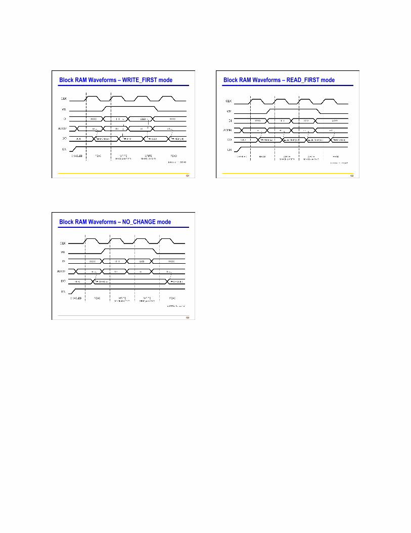
Block RAM with synchronous read (write first mode)
LIBRARY ieee; USE ieee.std_logic_1164.all; USE ieee.std_logic_arith.all;
entity raminfr is generic ( data_bits : integer := 32; -- number of bits per RAM word addr_bits : integer := 3); -- 2^addr_bits = number of words in RAM port (clk : in std_logic; we : in std_logic; a : in std_logic_vector(addr_bits-1 downto 0); di : in std_logic_vector(data_bits-1 downto 0); do : out std_logic_vector(data_bits-1 downto 0)); end raminfr;
94
Block RAM with synchronous read (write first mode) cont'd
architecture behavioral of raminfr is type ram_type is array (2**addr_bits-1 downto 0) of std_logic_vector
(data_bits-1 downto 0); signal RAM : ram_type; signal read_a : std_logic_vector(addr_bits-1 downto 0);
begin process (clk) begin if (clk'event and clk = '1') then if (we = '1') then RAM(conv_integer(unsigned(a))) <= di; end if; read_a <= a;
end if; end process; do <= RAM(conv_integer(unsigned(read_a))); end behavioral;
95
Block RAM Waveforms – WRITE_FIRST mode
96
Report from Synthesis
Resource Usage Report for raminfr Mapping to part: xc3s50pq208-5 Cell usage: GND 1 use RAMB16_S36 1 use VCC 1 use I/O ports: 69 I/O primitives: 68 IBUF 36 uses OBUF 32 uses BUFGP 1 use
I/O Register bits: 0 Register bits not including I/Os: 0 (0%)
RAM/ROM usage summary Block Rams : 1 of 4 (25%) Global Clock Buffers: 1 of 8 (12%)
Mapping Summary: Total LUTs: 0 (0%)
12/8/11
17
97
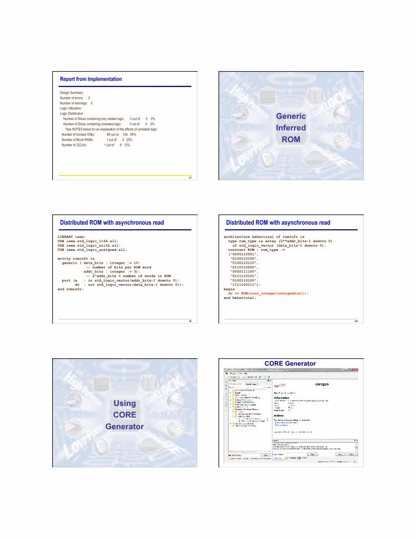
Report from Implementation
Design Summary: Number of errors: 0 Number of warnings: 0 Logic Utilization: Logic Distribution: Number of Slices containing only related logic: 0 out of 0 0% Number of Slices containing unrelated logic: 0 out of 0 0% *See NOTES below for an explanation of the effects of unrelated logic Number of bonded IOBs: 69 out of 124 55% Number of Block RAMs: 1 out of 4 25% Number of GCLKs: 1 out of 8 12%
98
Generic Inferred
ROM
99
Distributed ROM with asynchronous read
LIBRARY ieee; USE ieee.std_logic_1164.all; USE ieee.std_logic_arith.all; USE ieee.std_logic_unsigned.all;
entity rominfr is generic ( data_bits : integer := 10; -- number of bits per ROM word addr_bits : integer := 3); -- 2^addr_bits = number of words in ROM port (a : in std_logic_vector(addr_bits-1 downto 0); do : out std_logic_vector(data_bits-1 downto 0)); end rominfr;
100
Distributed ROM with asynchronous read
architecture behavioral of rominfr is type rom_type is array (2**addr_bits-1 downto 0) of std_logic_vector (data_bits-1 downto 0); constant ROM : rom_type := ("0000110001", "0100110100", "0100110110", "0110110000", "0000111100", "0111110101", "0100110100", "1111100111"); begin do <= ROM(conv_integer(unsigned(a))); end behavioral;
101
Using CORE
Generator
CORE Generator
12/8/11
18
CORE Generator
104
FPGA specific memories
(Instantiation)
105
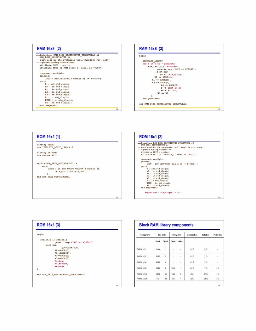
RAM 16x1 (1) library IEEE; use IEEE.STD_LOGIC_1164.all;
library UNISIM; use UNISIM.all;
entity RAM_16X1_DISTRIBUTED is port( CLK : in STD_LOGIC; WE : in STD_LOGIC; ADDR : in STD_LOGIC_VECTOR(3 downto 0); DATA_IN : in STD_LOGIC; DATA_OUT : out STD_LOGIC );
end RAM_16X1_DISTRIBUTED;
106
RAM 16x1 (2) architecture RAM_16X1_DISTRIBUTED_STRUCTURAL of
RAM_16X1_DISTRIBUTED is -- part used by the synthesis tool, Synplify Pro, only; -- ignored during simulation attribute INIT : string; attribute INIT of RAM_16x1s_1: label is "0000”;
component ram16x1s generic( INIT : BIT_VECTOR(15 downto 0) := X"0000"); port( O : out std_ulogic; -- note std_ulogic not std_logic A0 : in std_ulogic; A1 : in std_ulogic; A2 : in std_ulogic; A3 : in std_ulogic; D : in std_ulogic; WCLK : in std_ulogic; WE : in std_ulogic); end component;
107
RAM 16x1 (3)
begin
RAM_16x1s_1: ram16x1s generic map (INIT => X"0000") port map (O => DATA_OUT, A0 => ADDR(0), A1 => ADDR(1), A2 => ADDR(2), A3 => ADDR(3), D => DATA_IN, WCLK => CLK, WE => WE );
end RAM_16X1_DISTRIBUTED_STRUCTURAL;
108
RAM 16x8 (1) library IEEE; use IEEE.STD_LOGIC_1164.all;
library UNISIM; use UNISIM.all;
entity RAM_16X8_DISTRIBUTED is port( CLK : in STD_LOGIC; WE : in STD_LOGIC; ADDR : in STD_LOGIC_VECTOR(3 downto 0); DATA_IN : in STD_LOGIC_VECTOR(7 downto 0); DATA_OUT : out STD_LOGIC_VECTOR(7 downto 0) );
end RAM_16X8_DISTRIBUTED;
12/8/11
19
109
RAM 16x8 (2) architecture RAM_16X8_DISTRIBUTED_STRUCTURAL of
RAM_16X8_DISTRIBUTED is -- part used by the synthesis tool, Synplify Pro, only; -- ignored during simulation attribute INIT : string; attribute INIT of RAM_16x1s_1: label is "0000";
component ram16x1s generic( INIT : BIT_VECTOR(15 downto 0) := X"0000"); port( O : out std_ulogic; A0 : in std_ulogic; A1 : in std_ulogic; A2 : in std_ulogic; A3 : in std_ulogic; D : in std_ulogic; WCLK : in std_ulogic; WE : in std_ulogic); end component;
110
RAM 16x8 (3) begin
GENERATE_MEMORY: for I in 0 to 7 generate RAM_16x1_S_1: ram16x1s generic map (INIT => X"0000") port map (O => DATA_OUT(I), A0 => ADDR(0), A1 => ADDR(1), A2 => ADDR(2), A3 => ADDR(3), D => DATA_IN(I), WCLK => CLK, WE => WE ); end generate;
end RAM_16X8_DISTRIBUTED_STRUCTURAL;
111
ROM 16x1 (1) library IEEE; use IEEE.STD_LOGIC_1164.all;
library UNISIM; use UNISIM.all;
entity ROM_16X1_DISTRIBUTED is port( ADDR : in STD_LOGIC_VECTOR(3 downto 0); DATA_OUT : out STD_LOGIC );
end ROM_16X1_DISTRIBUTED;
112
ROM 16x1 (2) architecture ROM_16X1_DISTRIBUTED_STRUCTURAL of
ROM_16X1_DISTRIBUTED is -- part used by the synthesis tool, Synplify Pro, only; -- ignored during simulation attribute INIT : string; attribute INIT of rom16x1s_1: label is "F0C1";
component ram16x1s generic( INIT : BIT_VECTOR(15 downto 0) := X"0000"); port( O : out std_ulogic; A0 : in std_ulogic; A1 : in std_ulogic; A2 : in std_ulogic; A3 : in std_ulogic; D : in std_ulogic; WCLK : in std_ulogic; WE : in std_ulogic); end component;
signal Low : std_ulogic := '0';
113
ROM 16x1 (3)
begin
rom16x1s_1: ram16x1s generic map (INIT => X"F0C1") port map (O=>DATA_OUT, A0=>ADDR(0), A1=>ADDR(1), A2=>ADDR(2), A3=>ADDR(3), D=>Low, WCLK=>Low, WE=>Low
);
end ROM_16X1_DISTRIBUTED_STRUCTURAL;
114
Block RAM library components
Component Data Cells Parity Cells Address Bus Data Bus Parity Bus
Depth Width Depth Width
RAMB16_S1 16384 1 - - (13:0) (0:0) -
RAMB16_S2 8192 2 - - (12:0) (1:0) -
RAMB16_S4 4096 4 - - (11:0) (3:0) -
RAMB16_S9 2048 8 2048 1 (10:0) (7:0) (0:0)
RAMB16_S18 1024 16 1024 2 (9:0) (15:0) (1:0)
RAMB16_S36 512 32 512 4 (8:0) (31:0) (3:0)
12/8/11
20
115
Component declaration for BRAM (1)
-- Component Declaration for RAMB16_S1 -- Should be placed after architecture statement but before begin component RAMB16_S1 -- synthesis translate_off generic ( INIT : bit_vector := X"0"; INIT_00 : bit_vector := X"0000000000000000000000000000000000000000000000000000000000000000"; ………………………………… INIT_3F : bit_vector := X"0000000000000000000000000000000000000000000000000000000000000000"; SRVAL : bit_vector := X"0"; WRITE_MODE : string := "WRITE_FIRST"); -- synthesis translate_on port (DO : out STD_LOGIC_VECTOR (0 downto 0) ADDR : in STD_LOGIC_VECTOR (13 downto 0); CLK : in STD_ULOGIC; DI : in STD_LOGIC_VECTOR (0 downto 0); EN : in STD_ULOGIC; SSR : in STD_ULOGIC; WE : in STD_ULOGIC); end component;
116
Genaral template of BRAM instantiation (1)
-- Component Attribute Specification for RAMB16_{S1 | S2 | S4} -- Should be placed after architecture declaration but before the begin -- Put attributes, if necessary -- Component Instantiation for RAMB16_{S1 | S2 | S4} -- Should be placed in architecture after the begin keyword RAMB16_{S1 | S2 | S4}_INSTANCE_NAME : RAMB16_S1 -- synthesis translate_off generic map ( INIT => bit_value, INIT_00 => vector_value, INIT_01 => vector_value, …………………………….. INIT_3F => vector_value, SRVAL=> bit_value, WRITE_MODE => user_WRITE_MODE) -- synopsys translate_on port map (DO => user_DO, ADDR => user_ADDR, CLK => user_CLK, DI => user_DI, EN => user_EN, SSR => user_SSR, WE => user_WE);
117
INIT_00 : BIT_VECTOR := X"014A0C0F09170A04076802A800260205002A01C5020A0917006A006800060040"; INIT_01 : BIT_VECTOR := X"000000000000000008000A1907070A1706070A020026014A0C0F03AA09170026"; INIT_02 : BIT_VECTOR := X"0000000000000000000000000000000000000000000000000000000000000000"; INIT_03 : BIT_VECTOR := X"0000000000000000000000000000000000000000000000000000000000000000"; …………………………………………………………………………………………………………………………………… INIT_3F : BIT_VECTOR := X"0000000000000000000000000000000000000000000000000000000000000000")
0000 F0
0000 F1
0000 F2
0000 F3
0000 F4
0000 FE 0000
FF
INIT_3F ADDRESS
0026 10
0917 11
03AA 12
0C0F 13
014A 14
0000 1E
0000 1F
INIT_01 ADDRESS
0040 00
0006 01
0068 02
006A 03
0917 04
0C0F 0E
014A 0F
INIT_00 ADDRESS
Addresses are shown in red and
data corresponding to the same
memory location is shown in black
ADDRESS DATA
Initializing Block RAMs 1024x16
118
Component declaration for BRAM (2)
VHDL Instantiation Template for RAMB16_S9, S18 and S36 -- Component Declaration for RAMB16_{S9 | S18 | S36} component RAMB16_{S9 | S18 | S36} -- synthesis translate_off generic ( INIT : bit_vector := X"0"; INIT_00 : bit_vector :=
X"0000000000000000000000000000000000000000000000000000000000000000"; INIT_3E : bit_vector :=
X"0000000000000000000000000000000000000000000000000000000000000000"; INIT_3F : bit_vector :=
X"0000000000000000000000000000000000000000000000000000000000000000"; INITP_00 : bit_vector :=
X"0000000000000000000000000000000000000000000000000000000000000000"; INITP_07 : bit_vector :=
X"0000000000000000000000000000000000000000000000000000000000000000"; SRVAL : bit_vector := X"0"; WRITE_MODE : string := "WRITE_FIRST"; );
119
Component declaration for BRAM (2)
-- synthesis translate_on port (DO : out STD_LOGIC_VECTOR (0 downto 0); DOP : out STD_LOGIC_VECTOR (1 downto 0); ADDR : in STD_LOGIC_VECTOR (13 downto 0); CLK : in STD_ULOGIC; DI : in STD_LOGIC_VECTOR (0 downto 0); DIP : in STD_LOGIC_VECTOR (0 downto 0); EN : in STD_ULOGIC; SSR : in STD_ULOGIC; WE : in STD_ULOGIC); end component;
120
-- Component Attribute Specification for RAMB16_{S9 | S18 | S36} -- Component Instantiation for RAMB16_{S9 | S18 | S36} -- Should be placed in architecture after the begin keyword RAMB16_{S9 | S18 | S36}_INSTANCE_NAME : RAMB16_S1 -- synthesis translate_off generic map ( INIT => bit_value, INIT_00 => vector_value, . . . . . . . . . . INIT_3F => vector_value, INITP_00 => vector_value, …………… INITP_07 => vector_value SRVAL => bit_value, WRITE_MODE => user_WRITE_MODE) -- synopsys translate_on port map (DO => user_DO, DOP => user_DOP, ADDR => user_ADDR, CLK => user_CLK, DI => user_DI, DIP => user_DIP, EN => user_EN, SSR => user_SSR, WE => user_WE);
Genaral template of BRAM instantiation (2)
12/8/11
21
121
Block RAM Waveforms – WRITE_FIRST mode
122
Block RAM Waveforms – READ_FIRST mode
123
Block RAM Waveforms – NO_CHANGE mode