Embed Size (px)
Citation preview
Review ArticleInAs/GaSb Type-II Superlattice Detectors
Elena A. Plis1,2
1 Center for High Technology Materials, Department of Electrical and Computer Engineering, University of NewMexico, Albuquerque,NM, USA
2 Skinfrared, LLC, Lobo Venture Lab 801, University Boulevard, Suite 10, Albuquerque, NM 87106, USA
Correspondence should be addressed to Elena A. Plis; [email protected]
Received 5 January 2014; Accepted 19 March 2014; Published 10 April 2014
Academic Editor: Meiyong Liao
Copyright © 2014 Elena A. Plis. This is an open access article distributed under the Creative Commons Attribution License, whichpermits unrestricted use, distribution, and reproduction in any medium, provided the original work is properly cited.
InAs/(In,Ga)Sb type-II strained layer superlattices (T2SLs) have made significant progress since they were first proposed as aninfrared (IR) sensing material more than three decades ago. Numerous theoretically predicted advantages that T2SL offers overpresent-day detection technologies, heterojunction engineering capabilities, and technological preferences make T2SL technologypromising candidate for the realization of high performance IR imagers. Despite concentrated efforts of many research groups, theT2SLs have not revealed full potential yet. This paper attempts to provide a comprehensive review of the current status of T2SLdetectors and discusses origins of T2SL device performance degradation, in particular, surface and bulk dark-current components.Various approaches of dark current reduction with their pros and cons are presented.
1. Introduction
Since proposed in 1980s [1–3], the InAs/(In,Ga)Sb T2SLhas gained a lot of interest for the infrared (IR) detectionapplications. Focal plane arrays (FPAs) based on T2SL andoperating in mid-wave IR (MWIR, 3–5 𝜇m) and long-waveIR (LWIR, 8–12𝜇m) are of great importance for a variety ofcivil and military applications. Currently market dominatingtechnologies are based on bulk mercury cadmium telluride(MCT) and InSb [4–6], and GaAs/AlGaAs quantum well IRphotodetectors (QWIPs).
While MCT detectors have very large quantum efficiency(>90%) and detectivity, they are still plagued by nonuniformgrowth defects and a very expensive CdZnTe substrate that isonly available in limited quantities by a foreignmanufacturer.There has been significant progress on development of MCTon silicon substrates, but good performance has been limitedto the MWIR band only. Moreover, MCT is characterizedby low electron effective mass resulting in excessive leakagecurrent [7]. The InSb detectors do not cover the LWIRspectral range. QWIPs are based on III-V semiconductorsand their mature manufacturing process enables them to bescaled to large format FPAs with a high degree of spatialuniformity [8–10]. However, due to polarization selection
rules for electron-photon interactions in GaAs/AlGaAs QW,this material system is insensitive to surface-normal incidentIR radiation resulting in poor conversion quantum efficiency,In addition, their large dark currents lower the operatingtemperature and increase the operating cost of the imager.The development of FPAs based on mature III-V growth andfabrication technology and operating at higher temperatureswill result in highly sensitive, more reliable, lighter, and lesscostly IR sensors than currently available ones.
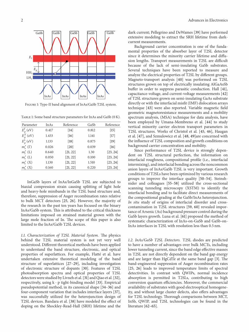
The InAs/(In,Ga)Sb T2SL material system is charac-terized by a broken-gap type-II alignment schematicallyillustrated in Figure 1 with electron and hole wavefunctionshaving maxima in InAs and GaSb layers, respectively. Theoverlap of electron (hole) wave functions between adjacentInAs (GaSb) layers result in the formation of an electron(hole) minibands in the conduction (valence) band. Opticaltransition between the highest hole (heavy-hole) and thelowest conduction minibands is employed for the detectionof incoming IR radiation. The operating wavelength of theT2SLs can be tailored from 3𝜇m to 32 𝜇m by varyingthickness of one or two T2SL constituent layers [11–13]. Someparameters of T2SL constituentmaterials, InAs andGaSb, areshown in Table 1.
Hindawi Publishing CorporationAdvances in ElectronicsVolume 2014, Article ID 246769, 12 pageshttp://dx.doi.org/10.1155/2014/246769
2 Advances in Electronics
GaSb GaSb GaSb GaSb GaSb
InAs InAs InAs InAs
E1
EgHH1
LH1
Figure 1: Type-II band alignment of InAs/GaSb T2SL system.
Table 1: Some band structure parameters for InAs and GaSb (0K).
Parameter InAs Reference GaSb Reference𝐸Γ
𝑔(eV) 0.417 [14] 0.812 [15]𝐸𝑋
𝑔(eV) 1.433 [16] 1.141 [17]𝐸𝐿
𝑔(eV) 1.133 [18] 0.875 [19]𝑚∗
𝑒(Γ) 0.026 [20] 0.039 [16]𝑚∗
𝑙(L) 0.640 [21, 22] 1.30 [23, 24]𝑚∗
𝑡(L) 0.050 [21, 22] 0.100 [23, 24]𝑚∗
𝑙(X) 1.130 [21, 22] 1.510 [23, 24]𝑚∗
𝑡(X) 0.160 [21, 22] 0.220 [23, 24]
InGaSb layers of InAs/InGaSb T2SL are subjected tobiaxial compression strain causing splitting of light holeand heavy-hole minibands in the T2SL band structure and,therefore, suppression of Auger recombination rates relativeto bulk MCT detectors [25, 26]. However, the majority ofthe research in the past ten years has focused on the binaryInAs/GaSb system. This is attributed to the critical thicknesslimitations imposed on strained material grown with thelarge mole fraction of In. The scope of this paper is alsolimited to the InAs/GaSb T2SL devices.
1.1. Characterization of T2SL Material System. The physicsbehind the T2SL material system is not yet very wellunderstood. Different theoretical methods have been appliedto understand the band structure, electronic, and opticalproperties of superlattices. For example, Flatte et al. haveundertaken extensive theoretical modeling of the bandstructure of superlattices [27–29], including investigationof electronic structure of dopants [30]. Features of T2SLphotoabsorption spectra and optical properties of T2SLdetectorswere studied by Livneh et al. [31] andQiao et al. [32],respectively, using k ⋅ p tight-binding model [33]. Empiricalpseudopotential method, in its canonical shape [34–36] andfour-component variation that includes interface layers [37],was successfully utilized for the heterojunction design ofT2SL devices. Bandara et al. [38] have modeled the effect ofdoping on the Shockley-Read-Hall (SRH) lifetime and the
dark current; Pellegrino and DeWames [39] have performedextensive modeling to extract the SRH lifetime from dark-current measurements.
Background carrier concentration is one of the funda-mental properties of the absorber layer of T2SL detectorsince it determines the minority carrier lifetime and diffu-sion lengths. Transport measurements in T2SL are difficultbecause of the lack of semi-insulating GaSb substrates.Several techniques have been reported to measure andanalyze the electrical properties of T2SL by different groups.Magneto-transport analysis [40] was performed on T2SLstructures grown on top of electrically insulating AlGaAsSbbuffer in order to suppress parasitic conduction. Hall [41],capacitance-voltage, and current-voltage measurements [42]of T2SL structures grown on semi-insulating GaAs substratedirectly or with the interfacial misfit (IMF) dislocation arraystechnique [43] were also reported. Variable magnetic fieldgeometric magnetoresistance measurements and a mobilityspectrum analysis, (MSA) technique for data analysis, havebeen employed by Umana-Membreno et al. [44] to studyvertical minority carrier electron transport parameters inT2SL structures. Works of Christol et al. [45, 46], Hauganet al. [47], and Szmulowicz et al. [48, 49]are concerned withthe influence of T2SL composition and growth conditions onbackground carrier concentration and mobility.
Since performance of T2SL device is strongly depen-dent on T2SL structural perfection, the information oninterfacial roughness, compositional profile (i.e., interfacialintermixing), and interfacial bonding across the noncommonanion layers of InAs/GaSb T2SL is very important. Growthconditions of T2SLs have been optimized by various researchgroups to improve the interface quality [50–54]. Steinsh-nider and colleagues [55–58] utilized the cross-sectionalscanning tunneling microscopy (XSTM) to identify theinterfacial bonding and to facilitate direct measurements ofthe compositional grading at the GaSb/InAs heterojunction.In situ study of origins of interfacial disorder and cross-contamination in T2SL structures [59, 60] revealed impor-tance of Arsenic (As) background pressure control during theGaSb layers growth. Luna et al. [61] proposed the method ofsystematic characterization of InAs-on-GaSb and GaSb-on-InAs interfaces in T2SL with resolution less than 0.5 nm.
1.2. InAs/GaSb T2SL Detectors. T2SL diodes are predictedto have a number of advantages over bulk MCTs, includinglower tunneling current, since the band edge effective massesin T2SL are not directly dependent on the band gap energyand are larger than HgCdTe at the same band gap [3]. Theband-engineered suppression of Auger recombination rates[25, 26] leads to improved temperature limits of spectraldetectivities. In contrast with QWIPs, normal incidenceabsorption is permitted in T2SLs, contributing to highconversion quantum efficiencies. Moreover, the commercialavailability of substrates with good electrooptical homogene-ity, and without large cluster defects, also offers advantagesfor T2SL technology. Thorough comparisons between MCT,InSb, QWIP, and T2SL technologies can be found in theliterature [62–65].

Advances in Electronics 3
Table 2: Properties of MWIR and LWIR T2SL detectors at 77 K [88, 89].
Parameter MWIR T2SL 𝜆Cut-off = 5 𝜇m LWIR T2SL 𝜆Cut-off = 10 𝜇mQuantum efficiency (%) ∼70 ∼70𝑅0𝐴 (Ω⋅cm2) 10
6103
Detectivity (Jones) FOV = 0 1 × 10¹⁴
6 × 10¹¹
Table 3: Properties of MWIR and LWIR T2SL FPAs at 77K [90–92].
Parameter MWIR T2SL 𝜆Cut-off = 5𝜇m LWIR T2SL 𝜆Cut-off = 10 𝜇mFormat 320 × 256 1024 × 1024Quantum efficiency (%) ∼50 ∼50NEDT (mK) >15 ∼30
High performance InAs/GaSb T2SL detectors have beenreported for MWIR [66–68], LWIR [12, 69–72], and very-long wave IR (VLWIR) [73, 74] spectral regions. Moreover,mega-pixel FPAs, that is, FPAs of sizes up to 1024 × 1024,have been demonstrated [75, 76]. Multiband T2SL struc-tures were realized, including short-wave IR (SW)/MWIR[77], MW/MWIR [78], MW/LWIR [79, 80], LW/LWIR[81], and SW/MW/LWIR [82] devices. Low-dark-currentarchitectures with unipolar barriers such as M-structure[83], complementary-barrier infrared detector (CBIRD) [70],W-structure [69, 84], N-structure [85], nBn [86, 87], andpBiBn [12] have been designed and fabricated into single-pixel detectors and FPAs at university laboratories (North-western University, Arizona State University, University ofOklahoma, University of Illinois, Georgia Tech University,Bilkent University (Turkey), University of New Mexico),federal laboratories (JPL, NRL, ARL, NVESD, and SNL), andindustrial laboratories (Raytheon, Teledyne Imaging Systems,Hughes Research Laboratories, QmagiQ LLC, etc.). Tables2 and 3 summarize properties of MWIR and LWIR T2SLdetectors and FPAs at 77K.
2. Limitations of T2SL Technology
Despite the numerous technological and theoretically pre-dicted advantages T2SLs offer over present-day detectiontechnologies, the promise of superior performance of T2SLdetectors has not been yet realized. The T2SL detectors areapproaching the empirical benchmark ofMCT’s performancelevel, Rule 07 [93]; however, the dark-current density demon-strated by the T2SL detectors is still significantly higher thanthat of bulkMCT detectors, especially in theMWIR range, asillustrated in Figure 2.
To understand the reasons of high dark-current levelsdemonstrated by the T2SL detectors the origins of dark cur-rent have to be analyzed. Generally, dark current in detectorsbased on narrow band gap semiconductors may be differen-tiated into “bulk” and “surface” currents.Themost important“bulk” dark currents are (i) generation-recombination (G-R) current associated with the SRH process in the depletionregion of the detector and (ii) thermally generated diffusioncurrent associated with Rogalski [94] or radiative process inboth the n- and p-extrinsic regions of the detector [95].
Dar
k-cu
rren
t den
sity
(A/c
m2)
T = 78K10−1
10−2
10−3
10−4
10−5
10−6
10−7
10−8
10−96 7 8 9 10 11 12 13 14
Rule 07IAFJPLNRLNWU
RVSUCSBColumbiaUIUCUNM
Cut-off wavelength (𝜇m)
Figure 2: Dark-current density of T2SL detectors compared withRule 07 [93]. Abbreviations for the different institution working onT2SL detectors: Fraunhofer-Institut (IAF), Jet Propulsion Labora-tory (JPL), Naval Research Laboratory (NRL), Northwestern Uni-versity (NWU), Raytheon Vision Systems (RVS), University of Cal-ifornia, Santa Barbara (UCSB), Columbia University (Columbia),University of Illinois, Urbana-Champaign (UIUC), and Universityof New Mexico (UNM).
The SRH G-R process occurs through the trap levelswithin the energy gap thus limiting lifetime of the minoritycarriers. The origins of SRH centers are not well understood.According to the statistical theory of the SRH process, theSRH rate approaches a maximum as the energy level ofthe trap center approaches midgap. Thus, the most effectiveSRH centers are those located near the middle of the bandgap [96]. Analysis of the defect formation energy of nativedefects dependent on the location of the Fermi level stabiliza-tion energy has been performed by Walukiewicz [97], whoreported that, in bulk GaAs and GaSb, the stabilized Fermilevel is located near either the valence band or the midgap,whereas in bulk InAs the stabilized Fermi level is locatedabove the conduction band edge. From this observation,

4 Advances in Electronics
themidgap trap levels inGaAs andGaSb are available for SRHrecombination, whereas in InAs they are inactive for the SRHprocess, suggesting a longer carrier lifetime in bulk InAs thanin bulk GaSb and GaAs materials. Experimentally measuredvalues of carrier lifetimes yielded ∼325 ns for bulk InAsand ∼100 ns for bulk GaSb, thereby confirming the initialobservation [98]. It may then be hypothesized that nativedefects associated with GaSb are responsible for the SRH-limited minority-carrier lifetimes observed in InAs/GaSbT2SL.
Several methods have been employed to measure life-time of photogenerated carriers of T2SL, including opticalmodulation response [38, 47], time-resolved PL [99–102],andphotoconductive response variationmeasurements [103],to name just a few. Some of them provide more directmeasures of lifetime, while others rely on assumptions orfurther measurements to perform extraction of lifetime [39,104, 105]. Overall, the lifetimes reported forMWIR and LWIRInAs/GaSb T2SL range from 0.13 ns [106] to about 100 ns[107]. These values are significantly lower compared to theMCT devices operating in the same wavelength range [107].
A “surface” dark current component is associated withthe surface states in the junction. During the individual pixelisolation process, the periodic crystal structure terminatesabruptly resulting in formation of unsatisfied (dangling)chemical bonds at the semiconductor-air interface respon-sible for generation of surface states within the band gapand pinning of the Fermi level. Moreover, etch by-products,surface contaminant associated with the fabrication proce-dure, and differential etching also create additional interfacialstates contributing to the dark current. Scaling of the lateraldimensions of a T2SL detector (e.g., typical mesa dimensionsof individual FPA pixels are 20𝜇m × 20𝜇m) makes FPAperformance strongly dependent on surface effects due to alarge pixel surface/volume ratio.
This paper aims to review various ways of improvingperformance of T2SL detectors in order for T2SLs to bethe technology of choice for high-performance IR imagingsystems. Proposed solutions for the reduction of “bulk” and“surface” dark-current components as well as improvementof detector signal-to-noise ratio and operating temperaturelimits will be discussed in detail.
3. Proposed Solutions for the Improvement ofT2SL Detector Performance
3.1. Reduction of “Bulk” Dark Currents. To overcome thecarrier lifetime limitations imposed by the GaSb layerin an InAs/GaSb T2SL, the type-II Ga-free SL, that is,InAs/InAsSb SL, may be utilized for IR detection. A signifi-cantly longer minority carrier lifetime has been obtained inan InAs/InAsSb SL system as compared to an InAs/GaSbT2SL operating in the same wavelength range (at 77K,∼412 ns, and ∼100 ns, resp.) [100, 108]. Such increases inminority carrier lifetimes, along with demonstrated bandgap adjustability [109] and suppressed Auger recombinationrates [110], suggest lower dark currents for InAs/InAsSbSL detectors in comparison with their InAs/GaSb T2SL
counterparts. However, performance, in particular, signal-to-noise ratio, of InAs/InAsSb SL-based detectors with pin[111] and nBn [112] architectures was not superior to T2SL-based devices operating in the same wavelength range. Thismay be attributed to the increased tunneling probability inInAs/InAsSb SL system due to the smaller band offsets [111]and significant concentration of SRH centers in this material[113].
Thermally generated diffusion currents may be signif-icantly suppressed by the incorporation of barriers intoconduction and valence bands to impede the flow of carriersassociated with dark current (noise) without blocking pho-tocurrent (signal). The improved performance of these T2SLdevices is credited to better confinement of the electronwave-functions, reduced tunneling probability, increased electroneffective mass in modified T2SL structures, and reduction indark-current through the use of current blocking layers thatreduce one or more dark-current component. nBn [86, 87],pBiBn [12], M-structure [83], W-structure [84], CBIRD [70],and N-structure [85] are examples of T2SL detectors withbarrier architecture.
The band-offset tunability is critical parameter for therealization of barrier devices. Barrier layers are selected suchthat the hole-blocking layer offers an unimpeded electronsflow while blocking holes and electron-blocking layer fulfillthe opposite function. Hence, one requires hole- (electron)blocking layers to have zero valence (conduction) bandoffsets with the absorber layer. Moreover, for the efficientbarrier structure design, complete macroscopic simulationsare required to get a good assessment of actual dark currentand photocurrent. This simulation may as well help withdesign optimization of barrier structures, in particular, select-ing an optimal barriers thickness, composition, and dopingconcentration.
The extension of concept of heterostructure barrier engi-neering in T2SL resulted in realization of interband cascadeinfrared photodetectors (ICIPs) [114–118]. In ICIP detectorseach cascade stage is comprised of an absorber region,relaxation region, and interband tunneling region. Whilephotocurrent is limited to the value produced in an individualabsorber, adding of extra- stages benefits the signal-to-noiseratio, since the noise current in such devices scales inverselywith the total number of stages. Ability to change numberof stages with different absorber thicknesses is importantfor the design of T2SL detectors with maximized signal-to-noise ratio. The drawbacks of ICIPs are associated with thecomplicated structure of these devices. In particular, due tothe number of layers and interfaces in the structure, someof the fundamental device physics is still unclear and MBEgrowth procedure is challenging.
Ability to heteroengineer the band structure of the T2SLdevices stipulates realization of one more type of low-noiseT2SL detectors, avalanche photodiodes (APDs) [119–121].Control of individual layer thickness and composition offersgreat flexibility in engineering of the electron band structureto initiate single-carrier ionization. Moreover, APDs witheither electron or hole dominated avalanching may be fab-ricated by engineering the higher lying T2SL energy levels.It should be noted that an APD device with hole dominating
Advances in Electronics 5
avalanching is expected to have lower noise due to reducedtunneling of heavier holes. Existence of hole dominatedavalanching structure also opens up possibility of combiningseparate electron and hole multiplication regions in a singledevice achieving very high gain with low excess noise factor.
3.2. Reduction of “Surface” Dark Currents. Despite numerousefforts of various research groups devoted to the developmentof effective passivation schemes for T2SL detectors, there isstill no well-established and generally acknowledged proce-dure for passivation of such devices. Part of the problem isthe complexity of T2SL system, composed by the hundreds ofrelatively thick (several monolayers, MLs) InAs, GaSb, and,sometimes, AlSb layers, and thin (typically, less than 1 ML)interfacial GaAs and InSb layers [55, 57, 58, 122]. Passivationshould satisfy dangling bonds of all these T2SL constituentmaterials, originated at exposed device sidewalls after mesadefinition process, and prevent formation of interface statesin the T2SL band gap.
The great advantage of T2SL system, band gap tun-ability, allowing realization of detectors spanning wide IRrange, serves as a disservice for the passivation development.Interface states cause the pinning of Fermi level with thebands bend towards lower energy near the surface. Thisband bending induces accumulation or type inversion ofcharge resulting in surface tunneling currents along sidewalls.As was shown by Delaunay et al. [123], the narrow bandgap devices (LWIR and VLWIR, with band gap of 120meVor lower) are more susceptible to the formation of chargeconduction channels along the sidewalls. Consequently, thesame passivation may be suitable for the T2SL MWIR andinefficient for the T2SL detectors with longer operatingwavelength.
Moreover, passivation should exhibit thermal and longterm stability. In other words, passivation layer must notundergo any change in its constitutional, physical, andinterfacial properties at variable temperatures (30–300K)during the lifetime of theT2SLdetector (typically, 10,000 hrs).Finally, passivation has to be easily integrated into the FPAfabrication process.
In addition, since passivation applied on rough surfaces,or surfaces contaminated by native oxides, and foreignparticles will result in little or no improvement of deviceperformance, we spent some time discussing the surfacepreparation issues. To achieve minimal surface leakage, thedevice sidewalls must be smooth, with no patterns of prefer-ential etch presented, and clean, with removed native oxidesand etch by-products. Moreover, vertical etch profile is essen-tial for the realization of high-fill factor, small pixel pitch,and large format T2SL FPAs. The thorough comparisons ofvarious surface preparation and passivation techniques ofT2SL detectors are out of the scope of this review article andcan be found in literature [124, 125]. Next two sections aimto familiarize the reader with various mesa definition andpassivation methods developed for T2SL devices.
3.2.1. Surface Preparation. Definition of nearly vertical mesasidewalls that are free of native oxide and defects is the crucial
step in InAs/GaSb T2SL detector fabrication process [126,127]. Presence of elemental antimony on the etched T2SLdevice sidewalls [128] may result in the conduction channelparallel to the interface, which leads to increasing of surfacecomponent of dark current. Unwanted native oxides areusually removed prior to or during the pixel isolation processwith immersion in ammonium sulfide [127], phosphoric orhydrochloric acid based solutions [129]. Introduction of BCl
3
gas into the plasma chemistry is also effective in removal ofnative oxides and redeposited by-products [130].
Nowadays, high-density plasma etch processes are com-monly utilized for InAs/GaSb T2SL material in spite ofinevitable degradation of sidewall surface electronic prop-erties due to ion bombardment or unwanted deposition ofetch by-products [131, 132]. Plasma chemistry usually consistsof chlorine-based precursors (BCl
3, Cl2, or SiCl
2) due to
high volatilities of gallium, indium, antimony, and arsenidechlorides providing fast etch rates and smooth morphologies[133].The resulting etch profiles are vertical due to the plasmasheath and the ionized gas directionality. Damage producedduring the dry etch may be partially restored by subsequentchemical treatment [134]. Due to the ability of wet etchesto cause virtually no surface electronic damage, a chemicaletch attracts attention of researchers for single-pixel T2SLdevice fabrication [135–140]. However, the isotropic natureof wet etch process resulting in concave sidewall profile andan unavoidable tendency to undercut etch masks makingprecise dimensional control more difficult stipulates limitedapplication of wet etches for T2SL FPA fabrication.
3.2.2. Passivation. Conventional passivation methods ofT2SL devices include encapsulation of device sidewalls, bythick layer of dielectric or organic material, and sulfidization.Dielectric passivation of T2SL detectors is compatible withcurrent T2SL FPA fabrication procedures and, consequently,very appealing to the T2SL scientists and engineers. Numer-ous reports on passivation of MWIR and LWIR T2SL detec-tors by silicon oxide or silicon nitride have been publishedover the last fifteen years [74, 81, 130, 141–144]. Dielectric pas-sivation, though shown to be effective, presents the challengesof developing high-quality, low fixed, and interfacial chargesdensity dielectrics at process temperatures substantially lowerthat the InAs/GaSb T2SL growth temperature to preventthe T2SL period intermixing. Moreover, native fixed chargespresented in dielectric passivation layer can either improveor deteriorate the device performance [143]; consequently,the dielectric passivation may not passivate the low band gapmaterials as effectively as high band gap materials.
T2SL passivation with organic materials, which are poly-imide or various photoresists (PRs), is emerging alternativeto the dielectric passivation approach [134, 135, 145–150]. PRsare commonly deposited at room temperature and thus theT2SL thermal budget is not exerted. Moreover, PRs equallyeffectively passivate T2SL detectors with different operatingwavelengths.
Chalcogenide passivation, or saturation of unsatisfiedbonds on semiconductor surface by sulfur atoms, has beenemployed from early 1990s for the passivation of bulk III-V
6 Advances in Electronics
materials [151–162]. The enhanced photoluminescence (PL)and reduced diode leakage current were credited to theformation of III-S bond responsible for the reduction ofsurface states within band gap.
The simplest sulfidization scheme of T2SL detectors isdevice immersion in aqueous solution of ammonium sulfide.No native oxide removal step is required prior to passivationbecause the native oxides are etched by (NH
4)OH formed
in water solution of ammonium sulfide. Short-term benefitsfor the MWIR and LWIR T2SL device performance havebeen reported [127, 129, 163] and the necessity for a suitablecapping layer to preserve good passivation quality in thelong term was reaffirmed. Thioacetamide (TAM, C
2H5NS)
[124, 164] and octadecanethiol (ODT, CH3[CH2]17SH) [85]
treatments offer formation of more stable bonds betweensulfur and T2SL constituent elements (Ga, In, As, and Sb)compared to weaker III (V)-oxygen-S bonds formed afterammonium sulfide treatment.
One of relatively new sulfidization methods is electro-chemical passivation (ECP) [129, 165] that is saturationof dangling bonds with sulfur through electrolysis in S-containing solution. Though effective, sulfur layer depositedthrough ECP may oxidize easily and additional encapsula-tion is required. Electron-beam evaporated ZnS satisfies thedangling bonds with S-atoms simultaneously acting as anencapsulant [119–121, 166].
Recently, several research groups reported the “com-bined” approach for the passivation of T2SL detectors. Forexample, Zhang et al. [167] noticed that the anodic sulfidepassivation combined with the SiO
2significantly improved
the performance of MWIR T2SL detectors. DeCuir Jr. et al.[147] found that the sulfide chemical treatment followed bythe SU-8 treatment inhibits the formation of native surfaceoxides, satisfies dangling bonds, and prevents the sulfide layerdegradation over time.
4. Other Methods of T2SL DetectorPerformance Improvement
The bulk components of the dark current (SRH and ther-mally generated diffusion current) in T2SL detector may besignificantly diminished by scaling thickness of the device.The abridged quantum efficiency (QE) of such device may berestored through plasmon assisted coupling of incident elec-tromagnetic radiation while maintaining low dark-currentlevel. Transmission enhancement and QE increase throughsubwavelength metal hole array [168] and corrugated metalsurface structure [169], respectively, have been reported forMWIR T2SL detectors.
Surface currents may be suppressed by reduced exposureof narrow gapmaterials to the environment, for example, as aresult of encapsulation of etched sidewalls withwide band gapmaterial [133, 170] or buried architecture [84] that isolates theneighboring devices but terminates within a wider band gaplayer. The former passivation approach requires very carefulsurface cleaning prior the overgrowth procedure, whereaslatter is subjected to the possible crosstalk issues in FPAs dueto the uncertainty of the lateral diffusion length of minority
carriers. If the values of lateral diffusion length are larger thanthe distance between neighboring pixels in the FPA, crosstalkbetween the FPA elements can be encountered that leads tothe degradation of image resolution.
Another approach for the realization of high performanceT2SL sensors is growth of T2SL structures on high-indexplane GaSb [171]. The thickness of the T2SL detector grownon the GaSb (111) substrate is reduced due to the natural dif-ference of lattice parameters in the (111) and (100) directions,whereas heavy hole confinement is increased by a factor ofthree [172]. This translates into thinner detector structuresfor a given detection wavelength and absorption coefficientrealized on (111) GaSb substrate, resulting in shorter growthtimes. This also means decreased costs and material usage,both of which are highly desirable. Moreover, the decreaseddetector volume results in an improved signal-to-noise ratio,since the number of thermally generated carriers is corre-spondingly reduced.
5. Summary
This work provides a review of the current status and limita-tions of IR detectors based on an InAs/GaSb T2SLs. It shouldbe noted that applications of T2SL system are not limitedto the IR detection only. Low thermal conductivity of T2SLidentifies it as a prospective material for low-temperaturePeltier coolers [173]. Spatially separated confinement ofelectrons and holes, signature of type-II band alignment,initiated InAs/GaSb core-shell nanowires realization [174,175]. Field-effect transistors (FETs) [176, 177] and thermophotovoltaic (TPV) [178] T2SL devices are another examplesof unconventional applications of T2SL material system.
Despite the numerous theoretically predicted advantagesthat T2SLs offer over MCT, InSb, and QWIP-based detectors,intensive heterostructure engineering efforts and develop-ment of epitaxial growth and fabrication techniques, thepromise of superior performance of T2SL detectors has notbeen yet realized. The dark-current density demonstrated bythe T2SL detectors is still significantly higher than that of bulkMCT detectors, especially in the MWIR range.
The complexity of T2SL system, along with the intricatedetector architectures, results in no universal solution forthe suppression of dark currents. Different approaches thataddress suppression of either bulk or surface dark currentcomponents in order for T2SL to be the technology of choicefor high-performance imaging systems have been presented.
The SRH and thermally generated diffusion currents maybe significantly reduced by exclusion of GaSb layer fromInAs/GaSb T2SL stack, that is, Ga-free T2SL, and by theincorporation of barriers device structure to impede theflow of carriers associated with dark current (noise) with-out blocking photocurrent (signal), respectively. Passivationtreatment of the exposed device sidewalls decreases the sur-face currents. However, development of effective passivationtechnique is hindered by the ease of native oxide formationand requirements to the etched surface. In addition, thesame passivation may be suitable for the T2SL MWIR andinefficient for the T2SL detectors with longer operating
Advances in Electronics 7
wavelength. Finally, one of the most effective passivationapproaches, saturation of unsatisfied chemical bonds withsulfur atoms, results in formation of passivation layer withpoor long-term stability, and additional encapsulation isrequired.
Integration of T2SL detectors with surface plasmon cou-plers and utilization of high-index plane GaSb substrates arerecent alternatives for the improvement of T2SL detectorperformance.Despite the promising preliminary results, bothof these directions require additional investigation.
In conclusion, unique combination of band structureengineering flexibility and material properties of InAs/GaSbT2SL provide a prospective benefit in the realization ofnext generation IR imagers. Performance of MWIR andLWIR T2SL detectors has not achieved its theoreticallypredicted limit. To fully realize the T2SL potential methodsof suppression of various dark current components have tobe developed. Up-to-date techniques of dark current reduc-tion include not only traditional passivation, but advancedheterostructure engineering and integration of T2SL withnanostructures as well.
Conflict of Interests
The author declares that there is no conflict of interestsregarding the publication of this paper.
Acknowledgments
This work was supported by the AFOSR FA9550-10-1-0113and AFRL FA9453-12-1-0336 Grants.
References
[1] G. A. Sai-Halasz, R. Tsu, and L. Esaki, “A new semiconductorsuperlattice,”Applied Physics Letters, vol. 30, no. 12, pp. 651–653,1977.
[2] L. Esaki, “InAs-GaSb superlattices-synthesized semiconductorsand semimetals,” Journal of Crystal Growth, vol. 52, no. 1, pp.227–240, 1981.
[3] D. L. Smith and C. Mailhiot, “Proposal for strained type IIsuperlattice infrared detectors,” Journal of Applied Physics, vol.62, no. 6, pp. 2545–2548, 1987.
[4] J. Rothman, E. D. Borniol, P. Ballet et al., “HgCdTe APD-Focalplane array performance at DEFIR,” in Infrared Technologyand Applications XXXV, vol. 7298 of Proceedings of SPIE, pp.729835–729845, April 2009.
[5] J.M. Peterson,D.D. Lofgreen, J. A. Franklin et al., “MBE growthof HgCdTe on large-area Si and CdZnTe wafers for SWIR,MWIR and LWIR detection,” Journal of Electronic Materials,vol. 37, no. 9, pp. 1274–1282, 2008.
[6] O. Nesher, I. Pivnik, E. Ilan et al., “High resolution 1280×1024,15 𝜇m pitch compact InSb IR detector with on-chip ADC,”in Infrared Technology and Applications XXXV, vol. 7298 ofProceedings of SPIE, April 2009.
[7] A. Rogalski, “HgCdTe infrared detector material: history, statusand outlook,” Reports on Progress in Physics, vol. 68, no. 10, pp.2267–2336, 2005.
[8] H. Schneider and H. C. Liu,QuantumWell Infrared Photodetec-tors, Springer Series in Optical Sciences, Springer, 2007.
[9] A. Soibel, S. V. Bandara, D. Z. Ting et al., “A super-pixel QWIPfocal plane array for imaging multiple waveband temperaturesensor,” Infrared Physics and Technology, vol. 52, no. 6, pp. 403–407, 2009.
[10] A. Nedelcu, V. Gueriaux, A. Bazin et al., “Enhanced quantumwell infrared photodetector focal plane arrays for space appli-cations,” Infrared Physics and Technology, vol. 52, no. 6, pp. 412–418, 2009.
[11] C. Cervera, I. Ribet-Mohamed, R. Taalat, J. P. Perez, P. Christol,and J. B. Rodriguez, “Dark current and noise measurementsof an InAs/GaSb superlattice photodiode operating in themidwave infrared domain,” Journal of Electronic Materials, vol.41, pp. 2714–2718, 2012.
[12] N. Gautam, H. S. Kim, M. N. Kutty, E. Plis, L. R. Dawson, andS. Krishna, “Performance improvement of longwave infraredphotodetector based on type-II InAs/GaSb superlattices usingunipolar current blocking layers,” Applied Physics Letters, vol.96, no. 23, Article ID 231107, 2010.
[13] Y. Wei, A. Gin, M. Razeghi, and G. J. Brown, “AdvancedInAs/GaSb superlattice photovoltaic detectors for very longwavelength infrared applications,” Applied Physics Letters, vol.80, no. 18, pp. 3262–3264, 2002.
[14] Y. Lacroix, C. A. Tran, S. P. Watkins, and M. L. W. Thewalt,“Low-temperature photoluminescence of epitaxial InAs,” Jour-nal of Applied Physics, vol. 80, no. 11, pp. 6416–6424, 1996.
[15] P. S. Dutta, H. L. Bhat, and V. Kumar, “The physics andtechnology of gallium antimonide: an emerging optoelectronicmaterial,” Journal of Applied Physics, vol. 81, no. 9, pp. 5821–5870,1997.
[16] M. Levinshtein, S. Rumyantsev, and M. Shur, Eds., HandbookSeries on Semiconductor Parameters, vol. 1 and 2, World Scien-tific, 1996.
[17] A. Joullie, A. Z. Eddin, and B. Girault, “Temperature depen-dence of the 𝐿𝑐
6−Γ𝑐
6energy gap in gallium antimonide,” Physical
Review B, vol. 23, no. 2, pp. 928–930, 1981.[18] E. Adachi, “Energy band parameters of InAs at various temper-
atures,” Journal of the Physical Society of Japan, vol. 24, no. 5, p.1178, 1968.
[19] C. Alibert, A. Joullie, and A. M. Joullie, “Modulation-spectroscopy study of the GaAlSb band structure,” PhysicalReview B, vol. 27, p. 4946, 1983.
[20] M. B. Thomas and J. C. Woolley, “Plasma edge reflectancemeasurements in GaInAs and InAsSb alloys,” Canadian Journalof Physics, vol. 49, p. 2052, 1971.
[21] D. C. Tsui, “Landau-level spectra of conduction electrons at anInAs surface,” Physical Review B, vol. 12, no. 12, pp. 5739–5748,1975.
[22] R. A. Stradling and R. A. Wood, “The temperature dependenceof the band-edge effective masses of InSb, InAs and GaAsas deduced from magnetophonon magnetoresistance measure-ments,” Journal of Physics C: Solid State Physics, vol. 3, no. 5,article 005, pp. L94–L99, 1970.
[23] C. Ghezzi, R. Magnanini, A. Parisini et al., “Optical absorptionnear the fundamental absorption edge inGaSb,”Physical ReviewB, vol. 52, no. 3, pp. 1463–1466, 1995.
[24] H. Arimoto, N. Miura, R. J. Nicholas, N. J. Mason, and P.J. Walker, “High-field cyclotron resonance in the conductionbands of GaSb and effective-mass parameters at the L points,”Physical Review B, vol. 58, no. 8, pp. 4560–4565, 1998.
[25] E. R. Youngdale, J. R. Meyer, C. A. Hoffman et al., “Auger life-time enhancement in InAs-Ga
1−𝑥In𝑥Sb superlattices,” Applied
Physics Letters, vol. 64, no. 23, pp. 3160–3162, 1994.
8 Advances in Electronics
[26] G. M. Williams, “Comment on “Temperature limits oninfrared detectivities of InAs/In
𝑥Ga1−𝑥
Sb superlattices and bulkHg𝑥Cd1−𝑥
Te” [J. Appl. Phys. 74, 4774 (1993)],” Journal of AppliedPhysics, vol. 77, no. 8, pp. 4153–4155, 1995.
[27] M. E. Flatte, C. H. Grein, H. Ehrenreich, R. H. Miles,and H. Cruz, “Theoretical performance limits of 2.1-4.1𝜇mInAs/InGaSb,HgCdTe, and InGaAsSb lasers,” Journal of AppliedPhysics, vol. 78, no. 7, pp. 4552–4561, 1995.
[28] K. Abu El-Rub, C. H. Grein, M. E. Flatte, and H. Ehrenreich,“Band structure engineering of superlattice-based short-, mid-,and long-wavelength infrared avalanche photodiodes forimproved impact ionization rates,” Journal of Applied Physics,vol. 92, no. 7, pp. 3771–3778, 2002.
[29] M. E. Flatte and C. H. Grein, “Theory and modeling of type-II strained-layer superlattice detectors,” in Quantum Sensingand Nanophotonic Devices VI, vol. 7222 of Proceedings of SPIE,January 2009.
[30] M. E. Flatte and C. E. Pryor, “Defect states in type-II strained-layer superlattices,” in Quantum Sensing and NanophotonicDevices VII, vol. 7608 of Proceedings of SPIE, January 2010.
[31] Y. Livneh, P. Klipstein, O. Klin et al., “kp model for theenergy dispersions and absorption spectra of InAs/GaSb type-IIsuperlattices,” Physical Review B, vol. 86, Article ID 235311, 2012.
[32] P.-F. Qiao, S. Mou, and S. L. Chuang, “Electronic band struc-tures and optical properties of type-II superlattice photodetec-tors with interfacial effect,” Optics Express, vol. 20, no. 3, pp.2319–2334, 2013.
[33] P. C. Klipstein, “Operator ordering and interface-band mixingin theKane-likeHamiltonian of lattice-matched semiconductorsuperlattices with abrupt interfaces,” Physical Review B, vol. 81,no. 23, Article ID 235314, 2010.
[34] G. C. Dente and M. L. Tilton, “Pseudopotential methodsfor superlattices: applications to mid-infrared semiconductorlasers,” Journal of Applied Physics, vol. 86, no. 3, pp. 1420–1429,1999.
[35] R. Kaspi, C. Moeller, A. Ongstad et al., “Absorbance spec-troscopy and identification of valence subband transitions intype-II InAs/GaSb superlattices,”Applied Physics Letters, vol. 76,no. 4, pp. 409–411, 2000.
[36] G. C. Dente and M. L. Tilton, “Comparing pseudopotentialpredictions for InAs/GaSb superlattices,” Physical Review B, vol.66, no. 16, Article ID 165307, 2002.
[37] J. M. Masur, R. Rehm, J. Schmitz, L. Kirste, and M.Walther, “Four-component superlattice empirical pseudopo-tential method for InAs/GaSb superlattices,” Infrared Physics &Technology, vol. 61, pp. 129–133, 2013.
[38] S. Bandara, P. G. Maloney, N. Baril, J. G. Pellegrino, and M.Z. Tidrow, “Doping dependence of minority carrier lifetimein long-wave Sb-based type II superlattice infrared detectormaterials,”Optical Engineering, vol. 50, no. 6, Article ID 061015,2011.
[39] J. Pellegrino and R. DeWames, “Minority carrier lifetimecharacteristics in type II InAs/GaSb LWIR superlattice n+𝜋p+photodiodes,” in Infrared Technology and Applications XXXV,vol. 7298 of Proceedings of SPIE, April 2009.
[40] L. Burkle, F. Fuchs, J. Schmitz, and W. Pletschen, “Control ofthe residual doping of InAs/(GaIn)Sb infrared superlattices,”Applied Physics Letters, vol. 77, no. 11, pp. 1659–1661, 2000.
[41] X. B. Zhang, J. H. Ryou, R. D. Dupuis et al., “Improved surfaceand structural properties of InAs/GaSb superlattices on (001)GaSb substrate by introducing an InAsSb layer at interfaces,”Applied Physics Letters, vol. 90, no. 13, Article ID 131110, 2007.
[42] X. B. Zhang, J. H. Ryou, R. D. Dupuis et al., “Metalorganicchemical vapor deposition growth of high-quality InAsGaSbtype II superlattices on (001) GaAs substrates,” Applied PhysicsLetters, vol. 88, no. 7, Article ID 072104, 2006.
[43] A. Jallipalli, G. Balakrishnan, S. H. Huang et al., “Structuralanalysis of highly relaxed GaSb grown on GaAs substrates withperiodic interfacial array of 90∘ misfit dislocations,” NanoscaleResearch Letters, vol. 4, no. 12, pp. 1458–1462, 2009.
[44] G. Umana-Membreno, B. Klein, H. Kala et al., “Verticalminority carrier electron transport in p-type InAs/GaSb type-IIsuperlattices,” Applied Physics Letters, vol. 101, no. 25, Article ID253515, 2012.
[45] P. Christol, L. Konczewicz, Y. Cuminal, H. Aıt-Kaci, J. B.Rodriguez, and A. Joullie, “Electrical properties of short periodInAs/GaSb superlattice,” Physica Status Solidi C, vol. 4, no. 4, pp.1494–1498, 2007.
[46] C. Cervera, J. B. Rodriguez, J. P. Perez et al., “Unambigu-ous determination of carrier concentration and mobility forInAs/GaSb superlattice photodiode optimization,” Journal ofApplied Physics, vol. 106, no. 3, Article ID 033709, 2009.
[47] H. J. Haugan, S. Elhamri, F. Szmulowicz, B. Ullrich, G. J. Brown,and W. C. Mitchel, “Study of residual background carriersin midinfrared InAsGaSb superlattices for unfcooled detectoroperation,” Applied Physics Letters, vol. 92, no. 7, Article ID071102, 2008.
[48] F. Szmulowicz, S. Elhamri, H. J. Haugan, G. J. Brown, andW. C.Mitchel, “Demonstration of interface-scattering-limited elec-tron mobilities in InAs/GaSb superlattices,” Journal of AppliedPhysics, vol. 101, no. 4, Article ID 043706, 2007.
[49] F. Szmulowicz, S. Elhamri, H. J. Haugan, G. J. Brown, and W.C. Mitchel, “Carrier mobility as a function of carrier densityin type-II InAs/GaSb superlattices,” Applied Physics Letters, vol.105, Article ID 074303, 2009.
[50] K. Mahalingam, H. J. Haugan, G. J. Brown, and A. J.Aronow, “Strain analysis of compositionally tailored interfacesin InAs/GaSb superlattices,”Applied Physics Letters, vol. 103, no.21, Article ID 211605, 2013.
[51] H. Kim, Y.Meng, J. L. Rouviere, D. Isheim,D.N. Seidman, and J.M. Zuo, “Atomic resolution mapping of interfacial intermixingand segregation in InAs/GaSb superlattices: a correlative study,”Journal of Applied Physics, vol. 113, no. 10, Article ID 103511, 2013.
[52] Z. Xu, J. Chen, F. Wang, Y. Zhou, C. Jin, and L. He, “Interfacelayer control and optimization of InAs/GaSb type-II super-lattices grown by molecular beam epitaxy,” Journal of CrystalGrowth, vol. 386, pp. 220–225, 2014.
[53] B. Arikan, G. Korkmaz, Y. E. Suyolcu, B. Aslan, andU. Serincan,“On the structural characterization of InAs/GaSb type-II super-lattices: the effect of interfaces for fixed layer thicknesses,”ThinSolid Films, vol. 548, pp. 288–291, 2013.
[54] Y. Ashuach, Y. Kauffmann, C. Saguy et al., “Quantification ofatomic intermixing in short-period InAs/GaSb superlattices forinfrared photodetectors,” Journal of Applied Physics, vol. 113, no.18, Article ID 184305, 2013.
[55] J. Steinshnider, M. Weimer, R. Kaspi, and G. W. Turner,“Visualizing interfacial structure at non-common-atom hetero-junctions with cross-sectional scanning tunneling microscopy,”Physical Review Letters, vol. 85, no. 14, pp. 2953–2956, 2000.
[56] J. Steinshnider, J. Harper, M. Weimer, C.-H. Lin, S. S. Pei, andD. H. Chow, “Origin of antimony segregation in GaInSb/InAsstrained-layer superlattices,” Physical Review Letters, vol. 85, no.21, pp. 4562–4565, 2000.
Advances in Electronics 9
[57] R. Kaspi, J. Steinshnider, M. Weimer, C. Moeller, and A.Ongstad, “As-soak control of the InAs-on-GaSb interface,”Journal of Crystal Growth, vol. 225, no. 2–4, pp. 544–549, 2001.
[58] R. Kaspi, “Compositional abruptness at the InAs-on-GaSbinterface: optimizing growth by using the Sb desorption signa-ture,” Journal of Crystal Growth, vol. 201-202, pp. 864–867, 1999.
[59] P. M. Thibado, B. R. Bennett, M. E. Twigg, B. V. Shanabrook,andL. J.Whitman, “Origins of interfacial disorder inGaSb/InAssuperlattices,” Applied Physics Letters, vol. 67, pp. 3578–3580,1995.
[60] E. M. Jackson, G. I. Boishin, E. H. Aifer, B. R. Bennett, andL. J. Whitman, “Arsenic cross-contamination in GaSb/InAssuperlattices,” Journal of Crystal Growth, vol. 270, no. 3-4, pp.301–308, 2004.
[61] E. Luna, B. Satpati, J. B. Rodriguez, A. N. Baranov, E. Tournı,and A. Trampert, “Interfacial intermixing in InAs/GaSb short-period-superlattices grown bymolecular beam epitaxy,”AppliedPhysics Letters, vol. 96, no. 2, Article ID 021904, 2010.
[62] M. A. Kinch, “Fundamental physics of infrared detector mate-rials,” Journal of Electronic Materials, vol. 29, no. 6, pp. 809–817,2000.
[63] A. Rogalski, “Third-generation infrared photon detectors,”Optical Engineering, vol. 42, no. 12, pp. 3498–3516, 2003.
[64] A. Rogalski, “Infrared detectors: status and trends,” Progress inQuantum Electronics, vol. 27, no. 2-3, pp. 59–210, 2003.
[65] C. Downs and T. E. Vanderveld, “Progress in infrared photode-tectors since 2000,” Sensors, vol. 13, pp. 5054–5098, 2013.
[66] M. Walther, J. Schmitz, R. Rehm et al., “Growth of InAs/GaSbshort-period superlattices for high-resolution mid-wavelengthinfrared focal plane array detectors,” Journal of Crystal Growth,vol. 278, no. 1–4, pp. 156–161, 2005.
[67] Y. Wei, A. Hood, H. Yau et al., “Uncooled operation of type-II InAs/GaSb superlattice photodiodes in the midwavelengthinfrared range,” Applied Physics Letters, vol. 86, no. 23, ArticleID 233106, pp. 1–3, 2005.
[68] E. Plis, J. B. Rodriguez, H. S. Kim et al., “Type II InAsGaSbstrain layer superlattice detectors with p-on-n polarity,”AppliedPhysics Letters, vol. 91, no. 13, Article ID 133512, 2007.
[69] I. Vurgaftman, E. H. Aifer, C. L. Canedy et al., “Graded bandgap for dark-current suppression in long-wave infrared W-structured type-II superlattice photodiodes,” Applied PhysicsLetters, vol. 89, no. 12, Article ID 121114, 2006.
[70] D. Z.-Y. Ting, C. J. Hill, A. Soibel et al., “A high-performancelong wavelength superlattice complementary barrier infrareddetector,” Applied Physics Letters, vol. 95, no. 2, Article ID023508, 2009.
[71] P. Y. Delaunay andM. Razeghi, “Spatial noise and correctabilityof type-II InAs/GaSb focal plane arrays,” IEEE Journal ofQuantum Electronics, vol. 46, no. 4, pp. 584–588, 2010.
[72] N. Gautam, S. Myers, A. V. Barve et al., “Barrier engineeredinfrared photodetectors based on type-II InAs/GaSb strainedlayer superlattices,” IEEE Journal of Quantum Electronics, vol.49, no. 2, pp. 211–217, 2013.
[73] Y. Wei, A. Gin, M. Razeghi, and G. J. Brown, “Type IIInAs/GaSb superlattice photovoltaic detectors with cutoffwave-length approaching 32 𝜇m,” Applied Physics Letters, vol. 81, no.19, pp. 3675–3677, 2002.
[74] A. Hood, M. Razeghi, E. H. Aifer, and G. J. Brown, “On the per-formance and surface passivation of type II InAs/GaSb super-lattice photodiodes for the very-long-wavelength infrared,”Applied Physics Letters, vol. 87, no. 15, Article ID 151113, pp. 1–3, 2005.
[75] S. D. Gunapala, D. Z. Ting, C. J. Hill et al., “Demonstration of a1024 × 1024 Pixel InAsGaSb superlattice focal plane array,” IEEEPhotonics Technology Letters, vol. 22, no. 24, pp. 1856–1858, 2010.
[76] A. Haddadi, S. Ramezani-Darvish, G. Chen, A. M. Hoang, B.-M. Nguyen, andM. Razeghi, “High operability 1024 × 1024 longwavelength type-II superlattice focal plane array,” IEEE Journalof Quantum Electronics, vol. 48, no. 2, pp. 221–228, 2012.
[77] A. M. Hoang, G. Chen, A. Haddadi, and M. Razeghi, “Demon-stration of high-performance biasselectable dual-band short-mid-wavelength infrared photodetectors based on type-IIInAs/GaSb/AlSb superlattices,” Applied Physics Letters, vol. 102,Article ID 011108, 2013.
[78] R. Rehm, M. Walther, F. Rutz et al., “Dual-color InAs/GaSbsuperlattice focal-plane array technology,” Journal of ElectronicMaterials, vol. 40, no. 8, pp. 1738–1743, 2011.
[79] A. Khoshakhlagh, J. B. Rodriguez, E. Plis et al., “Bias dependentdual band response from InAsGa (In) Sb type II strain layersuperlattice detectors,” Applied Physics Letters, vol. 91, no. 26,Article ID 263504, 2007.
[80] E. Plis, S. S. Krishna, E. P. Smith, S. Johnson, and S. Krishna,“Voltage controllable dual-band response from InAs/GaSbstrained layer superlattice detectors with nBn design,” Electron-ics Letters, vol. 47, no. 2, pp. 133–134, 2011.
[81] J. Huang, W. Ma, C. Cao et al., “Mid wavelength type IIInAs/GaSb superlattice photodetector using SiO
𝑥N𝑦passiva-
tion,” Japanese Journal of Applied Physics, vol. 51, Article ID074002, 2012.
[82] N. Gautam,M.Naydenkov, S.Myers et al., “Three color infrareddetector using InAs/GaSb superlattices with unipolar barriers,”Applied Physics Letters, vol. 98, no. 12, Article ID 121106, 2011.
[83] B.-M. Nguyen, D. Hoffman, P.-Y. Delaunay, and M. Razeghi,“Dark current suppression in type II InAsGaSb superlattice longwavelength infrared photodiodes with M-structure barrier,”Applied Physics Letters, vol. 91, no. 16, Article ID 163511, 2007.
[84] E. H. Aifer, J. H.Warner, C. L. Canedy et al., “Shallow-etchmesaisolation of graded-bandgap W-structured type II superlatticephotodiodes,” Journal of Electronic Materials, vol. 39, pp. 1070–1079, 2010.
[85] O. Salihoglu, A. Muti, K. Kutluer et al., “N-structure for type-II superlattice photodetectors,” Applied Physics Letters, vol. 101,no. 7, Article ID 073505, 2012.
[86] J. B. Rodriguez, E. Plis, G. Bishop et al., “NBn structure based onInAs/GaSb type-II strained layer superlattices,” Applied PhysicsLetters, vol. 91, no. 4, Article ID 043514, 2008.
[87] H. S. Kim, E. Plis, J. B. Rodriguez et al., “Mid-IR focal plane arraybased on type-II InAsGaSb strain layer superlattice detectorwith nBn design,” Applied Physics Letters, vol. 92, no. 18, ArticleID 183502, 2008.
[88] A. Rogalski, J. Antoszewski, and L. Faraone, “Third-generationinfrared photodetector arrays,” Journal of Applied Physics, vol.105, no. 9, Article ID 091101, 2009.
[89] A. Rogalski, “Progress in focal plane array technologies,”Progress in Quantum Electronics, vol. 36, p. 342, 2012.
[90] M. Sundaram, A. Reisinger, R. Dennis et al., “Evolution ofarray format of longwave infrared Type-II SLS FPAs with highquantum efficiency,” Infrared Physics & Technology, vol. 59, pp.12–17, 2013.
[91] M. Razeghi, A. Haddadi, A. Hoang et al., “Advances inantimonide-based Type-II superlattices for infrared detectionand imaging at center for quantum devices,” Infrared Physics &Technology, vol. 59, pp. 41–52, 2013.
10 Advances in Electronics
[92] D. Z. Ting, A. Soibel, S. A. Keo et al., “Development ofquantum well, quantum dot, and type II superlattice infraredphotodetectors,” Journal of Applied Remote Sensing, vol. 8,Article ID 084998, 2014.
[93] D. R. Rhiger, “Performance comparison of long-wavelengthinfrared type II superlattice devices with HgCdTe,” Journal ofElectronic Materials, vol. 40, no. 8, pp. 1815–1822, 2011.
[94] A. Rogalski, New Ternary Alloy Systems for Infrared Detectors,SPIE, Bellingham, Wash, USA, 1994.
[95] S.Maimon andG.W.Wicks, “nBn detector, an infrared detectorwith reduced dark current and higher operating temperature,”Applied Physics Letters, vol. 89, no. 15, Article ID 151109, 2006.
[96] W. Shockley and J. W. T. Read, “Statistics of the recombinationsof holes and electrons,” Physical Review, vol. 87, no. 5, pp. 835–842, 1952.
[97] W.Walukiewicz, “Defect reactions at metal-semiconductor andsemiconductor-semiconductor interfaces,” Materials ResearchSociety Symposium Proceedings, vol. 148, p. 137, 1989.
[98] S. P. Svensson, D. Donetsky, D.Wang, H. Hier, F. J. Crowne, andG. Belenky, “Growth of type II strained layer superlattice, bulkInAs andGaSbmaterials forminority lifetime characterization,”Journal of Crystal Growth, vol. 334, no. 1, pp. 103–107, 2011.
[99] B. C. Connelly, G. D. Metcalfe, H. Shen, and M. Wraback,“Direct minority carrier lifetime measurements and recombi-nation mechanisms in long-wave infrared type II superlatticesusing time-resolved photoluminescence,” Applied Physics Let-ters, vol. 97, no. 25, Article ID 251117, 2010.
[100] E. H. Steenbergen, B. C. Connelly, G. D. Metcalfe et al.,“Significantly improved minority carrier lifetime observed in along-wavelength infrared III-V type-II superlattice comprisedof InAs/InAsSb,” Applied Physics Letters, vol. 99, no. 25, ArticleID 251110, 2011.
[101] G. Belenky, G. Kipshidze, D. Donetsky et al., “Effects of carrierconcentration and phonon energy on carrier lifetime in Type-2SLS and properties of InAs
1−𝑋Sb𝑋alloys,” in Infrared Technology
and Applications XXXVII, vol. 8012 of Proceedings of SPIE, April2011.
[102] L. Murray, K. Lokovic, B. Olson, A. Yildirim, T. Boggess, andJ. Prineas, “Effects of growth rate variations on carrier lifetimeand interface structure in InAs/GaSb superlattices,” Journal ofCrystal Growth, vol. 386, pp. 194–198, 2014.
[103] Q. K. Yang, C. Pfahler, J. Schmitz, W. Pletschen, and F. Fuchs,“Trap centers and minority carrier lifetimes in InAs/(GaIn)Sbsuperlattice long wavelength photodetectors,” in QuantumSensing: Evolution and Revolution from Past to Future, vol. 4999of Proceedings of SPIE, pp. 448–456, January 2003.
[104] E. C. F. Da Silva, D. Hoffman, A. Hood, B. M. Nguyen, P.Y. Delaunay, and M. Razeghi, “Influence of residual impu-rity background on the nonradiative recombination processesin high purity InAsGaSb superlattice photodiodes,” AppliedPhysics Letters, vol. 89, no. 24, Article ID 243517, 2006.
[105] H. Mohseni, M. Razeghi, G. J. Brown, and Y. S. Park, “High-performance InAs/GaSb superlattice photodiodes for the verylong wavelength infrared range,”Applied Physics Letters, vol. 78,no. 15, pp. 2107–2109, 2001.
[106] J. V. Li, S. L. Chuang, E. M. Jackson, and E. Aifer, “Minoritycarrier diffusion length and lifetime for electrons in a type-II InAs/GaSb superlattice photodiode,” Applied Physics Letters,vol. 85, no. 11, pp. 1984–1986, 2004.
[107] D. Donetsky, G. Belenky, S. Svensson, and S. Suchalkin, “Minor-ity carrier lifetime in type-2 InAs-GaSb strained-layer superlat-tices and bulk HgCdTe materials,” Applied Physics Letters, vol.97, no. 5, Article ID 052108, 2010.
[108] B. V. Olson, E. A. Shaner, J. K. Kim et al., “Time-resolved opticalmeasurements ofminority carrier recombination in amid-waveinfrared InAsSb alloy and InAs/InAsSb superlattice,” AppliedPhysics Letters, vol. 101, Article ID 092109, 2012.
[109] D. Lackner, M. Steger, M. L. W. Thewalt et al., “InAs/InAsSbstrain balanced superlattices for optical detectors: materialproperties and energy band simulations,” Journal of AppliedPhysics, vol. 111, no. 3, Article ID 034507, 2012.
[110] C. M. Ciesla, B. N. Murdin, C. R. Pidgeon et al., “Suppression ofAuger recombination in arsenic-rich InAs
1−𝑥Sb𝑥strained layer
super-lattices,” Journal of Applied Physics, vol. 80, no. 5, pp.2994–2997, 1996.
[111] T. Schuler-Sandy, S. Myers, B. Klein et al., “Gallium free type IIInAs/InAs
𝑥Sb1−𝑥
superlattice photodetectors,” Applied PhysicsLetters, vol. 101, no. 7, Article ID 071111, 2012.
[112] O. O. Cellek, Z. Y. He, Z. Y. Lin, H. S. Kim, S. Liu, andY. H. Zhang, “InAs/InAsSb type-II superlattice infrared nBnphotodetectors and their potential for operation at high tem-peratures,” in Quantum Sensing and Nanophotonic Devices X,vol. 8631 of Proceedings of SPIE, 2013.
[113] B. V. Olson, E. A. Shaner, J. K. Kim et al., “Identificationof dominant recombination mechanisms in narrow-bandgapInAs/InAsSb type-II superlattices and InAsSb alloys,” AppliedPhysics Letters, vol. 103, no. 5, Article ID 052106, 2013.
[114] R. Q. Yang, Z. Tian, J. F. Klem, T. D. Mishima, M. B. Santos,and M. B. Johnson, “Interband cascade photovoltaic devices,”Applied Physics Letters, vol. 96, no. 6, Article ID 063504, 2010.
[115] R. Q. Yang, Z. Tian, Z. Cai, J. F. Klem, M. B. Johnson, andH. C. Liu, “Interband-cascade infrared photodetectors withsuperlattice absorbers,” Journal of Applied Physics, vol. 107, no.5, Article ID 054514, 2010.
[116] A. Tian, R. T. Hinkey, R. Q. Yang et al., “Interband cascadeinfrared photodetectors with enhanced electron barriers and p-type superlattice absorbers,” Journal of Applied Physics, vol. 111,no. 2, Article ID 024510, 2012.
[117] N. Gautam, S. Myers, A. V. Barve et al., “High operating tem-perature interband cascademidwave infrared detector based ontype-II InAs/GaSb strained layer superlattice,” Applied PhysicsLetters, vol. 101, no. 2, Article ID 021106, 2012.
[118] Z. B. Tian, T. Schuler-Sandy, and S. Krishna, “Electron barrierstudy of mid-wave infrared interband cascade photodetectors,”Applied Physics Letters, vol. 103, Article ID 083601, 2013.
[119] K. Banerjee, S. Ghosh, S. Mallick, E. Plis, S. Krishna, and C.Grein, “Midwave infrared InAs/GaSb strained layer superlatticehole avalanche photodiode,” Applied Physics Letters, vol. 94, no.20, Article ID 201107, 2009.
[120] S. Mallick, K. Banerjee, S. Ghosh, J. B. Rodriguez, and S.Krishna, “Midwavelength infrared avalanche photodiode usingInAs-GaSb strain layer superlattice,” IEEE Photonics TechnologyLetters, vol. 19, no. 22, pp. 1843–1845, 2007.
[121] S. Mallick, K. Banerjee, S. Ghosh et al., “Ultralow noisemidwave infrared InAs-GaSb strain layer superlattice avalanchephotodiode,” Applied Physics Letters, vol. 91, no. 24, Article ID241111, 2007.
[122] A. P. Ongstad, R. Kaspi, C. E. Moeller et al., “Spectral blueshiftand improved luminescent properties with increasing GaSblayer thickness in InAs-GaSb type-II superlattices,” Journal ofApplied Physics, vol. 89, no. 4, pp. 2185–2188, 2001.
Advances in Electronics 11
[123] P.-Y. Delaunay, A. Hood, B. M. Nguyen, D. Hoffman, Y. Wei,and M. Razeghi, “Passivation of type-II InAsGaSb doubleheterostructure,” Applied Physics Letters, vol. 91, no. 9, ArticleID 091112, 2007.
[124] E. Plis, M. N. Kutty, and S. Krishna, “Passivation techniquesfor InAs/GaSb strained layer superlattice detectors,” Laser &Photonics Reviews, vol. 7, pp. 1–15, 2012.
[125] F. M. Mohammedy and M. J. Deen, “Growth and fabricationissues of GaSb-based detectors,” Journal of Materials Science:Materials in Electronics, vol. 20, no. 11, pp. 1039–1058, 2009.
[126] G. J. Brown, “Type-II InAs/GaInSb superlattices for infrareddetection: an overview,” in Infrared Technology and ApplicationsXXXI, vol. 5783 of Proceedings of SPIE, pp. 65–77, April 2005.
[127] K. Banerjee, S. Ghosh, E. Plis, and S. Krishna, “Study ofshort-and long-term effectiveness of ammonium sulfide assurface passivation for InAs/GaSb superlattices using X-rayphotoelectron spectroscopy,” Journal of Electronic Materials,vol. 39, no. 10, pp. 2210–2214, 2010.
[128] T. Wada and N. Kitamura, “X-Ray photoelectron spectra of anelectron-beam oxide layer onGaSb,” Japanese Journal of AppliedPhysics, vol. 27, no. 4, pp. 686–687, 1988.
[129] E. Plis, M. N. Kutty, S. Myers et al., “Passivation of long-wave infrared InAs/GaSb strained layer superlattice detectors,”Infrared Physics and Technology, vol. 54, no. 3, pp. 252–257, 2011.
[130] A. Gin, Y. Wei, J. Bae, A. Hood, J. Nah, and M. Razeghi,“Passivation of type II InAs/GaSb superlattice photodiodes,”Thin Solid Films, vol. 447-448, pp. 489–492, 2004.
[131] E. K.Huang, B.-M.Nguyen,D.Hoffman, P.-Y.Delaunay, andM.Razeghi, “Inductively coupled plasma etching and processingtechniques for type-II InAs/GaSb superlattices infrared detec-tors toward high fill factor focal plane arrays,” in QuantumSensing and Nanophotonic Devices VI, vol. 7222 of Proceedingsof SPIE, January 2009.
[132] E. K.-W. Huang, D. Hoffman, B.-M. Nguyen, P.-Y. Delaunay,andM. Razeghi, “Surface leakage reduction in narrow band gaptype-II antimonide-based superlattice photodiodes,” AppliedPhysics Letters, vol. 94, no. 5, Article ID 053506, 2009.
[133] R. Rehm, M. Walther, F. Fuchs, J. Schmitz, and J. Fleissner,“Passivation of InAs/(GaIn) Sb short-period superlattice pho-todiodes with 10𝜇m cutoff wavelength by epitaxial overgrowthwith Al
𝑥Ga1−𝑥
As𝑦Sb1−𝑦
,” Applied Physics Letters, vol. 86, no. 17,Article ID 173501, pp. 1–3, 2005.
[134] B.-M. Nguyen, D. Hoffman, E. K.-W. Huang, P.-Y. Delaunay,andM. Razeghi, “Background limited long wavelength infraredtype-II InAs/GaSb superlattice photodiodes operating at 110 K,”Applied Physics Letters, vol. 93, no. 12, Article ID 123502, 2008.
[135] R. Chaghi, C. Cervera, H. Aıt-Kaci, P. Grech, J. B. Rodriguez,and P. Christol, “Wet etching and chemical polishing ofInAs/GaSb superlattice photodiodes,” Semiconductor Scienceand Technology, vol. 24, no. 6, Article ID 065010, 2009.
[136] C. Cervera, J. B. Rodriguez, R. Chaghi, H. At-Kaci, and P.Christol, “Characterization of midwave infrared InAs/GaSbsuperlattice photodiode,” Journal of Applied Physics, vol. 106, no.2, Article ID 024501, 2009.
[137] Y. Chen, A. Moy, S. Xin, K. Mi, and P. P. Chow, “Improvementof R0Aproduct of type-II InAs/GaSb superlatticeMWIR/LWIRphotodiodes,” Infrared Physics and Technology, vol. 52, no. 6, pp.340–343, 2009.
[138] S. dip Das, S. L. Tan, S. Zhang, Y. L. Goh, C. H. Ting,and J. David, “Development of LWIR photodiodes based onInAs/GaSb type-II strained layer superlattices,” in Proceedings
of the 6th EMRS DTC Technical Conference, vol. B7, Edinburgh,UK, 2009.
[139] M. N. Kutty, E. Plis, A. Khoshakhlagh et al., “Study of surfacetreatments on InAs/GaSb superlattice lwir detectors,” Journal ofElectronic Materials, vol. 39, no. 10, pp. 2203–2209, 2010.
[140] M. Sundaram,A. Reisinger, R.Dennis et al., “Longwave infraredfocal plane arrays from type-II strained layer superlattices,”Infrared Physics and Technology, vol. 54, no. 3, pp. 243–246, 2011.
[141] Y. T. Kim, D. S. Kim, and D. H. Yoon, “PECVD SiO2and
SiON films dependant on the rf bias power for low-loss silicawaveguide,”Thin Solid Films, vol. 475, no. 1-2, pp. 271–274, 2005.
[142] J. A. Nolde, R. Stine, E. M. Jackson et al., “Effect of the oxide-semiconductor interface on the passivation of hybrid type-II superlattice long-wave infrared photodiodes,” in QuantumSensing and Nanophotonic Devices VIII, vol. 7945 of Proceedingsof SPIE, January 2011.
[143] G. Chen, B.-M. Nguyen, A. M. Hoang, E. K. Huang, S. R.Darvish, andM.Razeghi, “Elimination of surface leakage in gatecontrolled type-II InAs/GaSb mid-infrared photodetectors,”Applied Physics Letters, vol. 99, no. 18, Article ID 183503, 2011.
[144] T. Tansel, K. Kutluer, O. Salihoglu et al., “Effect of thepassivation layer on the noise characteristics of mid-wave-infrared InAs/GaSb superlattice photodiodes,” IEEE PhotonicsTechnology Letters, vol. 24, no. 9, pp. 790–792, 2012.
[145] A. Hood, P.-Y. Delaunay, D. Hoffman et al., “Near bulk-limited R0A of long-wavelength infrared type-II InAs/GaSbsuperlattice photodiodes with polyimide surface passivation,”Applied Physics Letters, vol. 90, no. 23, Article ID 233513, 2007.
[146] H. S. Kim, E. Plis, A. Khoshakhlagh et al., “Performanceimprovement of InAs/GaSb strained layer superlattice detectorsby reducing surface leakage currents with SU-8 passivation,”Applied Physics Letters, vol. 96, no. 3, Article ID 033502, 2010.
[147] E. A. DeCuir Jr., J. W. Little, and N. Baril, “Addressing surfaceleakage in type-II InAs/GaSb superlattice materials using novelapproaches to surface passivation,” in Infrared Sensors, Devices,and Applications; and Single Photon Imaging II, vol. 8155 ofProceedings of SPIE, August 2011.
[148] H. S. Kim, E. Plis, N. Gautam et al., “Reduction of surfaceleakage current in InAs/GaSb strained layer long wavelengthsuperlattice detectors using SU-8 passivation,” Applied PhysicsLetters, vol. 97, no. 14, Article ID 143512, 2010.
[149] D. Sanchez, L. Cerutti, and E. Tournie, “Selective lateral etchingof InAs/GaSb tunnel junctions for mid-infrared photonics,”Semiconductor Science and Technology, vol. 27, no. 8, Article ID085011, 2012.
[150] G. A. Umana-Membreno, H. Kalaa, B. Klein et al., “Elec-tronic transport in InAs/GaSb type-II superlattices for longwavelength infrared focal plane array applications,” in InfraredTechnology and Applications XXXVIII, vol. 8353 of Proceedingsof SPIE, May 2012.
[151] C. J. Sandroff, M. S. Hegde, and C. C. Chang, “Structure andstability of passivating arsenic sulfide phases on GaAs surfaces,”Journal of Vacuum Science & Technology B: Microelectronics andNanometer Structures, vol. 7, pp. 841–844, 1989.
[152] C. J. Spindt, D. Liu, K. Miyano et al., “Vacuum ultravioletphotoelectron spectroscopy of (NH
4)2S-treated GaAs (100)
surfaces,”Applied Physics Letters, vol. 55, no. 9, pp. 861–863, 1989.[153] V. N. Bessolov, E. V. Konenkova, and M. V. Lebedev, “Sulfidiza-
tion of GaAs in alcoholic solutions: a method having an impacton efficiency and stability of passivation,”Materials Science andEngineering B, vol. 44, no. 1–3, pp. 376–379, 1997.
12 Advances in Electronics
[154] H. Oigawa, J.-F. Fan, Y. Nannichi, H. Sugahara, andM. Oshima,“Universal passivation effect of (NH
4)2S𝑥treatment on the
surface of III-V compound semiconductors,” Japanese Journalof Applied Physics, vol. 30, no. 3, pp. 322–325, 1991.
[155] D. Y. Petrovykh, M. J. Yang, and L. J. Whitman, “Chemicaland electronic properties of sulfur-passivated InAs surfaces,”Surface Science, vol. 523, no. 3, pp. 231–240, 2003.
[156] M. Perotin, P. Coudray, L. Gouskov et al., “Passivation of GaSbby sulfur treatment,” Journal of Electronic Materials, vol. 23, no.1, pp. 7–12, 1994.
[157] P. S. Dutta, K. S. Sangunni, H. L. Bhat, and V. Kumar, “Sulphurpassivation of gallium antimonide surfaces,” Applied PhysicsLetters, vol. 65, no. 13, pp. 1695–1697, 1994.
[158] S. Basu and P. Barman, “Chemical modification and charac-terization of Te-doped n-GaSb (111) single crystals for deviceapplication,” Journal of Vacuum Science & Technology B: Micro-electronics and Nanometer Structures, vol. 10, no. 3, pp. 1078–1080, 1992.
[159] V. N. Bessolov, M. V. Lebedev, E. B. Novikov, and B. V.Tsarenkov, “Sulfide passivation of III-V semiconductors: kinet-ics of the photoelectrochemical reaction,” Journal of VacuumScience & Technology B: Microelectronics and Nanometer Struc-tures, vol. 11, pp. 10–14, 1993.
[160] V. N. Bessolov, Y. V. Zhilyaev, E. V. Konenkova, and M. V.Lebedev, “Sulfide passivation of III-V semiconductor surfaces:role of the sulfur ionic charge and of the reaction potential ofthe solution,” Journal of Technical Physics, vol. 43, no. 8, pp. 983–985, 1998.
[161] T.Ohno, “Passivation ofGaAs(001) surfaces by chalcogen atoms(S, Se and Te),” Surface Science, vol. 255, no. 3, pp. 229–236, 1991.
[162] T. Ohno and K. Shiraishi, “First-principles study of sulfurpassivation of GaAs(001) surfaces,” Physical Review B, vol. 42,no. 17, pp. 11194–11197, 1990.
[163] A. Gin, Y. Wei, A. Hood et al., “Ammonium sulfide passivationof Type-II InAs/GaSb superlattice photodiodes,”Applied PhysicsLetters, vol. 84, no. 12, pp. 2037–2039, 2004.
[164] K. Banerjee, J. Huang, S. Ghosh et al., “Surface study of thioac-etamide and zinc sulfide passivated long wavelength infraredtype-II strained layer superlattice,” in Infrared Technology andApplicationsXXXVII, vol. 8012 ofProceedings of SPIE, April 2011.
[165] E. Plis, J.-B. Rodriguez, S. J. Lee, and S. Krishna, “Electrochem-ical sulphur passivation of InAs/GaSb strain layer superlatticedetectors,” Electronics Letters, vol. 42, no. 21, pp. 1248–1249,2006.
[166] R. Xu andC. G. Takoudis, “Chemical passivation of GaSb-basedsurfaces by atomic layer deposited ZnS using diethylzinc andhydrogen sulfide,” Journal of Vacuum Science and Technology A:Vacuum, Surfaces and Films, vol. 30, no. 1, Article ID 01A145,2012.
[167] L. Zhang, L. X. Zhang, X. W. Shen et al., “Research onpassivation of type II InAs/GaSb superlattice photodiodes,”in International Symposium on Photoelectronic Detection andImaging 2013: Infrared Imaging and Applications, vol. 890731 ofProceedings of SPIE, 2013.
[168] S. C. Lee, E. Plis, S. Krishna, and S. R. J. Brueck, “Mid-infraredtransmission enhancement through sub-wavelength metal holearray using impedance-matching dielectric layer,” ElectronicsLetters, vol. 45, no. 12, pp. 643–645, 2009.
[169] M. Zamiri, E. Plis, J. O. Kim et al., “MWIR superlattice detec-tors integrated with back side illuminated plasmonic coupler,”Unpablished.
[170] F. Szmulowicz and G. J. Brown, “GaSb for passivating type-IIInAs/GaSb superlatticemesas,” Infrared Physics and Technology,vol. 53, no. 5, pp. 305–307, 2010.
[171] E. Plis, B. Klein, S. Myers et al., “Type-II InAs/GaSb strainedlayer superlattices grown on GaSb (111)B substrate,” Journal ofVacuum Science and Technology B, vol. 31, no. 1, 2013.
[172] F. Szmulowicz,H. J.Haugan, andG. J. Brown, “Proposal for (110)InAs/GaSb superlattices for infrared detection,” in QuantumSensing and Nanophotonic Devices V, vol. 6900 of Proceedingsof SPIE, January 2008.
[173] C. Zhou, B. M. Nguyen, M. Razeghi, andM. Grayson, “Thermalconductivity of InAs/GaSb type-II superlattice,” Journal ofElectronic Materials, vol. 41, pp. 2322–2325, 2012.
[174] V. V. R. Kishore, B. Partoens, and F. M. Peeters, “Electronicstructure of InAs/GaSb core-shell nanowires,” Physical ReviewB, vol. 86, Article ID 165439, 2012.
[175] B. Ganjipour, M. Ek, B. M. Borg et al., “Carrier control andtransport modulation in GaSb/InAsSb core/shell nanowires,”Applied Physics Letters, vol. 101, no. 10, Article ID 103501, 2012.
[176] R. Li, Y. Lu, S. D. Chae et al., “InAs/AlGaSb heterojunctiontunnel field-effect transistor with tunnelling in-line with thegate field,”Physica Status Solidi C, vol. 9, no. 2, pp. 389–392, 2012.
[177] W. Pan, J. F. Klem, J. K. Kim, M. Thalakulam, M. J. Cich, and S.K. Lyo, “Chaotic quantum transport near the charge neutralitypoint in inverted type-II InAs/GaSb field-effect transistors,”Applied Physics Letters, vol. 102, no. 3, Article ID 033504, 2013.
[178] H. Lotfi, R. T. Hinkey, L. Li, R. Q. Yang, J. F. Klem, and M. B.Johnson, “Narrow-bandgap photovoltaic devices operating atroom temperature and above with high open-circuit voltage,”Applied Physics Letters, vol. 102, no. 21, Article ID 211103, 2013.

International Journal of
AerospaceEngineeringHindawi Publishing Corporationhttp://www.hindawi.com Volume 2014
RoboticsJournal of
Hindawi Publishing Corporationhttp://www.hindawi.com Volume 2014
Hindawi Publishing Corporationhttp://www.hindawi.com Volume 2014
Active and Passive Electronic Components
Control Scienceand Engineering
Journal of
Hindawi Publishing Corporationhttp://www.hindawi.com Volume 2014
International Journal of
RotatingMachinery
Hindawi Publishing Corporationhttp://www.hindawi.com Volume 2014
Hindawi Publishing Corporation http://www.hindawi.com
Journal ofEngineeringVolume 2014
Submit your manuscripts athttp://www.hindawi.com
VLSI Design
Hindawi Publishing Corporationhttp://www.hindawi.com Volume 2014
Hindawi Publishing Corporationhttp://www.hindawi.com Volume 2014
Shock and Vibration
Hindawi Publishing Corporationhttp://www.hindawi.com Volume 2014
Civil EngineeringAdvances in
Acoustics and VibrationAdvances in
Hindawi Publishing Corporationhttp://www.hindawi.com Volume 2014
Hindawi Publishing Corporationhttp://www.hindawi.com Volume 2014
Electrical and Computer Engineering
Journal of
Advances inOptoElectronics
Hindawi Publishing Corporation http://www.hindawi.com
Volume 2014
The Scientific World JournalHindawi Publishing Corporation http://www.hindawi.com Volume 2014
SensorsJournal of
Hindawi Publishing Corporationhttp://www.hindawi.com Volume 2014
Modelling & Simulation in EngineeringHindawi Publishing Corporation http://www.hindawi.com Volume 2014
Hindawi Publishing Corporationhttp://www.hindawi.com Volume 2014
Chemical EngineeringInternational Journal of Antennas and
Propagation
International Journal of
Hindawi Publishing Corporationhttp://www.hindawi.com Volume 2014
Hindawi Publishing Corporationhttp://www.hindawi.com Volume 2014
Navigation and Observation
International Journal of
Hindawi Publishing Corporationhttp://www.hindawi.com Volume 2014
DistributedSensor Networks
International Journal of