Embed Size (px)
Citation preview

Hindawi Publishing CorporationJournal of SensorsVolume 2009, Article ID 861968, 20 pagesdoi:10.1155/2009/861968
Review Article
Nanocrystalline Metal Oxides for Methane Sensors:Role of Noble Metals
S. Basu and P. K. Basu
IC Design and Fabrication Centre, Department of Electronic and Telecommunication Engineering,Jadavpur University, Kolkata 700032, India
Correspondence should be addressed to S. Basu, sukumar [email protected]
Received 1 January 2009; Revised 7 July 2009; Accepted 23 July 2009
Recommended by Giorgio Sberveglieri
Methane is an important gas for domestic and industrial applications and its source is mainly coalmines. Since methane isextremely inflammable in the coalmine atmosphere, it is essential to develop a reliable and relatively inexpensive chemical gassensor to detect this inflammable gas below its explosion amount in air. The metal oxides have been proved to be potential materialsfor the development of commercial gas sensors. The functional properties of the metal oxide-based gas sensors can be improvednot only by tailoring the crystal size of metal oxides but also by incorporating the noble metal catalyst on nanocrystalline metaloxide matrix. It was observed that the surface modification of nanocrystalline metal oxide thin films by noble metal sensitizersand the use of a noble metal catalytic contact as electrode reduce the operating temperatures appreciably and improve the sensingproperties. This review article concentrates on the nanocrystalline metal oxide methane sensors and the role of noble metals onthe sensing properties.
Copyright © 2009 S. Basu and P. K. Basu. This is an open access article distributed under the Creative Commons AttributionLicense, which permits unrestricted use, distribution, and reproduction in any medium, provided the original work is properlycited.
1. Introduction
Over the past 20 years, a great deal of research effortshas been directed towards the development of portable gassensing devices for practical applications ranging from toxicgas detection to manufacturing process monitoring. Forcoalmines most of the accident occurs due to the presence ofexplosive and toxic gases like methane and carbon monoxidein air. In underground coalmines there are many kinds ofignition sources, such as electricity and frictions. Currently,it is suspected that a large roof fall may also act as theignition source. This fall will compress air adiabatically andproduce air temperature, well above the degree necessary toinitiate a gas and/or coal dust explosion. So it is essential tomonitor continuously the concentration of hazardous gaseslike CH4 and CO and alarm if the gas concentration levelis above a certain safety limit. Continuous research anddevelopment activities are being pursued to explore a gassensor for detection of low concentrations of methane inthe coalmine atmosphere at substantially low temperature so
that the methane explosion is not further accelerated by theprevailing high temperature in the Mines [1, 2].
Semiconducting oxides are the fundamentals of smartdevices as both the structure and morphology of thesematerials can be controlled precisely and so they are referredto as functional oxides. They have mainly two structuralcharacteristics: cations with mixed valence states and anionswith deficiencies. By varying either one or both of thesecharacteristics, the electrical, optical, magnetic, and chemicalproperties can be tuned, giving the possibility of fabricatingsmart devices. The structures of functional oxides are verydiverse and varied, and there are endless new phenomenaand applications. Such unique characteristics make oxidesone of the most diverse classes of materials, with propertiescovering almost all the aspects of materials science and in theareas of physics such as semiconductors, superconductivity,Ferro electricity, and magnetism.
Since the demonstration almost 50 years ago [3] thatthe adsorption of gas on the surface of a semiconductor canbring about a significant change in the electrical resistance

2 Journal of Sensors
of the material, there has been a sustained and successfuleffort to make use of this change for the purposes of gasdetection [4]. Sensing toxic and flammable gases is a subjectof growing importance in both domestic and industrialenvironments. Metal oxides such as Ga2O3, SnO2, WO3,TiO2, and ZnO [4–9] are stable physically and chemicallyand are widely investigated for gas and humidity detections.Sensing performance, especially response, is controlled bythree independent factors: the receptor function, transducerfunction, and utility. Receptor function concerns the abilityof the oxide surface to interact with the target gas. Chemicalproperties of the surface oxygen of the oxides are responsiblefor this interaction in an oxide-based device and thisfunction can be largely modified. A considerable changein the response takes place when an additive (noble metal,acidic or basic oxide) is loaded on the oxide surface [8, 9].Transducer function concerns the ability to convert the signalcaused by chemical interaction of the oxide surface (workfunction change) into electrical signal. This function canbe realized by the measure of the current through a systemcontaining an innumerable number of grains and grainboundaries, to which a double-Schottky barrier model canbe applied.
It has been observed by almost all researchers workingwith oxide semiconductors for gas sensing that the operationof such sensors with selectivity for a particular gas isextremely difficult, especially when the changes in theelectrical properties are used as the sensor signal. Use ofsensor arrays and artificial neural network can normally solvethis problem. In fact today’s chemical sensors are much morereliable with the implementation of ANN logic to improvethe selectivity [10].
The objective of the present review is to discuss the roleof noble catalyst metals to improve the functional propertiesof nanocrystalline oxide gas sensors for methane sensing.
2. Different Types of SemiconductorMetal Oxide Gas Sensors
Different structures of metal oxide gas sensors are innovatedthrough research and development for the last few decadesto improve the gas sensing performance. Some importantstructures are discussed in the following section.
2.1. Resistive Type Metal Oxide Gas Sensors. The first est-ablished and probably most well-known family of solid-state gas sensors comprises the resistive type metal oxidesemiconductor sensors. This type of sensors are normallyoperated at temperature where the main contributionto variation of sensor signal originates from changes inthe electronic conductivity due to charge transfer duringchemisorptions and catalytic reactions at the surface and atgrain boundaries. The advantage of this sort of sensors is theease of fabrication and direct measurement capability. Theresistance is measured between the two contacts taken fromthe top of the sensing (metal oxide) films deposited on anonconducting substrates like glass [11], alumina [12], SiO2
[13], and so forth.
2.2. Schottky Type Gas Sensors. The functional characteristicsof sensors, for example, response magnitude and responsetime were improved over the resistive type sensors byadopting Schottky structures with catalytic metal electrodecontacts as reported. Since most of the catalytic noble metals(Pd, Pt, Rh, etc.) make Schottky junctions with the semicon-ducting metal oxides and provide the catalytic effect as wellas the collection of carriers, the metal layer serves as a gatefor the diode. In presence of reducing gases, the hydrogencontaining molecules suffers dissociative chemisorptions onmetal electrode to produce atomic hydrogen. The atomichydrogen diffuses into the metal/metal oxide junction andreduces the catalytic metal work function. The Schottkyenergy barrier changes due to the reduction of metal workfunction and this change can be measured by I-V, C-V, orany other electrical mode [14–16].
The double barrier Schottky junction in the metal-insulator-metal (MIM) configuration is another popular gassensor device recently reported for hydrogen and methanesensing. Two different metals are deposited on either sideof the oxide semiconductor to form back-to-back Schottkyjunctions. The advantage of such devices is that the totalbarrier is higher against the flow of free carriers. So, thecurrent is appreciably low in air and the difference in currentbetween the presence and absence of gas is quite high.Therefore, the response is high, and due to vertical transportof free carriers through the metal-semiconductor junctionsthe response time is also shorter compared to the planersensor devices. The single Schottky barrier junction in MIMconfiguration is also superior to the planer devices in termsof response, response time, and recovery time. Basu andhis research group reported hydrogen and methane sensingusing ZnO MIM sensors [17, 18].
2.3. Metal Oxide Homojunction Gas Sensors. Normally metaloxides are n-type semiconductors. There are few metal oxidesthat also exhibit p-type conductivity such as CuO and NiO[19–21]. Recently p-type conductivity was reported in ZnO[19–21]. Thus the fabrication of semiconducting metal oxidep-n homojunction could be materialized with ZnO. Hazraand Basu [20, 21] showed that p-n ZnO homojunction issensitive to H2 as there is a substantial shift in the forwardbias I-V characteristics on exposure to the reducing gases.
2.4. Metal Oxide Heterojunction Gas Sensors. Change in theI-V characteristics (on exposure to the gaseous environment)of heterojunction made of two dissimilar metal oxides withdifferent band gap has evolved another new kind of gassensor structures. Amongst these, ZnO/CuO is relativelywidely explored one [22, 23] for sensing CO. Hu et al. [24]showed that ZnO/CuO also has good response towards H2Sand alcohol. The NO2 and CO2 sensing properties of aheterojunction gas sensor formed between n-type ZnO and ap-type composite based on a mixture of BaTiO3/CuO/La2O3
were evaluated by Ling et al. [25] It was found thatthe BaTiO3/CuO/La2O3 sensors showed an increase inresistance when exposed to NO2. When exposed to CO2

Journal of Sensors 3
the BaTiO3/CuO/La2O3 sensor showed a small decrease inresistance.
2.5. Mixed Metal Oxide Gas Sensors. Mixed oxides haverecently emerged as promising candidates for gas detection[26–30]. It has been realized that such systems may benefitfrom the combination of the best sensing properties ofthe pure components. Formation of mixed oxides leads tothe modification of the electronic structure of the system.This includes the changes in the bulk as well as in thesurface properties. Bulk electronic structure, the band gap,Fermi level position, transport properties, and so forthare affected mostly in the case of compounds and solidsolutions. Surface properties are expected to be influencedby new boundaries between grains of different chemicalcompositions. It is anticipated that all these phenomena willcontribute advantageously to the gas sensing mechanism.The use of mixed oxides in gas detection (especially NO2, H2,CO) has been tried successfully with the following systems:SnO2-TiO2, SnO2-WO3, and TiO2-WO3 [30–36].
3. Methane Sensing Mechanism
It is well known that the performance of gas sensors canbe improved by incorporation of noble metals on the oxidesurface. SnO2-based gas sensors in the form of thick film,porous pellets, or thin films, with Pt or Pd modifications,are widely applied for monitoring explosive and toxic gasesin industry, urban and domestic life [37]. Such promotingeffects are undoubtedly related to the catalytic activities ofthe noble metals for the oxidation of hydrocarbons. In caseof planar type resistive gas sensors two metal contacts aretaken from the metal oxide. A polycrystalline semiconductorhas the structure with a large number of grains and grainboundaries. In contrast to the single crystalline materials,polycrystalline materials give rise to local potential barriersbetween the grains. The electrical properties of the surfaceof a thin film and the surface boundaries between thegrains are affected by the adsorption and desorption ofgaseous molecules. Oxygen ions can be found at the grainboundaries. At elevated temperature O2 is chemisorbed bygaining [38, 39] one more electron from the surface. Due tothis chemisorptions the resistivity of the material increases:
O + e− ←→ O− [150◦C–300◦C], (1)
2O + e− ←→ O−2 [30◦C–150◦C]. (2)
Methane molecules react with the chemisorbed oxygen atthe grain boundaries. As a result negative charge carriers areadded to the bulk and hence the resistance decreases:
CH4 + 4O−(ads) −→ CO2(air) + 2H2O + 4e−(bulk). (3)
Therefore, by measuring the change in the conductivityof the semiconductor oxide thin films we can detect thereducing gases [40].
In case of Schottky type gas sensors, catalytic noblemetals are taken as the electrode contacts to the oxides. At
an elevated temperature, the oxygen molecules are weaklybonded with the catalytic metal atoms (Pt, Pd-Ag, and Rh).The resulting complex subsequently dissociates and oxygenatoms are produced [41, 42]:
M + O2 ←→ 2Pd : O[M = Pd, Pt, Rh], (4)
Pd : O ←→ Pd + O. (5)
The oxygen atoms then undergo a spillover process andfinally form negatively charged surface ions by gainingelectrons from the oxide surface, yielding a high electrostaticpotential in the junction [43]. The space charge region, beingdepleted of electrons, is more resistive than the bulk. Thehydrogen or methane response mechanism of gas sensorswith a noble metal/metal oxide Schottky junction is, so far,the best understood and is illustrated in Figure 1. The firststep is the dissociative adsorption of hydrogen or hydrogencontaining molecules (like CH4) to produce H or CH3 on thenoble metal surface that reacts with adsorbed atomic oxygento produce water. Further, the H or CH3 spillover to metaloxide surface and reacts with chemisorbed ionic oxygen toproduce water and free electrons that increases the currentthrough the junction. If the device is operated at an elevatedtemperature ∼100◦C or above, which is normally the case,the water molecules formed will rapidly desorb from thesurface:
CH4 −→ CH3(ads) + H(ads), (6)
CH3 + H + 4O− −→ CO2 + 2H2O + 4e−, (7)
CH4 + 4O− −→ CO2 + 2H2O + 4e−(Complete reaction
).
(8)
The above diagrams clearly demonstrate the methane sensingmechanism of noble metal/metal oxide Schottky junctions.While Figure 1(b) shows a change in capacitance with voltagein presence of gas, the same change can be recorded from I-V characteristics of the Schottky Junction where current ismodulated in presence of detecting gas and thus there is ashift in the I-V curves. The energy band diagram of a typicalSchottky junction is shown in Figure 2 and it clearly indicatesthat there is shift in band bending in presence of the sensinggas. As a result, the barrier height is modified and in factfor reducing gases like methane there is decrease in barrierheight (n-ZnO) thereby allowing more current through thejunction and thus increasing the conductivity.
Further due to its high solubility in catalytic metal andits rapid diffusion through the metal, hydrogen reachesthe catalytic metal/metal oxide interface and produces aninterfacial dipole layer as shown in Figure 1(c). The electri-cally polarized potential at the catalytic metal/metal oxideinterface lowers the work function of catalytic metal and thusreduces the barrier height which is shown in the Energy BandDiagram (Figure 2). The hydrogen at the interface acts as ashallow donor to metal oxide (e.g., ZnO) and thus the barrierheight is further reduced. Also, the adsorbed hydrogen atomspassivate the interface states between noble metal and metaloxide sensors, preventing them from charging and pinning
4 Journal of Sensors
V
Pd
Metal oxide thin film
(a)
C
With CH4 ΔV Without CH4
V
(b)
CH4
CHX H H
OH
O H H
−ΔV+
−H+
−H+
−H+
−H+
Metal oxide layer
(c)
Figure 1: The schematic of hydrogen or methane sensing usingcatalytic metal on metal oxide film. (a) A typical noble metal/metaloxide Schottky junction. (b) When exposed to hydrogen or methanea voltage shift occurs in the capacitance—voltage characteristics. (c)Diffusion of hydrogen through the noble metal and formation ofdipole layer across the noble metal/ metal oxide junction.
the fermi level. The passivated interface thus causes animprovement in the barrier height. Due to this loweringof barrier height, the current through the junction furtherincreases in presence of the gas [5, 18, 44, 45], therebyyielding a high response.
4. Factors Related to the ImprovedPerformance of a Gas Sensor
4.1. Grain Size Effect. Nano crystalline is a single phaseor a multiphase of reduced size (1 nm to 100 nm) of atleast one dimension. When the crystal size is decreasing,more and more surface is exposed. So fraction of atomsat the grain boundary increases and the grain boundariescontain a high density of defects like vacancies, danglingbonds, which can play an important role in the transport
Vacuum level
ΨMA ΨMG
ΦBAΦBG ECG
ECEFGEF
EVGEV
M
ZnO
Figure 2: Band diagram of the Schottky Junction explaining thesensing mechanism. The barrier height reduces upon exposure tothe reducing gas. ψMA,ψMG are the work function of M in air and ingas respectively.ΦBA,ΦBG are the barrier height of the junction in airand in gas, respectively. EC, ECG are the conduction band in air andin gas, respectively. EV, EVG are the valence band in air and in gas,respectively. EF, FFG are the fermi level in air and in gas, respectively.M is Pt, Pd, or Rh.
properties of electrons. Xu et al. [45] proposed a model toexplain the dependence of depletion layer, due to adsorptionof oxygen on the crystal size and to explain the highresponse of nanocrystalline metal oxide gas sensors. LaterRothschild and Komen [42] showed that the conductivityincreases linearly with decreasing trapped charge densitiesand that the response to the gas-induced variations in thetrapped charge density is proportional to 1/D, where D isthe average grain size. Figure 3 shows a schematic of fewgrains of nanocrystalline metal oxide thin films and thespace charge region around the surface of each grain at theintergrain contacts. The space charge region, being depletedof electrons, is more resistive than the bulk. When thesensor is exposed to reducing gases, the electrons trappedby the oxygen adsorbate return to the oxide grains, leadingto a decrease in the potential barrier height and thus theresistance drops. The crystallites in the gas sensing elementsare connected to the neighboring crystallites either by grainboundary contacts or by necks. It was reported that [45]the higher response is obtained when grain size is muchlower than twice the depletion width. The depletion regionextends throughout the whole grains and the crystallites arealmost fully depleted of electrons. As a result the conductivitydecreases through the junction, and so the change ofconductivity is very large in presence of reducing gases,thereby yielding a high response. Figure 3 demonstrates thethree situations schematically.
Further, nanocrystalline metal oxides can reduce theoperating temperature of the gas sensors. Zhang et al. [46]reported that the surface or interfacial tension decreaseswith decreasing particle size because of the increase in thepotential energy of the bulk atoms of the particles. Smallerparticles with increased molar free energy are more proneto adsorption per unit area of molecules or ions onto theirsurfaces in order to decrease the total free energy and tobecome more stable, and therefore, smaller particles havehigher adsorption coefficient for gases. Thus, the adsorption

Journal of Sensors 5
O−O−
O−O−O−
O−O−O−O−O−O−
O−O−O−O−O−O−O−
O− O−O−O−O−O− O− O−O−
O−O−O−O−
O−O−
O−O−O−O− O−
O− O−O−O−O−O−
O−
O−O−O−O−O− O−
O−O−O−O−O−O−
O−
O−O−O−O−O− O−O−
O−O−O−O−O−
O−O−O−O−O−
O−
O−O−O−O−O−O−
O− O−O−O−O−
O−O−
O−O−
O−O−O−
O−O−O−O−O−O−
O−O−O−O−O−O−O−
O− O−O−O−O−O− O− O−O−
O−O−
O−
O−O−O−O− O−
O− O−O−O−O−O− O−
O−O−O−O−O−O−O−O−O−O−O−O−O−
O−O−O−O−O−O−O−
O−O−O−O−O−
O−O−
O−O−O−
O−
O−O−O−O−O− O−
O−O−O−O−O−O−
O−
O−O−
O−O−O−
O−O−O−O−O−O−
O−O−O−O−O−O−O−
O− O−O−O−O−O− O− O−O−
O−O−
O−
O−O−O−O− O−
O− O−O−O−O−O− O−
O−O−O− O−O−O−O−O− O−O−O−
O−O−O−O−O−
O−O−O−O−O−
O−O−
O−O−
O−O−
O−O−O−O−
O− O−O− O−O−O−
Adsorbed oxygen
Grain boundary control
Neck control
Grain controlD<<2L
D>2L
D>>2L
q|VB|
q|VB|
q|VB|
D
Pote
nti
alba
rrie
rPo
ten
tial
barr
ier
Pote
nti
alba
rrie
r
Figure 3: Schematic of few grains of nanocrystalline ZnO thin films and the space charge region around the surface of each grain at intergrain contacts.
GasProduct
Gas
Product
(a)
Gas
Product
GasGas
Product
GasProduct
(b)
Figure 4: Schematic view of gas sensing reaction in (a) compact layer and (b) porous layer.
of oxygen or reducing gases takes place relatively easily ontothe nano crystalline metal oxide surface.
4.2. Porosity and Thickness of the Metal Oxide Films. Incompact metal oxide sensing layer, gases cannot penetrateinto the layers and the gas sensing reaction is confined tothe surface. In the porous layer, gases can access to the entirevolume of the sensing layer and the gas sensing reaction can,
therefore, take place at the surface of the individual grains,at the grain boundaries, and at the interface between grainsand electrodes as shown in Figure 4. Therefore, porous layeris more suitable for methane sensing as compared to compactlayers which has been already reported [18, 47–50].
The thickness of the metal oxide thin films has a greatrole to play on the response of the sensors. To get highresponse of the metal oxide-based gas sensors the thickness

6 Journal of Sensors
of the electron-depleted region, due to the chemisorptionsof oxygen, should be as close as the thickness of the metaloxide thin films. Generally, it was reported that the responseis profoundly higher than resistive type gas sensors made ofthinner films [51, 52]. Babaei and Orvatinia [53] proposeda model to establish a mathematical relation between thesteady-state response of the sensor and the thickness of thesensitive film used. It was shown that the response dropsexponentially as the thickness of the sensitive film increases.On the other hand, some groups reported that for certaincombinations of the structural parameters like porosity,cracks, and so forth, the gas response of the sensors couldincrease.
4.3. Incorporation of Noble Metals. The performance of gassensing can be improved by incorporation of noble metalsinto the metal oxides. SnO2-based gas sensors in the formof thick film, porous pellets or thin films with the inclusionof Pt or Pd are widely applied for monitoring the explosiveand toxic gases in industry, in urban, and domestic life. Infact, the catalytic metals do not change the free energy of thereactions but lower the activation energy. The noble metalscan be incorporated as (i) electrode contact on metal oxideand/or (ii) dispersed phase on the oxide surface.
4.3.1. Effect of Noble Metal Electrode Contact on MetalOxide. There are quite a few reports of the applications ofnanoporous noble metal thin films as the electrode contactonto the metal oxides [54, 55]. Lofdahl et al. [56] studied therole of noble metal gate morphology for sensing hydrogenand some hydrocarbons. The metal gates were made withdifferent thickness gradients. It was observed that Pd showshigher response at the thicker part of the film whereas Ptgives more or less the same response for both the thinner,and thicker part of the film. However, both Pd and Ptmetal contacts show poor stability with time after repeatedgas exposure. The Pd blistering at the thicker part of themetal film was also reported [57] for repeated hydrogen orhydrocarbon exposure. The change of response at the thicker,thinner and blistered part of the Pd film can be explainedby water forming reaction. According to this report thickcompact Pd layer is suitable for improved gas sensing.
The reduction of methane on Pd is not so simple as thatof hydrogen. Recently Su et al. [58] proposed a mechanismof CH4 reduction on Pd surface. They worked on ZrO2
supported by Pd thin films. At an elevated temperature Pdis oxidized and then PdO is reduced in presence of methane.Very rapid oxidation occurs as a consequence of electricfield-driven transport of oxygen anions through the oxidefilm. Once the film thickness exceeds about 15 nm, oxidationoccurs more slowly via diffusive transport of oxygen throughthe oxide film. The reducing gases diffuse to the metal-oxide boundary where reduction of the oxide occurs. Afterthe reduction of PdO continuous diffusion of H throughPd to Pd/metal oxide junction takes place and a dipolelayer is formed. Dissociative adsorption of methane followedby water formation occurs almost simultaneously due toreaction of hydrogen with the chemisorbed oxygen.
There are some drawbacks associated with the use of purePd metal due to blister formation because of the irreversibletransition from the α phase of palladium to the β hydridephase at low H2 and at 300 K [59]. To overcome theseproblems Pd is alloyed to a second metal (13%–30% Ag) forH2 or hydrocarbon sensing. Pd-Ag alloy is also attractive foruse in gas sensors because of a numbers of other properties[60] reported as follows.
(1) The rate of hydride formation is very low for Pd-Agalloy than for pure Pd.
(2) The solubility of hydrogen is actually greater up toabout 30% Ag and the diffusion of hydrogen is nothindered by the Ag atom.
(3) Alloy at the higher Ag concentrations (up to 45%)was reported to have higher rates of hydrogenadsorption in the temperature range 30◦C–100◦C.
(4) The OH formation barrier energy is higher inpresence of Pd-Ag alloy.
(5) The mechanical properties of polycrystalline Pd-Agalloy are better than Pd.
4.3.2. Effect of Noble Metal Dispersion onto the Metal OxideSurface. The gas response of the oxides is improved bysurface modification by using platinum group metals like Pt,Pd, and Rh. These additives act as activators of the surfacereactions. Generally, surface modification takes advantage ofthe following important options [61–63]:
(i) choosing a modifier that exhibits a catalytic activityin the solid-gas interactions,
(ii) changing the reactivity of the material by changingthe modifier concentration,
(iii) the oxide semiconductor can affect the configurationof d electrons of surface-localized transition metalsand change the surface activity by choosing a suitable“cluster-matrix” pair.
The most promising catalytic approaches are based on the“collective” and “local” site concepts. The “collective” siteapproach along with chemisorptions theory proposed byVolkenshtein [64] provides an idea of how the adsorbateaffects the overall band structure of the modified matrix.It correlates the catalytic activity of the modifier directly tothe valence state of the dopants in the oxide matrix andtheir influence on the charge carrier concentration in thesemiconductor. On the other hand, the “local” sites approachis dealing with the concept of a nonuniform surface, whichdeals with the interaction of a semiconductor oxide with thegas phase to form a surface complex.
After noble metal deposition it is necessary to have sub-sequent annealing in the temperature range 300◦C–600◦Cthat improves the homogeneity and thus stabilizes the gassensing properties [65]. The dispersed noble metals actuallyactivate the spillover process as shown in Figure 5. Catalystparticles should be finely dispersed on the metal oxidematrix so that they are available near all the intergranularcontacts. In an open atmosphere the oxygen molecules

Journal of Sensors 7
O2
O2
O− O−O−O−
O−
O−O−
O−O−
O− O−O−
O−O−
O−
O−
O−
O−O−O−O−
O−O−
O−O−O−O−O−
O−O−O−O−
O−
Figure 5: Oxygen spillover process in Pd modified ZnO thin films.
Pd
Figure 6: Nature of deposition of Pd modifier on the metal oxidematrix.
are first adsorbed on the catalyst and then spillover tothe metal oxide matrix. At appropriate temperatures, thereducing gases are first adsorbed on to the surface of additiveparticles and then migrate to the oxide surface to reactwith surface oxygen species thereby increasing the surfaceconductivity. It was established that for attaining the optimaleffect, surface cluster size should not exceed 1–5 nm [66],and the optimal distance between the clusters should beapproximately equal to the oxygen surface diffusion length[67–69]. Recent experimental work has suggested that thenoble metal clusters accumulate at the step edge of metaloxide (Figure 6). The functional parameters such as gasresponse, response time, recovery time, and selectivity havebeen dramatically improved through surface modificationby noble metals. Further, the operating temperature can beshifted to lower value by introducing suitable noble metals.
5. Nanocrystalline MetalOxide-Based Methane Sensors
Continuous research and development activities are beingpursued to explore a gas sensor for detection of lowconcentrations of methane in the coalmine atmosphere atsubstantially low temperature so that the methane explosionis not further accelerated by the high sensing temperature.It has been realized that nanomaterials have great potentialfor the technological development almost in each area.The nanomaterials have some novel properties that attractfor fundamental and technological research and develop-ment. The dots and wires in the nanoscale range develop
the unique electrical and optical properties of materials.Quantum confinement effect due to the change of sizeand shape of the nanoparticles can modify the energybands of the semiconductors and insulators. There are greatefforts towards the development of nanostructured ZnO andSnO2, since the reactions at the grain boundaries and acomplete depletion of the carriers in the grains can stronglymodify the material transport properties of metal oxide.The materials are characteristically n-type semiconductorsdue to nonstoichiometry associated with oxygen vacancyand/or metal excess in the interstices, acting as donorstates to provide conduction electrons. However, the overallsurface resistance of such films is greatly influenced by thechemisorptions of oxygen from air as discussed above.
5.1. Nanocrystalline SnO2. Tin oxide (SnO2) is an n-typesemiconductor with a wide band gap (Eg = 3.6 eV). Becauseof its excellent optical and electrical properties, SnO2 isextensively used as a functional material for the opto-electronic devices, gas sensors, varistor, ion sensitive fieldeffect transistors, and transparent conductive coatings fororganic light emitting diodes [70–73]. R.f. sputtering [74],dc-magnetron sputtering [75], thermal evaporation [76, 77],ion beam deposition [78], spray pyrolysis [79], and Sol-gel[80] are the most studied methods for the preparation ofSnO2. Sberveglieri [81] presented a review of the techniquesapplied for SnO2 films deposition and it was shown thatmost of the methods require high-temperature treatmentsin order to fabricate good-quality polycrystalline films. Hightemperature, however, damages the surface of the films andincreases the interface thickness, which has negative effect onthe optical properties, especially on the wave guiding. Pulsedlaser deposition (PLD) technique was successfully appliedfor growing quality SnO2 thin films [82, 83]. The film wasproduced by ablation of either Sn target in oxidizing oxygenatmosphere or SnO2 target. PLD offered many advantagesof reduced contamination due to the use of laser light,control of the composition of deposited structure, and insitu doping. It is a versatile and powerful tool for productionof nanoparticles with desired size and composition, only byvarying the deposition conditions.
Carotta et al. [84] systematically studied the responsesof alkanes to SnO2-based materials and a solid solutionof Sn, Ti with particular emphasis to the dehydrogenationmechanisms of surface reaction of these gases and eventuallyto carbon oxides. The mechanism of interaction of thesensors versus alkanes has been modelled on the basis ofpreviously reported studies on oxidation of alkanes viaheterogeneous catalysis of metal-oxide materials [85–87].Also the sensing properties of SnO2-and TiO2-based oxidesversus alkanes were studied [88] under wet condition and inpresence of ethanol. It was observed that the response versusalkanes is significantly high, when operating above 450◦C. Ingeneral, the response of the sensors versus alkanes increaseswith the number of carbon atoms and with temperature[89, 90]. This behavior is explained through alkane oxidationvia heterogeneous catalysis of metal-oxide materials [85–87].O-species at surface (oxygen adsorbed on the sensor surface)

8 Journal of Sensors
450400350300250
Operating temperature (◦C)
Undoped SnO2
30 A Pt-SnO2
45 A Pt-SnO2
60 A Pt-SnO2
0.8
1
1.2
1.4
1.6
1.8
2
2.2
2.4
2.6
Ra/Rg
Figure 7: Response to 5000 ppm CH4 as a function of operatingtemperature for undoped SnO2 sensors with and without the Ptlayers.
trap hydrogen and an alkyl radical is being created. The rad-ical reacts to give a second homolytic C–H bond dissociationand to form an alkene and a second OH–bond on the surface.Finally, the whole process yields an alkene, which then getsoxidized to CO, CO2, and other subproducts The SnO2 filmswere found suitable for this purpose at 650◦C.
Recently Vaishampayan et al. [91]. studied the responseof the pristine SnO2 and Pd: SnO2 towards different reducinggases. The 1.5 mol% Pd doping showed an enhancementin response to 75% and 95% towards LPG at as low atemperature as 50◦C and 100◦C, respectively, quite promis-ing compared to pristine SnO2. Structural characterizationsrevealed that Pd doping reduces the crystallite size of SnO2
and helps in forming distinct spherical nanospheres at acalcination temperature of 500◦C. Thus the increase in LPGresponse can be correlated with the spherical morphologyand decrease in the crystallite size (11 nm) of SnO2 due todoping with Pd as compared with the pristine SnO2 (26 nm)and the role of Pd as a catalyst.
Cabot et al. studied [92] a correlation between the cat-alytic activity and the sensor response of different modifiedSnO2 samples to CH4 as target gas. It was found that thecatalytic oxidation of methane is more pronounced for Pdthan Pt. Recently Das et al. [93] observed that nanosized(3.5–14.0 nm) tin dioxide powders can be prepared bysonication-assisted precipitation. Thick films prepared byusing such powders showed very good methane responsebecause the resistance of the films in air at an operatingtemperature of 350◦C was much less than that of thefilms prepared by conventionally precipitated powder. Alsosuch sonication-assisted precipitated powder needs a lower
500400300200100
Sensor temperature (◦C)
SnO2-Os/2aSnO2-Os/2bSnO2-Os/2c
0
200
400
600
800
ΔI/I
(%)
Figure 8: Response versus operating temperature for three Os-doped SnO2 samples (2a, 2b, 2c are three SnO2: Os samples dopedwith different Os concentrations).
amount of antimony doping for fabrication of real life gassensors.
The undoped and 0.1 wt.% Ca-doped SnO2 thin filmswere deposited by ion beam sputtering and were coveredby 30–60 A Pt layers that was annealed at 650◦C. Themethane sensors made of this film were tested in thetemperature range 250–450◦C. The best CH4 response [94]was obtained at 400◦C for a film with an optimal Pt thicknessof45A (Figure 7). Further it was found that the humiditydependence of CH4 sensing up to 5000 ppm was relativelysmall because of the dense film structures.
Recently it was reported that Fe doped SnO2 thick filmsalso show response towards methane [95]. Quaranta et al.[96] studied the methane sensing properties of osmium-doped SnO2 films that were prepared by Sol-gel techniqueusing SnCl4 and OsCl3 precursors. The experimental datareported in this work show that Os doping improves the gassensitive properties of the tin oxide thin films by enhancingthe response to CH4 and simultaneously by lowering theoperating temperature that is shown in Figure 8. This is apromising work for producing a low-cost methane sensor.Probably, the role of Os is to act as a covalent site forcatalyzing the oxidation of CH4. Obviously, the reductionin the optimum operating temperature could lead to a cross-response effect, for example, response by CO. However,by using sensor in an array configuration, in which theinterfering effects should not be a drawback, the problemof cross sensitivity may be solved. However, further studiesare necessary to understand the true role of osmium in thecatalytic property, reactivity, selectivity, and ageing effect inpresence of interfering gases.

Journal of Sensors 9
10.80.60.40.20
Antimony content (as wt% of Sb2O3)
0
20
40
60
80
100Se
nsi
tivi
ty(%
)
(a)
21.510.50
Wt% of Pd
30
40
50
60
70
80
90
100
Sen
siti
vity
(%)
(b)
Figure 9: (a) Effect of antimony doping of tin dioxide on methane sensitivity and (b) effect of palladium concentration on methanesensitivity of tin dioxide.
2.521.510.50
Wt% of Pd
30
40
50
60
70
80
Sen
siti
vity
(%)
Figure 10: Effect of palladium concentration on methane sensitiv-ity of antimony doped (0.5 wt.% as Sb2O3) tin dioxide coatings.
Chatterjee et al. [97] reported methane sensing charac-teristics of antimony-doped SnO2 prepared by simultaneousprecipitation of tin dioxide and antimony (0–1 wt.% asSb2O3), tin dioxide and palladium (0–2 wt.% as Pd0), tindioxide with a fixed amount of antimony (0.5 wt.% asSb2O3) and palladium (0–2 wt.% as Pd0). Figures 9(a) and9(b) demonstrate the dependence of methane sensitivityon antimony and palladium content in SnO2 coating,respectively.
It was found that the antimony doping in small amountsgradually lowers the sensor resistance and there is an opti-mum antimony concentration (0.25%) where the responsefor methane is maximum (Figure 9(a))
The response of undoped tin dioxide for methane ismaximum at 0.5 wt.% palladium (Figure 9(b)), but nosuch response saturation has been observed for palladium
concentration up to 2 wt.% for antimony doped tin dioxidesamples (Figure 10).
Kim et al. [98] prepared SnO2 from SnCl4 by aprecipitation method using an aqueous ammonia solutionof SnCl4. The response of this sensor to methane at 658 Kwas higher than that with supported Pd, Pt, Rh, or Nicatalyst. This sensor responded to methane in the range 500–10,000 ppm with sufficiently high response and responserates, though it also responded to many other gases. Such anexcellent promoting effect of the supported Pd (Figure 11)catalyst is considered to originate from the high dispersionof Pd (or PdO) particles supported in addition to the highintrinsic activity of Pd for the catalytic oxidation of methane.
Urfels et al. [99] reported that Pt supported on highsurface area tin (IV) oxide appears as a superior catalystfor the complete oxidation of traces of methane at lowtemperature, being even significantly more active thanreference Pd/Al2O3 in the presence of large amounts of waterin the feed. This is due to the fact that the inhibition of wateron the catalytic activity is not as strong as for Pd/Al2O3.Pt/SnO2 [100] is however more severely deactivated thanPd/Al2O3 upon steam ageing at 873 K and that would predicta shorter lifetime compared to Pd catalysts [12]. The presenceof H2S induces a strong and irreversible deactivation ofPt/SnO2. The activity is hardly restored by treatment underoxidizing atmosphere below 773 K due to the stability ofpoisoning species.
Chakraborty et al. reported [101] a thick film methanesensor that was fabricated from nanosized tin dioxidepowder containing antimony oxide and palladium. Thickfilm sensors, prepared with such powders, showed goodmethane response and nearly equivalent sensing propertiesof imported Figaro (Japan) sensors. Han et al. [102] workedon SnO2 based-gas sensors and it was found that Fe2O3

10 Journal of Sensors
1086420
CH4 concentration (103 ppm)
0
20
40
60
80
100Se
nsi
tivi
ty(%
)
1
2
3
4
5
6
(a)
543210
CH4 concentration (103 ppm)
0
20
40
60
80
100
Sen
siti
vity
(%)
1
2
3
4
(b)
Figure 11: (a) The sensitivities of SnO2-based sensors having various combinations of additivities (Ca and Pt) and alumina supported metalcatalysts (Pd and Pt) to methane at 658 K as a function of methane concentration. The additivities (0.1 wt.%) were added to SnO2 by acoprecipitation method, while the supported catalysts (5 wt.%) were mixed with SnO2 powder. (1) SnO2 (pure), (2) SnO2 (Ca), (3) SnO2
(Ca, Pt), (4) SnO2 (pure) + Pt:alumina, (5) SnO2 (pure) + Pd:alumina, and (6) SnO2 (Ca,Pt) + Pd:alumina. (b) Influences of Pd loadingmethods on the methane sensitivities at 658 K (net Pd loading: 0.25 wt.%). (1) Impregnation from PdCl2 solution. (2) Physical mixing of Pdblack. (3) Rinsing method. (4) Physical mixing of Pd: alumina.
400350300250200
Temperature (◦C)
SnO2 + 2% AuSnO2 + 2% PtSnO2 + 2% Pd
SnO2 + 0.2% AuSnO2 + 2% Pt
0
10
20
30
40
(RO−R
CH
4)/R
CH
4
Figure 12: Sensor response to 1000 ppm CH4 as a function ofthe operating temperature. Open symbols correspond to the SnO2
materials with a nominal 0.2% additive concentration and blacksymbols correspond to those with 2% additive.
was a more effective additive than Pd or Pt. It showed highresponse and high selectivity for H2, CH4, and C4H10 anda little cross-sensitivity to ethanol and smoke. Malyshevand Pislyakov and his group [103] developed a productionprocess of thick-film semiconductor gas sensors. The sensors
were proved to be highly efficient for detection of methane,hexane, hydrogen, carbon monoxide, ammonia, hydrogensulphide, and ethanol. Saha et al. [104] studied the roleof alumina on the methane response of the tin oxide thinfilms and a good response was observed. Above 350◦C, incontrast to pure tin dioxide coatings, the methane responseof iron doped tin dioxide coatings drastically decreased. Thenanocomposites based on Sn, In, and Ti oxides were success-fully derived by Chen et al. [105] with high response andselectivity for methane through optimizing the preparationparameters. Enhancement of gas-sensing properties of thesemiconducting methane sensor could be attributed to thesmaller crystallite size of SnO2, the adsorption behavior andthe chemical reaction of methane and O2 on the compositesurface, and to the introduction of the additives. The sensingbehavior was directly related to the catalytic activity formethane oxidation.
5.2. Nanocrystalline ZnO. ZnO is a promising material forgas sensor. So far ZnO-based devices have attracted muchattention as gas sensors because of their chemical response todifferent adsorbed gases, high chemical stability, amenabilityto doping, no toxicity, and low cost. ZnO gas sensors canbe used not only for detecting the leakage of inflammablegases and toxic gases but also for controlling domestic gasboilers. Zinc oxide is a wide band gap semiconductor withmany important properties, which make it commonly usedin electronic and optoelectronic applications. PolycrystallineZnO has been widely used in electronic industry. Pure ZnOis an intrinsic II-VI compound semiconductor with a band

Journal of Sensors 11
gap of 3.2 eV at room temperature (30◦C) and high excitonbinding energy (60 meV). The nature of absorption showsthat ZnO is a direct band gap semiconductor. The creationof native defects during preparation makes ZnO normally n-type [106–108]. The nonstoichiometry arises due to excesszinc interstitials or oxygen vacancies or both which makeZnO n-type semiconductor.
ZnO films can be prepared by many methods, such asthermal oxidation of Zn metallic films [109], sol gel process[110], sputtering [111], chemical vapor deposition [112],pulse laser deposition[113], evaporating method [114], andelectrochemical process [115, 116].
For the last couple of years investigations on thedevelopment of a low-temperature methane detector usingnanocrystalline ZnO-based chemical gas sensors with noblemetals as the catalytic metal contacts have become quiteimportant. The challenge is to attain the high response oflow ppm testing gases, short response and recovery time,selectivity, and long-range stability. Nanocrystalline ZnOthin films demonstrate remarkable gas-sensing propertieswhen the crystallite size becomes comparable to Debyelength. Further, nanocrystalline and porous materials withcontrolled composition are of increasing interest in gassensing because of their large surface to volume ratio thatenhances the reaction probability between the adsorbedoxygen and methane gas.
Mitra and Mukhopadhyay [117] reported Methane(CH4) response of zinc oxide (ZnO) thin film. The catalystlayer was formed on the surface of semiconducting ZnOfollowing a wet chemical process from palladium chloride(PdCl2) solution. A reasonable response of approximately86%, fast response time of less than one minute, and amoderately fast recovery (approximately 3 minutes) areobserved at 200◦C. Although the operating temperature of200◦C is relatively on the lower side, the maximum responseof 86% should be somewhat higher for application purpose.
Recently the methane sensing temperature between210◦C and 250◦C is reported [118–120] depending uponwhether the ZnO sensing film was grown electrochemicallyor by a sol-gel method, respectively. But these relatively hightemperatures for detection of methane are still not suitablefor applications in the coalmines.
The functional characteristics of the gas sensors, forexample, response, response time, and recovery time wereimproved over the resistive Taguchi type sensors by adoptingSchottky structures with catalytic metal contact. The verticalstructure fabricated by growing metal oxides on the con-ducting surface and depositing a catalytic metal on the oxideimproves the functional properties of the sensor devicesbecause the electrons generated in the catalytic metal-oxide interface can be collected by the second electrodein the back with minimum carrier annihilation in thetransport mechanism. Fonash [121] first studied the MIMconfigurations. The basic principle of the current conductionmechanism of an MIM sensor is that the electrons movefrom the upper metal electrode to the lower one throughthe active insulating layer vertically on the basis of back-to-back Schottky barrierjunctions. In the MIM configuration
37530022515075
Temperature (◦C)
Pd-AgRhPt 1% CH4
0
20
40
60
80
100
Res
pon
se(%
)
Figure 13: Response magnitude as a function of temperature forPd-Ag, Rh, and Pt contacts.
since Zn contact to ZnO layer is ohmic by nature, onlynoble metal/ZnO junction acts as the barrier against electronflow. Room temperature hydrogen sensor using ZnO MIMstructure was first reported by Dutta and Basu [122]. Thereare very few reports on Zinc oxide-based methane gas sensorswith high response and faster response time and recoverytime. So far the reported sensor structures on the oxide-based semiconductors and operating in the resistive modeat high temperatures showed longer response and recoverytime [118–127].
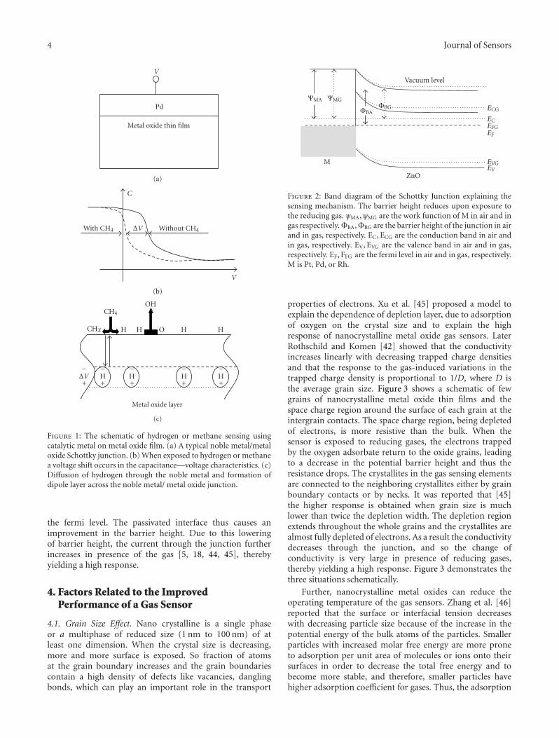
Bhattacharyya et al. [120] studied the sol-gel grown ZnO-based gas sensors in the resistive mode. Pd-Ag and Rhcontacts were found to produce a relatively lower optimumtemperature of 250◦C for sensing compared to 300◦C forPt contact. Further, Rh contact showed the higher response(83.6%) than Pd-Ag and Pt (Figure 13). It was furtherreported that the response and recovery time are shorter forPd-Ag compared to Rh and Pt contacts, most probably dueto the fact that solubility and diffusivity of hydrogen obtainedfrom methane dissociation is higher for Pd-Ag compared toboth Pt and Rh [128–131].
Basu et al. [126, 127] have studied electrochemicallygrown ZnO-based MIM Schottky gas sensors and the effectof different catalyst metals (Rh, Pt, and Pd-Ag) on methanesensing. The response versus temperature curves for differentnoble metal catalysts in pure nitrogen is shown in Figure 14and it is observed that Rh gives higher response than Pd-Ag and Pt (Rh>Pd-Ag>Pt). In fact, the catalytic effect of Rhfor dissociation of methane or hydrogen is stronger than Pdand Pt. In literature, it can be found that catalytic activityof Pd and Pt on methane or hydrogen is more or less thesame [128–131]. But Figure 14 shows a higher response withPd-Ag than Pt and thus contradicts the reported results.Figure 14(b) further shows that the response is somewhatreduced in synthetic air. It was reported that the oxygenis parallely chemisorbed on the noble metal and there is a
12 Journal of Sensors
ZnO-based MIM sensors
35030025020015010050
Temperature (◦C)
RhPd-AgPt
0
1
2
3
4
5R
espo
nse
(a)
ZnO-based MIM sensors
300250200150
Temperature (◦C)
RhPd-AgPt
0
1
2
3
4
Res
pon
se
(b)
Figure 14: Response versus temperature curves of Pt/ZnO/ZnO, Pd-Ag (26%)/ZnO/Zn, and Rh/ZnO/Zn MIM sensors in the presence of1% methane in (a) pure nitrogen and in (b) synthetic air.
competitive equilibrium between oxygen and hydrogen asthe adsorbates on ZnO. As a result it may well be depictedthat the adsorption sites for hydrogen are reduced andchemisorbed hydrogen reacts with oxygen instead of gettingdiffused into the noble metal/ZnO junction to produce H2Omolecules and thus reduce the current through the electrodes[126, 127]. Therefore, a lower response to hydrogen isobtained in synthetic air. The reactivity depends on thecatalytic properties of the metal surface and differs betweendifferent metals. Since the OH formation energy barrieris much lower on Pt than Pd-Ag, most of the hydrogenproduced by the dissociation of methane produces OHmolecule for Pt contact. Then the water formation needsmore than one step and thus the kinetics of sensing becomesslower.
Therefore, the devices using Pt as catalytic metal exhibitlower response and relatively longer response time thanPd-Ag for all the cases. The OH formation energy of Rhis higher than both Pd-Ag and Pt [128–131] and so Rhcatalytic metal contact gives higher response than Pd-Ag andPt. This corroborates the experimental results obtained byBhattacharyya et al. [120].
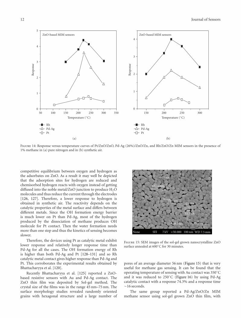
Recently Bhattacharyya et al. [125] reported a ZnO-based resistive sensors with Au and Pd-Ag contact. TheZnO thin film was deposited by Sol-gel method. Thecrystal size of the films was in the range 45 nm–75 nm. Thesurface morphology studies revealed randomly orientedgrains with hexagonal structure and a large number of
None SEI 7 kV ×50.000 100 nm WD 7.5 mm
75 nm
52.6 nm
56 nm
45.7 nm
48.2 nm
Figure 15: SEM images of the sol-gel grown nanocrystalline ZnOsurface annealed at 600◦C for 30 minutes.
pores of an average diameter 56 nm (Figure 15) that is veryuseful for methane gas sensing. It can be found that theoperating temperature of sensing with Au contact was 350◦Cand it was reduced to 250◦C (Figure 16) by using Pd-Agcatalytic contact with a response 74.3% and a response time∼16 seconds.
The same group reported a Pd-Ag/ZnO/Zn MIMmethane sensor using sol-gel grown ZnO thin film, with

Journal of Sensors 13
4003002001000
Temperature (◦C)
Pd-AgAu
0
10
20
30
40
50
60
70
80
Res
pon
se(%
)
Figure 16: Response as a function of temperature.
None SEI 5 kV ×30.000 100 nm WD 6.4 mm
Figure 17: FESEM pictures of ZnO thin films grown electrochemi-cally, with the magnification (× 30 000).
an operating temperature of 250◦C and a response time∼11 seconds.
Basu [132] reduced the operating temperature ofmethane sensing to 100◦C or less by using electrochemicallygrown nanocrystalline-nanoporous ZnO thin film and bymodifying the oxide surface with Pd. Two different deviceconfigurations, for example, a planar structure and a metal-active insulator-metal (MIM) sandwich structure, bothworking on Schottky barrier mode were designed, fabricated,and tested for methane sensing. Pd-Ag alloy was used as thecatalytic electrode (0.2 μm) contact for both the planar andMIM configurations.
Figure 17 shows the FESEM picture of the electrochem-ically grown nanocrystalline ZnO thin film. The crystallitesize obtained was below 10 nm with a uniform distributionof the nanopores (size).
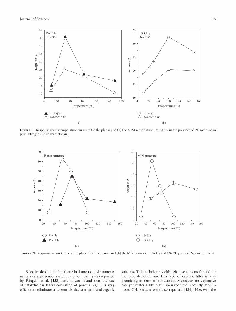
The variations of the response with operating tempera-ture and with biasing voltage using 1% methane in nitrogenand in synthetic air were studied. The maximum responsewas obtained at 70◦C and 100◦C for the planar and the MIMsensor structures, respectively, with 3 V forward bias for both(Figures 18 and 19).
The Pd-modified nanocrystalline ZnO (below 10 nm)enhances the oxygen spillover process on ZnO matrix,resulting in a large amount of chemisorbed oxygen that yieldsa high electrostatic potential across the Pd-Ag/ZnO Schottkyinterface.
The change of current in presence of methane is relativelyhigher for the planar structure that has two Schottky contactswith double barriers compared to the MIM structure withone Pd-Ag/ZnO junction. The performance was somewhatreduced in synthetic air for both the sensor structures dueto a competitive equilibrium between oxygen (from air) andhydrogen as the adsorbates on ZnO. As a result the adsorp-tion sites for hydrogen and thus the amount of hydrogendiffusing across the Pd-Ag/ZnO junction are reduced. Thetemperature for maximum response was reduced to 70◦Cfor the planar and 100◦C for the MIM structures for thePd-modified ZnO nanocrystals. The possible reason for theresponse at substantially low temperature was mentioned asdue to increased surface free energy of the nanocrystallineZnO surface. Presence of dispersed Pd nano particles overZnO surface further reduces the adsorption energy. As aresult the sensors respond at considerably low temperatureand with short time of response. It is worth mentioning herethat imperfect structural orientation of the polycrystallinesensing layer (ZnO) also modulates the gas adsorptionbehavior and thus the sensing parameters.
Figure 20 demonstrates that the sensors using Pd modi-fied ZnO thin films show temperature dependent selectivityfor methane and hydrogen in presence of each other. For theplanar sensors hydrogen response is maximum at 50◦C wherethe response for methane is very low. At 70◦C both hydrogenand methanerespond almost to the same extent. On the otherhand, MIM sensors show distinct selectivity for methane at100◦C where hydrogen response is almost zero.
Methane actually first dissociates to produce molecularhydrogen that subsequently decomposes catalytically toatomic hydrogen. The atomic hydrogen then takes part ingas sensing reaction. Therefore, the temperature for sensingmethane is always higher than that of hydrogen.
The response time and recovery time were calculatedfrom the transient response curves for different concentra-tions of methane and are shown in Table 1 .
Table 1 shows that the response and recovery times of theMIM sensor are relatively shorter than the planar sensor. Thepossible interpretation has been given that the separationbetween two electrodes for the planar configuration is larger(2 mm) than the MIM (8 μm) configuration, resulting in therapid current flow kinetics for the MIM configuration.

14 Journal of Sensors
1% CH4 (N2)
160140120100806040
Temperature (◦C)
Planar structureMIM structure
15
20
25
30
35
40
45
50
55R
espo
nse
(S)
(a)
1% CH4 (N2)
76543210
Voltage (V)
Planar structure (70◦C)MIM structure (100◦C)
5
10
15
20
25
30
35
40
45
50
55
Res
pon
se(S
)
(b)
Figure 18: (a) Response versus temperature curves at 3 V and (b) response versus voltage curves, for planar and MIM sensor structures at70◦C and 100◦C.
Table 1: The sensing results of the planar structures at 70◦C and MIM structures at 100◦C for different concentrations of methane usingnitrogen and synthetic air as carrier gases.
% CH4 Response Response time (s) Recovery time (s)
Planar MIM Planar MIM Planar MIM
Nitrogen Syntheticair
Nitrogen Syntheticair
Nitrogen Syntheticair
Nitrogen Syntheticair
Nitrogen Syntheticair
Nitrogen Syntheticair
0.01 21.2 9.2 18.2 6.5 16.2 19.2 10.2 13.2 33.2 34.2 18.7 20.3
0.05 25.4 14.6 22.3 11.4 13.3 17.4 6.7 9.3 30.3 32.8 17.2 19.2
0.1 39.3 18.3 23.2 16.8 11.1 16.4 6.03 8.2 27.5 29.6 16.8 17.3
0.5 42.2 21.6 25.2 17.2 8.4 15.2 4.02 6.9 25.7 27.4 16.1 17.1
1 47.5 25.7 32.2 20.4 4.6 12.6 2.69 4.2 22.7 23.4 16.0 16.2
The longer time of recovery was due to slower rate ofdesorption being interfered by the presence of air after themethane flow was cut off.
This investigation highlights the fact that the temperatureof sensing methane at 100◦C using Pd-Ag/Pd: ZnO/Zn MIMdevice configuration is suitable for practical applications asdue to minimum interference from humidity.
There are very few reports on metal oxide-based methanegas sensors with high response and shorter response andrecovery time. So far the reported sensor structures basedon oxide semiconductors and operating in the resis-tive mode at high temperature showed relatively longerresponse (>10 seconds) and recovery (>40 seconds) timefor methane sensing. In this investigation, particularly the
MIM sensor showed good response (∼32), shorter response(∼2.69 seconds), and recovery (∼16 seconds) times as com-pared to the values reported by others [1–7, 91–105, 118–127, 133, 134].
Figure 21 presents the stability of both types of sensorstructures. For 1% methane in nitrogen as carrier gas thestudy was continued for 33 days and showed a stableperformance. In synthetic air the stability studied for about9 hours was appreciably good.
5.3. Other Metal Oxide-Based Methane Gas Sensors. Apartfrom the ZnO-and SnO2-based gas sensors, there are fewmetal oxides that give response towards the me-thane.
Journal of Sensors 15
1% CH4
Bias: 3 V
160140120100806040
Temperature (◦C)
NitrogenSynthetic air
10
15
20
25
30
35
40
45
50
Res
pon
se(S
)
(a)
1% CH4
Bias: 3 V
160140120100806040
Temperature (◦C)
NitrogenSynthetic air
10
15
20
25
30
35
Res
pon
se(S
)
(b)
Figure 19: Response versus temperature curves of (a) the planar and (b) the MIM sensor structures at 3 V in the presence of 1% methane inpure nitrogen and in synthetic air.
Planar structure
16014012010080604020
Temperature (◦C)
1% H2
1% CH4
0
10
20
30
40
50
60
70
Res
pon
se(S
)
(a)
MIM structure
16014012010080604020
Temperature (◦C)
1% H2
1% CH4
0
10
20
30
40
50
60
Res
pon
se(S
)
(b)
Figure 20: Response versus temperature plots of (a) the planar and (b) the MIM sensors in 1% H2 and 1% CH4 in pure N2 environment.
Selective detection of methane in domestic environmentsusing a catalyst sensor system based on Ga2O3 was reportedby Flingelli et al. [133], and it was found that the useof catalytic gas filters consisting of porous Ga2O3 is veryefficient to eliminate cross sensitivities to ethanol and organic
solvents. This technique yields selective sensors for indoormethane detection and this type of catalyst filter is verypromising in term of robustness. Moreover, no expensivecatalytic material like platinum is required. Recently, MoO3-based CH4 sensors were also reported [134]. However, the

16 Journal of Sensors
Voltage 3 V1% CH4 in N2
8007006005004003002001000
Time (hr)
Planar structure (70◦C)MIM structure (100◦C)
30
35
40
45
50
55
Res
pon
se(S
)
(a)
Voltage 3 V1% CH4 in synthetic air
5004003002001000
Time (min)
Planar structure (70◦C)MIM structure (100◦C)
22
24
26
28
30
32
34
36
Res
pon
se
(b)
Figure 21: Stability study of both types of sensor structures using nitrogen as carrier gases.
sensor was operated at 500◦C and the sensitivity for methanewas quite poor.
6. Conclusion
This review article has focused on the recent achievementon the research and development of methane gas sensorsusing inexpensive metal oxides and the effect of noble metals,either as catalytic contact electrodes or as the sensitizingagents. Among them SnO2 and ZnO sensors have beenwidely studied and have shown most promising results ongas response in terms of sensing temperature and voltage,sensitivity, time of response and stability. NanocrystallineZnO, after sensitization with Pd nanoparticles has shown thelowest temperature of methane sensing so far reported. Gassensing mechanism has been briefly discussed from the pointof view adsorption-desorption activation and the influenceof noble metals.
Acknowledgments
The authors thankfully acknowledge the help and coop-eration of Prof. H. Saha, Coordinator, and IC Design &Fabrication Centre, Department of Electronics & Telecom-munication Engineering. Jadavpur University, Kolkata, forkindly providing the laboratory facilities. Thanks are alsodue to Dr. P. Bhattacharya, Ms. N. Saha, and Mr. S. K.Jana of the gas sensor group. P. K. Basu acknowledges CSIR,Government. of India, for kindly providing a Senior ResearchFellowship (SRF).
References
[1] M. Fleischer and H. Meixner, “A selective CH4 sensor usingsemiconducting Ga2O3 thin films based on temperatureswitching of multigas reactions,” Sensors and Actuators B, vol.25, no. 1–3, pp. 544–547, 1995.
[2] J. Wollenstein, M. Burgmair, G. Plescher, et al., “Cobalt oxidebased gas sensors on silicon substrate for operation at lowtemperatures,” Sensors and Actuators B, vol. 93, no. 1–3, pp.442–448, 2003.
[3] J. B. W. H. Brattain, “Surface properties of germanium,” BellSystem Technical Journal, vol. 32, 1952.
[4] D. M. Wilson, S. Hoyt, J. Janata, K. Booksh, and L. Obando,“Chemical sensors for portable, handheld field instruments,”IEEE Sensors Journal, vol. 1, no. 4, pp. 256–274, 2001.
[5] J. Xu, Q. Pan, Y. Shun, and Z. Tian, “Grain size controland gas sensing properties of ZnO gas sensor,” Sensors andActuators B, vol. 66, no. 1, pp. 277–279, 2000.
[6] A. Trinchi, S. Kaciulis, L. Pandolfi, et al., “Characterizationof Ga2O3 based MRISiC hydrogen gas sensors,” Sensors andActuators B, vol. 103, no. 1-2, pp. 129–135, 2004.
[7] X. Chen, W. Lu, W. Zhu, S. Y. Lim, and S. A. Akbar,“Structural and thermal analyses on phase evolution of sol-gel (Ba,Sr)TiO3 thin films,” Surface and Coatings Technology,vol. 167, no. 2-3, pp. 203–206, 2003.
[8] E. Comini, M. Ferroni, V. Guidi, G. Faglia, G. Martinelli, andG. Sberveglieri, “Nanostructured mixed oxides compoundsfor gas sensing applications,” Sensors and Actuators B, vol. 84,no. 1, pp. 26–32, 2002.
[9] M. Rumyantseva, V. Kovalenko, A. Gaskov, et al., “Nanocom-posites SnO2/Fe2O3: sensor and catalytic properties,” Sensorsand Actuators B, vol. 118, no. 1-2, pp. 208–214, 2006.

Journal of Sensors 17
[10] T. Islam and H. Saha, “Hysteresis compensation of a poroussilicon relative humidity sensor using ANN technique,”Sensors and Actuators B, vol. 114, no. 1, pp. 334–343, 2006.
[11] G. Kenanakis, D. Vernardou, E. Koudoumas, G. Kiriakidis,and N. Katsarakis, “Ozone sensing properties of ZnO nanos-tructures grown by the aqueous chemical growth technique,”Sensors and Actuators B, vol. 124, no. 1, pp. 187–191, 2007.
[12] A. Teleki, S. E. Pratsinis, K. Kalyanasundaram, and P. I.Gouma, “Sensing of organic vapors by flame-made TiO2
nanoparticles,” Sensors and Actuators B, vol. 119, no. 2, pp.683–690, 2006.
[13] J. Wollenstein, M. Burgmair, G. Plescher, et al., “Cobalt oxidebased gas sensors on silicon substrate for operation at lowtemperatures,” Sensors and Actuators B, vol. 93, no. 1–3, pp.442–448, 2003.
[14] A. Trinch, W. Wlodarski, Y. X. Li, G. Feglia, and G.Sberveglieri, “Pt,Ga2O3/SiC MRSiC devices: a study of thehydrogen response,” Journal of Physics D, vol. 38, p. 754, 2005.
[15] L. Talazac, F. Barbarin, C. Varenne, L. Mazet, S. Pellier, and C.Soulier, “Gas sensing properties of pseudo-Schottky diodeson p-type indium phosphide substrates—application to O3
and NO2 monitoring in urban ambient air,” Sensors andActuators B, vol. 83, no. 1–3, pp. 149–159, 2002.
[16] K.-W. Lin, H.-I. Chen, C.-T. Lu, et al., “A hydrogen sensingPd/InGaP metal-semiconductor (MS) Schottky diode hydro-gen sensor,” Semiconductor Science and Technology, vol. 18,no. 7, pp. 615–619, 2003.
[17] P. K. Basu, S. K. Jana, M. K. Mitra, H. Saha, and S. Basu,“Hydrogen gas sensors using anodically prepared and surfacemodified nanoporous ZnO thin films,” Sensor Letters, vol. 6,no. 5, pp. 699–704, 2008.
[18] P. K. Basu, P. Bhattacharyya, N. Saha, H. Saha, and S.Basu, “Methane sensing properties of platinum catalysednano porous zinc oxide thin films derived by electrochemicalanodization,” Sensor Letters, vol. 6, no. 1, pp. 219–225, 2008.
[19] M. Stamataki, D. Tsamakis, N. Brilis, I. Fasaki, A. Gian-noudakos, and M. Kompitsas, “Hydrogen gas sensors basedon PLD grown NiO thin film structures,” Physica StatusSolidi, vol. 205, no. 8, pp. 2064–2068, 2008.
[20] S. Basu and S. K. Hazra, “ZnO p-n homojunctions forhydrogen gas sensors at elevated temperature,” Asian Journalof Physics, vol. 14, p. 65, 2005.
[21] S. K. Hazra and S. Basu, “Hydrogen sensitivity of ZnO p-nhomojunctions,” Sensors and Actuators B, vol. 117, no. 1, pp.177–182, 2006.
[22] K.-K. Baek and H. L. Tuller, “Electronic characterization ofZnO/CuO heterojunctions,” Sensors and Actuators B, vol. 13,no. 1–3, pp. 238–240, 1993.
[23] Y. Ushio, M. Miyayama, and H. Yanagida, “Effects of interfacestates on gas-sensing properties of a CuO/ZnO thin-filmheterojunction,” Sensors and Actuators B, vol. 17, no. 3, pp.221–226, 1994.
[24] Y. Hu, X. Zhou, Q. Han, Q. Cao, and Y. Huang, “Sensingproperties of CuO-ZnO heterojunction gas sensors,” Mate-rials Science and Engineering B, vol. 99, no. 1–3, pp. 41–43,2003.
[25] Z. Ling, C. Leach, and R. Freer, “Heterojunction gas sensorsfor environmental NO2 and CO2 monitoring,” Journal of theEuropean Ceramic Society, vol. 21, no. 10-11, pp. 1977–1980,2001.
[26] W.-Y. Chung, D.-D. Lee, and B.-K. Sohn, “Effects of addedTiO2 on the characteristics of SnO2-based thick film gassensors,” Thin Solid Films, vol. 221, no. 1-2, pp. 304–310,1992.
[27] K. Zakrzewska, M. Radecka, and M. Rekas, “Effect of Nb, Cr,Sn additions on gas sensing properties of TiO2 thin films,”Thin Solid Films, vol. 310, no. 1-2, pp. 161–166, 1997.
[28] M. Radecka, K. Zakrzewska, and M. Rekas, “SnO2-TiO2 solidsolutions for gas sensors,” Sensors and Actuators B, vol. 47, no.1–3, pp. 194–204, 1998.
[29] V. Dusastre and D. E. Williams, “Gas-sensitive resistor prop-erties of the solid solution series Tix(Sn1−ySby)1−xO2(0 < x <1, y = 0, 0.01, 0.05),” Journal of Materials Chemistry, vol. 9,no. 2, pp. 445–450, 1999.
[30] K. Zakrzewska, “Mixed oxides as gas sensors,” Thin SolidFilms, vol. 391, no. 2, pp. 229–238, 2001.
[31] J. L. Solis and V. Lantto, “A study of gas-sensing properties ofsputtered α-SnWO4 thin films,” Sensors and Actuators B, vol.25, no. 1–3, pp. 591–595, 1995.
[32] J. L. Solis and V. Lantto, “Gas-sensing properties of differentα-SnWO4-based thick films,” Physica Scripta T, vol. 69, pp.281–285, 1997.
[33] P. Nelli, L. E. Depero, M. Ferroni, et al., “Sub-ppm NO2
sensors based on nanosized thin films of titanium-tungstenoxides,” Sensors and Actuators B, vol. 31, no. 1-2, pp. 89–92,1996.
[34] L. E. Depero, M. Ferroni, V. Guidi, et al., “Preparation andmicro-structural characterization of nanosized thin film ofTiO2-WO3 as a novel material with high sensitivity towardsNO2,” Sensors and Actuators B, vol. 36, no. 1–3, pp. 381–383,1996.
[35] V. Guidi, M. C. Carotta, M. Ferroni, et al., “Preparation ofnanosized titania thick and thin films as gas-sensors,” Sensorsand Actuators B, vol. 57, no. 1–3, pp. 197–200, 1999.
[36] E. Comini, M. Ferroni, V. Guidi, G. Faglia, G. Martinelli, andG. Sberveglieri, “Nanostructured mixed oxides compoundsfor gas sensing applications,” Sensors and Actuators B, vol. 84,no. 1, pp. 26–32, 2002.
[37] P. Bhattacharyya, P. K. Basu, C. Lang, H. Saha, and S. Basu,“Noble metal catalytic contacts to sol-gel nanocrystalline zincoxide thin films for sensing methane,” Sensors and ActuatorsB, vol. 129, no. 2, pp. 551–557, 2008.
[38] H.-W. Cheong and M.-J. Lee, “Sensing characteristics andsurface reaction mechanism of alcohol sensors based ondoped SnO2,” Journal of Ceramic Processing Research, vol. 7,no. 3, pp. 183–191, 2006.
[39] L. Castaneda, “Effects of palladium coatings on oxygensensors of titanium dioxide thin films,” Materials Science andEngineering B, vol. 139, no. 2-3, pp. 149–154, 2007.
[40] V. R. Shinde, T. P. Gujar, and C. D. Lokhande, “Enhancedresponse of porous ZnO nanobeads towards LPG: effect ofPd sensitization,” Sensors and Actuators B, vol. 123, no. 2, pp.701–706, 2007.
[41] S. W. Hla, P. Lacovig, G. Comelli, A. Baraldi, M. Kiskinova,and R. Rosei, “Orientational anisotropy in oxygen dissocia-tion on Rh(110),” Physical Review B, vol. 60, no. 11, pp. 7800–7803, 1999.
[42] A. Rothschild and Y. Komem, “The effect of grain size onthe sensitivity of nanocrystalline metal-oxide gas sensors,”Journal of Applied Physics, vol. 95, no. 11, pp. 6374–6380,2004.
[43] S. L. Tait, Z. Dohnalek, C. T. Campbell, and B. D. Kay,“Methane adsorption and dissociation and oxygen adsorp-tion and reaction with CO on Pd nanoparticles on MgO(1 00) and on Pd(1 1 1),” Surface Science, vol. 591, no. 1–3, pp.90–107, 2005.

18 Journal of Sensors
[44] M. Ali, V. Cimalla, V. Lebedev, et al., “Pt/GaN Schottkydiodes for hydrogen gas sensors,” Sensors and Actuators B, vol.113, no. 2, pp. 797–804, 2006.
[45] C. Xu, J. Tamaki, N. Miura, and N. Yamazoe, “Relationshipbetween gas sensitivity and microstructure of porous SnO2,”Journal of The Electrochemical Society, vol. 58, p. 1143, 1990.
[46] H. Zhang, R. L. Penn, R. J. Hamers, and J. F. Banfield,“Enhanced adsorption of molecules on surfaces of nanocrys-talline particles,” Journal of Physical Chemistry B, vol. 103, no.22, pp. 4656–4662, 1999.
[47] C. Xu, J. Tamaki, N. Miura, and N. Yamazoe, “Grain sizeeffects on gas sensitivity of porous SnO2-based elements,”Sensors and Actuators B, vol. 3, no. 2, pp. 147–155, 1991.
[48] M. Tiemann, “Porous metal oxides as gas sensors,” Chem-istry, vol. 13, no. 30, pp. 8376–8388, 2007.
[49] G. Sakai, N. S. Baik, N. Miura, and N. Yamazoe, “Gassensing properties of tin oxide thin films fabricated fromhydrothermally treated nanoparticles: dependence of CO andH2 response on film thickness,” Sensors and Actuators B, vol.77, no. 1-2, pp. 116–121, 2001.
[50] P. K. Basu, P. Bhattacharyya, N. Saha, H. Saha, and S. Basu,“The superior performance of the electrochemically grownZnO thin films as methane sensor,” Sensors and Actuators B,vol. 133, no. 2, pp. 357–363, 2008.
[51] G. Korotcenkov, V. Brinzari, J. Schwank, M. DiBattista,and A. Vasiliev, “Peculiarities of SnO2 thin film depositionby spray pyrolysis for gas sensor application,” Sensors andActuators B, vol. 77, no. 1-2, pp. 244–252, 2001.
[52] G. Sakai, N. Matsunaga, K. Shimanoe, and N. Yamazoe,“Theory of gas-diffusion controlled sensitivity for thin filmsemiconductor gas sensor,” Sensors and Actuators B, vol. 80,no. 2, pp. 125–131, 2001.
[53] F. Hossein-Babaei and M. Orvatinia, “Analysis of thicknessdependence of the sensitivity in thin film resistive gassensors,” Sensors and Actuators B, vol. 89, no. 3, pp. 256–261,2003.
[54] D. Ding, Z. Chen, and C. Lu, “Hydrogen sensing ofnanoporous palladium films supported by anodic aluminumoxides,” Sensors and Actuators B, vol. 120, no. 1, pp. 182–186,2006.
[55] I. Lundstrom, H. Sundgren, F. Winquist, M. Eriksson, C.Krantz-Rulcker, and A. Lloyd-Spetz, “Twenty-five years offield effect gas sensor research in Linkoping,” Sensors andActuators B, vol. 121, no. 1, pp. 247–262, 2007.
[56] M. Lofdahl, C. Utaiwasin, A. Carlsson, I. Lundstrom, andM. Eriksson, “Gas response dependence on gate metalmorphology of field-effect devices,” Sensors and Actuators B,vol. 80, no. 3, pp. 183–192, 2001.
[57] M. Armgarth and C. Nylander, “Blister formation in Pd gateMIS hydrogen sensors,” IEEE Electron Device Letters, vol. 3,no. 12, pp. 384–386, 1982.
[58] S. C. Su, J. N. Carstens, and A. T. Bell, “A study of thedynamics of Pd oxidation and PdO reduction by H2 andCH4,” Journal of Catalysis, vol. 176, no. 1, pp. 125–135, 1998.
[59] M. Wang and Y. Feng, “Palladium-silver thin film forhydrogen sensing,” Sensors and Actuators B, vol. 123, no. 1,pp. 101–106, 2007.
[60] R. C. Hughes, W. K. Schubert, T. E. Zipperian, J. L.Rodriguez, and T. A. Plut, “Thin film palladium and shiveralloys and layers for metal-insulator-semiconductor sensors,”Journal of Applied Physics, vol. 62, p. 1074, 1987.
[61] V. A. Drozdov, P. G. Tsyrulnikov, V. V. Popovskii, N. N.Bulgakov, E. M. Moroz, and T. G. Galeev, “Comparative studyof the activity of Al-Pd and Al-Pt catalysts in deep oxidationof hydrocarbons,” Reaction Kinetics and Catalysis Letters, vol.27, no. 2, pp. 425–427, 1985.
[62] B. L. Zhu, C. S. Xie, D. W. Zeng, W. L. Song, and A. M.Wang, “Investigation of gas sensitivity of Sb-doped ZnOnanoparticles,” Materials Chemistry and Physics, vol. 89, no.1, pp. 148–153, 2005.
[63] M. N. Rumyantseva, V. V. Kovalenko, A. M. Gas’kov, and T.Pagnier, “Metal-oxide based nanocomposites as materials forgas sensors,” Russian Journal of General Chemistry, vol. 78, no.5, pp. 1081–1092, 2008.
[64] F. Volkenshtein, Electronic Theory of Catalysis on Semiconduc-tors, Fizmatgiz, Moscow, Russia, 1960.
[65] G. Korotcenkov, “Gas response control through structuraland chemical modification of metal oxide films: state of theart and approaches,” Sensors and Actuators B, vol. 107, no. 1,pp. 209–232, 2005.
[66] J. F. McAleer, P. T. Moseley, J. O. W. Norris, D. E. Williams,and B. C. Tofield, “Tin dioxide gas sensors—part 2: the roleof surface additives,” Journal of the Chemical Society, FaradayTransactions 1, vol. 84, no. 2, pp. 441–457, 1988.
[67] V. Brinzari, G. Korotcenkov, J. Schwank, and Y. Boris,“Chemisorptionoal approach to kinetic analysis of SnO2:Pd-based thin film gas sensors (TFGS),” Journal of Optoelectron-ics and Advanced Materials, vol. 4, no. 1, p. 147, 2002.
[68] G. Korotcenkov, V. Brinzari, Y. Boris, M. Ivanov, J. Schwank,and J. Morante, “Influence of surface Pd doping on gassensing characteristics of SnO2 thin films deposited by spraypirolysis,” Thin Solid Films, vol. 436, no. 1, pp. 119–126, 2003.
[69] V. R. Shinde, T. P. Gujar, and C. D. Lokhande, “Enhancedresponse of porous ZnO nanobeads towards LPG: effect ofPd sensitization,” Sensors and Actuators B, vol. 123, no. 2, pp.701–706, 2007.
[70] W. Gopel and K. D. Schierbaum, “SnO2 sensors: currentstatus and future prospects,” Sensors and Actuators B, vol. 26,no. 1–3, pp. 1–12, 1995.
[71] M. J. Madou and S. R. Morrison, Chemical Sensing with Solid-State Devices, Academic Press, New York, NY, USA, 1989.
[72] J.-H. Sung, Y.-S. Lee, J.-W. Lim, Y.-H. Hong, and D.-D. Lee,“Sensing characteristics of tin dioxide/gold sensor preparedby coprecipitation method,” Sensors and Actuators B, vol. 66,no. 1, pp. 149–152, 2000.
[73] K. L. Chopra, S. Major, and D. K. Pandya, “Transparentconductors—a status review,” Thin Solid Films, vol. 102, no.1, pp. 1–46, 1983.
[74] T. W. Kim, D. U. Lee, J. H. Lee, D. C. Choo, M. Jung, and Y. S.Yoon, “Structural, electrical, and optical properties of SnO2
nanocrystalline thin films grown on p-InSb (111) substrates,”Journal of Applied Physics, vol. 90, no. 1, pp. 175–180, 2001.
[75] G. G. Mandayo, E. Castano, F. J. Gracia, A. Cirera, A.Cornet, and J. R. Morante, “Strategies to enhance the carbonmonoxide sensitivity of tin oxide thin films,” Sensors andActuators B, vol. 95, no. 1–3, pp. 90–96, 2003.
[76] H. Ogawa, M. Nishikawa, and A. Abe, “Hall measurementstudies and an electrical conduction model of tin oxideultrafine particle films,” Journal of Applied Physics, vol. 53, no.6, pp. 4448–4455, 1982.
[77] V. R. Katti, A. K. Debnath, K. P. Muthe, et al., “Mechanism ofdrifts in H2S sensing properties of SnO2:CuO composite thin

Journal of Sensors 19
film sensors prepared by thermal evaporation,” Sensors andActuators B, vol. 96, no. 1-2, pp. 245–252, 2003.
[78] B.-K. Min and S.-D. Choi, “SnO2 thin film gas sensorfabricated by ion beam deposition,” Sensors and Actuators B,vol. 98, no. 2-3, pp. 239–246, 2004.
[79] G. Korotcenkov, V. Brinzari, V. Golovanov, and Y. Blinov,“Kinetics of gas response to reducing gases of SnO2 films,deposited by spray pyrolysis,” Sensors and Actuators B, vol.98, no. 1, pp. 41–45, 2004.
[80] S. Shukla, S. Patil, S. C. Kuiry, et al., “Synthesis andcharacterization of sol-gel derived nanocrystalline tin oxidethin film as hydrogen sensor,” Sensors and Actuators B, vol.96, no. 1-2, pp. 343–353, 2003.
[81] G. Sberveglieri, “Classical and novel techniques for thepreparation of SnO2 thin-film gas sensors,” Sensors andActuators B, vol. 6, no. 1–3, pp. 239–247, 1992.
[82] R. Dolbec, M. A. El Khakani, A. M. Serventi, and R. G. Saint-Jacques, “Influence of the nanostructural characteristics onthe gas sensing properties of pulsed laser deposited tin oxidethin films,” Sensors and Actuators B, vol. 93, no. 1–3, pp. 566–571, 2003.
[83] D. B. Chrisey and G. K. Hubler, Eds., Pulsed Laser Depositionof Thin Films, John Wiley & Sons, New York, NY, USA, 1994.
[84] M. C. Carotta, V. Guidi, G. Martinelli, M. Nagliati, D.Puzzovio, and D. Vecchi, “Sensing of volatile alkanes bymetal-oxide semiconductors,” Sensors and Actuators B, vol.130, no. 1, pp. 497–501, 2008.
[85] H. H. Kung, “Oxidative dehydrogenation of light (C2 to C4)alkanes,” Advanced Catalyst, vol. 40, p. 1, 1994.
[86] I.-C. Marcu, J.-M. M. Millet, and J.-M. Herrmann, “Semi-conductive and redox properties of Ti and Zr pyrophosphatecatalysts (TiP2O7 and ZrP2O7). Consequences for the oxida-tive dehydrogenation of n-butane,” Catalysis Letters, vol. 78,no. 1–4, pp. 273–279, 2002.
[87] I.-C. Marcu, J.-M. M. Millet, and I. Sandulescu, “Oxidativedehydrogenation of isobutane over a titanium pyrophos-phate catalyst,” Journal of the Serbian Chemical Society, vol.70, no. 6, pp. 791–798, 2005.
[88] M. C. Carotta, A. Cervi, A. Giberti, et al., “Ethanol interfer-ence in light alkane sensing by metal-oxide solid solutions,”Sensors and Actuators B, vol. 136, no. 2, pp. 405–409, 2009.
[89] M. C. Carotta, A. Cervi, A. Giberti, et al., “Metal-oxide solidsolutions for light alkane sensing,” Sensors and Actuators B,vol. 133, no. 2, pp. 516–520, 2008.
[90] M. C. Carotta, V. Guidi, G. Martinelli, M. Nagliati, D.Puzzovio, and D. Vecchi, “Sensing of volatile alkanes bymetal-oxide semiconductors,” Sensors and Actuators B, vol.130, no. 1, pp. 497–501, 2008.
[91] M. V. Vaishampayan, R. G. Deshmukh, and I. S. Mulla,“Influence of Pd doping on morphology and LPG responseof SnO2,” Sensors and Actuators B, vol. 131, no. 2, pp. 665–672, 2008.
[92] A. Cabot, A. Vila, and J. R. Morante, “Analysis of the catalyticactivity and electrical characteristics of different modifiedSnO2 layers for gas sensors,” Sensors and Actuators B, vol. 84,no. 1, pp. 12–20, 2002.
[93] N. Das, A. K. Halder, J. M. A. Sen, and H. S. Maiti,“Sonochemically prepared tin-dioxide based composition formethane sensor,” Materials Letters, vol. 60, no. 8, pp. 991–994, 2006.
[94] B.-K. Min and S.-D. Choi, “Undoped and 0.1 wt.% Ca-dopedPt-catalyzed SnO2 sensors for CH4 detection,” Sensors andActuators B, vol. 108, no. 1-2, pp. 119–124, 2005.
[95] S. Bose, S. Chakraborty, B. K. Ghosh, D. Das, A. Sen, and H.S. Maiti, “Methane sensitivity of Fe-doped SnO2 thick films,”Sensors and Actuators B, vol. 105, no. 2, pp. 346–350, 2005.
[96] F. Quaranta, R. Rella, P. Siciliano, et al., “Novel gas sensorbased on SnO2/Os thin film for the detection of methane atlow temperature,” Sensors and Actuators B, vol. 58, no. 1–3,pp. 350–355, 1999.
[97] K. Chatterjee, S. Chatterjee, A. Banerjee, et al., “The effect ofpalladium incorporation on methane sensitivity of antimonydoped tin dioxide,” Materials Chemistry and Physics, vol. 81,no. 1, pp. 33–38, 2003.
[98] J. C. Kim, H. K. Jun, J.-S. Huh, and D. D. Lee, “Tin oxide-based methane gas sensor promoted by alumina-supportedPd catalyst,” Sensors and Actuators B, vol. 45, no. 3, pp. 271–277, 1997.
[99] L. Urfels, P. Gelin, M. Primet, and E. Tena, “Completeoxidation of methane at low temperature over Pt catalystssupported on high surface area SnO2,” Topics in Catalysis, vol.30-31, pp. 427–432, 2004.
[100] C. K. Kim, J. H. Lee, S. M. Choi, et al., “Pd- and Pt-SiC Schottky diodes for detection of H2 and CH4 at hightemperature,” Sensors and Actuators B, vol. 77, no. 1-2, pp.455–462, 2001.
[101] S. Chakraborty, A. Sen, and H. S. Maiti, “Complex planeimpedance plot as a figure of merit for tin dioxide-basedmethane sensors,” Sensors and Actuators B, vol. 119, no. 2,pp. 431–434, 2006.
[102] K. R. Han, C.-S. Kim, K. T. Kang, H. J. Koo, D. Kang II,and J. He, “Development of SnO2 based semiconductor gassensor with Fe2O3 for detection of combustible gas,” Journalof Electroceramics, vol. 10, no. 1, pp. 69–73, 2003.
[103] V. V. Malyshev and A. V. Pislyakov, “Dynamic propertiesand sensitivity of semiconductor metal-oxide thick-filmsensors to various gases in air gaseous medium,” Sensors andActuators B, vol. 96, no. 1-2, pp. 413–434, 2003.
[104] M. Saha, A. Banerjee, A. K. Halder, J. Mondal, A. Sen, and H.S. Maiti, “Effect of alumina addition on methane sensitivityof tin dioxide thick films,” Sensors and Actuators B, vol. 79,no. 2-3, pp. 192–195, 2001.
[105] A. Chen, S. Bai, B. Shi, Z. Liu, D. Li, and C. C. Liu, “Methanegas-sensing and catalytic oxidation activity of SnO2-In2O3
nanocomposites incorporating TiO2,” Sensors and ActuatorsB, vol. 135, no. 1, pp. 7–12, 2008.
[106] X. L. Cheng, H. Zhao, L. H. Huo, S. Gao, and J. G. Zhao,“ZnO nanoparticulate thin film: preparation, characteriza-tion and gas-sensing property,” Sensors and Actuators B, vol.102, no. 2, pp. 248–252, 2004.
[107] M. Suchea, S. Christoulakis, K. Moschovis, N. Katsarakis,and G. Kiriakidis, “ZnO transparent thin films for gas sensorapplications,” Thin Solid Films, vol. 515, no. 2, pp. 551–554,2006.
[108] G. Eranna, B. C. Joshi, D. P. Runthala, and R. P. Gupta,“Oxide materials for development of integrated gas sensors–a comprehensive review,” Critical Reviews in Solid State andMaterials Sciences, vol. 29, no. 3-4, pp. 111–188, 2004.
[109] S. Cho, J. Ma, Y. Kim, Y. Sun, G. K. L. Wong, and J.B. Ketterson, “Photoluminescence and ultraviolet lasing ofpolycrystalline ZnO thin films prepared by the oxidation ofthe metallic Zn,” Applied Physics Letters, vol. 75, no. 18, pp.2761–2763, 1999.
[110] R. Bel Hadj Tahar, “Structural and electrical propertiesof aluminum-doped zinc oxide films prepared by sol-gelprocess,” Journal of the European Ceramic Society, vol. 25, no.14, pp. 3301–3306, 2005.

20 Journal of Sensors
[111] A. Ashida, T. Nagata, and N. Fujimura, “Electro-optical effectin ZnO:Mn thin films prepared by Xe sputtering,” Journal ofApplied Physics, vol. 99, no. 1, Article ID 013509, 4 pages,2006.
[112] S. Muthukumar, C. R. Gorla, N. W. Emanetoglu, S. Liang,and Y. Lu, “Control of morphology and orientation of ZnOthin films grown on SiO2/Si substrates,” Journal of CrystalGrowth, vol. 225, no. 2–4, pp. 197–201, 2001.
[113] J. F. Muth, R. M. Kolbas, A. K. Sharma, S. Oktyabrsky, andJ. Narayan, “Excitonic structure and absorption coefficientmeasurements of ZnO single crystal epitaxial films depositedby pulsed laser deposition,” Journal of Applied Physics, vol. 85,no. 11, pp. 7884–7887, 1999.
[114] M. Jin, J. Feng, Z. De-Heng, M. Hong-Lei, and L. Shu-Ying,“Optical and electronic properties of transparent conductingZnO and ZnO:Al films prepared by evaporating method,”Thin Solid Films, vol. 357, no. 2, pp. 98–101, 1999.
[115] H. Yan, Y. Yang, Z. Fu, et al., “Fabrication of 2D and3D ordered porous ZnO films using 3D opal templates byelectrodeposition,” Electrochemistry Communications, vol. 7,no. 11, pp. 1117–1121, 2005.
[116] G. S. Wu, T. Xie, X. Y. Yuan, et al., “Controlled synthesis ofZnO nanowires or nanotubes via sol-gel template process,”Solid State Communications, vol. 134, no. 7, pp. 485–489,2005.
[117] P. Mitra and A. K. Mukhopadhyay, “ZnO thin film asmethane sensor,” Bulletin of the Polish Academy of Sciences:Technical Sciences, vol. 55, no. 3, pp. 281–285, 2007.
[118] P. Bhattacharyya, P. K. Basu, H. Saha, and S. Basu, “Fastresponse methane sensor based on Pd(Ag)/ZnO/Zn MIMstructure,” Sensor Letters, vol. 4, no. 4, pp. 371–376, 2006.
[119] P. Bhattacharyya, P. K. Basu, H. Saha, and S. Basu, “Fastresponse methane sensor using nanocrystalline zinc oxidethin films derived by sol-gel method,” Sensors and ActuatorsB, vol. 124, no. 1, pp. 62–67, 2007.
[120] P. Bhattacharyya, P. K. Basu, C. Lang, H. Saha, and S. Basu,“Noble metal catalytic contacts to sol-gel nanocrystalline zincoxide thin films for sensing methane,” Sensors and ActuatorsB, vol. 129, no. 2, pp. 551–557, 2008.
[121] S. J. Fonash, J.-A. Roger, and C. H. S. Dupuy, “Ac equivalentcircuits for MIM structures,” Journal of Applied Physics, vol.45, no. 7, pp. 2907–2910, 1974.
[122] S. Basu and A. Dutta, “Room-temperature hydrogen sensorsbased on ZnO,” Materials Chemistry and Physics, vol. 47, no.1, pp. 93–96, 1997.
[123] M. Fleischer and H. Meixner, “A selective CH4 sensor usingsemiconducting Ga2O3 thin films based on temperatureswitching of multigas reactions,” Sensors and Actuators B, vol.25, no. 1–3, pp. 544–547, 1995.
[124] J. Wollllenstein, M. Burgmair, G. Plescher, et al., “Cobaltoxide based gas sensors on silicon substrate for operation atlow temperatures,” Sensors and Actuators B, vol. 93, no. 1–3,pp. 442–448, 2003.
[125] P. Bhattacharyya, P. K. Basu, H. Saha, and S. Basu, “Fastresponse methane sensor using nanocrystalline zinc oxidethin films derived by sol-gel method,” Sensors and ActuatorsB, vol. 124, no. 1, pp. 62–67, 2007.
[126] P. K. Basu, P. Bhattacharyya, N. Saha, H. Saha, and S. Basu,“The superior performance of the electrochemically grownZnO thin films as methane sensor,” Sensors and Actuators B,vol. 133, no. 2, pp. 357–363, 2008.
[127] P. K. Basu, P. Bhattacharyya, N. Saha, H. Saha, and S.Basu, “Methane sensing properties of platinum catalysednano porous zinc oxide thin films derived by electrochemicalanodization,” Sensor Letters, vol. 6, no. 1, pp. 219–225, 2008.
[128] R. Lober and D. Hennig, “Interaction of hydrogen withtransition metal fcc(111) surfaces,” Physical Review B, vol. 55,no. 7, pp. 4761–4765, 1997.
[129] E. P. J. Mallens, J. H. B. J. Hoebink, and G. B. Marin, “Thereaction mechanism of the partial oxidation of methane tosynthesis gas: a transient kinetic study over rhodium and acomparison with platinum,” Journal of Catalysis, vol. 167, no.1, pp. 43–56, 1997.
[130] L. Opara, B. Klein, and H. Zuchner, “Hydrogen-diffusion inPd1−xAgx(0 ≤ x ≤ 1),” Journal of Alloys and Compounds, vol.253-254, pp. 378–380, 1997.
[131] S. Eriksson, M. Nilsson, M. Boutonnet, and S. Jaras, “Partialoxidation of methane over rhodium catalysts for powergeneration applications,” Catalysis Today, vol. 100, no. 3-4,pp. 447–451, 2005.
[132] P. K. Basu, S. K. Jana, H. Saha, and S. Basu, “Low temperaturemethane sensing by electrochemically grown and surfacemodified ZnO thin films,” Sensors and Actuators B, vol. 135,no. 1, pp. 81–88, 2008.
[133] G. K. Flingelli, M. M. Fleischer, and H. Meixner, “Selectivedetection of methane in domestic environments using acatalyst sensor system based on Ga2O3,” Sensors and ActuatorsB, vol. 48, no. 1–3, pp. 258–262, 1998.
[134] S. Barazzouk, R. P. Tandon, and S. Hotchandani, “MoO3-based sensor for NO, NO2 and CH4 detection,” Sensors andActuators B, vol. 119, no. 2, pp. 691–694, 2006.

International Journal of
AerospaceEngineeringHindawi Publishing Corporationhttp://www.hindawi.com Volume 2010
RoboticsJournal of
Hindawi Publishing Corporationhttp://www.hindawi.com Volume 2014
Hindawi Publishing Corporationhttp://www.hindawi.com Volume 2014
Active and Passive Electronic Components
Control Scienceand Engineering
Journal of
Hindawi Publishing Corporationhttp://www.hindawi.com Volume 2014
International Journal of
RotatingMachinery
Hindawi Publishing Corporationhttp://www.hindawi.com Volume 2014
Hindawi Publishing Corporation http://www.hindawi.com
Journal ofEngineeringVolume 2014
Submit your manuscripts athttp://www.hindawi.com
VLSI Design
Hindawi Publishing Corporationhttp://www.hindawi.com Volume 2014
Hindawi Publishing Corporationhttp://www.hindawi.com Volume 2014
Shock and Vibration
Hindawi Publishing Corporationhttp://www.hindawi.com Volume 2014
Civil EngineeringAdvances in
Acoustics and VibrationAdvances in
Hindawi Publishing Corporationhttp://www.hindawi.com Volume 2014
Hindawi Publishing Corporationhttp://www.hindawi.com Volume 2014
Electrical and Computer Engineering
Journal of
Advances inOptoElectronics
Hindawi Publishing Corporation http://www.hindawi.com
Volume 2014
The Scientific World JournalHindawi Publishing Corporation http://www.hindawi.com Volume 2014
SensorsJournal of
Hindawi Publishing Corporationhttp://www.hindawi.com Volume 2014
Modelling & Simulation in EngineeringHindawi Publishing Corporation http://www.hindawi.com Volume 2014
Hindawi Publishing Corporationhttp://www.hindawi.com Volume 2014
Chemical EngineeringInternational Journal of Antennas and
Propagation
International Journal of
Hindawi Publishing Corporationhttp://www.hindawi.com Volume 2014
Hindawi Publishing Corporationhttp://www.hindawi.com Volume 2014
Navigation and Observation
International Journal of
Hindawi Publishing Corporationhttp://www.hindawi.com Volume 2014
DistributedSensor Networks
International Journal of


![Oxidative coupling of methane in a mixed-conducting ...Several perovskite-type oxides were already investigated as catalysts for the methane coupling reaction [ 10-15 ]. Some LaCoO3-based](https://img.pdfslide.net/doc/110x75/60ff1af5b62b793f9d3f14d4/oxidative-coupling-of-methane-in-a-mixed-conducting-several-perovskite-type.jpg)