Embed Size (px)
Citation preview
www.AlteraBoards.com
Integrated PlatformsTechnology Partners
Custom Solutions
Board Platforms
Development Tools
FPGA PLATFORMS
Your Solution... Built on BittWare
S5-PCIe-DS
• Two high-density Altera Stratix V GX/GS FPGAs
• PCIe x16 interface supporting Gen1, Gen2, or Gen3
• Four QSFP+ cages for 4 40GigE, 16 10GigE, or 4 QDR/FDR InfiniBand direct to the FPGAs
• Memory options: • upto64GBytesofDDR3SDRAMwithECC• upto4GBytesRLDRAM3• upto144MBytesQDRII+
• Eight SATA connectors, up to 6 Gbps each
• Timestamping support
• Board Management Controller for Intelligent Platform Management
• Utility I/O includes: USB 2.0, RS-232, and JTAG
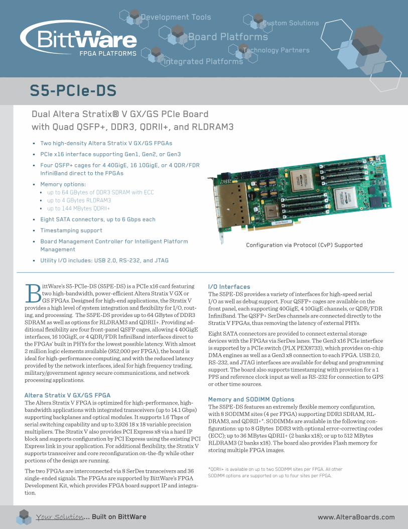
BittWare’s S5-PCIe-DS (S5PE-DS) is a PCIe x16 card featuring two high-bandwidth, power-efficient Altera Stratix V GX or GS FPGAs. Designed for high-end applications, the Stratix V
provides a high level of system integration and flexibility for I/O, rout-ing, and processing. The S5PE-DS provides up to 64 GBytes of DDR3 SDRAM as well as options for RLDRAM3 and QDRII+. Providing ad-ditional flexibility are four front-panel QSFP cages, allowing 4 40GigE interfaces, 16 10GigE, or 4 QDR/FDR InfiniBand interfaces direct to the FPGAs’ built in PHYs for the lowest possible latency. With almost 2 million logic elements available (952,000 per FPGA), the board is ideal for high-performance computing, and with the reduced latency provided by the network interfaces, ideal for high frequency trading, military/government agency secure communications, and network processing applications.
Altera Stratix V GX/GS FPGAThe Altera Stratix V FPGA is optimized for high-performance, high-bandwidth applications with integrated transceivers (up to 14.1 Gbps) supporting backplanes and optical modules. It supports 1.6 Tbps of serial switching capability and up to 3,926 18 x 18 variable precision multipliers. The Stratix V also provides PCI Express x8 via a hard IP block and supports configuration by PCI Express using the existing PCI Express link in your application. For additional flexibility, the Stratix V supports transceiver and core reconfiguration on-the-fly while other portions of the design are running.
The two FPGAs are interconnected via 8 SerDes transceivers and 36 single-ended signals. The FPGAs are supported by BittWare’s FPGA Development Kit, which provides FPGA board support IP and integra-tion.
I/O InterfacesThe S5PE-DS provides a variety of interfaces for high-speed serial I/O as well as debug support. Four QSFP+ cages are available on the front panel, each supporting 40GigE, 4 10GigE channels, or QDR/FDR InfiniBand. The QSFP+ SerDes channels are connected directly to the Stratix V FPGAs, thus removing the latency of external PHYs.
Eight SATA connectors are provided to connect external storage devices with the FPGAs via SerDes lanes. The Gen3 x16 PCIe interface is supported by a PCIe switch (PLX PEX8733), which provides on-chip DMA engines as well as a Gen3 x8 connection to each FPGA. USB 2.0, RS-232, and JTAG interfaces are available for debug and programming support. The board also supports timestamping with provision for a 1 PPS and reference clock input as well as RS-232 for connection to GPS or other time sources.
Memory and SODIMM OptionsThe S5PE-DS features an extremely flexible memory configuration, with 8 SODIMM sites (4 per FPGA) supporting DDR3 SDRAM, RL-DRAM3, and QDRII+*. SODIMMs are available in the following con-figurations: up to 8 GBytes DDR3 with optional error-correcting codes (ECC); up to 36 MBytes QDRII+ (2 banks x18); or up to 512 MBytes RLDRAM3 (2 banks x18). The board also provides Flash memory for storing multiple FPGA images.
*QDRII+isavailableonuptotwoSODIMMsitesperFPGA.AllotherSODIMMoptionsaresupportedonuptofoursitesperFPGA.
Dual Altera Stratix® V GX/GS PCIe Board with Quad QSFP+, DDR3, QDRII+, and RLDRAM3
Configuration via Protocol (CvP) Supported
www.AlteraBoards.comYour Solution... Built on BittWare
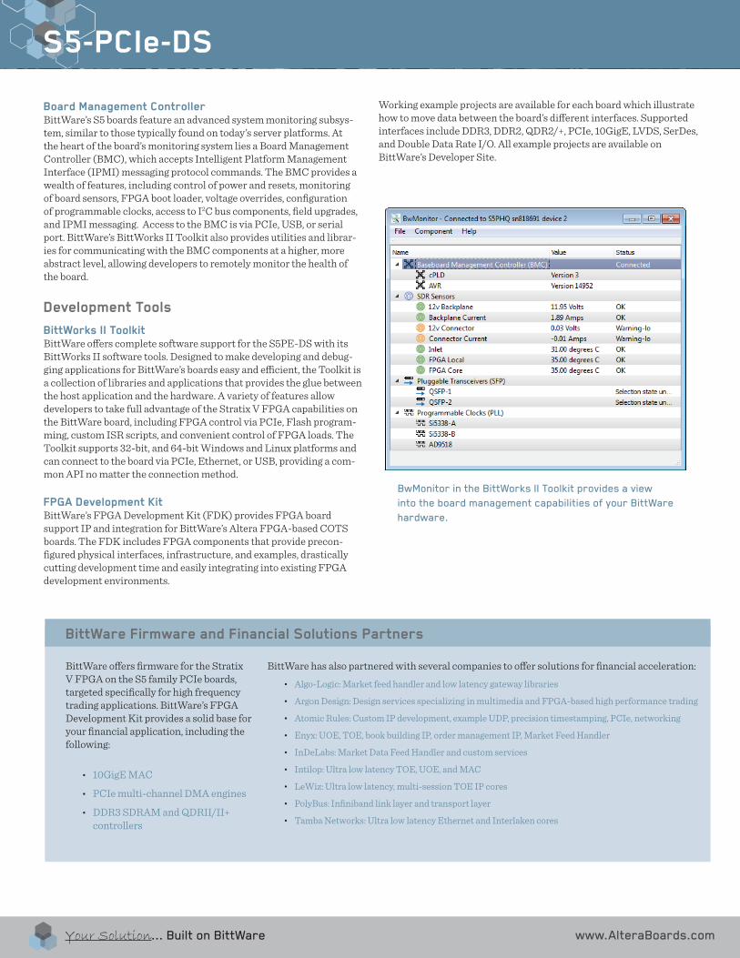
Board Management ControllerBittWare’s S5 boards feature an advanced system monitoring subsys-tem, similar to those typically found on today’s server platforms. At the heart of the board’s monitoring system lies a Board Management Controller (BMC), which accepts Intelligent Platform Management Interface (IPMI) messaging protocol commands. The BMC provides a wealth of features, including control of power and resets, monitoring of board sensors, FPGA boot loader, voltage overrides, configuration of programmable clocks, access to I2C bus components, field upgrades, and IPMI messaging. Access to the BMC is via PCIe, USB, or serial port. BittWare’s BittWorks II Toolkit also provides utilities and librar-ies for communicating with the BMC components at a higher, more abstract level, allowing developers to remotely monitor the health of the board.
Development ToolsBittWorks II ToolkitBittWare offers complete software support for the S5PE-DS with its BittWorks II software tools. Designed to make developing and debug-ging applications for BittWare’s boards easy and efficient, the Toolkit is a collection of libraries and applications that provides the glue between the host application and the hardware. A variety of features allow developers to take full advantage of the Stratix V FPGA capabilities on the BittWare board, including FPGA control via PCIe, Flash program-ming, custom ISR scripts, and convenient control of FPGA loads. The Toolkit supports 32-bit, and 64-bit Windows and Linux platforms and can connect to the board via PCIe, Ethernet, or USB, providing a com-mon API no matter the connection method.
FPGA Development KitBittWare’s FPGA Development Kit (FDK) provides FPGA board support IP and integration for BittWare’s Altera FPGA-based COTS boards. The FDK includes FPGA components that provide precon-figured physical interfaces, infrastructure, and examples, drastically cutting development time and easily integrating into existing FPGA development environments.
S5-PCIe-DS
Working example projects are available for each board which illustrate how to move data between the board’s different interfaces. Supported interfaces include DDR3, DDR2, QDR2/+, PCIe, 10GigE, LVDS, SerDes, and Double Data Rate I/O. All example projects are available on BittWare’s Developer Site.
BittWare Firmware and Financial Solutions Partners
BittWare offers firmware for the Stratix V FPGA on the S5 family PCIe boards, targeted specifically for high frequency trading applications. BittWare’s FPGA Development Kit provides a solid base for your financial application, including the following:
• 10GigE MAC
• PCIe multi-channel DMA engines
• DDR3 SDRAM and QDRII/II+ controllers
BittWare has also partnered with several companies to offer solutions for financial acceleration:
• Algo-Logic: Market feed handler and low latency gateway libraries
• Argon Design: Design services specializing in multimedia and FPGA-based high performance trading
• Atomic Rules: Custom IP development, example UDP, precision timestamping, PCIe, networking
• Enyx: UOE, TOE, book building IP, order management IP, Market Feed Handler
• InDeLabs: Market Data Feed Handler and custom services
• Intilop: Ultra low latency TOE, UOE, and MAC
• LeWiz: Ultra low latency, multi-session TOE IP cores
• PolyBus: Infiniband link layer and transport layer
• Tamba Networks: Ultra low latency Ethernet and Interlaken cores
BwMonitor in the BittWorks II Toolkit provides a view into the board management capabilities of your BittWare hardware.
www.AlteraBoards.comYour Solution... Built on BittWare
72
x36 SE ‘pins’
72
QSFP+/SFP+
QSFP+/SFP+4x
4x
4x SATA
16x PCIe
72
PCIe G3 Switch
FPGA AStratix V GX/GS
8x PCIe
Ext. Power
8x PCIe
8x
QSFP+/SFP+
QSFP+/SFP+ 4x
4x
72
204-pin SO-DIMM A4204-pin SO-DIMM A3
204-pin SO-DIMM A2204-pin SO-DIMM A1
(DDR3 up to 8GB w/ECC; RLDRAM3; QDRII+)
727272 72
204-pin SO-DIMM B4204-pin SO-DIMM B3
204-pin SO-DIMM B2204-pin SO-DIMM B1
(DDR3 up to 8GB w/ECC; RLDRAM3; QDRII+)
FPGA BStratix V GX/GS
4x SATA
FLASHLEDs
GPS/Time StampUSB Utility
Header
BMC
S5-PCIe-DS
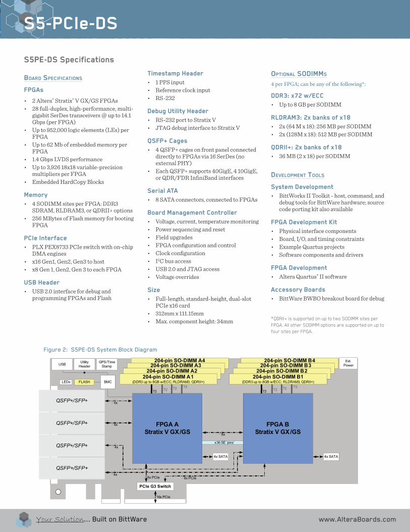
Figure 2: S5PE-DS System Block Diagram
S5PE-DS Specifications
Board SpecificationS
FPGAs
• 2 Altera® Stratix® V GX/GS FPGAs • 28 full-duplex, high-performance, multi-
gigabit SerDes transceivers @ up to 14.1 Gbps (per FPGA)
• Up to 952,000 logic elements (LEs) per FPGA
• Up to 62 Mb of embedded memory per FPGA
• 1.4 Gbps LVDS performance• Up to 3,926 18x18 variable-precision
multipliers per FPGA• Embedded HardCopy Blocks
Memory• 4 SODIMM sites per FPGA: DDR3
SDRAM, RLDRAM3, or QDRII+ options• 256 MBytes of Flash memory for booting
FPGA
PCIe Interface• PLX PEX8733 PCIe switch with on-chip
DMA engines• x16 Gen1, Gen2, Gen3 to host • x8 Gen 1, Gen2, Gen 3 to each FPGA
USB Header• USB 2.0 interface for debug and
programming FPGAs and Flash
Timestamp Header• 1 PPS input• Reference clock input• RS-232
Debug Utility Header• RS-232 port to Stratix V• JTAG debug interface to Stratix V
QSFP+ Cages• 4 QSFP+ cages on front panel connected
directly to FPGAs via 16 SerDes (no external PHY)
• Each QSFP+ supports 40GigE, 4 10GigE, or QDR/FDR InfiniBand interfaces
Serial ATA• 8 SATA connectors, connected to FPGAs
Board Management Controller• Voltage, current, temperature monitoring• Power sequencing and reset• Field upgrades• FPGA configuration and control• Clock configuration• I2C bus access • USB 2.0 and JTAG access • Voltage overrides
Size• Full-length, standard-height, dual-slot
PCIe x16 card• 312mm x 111.15mm• Max. component height: 34mm
optional SodiMMS
4 per FPGA; can be any of the following*:
DDR3: x72 w/ECC• Up to 8 GB per SODIMM
RLDRAM3: 2x banks of x18• 2x (64 M x 18): 256 MB per SODIMM• 2x (128M x 18): 512 MB per SODIMM
QDRII+: 2x banks of x18• 36 MB (2 x 18) per SODIMM
developMent toolS
System Development• BittWorks II Toolkit - host, command, and
debug tools for BittWare hardware; source code porting kit also available
FPGA Development Kit• Physical interface components• Board, I/O, and timing constraints• Example Quartus projects• Software components and drivers
FPGA Development• Altera Quartus® II software
Accessory Boards• BittWare BWBO breakout board for debug
*QDRII+issupportedonuptotwoSODIMMsitesperFPGA.AllotherSODIMMoptionsaresupportedonuptofoursitesperFPGA.
BittWare, Inc.45SouthMainStreet|Concord,NH03301USAPhone:603.226.0404E-mail:[email protected]
Your Solution... Built on BittWare
DS-S5PE-DS | Rev 2015.11.03 | November 2015
© BittWare, Inc. 2014Stratix V and Quartus II are registered trademarks of Altera Corp. All other products are the trademarks or registered trademarks of their respective holders.
S5PE-DS Ordering Options
S5PEDS-RW-AAAAABCC-DDEEFFGG-HHHHHIJJ-KKLLMMNN-OPQRS
RW Ruggedization
0U = Commercial (0C to 50C)*
AAAAA Stratix V A Family, HardIP, and Size
GXEA7 = Stratix V GXEA7†GXEAB = Stratix V GXEAB*GSMD5 = Stratix V GSMD5†GSED8 = Stratix V GSED8*
B Stratix V A GXB Speed
1 = 14.1 Gbps2 = 12.5 Gbps*‡3 = 8.5 Gbps
CC Stratix V A Temp/Speed
C1= Commercial Temperature Range, Speed Grade 1C2= Commercial Temperature Range, Speed Grade 2*C3= Commercial Temperature Range, Speed Grade 3
DD Cluster A SODIMM 1
00 = NoneD3 = DDR3 8GB x72*Q2 = QDRII+ 36MB 2x18 R2 = RLDRAM3 256MB 2x18 † R3 = RLDRAM3 512MB 2x18 †
EE Cluster A SODIMM 2
See options for “Cluster A SODIMM 1” (DD)
FF Cluster A SODIMM 3
00 = NoneD3 = DDR3 8GB x72*R2 = RLDRAM3 256MB 2x18 † R3 = RLDRAM3 512MB 2x18 †
GG Cluster A SODIMM 4
See options for “Cluster A SODIMM 3” (FF)
HHHHH Stratix V B Family, HardIP, and Size
See options for Stratix V A (AAAAA)
I Stratix V B GXB Speed
1 = 14.1 Gbps2 = 12.5 Gbps*‡3 = 8.5 Gbps
JJ Stratix V B Temp/Speed
C1= Commercial Temperature Range, Speed Grade 1C2= Commercial Temperature Range, Speed Grade 2*C3= Commercial Temperature Range, Speed Grade 3
KK Cluster B SODIMM 1
00 = NoneD3 = DDR3 8GB x72*Q2 = QDRII+ 36MB 2x18R2 = RLDRAM3 256MB 2x18 † R3 = RLDRAM3 512MB 2x18 †
LL Cluster B SODIMM 2
See options for “Cluster B SODIMM 1” (KK)
MM Cluster B SODIMM 3
00 = NoneD3 = DDR3 8GB x72*R2 = RLDRAM3 256MB 2x18 † R3 = RLDRAM3 512MB 2x18 †
NN Cluster B SODIMM 4
See options for “Cluster B SODIMM 3” (MM)
O Misc. Configuration
0 = Standard
P Oscillator
S = Standard*
Q Heatsink
B = FPGA Fansink*E = FPGA Heatsink
R Power Supply
R - Right-Angle Connector* V - Vertical Connector
S Envelope Assembly
6 = RoHS 6/6*
* Default † Contact BittWare for availability. ‡ On GXEAB devices, the Stratix V GXB speed is 11.2 Gbps. ** SODIMM site 1 supports QDRII+ SODIMM Q2SO-Cfg 1 only, and site 2 supports Q2SO-Cfg2 only.
• SODIMM Compatibility Table
SODIMM Site 1 Site 2 Site 3 Site 4
DDR3 Yes Yes Yes Yes
QDRII+ Yes** Yes** No †
RLDRAM Yes Yes Yes Yes

![cardchecklist 391105 script · CIR acp s5-21 ON S5-36 a SPR S5-41 s5-77 DR S5-58 a R S5-5 acp OSPR S5-22 ON S5-37 C] S5-42 acp DR CIR apR a R S5-27 C] PR S-5-88 a R S5-47 CIN s5-64](https://img.pdfslide.net/doc/110x75/5f34fee96b83591bd77e360b/cardchecklist-391105-script-cir-acp-s5-21-on-s5-36-a-spr-s5-41-s5-77-dr-s5-58-a.jpg)