Embed Size (px)
Citation preview
S905D3Quick Reference ManualRevision: 0.6Release Date: 2019–07–25
Prelim
inar
y Ver
sion
Confiden
tial f
or Wes
ion!
0.6 (2019–07–25) Amlogic Proprietary and ConfidentialCopyright © Amlogic. All rights reserved. i
Copyright©2019 Amlogic. All rights reserved. No part of this document may be reproduced, transmitted, tran-scribed, or translated into any language in any form or by any means without the written permission ofAmlogic.
Trademarks
, and other Amlogic icons are trademarks of Amlogic companies. All other trademarks andregistered trademarks are property of their respective holders.
DisclaimerAmlogic may make improvements and/or changes in this document or in the product described in thisdocument at any time.
This product is not intended for use in medical, life saving, or life sustaining applications.
Circuit diagrams and other information relating to products of Amlogic are included as a means of illus-trating typical applications. Consequently, complete information sufficient for production design is notnecessarily given. Amlogic makes no representations or warranties with respect to the accuracy orcompleteness of the contents presented in this document.
Contact Information●● Website: www.amlogic.com●● Pre-sales consultation: [email protected]●● Technical support: [email protected]
Prelim
inar
y Ver
sion
Confiden
tial f
or Wes
ion!
0.6 (2019–07–25) Amlogic Proprietary and ConfidentialCopyright © Amlogic. All rights reserved. ii
Revision History
Version 0.6(2019–07–23)This is the sixth release. Compare with the last version, the following part is added:●● 1
The following parts are modified:
Section Change Description
4.4, 4.5 Remove BT656 related signals.
Version 0.5(2019–05–14)This is the fifth release. Compare with the last version, the following part has been modified:
Section Change Description
2, 3 Remove DVP description, update Neural Network Processing Unit description
Version 0.4(2019–04–10)This is the forth release. Compare with last version the following part has been modified:
Section Change Description
3 Update SOC diagram
4.3 Update eARC_N, eARC_P description, remove VDDAO_0V8.
5.5.1 Update RPD, RPU, add Note
5.7.1 Add Note part for Table 5-1.
5.8 Updated Table 5-18
5.10 Update Note5, remove VDDAO_0V8
5.11 Update Table and Note part
Compare with last version the following topic is new added:●● 5.9
Version 0.3(2019-03-10)This is the third release. Compare with last version the following part has been modified:
Section Change Description
4.3, 5.2 Correct typo
5.3 Add note
S905D3 Quick Reference Manual Revision History
Prelim
inar
y Ver
sion
Confiden
tial f
or Wes
ion!
0.6 (2019–07–25) Amlogic Proprietary and ConfidentialCopyright © Amlogic. All rights reserved. iii
Version 0.2(2019-02-26)This is the second release. Compare with last version the following topic is new added:●● Pin Order●● Pin Description●● Recommended Operation Conditions●● Thermal Resistance●● Ethernet Timing
Compare with last version the following part has been modified:
Section Change Description
5.11 Add Power consumption data
Version 0.1(2019-02-21)This is the first release. Compare with last version the following part has been modified:
Section Change Description
5.5.1 Correct typo
Preliminary Version(2019-01-30)This is the preliminary release.
S905D3 Quick Reference Manual Revision History
Prelim
inar
y Ver
sion
Confiden
tial f
or Wes
ion!
S905D3 Quick Reference Manual Contents
0.6 (2019–07–25) Amlogic Proprietary and ConfidentialCopyright © Amlogic. All rights reserved. iv
Contents
Revision History ................................................................................................................................. ii1 About This Document....................................................................................................................12 General Description.......................................................................................................................23 Features Summary ........................................................................................................................34 Pinout Specification ......................................................................................................................8
4.1 Pin-Out Diagram (top view) ....................................................................................................84.2 Pin Order ...............................................................................................................................84.3 Pin Description ....................................................................................................................134.4 Pin Multiplexing Tables ........................................................................................................254.5 Signal Description................................................................................................................31
5 Operating Conditions ..................................................................................................................395.1 Absolute Maximum Ratings .................................................................................................395.2 Recommended Operating Conditions ..................................................................................395.3 Ripple Voltage Specifications...............................................................................................405.4 Thermal Resistance.............................................................................................................405.5 DC Electrical Characteristics................................................................................................41
5.5.1 Normal GPIO Specifications (For DIO_xmA) ..............................................................415.5.2 Open Drain GPIO Specifications (For DIO_OD) .........................................................425.5.3 DDR3/DDR3L/DDR4/LPDDR3/LPDDR4 SDRAM Specifications ................................43
5.6 Recommended Oscillator Electrical Characteristics..............................................................445.7 Timing Information ...............................................................................................................45
5.7.1 I2C Timing Specification ............................................................................................455.7.2 EMMC/SD Timing Specification .................................................................................465.7.3 NAND Timing Specification ........................................................................................515.7.4 SPICC Timing Specification .......................................................................................535.7.5 SPIFC Timing Specification........................................................................................545.7.6 Ethernet Timing Specification.....................................................................................555.7.7 Audio Timing Specification .........................................................................................585.7.8 PDM Timing Specification ..........................................................................................615.7.9 UART Timing Specification ........................................................................................62
5.8 Power On Config .................................................................................................................625.9 Power On Reset ..................................................................................................................635.10 Recommended Power on sequence...................................................................................645.11 Power Consumption...........................................................................................................655.12 Storage and Baking Conditions ..........................................................................................66
6 Mechanical Dimensions ..............................................................................................................67
Prelim
inar
y Ver
sion
Confiden
tial f
or Wes
ion!
0.6 (2019–07–25) Amlogic Proprietary and ConfidentialCopyright © Amlogic. All rights reserved. 1
1 About This DocumentThis document is applicable to S905D3 SoC series, please contact your Amlogic sales representativefor more detail.
S905D3 Quick Reference Manual 1 About This Document
Prelim
inar
y Ver
sion
Confiden
tial f
or Wes
ion!
0.6 (2019–07–25) Amlogic Proprietary and ConfidentialCopyright © Amlogic. All rights reserved. 2
2 General DescriptionS905D3 is an advanced application processor designed for hybrid OTT/IP Set Top Box (STB) andhigh-end media box applications. It integrates a powerful CPU/GPU subsystem, a powerful NPU(Neu-ral Network Processing Unit)Optional,a secured 4K video CODEC engine and a best-in-class HDR imageprocessing pipeline with all major peripherals to form the ultimate low power multimedia AP.
The main system CPU is a quad-core ARM Cortex-A55 CPU with unified L3 cache to improve systemperformance. In addition, the Cortex-A55 CPU includes the NEON SIMD co-processor to improve soft-ware media processing capability.
The graphic subsystem consists of two graphic engines and a flexible video/graphic output pipeline.The ARM G31 MP2 GPU handles all OpenGL ES 3.2 Vulkan 1.0 and OpenCL 2.0 graphic programs,while the 2.5D graphics processor handles additional scaling, alpha, rotation and color space conver-sion operations. Together, the CPU and GPU handle all operating system, networking, user-interfaceand gaming related tasks. The video output pipeline includes Dolby Visionoptional, HDR10+, HDR10,HLG and PRIME HDR processing, BT.709/BT.2020/BT.2100 processing, motion adaptive edge en-hancing de-interlacing, flexible programmable scalar, and many picture enhancement filters beforepassing the enhanced image to the video output ports.
Amlogic Video Engine (AVE-10) off-loads the Cortex-A55 CPUs from all video CODEC processing. Itincludes dedicated hardware video decoder and encoder. AVE-10 is capable of decoding 4Kx2K reso-lution video at 60fps with complete Trusted Video Path (TVP) for secure applications and supports fullformats including MVC, MPEG-1/2/4, VC-1/WMV, AVS, AVS+, AVS2 RealVideo, MJPEG streams,H.264, H265-10, VP9 and also JPEG pictures with no size limitation. The independent encoder is ableto encode in JPEG or H.265/H.264 up to 1080p at 60fps.
S905D3 integrates all standard audio/video input/output interfaces including a HDMI2.1 transmitterwith 3D, Dynamic HDR(w/EMP), CEC and HDCP2.2, ALLM(Auto Low Latency Mode) support,stereoaudio DAC, a CVBS output,4-lane MIPI DSI interface,2–lane MIPI CSI interface, multiple TDM, PCM,I2S and SPDIF digital audio input/output interfaces, and 8 channel far-field PDM digital microphone(DMIC) inputs. It also has build-in Voice Activity Detection(VAD)module for ultra-low power operationsduring system standby.
S905D3 also integrates a set of functional blocks for digital TV broadcasting streams. The built-in twodemux can process the TV streams from the serial and paralleltransport stream input interface, whichcan connect to external tuner/demodulator.
The processor has rich advanced network and peripheral interfaces, including a 10/100/1000M Ether-net MAC with RGMII, 10/100M Ethernet PHY,a set of multi-PHY for USB2, USB3 and PCIe,and multi-ple SDIO/SD card controllers, UART, I2C, high-speed SPI and PWMs.
Standard development environment utilizing GNU/GCC Android tool chain is supported. Please con-tact your AMLOGIC sales representative for more information.
S905D3 Quick Reference Manual 2 General Description
Prelim
inar
y Ver
sion
Confiden
tial f
or Wes
ion!
0.6 (2019–07–25) Amlogic Proprietary and ConfidentialCopyright © Amlogic. All rights reserved. 3
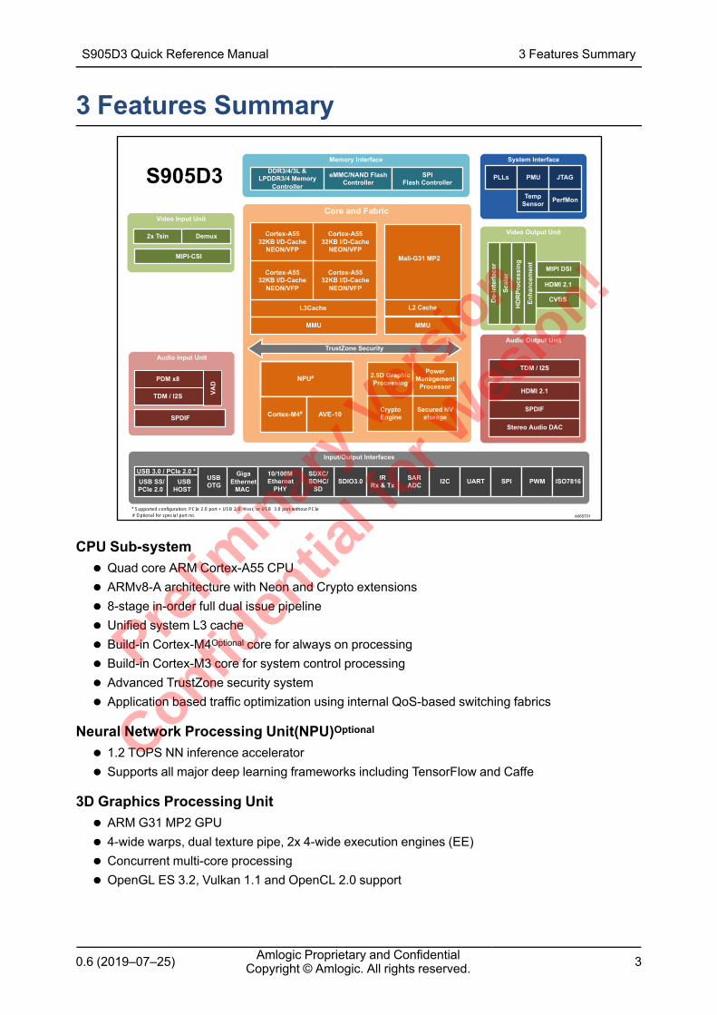
3 Features Summary
CPU Sub-system●● Quad core ARM Cortex-A55 CPU●● ARMv8-A architecture with Neon and Crypto extensions●● 8-stage in-order full dual issue pipeline●● Unified system L3 cache●● Build-in Cortex-M4Optional core for always on processing●● Build-in Cortex-M3 core for system control processing●● Advanced TrustZone security system●● Application based traffic optimization using internal QoS-based switching fabrics
Neural Network Processing Unit(NPU)Optional●● 1.2 TOPS NN inference accelerator●● Supports all major deep learning frameworks including TensorFlow and Caffe
3D Graphics Processing Unit●● ARM G31 MP2 GPU●● 4-wide warps, dual texture pipe, 2x 4-wide execution engines (EE)●● Concurrent multi-core processing●● OpenGL ES 3.2, Vulkan 1.1 and OpenCL 2.0 support
S905D3Memory Interface System Interface
Video Output Unit
De-
inte
rlace
r
Scal
ar
HD
RPr
oces
sing
HDMI 2.1
Core and Fabric
TrustZone Security
Input/Output Interfaces
USB HOST
USB OTG SDIO3.0 I2C UART SPI PWMSAR
ADC
SDXC/SDHC/
SD
L3Cache
MMU
Audio Output Unit
TDM / I2S
HDMI 2.1
SPDIF
IR Rx & Tx
PLLs PMU JTAG
TempSensor PerfMon
Audio Input Unit
SPDIF
DDR3/4/3L & LPDDR3/4 Memory
Controller
eMMC/NAND Flash Controller
SPI Flash Controller
2.5D GraphicProcessing
CryptoEngine
Secured NV storage
Power Management
Processor
10/100M Ethernet
PHY
CVBS
TDM / I2S
Cortex-A5532KB I/D-Cache
NEON/VFP
Cortex-A5532KB I/D-Cache
NEON/VFP
Cortex-A5532KB I/D-Cache
NEON/VFP
Cortex-A5532KB I/D-Cache
NEON/VFP
PDM x8
Stereo Audio DAC
Enha
ncem
ent
L2 Cache
MMU
Mali-G31 MP2
Video Input Unit
2x Tsin Demux
MIPI-CSI
MIPI DSI
Giga Ethernet
MACUSB SS/ PCIe 2.0
USB 3.0 / PCIe 2.0 *ISO7816
* Supported configuration: PCIe 2.0 port + USB 2.0 Host, or USB 3.0 port without PCIeA06ST01
NPU#
Cortex-M4# AVE-10
VAD
# Optional for special part no.
S905D3 Quick Reference Manual 3 Features Summary
Prelim
inar
y Ver
sion
Confiden
tial f
or Wes
ion!
0.6 (2019–07–25) Amlogic Proprietary and ConfidentialCopyright © Amlogic. All rights reserved. 4
2.5D Graphics Processor●● Fast bitblt engine with dual inputs and single output●● Programmable raster operations (ROP)●● Programmable polyphase scaling filter●● Supports multiple video formats 4:2:0, 4:2:2 and 4:4:4 and multiple pixel formats (8/16/24/32 bitsgraphics layer)
●● Fast color space conversion●● Advanced anti-flickering filter
Crypto Engine●● AES/ block cipher with 128/256 bits keys, standard 16 bytes block size and streaming ECB,CBC and CTR modes
●● TDES block cipher with ECB and CBC modes supporting 64 bits key for DES and 192 bits keyfor 3DES
●● SM4 block cipher with ECB, CBC, CTR modes●● Hardware crypto key-ladder operation and DVB-CSA for transport stream encryption●● Built-in hardware True Random Number Generator (TRNG), CRC and SHA-1/SHA-2/HMACSHA engine
Video/Picture CODEC●● Amlogic Video Engine (AVE) with dedicated hardware decoders and encoders●● Support multi-video decoder up to 4x1080P@60fps●● Supports multiple “secured” video decoding sessions and simultaneous decoding and encoding●● Video/Picture Decoding
− VP9 Profile-2 up to 4Kx2K@60fps− H.265 HEVC [email protected] up to 4Kx2K@60fps− AVS2-P2 Profile up to 4Kx2K@60fps− H.264 AVC [email protected] up to 4Kx2K@30fps− MPEG-4 ASP@L5 up to 1080P@60fps (ISO-14496)− WMV/VC-1 SP/MP/AP up to 1080P@60fps− AVS-P16(AVS+) /AVS-P2 JiZhun Profile up to 1080P@60fps− MPEG-2 MP/HL up to 1080P@60fps (ISO-13818)− MPEG-1 MP/HL up to 1080P@60fps (ISO-11172)− RealVideo 8/9/10 up to 1080P@60fps− Multiple language and multiple format sub-title video support− MJPEG and JPEG unlimited pixel resolution decoding (ISO/IEC-10918)− Supports JPEG thumbnail, scaling, rotation and transition effects− Supports *.mkv,*.wmv,*.mpg, *.mpeg, *.dat, *.avi, *.mov, *.iso, *.mp4, *.rm and *.jpg fileformats
●● Video/Picture Encoding− Independent JPEG and H.264 encoder with configurable performance/bit-rate− JPEG image encoding− H.265/H.264 video encoding up to 1080P@60fps with low latency
S905D3 Quick Reference Manual 3 Features Summary
Prelim
inar
y Ver
sion
Confiden
tial f
or Wes
ion!
0.6 (2019–07–25) Amlogic Proprietary and ConfidentialCopyright © Amlogic. All rights reserved. 5
8th Generation Advanced Amlogic TruLife Image Engine●● Supports Dolby Visionoptional, HDR10+, HDR10, HLG and Technicolor HDR processing●● Motion compensated noise reduction and 3D digital noise reduction for random noise●● Block noise, mosquito noise, spatial noise, contour noise reduction●● Motion compensated and motion adaptive de-interlacer●● Edge interpolation with low angle protection and processing●● 3:2/2:2 pulldown and Video on Film (VOF) detection and processing●● Smart sharpness with SuperScaler technology including de-contouring, de-ring, LTI, CTI, de-jaggy, peaking
●● Dynamic non-Linear contrast enhancement●● All dimension multiple regions smart color management including blue/green extension, flesh-tone correction, wider gamut for video
●● 2 video planes and 3 graphics planes hardware composer●● Independent HDR re-mapping of video and graphic layer
Video Input/Output Interface●● MIPI-CSI camera interface with 2 lanes●● Built-in HDMI 2.1 transmitter including both controller and PHY supporting eARC,CEC, DynamicHDR and HDCP 2.2, 4Kx2K@60 max resolution output
●● CVBS 480i/576i standard definition output●● Supports all standard SD/HD/FHD video output formats: 480i/p, 576i/p, 720p, 1080i/p and4Kx2K
●● 4-lane MIPI DSI interface, resolution up to 1920*1080
Audio Decoder and Input/Output●● Supports MP3, AAC, WMA, RM, FLAC, Ogg,Dolby DigitalOptional, Dolby Digital PlusOptional, DTSOp-
tional and programmable with 7.1/5.1 down-mixing●● Low-power VAD●● Built-in serial digital audio SPDIF/IEC958 input/output and PCM input/output, SPDIF supports192KHz 16/24/32bit stereo
●● 3 built-in TDM/PCM/I2S ports with TDM/PCM mode up to 384kHz x 32bits x 16ch or 96kHz x32bits x 32ch and I2S mode up to 384kHz x 32bits x 16ch
●● Digital microphone PDM input with programmable CIC, LPF & HPF, support up to 8 DMICs●● Built-in stereo audio DAC●● Supports concurrent dual audio stereo channel output with combination of analog+PCM or I2S+PCM
Memory and Storage Interface●● 32-bit DRAM memory interface with dual ranks and max 4GB total address space●● Compatible with JEDEC standard DDR3-2133 /DDR3L-2133 /DDR4-3200 /LPDDR3-2133/LPDDR4-3200 SDRAM
●● Supports SLC/MLC/TLC NAND Flash with 60-bit ECC, compatible to Toshiba toggle mode in ad-dition to ONFI 2.2
●● SDSC/SDHC/SDXC card and SDIO interface with 1-bit and 4-bit data bus width supporting specversion 2.x/3.x/4.x DS/HS modes up to UHS-I SDR104
●● eMMC and MMC card interface with 1/4/8-bit data bus width fully supporting spec version 5.0HS400
●● Supports serial 1, 2 or 4-bit NOR Flash via SPI interface
S905D3 Quick Reference Manual 3 Features Summary
Prelim
inar
y Ver
sion
Confiden
tial f
or Wes
ion!
0.6 (2019–07–25) Amlogic Proprietary and ConfidentialCopyright © Amlogic. All rights reserved. 6
●● Built-in 4k bits One-Time-Programming memory for key storage
Network●● Integrated IEEE 802.3 10/100/1000M Ethernet MAC with RGMII interface●● Integrate 10/100M Ethernet PHY interface●● WiFi/IEEE802.11 & Bluetooth supporting via PCIE/SDIO /USB/UART/PCM●● Network interface optimized for mixed WIFI and BT traffic
Digital Television Interface●● One serial and one parallel Transport stream (TS) input interface with built-in demux processorfor connecting to external digital TV tuner/demodulator
●● Built-in PWM, I2C and SPI interfaces to control tuner and demodulator●● Integrated ISO 7816 smart card controller
Integrated I/O Controllers and Interfaces●● One USB XHCI OTG 2.0 port●● One USB SS and PCIE 2.0 combo port up to 5Gbps, which supports 2 configurations:
− 1 USB 2.0 Host + 1 PCIe− 1 USB3.0 (No PCIe)
●● Multiple PWM, UART, I2C and SPI interface with slave select●● Programmable IR remote input/output controllers●● Built-in 10bit SAR ADC with 4 input channels●● A set of General Purpose IOs with built-in pull up and pull down
System, Peripherals and Misc. Interfaces●● Integrated general purpose timers, counters, DMA controllers●● 24 MHz crystal input●● Embedded debug interface using ICE/JTAG●● Integrated Power On Reset(POR) module
Power Management●● Multiple internal power domains controlled by software●● Multiple sleep modes for CPU, system, DRAM, etc.●● Multiple internal PLLs for DVFS operation●● Multi-voltage I/O design for 1.8V and 3.3V●● Power management auxiliary processor in a dedicated always-on (AO) power domain that cancommunicate with an external PMIC
Security●● Trustzone based Trusted Execution Environment (TEE)●● Secured boot, encrypted OTP, encrypted DRAM with memory integrity checker, hardware keyladder and internal control buses and storage
●● Separated secure/non-secure Entropy true RNG●● Pre-region/ID memory security control and electric fence●● Hardware based Trusted Video Path (TVP) , video watermarking and secured contents (needsSecureOS software)
●● Secured IO and secured clock
S905D3 Quick Reference Manual 3 Features Summary
Prelim
inar
y Ver
sion
Confiden
tial f
or Wes
ion!
0.6 (2019–07–25) Amlogic Proprietary and ConfidentialCopyright © Amlogic. All rights reserved. 7
Package●● FCBGA, 16.1mmx14.3mm, 0.6mm ball pitch, RoHS compliant
S905D3 Quick Reference Manual 3 Features Summary
Prelim
inar
y Ver
sion
Confiden
tial f
or Wes
ion!
0.6 (2019–07–25) Amlogic Proprietary and ConfidentialCopyright © Amlogic. All rights reserved. 8
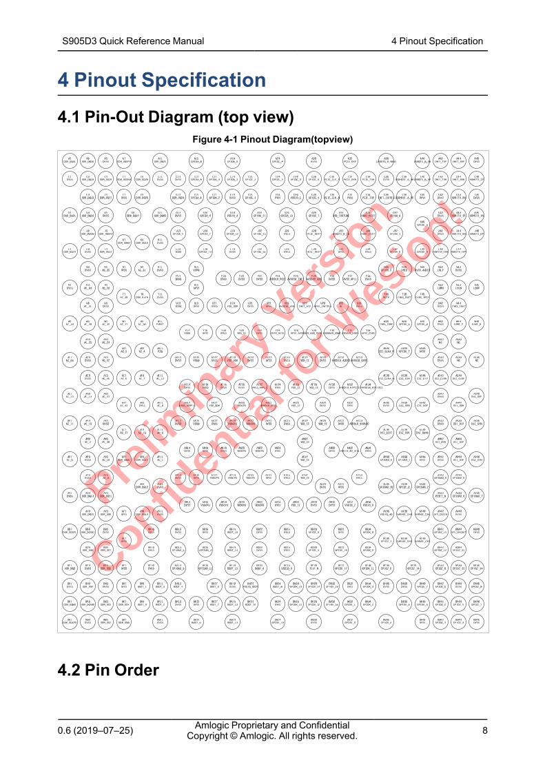
4 Pinout Specification4.1 Pin-Out Diagram (top view)
Figure 4-1 Pinout Diagram(topview)
4.2 Pin Order
S905D3 Quick Reference Manual 4 Pinout Specification
Prelim
inar
y Ver
sion
Confiden
tial f
or Wes
ion!
0.6 (2019–07–25) Amlogic Proprietary and ConfidentialCopyright © Amlogic. All rights reserved. 9
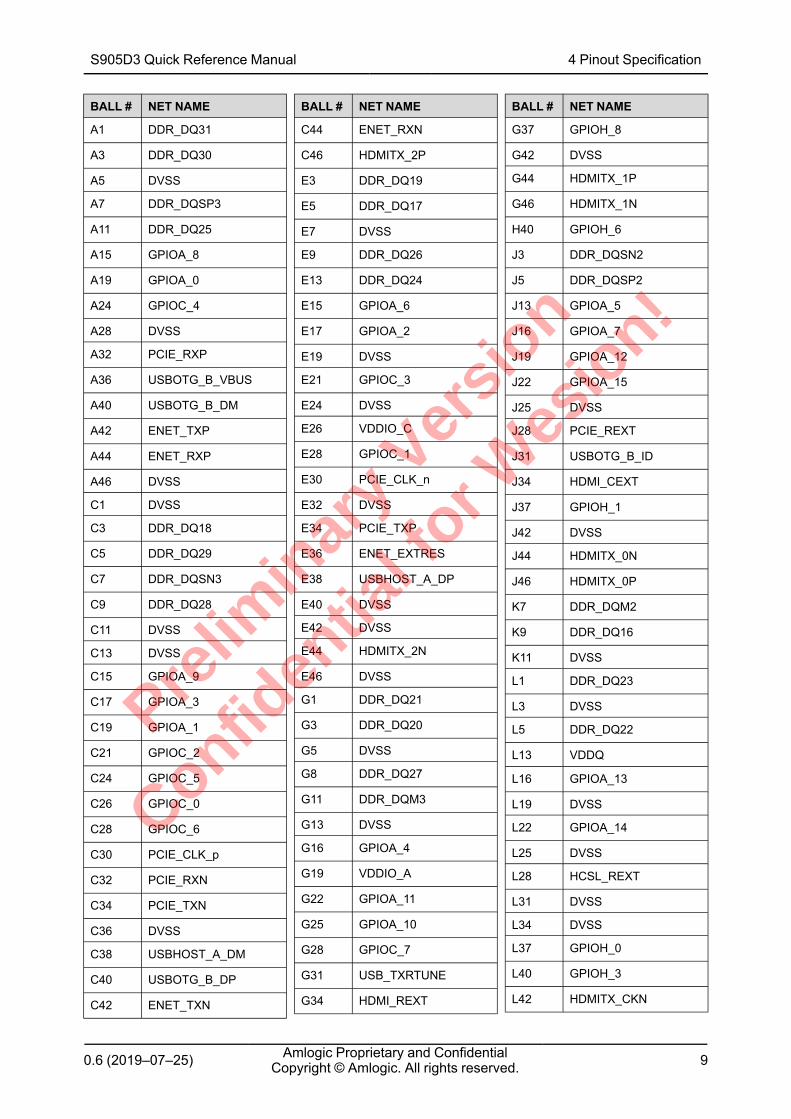
BALL # NET NAME
A1 DDR_DQ31
A3 DDR_DQ30
A5 DVSS
A7 DDR_DQSP3
A11 DDR_DQ25
A15 GPIOA_8
A19 GPIOA_0
A24 GPIOC_4
A28 DVSS
A32 PCIE_RXP
A36 USBOTG_B_VBUS
A40 USBOTG_B_DM
A42 ENET_TXP
A44 ENET_RXP
A46 DVSS
C1 DVSS
C3 DDR_DQ18
C5 DDR_DQ29
C7 DDR_DQSN3
C9 DDR_DQ28
C11 DVSS
C13 DVSS
C15 GPIOA_9
C17 GPIOA_3
C19 GPIOA_1
C21 GPIOC_2
C24 GPIOC_5
C26 GPIOC_0
C28 GPIOC_6
C30 PCIE_CLK_p
C32 PCIE_RXN
C34 PCIE_TXN
C36 DVSS
C38 USBHOST_A_DM
C40 USBOTG_B_DP
C42 ENET_TXN
BALL # NET NAME
C44 ENET_RXN
C46 HDMITX_2P
E3 DDR_DQ19
E5 DDR_DQ17
E7 DVSS
E9 DDR_DQ26
E13 DDR_DQ24
E15 GPIOA_6
E17 GPIOA_2
E19 DVSS
E21 GPIOC_3
E24 DVSS
E26 VDDIO_C
E28 GPIOC_1
E30 PCIE_CLK_n
E32 DVSS
E34 PCIE_TXP
E36 ENET_EXTRES
E38 USBHOST_A_DP
E40 DVSS
E42 DVSS
E44 HDMITX_2N
E46 DVSS
G1 DDR_DQ21
G3 DDR_DQ20
G5 DVSS
G8 DDR_DQ27
G11 DDR_DQM3
G13 DVSS
G16 GPIOA_4
G19 VDDIO_A
G22 GPIOA_11
G25 GPIOA_10
G28 GPIOC_7
G31 USB_TXRTUNE
G34 HDMI_REXT
BALL # NET NAME
G37 GPIOH_8
G42 DVSS
G44 HDMITX_1P
G46 HDMITX_1N
H40 GPIOH_6
J3 DDR_DQSN2
J5 DDR_DQSP2
J13 GPIOA_5
J16 GPIOA_7
J19 GPIOA_12
J22 GPIOA_15
J25 DVSS
J28 PCIE_REXT
J31 USBOTG_B_ID
J34 HDMI_CEXT
J37 GPIOH_1
J42 DVSS
J44 HDMITX_0N
J46 HDMITX_0P
K7 DDR_DQM2
K9 DDR_DQ16
K11 DVSS
L1 DDR_DQ23
L3 DVSS
L5 DDR_DQ22
L13 VDDQ
L16 GPIOA_13
L19 DVSS
L22 GPIOA_14
L25 DVSS
L28 HCSL_REXT
L31 DVSS
L34 DVSS
L37 GPIOH_0
L40 GPIOH_3
L42 HDMITX_CKN
S905D3 Quick Reference Manual 4 Pinout Specification
Prelim
inar
y Ver
sion
Confiden
tial f
or Wes
ion!
0.6 (2019–07–25) Amlogic Proprietary and ConfidentialCopyright © Amlogic. All rights reserved. 10
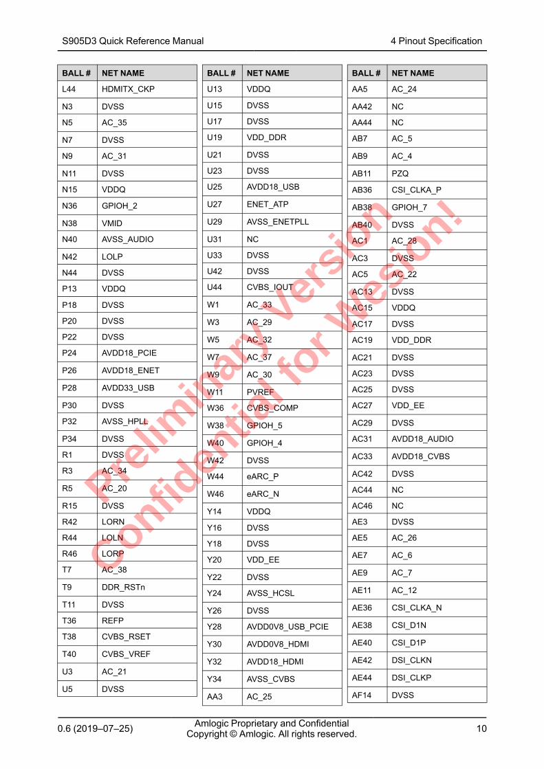
BALL # NET NAME
L44 HDMITX_CKP
N3 DVSS
N5 AC_35
N7 DVSS
N9 AC_31
N11 DVSS
N15 VDDQ
N36 GPIOH_2
N38 VMID
N40 AVSS_AUDIO
N42 LOLP
N44 DVSS
P13 VDDQ
P18 DVSS
P20 DVSS
P22 DVSS
P24 AVDD18_PCIE
P26 AVDD18_ENET
P28 AVDD33_USB
P30 DVSS
P32 AVSS_HPLL
P34 DVSS
R1 DVSS
R3 AC_34
R5 AC_20
R15 DVSS
R42 LORN
R44 LOLN
R46 LORP
T7 AC_38
T9 DDR_RSTn
T11 DVSS
T36 REFP
T38 CVBS_RSET
T40 CVBS_VREF
U3 AC_21
U5 DVSS
BALL # NET NAME
U13 VDDQ
U15 DVSS
U17 DVSS
U19 VDD_DDR
U21 DVSS
U23 DVSS
U25 AVDD18_USB
U27 ENET_ATP
U29 AVSS_ENETPLL
U31 NC
U33 DVSS
U42 DVSS
U44 CVBS_IOUT
W1 AC_33
W3 AC_29
W5 AC_32
W7 AC_37
W9 AC_30
W11 PVREF
W36 CVBS_COMP
W38 GPIOH_5
W40 GPIOH_4
W42 DVSS
W44 eARC_P
W46 eARC_N
Y14 VDDQ
Y16 DVSS
Y18 DVSS
Y20 VDD_EE
Y22 DVSS
Y24 AVSS_HCSL
Y26 DVSS
Y28 AVDD0V8_USB_PCIE
Y30 AVDD0V8_HDMI
Y32 AVDD18_HDMI
Y34 AVSS_CVBS
AA3 AC_25
BALL # NET NAME
AA5 AC_24
AA42 NC
AA44 NC
AB7 AC_5
AB9 AC_4
AB11 PZQ
AB36 CSI_CLKA_P
AB38 GPIOH_7
AB40 DVSS
AC1 AC_28
AC3 DVSS
AC5 AC_22
AC13 DVSS
AC15 VDDQ
AC17 DVSS
AC19 VDD_DDR
AC21 DVSS
AC23 DVSS
AC25 DVSS
AC27 VDD_EE
AC29 DVSS
AC31 AVDD18_AUDIO
AC33 AVDD18_CVBS
AC42 DVSS
AC44 NC
AC46 NC
AE3 DVSS
AE5 AC_26
AE7 AC_6
AE9 AC_7
AE11 AC_12
AE36 CSI_CLKA_N
AE38 CSI_D1N
AE40 CSI_D1P
AE42 DSI_CLKN
AE44 DSI_CLKP
AF14 DVSS
S905D3 Quick Reference Manual 4 Pinout Specification
Prelim
inar
y Ver
sion
Confiden
tial f
or Wes
ion!
0.6 (2019–07–25) Amlogic Proprietary and ConfidentialCopyright © Amlogic. All rights reserved. 11
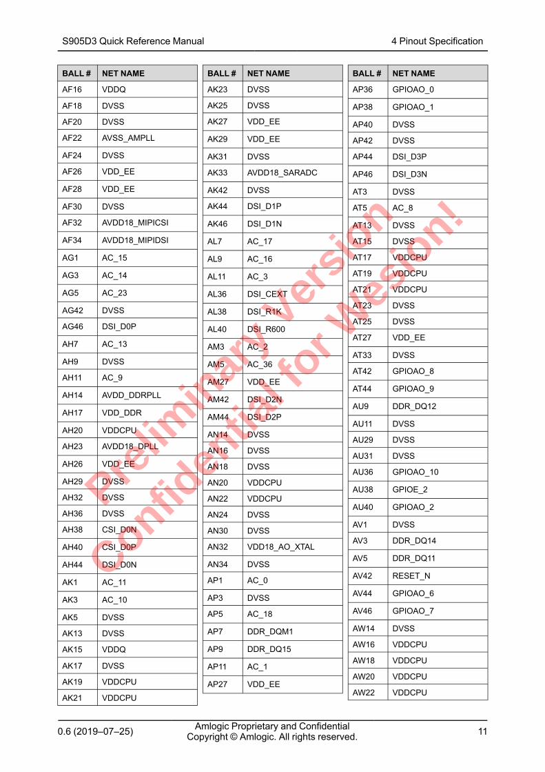
BALL # NET NAME
AF16 VDDQ
AF18 DVSS
AF20 DVSS
AF22 AVSS_AMPLL
AF24 DVSS
AF26 VDD_EE
AF28 VDD_EE
AF30 DVSS
AF32 AVDD18_MIPICSI
AF34 AVDD18_MIPIDSI
AG1 AC_15
AG3 AC_14
AG5 AC_23
AG42 DVSS
AG46 DSI_D0P
AH7 AC_13
AH9 DVSS
AH11 AC_9
AH14 AVDD_DDRPLL
AH17 VDD_DDR
AH20 VDDCPU
AH23 AVDD18_DPLL
AH26 VDD_EE
AH29 DVSS
AH32 DVSS
AH36 DVSS
AH38 CSI_D0N
AH40 CSI_D0P
AH44 DSI_D0N
AK1 AC_11
AK3 AC_10
AK5 DVSS
AK13 DVSS
AK15 VDDQ
AK17 DVSS
AK19 VDDCPU
AK21 VDDCPU
BALL # NET NAME
AK23 DVSS
AK25 DVSS
AK27 VDD_EE
AK29 VDD_EE
AK31 DVSS
AK33 AVDD18_SARADC
AK42 DVSS
AK44 DSI_D1P
AK46 DSI_D1N
AL7 AC_17
AL9 AC_16
AL11 AC_3
AL36 DSI_CEXT
AL38 DSI_R1K
AL40 DSI_R600
AM3 AC_2
AM5 AC_36
AM27 VDD_EE
AM42 DSI_D2N
AM44 DSI_D2P
AN14 DVSS
AN16 DVSS
AN18 DVSS
AN20 VDDCPU
AN22 VDDCPU
AN24 DVSS
AN30 DVSS
AN32 VDD18_AO_XTAL
AN34 DVSS
AP1 AC_0
AP3 DVSS
AP5 AC_18
AP7 DDR_DQM1
AP9 DDR_DQ15
AP11 AC_1
AP27 VDD_EE
BALL # NET NAME
AP36 GPIOAO_0
AP38 GPIOAO_1
AP40 DVSS
AP42 DVSS
AP44 DSI_D3P
AP46 DSI_D3N
AT3 DVSS
AT5 AC_8
AT13 DVSS
AT15 DVSS
AT17 VDDCPU
AT19 VDDCPU
AT21 VDDCPU
AT23 DVSS
AT25 DVSS
AT27 VDD_EE
AT33 DVSS
AT42 GPIOAO_8
AT44 GPIOAO_9
AU9 DDR_DQ12
AU11 DVSS
AU29 DVSS
AU31 DVSS
AU36 GPIOAO_10
AU38 GPIOE_2
AU40 GPIOAO_2
AV1 DVSS
AV3 DDR_DQ14
AV5 DDR_DQ11
AV42 RESET_N
AV44 GPIOAO_6
AV46 GPIOAO_7
AW14 DVSS
AW16 VDDCPU
AW18 VDDCPU
AW20 VDDCPU
AW22 VDDCPU
S905D3 Quick Reference Manual 4 Pinout Specification
Prelim
inar
y Ver
sion
Confiden
tial f
or Wes
ion!
0.6 (2019–07–25) Amlogic Proprietary and ConfidentialCopyright © Amlogic. All rights reserved. 12
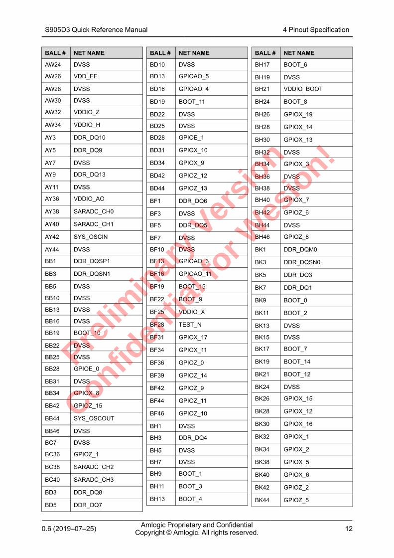
BALL # NET NAME
AW24 DVSS
AW26 VDD_EE
AW28 DVSS
AW30 DVSS
AW32 VDDIO_Z
AW34 VDDIO_H
AY3 DDR_DQ10
AY5 DDR_DQ9
AY7 DVSS
AY9 DDR_DQ13
AY11 DVSS
AY36 VDDIO_AO
AY38 SARADC_CH0
AY40 SARADC_CH1
AY42 SYS_OSCIN
AY44 DVSS
BB1 DDR_DQSP1
BB3 DDR_DQSN1
BB5 DVSS
BB10 DVSS
BB13 DVSS
BB16 DVSS
BB19 BOOT_10
BB22 DVSS
BB25 DVSS
BB28 GPIOE_0
BB31 DVSS
BB34 GPIOX_8
BB42 GPIOZ_15
BB44 SYS_OSCOUT
BB46 DVSS
BC7 DVSS
BC36 GPIOZ_1
BC38 SARADC_CH2
BC40 SARADC_CH3
BD3 DDR_DQ8
BD5 DDR_DQ7
BALL # NET NAME
BD10 DVSS
BD13 GPIOAO_5
BD16 GPIOAO_4
BD19 BOOT_11
BD22 DVSS
BD25 DVSS
BD28 GPIOE_1
BD31 GPIOX_10
BD34 GPIOX_9
BD42 GPIOZ_12
BD44 GPIOZ_13
BF1 DDR_DQ6
BF3 DVSS
BF5 DDR_DQ5
BF7 DVSS
BF10 DVSS
BF13 GPIOAO_3
BF16 GPIOAO_11
BF19 BOOT_15
BF22 BOOT_9
BF25 VDDIO_X
BF28 TEST_N
BF31 GPIOX_17
BF34 GPIOX_11
BF36 GPIOZ_0
BF39 GPIOZ_14
BF42 GPIOZ_9
BF44 GPIOZ_11
BF46 GPIOZ_10
BH1 DVSS
BH3 DDR_DQ4
BH5 DVSS
BH7 DVSS
BH9 BOOT_1
BH11 BOOT_3
BH13 BOOT_4
BALL # NET NAME
BH17 BOOT_6
BH19 DVSS
BH21 VDDIO_BOOT
BH24 BOOT_8
BH26 GPIOX_19
BH28 GPIOX_14
BH30 GPIOX_13
BH32 DVSS
BH34 GPIOX_3
BH36 DVSS
BH38 DVSS
BH40 GPIOX_7
BH42 GPIOZ_6
BH44 DVSS
BH46 GPIOZ_8
BK1 DDR_DQM0
BK3 DDR_DQSN0
BK5 DDR_DQ3
BK7 DDR_DQ1
BK9 BOOT_0
BK11 BOOT_2
BK13 DVSS
BK15 DVSS
BK17 BOOT_7
BK19 BOOT_14
BK21 BOOT_12
BK24 DVSS
BK26 GPIOX_15
BK28 GPIOX_12
BK30 GPIOX_16
BK32 GPIOX_1
BK34 GPIOX_2
BK38 GPIOX_5
BK40 GPIOX_6
BK42 GPIOZ_2
BK44 GPIOZ_5
S905D3 Quick Reference Manual 4 Pinout Specification
Prelim
inar
y Ver
sion
Confiden
tial f
or Wes
ion!
0.6 (2019–07–25) Amlogic Proprietary and ConfidentialCopyright © Amlogic. All rights reserved. 13
BALL # NET NAME
BK46 GPIOZ_7
BM1 DDR_DQSP0
BM3 DVSS
BM5 DDR_DQ2
BM7 DDR_DQ0
BM11 DVSS
BALL # NET NAME
BM15 BOOT_5
BM19 BOOT_13
BM24 GPIOX_18
BM28 DVSS
BM32 GPIOX_0
BM36 GPIOX_4
BALL # NET NAME
BM40 DVSS
BM42 GPIOZ_3
BM44 GPIOZ_4
BM46 DVSS
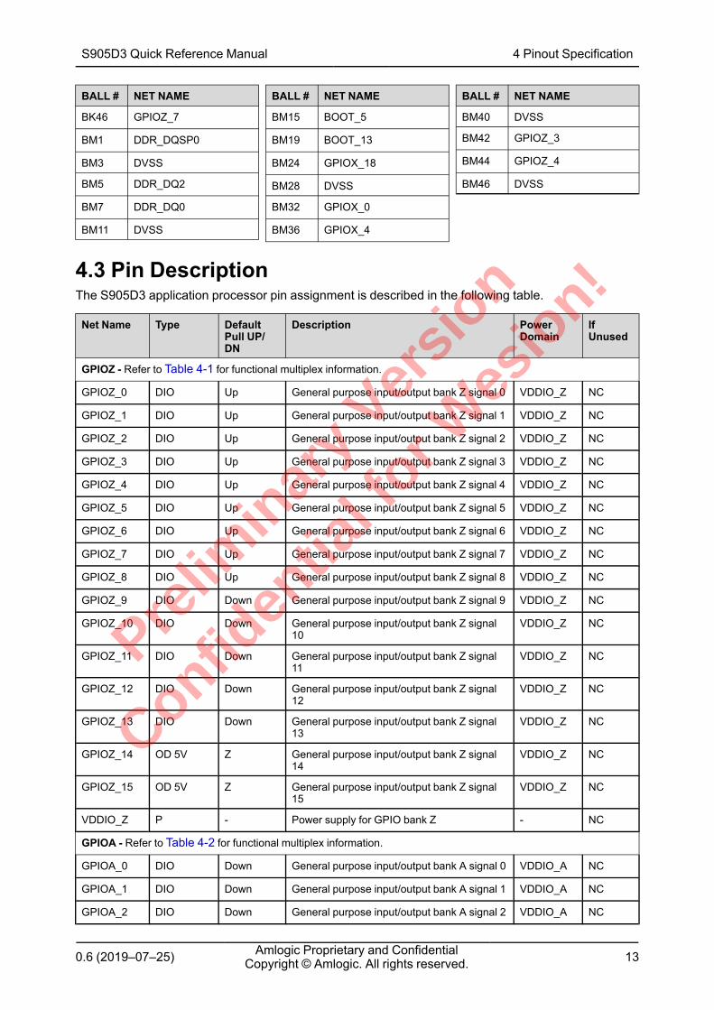
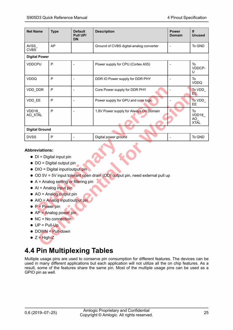
4.3 Pin DescriptionThe S905D3 application processor pin assignment is described in the following table.
Net Name Type DefaultPull UP/DN
Description PowerDomain
IfUnused
GPIOZ - Refer to Table 4-1 for functional multiplex information.
GPIOZ_0 DIO Up General purpose input/output bank Z signal 0 VDDIO_Z NC
GPIOZ_1 DIO Up General purpose input/output bank Z signal 1 VDDIO_Z NC
GPIOZ_2 DIO Up General purpose input/output bank Z signal 2 VDDIO_Z NC
GPIOZ_3 DIO Up General purpose input/output bank Z signal 3 VDDIO_Z NC
GPIOZ_4 DIO Up General purpose input/output bank Z signal 4 VDDIO_Z NC
GPIOZ_5 DIO Up General purpose input/output bank Z signal 5 VDDIO_Z NC
GPIOZ_6 DIO Up General purpose input/output bank Z signal 6 VDDIO_Z NC
GPIOZ_7 DIO Up General purpose input/output bank Z signal 7 VDDIO_Z NC
GPIOZ_8 DIO Up General purpose input/output bank Z signal 8 VDDIO_Z NC
GPIOZ_9 DIO Down General purpose input/output bank Z signal 9 VDDIO_Z NC
GPIOZ_10 DIO Down General purpose input/output bank Z signal10
VDDIO_Z NC
GPIOZ_11 DIO Down General purpose input/output bank Z signal11
VDDIO_Z NC
GPIOZ_12 DIO Down General purpose input/output bank Z signal12
VDDIO_Z NC
GPIOZ_13 DIO Down General purpose input/output bank Z signal13
VDDIO_Z NC
GPIOZ_14 OD 5V Z General purpose input/output bank Z signal14
VDDIO_Z NC
GPIOZ_15 OD 5V Z General purpose input/output bank Z signal15
VDDIO_Z NC
VDDIO_Z P - Power supply for GPIO bank Z - NC
GPIOA - Refer to Table 4-2 for functional multiplex information.
GPIOA_0 DIO Down General purpose input/output bank A signal 0 VDDIO_A NC
GPIOA_1 DIO Down General purpose input/output bank A signal 1 VDDIO_A NC
GPIOA_2 DIO Down General purpose input/output bank A signal 2 VDDIO_A NC
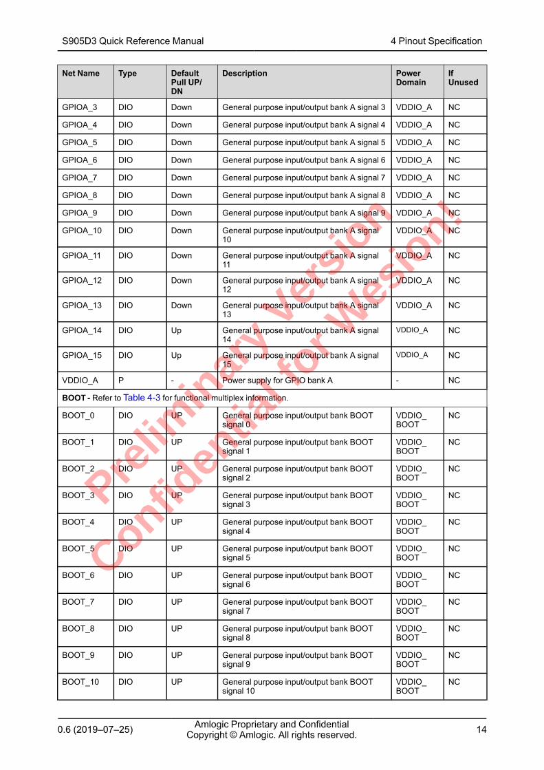
S905D3 Quick Reference Manual 4 Pinout Specification
Prelim
inar
y Ver
sion
Confiden
tial f
or Wes
ion!
0.6 (2019–07–25) Amlogic Proprietary and ConfidentialCopyright © Amlogic. All rights reserved. 14
Net Name Type DefaultPull UP/DN
Description PowerDomain
IfUnused
GPIOA_3 DIO Down General purpose input/output bank A signal 3 VDDIO_A NC
GPIOA_4 DIO Down General purpose input/output bank A signal 4 VDDIO_A NC
GPIOA_5 DIO Down General purpose input/output bank A signal 5 VDDIO_A NC
GPIOA_6 DIO Down General purpose input/output bank A signal 6 VDDIO_A NC
GPIOA_7 DIO Down General purpose input/output bank A signal 7 VDDIO_A NC
GPIOA_8 DIO Down General purpose input/output bank A signal 8 VDDIO_A NC
GPIOA_9 DIO Down General purpose input/output bank A signal 9 VDDIO_A NC
GPIOA_10 DIO Down General purpose input/output bank A signal10
VDDIO_A NC
GPIOA_11 DIO Down General purpose input/output bank A signal11
VDDIO_A NC
GPIOA_12 DIO Down General purpose input/output bank A signal12
VDDIO_A NC
GPIOA_13 DIO Down General purpose input/output bank A signal13
VDDIO_A NC
GPIOA_14 DIO Up General purpose input/output bank A signal14
VDDIO_A NC
GPIOA_15 DIO Up General purpose input/output bank A signal15
VDDIO_A NC
VDDIO_A P - Power supply for GPIO bank A - NC
BOOT - Refer to Table 4-3 for functional multiplex information.
BOOT_0 DIO UP General purpose input/output bank BOOTsignal 0
VDDIO_BOOT
NC
BOOT_1 DIO UP General purpose input/output bank BOOTsignal 1
VDDIO_BOOT
NC
BOOT_2 DIO UP General purpose input/output bank BOOTsignal 2
VDDIO_BOOT
NC
BOOT_3 DIO UP General purpose input/output bank BOOTsignal 3
VDDIO_BOOT
NC
BOOT_4 DIO UP General purpose input/output bank BOOTsignal 4
VDDIO_BOOT
NC
BOOT_5 DIO UP General purpose input/output bank BOOTsignal 5
VDDIO_BOOT
NC
BOOT_6 DIO UP General purpose input/output bank BOOTsignal 6
VDDIO_BOOT
NC
BOOT_7 DIO UP General purpose input/output bank BOOTsignal 7
VDDIO_BOOT
NC
BOOT_8 DIO UP General purpose input/output bank BOOTsignal 8
VDDIO_BOOT
NC
BOOT_9 DIO UP General purpose input/output bank BOOTsignal 9
VDDIO_BOOT
NC
BOOT_10 DIO UP General purpose input/output bank BOOTsignal 10
VDDIO_BOOT
NC
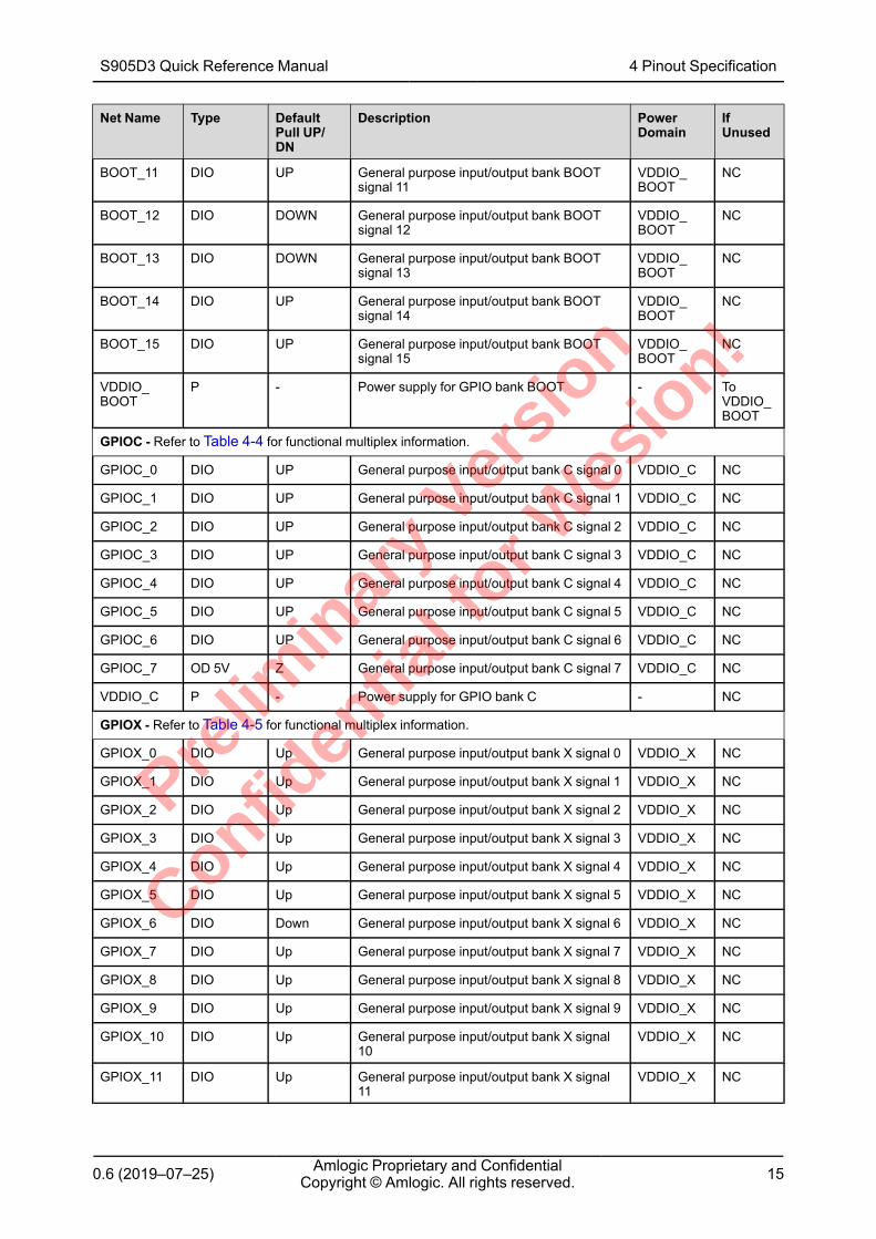
S905D3 Quick Reference Manual 4 Pinout Specification
Prelim
inar
y Ver
sion
Confiden
tial f
or Wes
ion!
0.6 (2019–07–25) Amlogic Proprietary and ConfidentialCopyright © Amlogic. All rights reserved. 15
Net Name Type DefaultPull UP/DN
Description PowerDomain
IfUnused
BOOT_11 DIO UP General purpose input/output bank BOOTsignal 11
VDDIO_BOOT
NC
BOOT_12 DIO DOWN General purpose input/output bank BOOTsignal 12
VDDIO_BOOT
NC
BOOT_13 DIO DOWN General purpose input/output bank BOOTsignal 13
VDDIO_BOOT
NC
BOOT_14 DIO UP General purpose input/output bank BOOTsignal 14
VDDIO_BOOT
NC
BOOT_15 DIO UP General purpose input/output bank BOOTsignal 15
VDDIO_BOOT
NC
VDDIO_BOOT
P - Power supply for GPIO bank BOOT - ToVDDIO_BOOT
GPIOC - Refer to Table 4-4 for functional multiplex information.
GPIOC_0 DIO UP General purpose input/output bank C signal 0 VDDIO_C NC
GPIOC_1 DIO UP General purpose input/output bank C signal 1 VDDIO_C NC
GPIOC_2 DIO UP General purpose input/output bank C signal 2 VDDIO_C NC
GPIOC_3 DIO UP General purpose input/output bank C signal 3 VDDIO_C NC
GPIOC_4 DIO UP General purpose input/output bank C signal 4 VDDIO_C NC
GPIOC_5 DIO UP General purpose input/output bank C signal 5 VDDIO_C NC
GPIOC_6 DIO UP General purpose input/output bank C signal 6 VDDIO_C NC
GPIOC_7 OD 5V Z General purpose input/output bank C signal 7 VDDIO_C NC
VDDIO_C P - Power supply for GPIO bank C - NC
GPIOX - Refer to Table 4-5 for functional multiplex information.
GPIOX_0 DIO Up General purpose input/output bank X signal 0 VDDIO_X NC
GPIOX_1 DIO Up General purpose input/output bank X signal 1 VDDIO_X NC
GPIOX_2 DIO Up General purpose input/output bank X signal 2 VDDIO_X NC
GPIOX_3 DIO Up General purpose input/output bank X signal 3 VDDIO_X NC
GPIOX_4 DIO Up General purpose input/output bank X signal 4 VDDIO_X NC
GPIOX_5 DIO Up General purpose input/output bank X signal 5 VDDIO_X NC
GPIOX_6 DIO Down General purpose input/output bank X signal 6 VDDIO_X NC
GPIOX_7 DIO Up General purpose input/output bank X signal 7 VDDIO_X NC
GPIOX_8 DIO Up General purpose input/output bank X signal 8 VDDIO_X NC
GPIOX_9 DIO Up General purpose input/output bank X signal 9 VDDIO_X NC
GPIOX_10 DIO Up General purpose input/output bank X signal10
VDDIO_X NC
GPIOX_11 DIO Up General purpose input/output bank X signal11
VDDIO_X NC
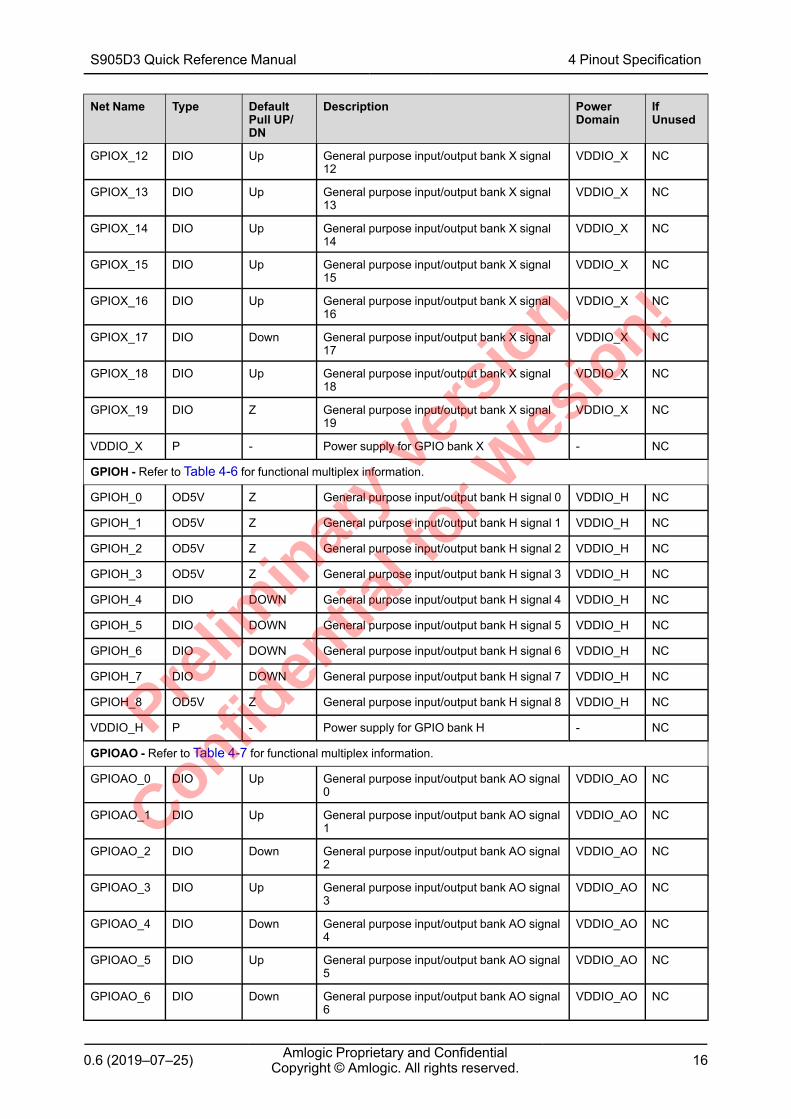
S905D3 Quick Reference Manual 4 Pinout Specification
Prelim
inar
y Ver
sion
Confiden
tial f
or Wes
ion!
0.6 (2019–07–25) Amlogic Proprietary and ConfidentialCopyright © Amlogic. All rights reserved. 16
Net Name Type DefaultPull UP/DN
Description PowerDomain
IfUnused
GPIOX_12 DIO Up General purpose input/output bank X signal12
VDDIO_X NC
GPIOX_13 DIO Up General purpose input/output bank X signal13
VDDIO_X NC
GPIOX_14 DIO Up General purpose input/output bank X signal14
VDDIO_X NC
GPIOX_15 DIO Up General purpose input/output bank X signal15
VDDIO_X NC
GPIOX_16 DIO Up General purpose input/output bank X signal16
VDDIO_X NC
GPIOX_17 DIO Down General purpose input/output bank X signal17
VDDIO_X NC
GPIOX_18 DIO Up General purpose input/output bank X signal18
VDDIO_X NC
GPIOX_19 DIO Z General purpose input/output bank X signal19
VDDIO_X NC
VDDIO_X P - Power supply for GPIO bank X - NC
GPIOH - Refer to Table 4-6 for functional multiplex information.
GPIOH_0 OD5V Z General purpose input/output bank H signal 0 VDDIO_H NC
GPIOH_1 OD5V Z General purpose input/output bank H signal 1 VDDIO_H NC
GPIOH_2 OD5V Z General purpose input/output bank H signal 2 VDDIO_H NC
GPIOH_3 OD5V Z General purpose input/output bank H signal 3 VDDIO_H NC
GPIOH_4 DIO DOWN General purpose input/output bank H signal 4 VDDIO_H NC
GPIOH_5 DIO DOWN General purpose input/output bank H signal 5 VDDIO_H NC
GPIOH_6 DIO DOWN General purpose input/output bank H signal 6 VDDIO_H NC
GPIOH_7 DIO DOWN General purpose input/output bank H signal 7 VDDIO_H NC
GPIOH_8 OD5V Z General purpose input/output bank H signal 8 VDDIO_H NC
VDDIO_H P - Power supply for GPIO bank H - NC
GPIOAO - Refer to Table 4-7 for functional multiplex information.
GPIOAO_0 DIO Up General purpose input/output bank AO signal0
VDDIO_AO NC
GPIOAO_1 DIO Up General purpose input/output bank AO signal1
VDDIO_AO NC
GPIOAO_2 DIO Down General purpose input/output bank AO signal2
VDDIO_AO NC
GPIOAO_3 DIO Up General purpose input/output bank AO signal3
VDDIO_AO NC
GPIOAO_4 DIO Down General purpose input/output bank AO signal4
VDDIO_AO NC
GPIOAO_5 DIO Up General purpose input/output bank AO signal5
VDDIO_AO NC
GPIOAO_6 DIO Down General purpose input/output bank AO signal6
VDDIO_AO NC
S905D3 Quick Reference Manual 4 Pinout Specification
Prelim
inar
y Ver
sion
Confiden
tial f
or Wes
ion!
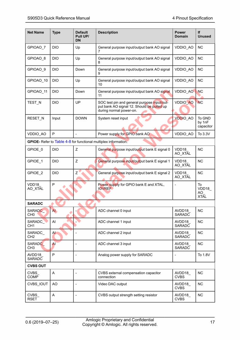
0.6 (2019–07–25) Amlogic Proprietary and ConfidentialCopyright © Amlogic. All rights reserved. 17
Net Name Type DefaultPull UP/DN
Description PowerDomain
IfUnused
GPIOAO_7 DIO Up General purpose input/output bank AO signal7
VDDIO_AO NC
GPIOAO_8 DIO Up General purpose input/output bank AO signal8
VDDIO_AO NC
GPIOAO_9 DIO Down General purpose input/output bank AO signal9
VDDIO_AO NC
GPIOAO_10 DIO Up General purpose input/output bank AO signal10
VDDIO_AO NC
GPIOAO_11 DIO Down General purpose input/output bank AO signal11
VDDIO_AO NC
TEST_N DIO UP SOC test pin and general purpose input/out-put bank AO signal 12. Should be pulled upduring normal power-on.
VDDIO_AO NC
RESET_N Input DOWN System reset input VDDIO_AO To GNDby 1nFcapacitor
VDDIO_AO P - Power supply for GPIO bank AO VDDIO_AO To 3.3V
GPIOE- Refer to Table 4-8 for functional multiplex information.
GPIOE_0 DIO Z General purpose input/output bank E signal 0 VDD18_AO_XTAL
NC
GPIOE_1 DIO Z General purpose input/output bank E signal 1 VDD18_AO_XTAL
NC
GPIOE_2 DIO Z General purpose input/output bank E signal 2 VDD18_AO_XTAL
NC
VDD18_AO_XTAL
P - Power supply for GPIO bank E and XTAL,IOVREF
- ToVDD18_AO_XTAL
SARADC
SARADC_CH0
AI - ADC channel 0 input AVDD18_SARADC
NC
SARADC_CH1
AI - ADC channel 1 input AVDD18_SARADC
NC
SARADC_CH2
AI - ADC channel 2 input AVDD18_SARADC
NC
SARADC_CH3
AI - ADC channel 3 input AVDD18_SARADC
NC
AVDD18_SARADC
P - Analog power supply for SARADC - To 1.8V
CVBS OUT
CVBS_COMP
A - CVBS external compensation capacitorconnection
AVDD18_CVBS
NC
CVBS_IOUT AO - Video DAC output AVDD18_CVBS
NC
CVBS_RSET
A - CVBS output strength setting resistor AVDD18_CVBS
NC
S905D3 Quick Reference Manual 4 Pinout Specification
Prelim
inar
y Ver
sion
Confiden
tial f
or Wes
ion!
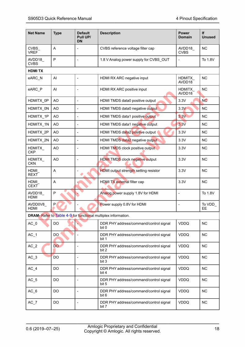
0.6 (2019–07–25) Amlogic Proprietary and ConfidentialCopyright © Amlogic. All rights reserved. 18
Net Name Type DefaultPull UP/DN
Description PowerDomain
IfUnused
CVBS_VREF
A - CVBS reference voltage filter cap AVDD18_CVBS
NC
AVDD18_CVBS
P - 1.8 VAnalog power supply for CVBS_OUT - To 1.8V
HDMI TX
eARC_N AI - HDMI RX ARC negative input HDMITX_AVDD18
NC
eARC_P AI - HDMI RX ARC positive input HDMITX_AVDD18
NC
HDMITX_0P AO - HDMI TMDS data0 positive output 3.3V NC
HDMITX_0N AO - HDMI TMDS data0 negative output 3.3V NC
HDMITX_1P AO - HDMI TMDS data1 positive output 3.3V NC
HDMITX_1N AO - HDMI TMDS data1 negative output 3.3V NC
HDMITX_2P AO - HDMI TMDS data2 positive output 3.3V NC
HDMITX_2N AO - HDMI TMDS data2 negative output 3.3V NC
HDMITX_CKP
AO - HDMI TMDS clock positive output 3.3V NC
HDMITX_CKN
AO - HDMI TMDS clock negative output 3.3V NC
HDMI_REXT
A - HDMI output strength setting resistor 3.3V NC
HDMI_CEXT
A - HDMI TX external filter cap 3.3V NC
AVDD18_HDMI
P - Analog power supply 1.8V for HDMI - To 1.8V
AVDD0V8_HDMI
P - Power supply 0.8V for HDMI - To VDD_EE
DRAM- Refer to Table 4-9 for functional multiplex information.
AC_0 DO - DDR PHYaddress/command/control signalbit 0
VDDQ NC
AC_1 DO - DDR PHYaddress/command/control signalbit 1
VDDQ NC
AC_2 DO - DDR PHYaddress/command/control signalbit 2
VDDQ NC
AC_3 DO - DDR PHYaddress/command/control signalbit 3
VDDQ NC
AC_4 DO - DDR PHYaddress/command/control signalbit 4
VDDQ NC
AC_5 DO - DDR PHYaddress/command/control signalbit 5
VDDQ NC
AC_6 DO - DDR PHYaddress/command/control signalbit 6
VDDQ NC
AC_7 DO - DDR PHYaddress/command/control signalbit 7
VDDQ NC
S905D3 Quick Reference Manual 4 Pinout Specification
Prelim
inar
y Ver
sion
Confiden
tial f
or Wes
ion!
0.6 (2019–07–25) Amlogic Proprietary and ConfidentialCopyright © Amlogic. All rights reserved. 19
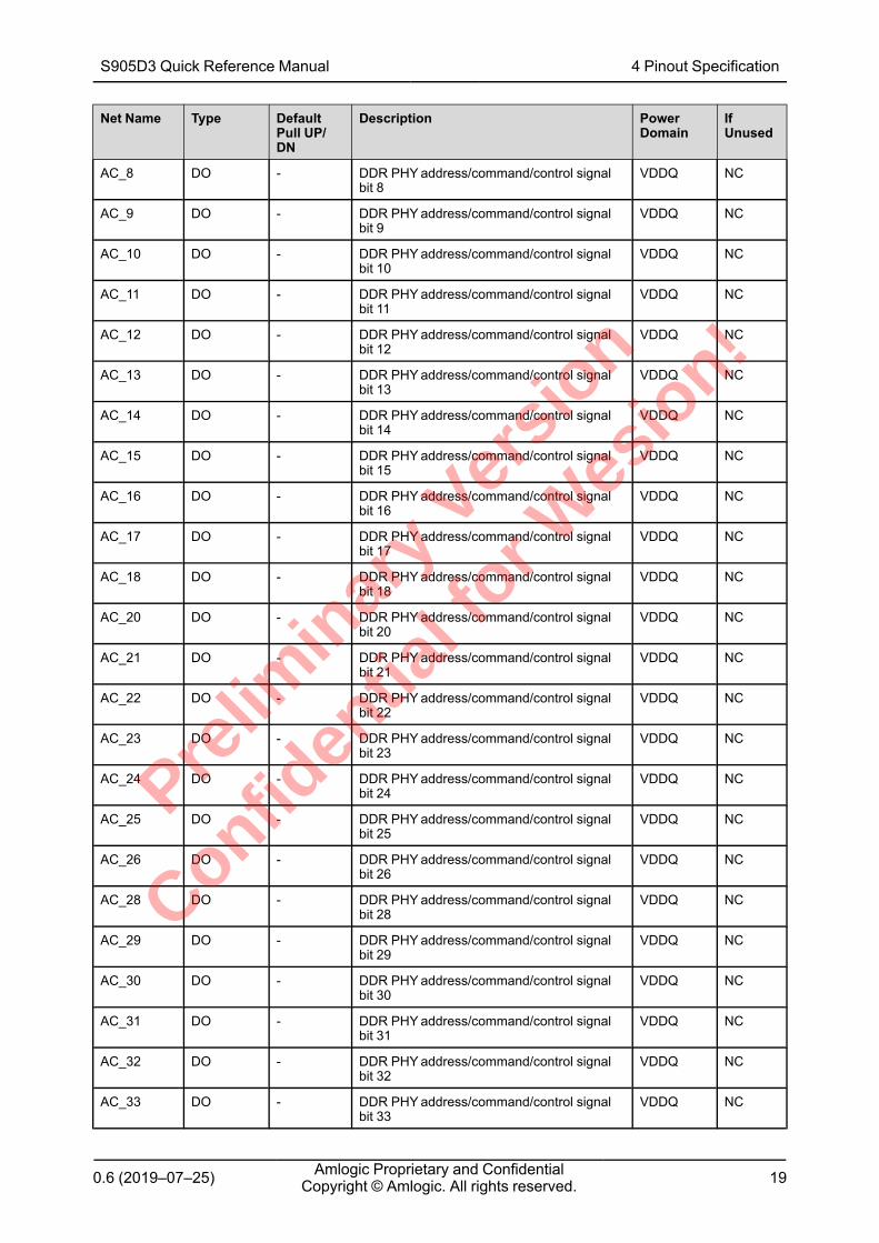
Net Name Type DefaultPull UP/DN
Description PowerDomain
IfUnused
AC_8 DO - DDR PHYaddress/command/control signalbit 8
VDDQ NC
AC_9 DO - DDR PHYaddress/command/control signalbit 9
VDDQ NC
AC_10 DO - DDR PHYaddress/command/control signalbit 10
VDDQ NC
AC_11 DO - DDR PHYaddress/command/control signalbit 11
VDDQ NC
AC_12 DO - DDR PHYaddress/command/control signalbit 12
VDDQ NC
AC_13 DO - DDR PHYaddress/command/control signalbit 13
VDDQ NC
AC_14 DO - DDR PHYaddress/command/control signalbit 14
VDDQ NC
AC_15 DO - DDR PHYaddress/command/control signalbit 15
VDDQ NC
AC_16 DO - DDR PHYaddress/command/control signalbit 16
VDDQ NC
AC_17 DO - DDR PHYaddress/command/control signalbit 17
VDDQ NC
AC_18 DO - DDR PHYaddress/command/control signalbit 18
VDDQ NC
AC_20 DO - DDR PHYaddress/command/control signalbit 20
VDDQ NC
AC_21 DO - DDR PHYaddress/command/control signalbit 21
VDDQ NC
AC_22 DO - DDR PHYaddress/command/control signalbit 22
VDDQ NC
AC_23 DO - DDR PHYaddress/command/control signalbit 23
VDDQ NC
AC_24 DO - DDR PHYaddress/command/control signalbit 24
VDDQ NC
AC_25 DO - DDR PHYaddress/command/control signalbit 25
VDDQ NC
AC_26 DO - DDR PHYaddress/command/control signalbit 26
VDDQ NC
AC_28 DO - DDR PHYaddress/command/control signalbit 28
VDDQ NC
AC_29 DO - DDR PHYaddress/command/control signalbit 29
VDDQ NC
AC_30 DO - DDR PHYaddress/command/control signalbit 30
VDDQ NC
AC_31 DO - DDR PHYaddress/command/control signalbit 31
VDDQ NC
AC_32 DO - DDR PHYaddress/command/control signalbit 32
VDDQ NC
AC_33 DO - DDR PHYaddress/command/control signalbit 33
VDDQ NC
S905D3 Quick Reference Manual 4 Pinout Specification
Prelim
inar
y Ver
sion
Confiden
tial f
or Wes
ion!
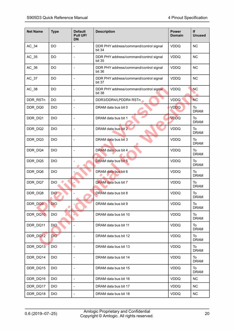
0.6 (2019–07–25) Amlogic Proprietary and ConfidentialCopyright © Amlogic. All rights reserved. 20
Net Name Type DefaultPull UP/DN
Description PowerDomain
IfUnused
AC_34 DO - DDR PHYaddress/command/control signalbit 34
VDDQ NC
AC_35 DO - DDR PHYaddress/command/control signalbit 35
VDDQ NC
AC_36 DO - DDR PHYaddress/command/control signalbit 36
VDDQ NC
AC_37 DO - DDR PHYaddress/command/control signalbit 37
VDDQ NC
AC_38 DO - DDR PHYaddress/command/control signalbit 38
VDDQ NC
DDR_RSTn DO - DDR3/DDR4/LPDDR4 RSTn VDDQ NC
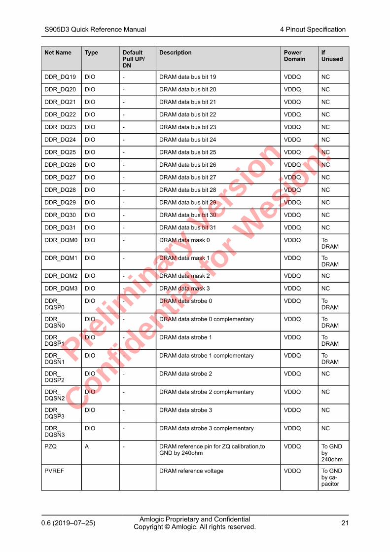
DDR_DQ0 DIO - DRAM data bus bit 0 VDDQ ToDRAM
DDR_DQ1 DIO - DRAM data bus bit 1 VDDQ ToDRAM
DDR_DQ2 DIO - DRAM data bus bit 2 VDDQ ToDRAM
DDR_DQ3 DIO - DRAM data bus bit 3 VDDQ ToDRAM
DDR_DQ4 DIO - DRAM data bus bit 4 VDDQ ToDRAM
DDR_DQ5 DIO - DRAM data bus bit 5 VDDQ ToDRAM
DDR_DQ6 DIO - DRAM data bus bit 6 VDDQ ToDRAM
DDR_DQ7 DIO - DRAM data bus bit 7 VDDQ ToDRAM
DDR_DQ8 DIO - DRAM data bus bit 8 VDDQ ToDRAM
DDR_DQ9 DIO - DRAM data bus bit 9 VDDQ ToDRAM
DDR_DQ10 DIO - DRAM data bus bit 10 VDDQ ToDRAM
DDR_DQ11 DIO - DRAM data bus bit 11 VDDQ ToDRAM
DDR_DQ12 DIO - DRAM data bus bit 12 VDDQ ToDRAM
DDR_DQ13 DIO - DRAM data bus bit 13 VDDQ ToDRAM
DDR_DQ14 DIO - DRAM data bus bit 14 VDDQ ToDRAM
DDR_DQ15 DIO - DRAM data bus bit 15 VDDQ ToDRAM
DDR_DQ16 DIO - DRAM data bus bit 16 VDDQ NC
DDR_DQ17 DIO - DRAM data bus bit 17 VDDQ NC
DDR_DQ18 DIO - DRAM data bus bit 18 VDDQ NC
S905D3 Quick Reference Manual 4 Pinout Specification
Prelim
inar
y Ver
sion
Confiden
tial f
or Wes
ion!
0.6 (2019–07–25) Amlogic Proprietary and ConfidentialCopyright © Amlogic. All rights reserved. 21
Net Name Type DefaultPull UP/DN
Description PowerDomain
IfUnused
DDR_DQ19 DIO - DRAM data bus bit 19 VDDQ NC
DDR_DQ20 DIO - DRAM data bus bit 20 VDDQ NC
DDR_DQ21 DIO - DRAM data bus bit 21 VDDQ NC
DDR_DQ22 DIO - DRAM data bus bit 22 VDDQ NC
DDR_DQ23 DIO - DRAM data bus bit 23 VDDQ NC
DDR_DQ24 DIO - DRAM data bus bit 24 VDDQ NC
DDR_DQ25 DIO - DRAM data bus bit 25 VDDQ NC
DDR_DQ26 DIO - DRAM data bus bit 26 VDDQ NC
DDR_DQ27 DIO - DRAM data bus bit 27 VDDQ NC
DDR_DQ28 DIO - DRAM data bus bit 28 VDDQ NC
DDR_DQ29 DIO - DRAM data bus bit 29 VDDQ NC
DDR_DQ30 DIO - DRAM data bus bit 30 VDDQ NC
DDR_DQ31 DIO - DRAM data bus bit 31 VDDQ NC
DDR_DQM0 DIO - DRAM data mask 0 VDDQ ToDRAM
DDR_DQM1 DIO - DRAM data mask 1 VDDQ ToDRAM
DDR_DQM2 DIO - DRAM data mask 2 VDDQ NC
DDR_DQM3 DIO - DRAM data mask 3 VDDQ NC
DDR_DQSP0
DIO - DRAM data strobe 0 VDDQ ToDRAM
DDR_DQSN0
DIO - DRAM data strobe 0 complementary VDDQ ToDRAM
DDR_DQSP1
DIO - DRAM data strobe 1 VDDQ ToDRAM
DDR_DQSN1
DIO - DRAM data strobe 1 complementary VDDQ ToDRAM
DDR_DQSP2
DIO - DRAM data strobe 2 VDDQ NC
DDR_DQSN2
DIO - DRAM data strobe 2 complementary VDDQ NC
DDR_DQSP3
DIO - DRAM data strobe 3 VDDQ NC
DDR_DQSN3
DIO - DRAM data strobe 3 complementary VDDQ NC
PZQ A - DRAM reference pin for ZQ calibration,toGND by 240ohm
VDDQ To GNDby240ohm
PVREF DRAM reference voltage VDDQ To GNDby ca-pacitor
S905D3 Quick Reference Manual 4 Pinout Specification
Prelim
inar
y Ver
sion
Confiden
tial f
or Wes
ion!
0.6 (2019–07–25) Amlogic Proprietary and ConfidentialCopyright © Amlogic. All rights reserved. 22
Net Name Type DefaultPull UP/DN
Description PowerDomain
IfUnused
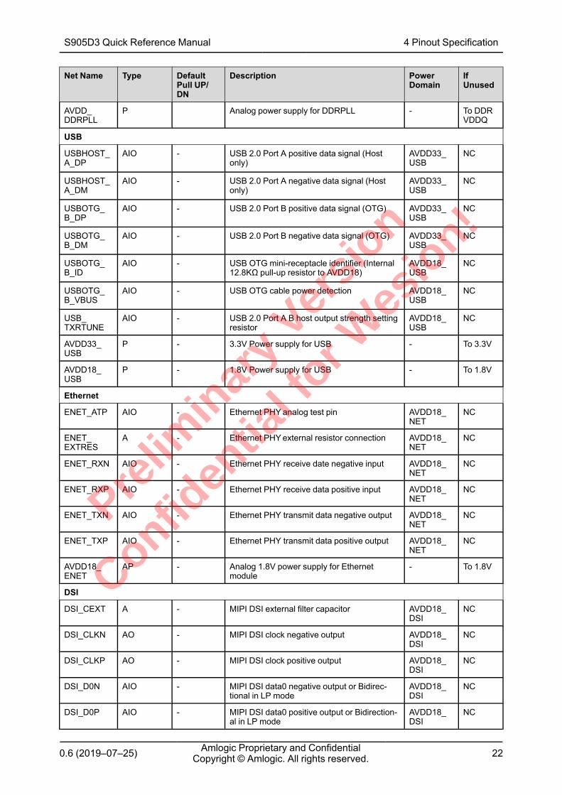
AVDD_DDRPLL
P Analog power supply for DDRPLL - To DDRVDDQ
USB
USBHOST_A_DP
AIO - USB 2.0 Port A positive data signal (Hostonly)
AVDD33_USB
NC
USBHOST_A_DM
AIO - USB 2.0 Port A negative data signal (Hostonly)
AVDD33_USB
NC
USBOTG_B_DP
AIO - USB 2.0 Port B positive data signal (OTG) AVDD33_USB
NC
USBOTG_B_DM
AIO - USB 2.0 Port B negative data signal (OTG) AVDD33_USB
NC
USBOTG_B_ID
AIO - USB OTG mini-receptacle identifier (Internal12.8KΩ pull-up resistor to AVDD18)
AVDD18_USB
NC
USBOTG_B_VBUS
AIO - USB OTG cable power detection AVDD18_USB
NC
USB_TXRTUNE
AIO - USB 2.0 Port A B host output strength settingresistor
AVDD18_USB
NC
AVDD33_USB
P - 3.3V Power supply for USB - To 3.3V
AVDD18_USB
P - 1.8V Power supply for USB - To 1.8V
Ethernet
ENET_ATP AIO - Ethernet PHY analog test pin AVDD18_NET
NC
ENET_EXTRES
A - Ethernet PHYexternal resistor connection AVDD18_NET
NC
ENET_RXN AIO - Ethernet PHY receive date negative input AVDD18_NET
NC
ENET_RXP AIO - Ethernet PHY receive data positive input AVDD18_NET
NC
ENET_TXN AIO - Ethernet PHY transmit data negative output AVDD18_NET
NC
ENET_TXP AIO - Ethernet PHY transmit data positive output AVDD18_NET
NC
AVDD18_ENET
AP - Analog 1.8V power supply for Ethernetmodule
- To 1.8V
DSI
DSI_CEXT A - MIPI DSI external filter capacitor AVDD18_DSI
NC
DSI_CLKN AO - MIPI DSI clock negative output AVDD18_DSI
NC
DSI_CLKP AO - MIPI DSI clock positive output AVDD18_DSI
NC
DSI_D0N AIO - MIPI DSI data0 negative output or Bidirec-tional in LP mode
AVDD18_DSI
NC
DSI_D0P AIO - MIPI DSI data0 positive output or Bidirection-al in LP mode
AVDD18_DSI
NC
S905D3 Quick Reference Manual 4 Pinout Specification
Prelim
inar
y Ver
sion
Confiden
tial f
or Wes
ion!
0.6 (2019–07–25) Amlogic Proprietary and ConfidentialCopyright © Amlogic. All rights reserved. 23
Net Name Type DefaultPull UP/DN
Description PowerDomain
IfUnused
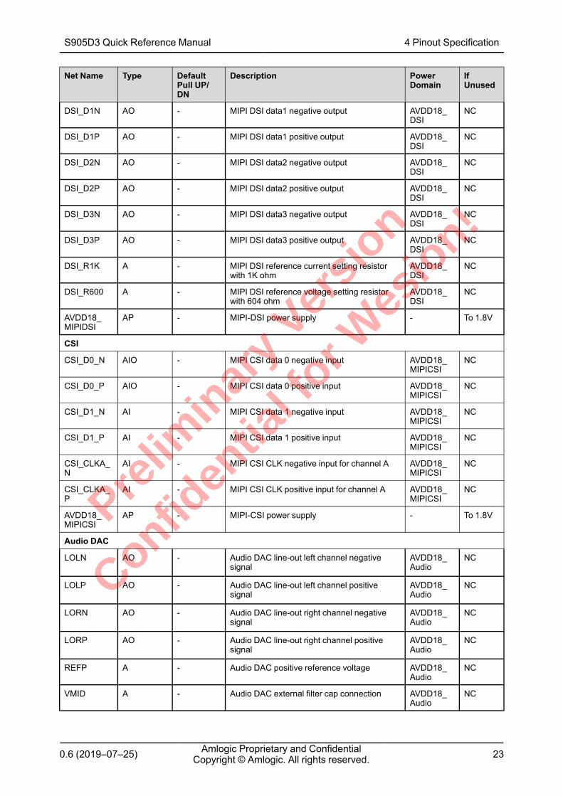
DSI_D1N AO - MIPI DSI data1 negative output AVDD18_DSI
NC
DSI_D1P AO - MIPI DSI data1 positive output AVDD18_DSI
NC
DSI_D2N AO - MIPI DSI data2 negative output AVDD18_DSI
NC
DSI_D2P AO - MIPI DSI data2 positive output AVDD18_DSI
NC
DSI_D3N AO - MIPI DSI data3 negative output AVDD18_DSI
NC
DSI_D3P AO - MIPI DSI data3 positive output AVDD18_DSI
NC
DSI_R1K A - MIPI DSI reference current setting resistorwith 1K ohm
AVDD18_DSI
NC
DSI_R600 A - MIPI DSI reference voltage setting resistorwith 604 ohm
AVDD18_DSI
NC
AVDD18_MIPIDSI
AP - MIPI-DSI power supply - To 1.8V
CSI
CSI_D0_N AIO - MIPI CSI data 0 negative input AVDD18_MIPICSI
NC
CSI_D0_P AIO - MIPI CSI data 0 positive input AVDD18_MIPICSI
NC
CSI_D1_N AI - MIPI CSI data 1 negative input AVDD18_MIPICSI
NC
CSI_D1_P AI - MIPI CSI data 1 positive input AVDD18_MIPICSI
NC
CSI_CLKA_N
AI - MIPI CSI CLK negative input for channel A AVDD18_MIPICSI
NC
CSI_CLKA_P
AI - MIPI CSI CLK positive input for channel A AVDD18_MIPICSI
NC
AVDD18_MIPICSI
AP - MIPI-CSI power supply - To 1.8V
Audio DAC
LOLN AO - Audio DAC line-out left channel negativesignal
AVDD18_Audio
NC
LOLP AO - Audio DAC line-out left channel positivesignal
AVDD18_Audio
NC
LORN AO - Audio DAC line-out right channel negativesignal
AVDD18_Audio
NC
LORP AO - Audio DAC line-out right channel positivesignal
AVDD18_Audio
NC
REFP A - Audio DAC positive reference voltage AVDD18_Audio
NC
VMID A - Audio DAC external filter cap connection AVDD18_Audio
NC
S905D3 Quick Reference Manual 4 Pinout Specification
Prelim
inar
y Ver
sion
Confiden
tial f
or Wes
ion!
0.6 (2019–07–25) Amlogic Proprietary and ConfidentialCopyright © Amlogic. All rights reserved. 24
Net Name Type DefaultPull UP/DN
Description PowerDomain
IfUnused
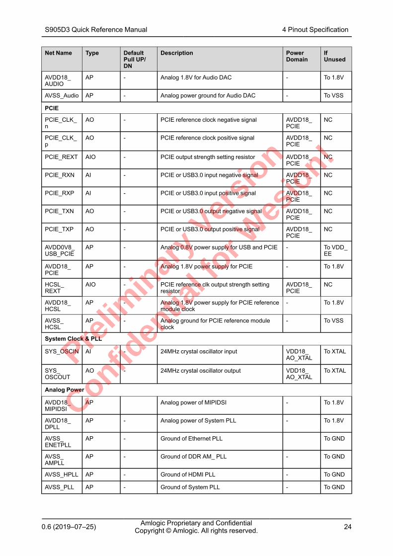
AVDD18_AUDIO
AP - Analog 1.8V for Audio DAC - To 1.8V
AVSS_Audio AP - Analog power ground for Audio DAC - To VSS
PCIE
PCIE_CLK_n
AO - PCIE reference clock negative signal AVDD18_PCIE
NC
PCIE_CLK_p
AO - PCIE reference clock positive signal AVDD18_PCIE
NC
PCIE_REXT AIO - PCIE output strength setting resistor AVDD18_PCIE
NC
PCIE_RXN AI - PCIE or USB3.0 input negative signal AVDD18_PCIE
NC
PCIE_RXP AI - PCIE or USB3.0 input positive signal AVDD18_PCIE
NC
PCIE_TXN AO - PCIE or USB3.0 output negative signal AVDD18_PCIE
NC
PCIE_TXP AO - PCIE or USB3.0 output positive signal AVDD18_PCIE
NC
AVDD0V8_USB_PCIE
AP - Analog 0.8V power supply for USB and PCIE - To VDD_EE
AVDD18_PCIE
AP - Analog 1.8V power supply for PCIE - To 1.8V
HCSL_REXT
AIO - PCIE reference clk output strength settingresistor
AVDD18_PCIE
NC
AVDD18_HCSL
AP - Analog 1.8V power supply for PCIE referencemodule clock
- To 1.8V
AVSS_HCSL
AP - Analog ground for PCIE reference moduleclock
- To VSS
System Clock & PLL
SYS_OSCIN AI - 24MHz crystal oscillator input VDD18_AO_XTAL
To XTAL
SYS_OSCOUT
AO - 24MHz crystal oscillator output VDD18_AO_XTAL
To XTAL
Analog Power
AVDD18_MIPIDSI
AP Analog power of MIPIDSI - To 1.8V
AVDD18_DPLL
AP - Analog power of System PLL - To 1.8V
AVSS_ENETPLL
AP - Ground of Ethernet PLL To GND
AVSS_AMPLL
AP - Ground of DDR AM_ PLL - To GND
AVSS_HPLL AP - Ground of HDMI PLL - To GND
AVSS_PLL AP - Ground of System PLL - To GND
S905D3 Quick Reference Manual 4 Pinout Specification
Prelim
inar
y Ver
sion
Confiden
tial f
or Wes
ion!
0.6 (2019–07–25) Amlogic Proprietary and ConfidentialCopyright © Amlogic. All rights reserved. 25
Net Name Type DefaultPull UP/DN
Description PowerDomain
IfUnused
AVSS_CVBS
AP Ground of CVBS digital-analog converter - To GND
Digital Power
VDDCPU P - Power supply for CPU (Cortex A55) - ToVDDCP-U
VDDQ P - DDR IO Power supply for DDR PHY - ToVDDQ
VDD_DDR P - Core Power supply for DDR PHY - To VDD_EE
VDD_EE P - Power supply for GPU and core logic - To VDD_EE
VDD18_AO_XTAL
P - 1.8V Power supply for Always On Domain - ToVDD18_AO_XTAL
Digital Ground
DVSS P - Digital power ground - To GND
Abbreviations:●● DI = Digital input pin●● DO = Digital output pin●● DIO = Digital input/output pin●● OD 5V = 5V input tolerant open drain (OD) output pin, need external pull up●● A = Analog setting or filtering pin●● AI = Analog input pin●● AO = Analog output pin●● AIO = Analog input/output pin●● P = Power pin●● AP = Analog power pin●● NC = No connection●● UP = Pull-Up●● DOWN = Pull-down●● Z = High-Z
4.4 Pin Multiplexing TablesMultiple usage pins are used to conserve pin consumption for different features. The devices can beused in many different applications but each application will not utilize all the on chip features. As aresult, some of the features share the same pin. Most of the multiple usage pins can be used as aGPIO pin as well.
S905D3 Quick Reference Manual 4 Pinout Specification
Prelim
inar
y Ver
sion
Confiden
tial f
or Wes
ion!
0.6 (2019–07–25) Amlogic Proprietary and ConfidentialCopyright © Amlogic. All rights reserved. 26
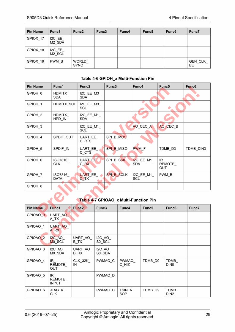
Table 4-1 GPIOZ_x Multi-Function Pin
Pin Name Func1 Func2 Func3 Func4 Func5 Func6 Func7
GPIOZ_0 ETH_MDIO ISO7816_CLK
I2C_EE_M0_SDA
PWM_B I2C_EE_M1_SDA
GPIOZ_1 ETH_MDC ISO7816_DATA
I2C_EE_M0_SCL
PWM_C I2C_EE_M1_SCL
GPIOZ_2 ETH_RGMII_RX_CLK
PWM_D TSIN_B_VALID
TDMC_D0 SDCARD_D0
TDMC_DIN0
PDM_DIN0
GPIOZ_3 ETH_RX_DV
TSIN_B_SOP
TDMC_D1 SDCARD_D1
TDMC_DIN1
PDM_DIN1
GPIOZ_4 ETH_RXD0 TSIN_B_DIN0
TDMC_D2 SDCARD_D2
TDMC_DIN2
PDM_DIN2
GPIOZ_5 ETH_RXD1 TSIN_B_CLK
TDMC_D3 SDCARD_D3
TDMC_DIN3
PDM_DIN3
GPIOZ_6 ETH_RXD2_RGMII
TSIN_B_FAIL
TDMC_FS SDCARD_CLK
TDMC_SLV_FS
PDM_DCLK
GPIOZ_7 ETH_RXD3_RGMII
TSIN_B_DIN1
TDMC_SCLK
SDCARD_CMD
TDMC_SLV_SCLK
I2C_EE_M0_SDA
GPIOZ_8 ETH_RGMII_TX_CLK
TSIN_B_DIN2
MCLK_1 I2C_EE_M0_SCL
GPIOZ_9 ETH_TXEN
TSIN_B_DIN3
TDMC_D4
GPIOZ_10 ETH_TXD0 TSIN_B_DIN4
I2C_EE_M2_SDA
IR_REMOTE_OUT
GPIOZ_11 ETH_TXD1 TSIN_B_DIN5
I2C_EE_M2_SCL
GPIOZ_12 ETH_TXD2_RGMII
TSIN_B_DIN6
TDMC_D5 PWM_F
GPIOZ_13 ETH_TXD3_RGMII
CLK12_24 TSIN_B_DIN7
PWM_B GEN_CLK_EE
GPIOZ_14 ETH_LINK_LED
I2C_EE_M2_SDA
GPIOZ_15 ETH_ACT_LED
I2C_EE_M2_SCL
Table 4-2 GPIOA_x Multi-Function Pin
Pin Name Func1 Func2 Func3 Func4
GPIOA_0 MCLK_0 TDMB_D7
GPIOA_1 TDMB_SCLK TDMB_SLV_SCLK
GPIOA_2 TDMB_FS TDMB_SLV_FS
GPIOA_3 TDMB_D0 TDMB_DIN0
GPIOA_4 TDMB_D1 TDMB_DIN1 PWM_D
S905D3 Quick Reference Manual 4 Pinout Specification
Prelim
inar
y Ver
sion
Confiden
tial f
or Wes
ion!
0.6 (2019–07–25) Amlogic Proprietary and ConfidentialCopyright © Amlogic. All rights reserved. 27
Pin Name Func1 Func2 Func3 Func4
GPIOA_5 PDM_DIN3 TDMB_DIN2 TDMB_D2 TDMC_D5
GPIOA_6 PDM_DIN2 TDMB_DIN3 TDMB_D3 TDMC_D4
GPIOA_7 PDM_DCLK TDMC_D3 TDMC_DIN3 TDMB_D4
GPIOA_8 PDM_DIN0 TDMC_D2 TDMC_DIN2 TDMB_D5
GPIOA_9 PDM_DIN1 TDMC_D1 TDMC_DIN1 TDMB_D6
GPIOA_10 SPDIF_IN TDMC_D0 TDMC_DIN0
GPIOA_11 SPDIF_OUT MCLK_1 PWM_F
GPIOA_12 SPDIF_IN TDMC_SCLK TDMC_SLV_SCLK
GPIOA_13 SPDIF_OUT TDMC_FS TDMC_SLV_FS
GPIOA_14 WORLD_SYNC I2C_EE_M3_SDA TDMB_D7
GPIOA_15 IR_REMOTE_INPUT
I2C_EE_M3_SCL
Table 4-3 BOOT_x Multi-Function Pin
Pin Name Func1 Func2 Func3
BOOT_0 EMMC_D0
BOOT_1 EMMC_D1
BOOT_2 EMMC_D2
BOOT_3 EMMC_D3 NOR_HOLD
BOOT_4 EMMC_D4 NOR_D
BOOT_5 EMMC_D5 NOR_Q
BOOT_6 EMMC_D6 NOR_C
BOOT_7 EMMC_D7 NOR_WP
BOOT_8 EMMC_CLK NAND_WEN_CLK
BOOT_9 NAND_ALE
BOOT_10 EMMC_CMD NAND_CLE
BOOT_11 NAND_CE0
BOOT_12 NAND_REN_WR
BOOT_13 EMMC_NAND_DQS
BOOT_14 NAND_RB0 NOR_CS
BOOT_15 NAND_CE1
Table 4-4 GPIOC_x Multi-Function Pin
Pin Name Func1 Func2 Func3 Func4 Func5
GPIOC_0 SDCARD_D0 JTAG_B_TDO PDM_DIN0 SPI_A_MOSI
GPIOC_1 SDCARD_D1 JTAG_B_TDI PDM_DIN1 SPI_A_MISO
S905D3 Quick Reference Manual 4 Pinout Specification
Prelim
inar
y Ver
sion
Confiden
tial f
or Wes
ion!
0.6 (2019–07–25) Amlogic Proprietary and ConfidentialCopyright © Amlogic. All rights reserved. 28
Pin Name Func1 Func2 Func3 Func4 Func5
GPIOC_2 SDCARD_D2 UART_AO_A_RX
PDM_DIN2 SPI_A_SS0
GPIOC_3 SDCARD_D3 UART_AO_A_TX
PDM_DIN3 SPI_A_SCLK
GPIOC_4 SDCARD_CLK JTAG_B_CLK PDM_DCLK PWM_C
GPIOC_5 SDCARD_CMD JTAG_B_TMS I2C_EE_M0_SDA
ISO7816_CLK
GPIOC_6 I2C_EE_M0_SCL
ISO7816_DATA
GPIOC_7 PCIECK_REQN WORLD_SYNC
Table 4-5 GPIOX_x Multi-Function Pin
Pin Name Func1 Func2 Func3 Func4 Func5 Func6 Func7
GPIOX_0 SDIO_D0 PDM_DIN0 TSIN_A_DIN0
SDCARD_D0
GPIOX_1 SDIO_D1 PDM_DIN1 TSIN_A_SOP
SDCARD_D1
GPIOX_2 SDIO_D2 PDM_DIN2 TSIN_A_VALID
SDCARD_D2
GPIOX_3 SDIO_D3 PDM_DIN3 TSIN_A_CLK
PWM_D SDCARD_D3
GPIOX_4 SDIO_CLK PDM_DCLK
SDCARD_CLK
GPIOX_5 SDIO_CMD MCLK_1 PWM_C SDCARD_CMD
GPIOX_6 PWM_A UART_EE_B_TX
PWM_D
GPIOX_7 PWM_F UART_EE_B_RX
PWM_B
GPIOX_8 TDMA_D1 TDMA_DIN1
TSIN_B_SOP
SPI_A_MOSI
PWM_C ISO7816_CLK
GPIOX_9 TDMA_D0 TDMA_DIN0
TSIN_B_VALID
SPI_A_MISO
ISO7816_DATA
GPIOX_10 TDMA_FS TDMA_SLV_FS
TSIN_B_DIN0
SPI_A_SS0 I2C_EE_M1_SDA
GPIOX_11 TDMA_SCLK
TDMA_SLV_SCLK
TSIN_B_CLK
SPI_A_SCLK
I2C_EE_M1_SCL
GPIOX_12 UART_EE_A_TX
GPIOX_13 UART_EE_A_RX
GPIOX_14 UART_EE_A_CTS
GPIOX_15 UART_EE_A_RTS
GPIOX_16 PWM_E
S905D3 Quick Reference Manual 4 Pinout Specification
Prelim
inar
y Ver
sion
Confiden
tial f
or Wes
ion!
0.6 (2019–07–25) Amlogic Proprietary and ConfidentialCopyright © Amlogic. All rights reserved. 29
Pin Name Func1 Func2 Func3 Func4 Func5 Func6 Func7
GPIOX_17 I2C_EE_M2_SDA
GPIOX_18 I2C_EE_M2_SCL
GPIOX_19 PWM_B WORLD_SYNC
GEN_CLK_EE
Table 4-6 GPIOH_x Multi-Function Pin
Pin Name Func1 Func2 Func3 Func4 Func5 Func6
GPIOH_0 HDMITX_SDA
I2C_EE_M3_SDA
GPIOH_1 HDMITX_SCL I2C_EE_M3_SCL
GPIOH_2 HDMITX_HPD_IN
I2C_EE_M1_SDA
GPIOH_3 I2C_EE_M1_SCL
AO_CEC_A AO_CEC_B
GPIOH_4 SPDIF_OUT UART_EE_C_RTS
SPI_B_MOSI
GPIOH_5 SPDIF_IN UART_EE_C_CTS
SPI_B_MISO PWM_F TDMB_D3 TDMB_DIN3
GPIOH_6 ISO7816_CLK
UART_EE_C_RX
SPI_B_SS0 I2C_EE_M1_SDA
IR_REMOTE_OUT
GPIOH_7 ISO7816_DATA
UART_EE_C_TX
SPI_B_SCLK I2C_EE_M1_SCL
PWM_B
GPIOH_8
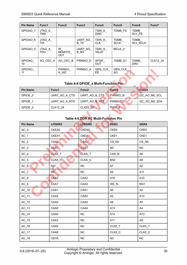
Table 4-7 GPIOAO_x Multi-Function Pin
Pin Name Func1 Func2 Func3 Func4 Func5 Func6 Func7
GPIOAO_0 UART_AO_A_TX
GPIOAO_1 UART_AO_A_RX
GPIOAO_2 I2C_AO_M0_SCL
UART_AO_B_TX
I2C_AO_S0_SCL
GPIOAO_3 I2C_AO_M0_SDA
UART_AO_B_RX
I2C_AO_S0_SDA
GPIOAO_4 IR_REMOTE_OUT
CLK_32K_IN
PWMAO_C PWMAO_C_HIZ
TDMB_D0 TDMB_DIN0
GPIOAO_5 IR_REMOTE_INPUT
PWMAO_D
GPIOAO_6 JTAG_A_CLK
PWMAO_C TSIN_A_SOP
TDMB_D2 TDMB_DIN2
S905D3 Quick Reference Manual 4 Pinout Specification
Prelim
inar
y Ver
sion
Confiden
tial f
or Wes
ion!
0.6 (2019–07–25) Amlogic Proprietary and ConfidentialCopyright © Amlogic. All rights reserved. 30
Pin Name Func1 Func2 Func3 Func4 Func5 Func6 Func7
GPIOAO_7 JTAG_A_TMS
TSIN_A_DIN0
TDMB_FS TDMB_SLV_FS
GPIOAO_8 JTAG_A_TDI
UART_AO_B_TX
TSIN_A_CLK
TDMB_SCLK
TDMB_SLV_SCLK
GPIOAO_9 JTAG_A_TDO
IR_REMOTE_OUT
UART_AO_B_RX
TSIN_A_VALID
MCLK_0
GPIOAO_10
AO_CEC_A AO_CEC_B PWMAO_D SPDIF_OUT
TDMB_D1 TDMB_DIN1
CLK12_24
GPIOAO_11
PWMAO_A_HIZ
PWMAO_A GEN_CLK_EE
GEN_CLK_AO
Table 4-8 GPIOE_x Multi-Function Pin
Pin Name Func1 Func2 Func3 Func4
GPIOE_0 UART_AO_A_CTS UART_AO_B_CTS PWMAO_B I2C_AO_M0_SCL
GPIOE_1 UART_AO_A_RTS UART_AO_B_RTS PWMAO_D I2C_AO_M0_SDA
GPIOE_2 CLK12_24 CLK25_EE PWM_A
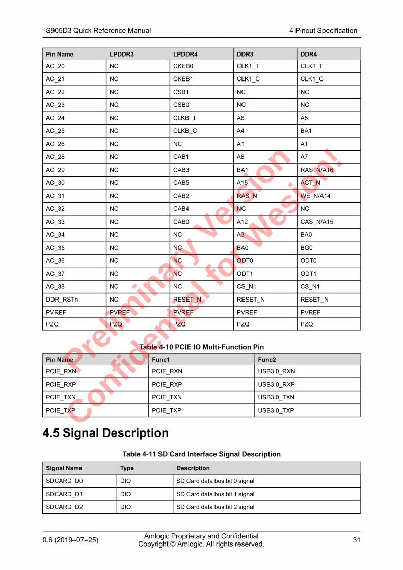
Table 4-9 DDR AC Multi-Function PinPin Name LPDDR3 LPDDR4 DDR3 DDR4
AC_0 CKEA0 CKEA0 CKE0 CKE0
AC_1 CKEA1 CKEA1 CKE1 CKE1
AC_2 CSA0 CSA0 CS_N0 CS_N0
AC_3 CSA1 CSA1 NC NC
AC_4 CLKA_T CLKA_T CAS_N A6
AC_5 CLKA_C CLKA_C BA2 A8
AC_6 NC NC A7 A2
AC_7 NC NC A5 A11
AC_8 CAA2 CAA2 A10 A10
AC_9 CAA7 CAA3 WE_N BG1
AC_10 CAA1 CAA1 A0 A3
AC_11 CAA4 CAA0 A2 A12
AC_12 CAA5 CAA5 A9 A0
AC_13 CAA6 CAA4 A13 A4
AC_14 CAA0 NC A14 A13
AC_15 CAA3 NC A11 A9
AC_16 CAA9 NC CLK0_T CLK0_T
AC_17 CAA8 NC CLK0_C CLK0_C
AC_18 ODTA NC NC NC
S905D3 Quick Reference Manual 4 Pinout Specification
Prelim
inar
y Ver
sion
Confiden
tial f
or Wes
ion!
0.6 (2019–07–25) Amlogic Proprietary and ConfidentialCopyright © Amlogic. All rights reserved. 31
Pin Name LPDDR3 LPDDR4 DDR3 DDR4
AC_20 NC CKEB0 CLK1_T CLK1_T
AC_21 NC CKEB1 CLK1_C CLK1_C
AC_22 NC CSB1 NC NC
AC_23 NC CSB0 NC NC
AC_24 NC CLKB_T A6 A5
AC_25 NC CLKB_C A4 BA1
AC_26 NC NC A1 A1
AC_28 NC CAB1 A8 A7
AC_29 NC CAB3 BA1 RAS_N/A16
AC_30 NC CAB5 A15 ACT_N
AC_31 NC CAB2 RAS_N WE_N/A14
AC_32 NC CAB4 NC NC
AC_33 NC CAB0 A12 CAS_N/A15
AC_34 NC NC A3 BA0
AC_35 NC NC BA0 BG0
AC_36 NC NC ODT0 ODT0
AC_37 NC NC ODT1 ODT1
AC_38 NC NC CS_N1 CS_N1
DDR_RSTn NC RESET_N RESET_N RESET_N
PVREF PVREF PVREF PVREF PVREF
PZQ PZQ PZQ PZQ PZQ
Table 4-10 PCIE IO Multi-Function PinPin Name Func1 Func2
PCIE_RXN PCIE_RXN USB3.0_RXN
PCIE_RXP PCIE_RXP USB3.0_RXP
PCIE_TXN PCIE_TXN USB3.0_TXN
PCIE_TXP PCIE_TXP USB3.0_TXP
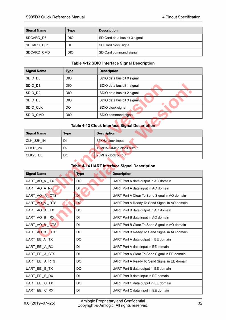
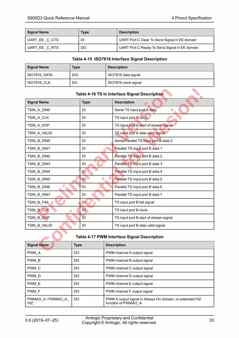
4.5 Signal DescriptionTable 4-11 SD Card Interface Signal Description
Signal Name Type Description
SDCARD_D0 DIO SD Card data bus bit 0 signal
SDCARD_D1 DIO SD Card data bus bit 1 signal
SDCARD_D2 DIO SD Card data bus bit 2 signal
S905D3 Quick Reference Manual 4 Pinout Specification
Prelim
inar
y Ver
sion
Confiden
tial f
or Wes
ion!
0.6 (2019–07–25) Amlogic Proprietary and ConfidentialCopyright © Amlogic. All rights reserved. 32
Signal Name Type Description
SDCARD_D3 DIO SD Card data bus bit 3 signal
SDCARD_CLK DO SD Card clock signal
SDCARD_CMD DIO SD Card command signal
Table 4-12 SDIO Interface Signal Description
Signal Name Type Description
SDIO_D0 DIO SDIO data bus bit 0 signal
SDIO_D1 DIO SDIO data bus bit 1 signal
SDIO_D2 DIO SDIO data bus bit 2 signal
SDIO_D3 DIO SDIO data bus bit 3 signal
SDIO_CLK DO SDIO clock signal
SDIO_CMD DIO SDIO command signal
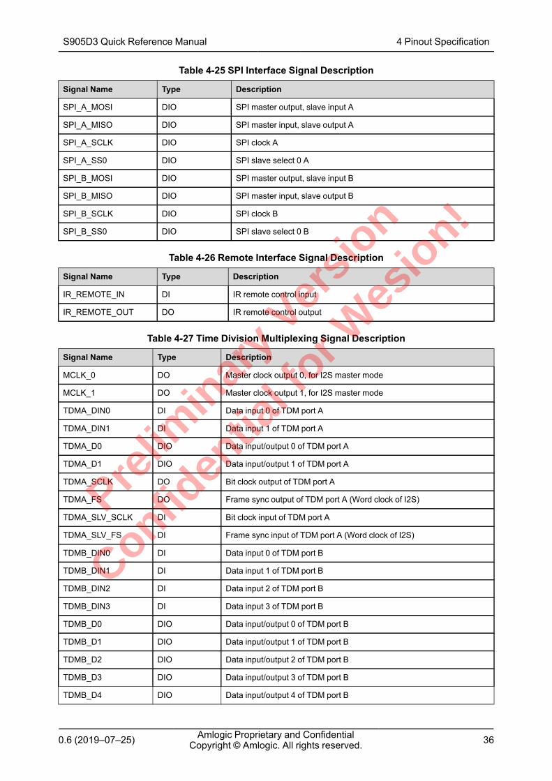
Table 4-13 Clock Interface Signal Description
Signal Name Type Description
CLK_32K_IN DI 32KHz clock input
CLK12_24 DO 12MHz/24MHZ clock output
CLK25_EE DO 25MHz clock output
Table 4-14 UART Interface Signal Description
Signal Name Type Description
UART_AO_A _ TX DO UART Port A data output in AO domain
UART_AO_A_RX DI UART Port A data input in AO domain
UART_AO_ A_ CTS DI UART Port A Clear To Send Signal in AO domain
UART_AO_A _ RTS DO UART Port A Ready To Send Signal in AO domain
UART_AO_B _ TX DO UART Port B data output in AO domain
UART_AO_B _ RX DI UART Port B data input in AO domain
UART_AO_B _ CTS DI UART Port B Clear To Send Signal in AO domain
UART_AO_B _ RTS DO UART Port B Ready To Send Signal in AO domain
UART_EE_A _TX DO UART Port A data output in EE domain
UART_EE _A_RX DI UART Port A data input in EE domain
UART_EE _A_CTS DI UART Port A Clear To Send Signal in EE domain
UART_EE _A_RTS DO UART Port A Ready To Send Signal in EE domain
UART_EE _B_TX DO UART Port B data output in EE domain
UART_EE _B_RX DI UART Port B data input in EE domain
UART_EE _C_TX DO UART Port C data output in EE domain
UART_EE _C_RX DI UART Port C data input in EE domain
S905D3 Quick Reference Manual 4 Pinout Specification
Prelim
inar
y Ver
sion
Confiden
tial f
or Wes
ion!
0.6 (2019–07–25) Amlogic Proprietary and ConfidentialCopyright © Amlogic. All rights reserved. 33
Signal Name Type Description
UART_EE _C_CTS DI UART Port C Clear To Send Signal in EE domain
UART_EE _C_RTS DO UART Port C Ready To Send Signal in EE domain
Table 4-15 ISO7816 Interface Signal Description
Signal Name Type Description
ISO7816_DATA DIO ISO7816 data signal
ISO7816_CLK DO ISO7816 clock signal
Table 4-16 TS In Interface Signal Description
Signal Name Type Description
TSIN_A_DIN0 DI Serial TS input port A data
TSIN_A_CLK DI TS input port A clock
TSIN_A_SOP DI TS input port A start of stream signal
TSIN_A_VALID DI TS input port A date valid signal
TSIN_B_DIN0 DI Serial/Parallel TS input port B data 0
TSIN_B_DIN1 DI Parallel TS input port B data 1
TSIN_B_DIN2 DI Parallel TS input port B data 2
TSIN_B_DIN3 DI Parallel TS input port B data 3
TSIN_B_DIN4 DI Parallel TS input port B data 4
TSIN_B_DIN5 DI Parallel TS input port B data 5
TSIN_B_DIN6 DI Parallel TS input port B data 6
TSIN_B_DIN7 DI Parallel TS input port B data 7
TSIN_B_FAIL DI TS input port B fail signal
TSIN_B_CLK DI TS input port B clock
TSIN_B_SOP DI TS input port B start of stream signal
TSIN_B_VALID DI TS input port B date valid signal
Table 4-17 PWM Interface Signal Description
Signal Name Type Description
PWM_A DO PWM channel A output signal
PWM_B DO PWM channel B output signal
PWM_C DO PWM channel C output signal
PWM_D DO PWM channel D output signal
PWM_E DO PWM channel E output signal
PWM_F DO PWM channel F output signal
PWMAO_A / PWMAO_A_HIZ
DO PWM A output signal in Always On domain, or extended HiZfunction of PWMAO_A
S905D3 Quick Reference Manual 4 Pinout Specification
Prelim
inar
y Ver
sion
Confiden
tial f
or Wes
ion!

0.6 (2019–07–25) Amlogic Proprietary and ConfidentialCopyright © Amlogic. All rights reserved. 34
Signal Name Type Description
PWMAO_B DO PWM B output signal in Always On domain
PWMAO_C / PWMAO_C_HIZ
DO PWM C output signal in Always On domain, or extended HiZfunction of PWMAO_C
PWMAO_D DO PWM D output signal in Always On domain
Table 4-18 I2C Interface Signal Description
Signal Name Type Description
I2C_AO_ M0_ SCL DO I2C bus port 0 clock output, Master mode, in AO domain
I2C_AO _M0_SDA DIO I2C bus port 0 data input/output, Master mode, in AO domain
I2C_AO_S0_SCL DI I2C bus port 0 clock input, Slave mode, in AO domain
I2C_AO_S0_SDA DIO I2C bus port 0 data input/output, Slave mode, in AO domain
I2C_EE_M0_SCL DO I2C bus port 0 clock output, Master mode, in EE domain
I2C_EE _M0_SDA DIO I2C bus port 0 data input/output, Master mode, in EE domain
I2C_EE_M1_SCL DO I2C bus port 1 clock output, Master mode, in EE domain
I2C_EE _M1_SDA DIO I2C bus port 1 data input/output, Master mode, in EE domain
I2C_EE_M2_SCL DO I2C bus port 2 clock output, Master mode, in EE domain
I2C_EE _M2_SDA DIO I2C bus port 2 data input/output, Master mode, in EE domain
I2C_EE_M3_SCL DO I2C bus port 3 clock output, Master mode, in EE domain
I2C_EE_M3_SDA DIO I2C bus port 3 data input/output, Master mode, in EE domain
Table 4-19 eMMC Interface Signal Description
Signal Name Type Description
EMMC_D0 DIO eMMC/NAND data bus bit 0 signal
EMMC_D1 DIO eMMC/NAND data bus bit 1 signal
EMMC_D2 DIO eMMC/NAND data bus bit 2 signal
EMMC_D3 DIO eMMC/NAND data bus bit 3 signal
EMMC_D4 DIO eMMC/NAND data bus bit 4 signal
EMMC_D5 DIO eMMC/NAND data bus bit 5 signal
EMMC_D6 DIO eMMC/NAND data bus bit 6 signal
EMMC_D7 DIO eMMC/NAND data bus bit 7 signal
EMMC_CLK DO eMMC clock signal
EMMC_CMD DIO eMMC command signal
EMMC_NAND_DQS DIO eMMC/NAND data strobe
S905D3 Quick Reference Manual 4 Pinout Specification
Prelim
inar
y Ver
sion
Confiden
tial f
or Wes
ion!
0.6 (2019–07–25) Amlogic Proprietary and ConfidentialCopyright © Amlogic. All rights reserved. 35
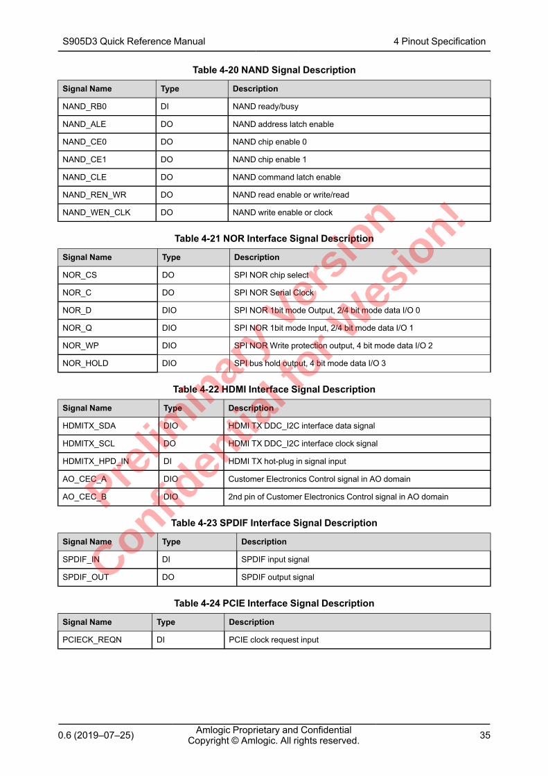
Table 4-20 NAND Signal Description
Signal Name Type Description
NAND_RB0 DI NAND ready/busy
NAND_ALE DO NAND address latch enable
NAND_CE0 DO NAND chip enable 0
NAND_CE1 DO NAND chip enable 1
NAND_CLE DO NAND command latch enable
NAND_REN_WR DO NAND read enable or write/read
NAND_WEN_CLK DO NAND write enable or clock
Table 4-21 NOR Interface Signal Description
Signal Name Type Description
NOR_CS DO SPI NOR chip select
NOR_C DO SPI NOR Serial Clock
NOR_D DIO SPI NOR 1bit mode Output, 2/4 bit mode data I/O 0
NOR_Q DIO SPI NOR 1bit mode Input, 2/4 bit mode data I/O 1
NOR_WP DIO SPI NORWrite protection output, 4 bit mode data I/O 2
NOR_HOLD DIO SPI bus hold output, 4 bit mode data I/O 3
Table 4-22 HDMI Interface Signal Description
Signal Name Type Description
HDMITX_SDA DIO HDMI TX DDC_I2C interface data signal
HDMITX_SCL DO HDMI TX DDC_I2C interface clock signal
HDMITX_HPD_IN DI HDMI TX hot-plug in signal input
AO_CEC_A DIO Customer Electronics Control signal in AO domain
AO_CEC_B DIO 2nd pin of Customer Electronics Control signal in AO domain
Table 4-23 SPDIF Interface Signal Description
Signal Name Type Description
SPDIF_IN DI SPDIF input signal
SPDIF_OUT DO SPDIF output signal
Table 4-24 PCIE Interface Signal Description
Signal Name Type Description
PCIECK_REQN DI PCIE clock request input
S905D3 Quick Reference Manual 4 Pinout Specification
Prelim
inar
y Ver
sion
Confiden
tial f
or Wes
ion!
0.6 (2019–07–25) Amlogic Proprietary and ConfidentialCopyright © Amlogic. All rights reserved. 36
Table 4-25 SPI Interface Signal Description
Signal Name Type Description
SPI_A_MOSI DIO SPI master output, slave input A
SPI_A_MISO DIO SPI master input, slave output A
SPI_A_SCLK DIO SPI clock A
SPI_A_SS0 DIO SPI slave select 0 A
SPI_B_MOSI DIO SPI master output, slave input B
SPI_B_MISO DIO SPI master input, slave output B
SPI_B_SCLK DIO SPI clock B
SPI_B_SS0 DIO SPI slave select 0 B
Table 4-26 Remote Interface Signal Description
Signal Name Type Description
IR_REMOTE_IN DI IR remote control input
IR_REMOTE_OUT DO IR remote control output
Table 4-27 Time Division Multiplexing Signal Description
Signal Name Type Description
MCLK_0 DO Master clock output 0, for I2S master mode
MCLK_1 DO Master clock output 1, for I2S master mode
TDMA_DIN0 DI Data input 0 of TDM port A
TDMA_DIN1 DI Data input 1 of TDM port A
TDMA_D0 DIO Data input/output 0 of TDM port A
TDMA_D1 DIO Data input/output 1 of TDM port A
TDMA_SCLK DO Bit clock output of TDM port A
TDMA_FS DO Frame sync output of TDM port A (Word clock of I2S)
TDMA_SLV_SCLK DI Bit clock input of TDM port A
TDMA_SLV_FS DI Frame sync input of TDM port A (Word clock of I2S)
TDMB_DIN0 DI Data input 0 of TDM port B
TDMB_DIN1 DI Data input 1 of TDM port B
TDMB_DIN2 DI Data input 2 of TDM port B
TDMB_DIN3 DI Data input 3 of TDM port B
TDMB_D0 DIO Data input/output 0 of TDM port B
TDMB_D1 DIO Data input/output 1 of TDM port B
TDMB_D2 DIO Data input/output 2 of TDM port B
TDMB_D3 DIO Data input/output 3 of TDM port B
TDMB_D4 DIO Data input/output 4 of TDM port B
S905D3 Quick Reference Manual 4 Pinout Specification
Prelim
inar
y Ver
sion
Confiden
tial f
or Wes
ion!
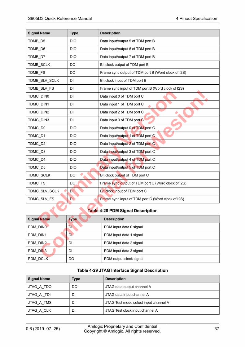
0.6 (2019–07–25) Amlogic Proprietary and ConfidentialCopyright © Amlogic. All rights reserved. 37
Signal Name Type Description
TDMB_D5 DIO Data input/output 5 of TDM port B
TDMB_D6 DIO Data input/output 6 of TDM port B
TDMB_D7 DIO Data input/output 7 of TDM port B
TDMB_SCLK DO Bit clock output of TDM port B
TDMB_FS DO Frame sync output of TDM port B (Word clock of I2S)
TDMB_SLV_SCLK DI Bit clock input of TDM port B
TDMB_SLV_FS DI Frame sync input of TDM port B (Word clock of I2S)
TDMC_DIN0 DI Data input 0 of TDM port C
TDMC_DIN1 DI Data input 1 of TDM port C
TDMC_DIN2 DI Data input 2 of TDM port C
TDMC_DIN3 DI Data input 3 of TDM port C
TDMC_D0 DIO Data input/output 0 of TDM port C
TDMC_D1 DIO Data input/output 1 of TDM port C
TDMC_D2 DIO Data input/output 2 of TDM port C
TDMC_D3 DIO Data input/output 3 of TDM port C
TDMC_D4 DIO Data input/output 4 of TDM port C
TDMC_D5 DIO Data input/output 5 of TDM port C
TDMC_SCLK DO Bit clock output of TDM port C
TDMC_FS DO Frame sync output of TDM port C (Word clock of I2S)
TDMC_SLV_SCLK DI Bit clock input of TDM port C
TDMC_SLV_FS DI Frame sync input of TDM port C (Word clock of I2S)
Table 4-28 PDM Signal Description
Signal Name Type Description
PDM_DIN0 DI PDM input data 0 signal
PDM_DIN1 DI PDM input data 1 signal
PDM_DIN2 DI PDM input data 2 signal
PDM_DIN3 DI PDM input data 3 signal
PDM_DCLK DO PDM output clock signal
Table 4-29 JTAG Interface Signal Description
Signal Name Type Description
JTAG_A_TDO DO JTAG data output channel A
JTAG_A _TDI DI JTAG data input channel A
JTAG_A_TMS DI JTAG Test mode select input channel A
JTAG_A_CLK DI JTAG Test clock input channel A
S905D3 Quick Reference Manual 4 Pinout Specification
Prelim
inar
y Ver
sion
Confiden
tial f
or Wes
ion!
0.6 (2019–07–25) Amlogic Proprietary and ConfidentialCopyright © Amlogic. All rights reserved. 38
Signal Name Type Description
JTAG_B_TDO DO JTAG data output channel B
JTAG_B _TDI DI JTAG data input channel B
JTAG_B_TMS DI JTAG Test mode select input channel B
JTAG_B _CLK DI JTAG Test clock input channel B
Table 4-30 Ethernet Interface Signal Description
Signal Name Type Description
ETH_LINK_LED DO Ethernet link LED indicator
ETH_ACT_LED DO Ethernet active LED indicator
ETH_RGMII_RX_CLK DI Ethernet RGMII interface receive clock input
ETH_RGMII_TX_CLK DO Ethernet RGMII transmit clock
ETH_TX_EN DO Ethernet RMII/RGMII Interface transmit enable
ETH_TXD3_RGMII DO Ethernet RGMII interface transmit data 3
ETH_TXD2_RGMII DO Ethernet RGMII interface transmit data 2
ETH_TXD1 DO Ethernet RMII/RGMII interface transmit data 1
ETH_TXD0 DO Ethernet RMII/RGMII interface transmit data 0
ETH_RX_DV DI Ethernet RMII/RGMII interface receive data valid signal
ETH_RXD3_RGMII DI Ethernet RGMII interface receive data 3
ETH_RXD2_RGMII DI Ethernet RGMII interface receive data 2
ETH_RXD1 DI Ethernet RMII/RGMII interface receive data 1
ETH_RXD0 DI Ethernet RMII/RGMII interface receive data 0
ETH_MDIO DIO Ethernet SMI interface management data input/output
ETH_MDC DO Ethernet SMI interface management clock
Table 4-31 Other Signal Description
Signal Name Type Description
WORLD_SYNC DI World clock sync input, to sync clock of multi devices
GEN_CLK_EE DO General clock output for EE domain clock, for debug
GEN_CLK_AO DO General clock output for AO domain clock, for debug
S905D3 Quick Reference Manual 4 Pinout Specification
Prelim
inar
y Ver
sion
Confiden
tial f
or Wes
ion!
0.6 (2019–07–25) Amlogic Proprietary and ConfidentialCopyright © Amlogic. All rights reserved. 39
5 Operating Conditions5.1 Absolute Maximum RatingsThe table below gives the absolute maximum ratings. Exposure to stresses beyond those listed in thistable may result in permanent device damage, unreliability or both.
Characteristic Value Unit
VDDCPU Supply Voltage 1.1 V
VDD_EE Supply Voltage 1.0 V
VDDQ Supply Voltage 1.7 V
AVDD_DDRPLL 1.98 V
1.8V Supply Voltage 1.98 V
3.3V Supply Voltage 3.63 V
Input voltage, VI -0.3 ~ VDDIO+0.3 V
Junction Temperature 125 °C
5.2 Recommended Operating Conditions
Symbol Parameter Min. Typ. Max Unit
VDDCPU Voltage for Cortex A55 CPU 0.681 - 1.032 V
VDD_EE and other0.8V domain
Voltage for GPU & core logic 0.77 0.8 0.9 V
VDDQ DDR3/DDR3L/DDR4/LPDDR/LPDDR3/LPDDR4 IO Supply Voltage
1.05 - 1.6 V
AVDD18 1.8VAVDD for HDMI, USB, SARADC,PCIE, CVBS, ETHERNET phy,MIPI_DSI, MIPI_CSI and AUDIO
1.71 1.80 1.89 V
VDD18_AO_XTAL 1.8V VDD for XTAL, and IOVREF 1.71 1.80 1.89 V
AVDD_DDRPLL Analog power supply for DDRPLL 1.05 - 1.89 V
AVDD33 3.3VAVDD for USB 3.15 3.3 3.45 V
VDDIO LV mode 1.71 1.80 1.89 V
HV mode 3.03 3.3 3.45 V
TJ Operating Junction Temperature 0 — 1054 °C
TA Operating Ambient Temperature 0 — 70 °C
S905D3 Quick Reference Manual 5 Operating Conditions
Prelim
inar
y Ver
sion
Confiden
tial f
or Wes
ion!
0.6 (2019–07–25) Amlogic Proprietary and ConfidentialCopyright © Amlogic. All rights reserved. 40
Note1. Minimal VDDCPU voltage is for sleep mode while system runs at very low speed. Higher
clock will need higher voltage. Considering the power supply may have 3% deviation, theminimal voltage in actual application should not be set to lower than min spec plus 0.02V.
2. Likewise, maximum VDDCPU voltage in actual application should be lower than the maxspec value minus 0.02V. Voltage of VDDCPU will affect CPU speed. Use lower voltage whenCPU runs on lower speed to save power. Recommend to use +/-1.5% or higher precisionDCDC.
3. GPIO cannot work if VDDIO voltage is out of the spec of LV / HV mode. GPIO output at HVmode will be weaker & max operating speed will be lower if VDDIO are design to 3.0V. Donot design VDDIO to lower than 3.0V in HV mode, recommend to use +/-1.5% or higher pre-cision DCDC to supply power for VDDIO, actual voltage supplies to VDDIO (HV mode)should not be lower than 2.9V.
4. For operating temperature, good heat sink may be needed to guarantee Tj < max spec.
5.3 Ripple Voltage SpecificationsPlease check below table for ripple voltage specifications.
Power Max Ripple Unit Test State
VDDCPU 40 +/-mV Run APK StabilityTest
VDD_EE and other 0.8Vdomain
40 +/-mV Run APK Basemark ES2.0 Taiji
DDR3 VDDQ and AVDD_DDRPLL
60 +/-mV Kernel boot
DDR3LVDDQ and AVDD_DDRPLL
60 +/-mV Kernel boot
LPDDR3 VDDQ andAVDD_DDRPLL
40 +/-mV Kernel boot
DDR4 VDDQ and AVDD_DDRPLL
40 +/-mV Kernel boot
LPDDR4 VDDQ andAVDD_DDRPLL
40 +/-mV Kernel boot
AVDD18 30 +/-mV Kernel boot
VDD18_AO_XTAL 30 +/-mV Kernel boot
AVDD33 50 +/-mV WIFI SCAN
VDDIO LV 60 +/-mV Kernel boot
VDDIO HV 60 +/-mV WIFI SCAN
NoteRipple specification is only a reference spec, customer should run stress/performance/reliabilitytest (high/low temperature test, damp and hot test, function test, etc...) on their product toconfirm the system stability.
5.4 Thermal Resistance
S905D3 Quick Reference Manual 5 Operating Conditions
Prelim
inar
y Ver
sion
Confiden
tial f
or Wes
ion!
0.6 (2019–07–25) Amlogic Proprietary and ConfidentialCopyright © Amlogic. All rights reserved. 41
Jedec 2P2S board 101.5mm*114.5mm,natural convection, ambient temperature 25°C.
Symbol Parameter Value(°C/Watt)
Air Flow(m/s)
Θja Package junction-to- ambiance thermal resistance in natureconvection
16.92 0
Θjb Package junction-to-pcb thermal resistance in natureconvection
8.13 0
Θjc Package junction-to-case thermal resistance in natureconvection
7.25 0
Note1. Due to the thinness of the SOC, DRAM or capacitors placed close to SOC may prevent
heatsink touching SOC top side. A special convex shape heatsink is recommended.2. These measurement were conducted on a JEDEC defined 2S2P system. For more
information, check below JEDEC standards:
●● JESD51-2A: Integrated Circuits Thermal Test Method Environmental Conditions - NaturalConvection (Still Air)
●● JESD51-8:Integrated Circuit Thermal Test Method Environmental Conditions —Junction-to-Board
●● JESD51-12:Guidelines for Reporting and Using Electronic Package Thermal Information3. m/s = meters per second
5.5 DC Electrical Characteristics
5.5.1 Normal GPIO Specifications (For DIO_xmA)
Symbol Parameter Min. Typ. Max. Unit
ViH(VDDIO=3.3V)3 High-level inputvoltage
IOVREF+0.37 - VDDIO+0.3 V
ViL(VDDIO=3.3V)3 Low-level inputvoltage
-0.3 - IOVREF-0.23 V
ViH(VDDIO=1.8V)3 High-level inputvoltage
IOVREF/2+0.3 - VDDIO+0.3 V
ViL(VDDIO=1.8V)3 Low-level inputvoltage
-0.3 - IOVREF/2-0.3 V
RPU Built-in pull upresistor
50K 60K 70K ohm
RPD Built-in pull downresistor
50K5 60K 130K6 ohm
IoL/IoH(DS=0)1,4 GPIO drivingcapability
0.5 - - mA
IoL/IoH(DS=1)1 GPIO drivingcapability
2.5 - - mA
IoL/IoH(DS=2)1 GPIO drivingcapability
3 - - mA
S905D3 Quick Reference Manual 5 Operating Conditions
Prelim
inar
y Ver
sion
Confiden
tial f
or Wes
ion!
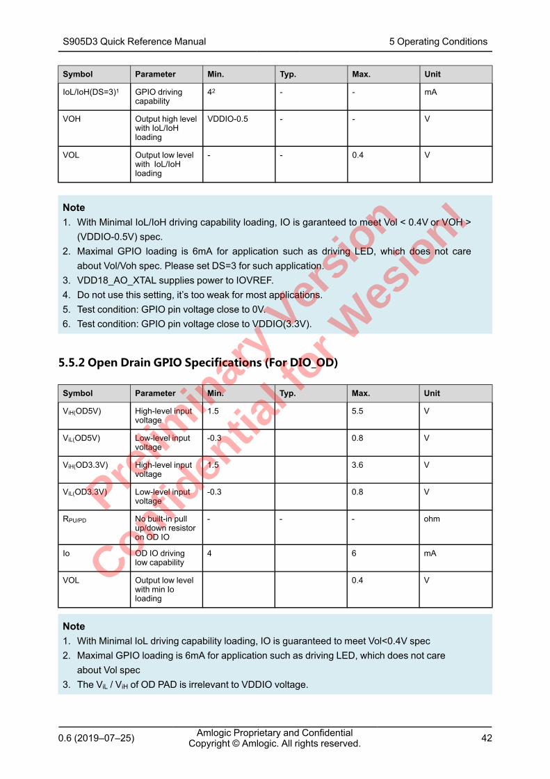
0.6 (2019–07–25) Amlogic Proprietary and ConfidentialCopyright © Amlogic. All rights reserved. 42
Symbol Parameter Min. Typ. Max. Unit
IoL/IoH(DS=3)1 GPIO drivingcapability
42 - - mA
VOH Output high levelwith IoL/IoHloading
VDDIO-0.5 - - V
VOL Output low levelwith IoL/IoHloading
- - 0.4 V
Note1. With Minimal IoL/IoH driving capability loading, IO is garanteed to meet Vol < 0.4V or VOH >
(VDDIO-0.5V) spec.2. Maximal GPIO loading is 6mA for application such as driving LED, which does not care
about Vol/Voh spec. Please set DS=3 for such application.3. VDD18_AO_XTAL supplies power to IOVREF.4. Do not use this setting, it’s too weak for most applications.5. Test condition: GPIO pin voltage close to 0V.6. Test condition: GPIO pin voltage close to VDDIO(3.3V).
5.5.2 Open Drain GPIO Specifications (For DIO_OD)
Symbol Parameter Min. Typ. Max. Unit
ViH(OD5V) High-level inputvoltage
1.5 5.5 V
ViL(OD5V) Low-level inputvoltage
-0.3 0.8 V
ViH(OD3.3V) High-level inputvoltage
1.5 3.6 V
ViL(OD3.3V) Low-level inputvoltage
-0.3 0.8 V
RPU/PD No built-in pullup/down resistoron OD IO
- - - ohm
Io OD IO drivinglow capability
4 6 mA
VOL Output low levelwith min Ioloading
0.4 V
Note1. With Minimal IoL driving capability loading, IO is guaranteed to meet Vol<0.4V spec2. Maximal GPIO loading is 6mA for application such as driving LED, which does not care
about Vol spec3. The ViL / ViH of OD PAD is irrelevant to VDDIO voltage.
S905D3 Quick Reference Manual 5 Operating Conditions
Prelim
inar
y Ver
sion
Confiden
tial f
or Wes
ion!
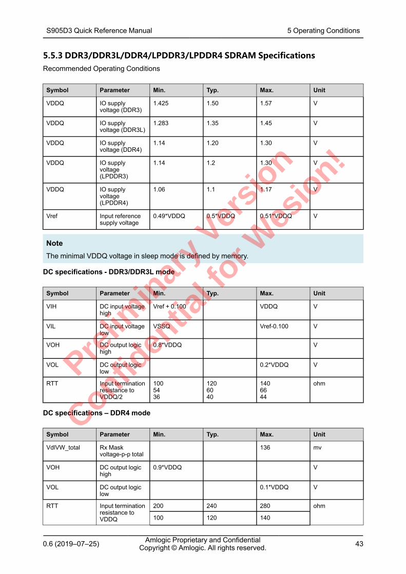
0.6 (2019–07–25) Amlogic Proprietary and ConfidentialCopyright © Amlogic. All rights reserved. 43
5.5.3 DDR3/DDR3L/DDR4/LPDDR3/LPDDR4 SDRAM SpecificationsRecommended Operating Conditions
Symbol Parameter Min. Typ. Max. Unit
VDDQ IO supplyvoltage (DDR3)
1.425 1.50 1.57 V
VDDQ IO supplyvoltage (DDR3L)
1.283 1.35 1.45 V
VDDQ IO supplyvoltage (DDR4)
1.14 1.20 1.30 V
VDDQ IO supplyvoltage(LPDDR3)
1.14 1.2 1.30 V
VDDQ IO supplyvoltage(LPDDR4)
1.06 1.1 1.17 V
Vref Input referencesupply voltage
0.49*VDDQ 0.5*VDDQ 0.51*VDDQ V
NoteThe minimal VDDQ voltage in sleep mode is defined by memory.
DC specifications - DDR3/DDR3L mode
Symbol Parameter Min. Typ. Max. Unit
VIH DC input voltagehigh
Vref + 0.100 VDDQ V
VIL DC input voltagelow
VSSQ Vref-0.100 V
VOH DC output logichigh
0.8*VDDQ V
VOL DC output logiclow
0.2*VDDQ V
RTT Input terminationresistance toVDDQ/2
1005436
1206040
1406644
ohm
DC specifications – DDR4 mode
Symbol Parameter Min. Typ. Max. Unit
VdlVW_total Rx Maskvoltage-p-p total
136 mv
VOH DC output logichigh
0.9*VDDQ V
VOL DC output logiclow
0.1*VDDQ V
RTT Input terminationresistance toVDDQ
200 240 280 ohm
100 120 140
S905D3 Quick Reference Manual 5 Operating Conditions
Prelim
inar
y Ver
sion
Confiden
tial f
or Wes
ion!
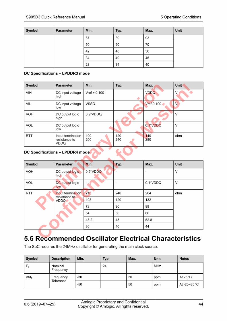
0.6 (2019–07–25) Amlogic Proprietary and ConfidentialCopyright © Amlogic. All rights reserved. 44
Symbol Parameter Min. Typ. Max. Unit
67 80 93
50 60 70
42 48 56
34 40 46
28 34 40
DC Specifications – LPDDR3 mode
Symbol Parameter Min. Typ. Max. Unit
VIH DC input voltagehigh
Vref + 0.100 VDDQ V
VIL DC input voltagelow
VSSQ Vref-0.100 V
VOH DC output logichigh
0.9*VDDQ V
VOL DC output logiclow
0.1*VDDQ V
RTT Input terminationresistance toVDDQ
100200
120240
140280
ohm
DC Specifications – LPDDR4 mode
Symbol Parameter Min. Typ. Max. Unit
VOH DC output logichigh
0.9*VDDQ - - V
VOL DC output logiclow
- - 0.1*VDDQ V
RTT Input terminationresistance toVDDQ
216 240 264 ohm
108 120 132
72 80 88
54 60 66
43.2 48 52.8
36 40 44
5.6 Recommended Oscillator Electrical CharacteristicsThe SoC requires the 24MHz oscillator for generating the main clock source.
Symbol Description Min. Typ. Max. Unit Notes
Fo NominalFrequency
24 MHz
Δf/fo FrequencyTolerance
-30 30 ppm At 25℃
-50 50 ppm At -20~85℃
S905D3 Quick Reference Manual 5 Operating Conditions
Prelim
inar
y Ver
sion
Confiden
tial f
or Wes
ion!
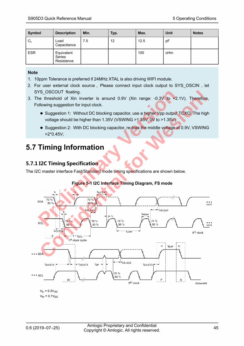
0.6 (2019–07–25) Amlogic Proprietary and ConfidentialCopyright © Amlogic. All rights reserved. 45
Symbol Description Min. Typ. Max. Unit Notes
CL LoadCapacitance
7.5 12 12.5 pF
ESR EquivalentSeriesResistance
100 oHm
Note1. 10ppm Tolerance is preferred if 24MHz XTAL is also driving WIFI module.2. For user external clock source, Please connect input clock output to SYS_OSCIN , let
SYS_OSCOUT floating.3. The threshold of Xin inverter is around 0.9V (Xin range: -0.3V to +2.1V). Therefore,
Following suggestion for input clock.
●● Suggestion 1: Without DC blocking capacitor, use a higher Vpp output TCXO. The highvoltage should be higher than 1.35V (VSWING >1.35V, 0V to >1.35V).
●● Suggestion 2: With DC blocking capacitor, re-bias the middle voltage at 0.9V, VSWING>2*0.45V;
5.7 Timing Information
5.7.1 I2C Timing SpecificationThe I2C master interface Fast/Standard mode timing specifications are shown below.
Figure 5-1 I2C Interface Timing Diagram, FS mode
S905D3 Quick Reference Manual 5 Operating Conditions
Prelim
inar
y Ver
sion
Confiden
tial f
or Wes
ion!
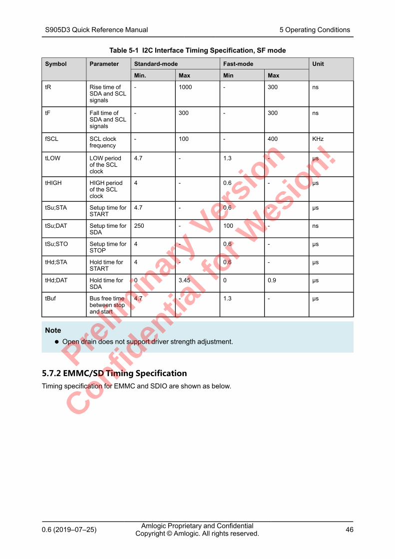
0.6 (2019–07–25) Amlogic Proprietary and ConfidentialCopyright © Amlogic. All rights reserved. 46
Table 5-1 I2C Interface Timing Specification, SF mode
Symbol Parameter Standard-mode Fast-mode Unit
Min. Max Min Max
tR Rise time ofSDA and SCLsignals
- 1000 - 300 ns
tF Fall time ofSDA and SCLsignals
- 300 - 300 ns
fSCL SCL clockfrequency
- 100 - 400 KHz
tLOW LOW periodof the SCLclock
4.7 - 1.3 - µs
tHIGH HIGH periodof the SCLclock
4 - 0.6 - µs
tSu;STA Setup time forSTART
4.7 - 0.6 - µs
tSu;DAT Setup time forSDA
250 - 100 - ns
tSu;STO Setup time forSTOP
4 - 0.6 - µs
tHd;STA Hold time forSTART
4 - 0.6 - µs
tHd;DAT Hold time forSDA
0 3.45 0 0.9 µs
tBuf Bus free timebetween stopand start
4.7 - 1.3 - µs
Note●● Open drain does not support driver strength adjustment.
5.7.2 EMMC/SD Timing SpecificationTiming specification for EMMC and SDIO are shown as below.
S905D3 Quick Reference Manual 5 Operating Conditions
Prelim
inar
y Ver
sion
Confiden
tial f
or Wes
ion!
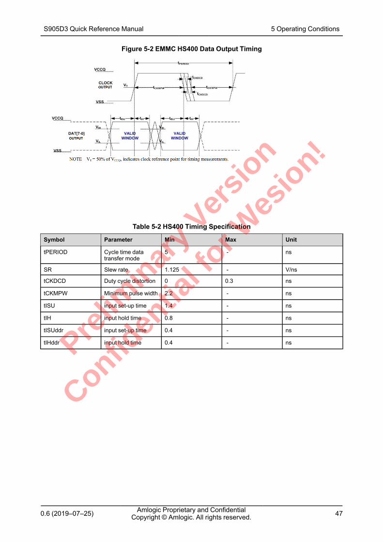
0.6 (2019–07–25) Amlogic Proprietary and ConfidentialCopyright © Amlogic. All rights reserved. 47
Figure 5-2 EMMC HS400 Data Output Timing
Table 5-2 HS400 Timing Specification
Symbol Parameter Min Max Unit
tPERIOD Cycle time datatransfer mode
5 - ns
SR Slew rate 1.125 - V/ns
tCKDCD Duty cycle distortion 0 0.3 ns
tCKMPW Minimum pulse width 2.2 - ns
tISU input set-up time 1.4 - ns
tIH input hold time 0.8 - ns
tISUddr input set-up time 0.4 - ns
tIHddr input hold time 0.4 - ns
S905D3 Quick Reference Manual 5 Operating Conditions
Prelim
inar
y Ver
sion
Confiden
tial f
or Wes
ion!
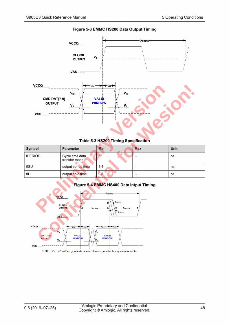
0.6 (2019–07–25) Amlogic Proprietary and ConfidentialCopyright © Amlogic. All rights reserved. 48
Figure 5-3 EMMC HS200 Data Output Timing
Table 5-3 HS200 Timing Specification
Symbol Parameter Min Max Unit
tPERIOD Cycle time datatransfer mode
5 - ns
tISU output set-up time 1.4 - ns
tIH output hold time 0.8 - ns
Figure 5-4 EMMC HS400 Data Intput Timing
S905D3 Quick Reference Manual 5 Operating Conditions
Prelim
inar
y Ver
sion
Confiden
tial f
or Wes
ion!
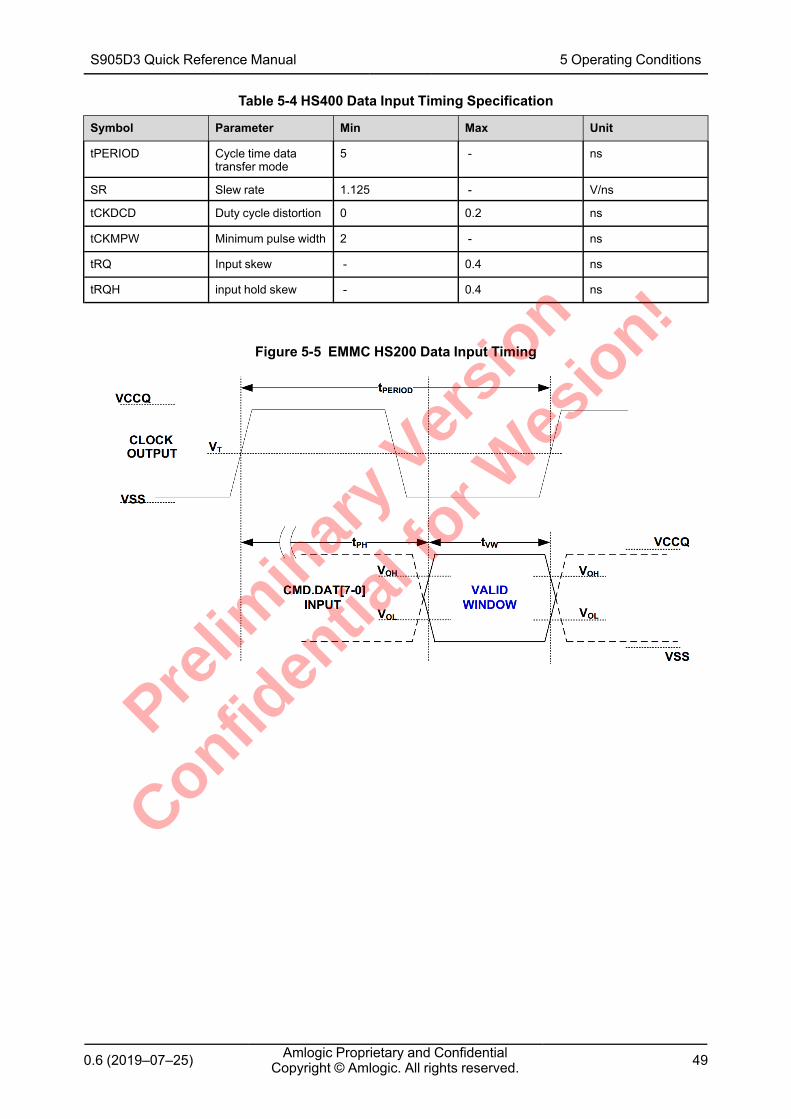
0.6 (2019–07–25) Amlogic Proprietary and ConfidentialCopyright © Amlogic. All rights reserved. 49
Table 5-4 HS400 Data Input Timing Specification
Symbol Parameter Min Max Unit
tPERIOD Cycle time datatransfer mode
5 - ns
SR Slew rate 1.125 - V/ns
tCKDCD Duty cycle distortion 0 0.2 ns
tCKMPW Minimum pulse width 2 - ns
tRQ Input skew - 0.4 ns
tRQH input hold skew - 0.4 ns
Figure 5-5 EMMC HS200 Data Input Timing
S905D3 Quick Reference Manual 5 Operating Conditions
Prelim
inar
y Ver
sion
Confiden
tial f
or Wes
ion!
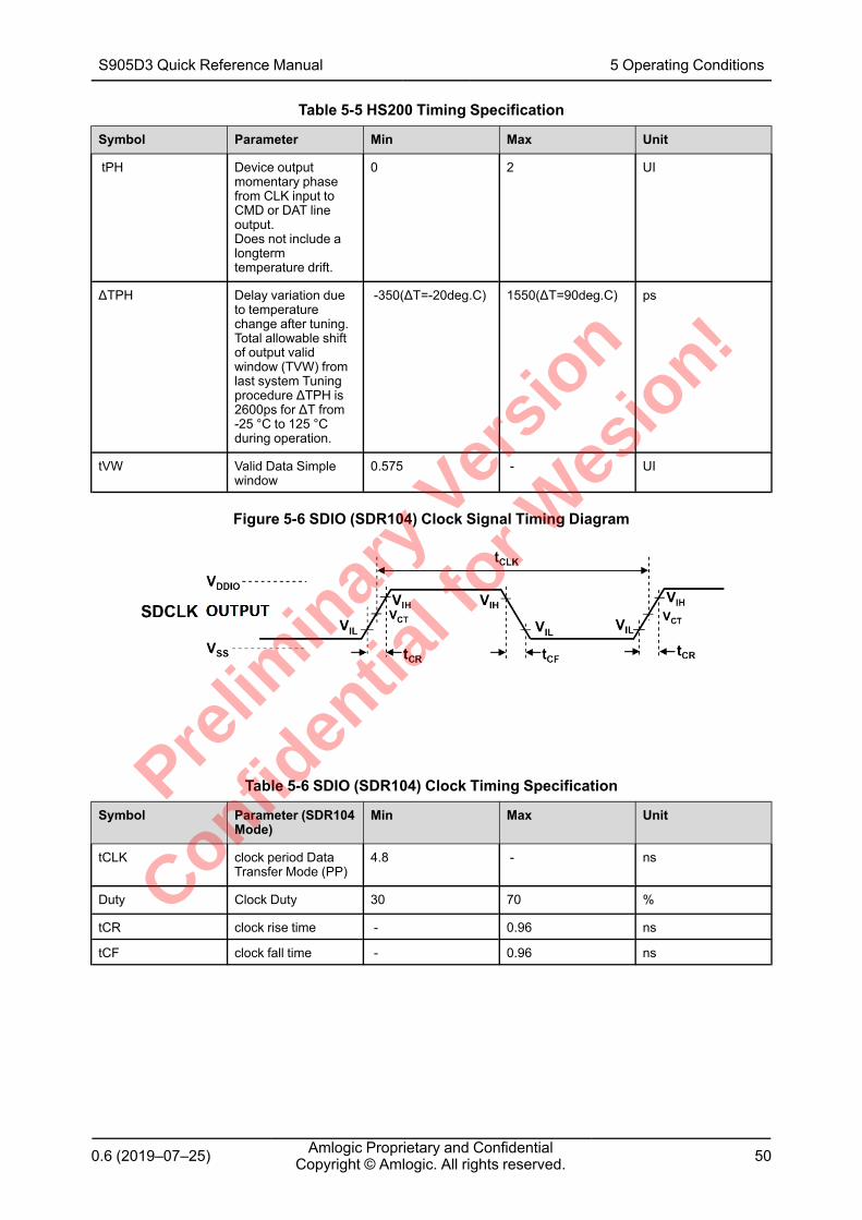
0.6 (2019–07–25) Amlogic Proprietary and ConfidentialCopyright © Amlogic. All rights reserved. 50
Table 5-5 HS200 Timing Specification
Symbol Parameter Min Max Unit
tPH Device outputmomentary phasefrom CLK input toCMD or DAT lineoutput.Does not include alongtermtemperature drift.
0 2 UI
ΔTPH Delay variation dueto temperaturechange after tuning.Total allowable shiftof output validwindow (TVW) fromlast system Tuningprocedure ΔTPH is2600ps for ΔT from-25 °C to 125 °Cduring operation.
-350(ΔT=-20deg.C) 1550(ΔT=90deg.C) ps
tVW Valid Data Simplewindow
0.575 - UI
Figure 5-6 SDIO (SDR104) Clock Signal Timing Diagram
Table 5-6 SDIO (SDR104) Clock Timing Specification
Symbol Parameter (SDR104Mode)
Min Max Unit
tCLK clock period DataTransfer Mode (PP)
4.8 - ns
Duty Clock Duty 30 70 %
tCR clock rise time - 0.96 ns
tCF clock fall time - 0.96 ns
S905D3 Quick Reference Manual 5 Operating Conditions
Prelim
inar
y Ver
sion
Confiden
tial f
or Wes
ion!
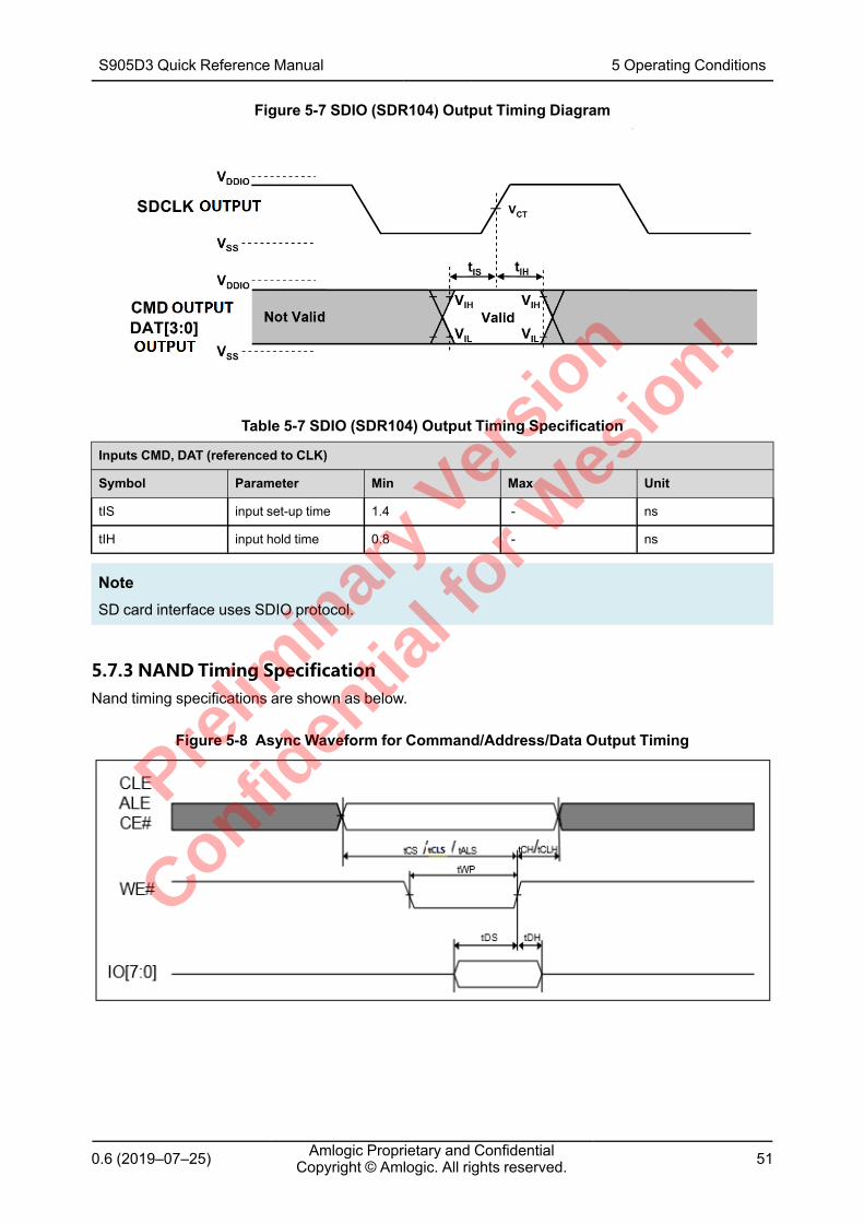
0.6 (2019–07–25) Amlogic Proprietary and ConfidentialCopyright © Amlogic. All rights reserved. 51
Figure 5-7 SDIO (SDR104) Output Timing Diagram
Table 5-7 SDIO (SDR104) Output Timing Specification
Inputs CMD, DAT (referenced to CLK)
Symbol Parameter Min Max Unit
tIS input set-up time 1.4 - ns
tIH input hold time 0.8 - ns
NoteSD card interface uses SDIO protocol.
5.7.3 NAND Timing SpecificationNand timing specifications are shown as below.
Figure 5-8 Async Waveform for Command/Address/Data Output Timing
S905D3 Quick Reference Manual 5 Operating Conditions
Prelim
inar
y Ver
sion
Confiden
tial f
or Wes
ion!
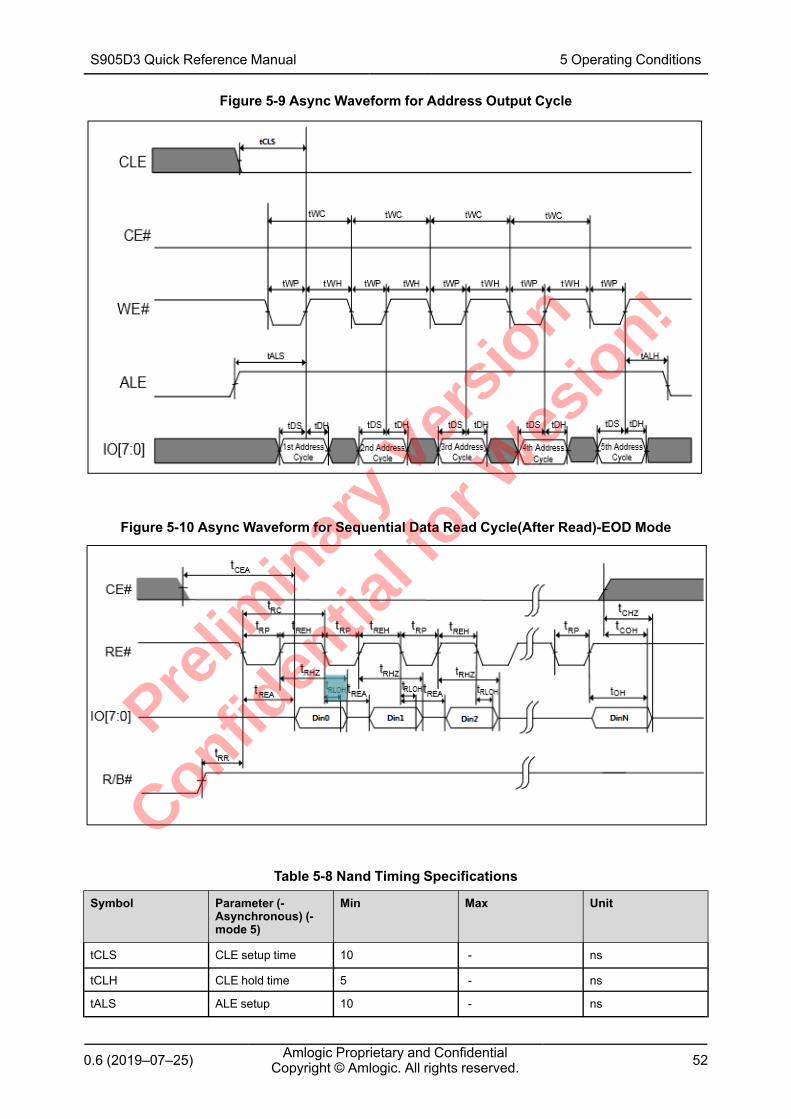
0.6 (2019–07–25) Amlogic Proprietary and ConfidentialCopyright © Amlogic. All rights reserved. 52
Figure 5-9 Async Waveform for Address Output Cycle
Figure 5-10 Async Waveform for Sequential Data Read Cycle(After Read)-EOD Mode
Table 5-8 Nand Timing Specifications
Symbol Parameter (-Asynchronous) (-mode 5)
Min Max Unit
tCLS CLE setup time 10 - ns
tCLH CLE hold time 5 - ns
tALS ALE setup 10 - ns
S905D3 Quick Reference Manual 5 Operating Conditions
Prelim
inar
y Ver
sion
Confiden
tial f
or Wes
ion!
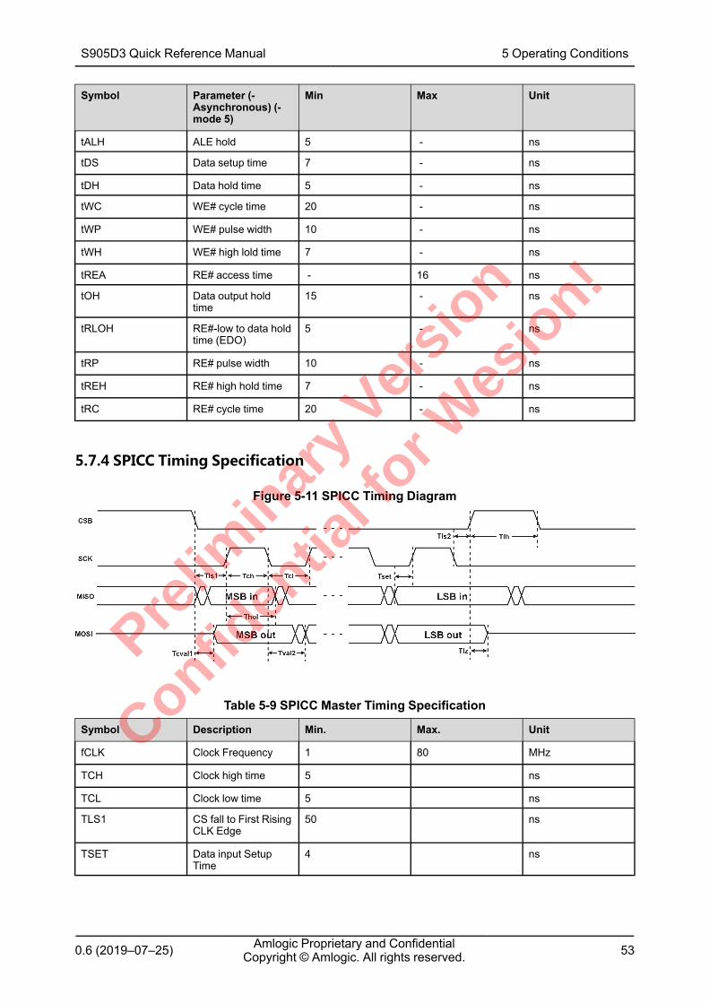
0.6 (2019–07–25) Amlogic Proprietary and ConfidentialCopyright © Amlogic. All rights reserved. 53
Symbol Parameter (-Asynchronous) (-mode 5)
Min Max Unit
tALH ALE hold 5 - ns
tDS Data setup time 7 - ns
tDH Data hold time 5 - ns
tWC WE# cycle time 20 - ns
tWP WE# pulse width 10 - ns
tWH WE# high lold time 7 - ns
tREA RE# access time - 16 ns
tOH Data output holdtime
15 - ns
tRLOH RE#-low to data holdtime (EDO)
5 - ns
tRP RE# pulse width 10 - ns
tREH RE# high hold time 7 - ns
tRC RE# cycle time 20 - ns
5.7.4 SPICC Timing Specification
Figure 5-11 SPICC Timing Diagram
Table 5-9 SPICC Master Timing Specification
Symbol Description Min. Max. Unit
fCLK Clock Frequency 1 80 MHz
TCH Clock high time 5 ns
TCL Clock low time 5 ns
TLS1 CS fall to First RisingCLK Edge
50 ns
TSET Data input SetupTime
4 ns
S905D3 Quick Reference Manual 5 Operating Conditions
Prelim
inar
y Ver
sion
Confiden
tial f
or Wes
ion!
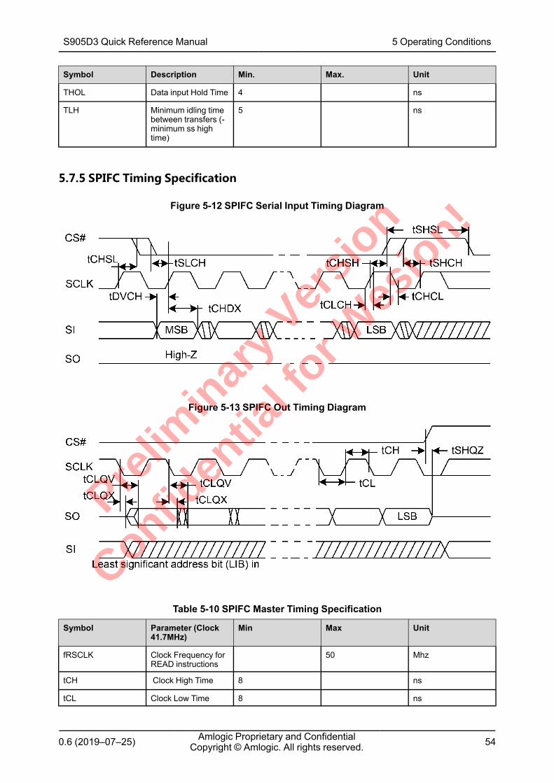
0.6 (2019–07–25) Amlogic Proprietary and ConfidentialCopyright © Amlogic. All rights reserved. 54
Symbol Description Min. Max. Unit
THOL Data input Hold Time 4 ns
TLH Minimum idling timebetween transfers (-minimum ss hightime)
5 ns
5.7.5 SPIFC Timing Specification
Figure 5-12 SPIFC Serial Input Timing Diagram
Figure 5-13 SPIFC Out Timing Diagram
Table 5-10 SPIFC Master Timing Specification
Symbol Parameter (Clock41.7MHz)
Min Max Unit
fRSCLK Clock Frequency forREAD instructions
50 Mhz
tCH Clock High Time 8 ns
tCL Clock Low Time 8 ns
S905D3 Quick Reference Manual 5 Operating Conditions
Prelim
inar
y Ver
sion
Confiden
tial f
or Wes
ion!
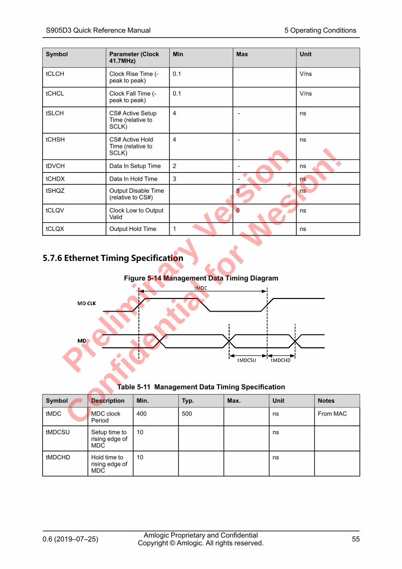
0.6 (2019–07–25) Amlogic Proprietary and ConfidentialCopyright © Amlogic. All rights reserved. 55
Symbol Parameter (Clock41.7MHz)
Min Max Unit
tCLCH Clock Rise Time (-peak to peak)
0.1 V/ns
tCHCL Clock Fall Time (-peak to peak)
0.1 V/ns
tSLCH CS# Active SetupTime (relative toSCLK)
4 - ns
tCHSH CS# Active HoldTime (relative toSCLK)
4 - ns
tDVCH Data In Setup Time 2 - ns
tCHDX Data In Hold Time 3 - ns
tSHQZ Output Disable Time(relative to CS#)
8 ns
tCLQV Clock Low to OutputValid
6 ns
tCLQX Output Hold Time 1 ns
5.7.6 Ethernet Timing Specification
Figure 5-14 Management Data Timing Diagram
Table 5-11 Management Data Timing Specification
Symbol Description Min. Typ. Max. Unit Notes
tMDC MDC clockPeriod
400 500 ns From MAC
tMDCSU Setup time torising edge ofMDC
10 ns
tMDCHD Hold time torising edge ofMDC
10 ns
S905D3 Quick Reference Manual 5 Operating Conditions
Prelim
inar
y Ver
sion
Confiden
tial f
or Wes
ion!
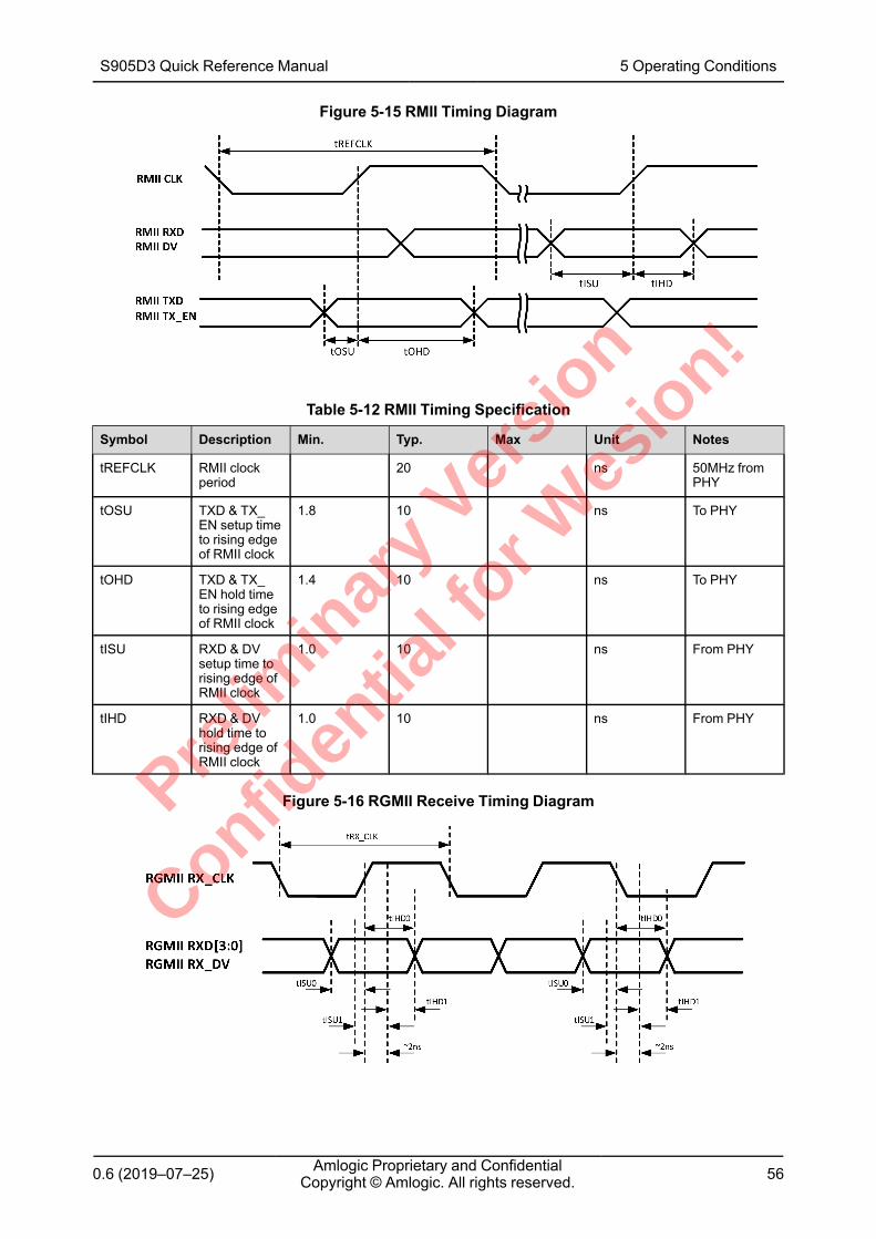
0.6 (2019–07–25) Amlogic Proprietary and ConfidentialCopyright © Amlogic. All rights reserved. 56
Figure 5-15 RMII Timing Diagram
Table 5-12 RMII Timing Specification
Symbol Description Min. Typ. Max Unit Notes
tREFCLK RMII clockperiod
20 ns 50MHz fromPHY
tOSU TXD & TX_EN setup timeto rising edgeof RMII clock
1.8 10 ns To PHY
tOHD TXD & TX_EN hold timeto rising edgeof RMII clock
1.4 10 ns To PHY
tISU RXD & DVsetup time torising edge ofRMII clock
1.0 10 ns From PHY
tIHD RXD & DVhold time torising edge ofRMII clock
1.0 10 ns From PHY
Figure 5-16 RGMII Receive Timing Diagram
S905D3 Quick Reference Manual 5 Operating Conditions
Prelim
inar
y Ver
sion
Confiden
tial f
or Wes
ion!
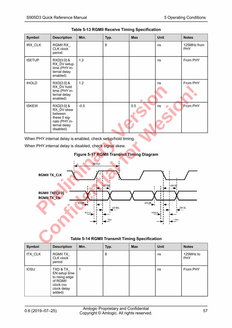
0.6 (2019–07–25) Amlogic Proprietary and ConfidentialCopyright © Amlogic. All rights reserved. 57
Table 5-13 RGMII Receive Timing Specification
Symbol Description Min. Typ. Max Unit Notes
tRX_CLK RGMII RX_CLK clockperiod
8 ns 125MHz fromPHY
tSETUP RXD[3:0] &RX_DV setuptime (PHY in-ternal delayenabled)
1.2 ns From PHY
tHOLD RXD[3:0] &RX_DV holdtime (PHY in-ternal delayenabled)
1.2 ns From PHY
tSKEW RXD[3:0] &RX_DV skewbetweenthese 5 sig-nals (PHY in-ternal delaydisabled)
-0.5 0.5 ns From PHY
When PHY internal delay is enabled, check setup/hold timing.
When PHY internal delay is disabled, check signal skew.
Figure 5-17 RGMII Transmit Timing Diagram
Table 5-14 RGMII Transmit Timing Specification
Symbol Description Min. Typ. Max Unit Notes
tTX_CLK RGMII TX_CLK clockperiod
8 ns 125MHz toPHY
tOSU TXD & TX_EN setup timeto rising edgeof RGMIIclock (noclock delayadded)
1 ns From PHY
S905D3 Quick Reference Manual 5 Operating Conditions
Prelim
inar
y Ver
sion
Confiden
tial f
or Wes
ion!
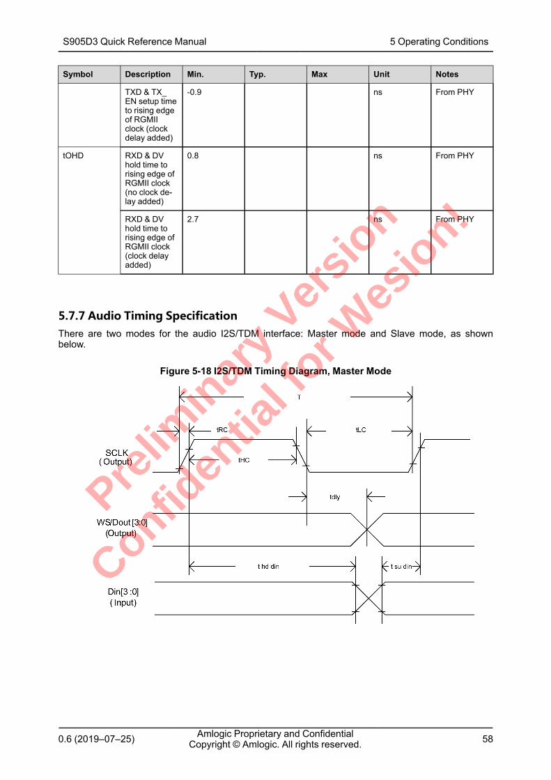
0.6 (2019–07–25) Amlogic Proprietary and ConfidentialCopyright © Amlogic. All rights reserved. 58
Symbol Description Min. Typ. Max Unit Notes
TXD & TX_EN setup timeto rising edgeof RGMIIclock (clockdelay added)
-0.9 ns From PHY
tOHD RXD & DVhold time torising edge ofRGMII clock(no clock de-lay added)
0.8 ns From PHY
RXD & DVhold time torising edge ofRGMII clock(clock delayadded)
2.7 ns From PHY
5.7.7 Audio Timing SpecificationThere are two modes for the audio I2S/TDM interface: Master mode and Slave mode, as shownbelow.
Figure 5-18 I2S/TDM Timing Diagram, Master Mode
S905D3 Quick Reference Manual 5 Operating Conditions
Prelim
inar
y Ver
sion
Confiden
tial f
or Wes
ion!
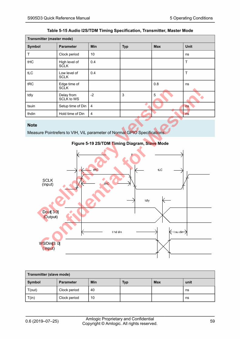
0.6 (2019–07–25) Amlogic Proprietary and ConfidentialCopyright © Amlogic. All rights reserved. 59
Table 5-15 Audio I2S/TDM Timing Specification, Transmitter, Master Mode
Transmitter (master mode)
Symbol Parameter Min Typ Max Unit
T Clock period 10 ns
tHC High level ofSCLK
0.4 T
tLC Low level ofSCLK
0.4 T
tRC Edge time ofSCLK
0.8 ns
tdly Delay fromSCLK to WS
-2 3 5
tsuin Setup time of Din 4 ns
thdin Hold time of Din 4 ns
NoteMeasure Pointrefers to VIH, ViL parameter of Normal GPIO Specifications.
Figure 5-19 2S/TDM Timing Diagram, Slave Mode
Transmitter (slave mode)
Symbol Parameter Min Typ Max unit
T(out) Clock period 40 ns
T(in) Clock period 10 ns
S905D3 Quick Reference Manual 5 Operating Conditions
Prelim
inar
y Ver
sion
Confiden
tial f
or Wes
ion!
0.6 (2019–07–25) Amlogic Proprietary and ConfidentialCopyright © Amlogic. All rights reserved. 60
Transmitter (slave mode)
Symbol Parameter Min Typ Max unit
tHC High level ofSCLK
0.4 T
tLC Low level ofSCLK
0.4 T
tRC Edge time ofSCLK
0.8 ns
tsu in Setup time ofWS/Din
4 ns
thd in Hold time of WS/Din
4 ns
tdly Delay betweenSCLK and Dout
2 12 15 ns
NoteMeasure Pointrefers to VIH, ViL parameter of Normal GPIO Specifications.
S905D3 Quick Reference Manual 5 Operating Conditions
Prelim
inar
y Ver
sion
Confiden
tial f
or Wes
ion!
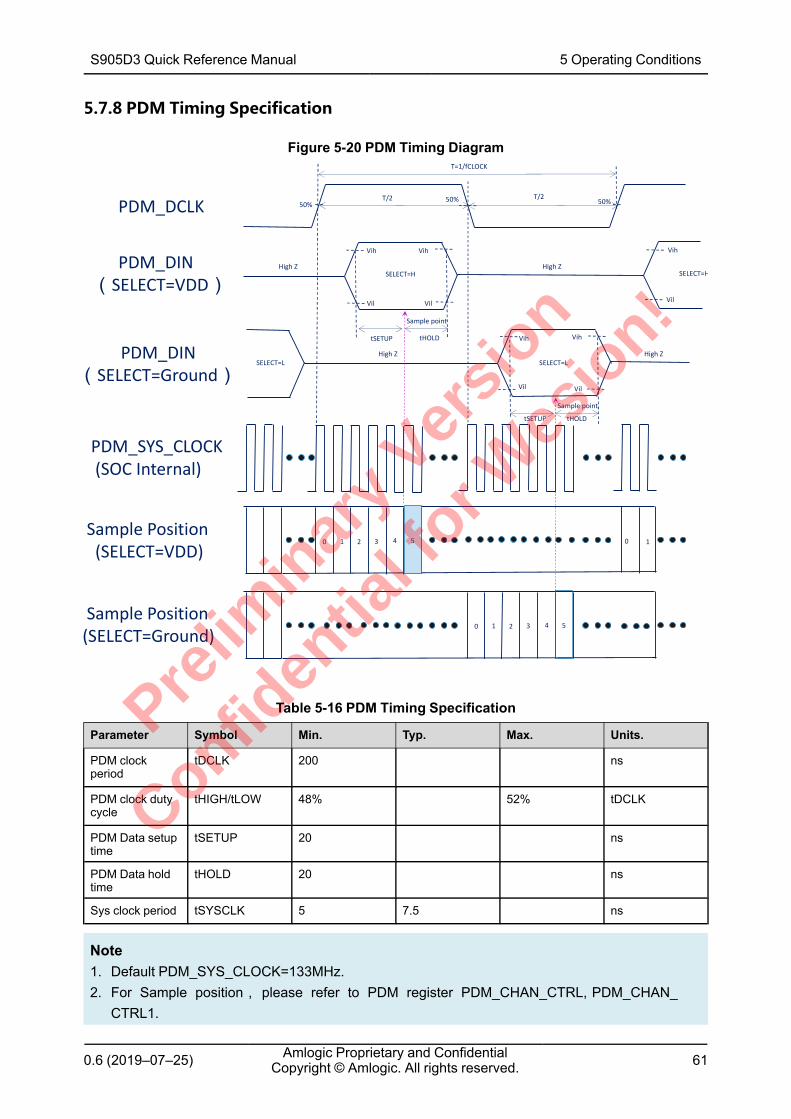
0.6 (2019–07–25) Amlogic Proprietary and ConfidentialCopyright © Amlogic. All rights reserved. 61
5.7.8 PDM Timing Specification
Figure 5-20 PDM Timing Diagram
Table 5-16 PDM Timing Specification
Parameter Symbol Min. Typ. Max. Units.
PDM clockperiod
tDCLK 200 ns
PDM clock dutycycle
tHIGH/tLOW 48% 52% tDCLK
PDM Data setuptime
tSETUP 20 ns
PDM Data holdtime
tHOLD 20 ns
Sys clock period tSYSCLK 5 7.5 ns
Note1. Default PDM_SYS_CLOCK=133MHz.2. For Sample position, please refer to PDM register PDM_CHAN_CTRL, PDM_CHAN_
CTRL1.
SELECT=H
SELECT=L
SELECT=H
T=1/fCLOCK
50%50% 50%T/2 T/2
Vih
Vil
Vih
Vil
Vil
Vih
High Z High Z
High ZSELECT=L
High Z
PDM_DCLK
PDM_DIN(SELECT=VDD)
PDM_DIN(SELECT=Ground)
0 1
Sample point
Sample point
PDM_SYS_CLOCK(SOC Internal)
Sample Position(SELECT=VDD)
0 1 2 3 4 5
Vih
Vil
tSETUP
tSETUP tHOLD
tHOLD
Vih
Vil
0 1 2 3 4 5Sample Position
(SELECT=Ground)
S905D3 Quick Reference Manual 5 Operating Conditions
Prelim
inar
y Ver
sion
Confiden
tial f
or Wes
ion!
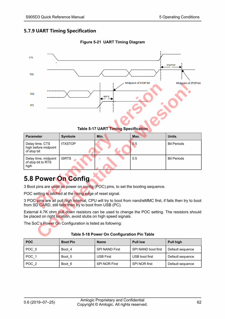
0.6 (2019–07–25) Amlogic Proprietary and ConfidentialCopyright © Amlogic. All rights reserved. 62
5.7.9 UART Timing Specification
Figure 5-21 UART Timing Diagram
Table 5-17 UART Timing Specification
Parameter Symbole Min. Max. Units.
Delay time, CTShigh before midpointof stop bit
tTXSTOP - 0.5 Bit Periods
Delay time, midpointof stop bit to RTShgih
tSRTS - 0.5 Bit Periods
5.8 Power On Config3 Boot pins are used as power on config (POC) pins, to set the booting sequence.
POC setting is latched at the rising edge of reset signal.
3 POC pins are all pull high internal, CPU will try to boot from nand/eMMC first, if fails then try to bootfrom SD CARD, still fails then try to boot from USB (PC).
External 4.7K ohm pull down resistors can be used to change the POC setting. The resistors shouldbe placed on right location, avoid stubs on high speed signals.
The SoC’s Power On Configuration is listed as following:
Table 5-18 Power On Configuration Pin Table
POC Boot Pin Name Pull low Pull high
POC_0 Boot_4 SPI NAND First SPI NAND boot first Default sequence
POC_1 Boot_5 USB First USB boot first Default sequence
POC_2 Boot_6 SPI NOR First SPI NOR first Default sequence
S905D3 Quick Reference Manual 5 Operating Conditions
Prelim
inar
y Ver
sion
Confiden
tial f
or Wes
ion!
0.6 (2019–07–25) Amlogic Proprietary and ConfidentialCopyright © Amlogic. All rights reserved. 63
Table 5-19 Booting Sequence Diagram
No. POC_0(SPI_NAND)
POC_1(USB_BOOT)
POC_2(SPI_NOR,eMMC/NAND )
1st Bootdevice
2nd Bootdevice
3rd Bootdevice
4th Bootdevice
1 0 0 0 USB (shortdelay)
SPI_NOR NAND/eMMC
SD Card
2 0 0 1 USB (shortdelay)
NAND/eMMC
SD Card -
3 0 1 0 SPI_NOR NAND/eMMC
SD Card USB
4 0 1 1 SPI_NAND NAND/eMMC
USB -
5 1 0 0 USB (shortdelay)
SPI_NOR NAND/eMMC
SD Card
6 1 0 1 USB (shortdelay)
NAND/eMMC
SD Card -
7 1 1 0 SPI_NOR NAND/eMMC
SD Card USB
8 1 1 1 NAND/eMMC
SD Card USB -
NoteIf GPIOC is not work as SDIO port, please do not pull CARD_DET(GPIOC_6) low when systembooting up, to avoid romcode trying to boot from SD CARD.
5.9 Power On ResetThe POR (Power On Reset) monitors VDDIO_AO power voltage and compares it to a thresholdVoltage.
RESET_N pin is low (SOC is reset mode) when VDDIO_AO is below threshold,
Force SOC enter reset mode via key to GND serial 100R resitor.
Note1. Place 1nF capacitors on RESET_N Pin.2. VDDIO_AO power pin is only support 3.3V,not allow to power off in sleep mode.
S905D3 Quick Reference Manual 5 Operating Conditions
Prelim
inar
y Ver
sion
Confiden
tial f
or Wes
ion!
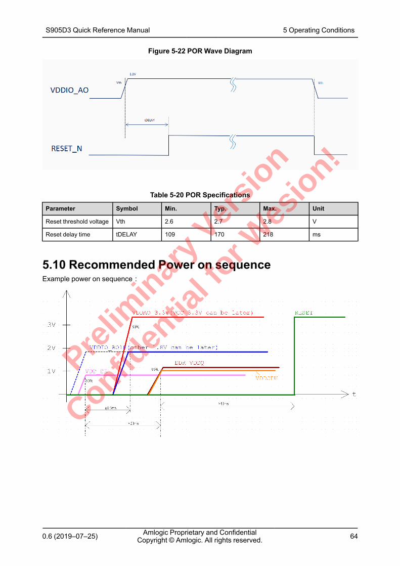
0.6 (2019–07–25) Amlogic Proprietary and ConfidentialCopyright © Amlogic. All rights reserved. 64
Figure 5-22 PORWave Diagram
Table 5-20 POR Specifications
Parameter Symbol Min. Typ. Max. Unit
Reset threshold voltage Vth 2.6 2.7 2.8 V
Reset delay time tDELAY 109 170 218 ms
5.10 Recommended Power on sequenceExample power on sequence:
S905D3 Quick Reference Manual 5 Operating Conditions
Prelim
inar
y Ver
sion
Confiden
tial f
or Wes
ion!
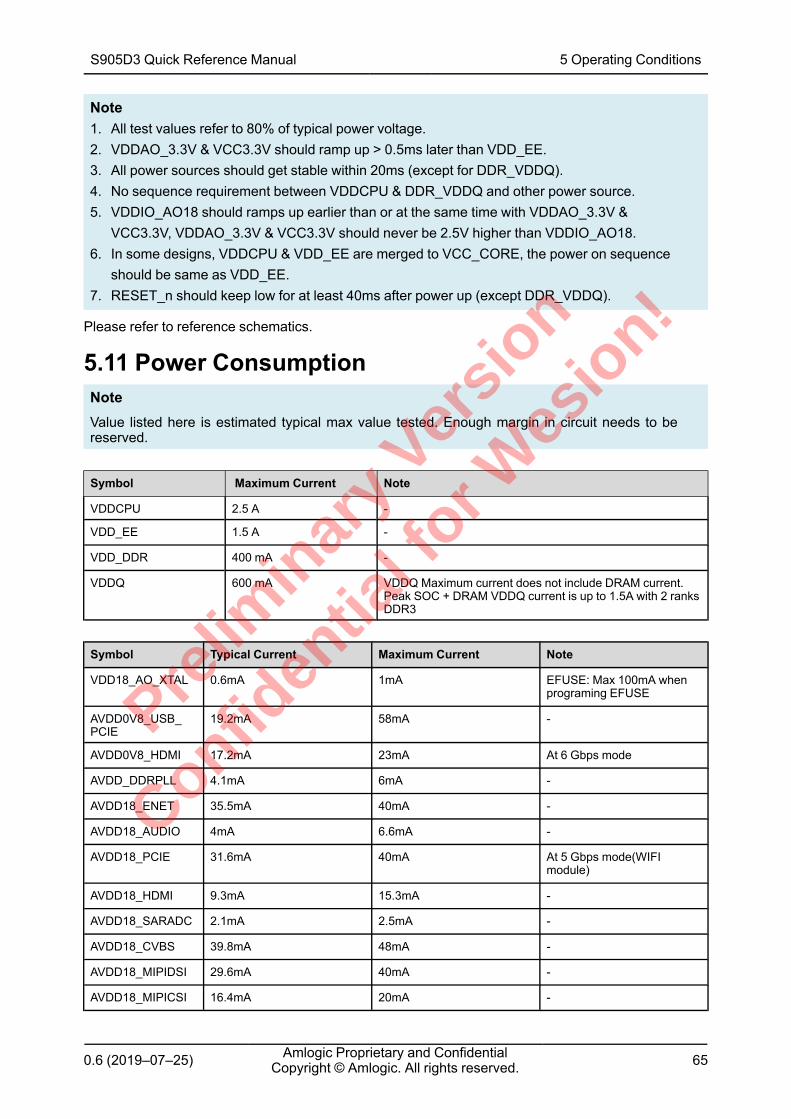
0.6 (2019–07–25) Amlogic Proprietary and ConfidentialCopyright © Amlogic. All rights reserved. 65
Note1. All test values refer to 80% of typical power voltage.2. VDDAO_3.3V & VCC3.3V should ramp up > 0.5ms later than VDD_EE.3. All power sources should get stable within 20ms (except for DDR_VDDQ).4. No sequence requirement between VDDCPU & DDR_VDDQ and other power source.5. VDDIO_AO18 should ramps up earlier than or at the same time with VDDAO_3.3V &
VCC3.3V, VDDAO_3.3V & VCC3.3V should never be 2.5V higher than VDDIO_AO18.6. In some designs, VDDCPU & VDD_EE are merged to VCC_CORE, the power on sequence
should be same as VDD_EE.7. RESET_n should keep low for at least 40ms after power up (except DDR_VDDQ).
Please refer to reference schematics.
5.11 Power ConsumptionNoteValue listed here is estimated typical max value tested. Enough margin in circuit needs to bereserved.
Symbol Maximum Current Note
VDDCPU 2.5 A -
VDD_EE 1.5 A -
VDD_DDR 400 mA -
VDDQ 600 mA VDDQ Maximum current does not include DRAM current.Peak SOC + DRAM VDDQ current is up to 1.5A with 2 ranksDDR3
Symbol Typical Current Maximum Current Note
VDD18_AO_XTAL 0.6mA 1mA EFUSE: Max 100mA whenprograming EFUSE
AVDD0V8_USB_PCIE
19.2mA 58mA -
AVDD0V8_HDMI 17.2mA 23mA At 6 Gbps mode
AVDD_DDRPLL 4.1mA 6mA -
AVDD18_ENET 35.5mA 40mA -
AVDD18_AUDIO 4mA 6.6mA -
AVDD18_PCIE 31.6mA 40mA At 5 Gbps mode(WIFImodule)
AVDD18_HDMI 9.3mA 15.3mA -
AVDD18_SARADC 2.1mA 2.5mA -
AVDD18_CVBS 39.8mA 48mA -
AVDD18_MIPIDSI 29.6mA 40mA -
AVDD18_MIPICSI 16.4mA 20mA -
S905D3 Quick Reference Manual 5 Operating Conditions
Prelim
inar
y Ver
sion
Confiden
tial f
or Wes
ion!
0.6 (2019–07–25) Amlogic Proprietary and ConfidentialCopyright © Amlogic. All rights reserved. 66
Symbol Typical Current Maximum Current Note
AVDD18_USB 18.2mA 25mA -
AVDD33_USB 0.3mA 2mA -
AVDD18_DPLL 23.2mA 25mA -
VDDIO Note
NoteVDDIO=1.8V, DS=3, output 200MHz clock:1. IO pad itself consumes about 1.4mA.2. Driving a 55ohm trace with length of 50mm and width of 0.1mm will consumes about 2.8mA
additional current (low impedance trace consumes more power)3. Base on #2, add 5pF cap will consumes about 1.8mA additional current, total about 6mA4. When VDDIO=3.3V, GPIO consumes about 70% higher current,about 13mA.5. Internal & external pull down resistor consumes more current.
5.12 Storage and Baking ConditionsThe processor is moisture-sensitive device of MSL level 3, defined by IPC/JEDEC J-STD-020. Pleasefollow the storage and backing guidelines.
1. Calculated shelf life in sealed bag: 12 months at <40°C and <90% relative humidity (RH).2. After bag is opened, devices that will be subjected to reflow solder or other high temperature
process must be
a. Mounted with 168 hours of factory conditions ≤30°C/60% RH, orb. Stored per J-STD-033
3. Devices require bake, before mounting, if Humidity Indicator Card reads >10%.4. If baking is required, refer IPC/JEDEC J-STB-033 for baking process.
S905D3 Quick Reference Manual 5 Operating Conditions
Prelim
inar
y Ver
sion
Confiden
tial f
or Wes
ion!
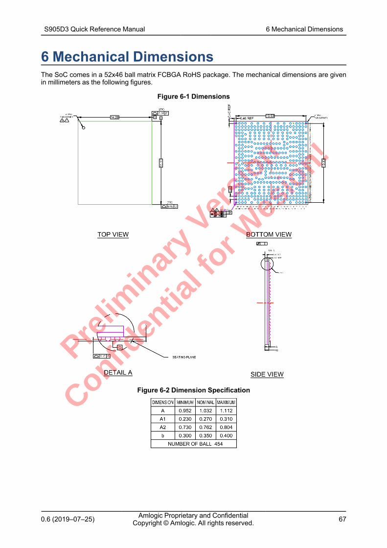
0.6 (2019–07–25) Amlogic Proprietary and ConfidentialCopyright © Amlogic. All rights reserved. 67
6 Mechanical DimensionsThe SoC comes in a 52x46 ball matrix FCBGA RoHS package. The mechanical dimensions are givenin millimeters as the following figures.
Figure 6-1 Dimensions
Figure 6-2 Dimension Specification
S905D3 Quick Reference Manual 6 Mechanical Dimensions
Prelim
inar
y Ver
sion
Confiden
tial f
or Wes
ion!