Embed Size (px)
Citation preview

8/14/2019 Sematech_FEOL_Challenges.pdf
http://slidepdf.com/reader/full/sematechfeolchallengespdf 1/34
April 15, 2008
MODERATOR:
Aaron HandExecutive Editor,Electronic MediaSemiconductor International

8/14/2019 Sematech_FEOL_Challenges.pdf
http://slidepdf.com/reader/full/sematechfeolchallengespdf 2/34
Ultra-high purity chemical pumps, mixers, and liquid heaters
www.idex-hs.com

8/14/2019 Sematech_FEOL_Challenges.pdf
http://slidepdf.com/reader/full/sematechfeolchallengespdf 3/34
April 15, 2008
MODERATOR:
Aaron HandExecutive Editor,Electronic MediaSemiconductor International

8/14/2019 Sematech_FEOL_Challenges.pdf
http://slidepdf.com/reader/full/sematechfeolchallengespdf 4/34
Webcast: Wafer Cleaning Solutions for 45 and 32 nm,Semiconductor International , 4/15/2008
Panelists
D. Martin Knotter
Senior Principal Scientist
Contamination Expertise CenterNXP Semiconductors
Jeffrey Butterbaugh
Chairman, ITRS Front End Processes TWG
Chief Technologist
FSI International
Anthony Muscat
Associate Professor
Department of Chemical & Environmental EngineeringUniversity of Arizona
Brian Kirkpatrick
Senior Member of Technical Staff
Texas Instruments

8/14/2019 Sematech_FEOL_Challenges.pdf
http://slidepdf.com/reader/full/sematechfeolchallengespdf 5/34
Webcast: Wafer Cleaning Solutions for 45 and 32 nm,Semiconductor International , 4/15/2008
A View of The ChallengesFrom the 2007 ITRS
Jeffery W. ButterbaughFSI International
3455 Lyman Boulevard
Chaska, Minnesota 55347 USA
phone: 952-448-8089
e-mail: [email protected]

8/14/2019 Sematech_FEOL_Challenges.pdf
http://slidepdf.com/reader/full/sematechfeolchallengespdf 6/34
Webcast: Wafer Cleaning Solutions for 45 and 32 nm,Semiconductor International , 4/15/2008
The “Crux” of the Scaling Problem. . . . traditional transistor and capacitor formation materials, silicon,
silicon dioxide, and polysilicon have been pushed to fundamentalmaterial limits and continued scaling has required the introduction ofnew materials. The current situation can be defined as “material-limited device scaling.” In addition, new approaches to devicestructure, such as non-planar multi-gate devices, will be needed forfuture performance scaling. . . .

8/14/2019 Sematech_FEOL_Challenges.pdf
http://slidepdf.com/reader/full/sematechfeolchallengespdf 7/34Webcast: Wafer Cleaning Solutions for 45 and 32 nm,Semiconductor International , 4/15/2008
“More than Moore”
8/14/2019 Sematech_FEOL_Challenges.pdf
http://slidepdf.com/reader/full/sematechfeolchallengespdf 8/34Webcast: Wafer Cleaning Solutions for 45 and 32 nm,Semiconductor International , 4/15/2008
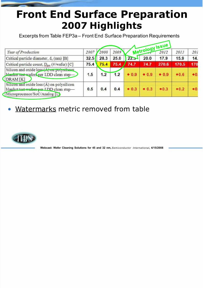
Front End Surface Preparation2007 Highlights
Excerpts from Table FEP3a – Front End Surface Preparation Requirements
• Watermarks metric removed from table

8/14/2019 Sematech_FEOL_Challenges.pdf
http://slidepdf.com/reader/full/sematechfeolchallengespdf 9/34Webcast: Wafer Cleaning Solutions for 45 and 32 nm,Semiconductor International , 4/15/2008
Thermal/Thin Films/Doping
2008
2010
2011

8/14/2019 Sematech_FEOL_Challenges.pdf
http://slidepdf.com/reader/full/sematechfeolchallengespdf 10/34Webcast: Wafer Cleaning Solutions for 45 and 32 nm,Semiconductor International , 4/15/2008
Etch2007 Highlights
• Atomic Layer Etching adding to potential solutions table
Excerpts from Table FEP4a – Thermal/Thin Films/Doping/Etch Requirements

8/14/2019 Sematech_FEOL_Challenges.pdf
http://slidepdf.com/reader/full/sematechfeolchallengespdf 11/34Webcast: Wafer Cleaning Solutions for 45 and 32 nm,Semiconductor International , 4/15/2008
Stacked DRAM2007 Highlights
Excerpts from Table FEP5a – DRAM Stacked Capacitor Requirements
Excerpts from Figure FEP7 – DRAM Stacked Capacitor Potential Solutions

8/14/2019 Sematech_FEOL_Challenges.pdf
http://slidepdf.com/reader/full/sematechfeolchallengespdf 12/34Webcast: Wafer Cleaning Solutions for 45 and 32 nm,Semiconductor International , 4/15/2008
Flash2007 Highlights
Excerpts from Table FEP7 – Flash Requirements

8/14/2019 Sematech_FEOL_Challenges.pdf
http://slidepdf.com/reader/full/sematechfeolchallengespdf 13/34Webcast: Wafer Cleaning Solutions for 45 and 32 nm,Semiconductor International , 4/15/2008
Perspective on Front End of LineWafer Cleaning Solutions for 45 and 32 nm
Anthony Muscat
Department of Chemical and Environmental EngineeringUniversity of Arizona, Tucson, AZ 85721

8/14/2019 Sematech_FEOL_Challenges.pdf
http://slidepdf.com/reader/full/sematechfeolchallengespdf 14/34Webcast: Wafer Cleaning Solutions for 45 and 32 nm,Semiconductor International , 4/15/2008
Novel Materials and Device Issues
• Fermi level pinning
• Cleaning multicomponent substrates
–Passivate and tie up dangling bonds
• Closer integration of surface preparationwith deposition

8/14/2019 Sematech_FEOL_Challenges.pdf
http://slidepdf.com/reader/full/sematechfeolchallengespdf 15/34Webcast: Wafer Cleaning Solutions for 45 and 32 nm,Semiconductor International , 4/15/2008
Fermi Level Pinning at Critical Interfaces
Passlack et al., IEEE Electron Device Letters 23(9) (2002) 508.
• Electronic states in the bandgap atAlGaAs/Ga2O3 interface full of electrons,which pins Fermi level in depletion
mode devices– O at interface pins III-V materials
• Causes of Fermi level pinning/unpinningat oxide/III-V interfaces not well
understood

8/14/2019 Sematech_FEOL_Challenges.pdf
http://slidepdf.com/reader/full/sematechfeolchallengespdf 16/34Webcast: Wafer Cleaning Solutions for 45 and 32 nm,Semiconductor International , 4/15/2008
• Liquid phase HF on InAs(100)– Removed In2O3 and As2O5
– As-rich bulk metal and overlayer contained As2O3 but notAs-F
– As atoms could be responsible for Fermi level pinning
Cleaning Multicomponent Substrates: InAs

8/14/2019 Sematech_FEOL_Challenges.pdf
http://slidepdf.com/reader/full/sematechfeolchallengespdf 17/34
Webcast: Wafer Cleaning Solutions for 45 and 32 nm,Semiconductor International , 4/15/2008
• Liquid phase HF on InSb(100)– Removed In2O3 and Sb2O5
– Sb-rich overlayer contained Sb-F
– Bulk InSb stoichiometric
Cleaning Multicomponent Substrates: InSb

8/14/2019 Sematech_FEOL_Challenges.pdf
http://slidepdf.com/reader/full/sematechfeolchallengespdf 18/34
Webcast: Wafer Cleaning Solutions for 45 and 32 nm,Semiconductor International , 4/15/2008
Integrated Clean and Deposition: Al2O3 on InSb
• Interfacial reaction between surface speciesand ALD precursors– Reacted In2O3 and InF3
– Reacted elemental As and AsF3 to As2O5 and As2O3
– Large driving force to form bonds with Al
8/14/2019 Sematech_FEOL_Challenges.pdf
http://slidepdf.com/reader/full/sematechfeolchallengespdf 19/34
Webcast: Wafer Cleaning Solutions for 45 and 32 nm,Semiconductor International , 4/15/2008
Wafer Environment ControlChallenges for 32 and 45 nm technology
Martin Knotter
Impact determinationMEDEA+ 2T102 “HYMNE” WP3.1
April, 02, 2008

8/14/2019 Sematech_FEOL_Challenges.pdf
http://slidepdf.com/reader/full/sematechfeolchallengespdf 20/34
Webcast: Wafer Cleaning Solutions for 45 and 32 nm,Semiconductor International , 4/15/2008
Challenge Is: “What Do We Really Need?”
Specification in Wafer Environment andSurface Contamination are based on(order of occurrence):
1. Best available on the market (supplier driven,sometimes because customer X asks)
2. Extrapolations from the past
3. Short loops
4. Fab X, with unknown contamination finger printand fudge kill ratios

8/14/2019 Sematech_FEOL_Challenges.pdf
http://slidepdf.com/reader/full/sematechfeolchallengespdf 21/34
Webcast: Wafer Cleaning Solutions for 45 and 32 nm,Semiconductor International , 4/15/2008
Do We Understand Failure Path?
Contaminant
in water/air Contaminant on wafer
Where?
How?
When?
How?
Failing dies
It is not easy to use controlled contamination in awafer fab for impact determination statistics of
noise of unknown origin

8/14/2019 Sematech_FEOL_Challenges.pdf
http://slidepdf.com/reader/full/sematechfeolchallengespdf 22/34
Webcast: Wafer Cleaning Solutions for 45 and 32 nm,Semiconductor International , 4/15/2008
HYMNE Work Package 3.1Impact Determination
High Yield driven MaNufacturing
Excellence in sub 65 nm CMOS
is a European Project
Partners in WP3.1:

8/14/2019 Sematech_FEOL_Challenges.pdf
http://slidepdf.com/reader/full/sematechfeolchallengespdf 23/34
Webcast: Wafer Cleaning Solutions for 45 and 32 nm,Semiconductor International , 4/15/2008
NEW Work in Progress:Non-uniform Contamination
3.1.1. Controlled contamination3.1.2. Short Loops (see Adrien Danel Surface PotentialMeasurements)3.1.3. Kill ratio analysis (see Faisal Wali: particles in Fab X)3.1.4. Deposition Probability (see Y. Borde: metalcontamination through solid contacts)
Uniform distribution is the spec (partly because ofanalytical limitation)
Do we have a serious analytical issue?

8/14/2019 Sematech_FEOL_Challenges.pdf
http://slidepdf.com/reader/full/sematechfeolchallengespdf 24/34
Webcast: Wafer Cleaning Solutions for 45 and 32 nm,Semiconductor International , 4/15/2008
NXP Contribution
Impact of random contamination is bestdetermined in mature fabs
NXP turns into automotive and already
finds impact in their 350-nm products
Automotive and not advanced CMOS isthe driver for contaminationspecifications?

8/14/2019 Sematech_FEOL_Challenges.pdf
http://slidepdf.com/reader/full/sematechfeolchallengespdf 25/34
Webcast: Wafer Cleaning Solutions for 45 and 32 nm,Semiconductor International , 4/15/2008
Summary of Statements
1. The contamination roadmap is supplierdriven, while IC manufacturer should tellthe supplier what he needs (based on facts)
2. We have an analytical problem forquantification of non-uniform contamination
3. Automotive requirements should drive thecontamination roadmap

8/14/2019 Sematech_FEOL_Challenges.pdf
http://slidepdf.com/reader/full/sematechfeolchallengespdf 26/34
Webcast: Wafer Cleaning Solutions for 45 and 32 nm,Semiconductor International , 4/15/2008
Front End of Line Wafer CleaningSolutions for 45 and 32 nm
Brian KirkpatrickExternal Development and Manufacturing
Texas Instruments

8/14/2019 Sematech_FEOL_Challenges.pdf
http://slidepdf.com/reader/full/sematechfeolchallengespdf 27/34
Webcast: Wafer Cleaning Solutions for 45 and 32 nm,Semiconductor International , 4/15/2008
Surface Preparation Impact onDevice Performance
• Energy conservation– Economics• It’s not just gasoline• Ioff as important as Ion
– Which devices
• Not just battery operated– Increasing consequences
• Heat dissipation• Reliability• Battery life
• Average device packing density will diverge fromMoore’s Law unless Jg held constant with decreasingToxinv
– Macro level problems• Cooling server farms
8/14/2019 Sematech_FEOL_Challenges.pdf
http://slidepdf.com/reader/full/sematechfeolchallengespdf 28/34
Webcast: Wafer Cleaning Solutions for 45 and 32 nm,Semiconductor International , 4/15/2008
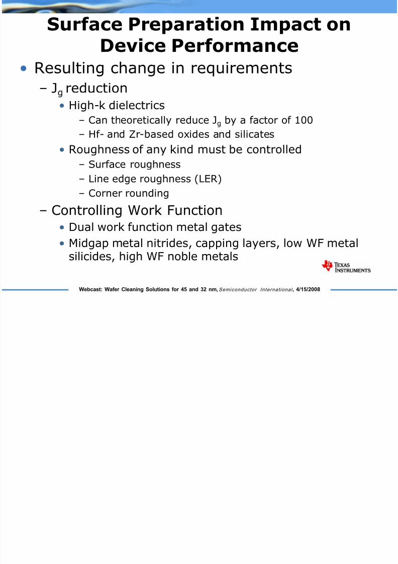
Surface Preparation Impact onDevice Performance
• Resulting change in requirements– Jg reduction
• High-k dielectrics
– Can theoretically reduce Jg by a factor of 100
– Hf- and Zr-based oxides and silicates
• Roughness of any kind must be controlled
– Surface roughness
– Line edge roughness (LER)
– Corner rounding
– Controlling Work Function• Dual work function metal gates
• Midgap metal nitrides, capping layers, low WF metalsilicides, high WF noble metals

8/14/2019 Sematech_FEOL_Challenges.pdf
http://slidepdf.com/reader/full/sematechfeolchallengespdf 29/34
Webcast: Wafer Cleaning Solutions for 45 and 32 nm,Semiconductor International , 4/15/2008
Surface Preparation Impact onDevice Performance
– Cross-contamination concerns for high-k /metal gates
• Restricting tool usage
• Backside cleans to allow some sharing (metrology,
photolithography, … not high temperature)
• Rigorous testing methods
8/14/2019 Sematech_FEOL_Challenges.pdf
http://slidepdf.com/reader/full/sematechfeolchallengespdf 30/34
Webcast: Wafer Cleaning Solutions for 45 and 32 nm,Semiconductor International , 4/15/2008
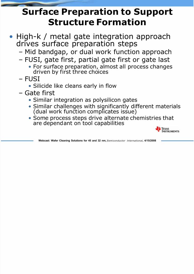
Surface Preparation to SupportStructure Formation
• High-k / metal gate integration approachdrives surface preparation steps– Mid bandgap, or dual work function approach– FUSI, gate first, partial gate first or gate last
• For surface preparation, almost all process changesdriven by first three choices
– FUSI• Silicide like cleans early in flow
– Gate first
• Similar integration as polysilicon gates• Similar challenges with significantly different materials(dual work function complicates issue)
• Some process steps drive alternate chemistries thatare dependant on tool capabilities

8/14/2019 Sematech_FEOL_Challenges.pdf
http://slidepdf.com/reader/full/sematechfeolchallengespdf 31/34
Webcast: Wafer Cleaning Solutions for 45 and 32 nm,Semiconductor International , 4/15/2008
Surface Preparation to SupportStructure Formation
– Example; Post gate etch clean» Brief exposure to concentrated chemistry ideal. If
brief exposure not possible, then achieve requiredcleaning capability and etch selectivity by movingto higher temperatures with the buffers to modifypH.
– Partial gate first• Wet processes being used to remove the replacement
gate electrode– High-k material exposed during wet etch
» Extreme selectivity requirement
– Sidewalls and LDD implants may already be in place– Post CMP clean involving metals required around the
gate process step

8/14/2019 Sematech_FEOL_Challenges.pdf
http://slidepdf.com/reader/full/sematechfeolchallengespdf 32/34
Webcast: Wafer Cleaning Solutions for 45 and 32 nm,Semiconductor International , 4/15/2008
Surface Preparation to SupportStructure Formation
• Managing material consumption– Not just silicon (see separate presentation)• Isolation Loop = Active silicon• Gate Loop = Silicon recess• USJ Loop = Sidewall loss, silicon recess
• SiGe Loop = Sidewall loss, silicon recess profile and depthcontrol• Contact = Sidewall profile, silicide consumption
– Eliminating unnecessary cleans (again)– Optimizing and minimizing photo reworks
– Process changes• Increased use of single wafer tools• Paradigm shift
– FEOL; Less ash All wet– BEOL; Insitu ash (within plasma etch tools) External process

8/14/2019 Sematech_FEOL_Challenges.pdf
http://slidepdf.com/reader/full/sematechfeolchallengespdf 33/34
Webcast: Wafer Cleaning Solutions for 45 and 32 nm,Semiconductor International , 4/15/2008
Surface Preparation to SupportStructure Formation
• Through-silicon vias (TSVs)– Advanced interconnect method
• Post-etch cleans with huge, deep trenches exposed
• Dependant on integration, micro-machining like stepsmay be required
• TSVs require post-CMP clean on very thin wafers
– Wafer carriers
– Need to completely remove damaged layer
• MuGFETs
• High-mobility channels– Ge, III-V compounds (GaAs) on horizon
– Carbon nanotubes, graphenes, InAs and InSbstarting to be discussed

8/14/2019 Sematech_FEOL_Challenges.pdf
http://slidepdf.com/reader/full/sematechfeolchallengespdf 34/34
Panelists
D. Martin Knotter
Senior Principal Scientist
Contamination Expertise CenterNXP Semiconductors
Jeffrey Butterbaugh
Chairman, ITRS Front End Processes TWG
Chief Technologist
FSI International
Anthony Muscat
Associate Professor
Department of Chemical & Environmental EngineeringUniversity of Arizona
Brian Kirkpatrick
Senior Member of Technical Staff
Texas Instruments


