Embed Size (px)
Citation preview
Seperation of semiconductor layers from thin film solar panels using microwave radiation
Proceedings of EMC 2015 1
Separation of semiconductor layers from thin film
solar panels using microwave radiation
Dipl.-Ing. M Bartosinski, D. Michaelis M.Sc., Prof. Dr-Ing. Dr. h.c. B Friedrich
IME Process Metallurgy and Metal Recycling
Intzestraße 3
52072 Aachen, Germany
Abstract
Being the two most promising thin film solar cells, the production of Cadmium Telluride (CdTe)-
and Copper Indium Gallium Diselenide (CIGS)-panels registered continuous growth in the last
years. Although having a lower efficiency than conventional solar cells, the degree of automation
during the production of thin film panels lead to their success on the market. These types of panels
consist of light absorbing semi-conductors, which are deposited on a glass substrate using chemical
bath (CBD) or chemical vapor deposition (CVD).
With rising production rates and the associated growing demand for Gallium, Indium and Tellurium
for the semiconductor layers, the aspect of recycling becomes evident. Current recycling processes
for the solar industry imply a hydrometallurgical treatment of the panels, which leads to consump-
tion of different acids and chemicals. In this paper, a process for the separation of semiconductor
layers based on microwave technology is presented, which is currently under investigation at IME,
RWTH Aachen University in close cooperation with Accurec Recycling GmbH.
Introduction
With new laws promoting the development of renewable energy sources and new technologies for
the energy sector, the global demand for technology materials is changing. Being one of the most
promising renewable energy sources, the solar industry market experienced a strong growth over
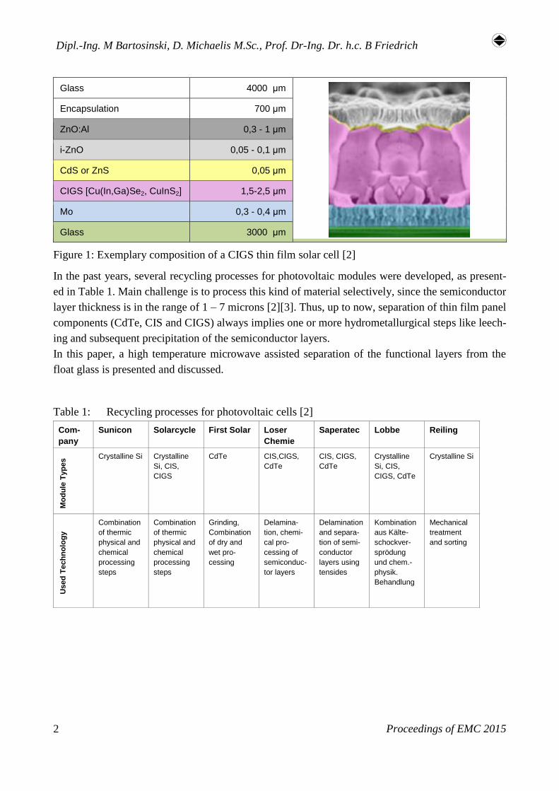
the last years. Beside silicon based photovoltaic modules (mono- and polycrystalline), Cadmium-
Telluride (CdTe) and Copper-Indium-(Gallium)-Diselenide (CIS or CIGS, see Figure 1) based pan-
els emerged as two popular technologies because of their relatively low manufacturing costs and
acceptable yields.
With continuously rising production rates, the demand for critical materials like Tellurium, Indium
and Gallium is growing. In addition to this, the life time cycle of a thin film solar panel does not
exceed 20-30 years, which will lead to a strong increase of scrap amounts in the next decades. As a
consequence, the European Union enhanced the WEEE directive committing the solar panel manu-
facturers to establish a Union wide recycling system. [1]
Dipl.-Ing. M Bartosinski, D. Michaelis M.Sc., Prof. Dr-Ing. Dr. h.c. B Friedrich
Proceedings of EMC 2015 2
Figure 1: Exemplary composition of a CIGS thin film solar cell [2]
In the past years, several recycling processes for photovoltaic modules were developed, as present-
ed in Table 1. Main challenge is to process this kind of material selectively, since the semiconductor
layer thickness is in the range of 1 – 7 microns [2][3]. Thus, up to now, separation of thin film panel
components (CdTe, CIS and CIGS) always implies one or more hydrometallurgical steps like leech-
ing and subsequent precipitation of the semiconductor layers.
In this paper, a high temperature microwave assisted separation of the functional layers from the
float glass is presented and discussed.
Table 1: Recycling processes for photovoltaic cells [2]
Com-
pany
Sunicon Solarcycle First Solar Loser
Chemie
Saperatec Lobbe Reiling
Mo
du
le T
yp
es Crystalline Si Crystalline
Si, CIS,
CIGS
CdTe CIS,CIGS,
CdTe
CIS, CIGS,
CdTe
Crystalline
Si, CIS,
CIGS, CdTe
Crystalline Si
Used
Te
ch
no
log
y
Combination
of thermic
physical and
chemical
processing
steps
Combination
of thermic
physical and
chemical
processing
steps
Grinding,
Combination
of dry and
wet pro-
cessing
Delamina-
tion, chemi-
cal pro-
cessing of
semiconduc-
tor layers
Delamination
and separa-
tion of semi-
conductor
layers using
tensides
Kombination
aus Kälte-
schockver-
sprödung
und chem.-
physik.
Behandlung
Mechanical
treatment
and sorting
Glass 4000 μm
Encapsulation 700 μm
ZnO:Al 0,3 - 1 μm
i-ZnO 0,05 - 0,1 μm
CdS or ZnS 0,05 μm
CIGS [Cu(In,Ga)Se2, CuInS2] 1,5-2,5 μm
Mo 0,3 - 0,4 μm
Glass 3000 μm
Seperation of semiconductor layers from thin film solar panels using microwave radiation
Proceedings of EMC 2015 3
Fundamentals
Microwaves (MW) are electromagnetic waves which cover frequencies from 300 MHz to 300 GHz
with corresponding wavelengths from λ =1 mm to 1 m. Since Microwaves follow the laws of op-
tics, they can be transmitted, absorbed or reflected by matter. [3] Although developed for military
use (radar, communication), MWs find a broad band of application as heating technology in differ-
ent industries.
In principle, the heating effect is based on the interaction of the electric and magnetic field with the
material to be heated. The electric field causes a polarization effect, i.e. an interfacial or dipolar
polarization. [4] These dipoles, however, are "unable" to meet the rapidly changing electric field
and generate heat. The magnetic field has been given no contribution to the warming in the past.
However, this is contradicted by recent studies. In fact, metals can be heated and even melted by
microwave radiation. Unlike in dielectrics, the penetration depth of the microwave in most metals is
only a few microns, which can be explained by the skin effect. The magnetic field causes eddy cur-
rents, which lead to a joule heating of the material. [4]. These interactions between microwaves and
metals were confirmed by several studies. [6][7][8][9]
Experimental
Goal of the presented work in this paper is to study the influence of MW radiation on the removal
of the semiconductor layers from CIGS solar panels. As stated before, thin film solar modules con-
sist of thin functional metal and semiconductor layers which are deposited on glass. Since glass is
transparent for microwaves, most of the absorbed energy will be dissipated as heat in the thin lay-
ers.
The experimental work took place in a controlled atmosphere microwave unit (constructed by
Fricke und Mallah Microwave Technology GmbH), which allows to run processes under high-
vacuum or inert gases. The test chamber of 650 mm diameter has the capability to handle batches in
kilogram-scale. The microwave unit is equipped with eight radial positioned magnetrons (micro-
wave generators) of 6 kW each to provide on-line adjustable power of max. 48 kW. The process is
observed by in situ video camera, temperature measures are monitored by an lR-camera placed on
the top of the furnace. This allows the study of heat distribution across the complete surface of the
charged material. The microwave unit is controlled by a custom designed LabVIEW Software. As
input material, CIGS panel fragments were used, which were detached from adhering organics (en-
capsulation material), since they would otherwise interfere with the process. Batches of approxi-
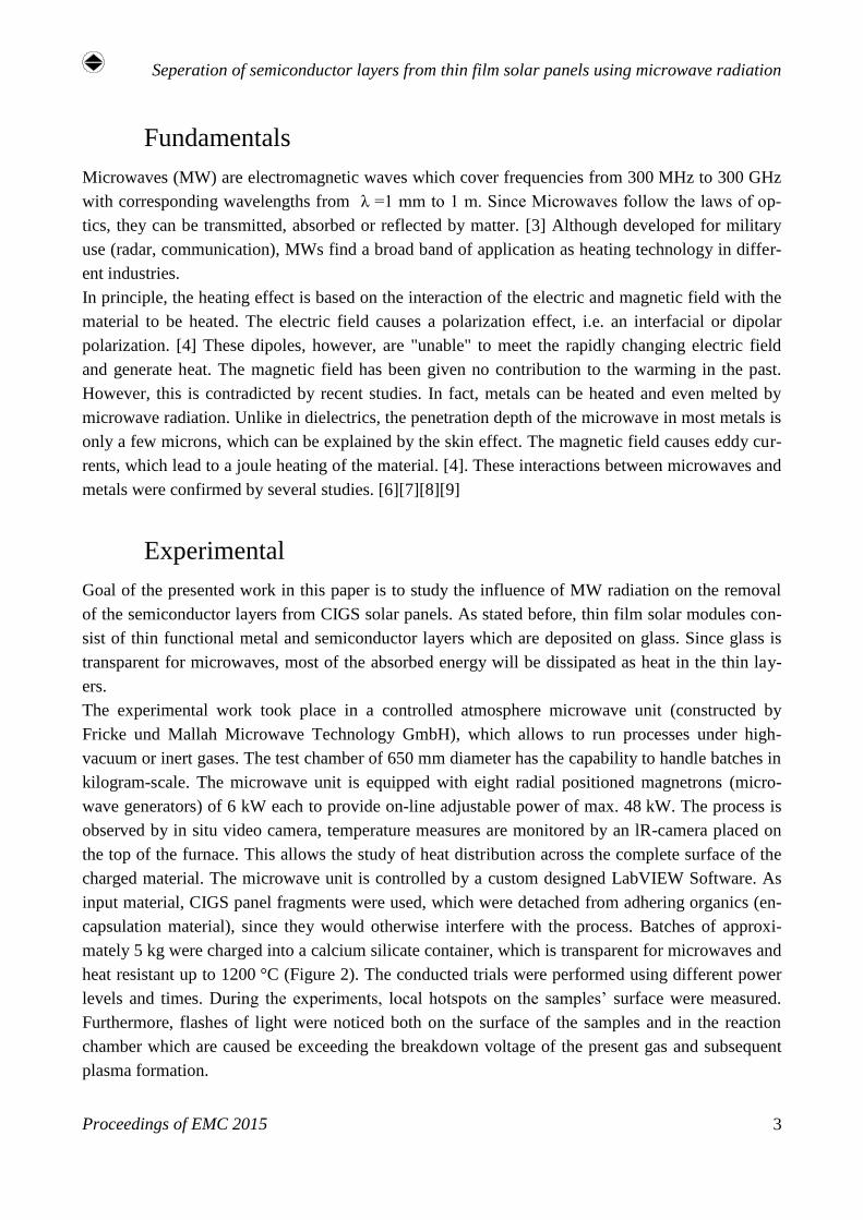
mately 5 kg were charged into a calcium silicate container, which is transparent for microwaves and
heat resistant up to 1200 °C (Figure 2). The conducted trials were performed using different power
levels and times. During the experiments, local hotspots on the samples’ surface were measured.
Furthermore, flashes of light were noticed both on the surface of the samples and in the reaction
chamber which are caused be exceeding the breakdown voltage of the present gas and subsequent
plasma formation.
Dipl.-Ing. M Bartosinski, D. Michaelis M.Sc., Prof. Dr-Ing. Dr. h.c. B Friedrich
Proceedings of EMC 2015 4
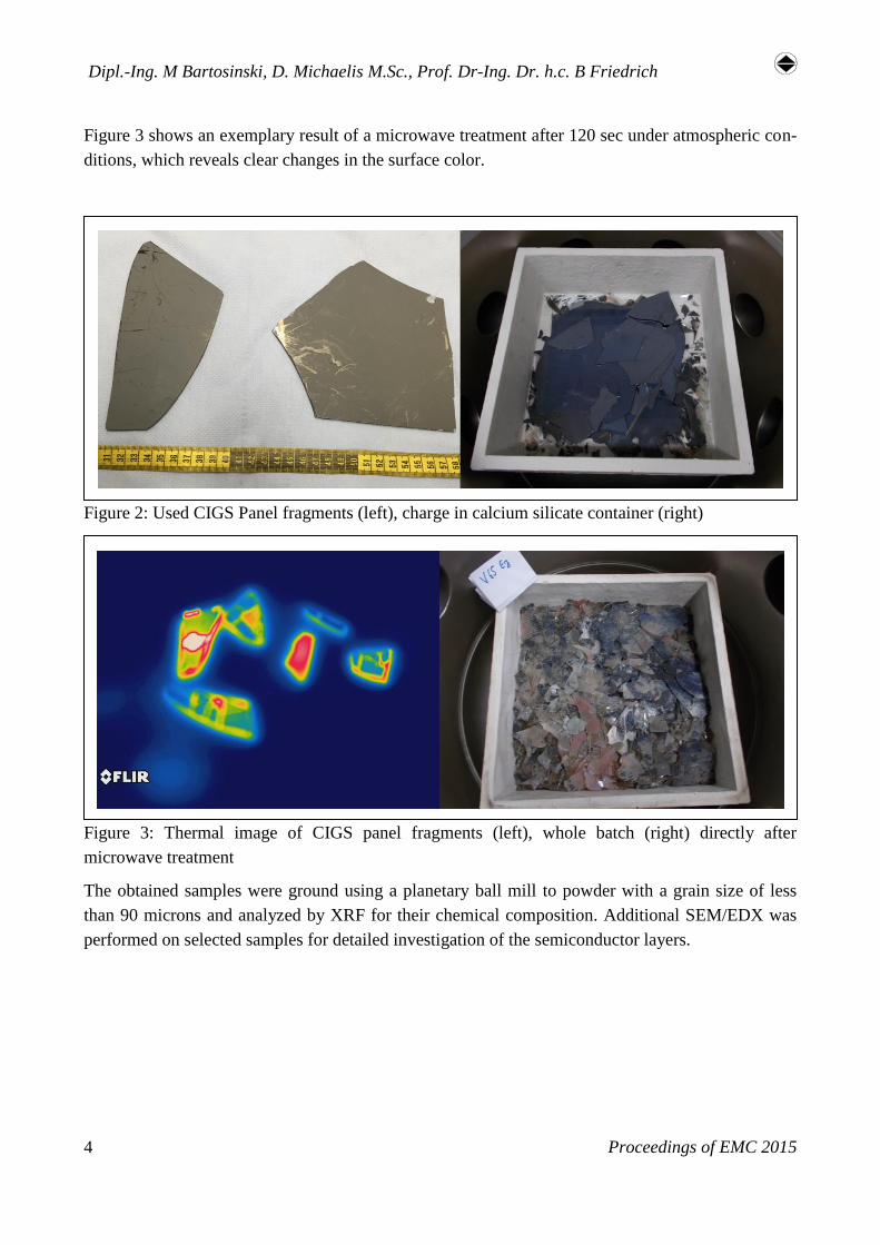
Figure 3 shows an exemplary result of a microwave treatment after 120 sec under atmospheric con-
ditions, which reveals clear changes in the surface color.
Figure 2: Used CIGS Panel fragments (left), charge in calcium silicate container (right)
Figure 3: Thermal image of CIGS panel fragments (left), whole batch (right) directly after
microwave treatment
The obtained samples were ground using a planetary ball mill to powder with a grain size of less
than 90 microns and analyzed by XRF for their chemical composition. Additional SEM/EDX was
performed on selected samples for detailed investigation of the semiconductor layers.
Seperation of semiconductor layers from thin film solar panels using microwave radiation
Proceedings of EMC 2015 5
Results and Discussion
The conducted experiments show a large scatter in terms of the removal of semiconductor layers,
which is mainly due to the inhomogeneous temperature distribution in the reactor. While maximum
surface temperatures of 350 °C depending on the power were measured in the center, panel frag-
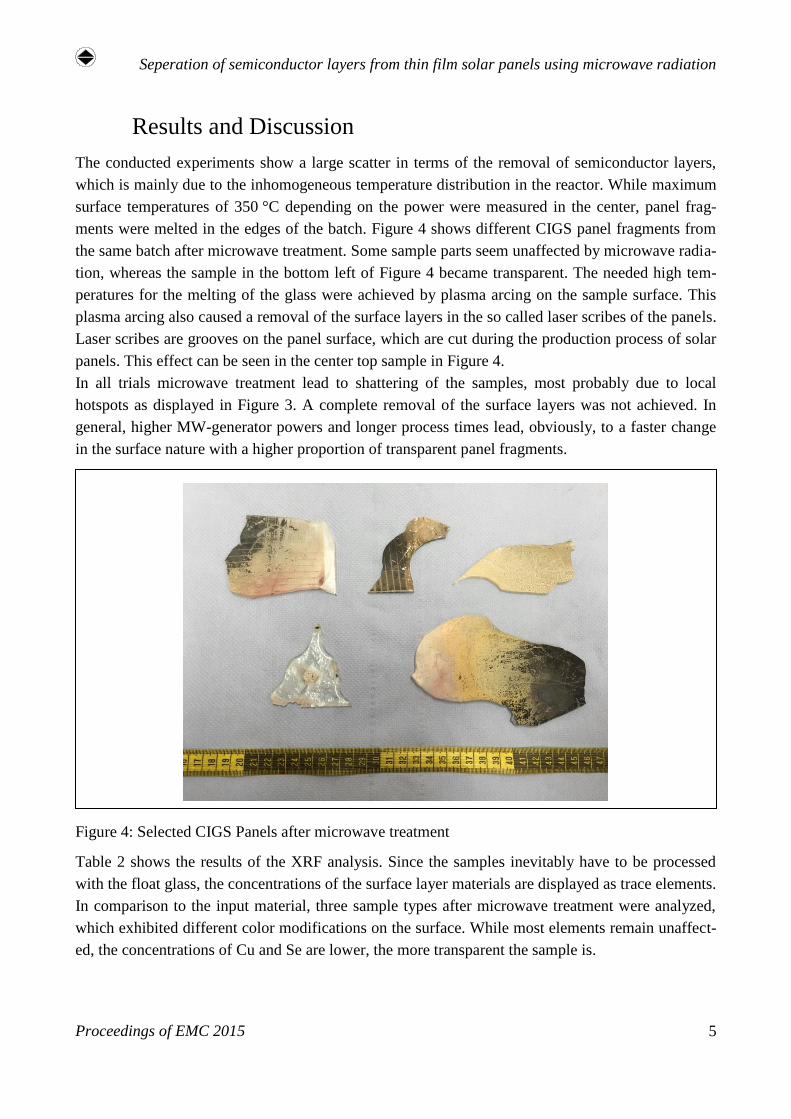
ments were melted in the edges of the batch. Figure 4 shows different CIGS panel fragments from
the same batch after microwave treatment. Some sample parts seem unaffected by microwave radia-
tion, whereas the sample in the bottom left of Figure 4 became transparent. The needed high tem-
peratures for the melting of the glass were achieved by plasma arcing on the sample surface. This
plasma arcing also caused a removal of the surface layers in the so called laser scribes of the panels.
Laser scribes are grooves on the panel surface, which are cut during the production process of solar
panels. This effect can be seen in the center top sample in Figure 4.
In all trials microwave treatment lead to shattering of the samples, most probably due to local
hotspots as displayed in Figure 3. A complete removal of the surface layers was not achieved. In
general, higher MW-generator powers and longer process times lead, obviously, to a faster change
in the surface nature with a higher proportion of transparent panel fragments.
Figure 4: Selected CIGS Panels after microwave treatment
Table 2 shows the results of the XRF analysis. Since the samples inevitably have to be processed
with the float glass, the concentrations of the surface layer materials are displayed as trace elements.
In comparison to the input material, three sample types after microwave treatment were analyzed,
which exhibited different color modifications on the surface. While most elements remain unaffect-
ed, the concentrations of Cu and Se are lower, the more transparent the sample is.
Dipl.-Ing. M Bartosinski, D. Michaelis M.Sc., Prof. Dr-Ing. Dr. h.c. B Friedrich
Proceedings of EMC 2015 6
Table 2: Trace elements concentration of CIGS material before and after microwave treatment
Cu
ppm
Ga
ppm
In
ppm
Se
ppm
Mo
ppm
Sn
ppm
Zn
ppm
CIGS (input) 311 62 250 364 288 36 10
CIGS (brown) 320 46 190 144 282 39 12
CIGS (red) 218 68 240 8 269 39 10
CIGS (transparent) 152 49 160 8 285 37 10
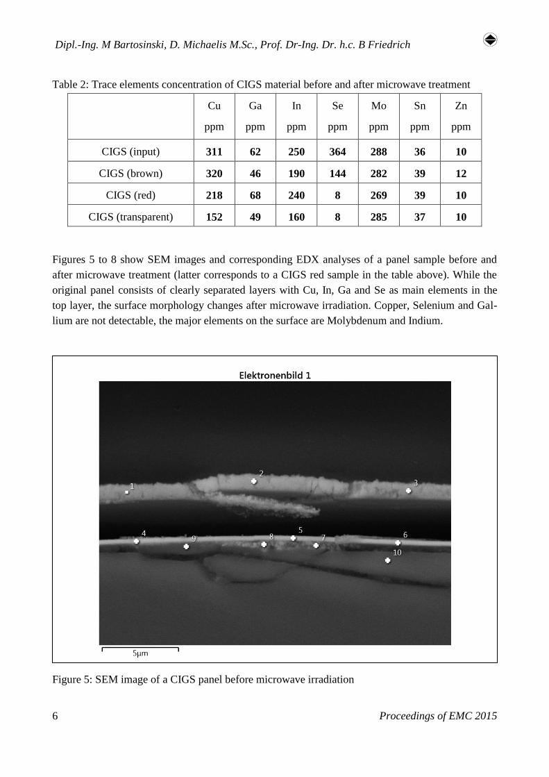
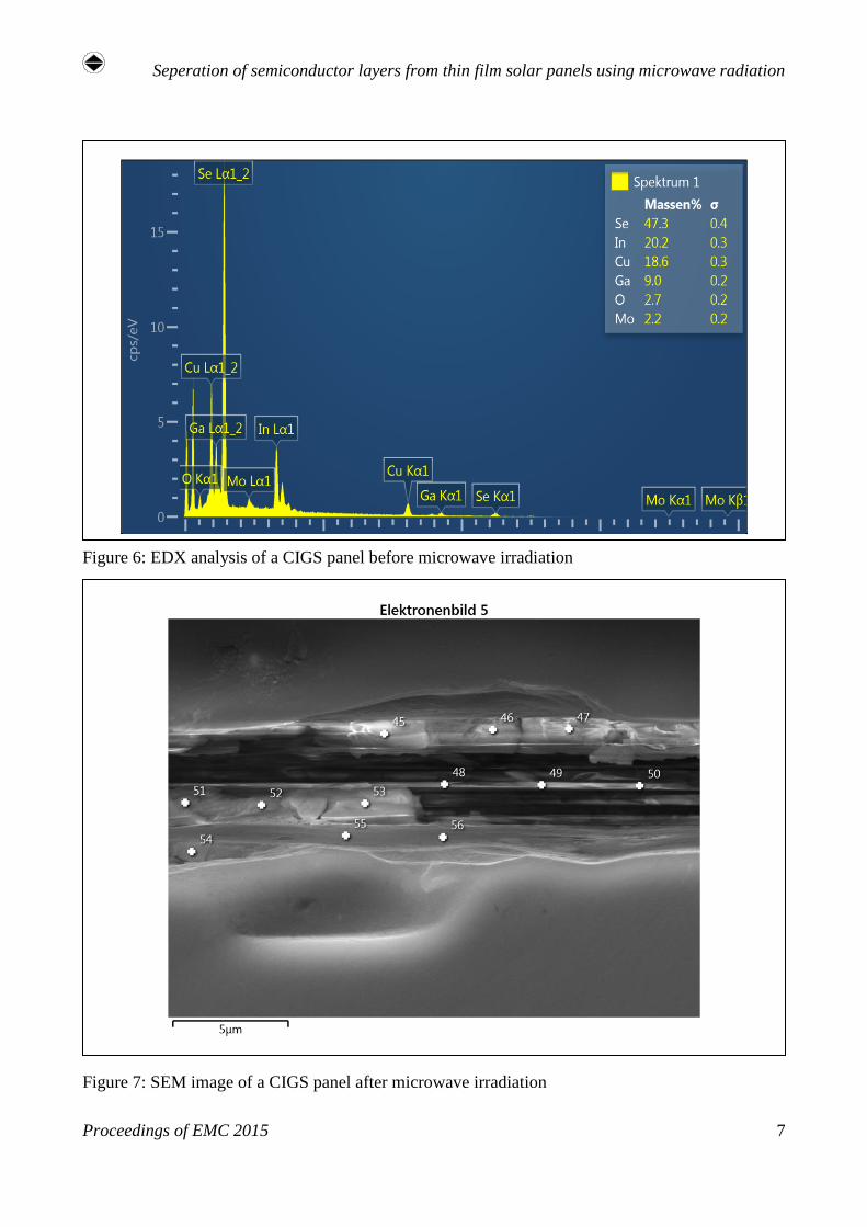
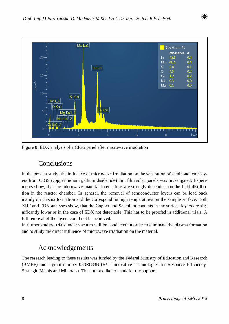
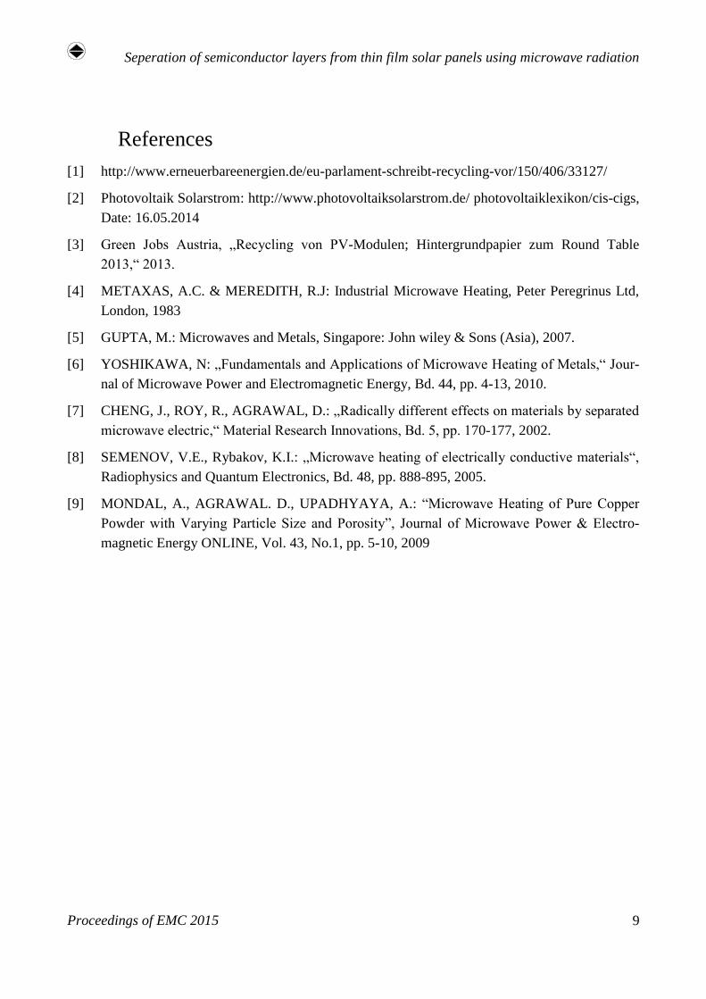
Figures 5 to 8 show SEM images and corresponding EDX analyses of a panel sample before and
after microwave treatment (latter corresponds to a CIGS red sample in the table above). While the
original panel consists of clearly separated layers with Cu, In, Ga and Se as main elements in the
top layer, the surface morphology changes after microwave irradiation. Copper, Selenium and Gal-
lium are not detectable, the major elements on the surface are Molybdenum and Indium.
Figure 5: SEM image of a CIGS panel before microwave irradiation
Seperation of semiconductor layers from thin film solar panels using microwave radiation
Proceedings of EMC 2015 7
Figure 6: EDX analysis of a CIGS panel before microwave irradiation
Figure 7: SEM image of a CIGS panel after microwave irradiation
Dipl.-Ing. M Bartosinski, D. Michaelis M.Sc., Prof. Dr-Ing. Dr. h.c. B Friedrich
Proceedings of EMC 2015 8
Figure 8: EDX analysis of a CIGS panel after microwave irradiation
Conclusions
In the present study, the influence of microwave irradiation on the separation of semiconductor lay-
ers from CIGS (copper indium gallium diselenide) thin film solar panels was investigated. Experi-
ments show, that the microwave-material interactions are strongly dependent on the field distribu-
tion in the reactor chamber. In general, the removal of semiconductor layers can be lead back
mainly on plasma formation and the corresponding high temperatures on the sample surface. Both
XRF and EDX analyses show, that the Copper and Selenium contents in the surface layers are sig-
nificantly lower or in the case of EDX not detectable. This has to be proofed in additional trials. A
full removal of the layers could not be achieved.
In further studies, trials under vacuum will be conducted in order to eliminate the plasma formation
and to study the direct influence of microwave irradiation on the material.
Acknowledgements
The research leading to these results was funded by the Federal Ministry of Education and Research
(BMBF) under grant number 033R083B (R³ - Innovative Technologies for Resource Efficiency-
Strategic Metals and Minerals). The authors like to thank for the support.
Seperation of semiconductor layers from thin film solar panels using microwave radiation
Proceedings of EMC 2015 9
References
[1] http://www.erneuerbareenergien.de/eu-parlament-schreibt-recycling-vor/150/406/33127/
[2] Photovoltaik Solarstrom: http://www.photovoltaiksolarstrom.de/ photovoltaiklexikon/cis-cigs,
Date: 16.05.2014
[3] Green Jobs Austria, „Recycling von PV-Modulen; Hintergrundpapier zum Round Table
2013,“ 2013.
[4] METAXAS, A.C. & MEREDITH, R.J: Industrial Microwave Heating, Peter Peregrinus Ltd,
London, 1983
[5] GUPTA, M.: Microwaves and Metals, Singapore: John wiley & Sons (Asia), 2007.
[6] YOSHIKAWA, N: „Fundamentals and Applications of Microwave Heating of Metals,“ Jour-
nal of Microwave Power and Electromagnetic Energy, Bd. 44, pp. 4-13, 2010.
[7] CHENG, J., ROY, R., AGRAWAL, D.: „Radically different effects on materials by separated
microwave electric,“ Material Research Innovations, Bd. 5, pp. 170-177, 2002.
[8] SEMENOV, V.E., Rybakov, K.I.: „Microwave heating of electrically conductive materials“,
Radiophysics and Quantum Electronics, Bd. 48, pp. 888-895, 2005.
[9] MONDAL, A., AGRAWAL. D., UPADHYAYA, A.: “Microwave Heating of Pure Copper
Powder with Varying Particle Size and Porosity”, Journal of Microwave Power & Electro-
magnetic Energy ONLINE, Vol. 43, No.1, pp. 5-10, 2009