Embed Size (px)
Citation preview

Visit www.gansystems.com for the latest version of this user’s guide.
This evaluation kit is designed for engineering evaluation in a controlled
lab environment and should be handled by qualified personnel ONLY.
High voltage will be exposed on the board during the test and even brief
contact during operation may result in severe injury or death.
Never leave the board operating unattended. After it is de-energized,
always wait until all capacitors are discharged before touching the board.
This product contains parts that are susceptible to damage by electrostatic
discharge (ESD). Always follow ESD prevention procedures when
handling the product.

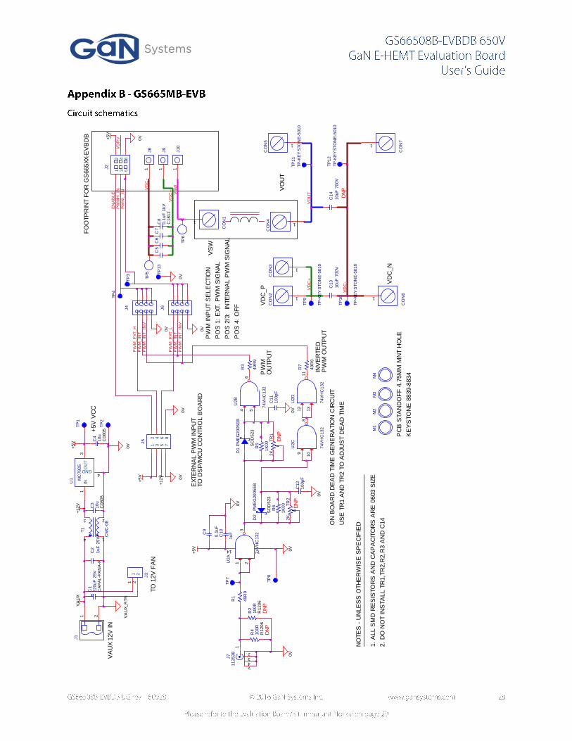
The GS665XXX-EVBDB daughter board style evaluation kit consists of two GaN Systems 650V GaN
Enhancement-mode HEMTs (E-HEMTs) and all necessary circuits including half bridge gate drivers,
isolated power supplies and optional heatsink to form a functional half bridge power stage. It allows
users to easily evaluate the GaN E-HEMT performance in any half bridge-based topology, either with the
universal mother board (P/N: GS665MB-EVB) or users’ own system design.
Serves as a reference design and evaluation tool as well as deployment-ready solution for easy in-
system evaluation.
Vertical mount style with height of 35mm, which fits in majority of 1U design and allows
evaluation of GaN E-HEMT in traditional through-hole type power supply board.
Current shunt position for switching characterization testing
Universal form factor and footprint for all products
The daughter board and universal mother board ordering part numbers are below:
Part Number GaN E-HEMT P/N: Description
GS66502B-EVBDB GS66502B GaN E-HEMT 650V/7.5A, 200mΩ
GS66504B-EVBDB GS66504B GaN E-HEMT 650V/15A, 100mΩ
GS66508B-EVBDB GS66508B GaN E-HEMT 650V/30A, 50mΩ
GS66508T-EVBDB GS66508T GaN E-HEMT top side cooled 650V/30A, 50mΩ
GS66516T-EVBDB GS66516T GaN E-HEMT top side cooled 650V/60A, 25mΩ
GS665MB-EVB Universal 650V Mother Board
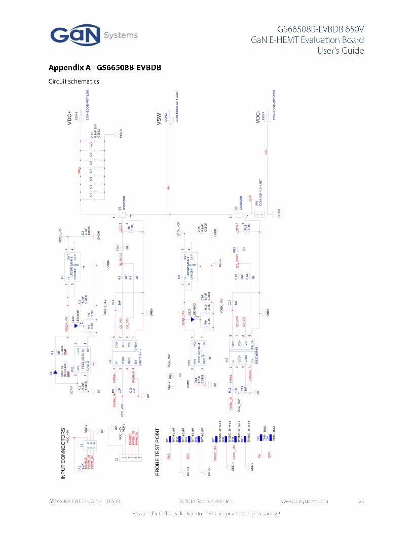
The daughter board GS665XXX-EVBDB circuit diagram is shown in Figure 1. The control logic inputs on
2x3 pin header J1 are listed below:
Pin Descriptipon
ENA Enable input. It is internally pulled up to VCC, a low logic disables all the PWM gate
drive outputs.
VCC +5V auxillary power supply input for logic circuit and gate driver. On the daughter
board there are 2 isolated 5V to 9V DC/DC power supplies for top and bottom switches.
VDRV Optional 9V gate drive power input. This pin allows users to supply separate gate drive
power supply. By default VDRV is connected to VCC on the daughter board via a 0 ohm
jumper FB1. If bootstrap mode is used for high side gate drive, connect VDRV to 9V
PWMH High side PWM logic input for top switch Q1. It is compatible wth 3.3V and 5V
PWML Low side PWM logic input for bottom switch Q2. It is compatible wth 3.3V and 5V
0V Logic inputs and gate drive power supply ground return.
The 3 power pins are:
VDC+: Input DC Bus voltage
VSW: Switching node output
VDC-: Input DC bus voltage ground return. Note that control ground 0V is isolated from VDC-.
Si8271 Iso.
Gate DriverQ1
Q2Si8271 Iso.
Gate Driver
Iso. DC/DC
or Bootstrap
Iso. DC/DC
VDC+
VSW
VDC-
VCC
ENABLE
JP1
C4-10
PWMH
PWML

A. 2x GaN Systems 650V E-HEMT GS66508B, 30A/50mΩ
B. Decoupling capacitors C4-C11
C. Isolated gate driver Silab Si8271GB-IS
D. Optional current shunt position JP1.
E. Test points for bottom Q2 VGS.
F. Recommended probing positions for Q2 VDS.
G. Optional bootstrap circuit D1/R1 (unpopulated).
H. 5V-9V isolated DC/DC gate drive power supply
This daughter board includes two GaN Systems E-HEMT GS66508B (650V/30A, 50mΩ) in a
GaNPx™ B type package. The large S pad serves as source connection and thermal pad. The pin
4 is the kelvin source connection for gate drive return.

Silab Si8271GB-IS isolated gate driver is chosen for this design. This driver is compatible with 6V
gate drive with 4V UVLO and has CMTI dv/dt rating up to 200V/ns. It has separated source and
sink drive outputs which eliminates the need for additional diode.
GaN E-HEMT switching speed and slew rate can be directly controlled by the gate resistor. By
default the turn-on Rgate (R6/R12) is 10Ω and Rg_off (R7/R14) is 1Ω. User can adjust the values
of gate resistors to fine tune the turn-on and off speed.
FB1/FB2 are footprints for optional ferrite bead. By default they are populated with 0Ω jumpers.
If gate oscillation is observed, it is recommended to replace them with ferrite bead with Z=10-
20Ω@100MHz.
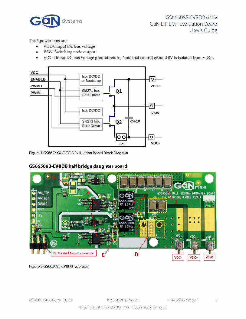
5V-9V isolated DC/DC converters are used for gate drive. 9V output is then regulated down to
6V for gate driver.
By default gate drive supply input VDRV is tied to VCC +5V via 0Ω jumper (FB1). Remove FB1 if
separate gate drive input voltage is to be used.
The board has option for users to experiment with non-isolated bootstrap circuit with following
circuit changes:
o Remove PS2 and short circuit pin 2 to 5 and pin 1 to 4.
o Populate D1/ R1 (not supplied): D1 is the high voltage bootstrap diode (for example ES1J)
and use 1-2Ω 0805 SMD resistor on R1. Depopulate PS1, LED1 and replace C2 with 1uF
capacitor.
o Remove 0Ω jumper at FB1 and supply +9V at VDRV.
U2
SI8271GB-IS
VI1
VDDI2
GNDI3
EN4
GNDA5
VO-6
VO+7
VDD8PWMH
R83.3K
Q1G
ENABLE
FB2
0R
Q1
GS66508B
1
2
4
3
R6
10R
R7
1R
Q1_GOUT
PWMH_INR5
10R Q1_VO+
Q1_VO-
GNDH
C12
1uF
VDDH_+6V
C131uF
VCC_+5V
0V
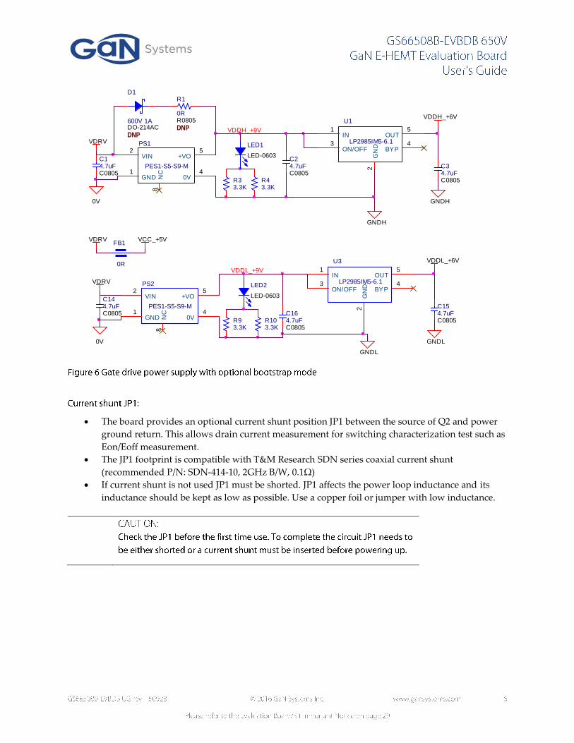
The board provides an optional current shunt position JP1 between the source of Q2 and power
ground return. This allows drain current measurement for switching characterization test such as
Eon/Eoff measurement.
The JP1 footprint is compatible with T&M Research SDN series coaxial current shunt
(recommended P/N: SDN-414-10, 2GHz B/W, 0.1Ω)
If current shunt is not used JP1 must be shorted. JP1 affects the power loop inductance and its
inductance should be kept as low as possible. Use a copper foil or jumper with low inductance.
D1
600V 1ADO-214AC
R1
0RR0805
DNPDNP
PS1
PES1-S5-S9-M
GND1
VIN2
+VO5
0V4
NC
8
U1
LP2985IM5-6.1IN
1
GN
D2
ON/OFF3
BYP4
OUT5
GNDH
0V
VDRV
C14.7uFC0805
VDDH_+6V
C34.7uFC0805
GNDH
R43.3K
C24.7uFC0805
R33.3K
LED1
LED-0603
VDDH_+9V
PS2
PES1-S5-S9-M
GND1
VIN2
+VO5
0V4
NC
8
GNDL
U3
LP2985IM5-6.1IN
1
GN
D2
ON/OFF3
BYP4
OUT5
0V
VDRV
C144.7uFC0805
VDDL_+6V
C154.7uFC0805
GNDL
C164.7uFC0805
R93.3K
LED2
LED-0603
VDDL_+9V
FB1
0R
VDRV VCC_+5V
R103.3K
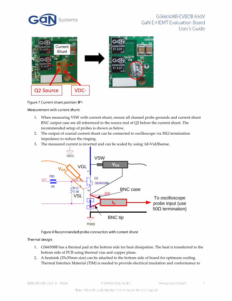
1. When measuring VSW with current shunt, ensure all channel probe grounds and current shunt
BNC output case are all referenced to the source end of Q2 before the current shunt. The
recommended setup of probes is shown as below.
2. The output of coaxial current shunt can be connected to oscilloscope via 50Ω termination
impedance to reduce the ringing.
3. The measured current is inverted and can be scaled by using: Id=Vid/Rsense.
1. GS66508B has a thermal pad at the bottom side for heat dissipation. The heat is transferred to the
bottom side of PCB using thermal vias and copper plane.
2. A heatsink (35x35mm size) can be attached to the bottom side of board for optimum cooling.
Thermal Interface Material (TIM) is needed to provide electrical insulation and conformance to
VGL
VSL
VSW
BNC case
To oscilloscope
probe input (use
50Ω termination)
BNC tip
VDS
VGS
ID

the PCB surface. The daughter board evaluation kit supplies with a sample 35x35mm fin heatsink
(not installed), although other heatsinks can also be used to fit users’ system design.
3. A thermal tape type TIM (Berguist® Bond-Ply 100) is chosen for its easy assembly. The supplied
heatsink has the thermal tape pre-applied so simply peel off the protective film and attach the
heatsink to the back of board as marked in Figure 3.
4. Two optional mounting holes as shown in Figure 9 are provided for mounting customized
heatsink using screws.
5. Using the supplied heatsink and TIM, the overall junction to ambient thermal resistance RthJ-A is
~9°C/W with 500LFM airflow.
6. Forced air cooling is recommended for power testing.
°

GaN Systems provides a universal 650V mother board (ordering part number: GS665MB-EVB, sold
separately) that can be used as the basic evaluation platform for all the daughter boards.
The universal 650V mother board evaluation kit includes following items:
1. Mother board GS665MB-EVB
2. 12VDC Fan
The board can be powered by 9-12V on J1. On-board voltage regulator creates to 5V for daughter board
and control logic circuits. J3 is used for external 12VDC fan.
12V INPUT
(+)5V Power Supply
CIN
VSW
PWM control & dead
time circuit
Daughter Board
Probing point for VSW
For Ext.
12VDC Fan
Airflow direction
Optional CoutVDC- VOUT
VDC-
VDC+
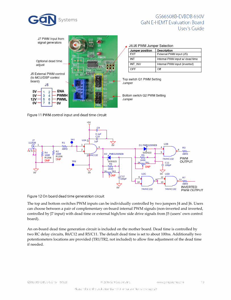
The top and bottom switches PWM inputs can be individually controlled by two jumpers J4 and J6. Users
can choose between a pair of complementary on-board internal PWM signals (non-inverted and inverted,
controlled by J7 input) with dead time or external high/low side drive signals from J5 (users’ own control
board).
An on-board dead time generation circuit is included on the mother board. Dead time is controlled by
two RC delay circuits, R6/C12 and R5/C11. The default dead time is set to about 100ns. Additionally two
potentiometers locations are provided (TR1/TR2, not included) to allow fine adjustment of the dead time
if needed.
0V
D1 PMEG2005EB
SOD523
R6
1K00
TR12K C11100pF
0V
R5
1K00
C10
1uF
C9
0.1uF
+5V
J7112538
1
2345
R4100RR1206
R2100RR1206
U2A
74VHC132
31
2
14
7
0V
R1
49R9
0V
D2 PMEG2005EB
SOD523
TR22K
C12100pF
0V
U2B
74VHC132
4
56
U2C
74VHC132
9
108
U2D
74VHC132
12
1311
TP7
TP8
DNP
DNP
PWM OUTPUT
INVERTED PWM OUTPUT
R3
49R9
DNPDNP
R7
49R9

Test points are designed in groups/pairs to facilitate probing:
Test points Name Description
TP1/TP2 +5V/0V 5V bias power
TP7/TP8 PWMIN/0V PWM input signal from J7
TP4/TP3/TP13 PWMH/PWML/0V High/low side gate signals to daughter board
TP9/TP10 VDC+/VDC- DC bus voltage
TP11/TP12 VOUT/VDC- Output voltage
TP6/TP5 VSW/VDC- Switching node output voltage (for HV oscilloscope
probe)
CON1-CON7 mounting pads are designed to be compatible with following mounting terminals:
#10-32 Screw mount,
Banana Jack PCB mount (Keystone P/N: 575-4), or
PC Mount Screw Terminal (Keystone P/N: 8191)
An external power inductor (not included) can be connected between VSW (CON1) and VOUT (CON4/5)
or VDC+ (CON2/3) for double pulse test. Users can choose their inductor size to meet the test
requirement. Generally it is recommended to use power inductor with low inter-winding capacitance to
obtain best switching performance. For the double pulse testing we use 2x 60uH/40Amp inductor (CWS,
P/N: HF467-600M-40AV) in series. C14 is designed to accommodate a film capacitor as output filter.
CON1
Q1
CON2
Q2
VDC-
CON4
CON3
LOUT
400V DC
+
VDC+
CON7CON6
VSW
CON5
+5V
0V
PWM
INPUT
(J7)
VDS
IL
ISW
VGL
+6V
0VVDS
VGL
IL
t0 t1 t2 t3TON1
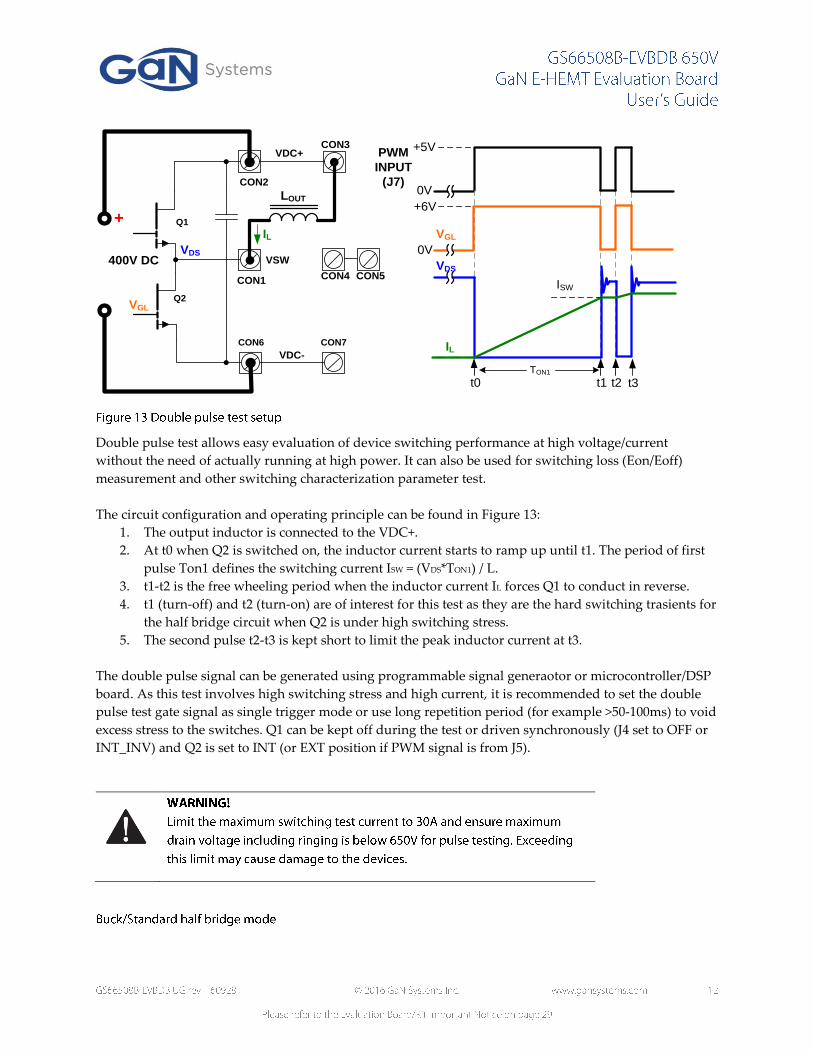
Double pulse test allows easy evaluation of device switching performance at high voltage/current
without the need of actually running at high power. It can also be used for switching loss (Eon/Eoff)
measurement and other switching characterization parameter test.
The circuit configuration and operating principle can be found in Figure 13:
1. The output inductor is connected to the VDC+.
2. At t0 when Q2 is switched on, the inductor current starts to ramp up until t1. The period of first
pulse Ton1 defines the switching current ISW = (VDS*TON1) / L.
3. t1-t2 is the free wheeling period when the inductor current IL forces Q1 to conduct in reverse.
4. t1 (turn-off) and t2 (turn-on) are of interest for this test as they are the hard switching trasients for
the half bridge circuit when Q2 is under high switching stress.
5. The second pulse t2-t3 is kept short to limit the peak inductor current at t3.
The double pulse signal can be generated using programmable signal generaotor or microcontroller/DSP
board. As this test involves high switching stress and high current, it is recommended to set the double
pulse test gate signal as single trigger mode or use long repetition period (for example >50-100ms) to void
excess stress to the switches. Q1 can be kept off during the test or driven synchronously (J4 set to OFF or
INT_INV) and Q2 is set to INT (or EXT position if PWM signal is from J5).
CON1
Q1
CON2
Q2
VDC-
CON4
CON3
LOUT
400V DC
+
VDC+
CON7
CON6
VSW
CON5
COUT RLoad
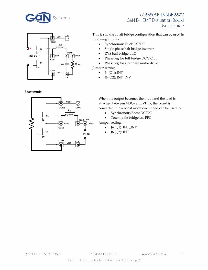
This is standard half bridge configuration that can be used in
following circuits :
Synchronous Buck DC/DC
Single phase half bridge inverter
ZVS half bridge LLC
Phase leg for full bridge DC/DC or
Phase leg for a 3-phase motor drive
Jumper setting:
J4 (Q1): INT
J6 (Q2): INT_INV
CON1
Q1
CON2
Q2
VDC-
CON4
CON3
LIN
VDC+
CON7CON6
VSW
CON5
INPUT
VIN
When the output becomes the input and the load is
attached between VDC+ and VDC-, the board is
converted into a boost mode circuit and can be used for:
Synchronous Boost DC/DC
Totem pole bridgeless PFC
Jumper setting:
J4 (Q1): INT_INV
J6 (Q2): INT
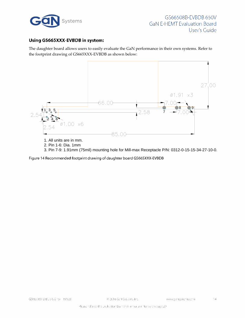
The daughter board allows users to easily evaluate the GaN performance in their own systems. Refer to
the footprint drawing of GS665XXX-EVBDB as shown below:
1 3 5
2 4 6
78 9
1. All units are in mm.
2. Pin 1-6: Dia. 1mm
3. Pin 7-9: 1.91mm (75mil) mounting hole for Mill-max Receptacle P/N: 0312-0-15-15-34-27-10-0.

Follow the instructions below to quickly get started with your evaluation of GaN E-HEMT. Equipment
and components you will need:
Four-channel oscilloscope with 500MHz bandwidth or higher
high bandwidth (500MHz or higher) passive probe
high bandwidth (500MHz) high voltage probe (>600V)
AC/DC current probe for inductor current measurement
12V DC power supply
Signal generator capable of creating testing pulses
High voltage power supply (0-400VDC) with current limit.
External power inductor (recommend toroid inductor 50-200uH)
1. Check the JP1 on daughter board GS665XXX-EVBDB. Use a copper foil and solder to short JP1.
2. Install GS665XXX-EVBDB on the mother board. Press all the way down until you feel a click. Connect
probe between VGL and VSL for gate voltage measurement.
3. Set up the mother board:
a. Connect 12VDC bias supply to J1.
b. Connect PWM input gate signal (0-5V) to J7. If it is generated from a signal generator ensure
the output mode is high-Z mode.
c. Set J4 to OFF position and J7 to INT.
d. Set High voltage (HV) DC supply voltage to 0V and ensure the output is OFF. Connect HV
supply to CON2 and CON6.
e. Use HV probe between TP6 and TP5 for Vds measurement.
f. Connect external inductor between CON1 and CON3. Use current probe to measure inductor
current IL.
4. Set up and check PWM gate signal:
a. Turn-on 12VDC power.
b. Check the 2 LEDs on the daughter board. They should be turned on indicating the isolated
9V is present.
c. Set up signal generator to create the waveforms as shown in Figure 13. Use equation ISW =
(VDS*TON1) / L to calculate the pulse width of the first pulse and ensure the Isw_max is ≤30A at
400VDC.
d. Set the operation mode to either single trigger or Burst mode with repetition period of 100ms.
e. Turn on the PWM output and check on the oscilloscope to make sure the VGL waveform is
present and matches the PWM input.
5. Power-on:
a. Turn on the output of the HV supply. Start with low voltage and slowly ramp the voltage up
until it reaches 400VDC. During the ramping period closely observe the the voltage and
current waveforms on the oscilloscope.
6. Power-off:
a. After the test is complete, slowly ramp down the HV supply voltage to 0V and turn off the
output. Then turn off the 12V bias supply and signal generator output.
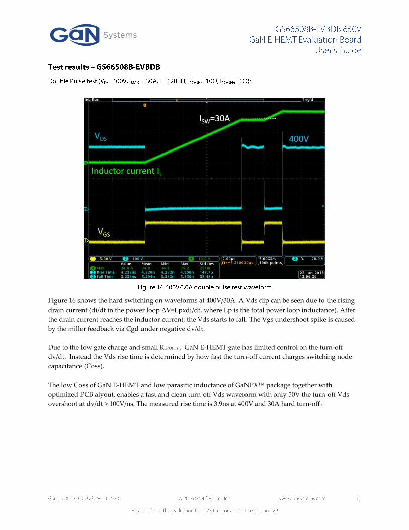
Figure 16 shows the hard switching on waveforms at 400V/30A. A Vds dip can be seen due to the rising
drain current (di/dt in the power loop ΔV=Lpxdi/dt, where Lp is the total power loop inductance). After
the drain current reaches the inductor current, the Vds starts to fall. The Vgs undershoot spike is caused
by the miller feedback via Cgd under negative dv/dt.
Due to the low gate charge and small RG(OFF) , GaN E-HEMT gate has limited control on the turn-off
dv/dt. Instead the Vds rise time is determined by how fast the turn-off current charges switching node
capacitance (Coss).
The low Coss of GaN E-HEMT and low parasitic inductance of GaNPX™ package together with
optimized PCB alyout, enables a fast and clean turn-off Vds waveform with only 50V the turn-off Vds
overshoot at dv/dt > 100V/ns. The measured rise time is 3.9ns at 400V and 30A hard turn-off。
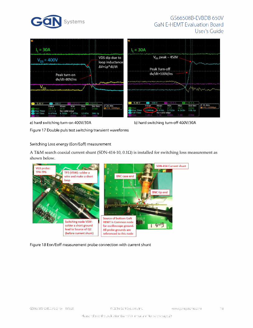
A T&M search coaxial current shunt (SDN-414-10, 0.1Ω) is installed for switching loss measurement as
shown below.
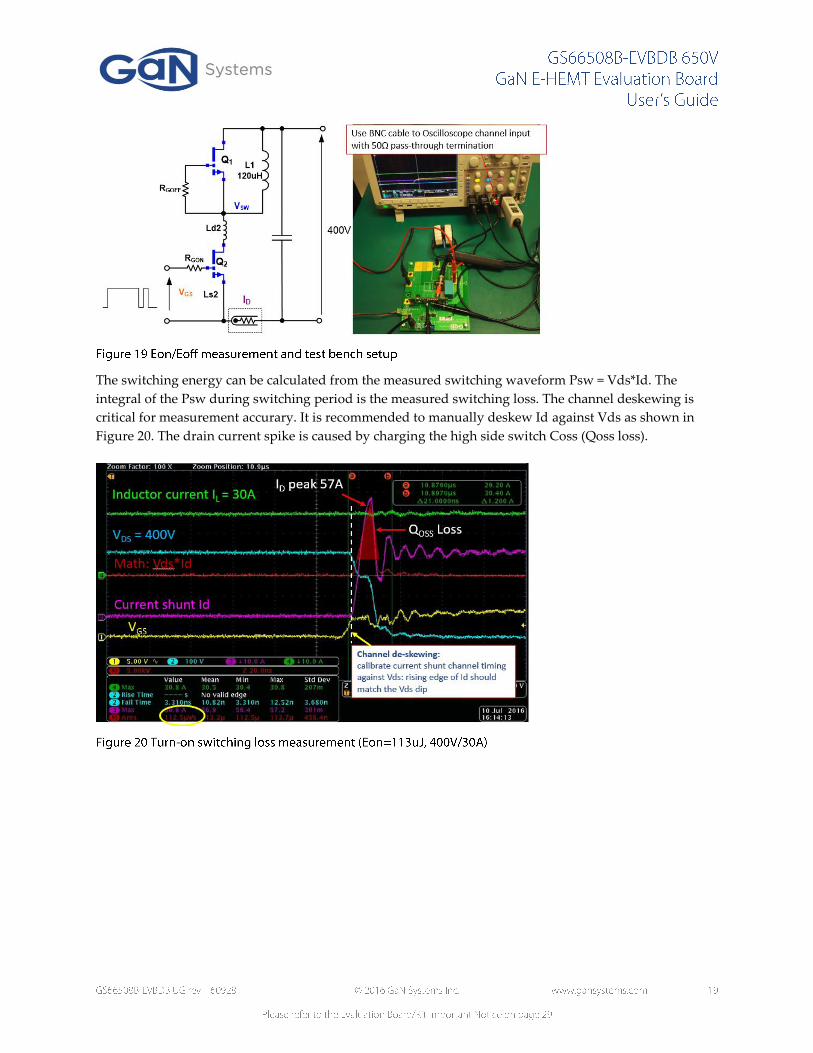
The switching energy can be calculated from the measured switching waveform Psw = Vds*Id. The
integral of the Psw during switching period is the measured switching loss. The channel deskewing is
critical for measurement accurary. It is recommended to manually deskew Id against Vds as shown in
Figure 20. The drain current spike is caused by charging the high side switch Coss (Qoss loss).

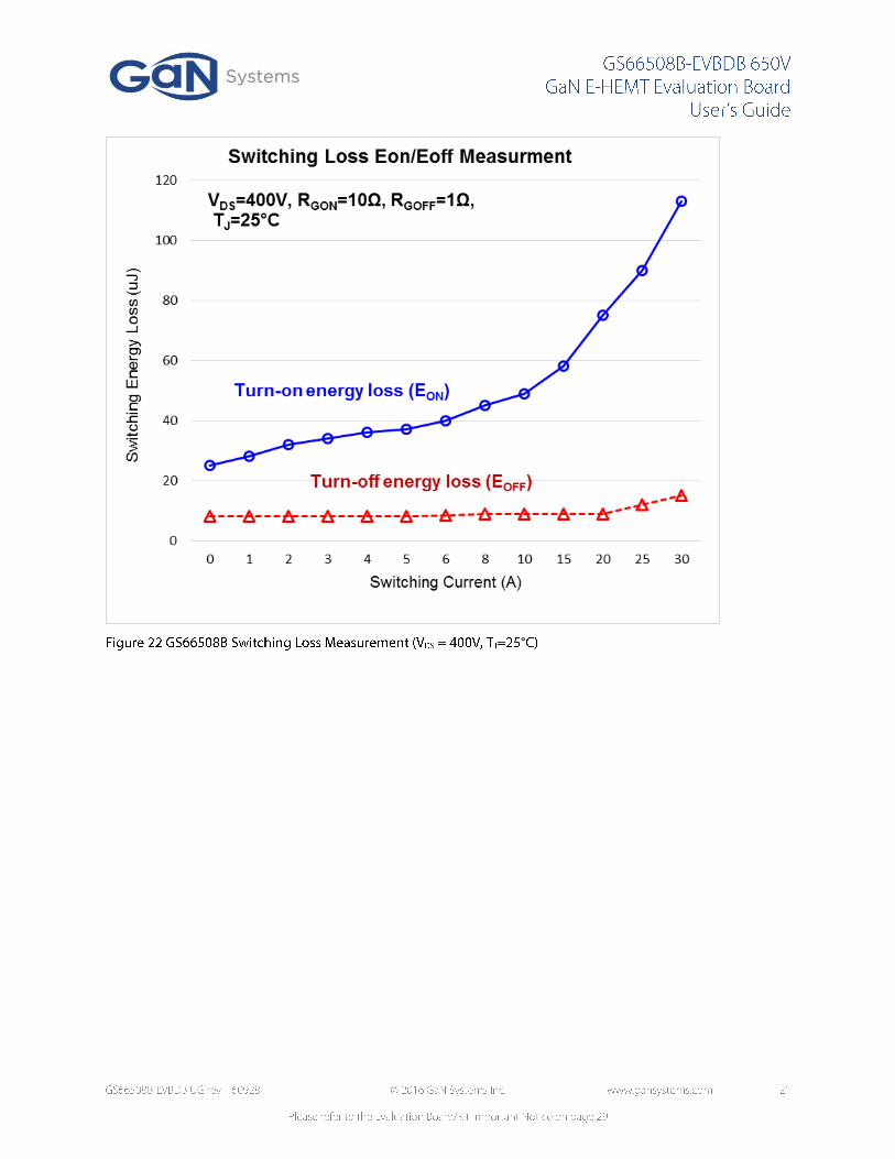
The switching loss measurements with drain current from 0 to 30A can be found in Figure 22. The turn-
on loss dominates the overall hard switching loss. Eon at 0A is the Qoss loss caused by the Coss at high
side switch.
The turn-off loss remain almost constant from 0A up to 20A about 8uJ. the measured Eoff matches well
with the Eoss @400V, which indicates that turn-off energy is dominated by Eoss, the energy required to
charge Coss from 0V to bus voltage. This energy is not part of loss at turn-off, but actually part of turn-on
loss at next hard switching turn-on period. This means that with the fast turn-off speed the GaN E-HEMT
can achieve near zero turn-off switching loss.
°
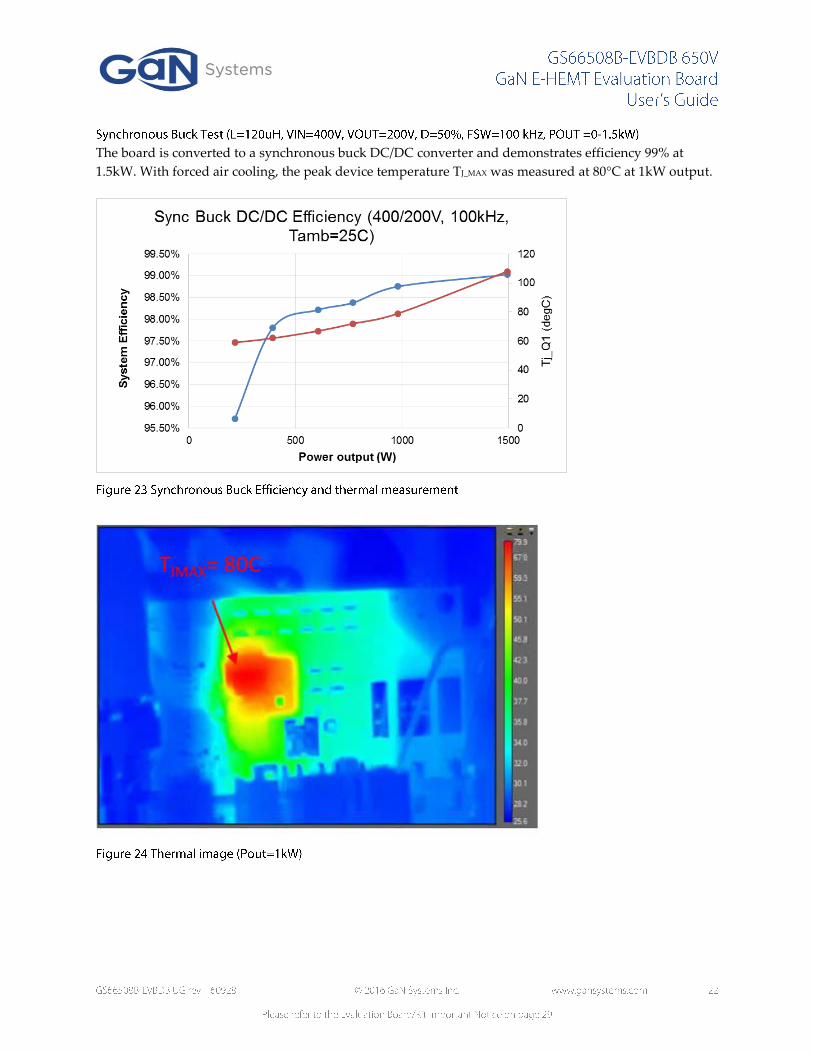
The board is converted to a synchronous buck DC/DC converter and demonstrates efficiency 99% at
1.5kW. With forced air cooling, the peak device temperature TJ_MAX was measured at 80°C at 1kW output.
TP
1
TP
TH
-1M
M
PS
2 PE
S1-S
5-S
9-M
GN
D1
VIN
2+V
O5
0V
4
NC8
Q1G
GN
DL
U3 L
P2985IM
5-6
.1IN
1
GND2
ON
/OF
F3
BY
P4
OU
T5
TP
2
TP
TH
-1M
M
0V
VD
RV
TP
4
TP
TH
-1M
MC
14
4.7
uF
C0805
VD
DL_+6V
Q2G
C15
4.7
uF
C0805
U2
SI8
271G
B-I
S
VI
1
VD
DI
2
GN
DI
3
EN
4G
ND
A5
VO
-6
VO
+7
VD
D8
TP
6
TP
TH
-1M
M
GN
DL
GN
DH
C16
4.7
uF
C0805
R9
3.3
K
LE
D2
LE
D-0
603
GN
DL
VD
DL_+9V
U4
SI8
271G
B-I
S
VI
1
VD
DI
2
GN
DI
3
EN
4G
ND
A5
VO
-6
VO
+7
VD
D8
D1
600V
1A
DO
-214A
C
TP
3
TP
TH
-1M
M
PH
R1
0R
R0805
TP
5
TP
TH
-1M
M
Q2S
DNP
DNP
TP
7
TP
SM
D-1
mm
-cir
PW
MH
PW
ML
PR
OB
E T
ES
T P
OIN
T
INP
UT
CO
NN
EC
TO
RS
VD
DH
_+6V
TP
8
TP
SM
D-1
mm
-cir
TP
9
TP
SM
D-1
mm
-cir
VD
DL_+6V
TP
10
TP
SM
D-1
mm
-cir
J2 1 2 3 4 5 6
GN
DL
VC
C_+5V
VD
RV
0V
C4
C5
GN
DH
C6
C7
VIN
+
EN
AB
LE
PW
MH
_IN
PG
ND
PW
ML_IN
JP
1
CO
N-J
MP
-CS
HU
NT
PH
R8
3.3
K
Q1G
EN
AB
LE
CO
N1
CO
N-E
DG
E-M
NT-3
260
CO
N2
CO
N-E
DG
E-M
NT-3
260
CO
N3
CO
N-E
DG
E-M
NT-3
260
VC
C_+5V
R2
3.3
KE
NA
BLE
PW
MH
_IN
FB
2
0R
PW
ML_IN
PS
1 PE
S1-S
5-S
9-M
GN
D1
VIN
2+V
O5
0V
4
NC8
VD
RV
0V
U1 L
P2985IM
5-6
.1IN
1
GND2
ON
/OF
F3
BY
P4
OU
T5
GN
DH
Q1
GS
66508B
1
2
4
3
0V
Q2
GS
66508B
1
2
4
3
R6
10R
R7
1R
Q1_G
OU
T
VD
RV
C1
4.7
uF
C0805
VD
DH
_+6V
C3
4.7
uF
C0805
GN
DH
FB
1
0R
VD
RV
VC
C_+5V
VS
W
VD
C+
VD
C-
PW
MH
_IN
R5
10R
Q1_V
O+
Q1_V
O-
GN
DH
R4
3.3
K
R10
3.3
K
C2
4.7
uF
C0805
R11
10R
PW
ML_IN
C9
C10
C12
1uF
C11
0.1
uF
1kV
C1812
PG
ND
VIN
-
Q2S
C8
VD
DH
_+6V
C13
1uF
VC
C_+5V
0V
R3
3.3
K
LE
D1
LE
D-0
603
VD
DH
_+9V
EN
AB
LE
R13
3.3
K
Q2G
FB
3
0R
R12
10R
R14
1R
Q2_G
OU
TQ
2_V
O+ G
ND
L
Q2_V
O-
C17
1uF
VD
DL_+6V
C18
1uF
0V
VC
C_+5V
J1
12
34
56
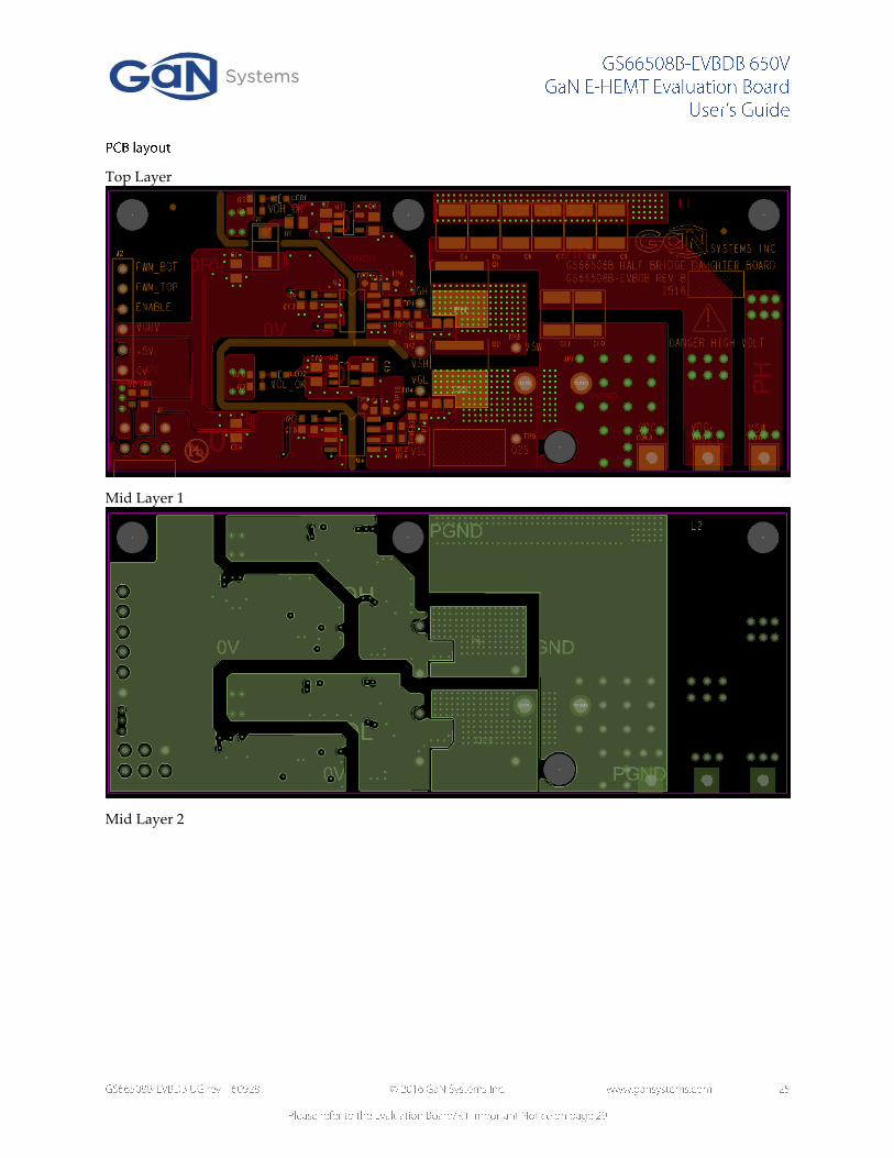
Top Layer
Mid Layer 1
Mid Layer 2
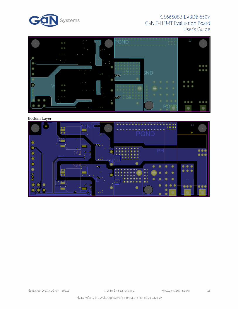
Bottom Layer

GS
66508B
HA
LF
BR
IDG
E D
AU
GH
TE
R C
AR
D 2016-0
6-1
0
BO
AR
D N
AM
E:
GS
66508B
-EV
BD
B
Re
vis
ion
B1
Last
Up
date
20160624
Qu
an
tity
Re
fere
nce
De
scri
pti
on
Valu
eM
an
ufa
ctu
rer
Part
nu
mb
er
Asse
mb
ly N
ote
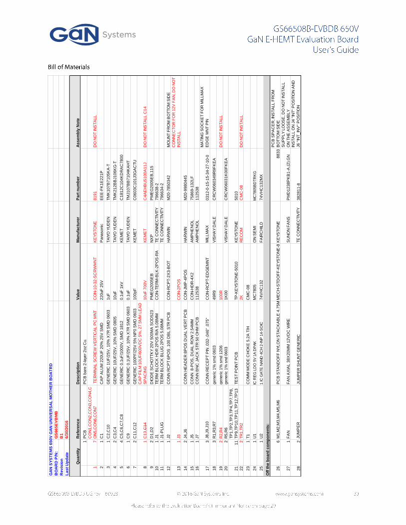
1P
CB
PC
B b
are
4-laye
r 2oz C
u.
13
CO
N1,C
ON
2,C
ON
3C
ON
N P
C P
IN E
DG
E M
NT
C
ON
-ED
GE
-MN
T-3
260M
ill-M
ax
3620-2
-32-1
5-0
0-0
0-0
8-0
matin
g r
ecepta
cle
on m
oth
er
board
:0312-0
-15-1
5-3
4-2
7-1
0-0
26
C1,C
2,C
3,C
14,C
15,C
16
CA
P, C
ER
, 4.7
UF
, 25V
, +
/-10%
, X
7R
, 0603
4.7
uF
TA
IYO
YU
DE
NT
MK
212A
B7475K
G-T
38
C4,C
5,C
6,C
7,C
8,C
9,C
10,C
11CA
P, C
ER
, 0.1
UF
,1K
V, +
/-10%
, X
7R
, 1812
0.1
uF
1kV
KE
ME
TC
1812C
104K
DR
AC
7800
44
C12,C
13,C
17,C
18
CA
P, C
ER
, 1U
F, 25V
, +
/-10%
, X
7R
, 0603
1uF
TA
IYO
YU
DE
NT
MK
107B
7105K
A-T
51
D1
DIO
DE
ULT
RA
FA
ST
600V
1A
SM
A600V
1A
FA
IRC
HIL
DE
S1J
For
boots
trap m
ode, D
O N
OT
INS
TA
LL
63
FB
1,F
B2,F
B3
0R
JU
MP
ER
0603
0R
generic 1
% 1
00ppm
0603
71
JP1
CU
RR
EN
T S
HU
NT
JU
MP
ER
CO
N-J
MP
-CS
HU
NT
--
For
curr
ent m
easure
ment, footp
rint
com
patib
le w
ith T
&M
SD
N-4
14-0
10
curr
ent shunt. U
se w
ide c
opper
foil
to
short
the c
onnectio
n if
not used for
better
81
J1C
ON
N 3
PIN
DU
AL R
OW
, 0.1
" P
ITC
H, R
/AC
ON
-HD
R-2
X3
HA
RW
IN IN
C.
M2
0-9
95
03
45
91
J2C
ON
-6P
OS
DO
NO
T IN
ST
ALL
10
2LE
D1,L
ED
2LE
D, G
RE
EN
, S
MD
0603
LE
D-S
MD
-0603
liteon
ltst-
c191kg
kt
11
2P
S1,P
S2
ISO
. D
C/D
C 5
-9V
, 1W
PE
S1-S
5-S
9-M
cui
PE
S1-S
5-S
9-M
12
2Q
1,Q
2G
aN
E-H
EM
T 6
50V
/30A
GS
66508B
GaN
Sys
tem
sG
S66508B
13
1R
1R
ES
,0 R
, 1%
, 0805
0R
For
boots
trap m
ode, D
O N
OT
INS
TA
LL
14
7R
2,R
3,R
4,R
8,R
9,R
10,R
13
RE
S, 3.3
K, 1%
,1/1
0W
, 0603
3.3
Kgeneric 1
% 1
00ppm
0603
15
4R
5,R
6,R
11,R
12
RE
S, 10R
, 1%
,1/1
0W
, 0603
10R
generic 1
% 1
00ppm
0603
16
2R
7,R
14
RE
S, 1R
, 1%
,1/1
0W
, 0603
1R
generic 1
% 1
00ppm
0603
17
6T
P1,T
P2,T
P3,T
P4,T
P5,T
P6P
robe test poin
tC
ON
-TP
-1P
OS
DO
NO
T IN
ST
ALL
18
4T
P7,T
P8,T
P9,T
P10
Pro
be test poin
tC
ON
-TP
-1P
OS
DO
NO
T IN
ST
ALL
19
2U
1,U
3R
EG
LD
O 6
V, 100m
A, S
TO
23-5
LP
2985IM
5-6
.1T
EX
AS
INS
TR
UM
EN
TS
LP
2985IM
5-6
.1/N
OP
B
20
2U
2,U
4IC
ISO
GA
TE
DR
IVE
R 2
.5K
V H
IGH
CM
TI
SI8
271G
B-IS
SIL
ICO
N L
AB
SS
I82
71
GB
-IS
Off
th
e b
oard
co
mp
on
en
ts:
21
1heats
ink,
35x3
5m
mx2
5.4
mm
, bla
ck
anodiz
ed
Cool I
nnova
tion
3-1
41
41
0U
BL
AN
DO
NO
T in
sta
ll o
n t
he
PC
B
asse
mb
ly, su
pp
ly lo
ose
wit
h p
re-
ap
plie
d T
he
rmal sh
ee
t (i
tem
#22)
22
1T
herm
al s
heet cut to
35x3
5m
m s
quare
berg
quis
tB
ON
D P
LY
100
Bo
nd
ply
100 t
he
rmal ad
he
siv
e
tap
e c
ut
to 3
5x35m
m a
nd
ap
ply
to
he
ats
ink s
urf
ace
(it
em
#21)
C1
4
10
uF
70
0V
FO
OTP
RIN
T F
OR
GS
665XX-E
VB
DB
M1
M2
M3
M4
PC
B S
TA
ND
OF
F 4
.75M
M M
NT H
OLE
KE
YS
TO
NE
8839-8
834
J1
1 2 VA
UX
_R
TN
U1 M
C7
80
5
IN1
OU
T3
GND4
C4
10u
C0
80
5
+5
VV
AU
X
0V
0V
CO
N2 1
CO
N61
EN
AB
LE
CO
N3 1
J5
12
34
5 76 8
0V
PW
M_
EXT
_H
PW
M_
INT
R6
1K
00
D1
PM
EG
20
05
EB
SO
D5
23
PW
M_
INT
_IN
V
TR
12K
C1
1100pF
0V
PW
M_
EXT
_L
PW
M_
INT
PW
M_
INT
_IN
V
VD
C-
R5
1K
00
C1
0
1uFC
9
0.1
uF
+5
V
J7
112538
1
2345
C1
3
10
uF
70
0V
R4
100R
R1
20
6
R2
100R
R1
20
6
U2
A
74
VH
C1
32
31 2
14 7
0V
R1
49
R9
0V
D2
PM
EG
20
05
EB
SO
D5
23
VD
C+
TR
22K
C1
2100pF
0V
U2
B
74
VH
C1
32
4 56
U2
C
74
VH
C1
32
9
10
8
U2
D
74
VH
C1
32
12
13
11
VD
C-
CO
N5 1
CO
N71
TP
3
TP
4
TP
1
TP
2
TP
7
+5
V
TP
8
0V
0V
VA
UX 1
2V
IN
EXTE
RN
AL P
WM
IN
PU
TTO
DS
P/M
CU
CO
NTR
OL B
OA
RD
PW
M IN
PU
T S
ELE
CTIO
N
ON
BO
AR
D D
EA
D T
IME
GE
NE
RA
TIO
N C
IRC
UIT
US
E T
R1 A
ND
TR
2 T
O A
DJU
ST D
EA
D T
IME
PO
S 2
/3:
IN
TE
RN
AL P
WM
SIG
NA
L
VO
UT
C1
22
0u
F 2
5V
CA
PA
L-P
AN
A-F
C2
1u
F 2
5V
VD
C_P
VD
C_N
VO
UT
+5V
VC
C
CO
N11
J31
1
22
TO
12V
FA
N
CO
N4 1
PO
S 1
: E
XT.
PW
M S
IGN
AL
DN
P
DN
P
DN
P
VS
W
TP
6
TP
9
TP
-KE
YS
TO
NE
-50
10
+5
V
PW
MH
_IN
TP
10
TP
-KE
YS
TO
NE
-50
10
TP
11
TP
-KE
YS
TO
NE
-50
10
TP
12
TP
-KE
YS
TO
NE
-50
10
TP
13
0V
+1
2V
PW
NL
_IN
PW
M
OU
TP
UT
INV
ER
TE
D
PW
M O
UTP
UT
VS
W
NO
TE
S -
UN
LE
SS
OTH
ER
WIS
E S
PE
CIF
IED
1.
ALL S
MD
RE
SIS
TO
RS
AN
D C
AP
AC
ITO
RS
AR
E 0
603 S
IZE
0V
0V
J2
12
34
56
J4
PO
S 4
: O
FF
C5
C6
T1
CM
C-0
8
14
23
J6
VD
RV
R3
49
R9
DN
PD
NP
+1
2V
R7
49
R9
C3
10u
C0
80
5
C7
C8
0.1
uF
1kV
C1
81
2V
DC
+
2.
DO
NO
T IN
STA
LL T
R1,T
R2,R
2,R
3 A
ND
C14
J8
1
J9
1
J1
01
TP
5
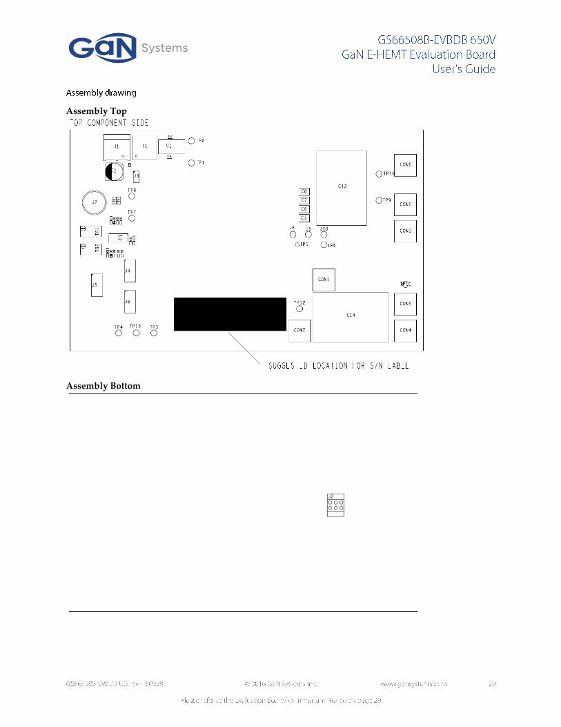
Assembly Top
Assembly Bottom
GA
N S
YS
TE
MS
65
0V
GA
N U
NIV
ER
SA
L M
OT
HE
R B
OA
TR
D
BO
AR
D P
/N:
GS
66
5E
VB
MB
Re
vis
ion
B1
La
st
Up
da
te6
/30
/20
16
Qu
an
tity
Re
fere
nc
eD
es
cri
pti
on
Va
lue
Ma
nu
fac
ture
rP
art
nu
mb
er
As
se
mb
ly N
ote
1P
CB
PC
B b
are
2-la
yer
2o
z C
u.
17
CO
N1
,CO
N2
,CO
N3
,CO
N4
,C
ON
5,C
ON
6,C
ON
7 T
ER
MIN
AL
SC
RE
W V
ER
TIC
AL
PC
MN
TC
ON
-10
-32
-SC
RW
MN
TK
EY
ST
ON
E8
19
1D
O N
OT
INS
TA
LL
21
C1
CA
P A
LU
M 2
20
UF
20
% 2
5V
SM
D
22
0uF
25
VP
ana
so
nic
EE
E-F
K1
E2
21
P
31
C2
,C1
0G
EN
ER
IC 1
UF
/25
V, 1
0%
X7
R S
MD
06
03
1uF
TA
IYO
YU
DE
NT
MK
10
7B
71
05
KA
-T
42
C3
,C4
GE
NE
RIC
10
UF
/25
V, 1
0%
SM
D 0
80
51
0uF
TA
IYO
YU
DE
NT
MK
21
2B
BJ1
06
KG
-T
54
C5
,C6
,C7
,C8
GE
NE
RIC
0.1
uF
/10
00
V, S
MD
18
12
0.1
uF
1kV
KE
ME
TC
18
12
C1
04
KD
RA
C7
80
0
61
C9
GE
NE
RIC
0.1
UF
/25
V, 1
0%
X7
R S
MD
06
03
0.1
uF
TA
IYO
YU
DE
NT
MJ1
07
BB
71
04
KA
HT
72
C1
1,C
12
GE
NE
RIC
10
0P
F/2
5V
5%
NP
0 S
MD
06
03
10
0p
FK
EM
ET
C0
60
3C
10
1J3
GA
CT
U
81
C1
3,C
14
CA
P F
ILM
10
UF
/60
0V
DC
5%
, 2
7.5
MM
LE
AD
SP
AC
ING
10
uF
70
0V
KE
ME
TC
4A
EH
BU
51
00
A1
1J
DO
NO
T IN
ST
AL
L C
14
92
D1
,D2
DIO
DE
SC
HO
TT
KY
20
V 5
00
MA
SO
D5
23
P
ME
G2
00
5E
BN
XP
PM
EG
20
05
EB
,11
5
10
1J1
TE
RM
BL
OC
K H
DR
2P
OS
R/A
5.0
8M
MC
ON
-TE
RM
-BL
K-2
PO
S-R
AT
E C
ON
NE
CT
IVIT
Y7
96
63
8-2
11
1J1
-PL
UG
TE
RM
BL
OC
K B
LU
G 2
PO
S 5
.08
MM
TE
CO
NN
EC
TIV
ITY
79
66
34
-2
12
1J2
CO
NN
RC
PT
6P
OS
.1
00
DB
L S
TR
PC
BC
ON
-RC
PT
-2X
3-B
OT
HA
RW
INM
20
-78
50
34
2M
OU
NT
FR
OM
BO
TT
OM
SID
E
13
1J3
CO
N-2
PO
S
CO
NN
EC
TO
R F
OR
12
V F
AN
, D
O N
OT
INS
TA
LL
14
2J4
,J6
CO
NN
HE
AD
ER
8P
OS
DU
AL
VE
RT
PC
B
CO
N-J
MP
-4P
OS
HA
RW
INM
20
-99
80
44
5
15
1J5
CO
NN
8
-PO
S, D
UA
L R
OW
2.5
4M
MC
ON
-HD
R-4
X2
AM
PH
EN
OL
75
86
9-1
32
LF
16
1J7
CO
NN
BN
C J
AC
K S
TR
50
OH
M P
CB
11
25
38
AM
PH
EN
OL
11
25
38
17
3J8
,J9
,J1
0C
ON
N R
EC
EP
T P
IN .0
32
-.0
46
" .0
75
"C
ON
-RC
PT
-ED
GE
MN
TM
ILL
MA
X0
31
2-0
-15
-15
-34
-27
-10
-0
MA
TIN
G S
OC
KE
T F
OR
MIL
LM
AX
ED
GE
MN
T P
IN
18
3R
1,R
3,R
7g
ene
ric 1
% s
md
06
03
49
R9
VIS
HA
Y D
AL
EC
RC
W0
60
34
9R
9F
KE
A
19
2R
2,R
4g
ene
ric 1
% s
md
12
06
10
0R
DO
NO
T IN
ST
AL
L
20
2R
5,R
6g
ene
ric 1
% s
nd
06
03
1K
00
VIS
HA
Y D
AL
EC
RC
W0
60
31
K0
0F
KE
A
21
11
TP
1,T
P2
,TP
3,T
P4
,TP
7,T
P8
,
TP
9,T
P1
0,T
P1
1,T
P1
2,T
P1
3T
ES
T P
OIN
T P
CB
TP
-KE
YS
TO
NE
-50
10
KE
YS
TO
NE
50
10
22
2T
R1
,TR
22
KR
EC
OM
CM
C-0
8D
O N
OT
INS
TA
LL
23
1T
1C
OM
M M
OD
E C
HO
KE
5.2
A T
/HC
MC
-08
24
1U
1IC
RE
G L
DO
5V
1A
DP
AK
MC
78
05
ON
SE
MI
MC
7805B
DT
RK
G
25
1U
21 IC
GA
TE
NA
ND
4C
H 2
-IN
P 1
4-S
OIC
74
VH
C1
32
FA
IRC
HIL
D7
4V
HC
13
2M
X
Off
th
e b
oa
rd c
om
po
ne
nts
:
26
6M
1,M
2,M
3,M
4,M
5,M
6P
CB
ST
AN
DO
FF
NY
LO
N S
TA
CK
AB
LE
4.7
5M
M H
OL
EM
EC
H-S
TD
OF
F-K
EY
ST
ON
E-8
83
0K
EY
ST
ON
E8
83
3
PC
B S
PA
CE
R, IN
ST
AL
L F
RO
M
BO
TT
OM
SID
E
27
1F
AN
FA
N A
XIA
L 3
8X
20
MM
12
VD
C W
IRE
S
UN
ON
FA
NS
PM
D1
23
8P
KB
1-A
.(2
).G
N
SU
PP
LY
LO
OS
E, D
O N
OT
INS
TA
LL
ON
TH
E A
SS
EM
BL
Y
28
2JU
MP
ER
JU
MP
ER
SH
UN
T G
EN
ER
ICT
E C
ON
NE
CT
IVIT
Y3
82
81
1-8
INS
TA
LL
ON
J4
"IN
T"
PO
SIT
ION
AN
D
J6
"IN
T_
INV
" P
OS
ITIO
N

GaN Systems Inc. (GaN Systems) provides the enclosed product(s) under the following AS IS conditions:
This evaluation board/kit being sold or provided by GaN Systems is intended for use for ENGINEERING
DEVELOPMENT, DEMONSTRATION, and OR EVALUATION PURPOSES ONLY and is not considered by GaN
Systems to be a finished end-product fit for general consumer use. As such, the goods being sold or provided are
not intended to be complete in terms of required design-, marketing-, and/or manufacturing-related protective
considerations, including but not limited to product safety and environmental measures typically found in end
products that incorporate such semiconductor components or circuit boards. This evaluation board/kit does not fall
within the scope of the European Union directives regarding electromagnetic compatibility, restricted substances
(RoHS), recycling (WEEE), FCC, CE or UL, and therefore may not meet the technical requirements of these directives,
or other related regulations.
If this evaluation board/kit does not meet the specifications indicated in the User’s Guide, the board/kit may be
returned within 30 days from the date of delivery for a full refund. THE FOREGOING WARRANTY IS THE
EXCLUSIVE WARRANTY MADE BY THE SELLER TO BUYER AND IS IN LIEU OF ALL OTHER WARRANTIES,
EXPRESSED, IMPLIED, OR STATUTORY, INCLUDING ANY WARRANTY OF MERCHANTABILITY OR FITNESS
FOR ANY PARTICULAR PURPOSE. EXCEPT TO THE EXTENT OF THIS INDEMNITY, NEITHER PARTY SHALL
BE LIABLE TO THE OTHER FOR ANY INDIRECT, SPECIAL, INCIDENTAL, OR CONSEQUENTIAL DAMAGES.
The user assumes all responsibility and liability for proper and safe handling of the goods. Further, the user
indemnifies GaN Systems from all claims arising from the handling or use of the goods. Due to the open construction
of the product, it is the user’s responsibility to take any and all appropriate precautions with regard to electrostatic
discharge.
No License is granted under any patent right or other intellectual property right of GaN Systems whatsoever. GaN
Systems assumes no liability for applications assistance, customer product design, software performance, or
infringement of patents or any other intellectual property rights of any kind.
GaN Systems currently services a variety of customers for products around the world, and therefore this
transaction is not exclusive.
Please read the User’s Guide and, specifically, the Warnings and Restrictions notice in the User’s Guide prior to
handling the product. Persons handling the product(s) must have electronics training and observe good
engineering practice standards.
This notice contains important safety information about temperatures and voltages. For further safety concerns,
please contact a GaN Systems’ application engineer.

Mouser Electronics
Authorized Distributor
Click to View Pricing, Inventory, Delivery & Lifecycle Information: GaN Systems:
GS66508B-EVBDB1