Embed Size (px)
Citation preview
scogna
interferencetechnology.com interference technology 1
emc design & software
A. CiCComAnCini SCognA, Ph. D cSt of America, inc. framingham, MA
AbStrACt
A physically based method is used for estimating the equivalent circuit model of an SMA connector soldered
on the top plane of a multi-layer board and connected to a single-end stripline. Starting from the scattering parameters (S-parame-ters) evaluated using a simulation software package, the equivalent circuit is extracted by modeling each part of the structure. The circuit is then validated by comparing the outputs obtained via circuit-level simula-tion of the extracted physical circuit with those computed by means of the full wave solution.
introDuCtionAt bit rates above one Gb/s, the effects of board discontinuities on the integrity of the signals cannot be ignored. For an accurate design, the effects of parasitic, packaging, board materials and trace geometries must be characterized and quantified. An essen-tial step in this process of characterization is the measurement of the properties of the board in terms of S-parameters, input im-pedance, noise voltage, etc.[1]
Microstrip and stripline structures cannot be connected directly to the co-axial ports of a network analyzer (NA). The structure or device-under-test (DUT) must be physically connected to the NA by some kind of transition network or fixture. One of the most frequently used fixtures or connec-
tors for this kind of application is the surface mounted assembly (SMA)[2] or simply the SMA connector.
The present paper proposes a Spice-like equivalent circuit of an SMA. Each part of the circuit is related to a single part of the connector, and the values of the pas-sive circuit elements are related to physical properties and dimensions of the SMA. It is worthwhile to note that the development of an equivalent circuit for the SMA requires less computational effort to achieve a solu-tion, and its use eliminates the necessity of performing repeated VNA calibrations[3–7] and/or de-embedding. In the next section, the SMA and the analyzed PCB configura-tion are described, and a physically-based circuit is proposed. Then, a full-wave software simulation[8] of the structure is performed, and the computed S-parameters are compared with those obtained by the equivalent circuit. Finally, some conclusions are addressed.
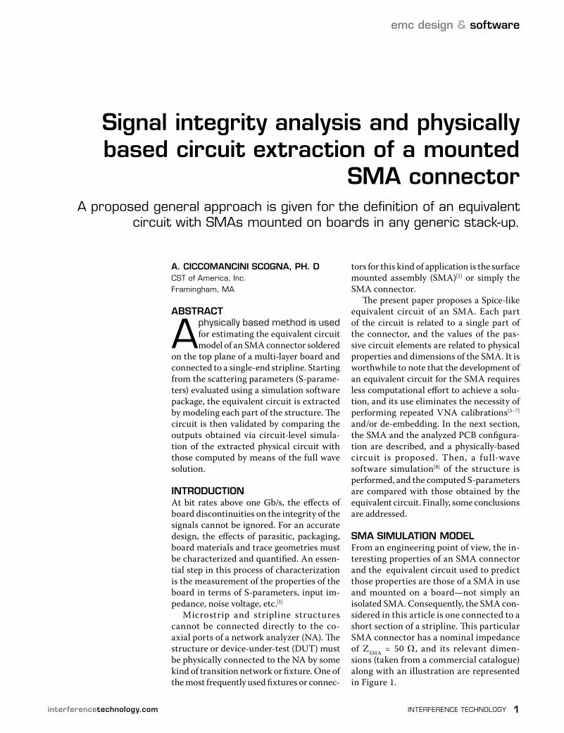
SmA SimulAtion moDelFrom an engineering point of view, the in-teresting properties of an SMA connector and the equivalent circuit used to predict those properties are those of a SMA in use and mounted on a board—not simply an isolated SMA. Consequently, the SMA con-sidered in this article is one connected to a short section of a stripline. This particular SMA connector has a nominal impedance of ZSMA = 50 Ω, and its relevant dimen-sions (taken from a commercial catalogue) along with an illustration are represented in Figure 1.
Signal integrity analysis and physically based circuit extraction of a mounted
SmA connectorA proposed general approach is given for the definition of an equivalent
circuit with SMAs mounted on boards in any generic stack-up.
2 interference technology eMc Directory & DeSign guiDe 2008
emc design & software analys is of a mounted sma connector
To characterize the electrical per-formances and to obtain an equivalent circuit of device behavior, a thorough description is need. This SMA is mounted on a multiple-layer board, and its central conductor is soldered in a through-hole via and is connected to a 2-cm long stripline (along the two inter-nal reference planes), with characteris-tic impedance o Zc = 50 Ω. Four lateral pins connect the external part of the SMA with the two reference planes. In the numerical electromagnetic model of the SMA, the conductive parts of the PCB are considered as copper (σ=5.8e7
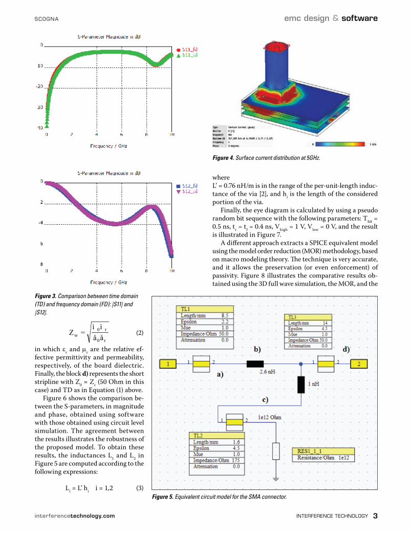
depicts the surface current distribution on the SMA connector, and it indicates how it is concentrated on the inner conductor pin, as well as around the lateral grounding pins.
Particular attention should be paid to excitation. The two “ports” at which the S-parameters are evaluated are the upper surface of the SMA and the end of the stripline. To ensure a TEM structure of the electromagnetic field (essential condition for a meaningful interpretation of the scattering ma-trix), lumped voltage sources should not be used because they would excite higher order modes. Because of this constraint, the TEM excitation has been obtained by examining waveguide ports that cause a TEM structure of the field at these planes. Simultaneously, it is a perfect match for the line imped-ance detected at the cross section.
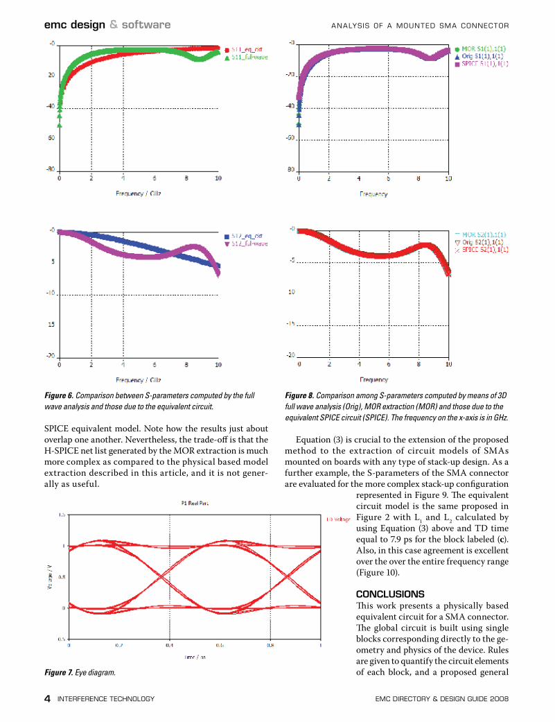
extrACtion of A PhySiCAl bASeD equivAlent CirCuitThe corresponding equivalent circuit is illustrated in Figure 5. The block la-beled a) is a lossless transmission line (TL) representing the upper external part (vis-à-vis the board) of the SMA. Its characteristic impedance Z0 is Z0 = ZSMA and its flight time is calculated by means of the following relation:
0
r ch
å=TD (1)
whereεr is the electric permittivity of the dielectric filling the connector, h is the height of the SMA’s external part, and c0 the speed of light.
The block labeled b) represents the inductance of the central pin from the top surface of the board to the stripline pad. At this point, the electromagnetic energy, in the form of voltage and cur-rent waves, is split into two parts; one flows along the stripline while the other continues through the via hole that acts as an open-end TL. Block c) represents the inductance of the remaining part of the via hole and its TL behavior. Because there is no clear reference conductor for this TL (vertically placed in respect to the reference planes), the characteristic impedance is taken equal to the wave impedance[9]
Figure 1. Real view of the SMA connector and 3D electromagnetic model.
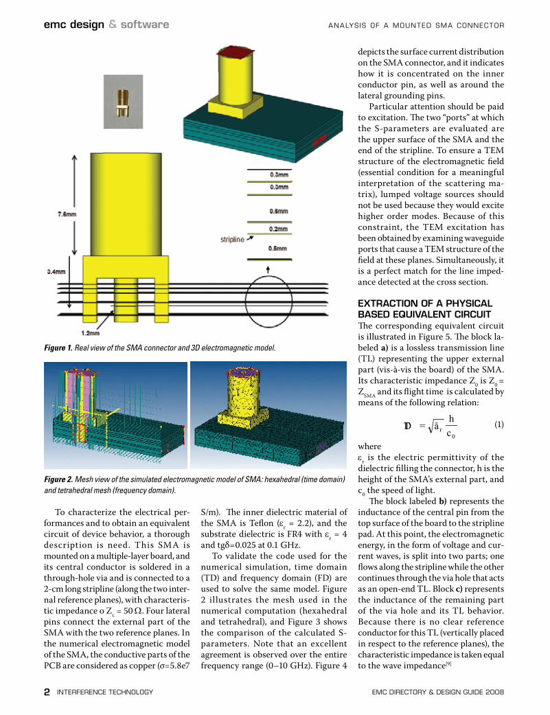
Figure 2. Mesh view of the simulated electromagnetic model of SMA: hexahedral (time domain) and tetrahedral mesh (frequency domain).
S/m). The inner dielectric material of the SMA is Teflon (εr = 2.2), and the substrate dielectric is FR4 with εr = 4 and tgδ=0.025 at 0.1 GHz.
To validate the code used for the numerical simulation, time domain (TD) and frequency domain (FD) are used to solve the same model. Figure 2 illustrates the mesh used in the numerical computation (hexahedral and tetrahedral), and Figure 3 shows the comparison of the calculated S-parameters. Note that an excellent agreement is observed over the entire frequency range (0–10 GHz). Figure 4
scogna
interferencetechnology.com interference technology 3
emc design & software
r0
r0w åå
ìì=Z (2)
in which εr and µr are the relative ef-fective permittivity and permeability, respectively, of the board dielectric. Finally, the block d) represents the short stripline with Z0 = Zc (50 Ohm in this case) and TD as in Equation (1) above.
Figure 6 shows the comparison be-tween the S-parameters, in magnitude and phase, obtained using software with those obtained using circuit level simulation. The agreement between the results illustrates the robustness of the proposed model. To obtain these results, the inductances L1 and L2 in Figure 5 are computed according to the following expressions:
Li = L’ hi i = 1,2 (3)
whereL’ = 0.76 nH/m is in the range of the per-unit-length induc-tance of the via [2], and hi is the length of the considered portion of the via.
Finally, the eye diagram is calculated by using a pseudo random bit sequence with the following parameters: Tbit = 0.5 ns, tr = tf = 0.4 ns, Vhigh = 1 V, Vlow = 0 V, and the result is illustrated in Figure 7.
A different approach extracts a SPICE equivalent model using the model order reduction (MOR) methodology, based on macro modeling theory. The technique is very accurate, and it allows the preservation (or even enforcement) of passivity. Figure 8 illustrates the comparative results ob-tained using the 3D full wave simulation, the MOR, and the
Figure 5. Equivalent circuit model for the SMA connector.
Figure 3. Comparison between time domain (TD) and frequency domain (FD): |S11| and |S12|.
Figure 4. Surface current distribution at 5GHz.♥
4 interference technology eMc Directory & DeSign guiDe 2008
emc design & software analys is of a mounted sma connector
SPICE equivalent model. Note how the results just about overlap one another. Nevertheless, the trade-off is that the H-SPICE net list generated by the MOR extraction is much more complex as compared to the physical based model extraction described in this article, and it is not gener-ally as useful.
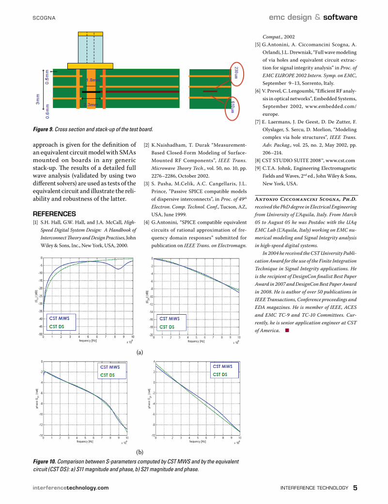
Equation (3) is crucial to the extension of the proposed method to the extraction of circuit models of SMAs mounted on boards with any type of stack-up design. As a further example, the S-parameters of the SMA connector are evaluated for the more complex stack-up configuration
represented in Figure 9. The equivalent circuit model is the same proposed in Figure 2 with L1 and L2 calculated by using Equation (3) above and TD time equal to 7.9 ps for the block labeled (c). Also, in this case agreement is excellent over the over the entire frequency range (Figure 10).
ConCluSionSThis work presents a physically based equivalent circuit for a SMA connector. The global circuit is built using single blocks corresponding directly to the ge-ometry and physics of the device. Rules are given to quantify the circuit elements of each block, and a proposed general
Figure 6. Comparison between S-parameters computed by the full wave analysis and those due to the equivalent circuit.
Figure 7. Eye diagram.
Figure 8. Comparison among S-parameters computed by means of 3D full wave analysis (Orig), MOR extraction (MOR) and those due to the equivalent SPICE circuit (SPICE). The frequency on the x-axis is in GHz.
scogna
interferencetechnology.com interference technology 5
emc design & software
approach is given for the definition of an equivalent circuit model with SMAs mounted on boards in any generic stack-up. The results of a detailed full wave analysis (validated by using two different solvers) are used as tests of the equivalent circuit and illustrate the reli-ability and robustness of the latter.
referenCeS[1] S.H. Hall, G.W. Hall, and J.A. McCall, High-
Speed Digital System Design: A Handbook of Interconnect Theory and Design Practises, John Wiley & Sons, Inc., New York, USA, 2000.
Figure 10. Comparison between S-parameters computed by CST MWS and by the equivalent circuit (CST DS): a) S11 magnitude and phase, b) S21 magnitude and phase.
Figure 9. Cross section and stack-up of the test board.
[2] K.Naishadham, T. Durak “Measurement-Based Closed-Form Modeling of Surface-Mounted RF Components”, IEEE Trans. Microwave Theory Tech., vol. 50, no. 10, pp. 2276–2286, October 2002.
[3] S. Pasha, M.Celik, A.C. Cangellaris, J.L. Prince, ”Passive SPICE compatible models of dispersive interconnects”, in Proc. of 49th Electron. Comp. Technol. Conf., Tucson, AZ, USA, June 1999.
[4] G.Antonini, “SPICE compatible equivalent circuits of rational approximation of fre-quency domain responses” submitted for publication on IEEE Trans. on Electromagn.
Compat., 2002[5] G.Antonini, A. Ciccomancini Scogna, A.
Orlandi, J.L. Drewniak, “Full wave modeling of via holes and equivalent circuit extrac-tion for signal integrity analysis” in Proc. of EMC EUROPE 2002 Intern. Symp. on EMC, September 9–13, Sorrento, Italy.
[6] V. Prevel, C. Lengoumbi, “Efficient RF analy-sis in optical networks”, Embedded Systems, September 2002, www.embedded.com/europe.
[7] E. Laermans, J. De Geest, D. De Zutter, F. Olyslager, S. Sercu, D. Morlion, “Modeling complex via hole structures”, IEEE Trans. Adv. Packag., vol. 25, no. 2, May 2002, pp. 206–214.
[8] CST STUDIO SUITE 2008™, www.cst.com[9] C.T.A. Johnk, Engineering Electromagnetic
Fields and Waves, 2nd ed., John Wiley & Sons, New York, USA.
Antonio Ciccomancini Scogna, Ph.D. received the PhD degree in Electrical Engineering from University of L’Aquila, Italy. From March 05 to August 05 he was Postdoc with the UAq EMC Lab (L’Aquila, Italy) working on EMC nu-merical modeling and Signal Integrity analysis in high-speed digital systems.
In 2004 he received the CST University Publi-cation Award for the use of the Finite Integration Technique in Signal Integrity applications. He is the recipient of DesignCon finalist Best Paper Award in 2007 and DesignCon Best Paper Award in 2008. He is author of over 50 publications in IEEE Transactions, Conference proceedings and EDA magazines. He is member of IEEE, ACES and EMC TC-9 and TC-10 Committees. Cur-rently, he is senior application engineer at CST of America. n
(b)
(a)