Embed Size (px)
Citation preview
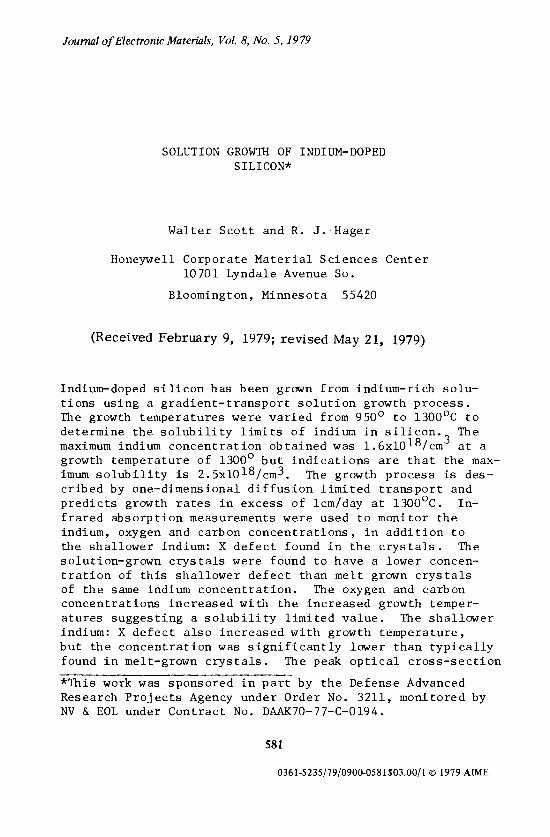
Journal o f Electronic Materials, Vol. 8, No. 5, 1979
SOLUTION GROWTH OF INDIUM-DOPED SILICON*
Walter Scott and R. J. Hager
Honeywell Corporate Material Sciences Center 10701 Lyndale Avenue So.
Bloomington, Minnesota 55420
(Received February 9, 1979; revised May 21, 1979)
Indium-doped silicon has been grown from indlum-rich solu- tions using a gradient-transport solution growth process. The growth temperatures were varied from 950 ~ to 1300~ to determine the solubility limits of indium in silicon. 3 The maximum indium concentration obtained was 1.6xl018/cm at a growth temperature of 1300 ~ but indications are that the max- imum solubility is 2.5x10¹⁸/cm 3. The growth process is des- cribed by one-dimensional diffusion limited transport and predicts growth rates in excess of icm/day at 1300~ In- frared absorption measurements were used to monitor the indium, oxygen and carbon concentrations, in addition to the shallower indium: X defect found in the crystals. The solution-grown crystals were found to have a lower concen- tration of this shallower defect than melt grown crystals of the same indium concentration. The oxygen and carbon concentrations increased with the increased growth temper- atures suggesting a solubility limited value. The shallower indium: X defect also increased with growth temperature, but the concentration was significantly lower than typically found in melt-grown crystals. The peak optical cross-section
*This work was sponsored in part by the Defense Advanced Research Projects Agency under Order No. 3211, monitored by NV & EOL under Contract No. DAAK70-77-C-0194.
581
0361-5235/79]0900-0581503.00/1 �9 1979 AIME
582 Scott and Hager
for indium was also determined to be 5.3x10⁻¹⁷cm 2 from
these measurements.
Key words: indium-doped silicon, solution growth, solubility, optical absorption.
Introduction
Indium-doped silicon is being investigated as an ex- trinsic photoconductor material for use in the 3 to 5 ~m infrared region. A number of problems have arisen with this material, notably with the low indium concentration obtained by standard growth methods and the presence of a shallower defect level associated with the indium. Czochralski grown crystals have been limited to a maximum indium concentration of 3.8x10¹⁷/cm j before microprecipitates are observed in the
( iv ~ crystals. The concentration of indium in float-zone grown crystals is generally even lower than this because of the low segregation coefficient of indium. (2) The limits to the in- dium solubility in silicon have not been previously reported in the literature to determine what improvement could be made in the doping levels in silicon crystals.
A shallower defect center associated with indium and labeled as indium:X has been observed in indium-doped silicon. Baron et al. (3) observed this defect in Hall coefficient measurements at an energy of about 0.ii eV. Subsequently, Scott (4) observed the infrared spectrum of an effective- mass-like defect associated with indium at an energy of 0.1128 eV. The origin of the defect is uncertain at this time, but it is known to exist in both Czochralski and float zone grown crystals.
Solution growth techniques such as gradient-transport solution growth and LPE have been used to grow III-V com- pounds for many years, but these techniques have not been extensively applied to silicon. Pfann (5) described the use of temperature-gradient zone melting as a means of producing large area p-n junctions in silicon, and more recently Cline and Anthony(6) have explored the migration of liquid metal droplets in silicon. An important feature of these solution growt h procedures is that the crystals are grown below the melting point of silicon, so the retrograde solubility of the impurities can be used to obtain very heavily doped crystals.
Solution Growth of Indium-Doped Silicon 583
In this paper we report the results of gradient- transport solution growth of silicon from indium solutions. The growths were done as a function of temperature to deter- mine the solubility limits of indium in silicon, Growth rates of about 4 mm/day have been achieved and crystals doped up to 1.6 x 10¹⁸/cm 3 with indium have been produced
by this technique. The growth rates agree with values com- puted from a one-dimensional diffusion model for the trans- port of silicon through indium.
We also report the results of infrared spectroscopic measurements on the solution grown crystals. A result of these measurements was a determination of the absorption cross-section for indium, which was 5.3 x lO-17cm 2. The absorption measurements were the primary means of evalu- ating the crystals to determine the effect of growth temper- ature on the concentration of the shallower defect in indium- doped silicon as well as to monitor the oxygen and carbon concentrations. The concentration of these shallower defects in the solution grown crystals is consistently lower than the concentration typically observed in melt-grown crystals with the same indium concentration.
Experimental Procedures
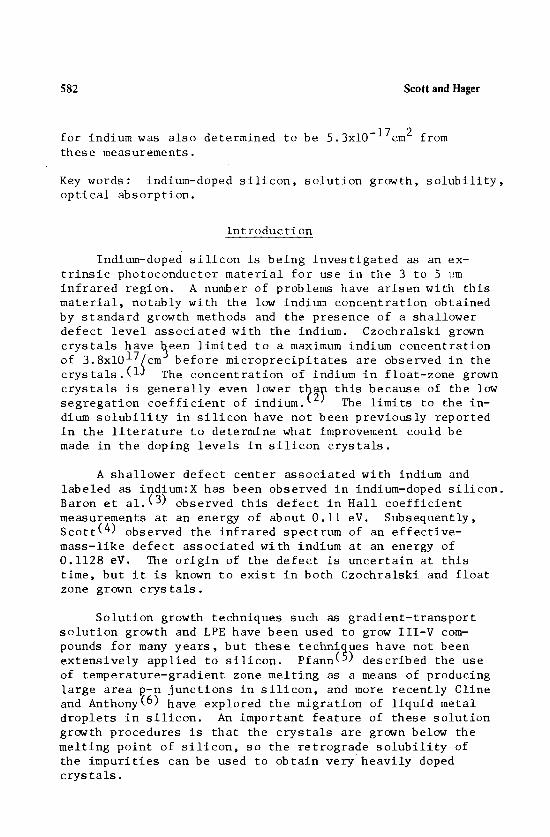
A schematic illustration of the growth apparatus used is shown in Figure i. It consists of a flat-bottomed quartz tube in which was placed a single crystal silicon seed, high purity (6N) indium, and a high purity silicon source in the relative positions shown in Figure i. A tubular quartz spacer was used to hold the siliconseed in place during the growth and prevent it from buoying to the surface of the liquid indium. ,The apparatus was placed in a furnace with uniform temperature profile and a temperature difference established between the silicon source and the substrate by a flow of air directed at the flat bottom of the ampoule. The temperature of the silicon seed is maintained approximately 50~ colder than the source temperature throughout the growth process.
The temperature difference between source and substrate was determined by calibrating the system using a Pt-Pt (3% Rh) thermocouple. The capsule was loaded with the usual amount of indium and a standard substrate. A quartz tube
584 Scott and Hager
T H
W o"
Ar
I I1, Quortz Amgoute
Quor tz SI~3cer
Si Source
tn
- - Si Seed
Cooling Air
Fig. 1 Schematic of the solution- growth apparatus.
containing the thermocouple was inserted into the indium to be in contact with the substrate. The apparatus was
brought up to temperature, and the temperature profile in the indium measured. The profile was measured with the gas flow rate a parameter in order to be able to set any desired temperature difference across the indium column. The repeatability of the temperature setting was estimated at about • 5~ from these calibration measurements.
The carrier concentration was determined from Hall measurements made in a dc mode at a field of 8KG with the samples in a bridge configuration. The contact was eva- porated aluminum annealed at 750~ fo~ 45 min. in hydrogen.
Solution Growth of Indium-Doped Silicon 585
Contact to the aluminum was made with ultra-sonically sol- dered indium.
Optical measurements were made using a Digilab F$S-14 Fourier transform spectrometer at a resolution of 2 ~7# and converted to absorption coefficient in the usual way. The samples were cut from the single crystal regions of the solution grown material, lapped and polished with a one-half degree taper to eliminate fringing, and were cooled to 8K for measurement. The silicon lattice absorption lines were subtracted from the spectra of the doped crystals to display the defect lines. The reference sample was a high purity vacuum float-zoned crystal which did not have impurity ab- sorption lines. The absorption spectrum of the high purity crystal was also measured at 8K to give complete subtraction of the lattice lines.
Gradient Transport Solution Growth
The fundamental process leading to growth of indium- doped silicon using the gradient-transport process has been described earlier by Pfann. (5) The process relies on an increase in solubility of the solute (silicon) with increas- ing temperature. Establishing a temperature gradient across the solvent (indium) generates a concentration gradient which leads to mass transport to the low temperature end.
The transport of silicon to the substrate is governed by the usual diffusion equation
$2Csi = DV2Csi 2 ' (i)
~t
where C S$ is the concentration of silicon in the melt in moles/ca 3 and D is the diffusion coefficient in the melt.
The boundary conditions are:
Csi(x,t ) = C o at x = 0 (source)
Csi(x,t) = C% at x = % (substrate)
Csi(X,O) = 0 initially .

586 Scott and Hager
In this form we have assumed the origin to be at the source, an indium column of length %, and no silicon in the melt to begin with. In addition, we have assumed the problem to be one-dimensional and that there are no edge effects due to the finite size of the source, substrate, and quartz apparatus. We also assume that the source and s ubstrate surfaces remain fixed relative to each other during the growth, which is not strictly true in the pro- cedure we use.
The solution to equation (i) is:
x CSi (x't) = Co- (Co-C~) 7 + (2)
C~c~ ~ sin m~x -m2~2Dt 1 m ~ exp ~2
Except for small times only the first term in equation (2) is important so it can be approximated by:
x
Csi(X,t) = Co - (Co-C%) 7-
.vx e - y 2~ (Co+C%) sin -~- (3)
2Dt where y = ~2
E x a m i n i n g e q u a t i o n (4) i t i s c l e a r t h a t f o r l o n g t i m e s t h e c o n c e n t r a t i o n a p p r o a c h e s a l i n e a r v a r i a t i o n w i t h x , i . e .
x C(x,=) = C - (Co-C ~) -~ , (4)
o
which is expected in the steady state.
~qe crystal begins growin~ on the substrate when the mass transport is in the direction of the substrate every- where in the ampoule; i.e., when
dCsi
dx --- < 0 at x = ~.
Solution Growth of Indium-Doped Silicon 587
This condition is satisfied when
C - Cg -y = o
e 2(Co+C~)
The time before indium-doped silicon starts to grow on the substrate is:
~2 C O - C%
t G = - ~ gn 2(Co+C~) (5)
The time turns out to be in the range 5.7 - 5.9 hours for temperatures up to 1200~ By 1300~ this time drops to about 3.2 hours. As a result, this initial transient is only a small portion of the growth time, which was typically 5 to i0 days.
The growth rate can be computed from equation (2) and the condition
3Csi J =-D ~ x lx = E '
where J is the particle current in molesLcm2sec, and CSi is the silicon collcentration in moles/cm j. The growth rate at the substrate is miven by
MSi V (cm/sec) = J - , (3)
PSi
where MSi is the molar weight of silicon, and Si is the density of the silicon crystal. Using equation (3) the steady state growth rate can be written
MSi (Co-C E) V (cm/sec) = D-- (4)
PSi
The steady state growth rate therefore depends on the concentration gradient in the indium and the diffusion rate of silicon through the indium.
588 Scottand Hager
To characterize the growth process completely, we need to know only two parameters:
(a) the diffusion coefficient, D, and
(b) the Si-In ]iquidus.
The diffusion coefficient in liquid indium has been measured up to a temperature of 1000~ and is given by the expression
D = 3 x 10 -4 exp - 2.5 kcal/mole cm2/sec RT
where R is the gas constant. The Si-In liquidus values ~qed were obtained from the data of Thurmond and Kowalchik.(9)
The predicted growth rate in units of mm/day is shown in Figure 2 as a function of the growth temperature. For a given temperature gradient, the growth rate increases dramatically with increasing growth temperature up to about 1300~ because of the increased solubility of silicon in indium at the higher temperature. The slope of the liquidus dC d-T ' has a maximum near 1300~ accounting for the maximum
in growth rate. The maximum rate is expected to be in the 10-20 mm/day range under these growth conditions. The experimentally measured growth rates are also shown in Figure 2 and are discussed in the next section.
Results and Discussion
Crystal Growth
Crystals have been grown at temperatures ranging from about 950~ to 1300~ Typicaily, the solution-grown material was single crystal in the vicinity of the ori- ginal substrate, indicating epitaxial growth had occurred. This single crystal portion was in the range of 2 to 7 mm in length. The remaining indium-doped material was poly- crystalline, occasionally containing some indium inclusions. The over-all length of the crystals ranged from about 5 mm to 1.7 cm.
A problem encountered with this growth method was in obtaining uniform wetting of the substrate and having melt- back occur across the entire face of the substrate. This

Solution Growth of Indium-Doped Silicon 589
10 )-
E E
~_ 1 .0
0
O.I 900
IT Z ~ X x I I
I I I I ; I I IOOO IO50 I100 I 150 12OO 12~O 13OO I ] 5 0
GROWTH TEMPERATURE (raG)
Fig. 2 Growth rates for diffusion through a 3cm solumn of Lndium with a 50~ temperature difference from source to substrate. ~e solid line is calculated from a one-dimensional diffusion model.
was particularly serious at growth temperatures below about I050~ At the higher temperatures, this was much less of a problem and uniform wetting was generally ob- served across the entire substrate surface.
The measured growth rates are shown in Figure 2. In general the measured values agree very well with calculated values, indicating that reasonable values of the parameters were used in the calculation. The errors assigned to the growth rates result from an uncertainty in the degree of melt-back of the substrate and also from an uncertainty in the amount of growth. On cool-down, material would pre- cipitate on the solution'grown crystal giving an uncertainty as to the length of the crystal. Some error also occurs in determining the length of time of the growth, since it requires some time for steady state to be reached. The growths were typically about i0 days, so this is judged to be only a small error. This uncertainty in growth rate is typically _+ 20%, so still provides a sufficiently accurate comparison with the simple one dimensional diffusion model.
590 Scott and Hager
The growth rates at 1250~ and 1300~ are below the values calculated for a 3cm indium column. At the equi- valent source temperatures of 1300~ and 1350~ respectively, the solubility of silicon in the indium becomes very large, which means that the total liquid column between the source and the substrate will be greater than the 3cm used in the calculation. As an example, at a source temperature of 1350~ the equilibrium concentration of silicon in solution is 0.8 atom fraction. If the entire column were at that temperature, then the liquid would occupy a length of about 12cm, rather than the 3cm we assumed. Correcting for this change in liquid length would bring the calculated growth rates more in line with measurements.
Crystal Evaluation
Electrical Evaluation. All the crystals were character- ized by Hall coefficient versus temperature measurements on at least one sample from each growth taken from the single crystal portion of the growth. A major problem in the electrical transport measurements of deep impurities in silicon is in determining the total concentration of the impurities. Hall measurements provide a measure of the free carrier concentration, but if all the impurities are not ion- ized at the temperature of measurement then a specific model must be adopted before the total impurity concentration can be determined.
The free carrier concentration, p, was determined from the Hall coefficient, RH, from the expression
r P eR H
where the scattering factor, r, was assumed to be unity. The carrier concentration is also determined from the charge neutrality condition
+ =NA , P +N D +
where N D is the concentration of ionized donors, and NA is the concentration of ionized acceptors. By assuming a low concentration of compensating donors and a high con- centration of indium relative to any other acceptor, this can be rewritten as

Solution Growth of Indium-Doped Silicon 591
p = Nln
Ei-E F 1 + g exp KT
(5)
where Nin is the total In concentration, g is the ground state degeneracy, E i is the In ionization energy, and Ey is the Fermi energy. In this expression the effects of the indium excited states have been ignored, and only the ground state considered.
The hole concentration is also determined from the usual e x p r e s s i o n f o r n o n - d e g e n e r a t e b a n d s
N v
P = EF (6)
I + exp ~-~
where N v i s t h e e f f e c t i v e d e n s i t y o f s t a t e s i n t h e v a l a n c e b an d.
Combining equation (5) and (6) gives the hole concen- tration as a function of the total indium concentration.
The values of the various parameters used in the calcu- lation were the following:
N v = 4.8296 x 10¹⁵ (m'h/moT)3/2
m* h = 0.81 at 300K (lO)
E i = 0.155 eV
g = 4
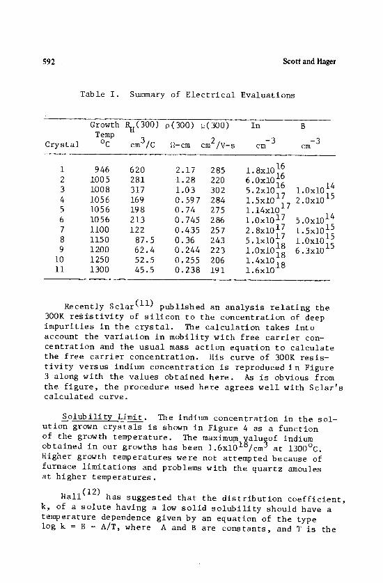
A summary of the properties of the various crystals is presented in Table I. The 300K electrical properties are listed along with the growth temperature and the calculated indium concentration. The boron concentration observed in the crystals is also listed in Table I, and was obtained from the exhaustion plateau observed in the Hall coeffic- ient verses reciprocal temperature plot. The cases where no boron concentration is listed are those where the Hall coefficient versus reciprocal temperature curve did not have a boron exhaustion plateau.
592 Scott and Hager
Table I. Summary of Electrical Evaluations
Crystal
Growth ~(300) p(300) p(300) In
Temp - 3 ~ cm3/C ~-cm cm2/V-s cm
B
-3 cm
1 2 3 4 5 6 7 8 9
i0 ii
946 620 2.17 285 1005 281 i.28 220 1008 317 1.03 302 1056 169 0.597 284 1056 198 0.74 275 1056 213 0. 745 286 ii00 122 0.435 257 1150 87.5 0.36 243 1200 62.4 0.244 223 1250 52.5 0.255 206 1300 45.5 0.238 191
i. 8x10¹⁶ 16
6.0xl0 ~. 5.2xi0 • l.OxlO 14 1.5x10¹⁷_ 2.0x10 15 i. 14xlO i ! 1.0xl017 5.0x10¹⁴ 2.8xi017 [ 15 5x10 5 ixl017 " 15 �9 18 1.0xl0
l.Oxl0~ 6.3xi015
1.4x10 ~ ̂ 1.6x10 •
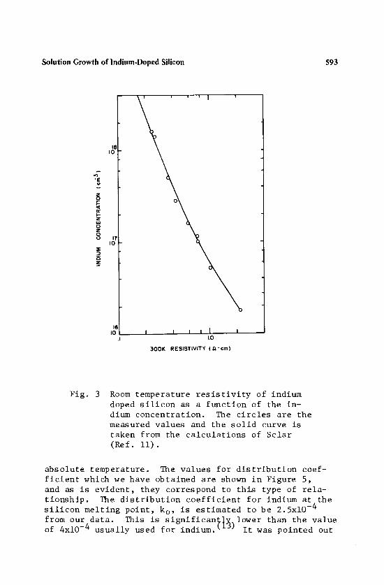
Recently Sclar (II) published an analysis relating the 300K resistivity of silicon to the concentration of deep impurities in the crystal. The calculation takes into account the variation in mobility with free carrier con- centration and the usual mass action equation to calculate the free carrier concentration. Ills curve of 300K resis- tivity versus indium concentration is reproduced in Figure 3 along with the values obtained here. As is obvious from the figure, the procedure used here agrees well with Sclar's calculated curve.
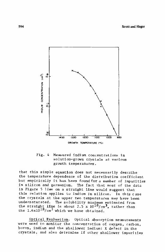
Solubility Limit. The indium concentration in the sol- ution grown crystals is shown in Figure 4 as a function of the growth temperature. The maximum valueof indium obtained in our growths has been ].6x1018/cm3 at 1300~ Higher growth temperatures were not attempted because of furnace limitations and problems with the quartz amoules at higher temperatures.
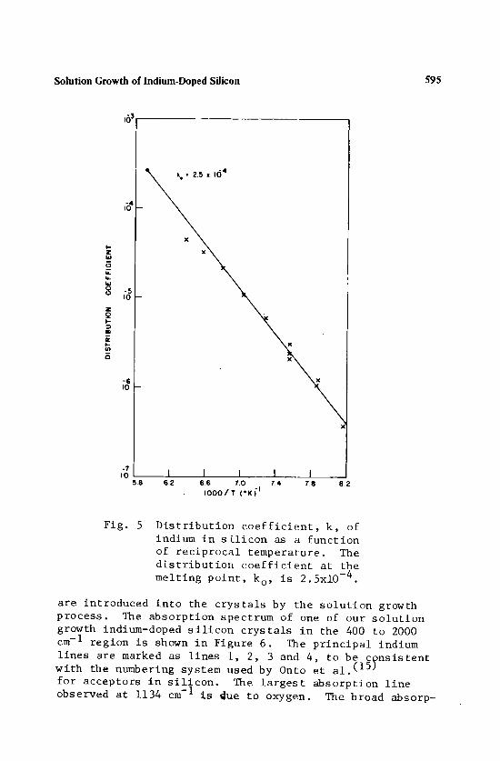
Hall (12) has suggested that the distribution coefficient, k, of a solute having a low solid solubility should have a temperature dependence given by an equation of the type log k -- B - A/T, where A and B are constants, and T is the
Solution Growth of Indium-Doped Silicon 593
o
I.-
z 0
~5 _z
16 I 0 I I i i I I
i.O
300K RESiSTiViTY (n-cm)
Fig. 3 Room temperature resistivity of indium doped silicon as a function of the in- dium concentration. The circles are the measured values and the solid curve is taken from the calculations of Sclar (Ref. Ii).
absolute temperature. The values for distribution coef- ficient which we have obtained are shown in Figure 5, and as is evident, they correspond to this type of rela- tionship. The distribution coefficient for indium at the silicon melting point, ko, is estimated to be 2.5xi0 -4 from our data. This is significantlv lower than the value of 4x10 -4 usually used for indium.(13) It was pointed out
594 Scott and Hager
~ g u
z
w
z
,6[ IOi
x \
|
,~oo ,,% ,~o tlO0 iO00 900
GROWTH TEMPERATURE ( 'C |
Fig. 4 Measured indium concentrations in solution-grown crystals at various growth temperatures.
that this simple equation does not necessarily describe the temperature dependence of the distribution coefficient but empirically it has been found for a number of impurities in silicon and germanium. The fact that most of the data in Figure 5 lies on a straight line would suggest that this relation applies to indium Jn silicon. In this case the crystals at the upper two temperatures may have been undersaturated. The solubility maximum estimated from the straight llne is about 2.5 x 10¹⁸/cm3, rather than the 1.6xl018/cm 3 which we have obtained.
Optical Evaluatio__n_n. Optical absorption measurements were used to monitor the concentration of oxygen, carbon, boron, indium and the shallower indium: X defect in the crystals, and also determine if other shallower impurities
Solution Growth of Indium-Doped Silicon 595
Z
a
- 7 tO I I I I I
5.8 s.2 s.s T.O 7.4 7.8 o 2 t O O O / T ( ' K ) "t
Fig. 5 Distribution coefficient, k, of indium in sLlicon as a function of reciprocal temperature. The dLstribution coefficient at the melting point, ko, is 2.5xi0 -4.
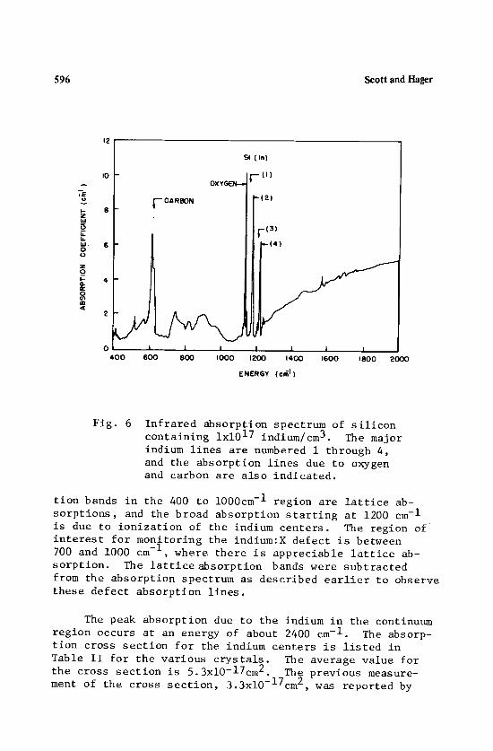
are introduced into the crystals by the solution growth process. The absorption spectrum of one of our solution growth indium-doped silicon crystals in the 400 to 2000 cm -I region is shown in Figure 6. The principal indium lines are marked as lines i, 2, 3 and 4, to be consistent with the numbering system used by Onto et al. (]5) for acceptors in silicon. The largest absorption line observed at 1134 cm -I is due to oxygen. The broad absorp-
596 Scott and Hager
w
o
I0
vl'-- CA RBON
0 i 1 I 4 0 0 6O0 800 I 0 0 0
Si ( In}
- - ( t ) OXYC.~N--
~ ( 2 )
iv(3) ~ ( 4 )
1 I | 1200 1400 1600
ENERGY (cn~ I )
I 1800 2000
Fig. 6 Infrared absorption spectrum of silicon containing ixl017 indium/cm 3. The major indium lines are numbered 1 through 4, and the absorption lines due to oxygen and carbon are also indicated.
tion bands in the 400 to 1000cm -I region are lattice ab- sorptions, and the broad absorption starting at 1200 cm -I is due to ionization of the indium centers. The region of interest for monitoring the indium:X defect is between 700 and I000 cm -I, where there is appreciable lattice ab- sorption. The lattice absorption bands were subtracted from the absorption spectrum as described earlier to observe these defect absorption lines.
The peak absorption due to the indium in the continuum region occurs at an energy of about 2400 cm -I. The absorp- tion cross section for the indium centers is listed in Table II for the various crystals. The average value for
the cross section s~S ~ ~xl031~Cl~ cThm~,pr=iOUp mtadUb; �9 ~ ~ ~
ment of the cross c i -17 o

Solution Growth of Indium-Doped Silicon 597
Table II. Absorption Cross Section of Indium
peak Crystal # (cm -I) ~
3 3.01 5.54 4 7.6 5.07xi0 -17
6 7.2 7.2 7 15 5.35 8 26 5.09 9 42.5 4.25
i0 67 4.78 ii 82 5.13
Average o = 5.30x10⁻¹⁷cm 2 opt
Messenger and Blakemore (16) In their interpretation they used a value of 6 for the indium ground state degeneracy, which would tend to overestimate the indium concentration in their crystals. Using a degeneracy of 4 brings their cross section in line with the value we observe.
The shallower indium:X defect was previously shown to have an effective-mass like absorption spectrum with the principal absorption lines at 800cm -I, 830cm -I and 873cm-] (4). The integrated intensity of the strongest line at 830cm -I was used to determine the concentration of this defect. To convert the optical absorption measurement to carrier concentration, the integrated cross section for this llne had to be estimated. This was done in the follow- ing way: First, the integrated cross section for this transition was measured in crystals doped with the Group IIIA acceptors boron, alumisum and indium. These cross- sections were 6.5 -+ 1.5xlO-14cm -I in boron, 2.5 _+ 0.5x10 -14 cm -I in aluminum, and 4.5 -+ 1.0xl0 -16 in indium. Plotting the logarithm of cross section versus impurity ionization energy produced a straight line for these three acceptors. According to this plot, defect at 0.1128 eV should have an integrated cross section of 3.5 -+ 0.5xlO-15cm.
598 Scott and Hager
1016
8
==
i x 14
A BA~IN et Qt. /"t Oz & FZ ~ l +
0
�9 ~
O SOLUTION GROWN
& Gz
i~) 3 i , I i i i i I
i017 i O 18
INDIUM GONG. ( cm 3)
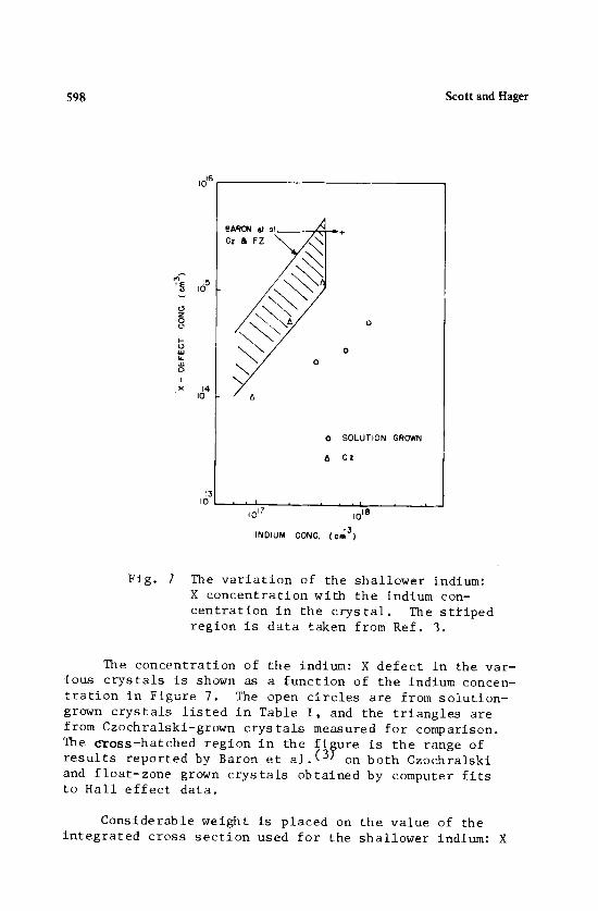
Fig. 7 The variation of the shallower indium: X concentration with the indium con- centration in the crystal. The striped region is data taken from Ref. 3.
The concentration of the indium: X defect in the var- ious crystals is shown as a function of the indium concen- tration in Figure 7. The open circles are from solution- grown crystals listed in Table I, and the triangles are from Czochralski-grown crystals measured for comparison. The r region in the figure is the range of results reported by Baron et al. (37 on both Czochralski and float-zone grown crystals obtained by computer fits to Hall effect data.
Considerable weight is placed on the value of the integrated cross section used for the shallower indium: X
Solution Growth of Indium-Doped Silicon 599
defect in determining the defect concentration. If this value is incorrect, then the points shown in Figure 7 are correspondingly incorrect. The fact that the indium: X concentration obtained in Czochralski crystals falls in
(3) �9 �9 the same range obtained by Baron et al. indlcates that the optical measurements are at least consistent with the electrical transport measurements.
A more important factor to consider, however, is the precision of the optical measurements. Typically this is about • 20% in doping level, with a minimum sensitivity limit of about 5xlOl3/cm 3 for the indium:
X defect. As a result, the relative values obtained by optical absorption should be representative of the difference between Czochralski and solution-grown crystals. For a given indium concentration, the indium: X concentra- tion in the solution-grown crystals is about a factor of five lower than in Czochralski-grown crystals.
As an example, we were able to measure the indium: X concentration in both a Czochralski-grown crystal and a solution-grown crystal with an indium concentration of 3.8x i017/cm3. The Czochralski crystal contained 1.3xl015/cm 3 of the indium: X defect, while the solution grown crystal contained 2xl014/cm 3 of the defect.
The concentrations of both oxygen and carbon were measured in the crystals as a measure of crystal purity. The oxygen concentration was determined from the peak intensity of the i134cm -I line at 8K, and the carbon con- centration was determined from the intensity of the 606cm -I llne. The conversion from peak absorption coefficient to doping level taken from the literature using the room temperature values reported by Gaff et ai.(17) for oxygen and by Newman and Willis(18) for carbon. The absorption coefficient for these lines was measured as a function of temperature to determine the appropriate conversion at 8K. Thelvalues used for the 8K measurements were 3.1x10¹⁶/cm3/ cm- for oxygen, and 6.7xl016/cm3/cm -I for carbon.
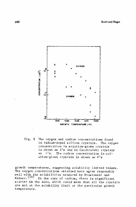
The oxygen and carbon concentrations are shown in Figure 8 as a function of the growth temperature. The oxygen concentrations of four Czochralski grown crystals are also shown in Figure 8 for comparison. Both the oxygen and carbon concentrations increase with increasing
600 Scott and Hager
'5
re I - ..=, o
oo
x OXYGEN
x
x
x
x
o o
o CARBON o
o
o
l I l l t4OO t30O 1200 t tO0
GROWTH T E M P E R A T U R E ( ' C )
x
o
I iooo
Fig. 8 The oxygen and carbon concentrations found in indium-doped silicon crystals. The oxygen concentration in solution-grown crystals is shown as X's and in Czochralski crystals as A's. The carbon concentration in sol- ution-grown crystals is shown as O's
growth temperatures, suggesting solubility limited values. The oxygen concentrations obtained here agree reasonably well with the solubilities measured by Hrostowski and Kaiser. (19) In the case of carbon, there is significant scatter in the data, which could mean that all the crystals are not at the solubility limit at the particular growth temperature.
Solution Growth of Indium-Doped Silicon 601
Summary
We have demonstrated that indium-doped silicon, doped at the solubility limits of indium, can be grown from an indium solution using the gradient-transport solution growth process. Growth rates of 4mm/day have been obtained making the technique feasible as a method of producing heavily doped silicon wafers in low volume applications. The solubility limit of indium has, for the first time, been measured over the 950 ~ to 1300~ temperature range. The maximum solubility obtained in the solution-grown crystals was 1.6xlOl8cm 3, but the indications are that the maximum solubility occurs at about 1300~ with a value of about 2.5x10¹⁸/cm 3. Optical absorp- tion measurements have verified that the concentration of the shallower indium: X defect is lower in the solution grown crystals than in the conventionally grown crystals reported in the literature. The optical absorption measure- ments also provided a measurement of the indium optical absorption ~ross section. This was determined to be 5.3x10⁻¹⁷cm �9
Acknowledgements
The authors would like to acknowledge the assistance of J. E. Sjerven making the optical measurements and J. L. Schmit for many helpful discussions.
References
i. E. L. Kern, R. Baron, R. H. Walker, D. J. O'Connor and O. J. Marsh, J. Electron. Mater. 4, 1249 (1975)
2. W. R. Runyan, "Silicon Semiconductor Technology", (McGraw Hill, New York, 1965).
3. R. Baron, M. H. Young, J. K. Neeland, and O. J. Marsh, Appl. Phys. Lett. 30, 594 (1977)
4. W. Scott, Appl. Phys. Lett. 32, 540, (1978).
5. W. G. Pfann, "Solid State Physics" Volume 4, F. Seitz and D. Turnbull, editors. (Academic Press, N.Y., 1957) pp. 424.
602 Scott and Hager
References Cont'd
6. H. E. Cline and T. R. Anthony, J. Appl. Phys. 48, 2196, (1977), and the references therin.
7. T. S. Moss, "Optical Properties of Semiconductors" (Academic Press, New York 1959), P 14.
8. The data for diffusion in liquids is summarized in: N. H. Nachtreib, Adv. Phys. ]6, 309 (1967).
9. C. D. Thurmond and M. Kowalchlck, Bell Syst Tech. J. 39, 169, (1960)
i0. H. D. Barber, Solid State Elect. lO, 1039 (1967).
ii. N. Sclar, IEEE Trans. El. Dev. ED-24,709 (1977).
12. R. N. Hall, J. Phys. Chem. Solids 3, 63 (1957).
13. F. A. Trumbore. Bell. Svst. Tech. J. 39, 205 (]960).
14. F. A. Trumbore, C. R. Isenberg, and E. M. Porbansky, J. Phys. Chem. Solids 9, 60 (1958).
]5. A. Onton, P. Fisher, A. K. Ramdas, Phys. Rev. 163, 686, (1967).
16. R.A. Messenger and J. S.Blakemore, Solid State Commun. 9, 319, (1971).
17. K. Graff, E. Grallath, S. Ades, G. Goldback and G. Tolg, Solid State Electron. 16, 887 (1973).
18. R. C. Newman and J. B. Willis. J. Phys. Chem. Solids 26, 373 (1965).
19. H. J. Hrostowski and R. H. Kaiser, Phys. Rev. 107, 969 (1957).