Embed Size (px)
Citation preview

EE130 Lecture 42, Slide 1 Spring 2007
Lecture #42
OUTLINE • IC technology• MOSFET fabrication process• CMOS latch-up
Reading: Chapter 4
Die photo of Intel Penryn processor(Intel®CoreTM2 family)
courtesy of Chipworks
Cross-sectional SEM view ofAMD Athlon 64 x2 processor
Note: HW#14 was updated this morning. (There are only 4 problems!)
EE130 Lecture 42, Slide 2 Spring 2007
“Planar” fabrication process:
Simultaneous fabrication of many “chips” on a wafer, each comprising an integrated circuit (e.g. a microprocessor or memory chip) containing millions or billions of transistors
Method:
Sequentially lay down and pattern thin films of semiconductors, metals and insulators.
Materials used in a basic CMOS integrated circuit:• Si substrate – selectively doped in various regions• SiO2 insulator• Polycrystalline silicon – used for the gate electrodes• Metal contacts and wiring
300mm Si wafer
Integrated Circuit Technology

EE130 Lecture 42, Slide 3 Spring 2007
Formation of Insulating Films
• The favored insulator is pure silicon dioxide (SiO2).
• A SiO2 film can be formed by one of two methods:
1. Oxidation of Si at high temperature in O2 or steam ambient
2. Deposition of a silicon dioxide film
ASM A412batchoxidationfurnace
Applied Materials low-pressure chemical-vapor deposition (CVD) chamber

EE130 Lecture 42, Slide 4 Spring 2007
Patterning the Layers
Lithography refers to the process of transferring a pattern to the surface of the waferEquipment, materials, and processes needed:• A mask (for each layer to be patterned) with the desired pattern
• A light-sensitive material (called photoresist) covering the wafer so as to receive the pattern
• A light source and method of projecting the image of the mask onto the photoresist (“printer” or “projection stepper” or “projection scanner”)
• A method of “developing” the photoresist, that is selectively removing it from the regions where it was exposed
Planar processing consists of a sequence of additive and subtractive steps with lateral patterning
oxidationdeposition
ion implantation
etching lithography

EE130 Lecture 42, Slide 5 Spring 2007
In order to transfer the photoresist pattern to an underlying film, we need a “subtractive” process that removes the film, ideally with minimal change in the pattern and with minimal removal of the underlying material(s) Selective etch processes (using plasma or aqueous chemistry) have been developed for most IC materials
Jargon for this entire sequence of process steps: “pattern using XX mask”
photoresist
SiO 2
First: pattern photoresist
Si
We have exposed mask pattern, and developed the resist
etch stops on silicon (“selective etchant”)
oxide etchant … photoresist is resistant.
Next: Etch oxide
only resist is attackedLast: strip resist
Pattern Transfer by Etching

EE130 Lecture 42, Slide 6 Spring 2007
Oxidation or thin-film deposition
opticalmask
optionaladditionalprocessstep(s)
photoresist coatingphotoresistremoval (ashing)
spin, rinse, dryetch
photoresistexposure
The Photo-Lithographic Process
photoresistdevelop

EE130 Lecture 42, Slide 7 Spring 2007
Suppose we have a wafer of Si which is p-type and we want to change the surface to n-type. The way in which this is done is by ion implantation. Dopant ions are shot out of an “ion gun” called an ion implanter, into the surface of the wafer.
Typical implant energies are in the range 1-200 keV. After the ion implantation, the wafers are heated to a high temperature (>1000oC). This “annealing” step heals the damage and causes the implanted dopant atoms to move into substitutional lattice sites.
Adding Dopants into Si
Eaton HE3High-Energy Implanter,showing the ion beam hitting theend-station x
SiO2
Si
+ + + +++As+ or P+ or B+ ions
x
SiO2
Si
++ ++ ++ ++++++As+ or P+ or B+ ions

EE130 Lecture 42, Slide 8 Spring 2007
N-channel MOSFETSchematic Cross-Sectional View
Layout (Top View) 4 lithography steps are required: 1. active area 2. gate electrode 3. contacts 4. metal interconnects
channelwidth, W
gate length, Lg

EE130 Lecture 42, Slide 9 Spring 2007
CMOS Technology
Both n-channel and p-channel MOSFETs arefabricated on the same chip (VTp = -VTn )
• Primary advantage:– Lower average power dissipation
• Ideally, in steady state either the NMOS or PMOS device is off, so there is no DC current path between VDD & GND
• Disadvantages:– More complex (expensive) process – Latch-up problem

EE130 Lecture 42, Slide 10 Spring 2007
p-substrate
ND
n-well
ND
n-wellNA
p-well
Single-well technology• n-well must be deep enough to avoid vertical punch-through
Need p-regions (for NMOS) and n-regions (for PMOS)on the wafer surface, e.g.:
NA
Twin-well technology• Wells must be deep enough to avoid vertical punch-through p- or n-substrate
(lightly doped)

EE130 Lecture 42, Slide 11 Spring 2007
Modern CMOS Fabrication Process
• A series of lithography, etch, and fill steps are used to create silicon mesas isolated by silicon-dioxide
• Lithography and implant steps are used to form the NMOS and PMOS wells and to set the channel doping levels
p-type Silicon Substrate
p-type Silicon Substrate
Shallow Trench Isolation (STI) - oxide
p-type Silicon Substrate

EE130 Lecture 42, Slide 12 Spring 2007
• The thin gate dielectric layer is formed
• Poly-Si is deposited and patterned to form gate electrodes
• Lithography and implantation are used to form NLDD and PLDD regions
p-type Silicon Substrate
p-type Silicon Substrate
p-type Silicon Substrate
EE130 Lecture 42, Slide 13 Spring 2007
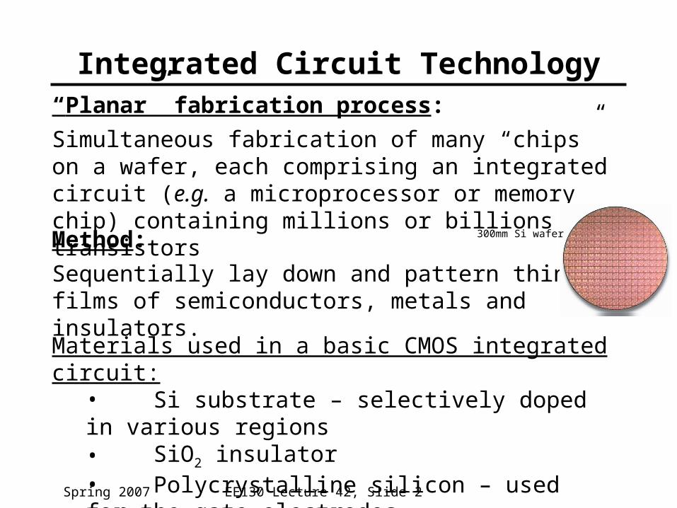
• A series of steps is used to form the deep source / drain regions as well as body contacts
• A series of steps is used to encapsulate the devices and form metal interconnections between them.
p-type Silicon Substrate
p-type Silicon Substrate

EE130 Lecture 42, Slide 14 Spring 2007
Intel’s 65 nm CMOS Technology
• Lg = 35 nm
• Tox = 1.2 nm
• Strained Si channelNMOS: tensile capping layer
PMOS: epitaxial Si1-xGex embedded in S/D
NMOSFET
PMOSFET

EE130 Lecture 42, Slide 15 Spring 2007
CMOS Inverter
n+ p+ p+ n+ n+ p+
n-well p-Si
Vin
Vout
VDD
Vin Vout
VDD
Equivalent circuit:
VSS
SiO2

EE130 Lecture 42, Slide 16 Spring 2007
Coupled parasitic npn and pnp bipolar transistors:
If either BJT enters the active mode, the SCR will enter into the forward conducting mode (large current flowing between VDD and GND) if
npnpnp > 1
=> circuit burnout!Latch-up is triggered by a transient increase in current, caused by• transient currents (ionizing radiation, impact ionization, etc.)• voltage transients
• e.g. negative voltage spikes which forward-bias the pn junction momentarily
CMOS Latchup
EE130 Lecture 42, Slide 17 Spring 2007
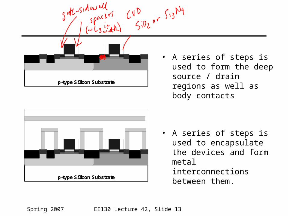
How to Prevent CMOS Latchup
(a) n-well p epitaxial layer
p+-substrate
Rsub
npn
nn+ p-sub
Rwell
pnp
“retrograde well”
(b)
1. Reduce minority-carrier lifetimes in well/substrate
2. Use highly doped substrate or wells:
EE130 Lecture 42, Slide 18 Spring 2007
IC Technology Trends
• Continued scaling of MOSFETs toward 10 nm Lg: – CMOSFETs with gate lengths below 20 nm have already been
demonstrated by leading semiconductor manufacturers.
The most advanced transistor designs are based on UC-Berkeley research (Prof’s Hu, King Liu, Bokor).
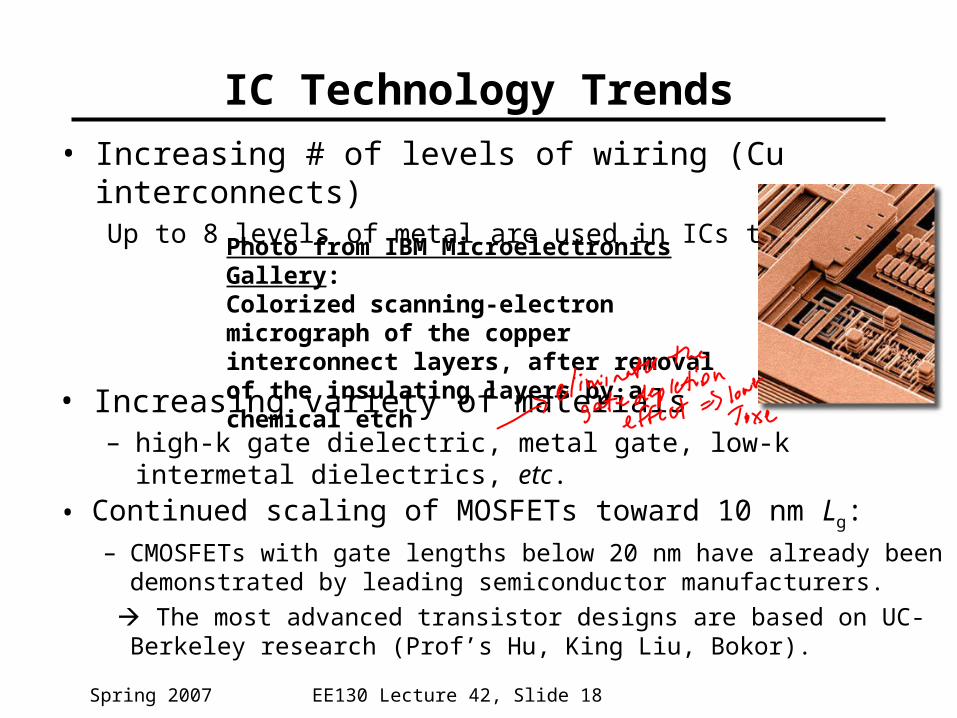
• Increasing # of levels of wiring (Cu interconnects)Up to 8 levels of metal are used in ICs today.
Photo from IBM Microelectronics Gallery:Colorized scanning-electron micrograph of the copper interconnect layers, after removal of the insulating layers by a chemical etch
• Increasing variety of materials– high-k gate dielectric, metal gate, low-k intermetal dielectrics, etc.