Embed Size (px)
Citation preview
STABILITY OF AMORPHOUS SILICON THIN FILM
TRANSISTORS AND CIRCUITS
Ting Liu
A DISSERTATION
PRESENTED TO THE FACULTY
OF PRINCETON UNIVERSITY
IN CANDIDACY FOR THE DEGREE
OF DOCTOR OF PHILOSOPHY
RECOMMENDED FOR ACCEPTANCE
BY THE DEPARTMENT OF
ELECTRICAL ENGINEERING
Advisor:
James C. Sturm
June 2013

© Copyright 2013 by Ting Liu.
All rights reserved

Abstract
i
Hydrogenated amorphous silicon thin-film transistors (a-Si:H TFTs) have been widely used for
the active-matrix addressing of flat panel displays, optical scanners and sensors. Extending the
application of the a-Si TFTs from switches to current sources, which requires continuous
operation such as for active-matrix organic light-emitting-diode (AMOLED) pixels, makes
stability a critical issue.
This thesis first presents a two-stage model for the stability characterization and reliable lifetime
prediction for highly stable a-Si TFTs under low gate-field stress. Two stages of the threshold
voltage shift are identified from the decrease of the drain saturation current under low-gate field.
The first initial stage dominates up to hours or days near room temperature. It can be
characterized with a stretched-exponential model, with the underlying physical mechanism of
charge trapping in the gate dielectric. The second stage dominates in the long term and then
saturates. It corresponds to the breaking of weak bonds in the amorphous silicon. It can be
modeled with a “unified stretched exponential fit,” in which a thermalization energy is used to
unify experimental measurements of drain current decay at different temperatures into a single
curve.
Two groups of experiments were conducted to reduce the drain current instability of a-Si TFTs
under prolonged gate bias. Deposition conditions for the silicon nitride (SiNx) gate insulator and
the a-Si channel layer were varied, and TFTs were fabricated with all reactive ion etching steps,
or with all wet etching steps, the latter in a new process. The two-stage model that unites charge
trapping in the SiNx gate dielectric and defect generation in the a-Si channel was used to interpret
the experimental results. We identified the optimal substrate temperature, gas flow ratios, and RF
deposition power densities. The stability of the a-Si channel depends also on the deposition
conditions for the underlying SiNx gate insulator. TFTs made with wet etching are more stable
than TFTs made with reactive ion etching. Combining the various improvements raised the
extrapolated 50% decay time of the drain current of back channel passivated dry-etched TFTs
under continuous operation at 20°C from 3.3 × 10⁴ sec (9.2 hours) to 4.4 × 10
7 sec (1.4 years).
The 50% lifetime can be further improved by ~2 times through wet etching process.
Two assumptions in the two-stage model were revisited. First, the distribution of the gap state
density in a-Si was obtained with the field-effect technique. The redistribution of the gap state
density after low-gate field stress supports the idea that defect creation in a-Si dominates in the
Abstract

Abstract
ii
long term. Second, the drain-bias dependence of drain current degradation was measured and
modeled. The unified stretched exponential was validated for a-Si TFTs operating in saturation.
Finally, a new 3-TFT voltage-programmed pixel circuit with an in-pixel current source is
presented. This circuit is largely insensitive to the TFT threshold voltage shift. The fabricated
pixel circuit provides organic light-emitting diode (OLED) currents ranging from 25 nA to 2.9
µA, an on/off ratio of 116 at typical quarter graphics display resolution (QVGA) display timing.
The overall conclusion of this thesis research is that the operating life of a-Si TFTs can be quite
long, and that these transistors can expect to find yet more applications in large area electronics.

Acknowledgement
iii
My PhD study at Princeton is one of the most rewarding experiences that I have had in my life
and will always be in my memory. There are many people I would like to thank who have given
me incredible help and support throughout half a decade in Princeton. I will start off by first
thanking my advisor Prof. James C. Sturm for his invaluable guidance, enlightening insight,
unwavering support and perpetual encouragement. He is an advocate to cultivate independent
researchers and encourages students to realize their dreams. His liberal style of mentoring allows
me to study at my own pace and explore the fields of my interest. It is my lifetime fortune to
have him as my advisor.
Next, I would like to thank Prof. Sigurd Wagner, for giving me the opportunity to work with him
and his research group. As one of the co-founders of large area electronics, he directs me to this
fascinating research area. When I lack confidence or feel frustrated, he is always at my back. I
really appreciate and would like to thank him for his invaluable advice and constant
encouragement. Also, I greatly appreciate the time spent by Prof. Arokia Nathan in Cambridge
and Prof. Sigurd Wagner for reading this thesis and their valuable comments. I would also like to
thank Prof. Stephen A. Lyon and Prof. Antoine Kahn for taking time to serve on my FPO
committee.
I would like to thank the present and former members of Prof. Sturm’s and Prof. Wagner’s labs,
particularly those involved in the large-area projects for their constant help and cooperation:
Bahman Hekmatshoar, Yifei Huang, Noah Jafferis, Bhadri Lalgudi, Warren Rieutort-Louis,
Josue Sanz-Robinson, Yasmin Afsar, Hongzheng Jin, Ke Long, Prashant Mandlik, Lin Han and
Wenzhe Cao, with special thanks to Warren and Noah for their help to polish the wording of this
thesis. I am also grateful to the other lab members: Sushobhan Avasthi, Jiun-yun Li, Chiao-Ti
Huang, Amy Wu, Joseph D'Silva, Ken Nagamatsu and many others, for their contribution to
make the lab full of fun and warmth.
I would also like to thank PRISM and EE staff members: Dr. Pat Watson, Dr. Mike Gaevski, Joe
Palmer, Dr. Yong Sun, Dr. Nan Yao and Jerry Poirier for their unselfish assistance with my work
in PRISM, and Sarah M. McGovern, Roelie Abdi-Stoffers, Carolyn M. Arnesen, Sheila Gunning
and Barbara Fruhling, for their generous help.
Acknowledgement
Acknowledgement
iv
My special thanks go to my friends in Princeton: Liling Wan, Meng Zhang, Yi Shao, Fei Ding,
He Wang, Yin Wang and many others, for the laughs, sweat and tears we shared. Without them,
I would not have had the courage to finish my PhD study.
Last but not least, my deepest gratitude goes to my family. My mom and dad are the most
selfless parents in the world, because they sacrificed all they own to help establish my
achievements. My husband Junfeng has partnered with me to build a happy family across half
the globe from Shanghai to New York City. My son Zale’s arrival is a surprising gift that teaches
me to appreciate the miracle of life. My son’s American grandparents, Wendy and Tommy
Williams have provided me a safe harbor to enjoy this life far away from home.
You all complete me! Thank you!
Table of Contents
v
Abstract ............................................................................................................................................ i
Acknowledgement ......................................................................................................................... iii
Chapter 1 Introduction ................................................................................................................... 1
1.1 Thin-film transistors for large-area electronics ............................................................ 1
1.2 Stability issue in TFT technologies .............................................................................. 3
1.3 Thesis outline ................................................................................................................ 5
Chapter 2 Amorphous-Silicon Thin-Film Transistors ................................................................... 8
2.1 Basic properties of a-Si ................................................................................................. 8
2.1.1 Atomic structure .................................................................................................... 8
2.1.2 Density of states .................................................................................................. 10
2.1.3 Electronic transport ............................................................................................. 13
2.1.4 Metastability ........................................................................................................ 14
2.2 Structures and operation principle of a-Si TFTs ........................................................ 17
2.2.1 Bottom-gate structure .......................................................................................... 17
2.2.2 Operation of a-Si TFTs ....................................................................................... 19
2.2.3 Characterization of a-Si TFTs ............................................................................. 21
Chapter 3 Fabrication of Amorphous-Silicon Thin-Film Transistors.......................................... 27
3.1 PECVD growth of thin films in a-Si TFTs ................................................................. 27
3.1.2 Parameters in PECVD growth............................................................................. 27
3.1.3 a-Si growth .......................................................................................................... 28
3.1.4 SiNx growth ......................................................................................................... 32
3.2 Dry-etch and wet-etch fabrication process flows ....................................................... 35
3.3 Comparison of dry-etch and wet-etch processes ........................................................ 42
Table of Contents

Table of Contents
vi
Chapter 4 Two-Stage Model for Lifetime Prediction of Highly Stable a-Si TFTs ..................... 45
4.1. Instability mechanisms in a-Si TFTs .......................................................................... 45
4.1.1 Modeling defect creation in a-Si ......................................................................... 45
4.1.2 Modeling charge trapping in the gate SiNx ........................................................ 52
4.1.3 Summary of instability models for a-Si TFTs ..................................................... 53
4.2. Sample preparation and bias-temperature-stress measurement .................................. 54
4.3. Two-stage model for lifetime prediction .................................................................... 55
4.3.1 Single stretched-exponential fit ........................................................................... 56
4.3.2 Unification of time and temperature ................................................................... 57
4.3.3 Unified stretched exponential fit (Stage II model) .............................................. 58
4.3.4 Two-stage model ................................................................................................. 60
4.4. Discussion ................................................................................................................... 62
4.5. Summary and conclusion............................................................................................ 65
Chapter 5 Optimization of Fabrication Conditions for Highly Stable a-Si TFTs ........................ 69
5.1. Introduction ................................................................................................................ 69
5.2. Effects of deposition conditions on a-Si TFT stability ............................................... 70
5.2.1 SiNx gate insulator deposition ............................................................................. 73
5.2.2 a-Si channel layer deposition .............................................................................. 74
5.2.3 Discussion ........................................................................................................... 76
5.3. The stability of wet and dry-etched TFTs .................................................................. 77
5.3.1 DC characteristics comparison ............................................................................ 77
5.3.2 Comparison of dry and wet-etched a-Si TFTs .................................................... 78
5.3.3 Discussion ........................................................................................................... 81
5.4. Summary and conclusion............................................................................................ 81

Table of Contents
vii
Chapter 6 Redistribution of Gap State Density after Low Gate-Field Stress .............................. 86
6.1. Theory of field-effect technique to determine gap state density ................................ 86
6.1.1 Assumptions and approximations ....................................................................... 86
6.1.2 Determination of gap state density ...................................................................... 88
6.1.3 Relation between gate voltage and surface potential [9]..................................... 89
6.1.4 Sheet conductance calculation ............................................................................ 89
6.2. Sample preparation and measurement ........................................................................ 90
6.3. Experiment results and gap state density determination ............................................ 90
6.4. Discussion ................................................................................................................... 93
6.5. Summary and conclusion............................................................................................ 95
Chapter 7 Drain-Bias Dependence of Drain Current Degradation .............................................. 99
7.1. Modeling of threshold voltage shift with drain-bias ................................................ 100
7.2. Numerical simulation of drain current degradation .................................................. 101
7.3. Analytical solution of drain current degradation ...................................................... 103
7.4. Experimental and modeling results .......................................................................... 104
7.5. Discussion ................................................................................................................. 107
7.6. Summary and conclusion.......................................................................................... 112
Chapter 8 3-TFT Highly Stable OLED Pixel Circuit with In-pixel Current Source ................. 114
8.1. Pixel circuit operation ............................................................................................... 114
8.2. Pixel circuit fabrication and characterization ........................................................... 117
8.3. Stability analysis and preliminary experimental results ........................................... 120
8.4. Summary and conclusion.......................................................................................... 122

Table of Contents
viii
Chapter 9 Summary and Future Work ....................................................................................... 125
9.1. Summary ................................................................................................................... 125
9.2. Future work............................................................................................................... 126
Appendix A Publications and Presentations from Thesis Research .......................................... 128
A.1. Journal and conference publications ..................................................................... 128
A.2. Conference presentations ...................................................................................... 129
Appendix B Substrate temperature Calibration ......................................................................... 131

Chapter 1: Introduction
1
Introduction
This chapter introduces the motivation behind the work presented in this thesis and the
organization of the thesis chapters. Thin-film transistors (TFTs) for large-area electronics and in
particular the stability requirement will be briefly reviewed. The stability issue is a common
challenge that all new TFT technologies are facing.
1.1 Thin-film transistors for large-area electronics
Large-area electronics is a rapid growing field expected to impact all aspects of human life such
as energy, health and the environment. Large area applications include but are not limited to:
switching and driving devices for active matrix flat panel displays (AMFPDs) based on liquid
crystal pixels (AMLCDs) and organic light emitting diodes (AMOLEDs), medical imagers,
pressure sensors, low-power communication and energy harvesting [1] (Fig. 1.1). The flat-panel
display industry is currently the largest industry in the field of large-area electronics – a market
worth in excess of $90Bn (source: DisplaySearch Inc). Thin-film transistors (TFTs) have in the
past 20 years become the “rice” of the electronic flat panel industry, just as silicon chips were
earlier the “rice” of the electronic computer revolution [2]. At present, the entrenched technology
in large area electronics applications, especially the backplanes of AMLCDs, is based on TFTs
comprising hydrogenated amorphous silicon (a-Si:H) active layers [3]. However, as the
applications for large-area electronics expand, other TFT technologies, like polycrystalline
silicon (poly-Si), microcrystalline silicon (µc-Si), organic semiconductors and metal oxides draw
growing attention from researchers. Comparion of different TFT technologies is summerized in
Table 1-I. Although different large area applications require different performance standards, the
general guidelines for the requirements of TFTs in large area electronics are: low processing
temperature (~300⁰C for glass substrates, ~350⁰C for metal foil substrates and ~150⁰C for plastic
substrates), low leakage current, high on/off ratio, low voltage operation, small area, high
uniformity and high stability [4]. Among all these requirements, stability is always important for
a new TFT technology to get commercialized.
Chapter 1

Chapter 1: Introduction
2
Sharp 108” AMLCD TV [5]
Samsung flexible AMOLED
display [6]
dpiX amorphous silicon (a-Si) X-ray image
sensor [7]
E-skin with pressure sensors [1]
Prototype for low-power communication [8]
Nellis Air Force Solar Power Plant,
Nevada, USA [9]
Fig. 1.1. Large area applications including AMLCDs, AMOLEDs, medical imagers, pressure
sensors, low-power communication and energy harvesting.

Chapter 1: Introduction
3
Table 1-I. Comparison of different TFT technologies [4, 10, 11]
Attribute a-Si µc-Si Poly-Si organic Metal oxides
Circuit type NMOS NMOS /
PMOS
NMOS /
PMOS PMOS NMOS
Mobility low higher
than a-Si high low high
Stability issue stable stable issue under
investigation
Uniformity high potentially
high improving improving high
Manufacturability mature RF
PECVD? new
has
potential has potential
Cost low low high potentially
low Low
Flexible substrate promising promising uncertain promising promising
1.2 Stability issue in TFT technologies
While the a-Si TFT has long been the workhorse in the AMLCD industry, its stability issue
becomes the bottleneck that hinders its further application in large-area electronics. Under
positive gate bias, the threshold voltage of a-Si TFTs increases with time due to charge trapping
in the gate nitride and defect creation in the a-Si channel [12]. This problem is not critial in
AMLCDs since LCDs are non-conducting and switching TFTs in LCD pixels are working in
operation with only ~0.1% duty cycle. However, the threshold voltage instability becomes
serious when the TFTs are needed for accurate current supply or measurements, such as in the
pixels of AMOLED displays and x-ray image sensors. In particular, the AMOLED pixels operate
in DC and the OLED current depends directly and continuously on the TFT threshold voltage.
Therefore as the threshold voltage increases, the OLED current supplied by the TFTs and thus
the pixel brightness drops. This leads to various issues including the distortion of color balance
in pixels, which is a serious problem [13] because human eyes are sensitive to the brightness
drop and can detect a degradation of only 5% (Fig. 1.2).

Chapter
From Ta
The eme
survive in
Fig.
This thes
− R
in
in
− H
y
(F
el
− T
te
1: Introducti
able 1-I, a-Si
rging and fa
n the field o
Drop
2% Red Drop
5% Red Drop
10% Red Drop
20% Red Drop
. 1.2. The
c
sis focuses o
Resolving th
nfrastructure
nfrastructure
Highly stable
ears from ro
Fig. 1.3) [14
lectronics;
The stability
echnologies,
ion
i is not the o
ast growing
f large area
Drop
Drop
2% Green Drop
5% Green Drop
10% Green Drop
20% Green Drop
2% Blue Drop
5% Blue Drop
10% Blue Drop
20% Blue Drop
degradation o
omponents w
n the stabilit
he stability
e to be use
e employing
e a-Si TFTs
oom tempera
4] and make
analyzing
because the
only TFT te
organic and
electronics.
of white color
with respect to
ty of a-Si TF
issue of a-
ed for the e
new materia
with extrapo
ature measu
e a-Si TFTs
and optimiz
e instability m
echnology th
d metal oxid
r as a result o
o the others; (b
FTs for the f
-Si enables
emerging ap
als [13];
olated DC sa
urements out
promising t
zing method
mechanisms
hat is confro
de TFTs also
f the drop of
b) The figure
following rea
the mainst
pplications
aturation cur
tperforms or
to stay in th
d of a-Si ca
s can be com
onted with th
o need to be
one of the blu
discoloration
asons:
tream a-Si
instead of r
rrent half-lif
rganic and m
he play grou
an be applie
mmon.
he stability i
proven stab
ue, red and gr
n [13]
TFT produ
requiring a
fe of 100 to
metal oxide T
und of large
ed to other
4
issue.
ble to
reen
uction
new
1000
TFTs
e area
TFT

Chapter 1: Introduction
5
10-2 10-1 100 101 10210-2
100
102
104
106
108
1010
P.U. Improved Process B
P.U. Improved
P.U.
[13] ZTO (ZnO/SnO2)
[12] ZnO
[11] IGZO(In2O3/Ga2O3/ZnO)
[10] ZnO[9] PQ-12
[2]a-Si:H
[1] a-Si:H
[3] a-Si:H
[8] Pentacene
[7] Pentacene
τ 10%
(sec
)
Channel Sheet Resistance (MΩ / )
1000 Cd/m2 AMOLED Operation
[4] a-Si:H
[5] a-Si:H
[6] a-Si:H 1 month
1 day
10 years
1 minute
1 second
hr1
1 yearProcess A
Standard Process
Fig. 1.3. The 10% color decay lifetime vs channel sheet resistance for a-Si, organic and metal
oxide TFT technologies (P.U. refers to “Princeton University”) [14]
1.3 Thesis outline
The topic of this thesis is stability characterization, optimization and circuit compensation for a-
Si TFTs.
Chapter 2 introduces a basic knowledge of a-Si and a-Si TFTs, with focuses on the stability
related properties of a-Si and the bottom-gate back-channel passivated (BCP) structured a-Si
TFTs and their operation principles.
Chapter 3 emphasizes on the fabrication of the a-Si TFTs. It presents the PECVD growth of
silicon nitride (SiNx) and a-Si layers. Then a new full wet-etch fabrication process that has the
same deposition steps as the dry-etch process is introduced along with the dry-etch process.
Chapter 4 develops a two-stage model for lifetime prediction of highly stable a-Si TFTs under
low-gate field stress. This model is based on the physical mechanisms in a-Si and SiNx instability
and can be used as a relible tool to quantify the stability of a-Si TFTs.
Chapter 5 applies the two-stage model to characterize the stability of a-Si TFTs fabricated with
different deposition conditions and etching methods. It provides guidance to optimize fabrication
conditions for highly stable a-Si TFTs.

Chapter 1: Introduction
6
Chapter 6 and Chapter 7 discuss two important assumptions for the two-stage model. In Chapter
6, the gap state density in a-Si before and after low gate-field stress is determined from the field-
effect technique. The redistribution of the gap state density after the gate-field stress proves that
defect creation occurs in a-Si TFTs under low gate-field stress. Chapter 7 calculates the drain
current degradation under both drain and gate bias, without assuming the channel is uniform as
in Chapter 4 when the two-stage model is developed.
Chapter 8 presents a new 3-TFT voltage-programmed pixel circuit with an in-pixel current
source. This circuit is largely insensitive to the TFT threshold voltage shift and can be used to
further promote the application of a-Si TFTs in AMOLED displays.
Chapter 9 summarizes the thesis and makes suggestions for future work in this area.

Chapter 1: Introduction
7
References:
[1] E. E. Cantatore, Applications of Organic and Printed Electronics: Springer, 2013. [2] C. R. Kagan and P. Andry. (2003). Thin-film transistors. Available:
http://marc.crcnetbase.com/isbn/9780203911778 [3] C. D. Dimitrakopoulos and P. R. L. Malenfant, "Organic thin film transistors for large
area electronics," Advanced Materials, vol. 14, pp. 99-+, Jan 16 2002. [4] A. Flewitt and A. Nathan, "Thin-Film Silicon Materials and Devices for Large-Area and
Flexible Solar Cells and Electronics," presented at the Materials Research Society Symposium A Tutorial Program, San Fancisco, CA, 2010.
[5] (2010). Electronics makers face shortage of LCD panels for TV: Sharp. Available: http://phys.org/news193317594.html
[6] K. Xu. (2010). Samsung Showing Off New Flexible AMOLED Display In Japan. Available: http://www.hardwaresphere.com/2010/11/05/samsung-showing-off-new-flexible-amoled-display-in-japan/
[7] (2013). dpiX Amorphous Silicon (a-Si) X-ray Image Sensor Array Technology. Available: http://www.dpix.com/technology/default.aspx
[8] L. Huang, W. Rieutort-Louis, Yingzhe Hu, J. Sanz-Robinson, S. Wagner, J. C. Sturm, and N. Verma, "A Super-Regenerative Radio on Plastic Based on Thin-Film Transistors and Antennas on Large Flexible Sheets for Distributed Communication," presented at the IEEE International Solid-State Circuits Conference (ISSCC), San Francisco, CA, 2013.
[9] "Nellis Solar Power Plant solar panels at Nellis Air Force Base." [10] E. Fortunato, P. Barquinha, and R. Martins, "Oxide Semiconductor Thin-Film
Transistors: A Review of Recent Advances," Advanced Materials, vol. 24, pp. 2945-2986, Jun 12 2012.
[11] A. Nathan, D. Striakhilev, R. Chaji, S. Ashtiani, C.-H. Lee, A. Sazonov, J. Robertson, and W. Milne, "Backplane Requirements for Active Matrix Organic Light Emitting Diode Displays," Materials Reseach Society Symposium Proceedings, vol. 910, pp. 373-387, 2006.
[12] M. J. Powell, S. C. Deane, I. D. French, J. R. Hughes, and W. I. Milne, "A Defect-Pool Model for near-Interface States in Amorphous-Silicon Thin-Film Transistors," Philosophical Magazine B-Physics of Condensed Matter Statistical Mechanics Electronic Optical and Magnetic Properties, vol. 63, pp. 325-336, Jan 1991.
[13] B. Hekmatshoar, "Highly stable amorphous silicon thin film transistors and integration approaches for reliable organic light emitting diode displays on clear plastic," Thesis (Ph D), Princeton University, 2010.
[14] B. Hekmatshoar, S. Wagner, and J. C. Sturm, "Tradeoff regimes of lifetime in amorphous silicon thin-film transistors and a universal lifetime comparison framework," Applied Physics Letters, vol. 95, Oct 5 2009.
Chapter 2: Amorphous-Silicon Thin
Amorphous
Amorphous silicon thin-film transistor
addressing circuits in flat panel displays, optical scanners and
their first demonstration in 1976
reviews the fundamental knowledge and concepts that will be further discussed in the thesis
starting first with an overview of the basic pr
related properties. Subsequently, the typical structures of a
the bottom-gate back-channel-passivated (BCP) structure which is used throughout our work.
Finally, the operation principles of a
presented.
2.1 Basic properties of a
The amorphous silicon (a-Si) discussed in this thesis is actually hydrogenated amorphous silicon,
denoted by the abbreviation symbol a
defect density and is thus not suitable for making semiconductor devices.
2.1.1 Atomic structure
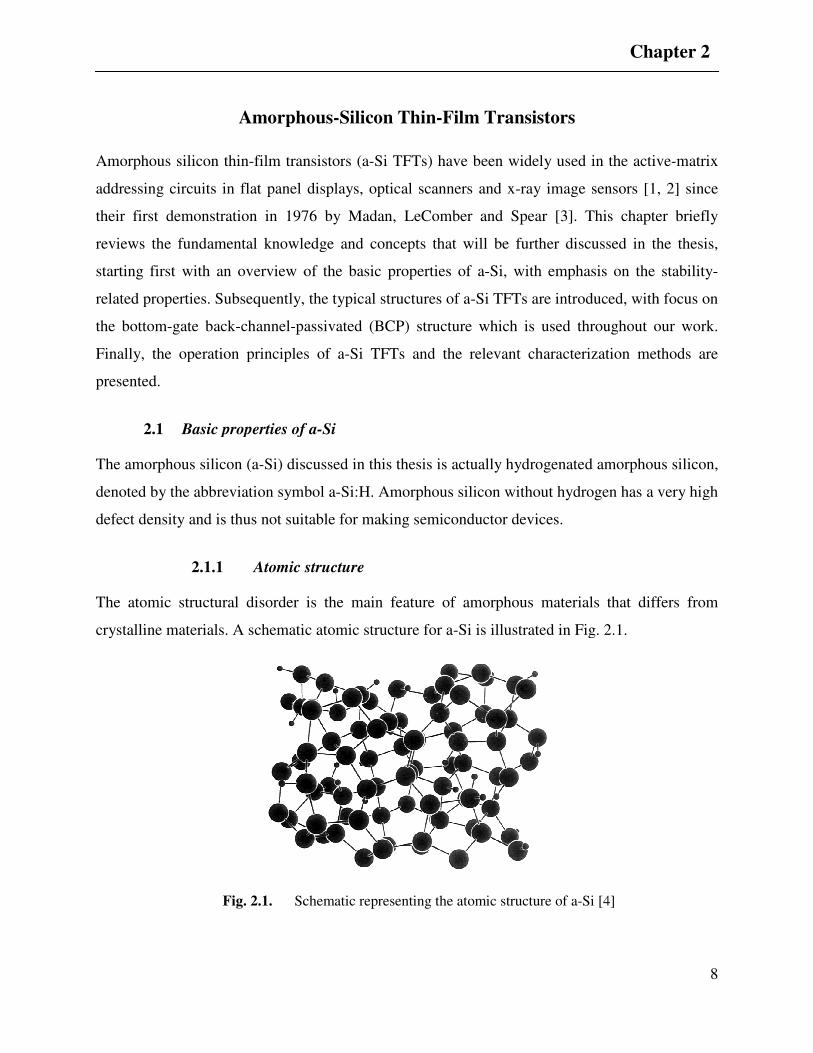
The atomic structural disorder is the main feature of amorphous materials that differs from
crystalline materials. A schematic atomic structure fo
Fig. 2.1. Schematic
Silicon Thin-Film Transistors
Amorphous-Silicon Thin-Film Transistors
lm transistors (a-Si TFTs) have been widely used in the active
in flat panel displays, optical scanners and x-ray image sensors
in 1976 by Madan, LeComber and Spear [3]. This chapter briefly
reviews the fundamental knowledge and concepts that will be further discussed in the thesis
of the basic properties of a-Si, with emphasis
related properties. Subsequently, the typical structures of a-Si TFTs are introduced, with focus on
passivated (BCP) structure which is used throughout our work.
Finally, the operation principles of a-Si TFTs and the relevant characterization methods are
Basic properties of a-Si
Si) discussed in this thesis is actually hydrogenated amorphous silicon,
symbol a-Si:H. Amorphous silicon without hydrogen has a very high
defect density and is thus not suitable for making semiconductor devices.
Atomic structure
The atomic structural disorder is the main feature of amorphous materials that differs from
crystalline materials. A schematic atomic structure for a-Si is illustrated in Fig. 2.1
Schematic representing the atomic structure of a-Si [4
8
been widely used in the active-matrix
image sensors [1, 2] since
This chapter briefly
reviews the fundamental knowledge and concepts that will be further discussed in the thesis,
on the stability-
Si TFTs are introduced, with focus on
passivated (BCP) structure which is used throughout our work.
and the relevant characterization methods are
Si) discussed in this thesis is actually hydrogenated amorphous silicon,
en has a very high
The atomic structural disorder is the main feature of amorphous materials that differs from
Fig. 2.1.
4]
Chapter 2

Chapter 2: Amorphous-Silicon Thin-Film Transistors
9
Fig 2.1 illustrates that a-Si is a disordered form of silicon consisting of a backbone of silicon
atoms (big spheres in Fig. 2.1) with hydrogen atoms (small spheres in Fig. 2.1). Experimentally,
the information of the atomic structure can be obtained by x-ray diffraction [5], electron
diffraction [6], neutron diffraction [7] and EXAFS (extended x-ray absorption fine structure) [8].
An example of a typical radial distribution function (also known as pair distribution function,
this shows the average atomic density at distance � from any atom) obtained from x-ray
diffraction is shown in Fig. 2.2..
Fig. 2.2. Example of the radial distribution function of a-Si obtained from x-ray scattering [4, 5]
The radial distribution function of a-Si suggests that a-Si is not completely disordered and has a
degree of short range order. Similar to crystalline Si, Si atoms in a-Si are generally bonded to
four neighbors at tetrahedral angles (� = 109°) with a Si-Si bond length of � = 0.23 nm.
However, unlike crystalline Si with determined bond angle and bond length, a-Si has a ~10%
spread in bond angle and a ~1% spread in bond length [4]. These strained bonds are weak bonds.
About 10% Si atoms with missing bonds and they are mostly passivated with hydrogen. The
remaining 1015
to 1016
cm-3
so-called “broken” bonds are not passivated with hydrogen and
become structural defects [9]. The short range order in the a-Si atomic structure allows the
material to retain some useful semiconductor properties of crystalline Si. However, the lack of
long range order provides a-Si with unique electronic and optical properties.

Chapter 2: Amorphous-Silicon Thin-Film Transistors
10
2.1.2 Density of states
The electronic properties of amorphous solids depend critically on the density of states
distribution. The atomic structure of a-Si discussed earlier determines the density of states
distribution, a model of which can be represented by Fig. 2.3.
Valence Band
Mobility Edge
Conduction Band
Mobility Edge
Deep
DefectsExtended
States
Extended
States
Valence
Band Tail
EnergyEcEv
Conduction
Band Tail
Mobility
Gap
EF
Fig. 2.3. Schematic a-Si density of states distribution
The short range order in a-Si results in a pseudo band gap [10], thereby enabling semiconducting
properties. This pseudo band gap can be understood as a mobility gap. Within the mobility gap,
the states are the result of disorder in the atomic structure; these are localized states. The weak
bonds which result from the spreads in bond length and bond angle are the cause for the band
tails. The structural defects from dangling bonds result in electronic states close to the mid gap.
Beyond the mobility edges, the states are termed “extended states” and are similar to the states in
crystalline Si.
The density of states can be determined with spectroscopy techniques, which generally can be
divided into three categories [10]:
− Electron-spin resonance (ESR): by detecting singly occupied states (D0), the equilibrium
spin density can only correctly measure the defect density in undoped a-Si [4];
− Optical defect spectroscopy: including photocurrent spectroscopy (PCS), photothermal
deflection spectroscopy (PDS) and photoacoustic spectroscopy (PCS);

Chapter 2: Amorphous-Silicon Thin-Film Transistors
11
− Space charge spectroscopy: including field-effect (FE) measurements, deep-level
transient spectroscopy (DLTS) and space charge limited current (SCLC) measurements.
Among all the above techniques, field-effect measurement was the first technique to obtain
density of states distribution in a-Si [3, 4] and it will be discussed in detail in Chapter 6.
As shown in Fig. 2.3, the density of states distribution contains the following major parts:
− Band tails
It has been proven by a variety of measurements [11-13] that both the valence band tail and the
conduction band tail have an exponential distribution extending 0.1 eV to 0.5 eV below the
corresponding mobility edge [4]. The slope of the band tails are often described by characteristic
temperatures �� for the valence band tail and �� for the conduction band tail.
The valence band tail states density can be expressed as [4]
��� = ���exp−/���� (2. 1)
The logarithmic slope is about 50 meV / dec, with �� ≈ 500 K [12, 13].
The conduction band tail states density can be expressed with
��� = ���exp−/���� (2. 2)
The logarithmic slope is about 30 meV / dec, with �� ≈ 300 K [12-14].
The Urbach energy [15] obtained from optical absorption measurements gives a good measure of
valence band slope, because the valence band tail is broader than the conduction band tail [13].
The density of states density at the mobility edges (��� and ���) is about 3 ×10²¹
cm-3
eV-1
[4].
− Deep defects
A dangling bond defect can exist in three charge states D+, D
0 and D
- depending on the position
of the Fermi level [4]. The defect is neutral (D0) when singly occupied, can have an electron
excited out of (or equivalently have a hole trapped into) the neutral bond, leaving a positively
charged center D+. Alternatively, the dangling bond defect can be occupied by a second electron
and become a negatively charged state D- [3]. According to the widely accepted concept of the

Chapter 2: Amorphous-Silicon Thin-Film Transistors
12
“defect-pool model” [11, 16-20], the dangling bonds form at the sites which minimize their
formation energy, so the characteristic energy and density of deep defects depend on the Fermi
energy during equilibration [16]. Thus, the distribution of deep defects can be greatly varied for
a-Si prepared under different conditions (as shown in Fig. 2.4). The most common models
describe the deep defect density as either following a Gaussian distribution [18, 21, 22] or an
exponential distribution [14]. The exponential distribution of deep defect density is similar to the
band tail distribution but with a large characteristic temperature, and it can be viewed as the tail
part of the Gaussian distribution. In reality, the deep defect density distribution can be considered
as a superposition of the Gaussian distributions for D+, D
0 and D
- [23].
Fig. 2.4. Density of states distribution of n-type a-Si with different phosphorus doping levels
measured by DLTS [24]; the distribution of deep defects varies with doping level.
− Extended states
Electrons in the extended states have higher mobility than in the localized states, and the
mobility is known as free carrier mobility or band mobility ��. The distribution of extended
states in a-Si can deviate from the parabolic distribution as in crystalline Si, and a linear density
of states near and above the valence band edge has been reported [20].
− Mobility gap

Chapter 2: Amorphous-Silicon Thin-Film Transistors
13
The mobility gap separates extended and localized states, and can be reliably measured with the
internal photoemission measurement [25]. Mobility gap was roughly estimated with the optical
gap, which is derived by Tauc model from an extrapolation of parabolic band edge with the
optical absorption coefficient [22]. However, optical determinations of the band gap for a-Si tend
to underestimate the mobility gap [26].
2.1.3 Electronic transport
There are three main conduction mechanisms in a-Si [4] as illustrated in Fig. 2.5.
Density of States
EC
EF
Extended state
conduction
Band tail
conduction
Hopping
at EF
Fig. 2.5. Illustration of the three main conduction mechanisms in a-Si [4]
− Extended state conduction: the conduction through thermally activated carriers from the
Fermi energy to above the mobility edge;
− Band tail conduction: a thermally activated tunneling process [10] of hopping from site to
site. At very low temperatures approaching 0K, this type of conduction does not take
place;
− Hopping conduction at the Fermi energy: this occurs when the density of states is large
enough at the Fermi energy for significant tunneling of electrons. The conduction can be
neglected in a-Si:H with low deep defect density.
The carrier mobility is an alternative measure of the conductivity and they can related with the
following relation [4]
� = ��� = ����, ������ (2. 3)
Chapter 2: Amorphous-Silicon Thin-Film Transistors
14
Where � is the carrier density,�� is the density of states, �, �� is the Fermi function, �� is the mobility at a specific energy level.
In n-type a-Si and a-Si TFTs under positive gate voltage, the Fermi energy � is in the
conduction band tail. In p-type a-Si, � is in the valence band tail. Thus, the mobility of carriers
in band tails is of great interest. The mobility will be limited by frequent trapping in the tail
states and is known as the effective carrier mobility or drift mobility � . The simplest model for
explanation is the multiple trapping model, in which carriers move at the mobility edges and
interact with tail states by trapping and thermal release [10]. The drift mobility can be related to
the band mobility with the following relation [4]
� = ��/1 + �#$%&� (2. 4)
Where �#$%& is the ratio of the time that the carrier spends in localized traps to that spent in
mobile states. The band mobility is 1 – 10 cm2 / V·s for both electrons and holes [27, 28]. The
reported drift mobility is ≤ 4 cm2 / V·s for electrons [29] and ≤ 0.01 cm
2 / V·s for holes [30].
2.1.4 Metastability
In a-Si, the disorder in structure results in the afore-mentioned weak bonds and dangling bonds.
These two states are alternatives to each other, leading to the metastable configurational
coordinate diagram as shown in Fig. 2.6 with two energy wells. The energy barrier ' arises
from the bonding energy of weak bonds, which is higher for stronger bonds and smaller for
weaker bonds. The energy difference is the defect formation energy () and determines the
dangling bond density in thermal-equilibrium [4].

Chapter 2: Amorphous-Silicon Thin-Film Transistors
15
Fig. 2.6. Configurational coordinate diagram of a weak bond state and a dangling bond state
separated by a potential energy barrier '
The conversion of weak bonds into dangling bonds is known as defect creation and the reverse
process is defect annealing. The defect creation process can be illustrated with the density of
states redistribution in Fig. 2.7.
Density o
f S
tate
s
(in log s
cale
)
Fig. 2.7. Schematic density of states redistribution as a result of defect creation
As shown in Fig. 2.7, the created dangling bonds from weak bonds result in additional defect
states. Defect creation is an important mechanism responsible for the instability issues in a-Si.
The most widely-study defect creation phenomena include light-induced degradation in a-Si,
particularly for a-Si solar cells [31-33] and the threshold voltage instability of a-Si TFTs [34,
35]. The latter will be further discussed in Chapter 4.

Chapter 2: Amorphous-Silicon Thin-Film Transistors
16
Two classes of models are widely used to explain the metastability in a-Si: thermal-equilibrium
models and bond-breaking models [10].
− Thermal-equilibrium models
In thermal-equilibrium, the concentration *+� of a certain structural configuration + is
determined by the Gibbs free energy ,+� = -+� − �.+� of this configuration through the
relation
*+� ∝ exp 0− �1�23 4 = exp
51�3 �exp−
61�23 � (2. 5)
The enthalpy -+� = (+� − 78, (+� is the formation energy and .+� is the entropy. In a
solid, the changes in the pressure 7 and the volume 8 are negligible. Thus, the enthalpy -+� can be equated with the formation energy (+� without significant error [4].
Equation (2. 5) can be used to explain the field-effect bias induced defect creation in a-Si TFTs,
because the formation energy is dependent on the Fermi level by
(+� = (�+� − |� − +�| (2. 6)
Where (�+� is the formation energy of defect configuration without field-effect bias, � is the
Fermi energy position, and +� is the electronic level of the created defect under field-effect
bias. The term |� − +�| describes the gain in total energy for a defect that can exchange
charge with the Fermi level [10].
Combining (2. 5) and (2. 6), it can be obtained that
*+� ∝ exp 0|:;<:1�|23 4 (2. 7)
This means that the concentration of defects is dependent on the Fermi-level. Under field-effect
bias, the increase in Fermi-level leads to the increase in the defects. The main disadvantage of
the thermal-equilibrium models is that although it can explain the macroscopic changes in
metastable states, it gives little microscopic information.
− Bond-breaking models

Chapter 2: Amorphous-Silicon Thin-Film Transistors
17
The bond-breaking models depict the microscopic defect creation process from the rupture of
weak bonds. The thermal-equilibrium between the weak bonds and the dangling bonds is broken,
such as in a-Si solar cells under light illumination or in a-Si TFTs under gate-field bias. In a-Si
solar cells, the energy released by the nonradioactive recombination of photo excited electron-
hole pairs lowers the energy barrier ' in Fig. 2.6, so the defect creation rate is much higher than
the defect annealing rate. In a-Si TFTs, electron in the channel induce weak bonds to break into
dangling bonds, this process is immediately reversible unless the dangling bonds relax into stable
configuration. The stabilization step actually created the barrier energy for the defect annealing
process. Generally, there are two microscopic models for the stabilization step - hydrogen-
diffusion-controlled defect-relaxation (HCR) model [33, 36, 37] and defect-controlled defect-
relaxation (DCR) model [38]. These two models will be elaborated in Chapter 4.
2.2 Structures and operation principle of a-Si TFTs
As a special kind of field-effect transistor, a thin-film transistor (TFT) is composed of a stack of
thin films including a semiconducting active layer, a gate dielectric layer and metallic contacts
over a supporting substrate [39]. In a-Si TFTs, the active layer is intrinsic a-Si and the gate
dielectric typically is silicon nitride (SiNx). Because the hole mobility of a-Si is very low, only n-
type a-Si TFTs are available in practical applications. For n-type a-Si TFTs, between the intrinsic
a-Si layer and the source / drain metal, a layer of phosphorous doped n+ a-Si is usually used to
ensure low resistance ohmic source/drain contacts.
2.2.1 Bottom-gate structure
The most commonly used a-Si TFT structure is the inverted-staggered structure. This is because
this structure has easy fabrication processes and gives good electrical performance. The term
“inverted” means that the position of the gate is on the bottom. The term “staggered” in contrast
to “coplanar” refers to the fact that the source / drain electrodes and the gate electrode are located
on different sides of the active layer. The inverted structures are also called bottom-gate
structures. The TFTs with the inverted-staggered structure can be subdivided into two types – bi-
layer (back-channel etched / cut) and tri-layer (back-channel passivated) [40] (Fig. 2.8).

Chapter 2: Amorphous-Silicon Thin-Film Transistors
18
(a) Back-channel etched (BCE) structure
(b) Back-channel passivated (BCP) structure
Fig. 2.8. Schematic cross-section of (a) back-channel etched (BCE) and back-channel passivated
(BCP) standard a-Si TFT structures.
The inverted (bottom-gate) a-Si TFT structures have the active a-Si layer on top of the gate SiNx
dielectric layer. It has been reported that the interface with a-Si on top of SiNx as in the bottom-
gate structure is better than interfaces with SiNx on top of a-Si as in a top-gate structure, with a
lower interface charge density and lower hydrogen concentration [41-43]. As a result, bottom-
gate a-Si TFTs have a higher field-effect mobility, lower threshold voltages and lower
subthreshold slopes than top-gate a-Si TFTs.
In the bi-layer (BCE) structure, the gate SiNx, intrinsic and doped n+ a-Si are consecutively
deposited without breaking vacuum. Since the etchant of n+ a-Si also etches the active a-Si layer,
a slight over-etch of the back channel cannot be avoided. Compared with the bi-layer (BCE)
structure, the tri-layer (BCP) structure has one extra layer of SiNx on top of the active a-Si layer.
The gate SiNx, intrinsic a-Si and passivation SiNx are consecutively deposited in one-pump
down. The passivation SiNx layer serves as an etch-stop during the n+ a-Si etching, and thus the
BCP structure is also called an etch-stop structure.
The advantages of the BCP structure come from the protection granted by the passivation SiNx
layer. TFTs with BCP structure can have very thin active layers (as thin as ~50 nm), because the

Chapter 2: Amorphous-Silicon Thin-Film Transistors
19
passivation SiNx layer prevents the under-cut of the a-Si back channel. This shortens the a-Si
deposition time, decreases the leakage current through the a-Si layer and reduces the S/D -
channel parasitic resistance [44]. By preventing the back channel from the exposure to the
reagents during the n+ a-Si film etching (the strong alkaline solution in wet-etching process or
plasma damage in dry-etching process) and the ambient during operation, back-channel
passivated TFTs can have higher field-effect mobility [44] and better threshold voltage stability
[45]. However, the BCP structure needs an extra deposition step and an extra photolithography
step, so it is more complicated in fabrication than the BCE structure. Another drawback of the
BCP structure is that the length of the passivation SiNx determines the channel length, so the
channel length is more difficult to scale down than the BCE structure. For this thesis, the BCP
structure is used because the threshold stability is the key concern.
2.2.2 Operation of a-Si TFTs
Because of the negligible hole mobility and the hole blocking at the source / drain contact by n+
a-Si, the contribution of holes will be ignored in the following analysis. The operation of a-Si
TFTs can be interpreted with the band diagram of an a-Si TFT as shown in Fig. 2.9.
(a) Band diagram (b) Density of states distribution
Fig. 2.9. Band diagram of an a-Si TFT under positive gate bias and density of states distribution.
Under positive gate bias, the band bends with the Fermi level near the SiNx / a-Si interface deep
into band tails. The band bending profile can be calculated by solving the Poisson’s equation

Chapter 2: Amorphous-Silicon Thin-Film Transistors
20
)=>?�)?= = − @?�
ABC (2. 8)
Where D is the distance away from the SiNx / a-Si interface in the a-Si layer. At the interface,
ED = 0� = EF = 8G − |1H|�CHB
(2. 9)
*IJF is the capacitance of the gate SiNx per unit area, and +J is the charge per unit area induced
in the channel by the gate voltage 8G with
+J = � KD��D?L� (2. 10)
The charge density distribution KD� in a-Si layer can be related to the band bending ED� with
KE� = −� � M�� − �E��N:;O (2. 11)
Where �� = PPQRSTUVU;OWX �
is the Fermi-Dirac distribution function.
From Fig. 2.3, the density of states distribution M� is composed of deep defect states M)�, band tail states M'� and extended states MY�. They result in three corresponding components
in KE� denoted as K)E�, K'E� and KYE� respectively. The schematic charge distribution is
illustrated in Fig. 2.10. Deep defect states and band tail states are localized states and the channel
conduction can be viewed mainly from electrons in the extended states, i.e. KYE� and it keeps
increasing with the increasing band bending E.
Fig. 2.10. Charge distribution as a function of band bending.

Chapter 2: Amorphous-Silicon Thin-Film Transistors
21
Fig. 2.10 shows that only a small portion of induced charge is from free electrons in extended
states. Thus, the effective field-effect mobility ��:3 can be related to the band mobility �� with
��:3 = �� 1Z1H = ��� @Z?�)?[LL� @?�)?[LL
(2. 12)
Typically, the effective field-effect mobility ��:3 a-Si TFTs is 1.2 – 1.4 cm2/V·s in laboratory
[46] and 0.3 – 0.6 cm2/V·s in production [47]. A record high ��:3 ≈ 2 cm
2/V·s has been
achieved using a SiO2–silicone hybrid dielectric [48].
The theoretical analysis of I-V characteristics can be found in Chapter 6.
2.2.3 Characterization of a-Si TFTs
Experimentally, the typical I-V characteristics of a good-performance a-Si TFT with 150 µm
channel width and 15 µm channel length are shown in Fig. 2.11.
(a) Output characteristics with 8G = 2 V – 20 V in steps of 2 V
0 5 10 15 200
0.5
1
1.5
2
2.5
3
3.5x 10
-5
Dra
in C
urr
en
t I D
(A
)
Drain Voltage VD
(V)
Saturation region Linear region

Chapter 2: Amorphous-Silicon Thin-Film Transistors
22
(b) Transfer characteristics with 8 = 0.1 V and 10 V
Fig. 2.11. I-V characteristics of a typical a-Si TFT with \ ]⁄ = 150 / 15 µm.
The off-current _̀ aa is at the sub-pA level, and the on / off current ratio is about 107. The
subthreshold slope (red line in Fig. 2.11(b)) is about 300 mV / dec.
The I-V characteristics of a-Si TFTs are similar to those obtained from conventional MOSFETs.
Thus the gradual channel model for conventional MOSFET can be used to characterize the a-Si
TFTs operating in linear regime and saturation regime [10].
In the linear region with Vc < Ve − Vf, the drain current is given by
_ = ��:3,gIJ*IJF hi j08G − 83,gIJ −Pk8 48 l (2. 13)
In the saturation region with Vc ≥ Ve − Vf, the drain current is given by
_ = ��:3,F%#*IJF hki jn8G − 83,F%#okl (2. 14)
Where ��:3,gIJ and ��:3,F%# are the effective field-effect mobility in linear and saturation
regime;83,gIJ and 83,F%# are the threshold voltage in linear and saturation regime. They can be
extrapolated from the least-square fits to transfer characteristics as in Fig. 2.12.
-10 -5 0 5 10 15 2010
-14
10-12
10-10
10-8
10-6
10-4
Gate Voltage VG
(V)
Dra
in C
urr
en
t I D
(A
)
VD = 10 V
VD = 0.1 V
Subthreshold
slope

Chapter 2: Amorphous-Silicon Thin-Film Transistors
23
(a) Linear region (b) Saturation region
Fig. 2.12. Least-square fits to transfer characteristics of the a-Si TFT.
In the linear region, ��:3,gIJ = 0.83 cm2/V·s and 83,gIJ = 1.0 V.
In the saturation region, ��:3,F%# = 1.1 cm2/V·s and 83,F%# = 0.69 V.
-10 -5 0 5 10 15 20-0.5
0
0.5
1
1.5
2
2.5
3x 10
-7
Gate Voltage VG
(V)
Dra
in C
urr
en
t I D
(A
)
-10 -5 0 5 10 15 20-1
0
1
2
3
4
5
6x 10
-3
Gate Voltage VG
(V)
Sq
ua
re R
oo
t o
f D
rain
Cu
rre
nt I D1
/2 (
A1/2
)

Chapter 2: Amorphous-Silicon Thin-Film Transistors
24
References:
[1] J. Kanicki, Amorphous and microcrystalline semiconductor devices : optoelectronic
devices. Boston: Artech House, 1991.
[2] M. J. Powell, "The Physics of Amorphous-Silicon Thin-Film Transistors," Ieee
Transactions on Electron Devices, vol. 36, pp. 2753-2763, Dec 1989.
[3] A. Madan, P. G. Lecomber, and W. E. Spear, "Investigation of Density of Localized
States in a-Si Using Field-Effect Technique," Journal of Non-Crystalline Solids, vol. 20,
pp. 239-257, 1976.
[4] R. A. Street, Hydrogenated amorphous silicon. Cambridge ; New York: Cambridge
University Press, 1991.
[5] W. Schulke, "Structural Investigation of Hydrogenated Amorphous-Silicon by X-Ray-
Diffraction," Philosophical Magazine B-Physics of Condensed Matter Statistical
Mechanics Electronic Optical and Magnetic Properties, vol. 43, pp. 451-468, 1981.
[6] A. Barna, P. B. Barna, G. Radnoczi, L. Toth, and P. Thomas, "Comparative-Study of
Structure of Evaporated and Glow-Discharge Silicon," Physica Status Solidi a-Applied
Research, vol. 41, pp. 81-84, 1977.
[7] T. A. Postol, C. M. Falco, R. T. Kampwirth, I. K. Schuller, and W. B. Yelon, "Structure
of Amorphous-Silicon and Silicon Hydrides," Physical Review Letters, vol. 45, pp. 648-
652, 1980.
[8] R. Bellissent, A. Chenevaspaule, P. Lagarde, D. Bazin, and D. Raoux, "Short-Range
Order Investigation in a-Si-H by Exafs," Journal of Non-Crystalline Solids, vol. 59-6, pp.
237-240, 1983.
[9] A. Flewitt and A. Nathan, "Thin-Film Silicon Materials and Devices for Large-Area and
Flexible Solar Cells and Electronics," presented at the Materials Research Society
Symposium A Tutorial Program, San Fancisco, CA, 2010.
[10] J. Kanicki, Amorphous and microcrystalline semiconductor devices. Volume II, Materials
and device physics. Boston: Artech House, 1992.
[11] K. Winer, I. Hirabayashi, and L. Ley, "Exponential Conduction-Band Tail in P-Doped a-
Si-H," Physical Review Letters, vol. 60, pp. 2697-2700, Jun 20 1988.
[12] T. Tiedje, J. M. Cebulka, D. L. Morel, and B. Abeles, "Evidence for Exponential Band
Tails in Amorphous-Silicon Hydride," Physical Review Letters, vol. 46, pp. 1425-1428,
1981.
[13] K. Winer and L. Ley, "Surface-States and the Intrinsic Valence Band Tail in a-Si-H,"
Journal of Non-Crystalline Solids, vol. 97-8, pp. 703-706, Dec 1987.
[14] M. Shur and M. Hack, "Physics of Amorphous-Silicon Based Alloy Field-Effect
Transistors," Journal of Applied Physics, vol. 55, pp. 3831-3842, 1984.
[15] F. Urbach, "The Long-Wavelength Edge of Photographic Sensitivity and of the
Electronic Absorption of Solids," Physical Review, vol. 92, pp. 1324-1324, 1953.
[16] M. J. Powell, S. C. Deane, I. D. French, J. R. Hughes, and W. I. Milne, "A Defect-Pool
Model for near-Interface States in Amorphous-Silicon Thin-Film Transistors,"
Philosophical Magazine B-Physics of Condensed Matter Statistical Mechanics Electronic
Optical and Magnetic Properties, vol. 63, pp. 325-336, Jan 1991.
[17] M. J. Powell, C. Vanberkel, A. R. Franklin, S. C. Deane, and W. I. Milne, "Defect Pool in
Amorphous-Silicon Thin-Film Transistors," Physical Review B, vol. 45, pp. 4160-4170,
Feb 15 1992.

Chapter 2: Amorphous-Silicon Thin-Film Transistors
25
[18] K. Winer, "Chemical-Equilibrium Description of the Gap-State Distribution in Alpha-Si-
H," Physical Review Letters, vol. 63, pp. 1487-1490, Oct 2 1989.
[19] K. Winer, I. Hirabayashi, and L. Ley, "Distribution of Occupied near-Surface Band-Gap
States in a-Si-H," Physical Review B, vol. 38, pp. 7680-7693, Oct 15 1988.
[20] H. Fritzsche, Amorphous silicon and related materials. Singapore ; Teaneck, N.J.: World
Scientific, 1989.
[21] K. Winer, "Defect Formation in Alpha-Si-H," Physical Review B, vol. 41, pp. 12150-
12161, Jun 15 1990.
[22] K. Winer, "Defects in Hydrogenated Amorphous-Silicon," Annual Review of Materials
Science, vol. 21, pp. 1-21, 1991.
[23] M. J. Powell and S. C. Deane, "Improved Defect-Pool Model for Charged Defects in
Amorphous-Silicon," Physical Review B, vol. 48, pp. 10815-10827, Oct 15 1993.
[24] D. V. Lang, J. D. Cohen, and J. P. Harbison, "Measurement of the Density of Gap States
in Hydrogenated Amorphous-Silicon by Space-Charge Spectroscopy," Physical Review
B, vol. 25, pp. 5285-5320, 1982.
[25] C. R. Wronski, S. Lee, M. Hicks, and S. Kumar, "Internal Photoemission of Holes and
the Mobility Gap of Hydrogenated Amorphous-Silicon," Physical Review Letters, vol.
63, pp. 1420-1423, Sep 25 1989.
[26] W. B. Jackson, S. M. Kelso, C. C. Tsai, J. W. Allen, and S. J. Oh, "Energy-Dependence
of the Optical Matrix Element in Hydrogenated Amorphous and Crystalline Silicon,"
Physical Review B, vol. 31, pp. 5187-5198, 1985.
[27] N. F. Mott and E. A. Davis, Electronic processes in non-crystalline materials, 2d ed.
Oxford, New York: Clarendon Press ; Oxford University Press, 1979.
[28] H. Overhof and P. Thomas, Electronic transport in hydrogenated amorphous
semiconductors. Berlin ; New York: Springer-Verlag, 1989.
[29] E. A. Schiff, "Drift-mobility measurements and mobility edges in disordered silicons,"
Journal of Physics-Condensed Matter, vol. 16, pp. S5265-S5275, Nov 10 2004.
[30] S. Dinca, G. Ganguly, Z. Lu, E. A. Schiff, V. Vlahos, C. R. Wronski, and Q. Yuan, "Hole
Drift-Mobility Measurements in Contemporary Amorphous Silicon," Materials Reseach
Society Symposium Proceedings, vol. 762, pp. A7.1.1-A7.1.6, 2003.
[31] D. L. Staebler and C. R. Wronski, "Reversible Conductivity Changes in Discharge-
Produced Amorphous Si," Applied Physics Letters, vol. 31, pp. 292-294, 1977.
[32] D. Han and H. Fritzsche, "Study of Light-Induced Creation of Defects in a-Si-H by
Means of Single and Dual-Beam Photoconductivity," Journal of Non-Crystalline Solids,
vol. 59-6, pp. 397-400, 1983.
[33] M. Stutzmann, W. B. Jackson, and C. C. Tsai, "Light-Induced Metastable Defects in
Hydrogenated Amorphous-Silicon - a Systematic Study," Physical Review B, vol. 32, pp.
23-47, 1985.
[34] C. Vanberkel and M. J. Powell, "Resolution of Amorphous-Silicon Thin-Film Transistor
Instability Mechanisms Using Ambipolar Transistors," Applied Physics Letters, vol. 51,
pp. 1094-1096, Oct 5 1987.
[35] W. B. Jackson, J. M. Marshall, and M. D. Moyer, "Role of Hydrogen in the Formation of
Metastable Defects in Hydrogenated Amorphous-Silicon," Physical Review B, vol. 39,
pp. 1164-1179, Jan 15 1989.

Chapter 2: Amorphous-Silicon Thin-Film Transistors
26
[36] J. Kakalios, R. A. Street, and W. B. Jackson, "Stretched-Exponential Relaxation Arising
from Dispersive Diffusion of Hydrogen in Amorphous-Silicon," Physical Review Letters,
vol. 59, pp. 1037-1040, Aug 31 1987.
[37] R. A. Street, C. C. Tsai, J. Kakalios, and W. B. Jackson, "Hydrogen Diffusion in
Amorphous-Silicon," Philosophical Magazine B-Physics of Condensed Matter Statistical
Mechanics Electronic Optical and Magnetic Properties, vol. 56, pp. 305-320, Sep 1987.
[38] R. S. Crandall, "Defect Relaxation in Amorphous-Silicon - Stretched Exponentials, the
Meyer-Neldel Rule, and the Staebler-Wronski Effect," Physical Review B, vol. 43, pp.
4057-4070, Feb 15 1991.
[39] Thin-film transistor. Available: http://en.wikipedia.org/wiki/Thin-film_transistor
[40] Y. Kuo, Amorphous silicon thin film transistors: Boston [u.a.] : Kluwer Academic
Publishers, 2004.
[41] A. Rolland, J. Richard, J. P. Kleider, and D. Mencaraglia, "Electrical-Properties of
Amorphous-Silicon Transistors and Mis-Devices - Comparative-Study of Top Nitride
and Bottom Nitride Configurations," Journal of the Electrochemical Society, vol. 140,
pp. 3679-3683, Dec 1993.
[42] R. A. Street and M. J. Thompson, "Electronic States at the Hydrogenated Amorphous-
Silicon Silicon- Nitride Interface," Applied Physics Letters, vol. 45, pp. 769-771, 1984.
[43] Y. Kuo, "Reactive Ion Etch Damages in Inverted, Trilayer Thin-Film Transistor,"
Applied Physics Letters, vol. 61, pp. 2790-2792, Dec 7 1992.
[44] M. Ando, M. Wakagi, and T. Minemura, "Effects of back-channel etching on the
performance of a-Si : H thin-film transistors," Japanese Journal of Applied Physics Part
1-Regular Papers Short Notes & Review Papers, vol. 37, pp. 3904-3909, Jul 1998.
[45] B. Hekmatshoar, K. H. Cherenack, A. Z. Kattamis, K. Long, S. Wagner, and J. C. Sturm,
"Highly stable amorphous-silicon thin-film transistors on clear plastic," Applied Physics
Letters, vol. 93, Jul 21 2008.
[46] C. R. Kagan and P. Andry. (2003). Thin-film transistors. Available:
http://marc.crcnetbase.com/isbn/9780203911778
[47] R. A. Street, Technology and applications of amorphous silicon. New York: Springer,
2000.
[48] L. Han, P. Mandlik, K. H. Cherenack, and S. Wagner, "Amorphous silicon thin-film
transistors with field-effect mobilities of 2 cm(2)/V s for electrons and 0.1 cm(2)/V s for
holes," Applied Physics Letters, vol. 94, Apr 20 2009.

Chapter 3: Fabrication of Amorphous-Silicon Thin-Film Transistors
27
Fabrication of Amorphous-Silicon Thin-Film Transistors
Amorphous-silicon thin-film transistors (a-Si TFTs) in this thesis were fabricated with bottom-
gate non-self-aligned processes in the back-channel passivated (BCP) structure. The silicon
nitride (SiNx) and amorphous silicon (a-Si) layers were deposited in a plasma-enhanced chemical
vapor deposition (PECVD) system at 13.56 MHz. This chapter first presents the PECVD growth
of thin films of SiNx and a-Si. Then a new full wet-etch fabrication process that has the same
deposition steps as the dry-etch process is introduced along with the dry-etch process. The
stability of dry-etched and wet-etched a-Si TFTs will be compared in Chapter 5.
3.1 PECVD growth of thin films in a-Si TFTs
Plasma enhanced chemical vapor deposition (PECVD) is widely used to grow thin film materials
for a-Si TFTs. The most common PECVD reactors are in a diode configuration with the plasma
confined between two parallel electrodes. The PECVD reactor in Princeton is in a triode
configuration, using a metal grid in the reactor to separate the plasma from the growing surface,
thereby reducing ion bombardment [1]. The triode configuration PECVD reactor with radio
frequency (RF) radiation at 13.56 MHz is used to deposit a-Si TFTs for this thesis. The substrate
temperature calibration of the PECVD system is displayed in Appendix B.
3.1.2 Parameters in PECVD growth
There are several parameters that control the PECVD growth of thin films.
− Gas pressure
The gas pressure during deposition is maintained by a throttle valve which controls the amount
of gases that are pumped out. The gas pressure determines the mean free path for collisions of
the gas molecules and influences whether the reactions happen at the growing surface or in the
gas [1]. Deposition of hydrogenated amorphous materials usually takes place at a gas pressure of
0.01 – 1 Torr with a film of material coating most of the exposed surfaces in the neighborhood of
the plasma [2].
− Gas flow rate
Chapter 3

Chapter 3: Fabrication of Amorphous-Silicon Thin-Film Transistors
28
Mass flow controllers (MFC) regulate the gas flow rates of the precursor gases before they enter
the PECVD chamber. For a given pressure, the gas flow rate controls the length of time that a
given gas molecule resides inside the chamber, known as the residence time [3]. The convenient
unit for gas flow rate is sccm (standard cubic centimeters per minute at � =273 K, 1 atm), i.e.
4.5 × 10¹⁷
molecules/second.
− RF power
The RF power determines the energy in the plasma [3] which helps the dissociation of the gas
species and therefore controls the film growth rate [1]. However, increasing the power also
increases the plasma potential and hence the ion bombardment energy [3].
− Substrate temperature
The temperature of the substrate temperature controls the chemical reactions on the growing
surface. Diffusion is a thermally activated process responsible for the transport of gas species
both on the deposition surface and in the film bulk. Thus, increasing substrate temperature
increases diffusivity [3, 4].
3.1.3 a-Si growth
The usual deposition method of intrinsic a-Si is by PECVD using silane gas (SiH4). a-Si films
can be grown between 450⁰C and 550⁰C in the absence of plasma. The plasma provides energy
to the dissociation of silane and enables the deposition of a-Si films at lower temperatures [1].
The main growth species are neutral radicals. Some silane dissociation reactions related to a-Si
growth with low energy requirement are [1]
SiH4 → SiH2 + H2 2.2 eV (3. 1)
SiH4 → SiH3 + H 4.0 eV (3. 2)
SiH4 → Si + H2 4.2 eV (3. 3)
The dominant radical responsible for the a-Si deposition is SiH3, which has a reactive dangling
bond and can be transported to the H-saturated growing surface [3] as in Fig. 3.1.

Chapter 3: Fabrication of Amorphous
Fig. 3.1.
SiH3 can add to an existing surface
neighbouring Si-H sites without
surface Si-H bond to leave a surface dangling bond
The PECVD parameters are critical for high quality a
silane:
− Substrate temperature and RF
Increasing the substrate temperature
means that more hydrogen on the surface can be abstracted. Therefore, hydrogen content of the
material reduces with the increasing substrate temperature
from the surface results dangling bonds and will be attached by
equilibrium of weak bonds and
temperature. As explained in the
weak bond density and a higher Urbach energy represents a more disordered a
3.2 shows that the Urbach energy strongly depends on the substrate temperature and
minimum around 250⁰C [4]. The defect density is lowest when the substrate
300⁰C, and this temperature is also known to
is proportional to the RF power
density all increases with the rising RF
Fabrication of Amorphous-Silicon Thin-Film Transistors
Fig. 3.1. Surface reactions on a-Si [4].
can add to an existing surface dangling bond leading to film growth, it can diffuse to the
reaction or desorbing and it can also abstract a hydrogen from a
a surface dangling bond [4-6].
are critical for high quality a-Si growth as well the hydrogen dilution in
Substrate temperature and RF power
he substrate temperature increases the diffusivity of species such as
means that more hydrogen on the surface can be abstracted. Therefore, hydrogen content of the
ncreasing substrate temperature (Fig. 3.2). The removal of hydrogen
from the surface results dangling bonds and will be attached by SiH3 radicals. As a result, the
equilibrium of weak bonds and dangling bonds distribution also depends on the substrate
the last chapter, the Urbach energy reflects the distribution
weak bond density and a higher Urbach energy represents a more disordered a-
shows that the Urbach energy strongly depends on the substrate temperature and
The defect density is lowest when the substrate temperature is about
C, and this temperature is also known to have the most stable a-Si TFTs [7]
[1]. However, the hydrogen content, Urbach energy and defect
all increases with the rising RF power (Fig. 3.2).
29
t can diffuse to the
abstract a hydrogen from a
the hydrogen dilution in
of species such as SiH3 and H. It
means that more hydrogen on the surface can be abstracted. Therefore, hydrogen content of the
. The removal of hydrogen
radicals. As a result, the
dangling bonds distribution also depends on the substrate
distribution of the
-Si structure. Fig.
shows that the Urbach energy strongly depends on the substrate temperature and reaches the
temperature is about
. The growth rate
. However, the hydrogen content, Urbach energy and defect

Chapter 3: Fabrication of Amorphous
Fig. 3.2. Dependence of hydrogen content, Urbach energy and spin density
temperature and RF
− Gas pressure and hydrogen dilution
Two distinct regimes have been identified for PECVD growth of a
[4, 7, 11, 12]. The � regime dominates
coupled to the plasma by sheath oscillations, producing
molecules to generate highly reactive silicon based r
is low (Fig. 3.3). However, the ion
The mobility of a-Si TFTs with a
stability is low (Fig. 3.4).
Fabrication of Amorphous-Silicon Thin-Film Transistors
Dependence of hydrogen content, Urbach energy and spin density
temperature and RF power [4]. Notes: Roca [8], Beyer [9], and Yamasaki
ressure and hydrogen dilution
Two distinct regimes have been identified for PECVD growth of a-Si - � regime and
dominates in the low pressure regime. The RF energy is
plasma by sheath oscillations, producing fast electrons which collide with silane
highly reactive silicon based radicals. In the � regime, the deposition rate
the ion-flux component is high, leading to high ion bombardment.
Si TFTs with a-Si grown in the � regime is high, but the threshold voltage
30
Dependence of hydrogen content, Urbach energy and spin density on substrate
, and Yamasaki [10].
regime and � regime
he RF energy is weakly
fast electrons which collide with silane
the deposition rate
component is high, leading to high ion bombardment.
regime is high, but the threshold voltage

Chapter 3: Fabrication of Amorphous
Fig. 3.3. a-Si growth rate vs
The � regime dominates in the higher pressure regime and
heating. This means more efficient power coupling
molecules and thereby higher deposition rates
Fig. 3.4. Schematic dependence of mobility and threshold voltage stability in the
The mobility of a-Si TFTs with a
stability is high (Fig. 3.4). Fig. 3.4
Fabrication of Amorphous-Silicon Thin-Film Transistors
growth rate vs. gas pressure for different ratios of hydrogen dilution
dominates in the higher pressure regime and the plasma is excited by Joule
more efficient power coupling into the plasma, more dissociation of silane
higher deposition rates [12] (Fig. 3.3).
Schematic dependence of mobility and threshold voltage stability in the
regime [4].
Si TFTs with a-Si grown in the � regime is low, but the threshold voltage
Fig. 3.4 shows that the most stable a-Si TFTs have the a
31
pressure for different ratios of hydrogen dilution [4].
the plasma is excited by Joule
ociation of silane
Schematic dependence of mobility and threshold voltage stability in the � regime and �
regime is low, but the threshold voltage
Si TFTs have the a-Si deposited

Chapter 3: Fabrication of Amorphous-Silicon Thin-Film Transistors
32
at the boundary of the � regime and the � regime, where the plasma condition is unstable. In
hydrogen diluted silane, the transition from the � regime to the � regime depends mainly on the
silane partial pressure. From Fig. 3.3, for higher hydrogen dilution, the distinction between �
and� regimes is less clear, and there is no sharp fall in growth rate. Hydrogen dilution increases
the role of atomic hydrogen and ions, which helps dehydrogenation of the a-Si, reducing the
formation of polyhydride phases and thereby decreasing the Urbach energy [4, 12].
3.1.4 SiNx growth
Amorphous silicon nitride can be deposited in PECVD with silane and ammonia mixtures (SiH4
+ NH3). The PECVD film is not generally stoichiometric Si3N4 and is actually hydrogenated, so
it can be more properly denoted as SiNx:H or SiNx for simplicity. When � > 1.33, the film is
nitrogen-rich. When � < 1.33, the film is silicon-rich. For the nitrogen-rich SiNx, silicon atoms
are almost all bonded to nitrogen atoms and the excess nitrogen atoms are bonded to hydrogen
atoms, resulting in a very low content of Si-H bonds [13]. The nitrogen-rich film is better than
the silicon-rich film for the gate dielectric in a-Si TFTs, in terms of less interface charging,
higher mobility and better threshold voltage stability [14, 15].
The SiNx growth mechanisms can be schematically illustrated in Fig. 3.5. The reactions for the
PECVD deposition of nitrogen-rich SiNx are first the precursor – forming reaction
SiH4 + 4 NH3 �� �
������ Si(NH2)3 + 4H2 (3. 4)
And the following surface condensation reaction
Si(NH2)3 ����
��� Si3N4 + 8 NH3 (3. 5)
The key parameters are the SiH4 / NH3 ratio, RF power, substrate temperature and hydrogen
dilution, which all affect the quality of the deposited SiNx.

Chapter 3: Fabrication of Amorphous-Silicon Thin-Film Transistors
33
Fig. 3.5. Schematic growth mechanism of PECVD SiNx [13].
− SiH4 / NH3 flow ratio and RF power
The N / Si ratio � can vary widely by tuning SiH4 / NH3 flow ratio and RF power. � increases by
increasing NH3 / SiH4 flow ratio (Fig. 3.6) or increasing RF power (Fig. 3.7).
Fig. 3.6. N / Si ratio as a function of NH3 flow rate. During deposition, SiH4 flow rate was 30
sccm, the substrate temperature is 350⁰C, the gas pressure was 1.2 Torr and the power density
was 1.04 W/cm2 [16].

Chapter 3: Fabrication of Amorphous-Silicon Thin-Film Transistors
34
Fig. 3.7. N / Si ratio as a function of RF power. The reacting gases were SiN4 (1.70%) and NH3
(2.39%) in Ar carrier gas, with the total flow rate 2320 sccm, the gas pressure is 0.95 Torr, and
the substrate temperature was 275⁰C [17].
The nitrogen-rich SiNx with low Si-H content and good electrical properties can be grown at
high NH3 / SiH4 flow ratio and high RF power [13]. The results in Fig. 3.6 and Fig. 3.7 were
from the earliest research about PECVD SiNx with SiH4 and NH3. Lowering the gas residence
time through control of gas flow rate and pressure enables high quality nitrogen-rich SiNx at
lower NH3 / SiH4 ratios and RF powers [18, 19].
− Substrate temperature and hydrogen dilution
For the nitrogen-rich SiNx deposition, the N / Si ratio decreases � with increasing substrate
temperature [13] and hydrogen dilution [18]. Increasing the substrate temperature helps to
remove amino (NH2) content and leads to a denser nitride film structure, driving the film to be
tensile. Hydrogen dilution also reduces amino (NH2) content and makes the nitride film more
compact, but drives the film to be compressive. Thus, the stress of film can be controlled by
tuning the substrate temperature and the hydrogen dilution level [18].
100 150 200 250 300 350 400
0.8
1
1.2
1.4
1.6
1.8
2
RF Power (W)
N / S
i

Chapter 3: Fabrication of Amorphous-Silicon Thin-Film Transistors
35
3.2 Dry-etch and wet-etch fabrication process flows
In our dry-etching process, reactive ion etching (RIE) was performed to pattern the silicon nitride
and a-Si. There are four plasma etching steps, which were replaced with wet-etching methods for
wet-etched a-Si TFTs. The full-wet-etch process uses the same plasma enhanced chemical vapor
deposition steps for the TFT stack growth as the dry-etch process, unlike an earlier wet-etch a-Si
TFT process that required an additional SiNx layer [20, 21]. The equipment used for intrinsic a-
Si, n+ a-Si and SiNx deposition is a Solarex / Innovative S900 four-chamber PECVD system. The
RIE for the dry-etch process is performed in a Plasma-Therm 720 RIE system.
The dry-etch and wet-etch fabrication process flows are presented step by step and contrasted:
− Step 1: Gate metal deposition and patterning
After cleaning the glass substrate, the gate metal layer of ~70nm Chromium (Cr) is thermally
evaporated and patterned (mask #1-dry and mask #1-wet). Cr is etched with etchant Cr 7. This
step is identical for dry-etch and wet-etch processes. The top view of the sample after this step is
schematically shown in Fig. 3.8.
Fig. 3.8. Schematic top view of dry-etched and wet-etched TFTs after Step 1.
− Step 2: Gate SiNx / a-Si / Passivation SiNx deposition
A stack of ~300-nm gate SiNx, ~200-nm intrinsic hydrogenated a-Si and ~300-nm passivation
SiNx is deposited in this step. The deposition conditions for the gate SiNx and the a-Si layer will
be varied and compared to find the best recipe for most stable a-Si TFTs in Chapter 5. During the

Chapter 3: Fabrication of Amorphous-Silicon Thin-Film Transistors
36
deposition of the passivation SiNx, SiH4 = 6 sccm, NH3 = 150 sccm, pressure = 500 mTorr, RF
power = 5 W, substrate temperature is 220⁰C, and the growth rate is ~0.2 nm / sec.
The gate SiNx deposited with hydrogen diluted SiH4 and NH3 gases at high temperature is very
dense. For the wet-etch process, only very strong etchant, e.g. heated phosphoric acid can etch
the dense gate SiNx to open the via contact to the gate metal. The strong etchant etches
photoresist, a-Si and gate metal as well. To avoid using the strong etchant for the gate SiNx etch,
a shadow mask (mask #2-wet) is used during the three layer stack deposition in order to cover
part of the gate metal and leave the area to make the gate contact. The top view of the dry-etch
and wet-etch samples after this step is schematically shown in Fig. 3.9.
(a) Dry-etch (b) Wet-etch
Fig. 3.9. Schematic top view of dry-etched and wet-etched TFTs after Step 2.
− Step 3: Passivation etching for dry-etch and island etching for wet-etch
To avoid the extra deposition of a masking SiNx layer as in Ref [20] and [21], the passivation
SiNx layer is used as the mask for island etching of the a-Si layer. Thus, from Step 3, the
fabrication flow processes are different between dry-etch and wet-etch. However, the differences
only exist in the etching steps, while the deposition conditions and steps are kept the same for a
valid comparison in Chapter 5.

Chapter 3: Fabrication of Amorphous-Silicon Thin-Film Transistors
37
For dry etching, the passivation SiNx layer is etched to define the gate length (mask #2-dry). The
dry etching is conducted using a CF4 / O2 mixture, with CF4 = 70 sccm, O2 = 10 sccm, gas
pressure = 50 mTorr and RF power = 100 W. The etching rate is about 6 nm / sec for the
passivation SiNx.
For wet etching, the passivation SiNx layer is first patterned (mask #2-dry), and then the
patterned passivation SiNx is used as the mask to etch the underneath a-Si layer for the isolation
of TFTs. The passivation SiNx is etched with diluted HF (1% in H2O), and the etching rate is
about 5nm / sec. The a-Si is etched with KOH solution (10% weight percentage in H2O), and the
etching rate is about 0.7 nm / sec.
The top view of the samples after this step is schematically shown in Fig. 3.10.
(a) Dry-etch (b) Wet-etch
Fig. 3.10. Schematic top view of dry-etched and wet-etched TFTs after Step 3.
− Step 4: n+ a-Si deposition for dry-etch and passivation etching for wet-etch
For dry-etching, ~20 nm n+ a-Si is deposited in PECVD system with a mixture of SiH4 and PH3.
During deposition, SiH4 = 44 sccm, PH3 = 8 sccm, pressure = 500 mTorr, RF power = 4 W,
substrate temperature is ~200⁰C, and the growth rate is ~0.1nm / sec.
For wet-etching, the passivation SiNx layer is etched again with the diluted HF (1% in H2O), and
mask #4-wet is used to define the gate length.

Chapter 3: Fabrication of Amorphous-Silicon Thin-Film Transistors
38
The top view of the samples after this step is schematically shown in Fig. 3.11.
(a) Dry-etch (b) Wet-etch
Fig. 3.11. Schematic top view of dry-etched and wet-etched TFTs after Step 4.
− Step 5: Island etching for dry-etch and n+ a-Si deposition for wet-etch
For dry-etching, the n+ a-Si and intrinsic a-Si layer are etched to isolate TFTs (mask #3-dry). The
dry etching is conducted using a CCl2F2 / SF6 mixture, with CCl2F2 = 60 sccm, SF6 = 20 sccm,
gas pressure = 100 mTorr and RF power = 100W. The etching rate is about 2 nm / sec.
For wet-etching, ~20 nm n+ a-Si is deposited in PECVD system with a mixture of SiH4 and PH3.
The top view of the samples after this step is schematically shown in Fig. 3.12.

Chapter 3: Fabrication of Amorphous-Silicon Thin-Film Transistors
39
(a) Dry-etch (b) Wet-etch
Fig. 3.12. Schematic top view of dry-etched and wet-etched TFTs after Step 5.
− Step 6: Contact via opening for dry-etch and source / drain metallization for wet-
etch
For dry etching, the gate SiNx layer is etched to open the contact via to gate metal (mask #4-dry).
The dry etching is conducted using a CF4 / O2 mixture, with CF4 = 70 sccm, O2 = 10 sccm, gas
pressure = 50 mTorr and RF power = 100W. Depending on the deposition condition for the gate
SiNx, the etching rate varies from 3 to 6 nm / sec.
For wet etching, source / drain (S/D) metal is patterned with a lift-off process. If the S/D metal is
etched away instead of lifted off, the metal residual in the channel region will prevent the etchant
from etching the n+ a-Si in the next step for wet etching. In the lift-off process, photoresist is
spun on and patterned with mask #5-wet. Then the S/D metal (Chromium / Aluminum /
Chromium = 15 nm / 250 nm / 15 nm) is thermally evaporated. Last, the sample is placed in
acetone and an ultrasound bath is used to lift off the S/D metal.
The top view of the samples after this step is schematically shown in Fig. 3.13.
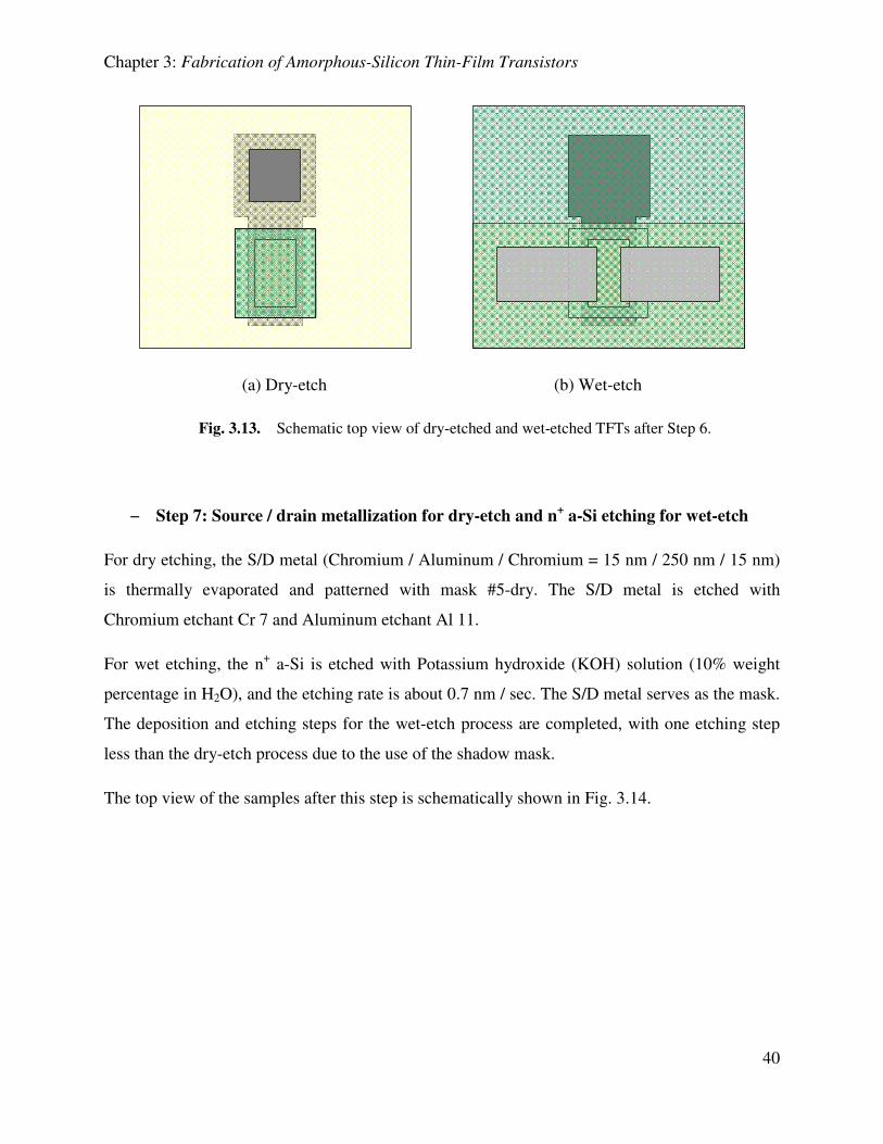
Chapter 3: Fabrication of Amorphous-Silicon Thin-Film Transistors
40
(a) Dry-etch (b) Wet-etch
Fig. 3.13. Schematic top view of dry-etched and wet-etched TFTs after Step 6.
− Step 7: Source / drain metallization for dry-etch and n+ a-Si etching for wet-etch
For dry etching, the S/D metal (Chromium / Aluminum / Chromium = 15 nm / 250 nm / 15 nm)
is thermally evaporated and patterned with mask #5-dry. The S/D metal is etched with
Chromium etchant Cr 7 and Aluminum etchant Al 11.
For wet etching, the n+ a-Si is etched with Potassium hydroxide (KOH) solution (10% weight
percentage in H2O), and the etching rate is about 0.7 nm / sec. The S/D metal serves as the mask.
The deposition and etching steps for the wet-etch process are completed, with one etching step
less than the dry-etch process due to the use of the shadow mask.
The top view of the samples after this step is schematically shown in Fig. 3.14.

Chapter 3: Fabrication of Amorphous-Silicon Thin-Film Transistors
41
(a) Dry-etch (b) Wet-etch (done)
Fig. 3.14. Schematic top view of dry-etched and wet-etched TFTs after Step 7.
− Step 8: n+ a-Si etching for dry-etch
For wet etching, the n+ a-Si is etched with CCl2F2 / O2 plasma. The S/D metal serves as the
mask. During RIE, CCl2F2 = 70 sccm, O2 = 10 sccm, gas pressure = 100 mTorr and RF power =
100W. The etching rate is ~0.05 nm / sec. The deposition and etching steps for the dry-etch
process are now completed.
Dry-etch (done)
Fig. 3.15. Schematic top view of dry-etched TFTs after Step 8.

Chapter 3: Fabrication of Amorphous-Silicon Thin-Film Transistors
42
3.3 Comparison of dry-etch and wet-etch processes
Dry-etch and wet-etch fabrication processes have the same deposition steps. There are four
plasma etching steps in dry-etch fabrication process, which were replaced with wet-etching
methods for wet-etched a-Si TFTs (Table 3-I). The wet-etch process has one etching step less
than the dry-etch process due to the use of the shadow mask.
Table 3-I. Comparison of dry-etching and wet-etching steps
Plasma etching Step in dry-etching
Dry-etching Wet-etching
Mask Etchant Mask Etchant
1 Passivation SiNx etch Photoresist Plasma Photoresist HF
2 Channel a-Si etch Photoresist Plasma Passivation SiNx KOH
3 n+ a-Si etch Photoresist Plasma S/D Cr KOH
4 Gate SiNx via etch Photoresist Plasma Shadow mask N/A

Chapter 3: Fabrication of Amorphous-Silicon Thin-Film Transistors
43
References:
[1] R. A. Street, Hydrogenated amorphous silicon. Cambridge ; New York: Cambridge
University Press, 1991.
[2] J. C. Knights and G. Lucovsky, "Hydrogen in Amorphous-Semiconductors," Crc Critical
Reviews in Solid State and Materials Sciences, vol. 9, pp. 211-283, 1980.
[3] A. Flewitt and A. Nathan, "Thin-Film Silicon Materials and Devices for Large-Area and
Flexible Solar Cells and Electronics," presented at the Materials Research Society
Symposium A Tutorial Program, San Fancisco, CA, 2010.
[4] J. Robertson, "Growth Processes of Hydrogenated Amorphous Silicon," Materials
Reseach Society Symposium Proceedings, vol. 609, pp. A1.4.1-A1.4.12, 2000.
[5] A. Matsuda, K. Nomoto, Y. Takeuchi, A. Suzuki, A. Yuuki, and J. Perrin, "Temperature-
Dependence of the Sticking and Loss Probabilities of Silyl Radicals on Hydrogenated
Amorphous-Silicon," Surface Science, vol. 227, pp. 50-56, Mar 1990.
[6] J. Perrin, M. Shiratani, P. Kae-Nune, H. Videlot, J. Jolly, and J. Guillon, "Surface
reaction probabilities and kinetics of H, SiH3, Si2H5, CH3, and C2H5 during deposition
of a-Si : H and a-C : H from H-2, SiH4, and CH2 discharges," Journal of Vacuum
Science & Technology a-Vacuum Surfaces and Films, vol. 16, pp. 278-289, Jan-Feb
1998.
[7] I. D. French, S. C. Deane, D. T. Murley, J. Hewett, I. G. Gale, and M. J. Powell, "The
Effect of the Amorphous Silicon Alpha-Gamma Transition on Thin Film Transistor
Performance," Materials Reseach Society Symposium Proceedings, vol. 467, pp. 875-
880, 1997.
[8] P. R. I. Cabarrocas, Y. Bouizem, and M. L. Theye, "Defect Density and Hydrogen-
Bonding in Hydrogenated Amorphous-Silicon as Functions of Substrate-Temperature and
Deposition Rate," Philosophical Magazine B-Physics of Condensed Matter Statistical
Mechanics Electronic Optical and Magnetic Properties, vol. 65, pp. 1025-1040, May
1992.
[9] W. Beyer, "Incorporation and thermal stability of hydrogen in amorphous silicon and
germanium," Journal of Non-Crystalline Solids, vol. 200, pp. 40-45, May 1996.
[10] S. Yamasaki, "Optical-Absorption Edge of Hydrogenated Amorphous-Silicon Studied by
Photoacoustic-Spectroscopy," Philosophical Magazine B-Physics of Condensed Matter
Statistical Mechanics Electronic Optical and Magnetic Properties, vol. 56, pp. 79-97, Jul
1987.
[11] J. Perrin, "Plasma and Surface-Reactions during a-Si-H Film Growth," Journal of Non-
Crystalline Solids, vol. 137, pp. 639-644, Dec 1991.
[12] R. B. Wehrspohn, S. C. Deane, I. D. French, I. Gale, J. Hewett, M. J. Powell, and J.
Robertson, "Relative importance of the Si-Si bond and Si-H bond for the stability of
amorphous silicon thin film transistors," Journal of Applied Physics, vol. 87, pp. 144-
154, Jan 1 2000.
[13] D. L. Smith, A. S. Alimonda, C. C. Chen, S. E. Ready, and B. Wacker, "Mechanism of
Sinxhy Deposition from Nh3-Sih4 Plasma," Journal of the Electrochemical Society, vol.
137, pp. 614-623, Feb 1990.
[14] B. L. Jones, "High-Stability, Plasma Deposited, Amorphous-Silicon Nitride for Thin-
Film Transistors," Journal of Non-Crystalline Solids, vol. 77-8, pp. 957-960, Dec 1985.

Chapter 3: Fabrication of Amorphous-Silicon Thin-Film Transistors
44
[15] N. Lustig and J. Kanicki, "Gate Dielectric and Contact Effects in Hydrogenated
Amorphous Silicon-Silicon Nitride Thin-Film Transistors," Journal of Applied Physics,
vol. 65, pp. 3951-3957, May 15 1989.
[16] T. Makino and M. Maeda, "Bonds and Defects in Plasma-Deposited Silicon-Nitride
Using Sih4-Nh3-Ar Mixture," Japanese Journal of Applied Physics Part 1-Regular
Papers Short Notes & Review Papers, vol. 25, pp. 1300-1306, Sep 1986.
[17] A. K. Sinha and T. E. Smith, "Electrical-Properties of Si-N Films Deposited on Silicon
from Reactive Plasma," Journal of Applied Physics, vol. 49, pp. 2756-2760, 1978.
[18] D. Murley, I. French, S. Deane, and R. Gibson, "The effect of hydrogen dilution on the
aminosilane plasma regime used to deposit nitrogen-rich amorphous silicon nitride,"
Journal of Non-Crystalline Solids, vol. 198, pp. 1058-1062, May 1996.
[19] D. T. Murley, R. A. G. Gibson, B. Dunnett, A. Goodyear, and I. D. French, "Influence of
Gas Residence Time on the Deposition of Nitrogen-Rich Amorphous-Silicon Nitride,"
Journal of Non-Crystalline Solids, vol. 187, pp. 324-328, Jul 1995.
[20] S. M. GadelRab, A. M. Miri, and S. G. Chamberlain, "A comparison of the performance
and reliability of wet-etched and dry-etched alpha-Si : H TFT's," Ieee Transactions on
Electron Devices, vol. 45, pp. 560-563, Feb 1998.
[21] A. M. Miri and S. G. Chamberlain, "A Totally Wet Etch Fabrication Technology for
Amorphous Silicon Thin Film Transistors," Materials Reseach Society Symposium
Proceedings, vol. 377, pp. 737-742, 1995.

Chapter 4: Two-Stage Model for Lifetime Prediction of Highly Stable a-Si TFTs
45
Two-Stage Model for Lifetime Prediction of Highly Stable a-Si TFTs
In n-channel amorphous-silicon thin-film transistors (a-Si TFTs), the threshold voltage increases
under positive gate bias, leading to the decreased drain current. As pointed out in Chapter 1, this
instability issue in the a-Si TFT hinders its further application in large area electronics. This
chapter first discusses the modeling for two instability mechanisms in a-Si TFTs – defect
creation in a-Si and charge trapping in the gate silicon nitride (SiNx). Then a two-stage model is
presented for the reliability characterization and lifetime prediction of highly stable a-Si TFTs
under low gate-field stress.
Two stages of the threshold voltage shift are identified from the decrease of the drain saturation
current under low gate-field stress. The first initial stage dominates up to hours or days near
room temperature and it can be characterized with a stretched-exponential model. The second
stage dominates in the long term and then saturates, corresponding to the breaking of weak bonds
in a-Si. It can be modeled with a “unified stretched exponential fit,” in which a thermalization
energy is used to unify experimental measurements of drain current decay at different
temperatures into a single curve.
4.1. Instability mechanisms in a-Si TFTs
It is well established that two mechanisms can be responsible for the instability corresponding to
the threshold voltage rise: (i) defect creation in a-Si [1-3], and (ii) charge trapping in the gate
SiNx [4-8]. In mechanism (i) [1], channel electrons induce the weak Si-Si bonds to break and
form dangling bonds, which then trap electrons and become negatively charged. In mechanism
(ii) [8], channel electrons which leak into the gate silicon-nitride (SiNx) are captured by traps in
the SiNx. As we review below, the threshold shift vs. time caused by these two mechanisms can
both be characterized by a “stretched exponential expression” [1, 8].
4.1.1 Modeling defect creation in a-Si
Electrons in the channel induce weak Si-Si bonds to break into dangling bonds (Fig. 4.1). This
process is reversible unless the dangling bonds relax into stable configurations. Two alternative
models explain this defect relaxation kinetics – hydrogen-diffusion-controlled defect-relaxation
(HCR) and defect-controlled defect-relaxation (DCR). In the HCR model, a hydrogen atom
Chapter 4

Chapter 4: Two-Stage Model for Lifetime Prediction of Highly Stable a-Si TFTs
46
diffuses to the site, attaches itself to one of the dangling bonds, and thereby separates the two
dangling bonds [9-11]. In the DCR model, the two dangling bonds relax locally without the aid
of a diffusing atom [12].
Fig. 4.1. Defect creation in a-Si [13].
− Modeling threshold voltage shift
In the DCR model, defect creation in a-Si is modeled as a transition in energy from an initial
weak bond state to stabilized but metastable dangling bond states [12]. In the two-level
configuration coordinate diagram (Fig. 4.2), state A is the weak bond state and state B is the
dangling bond state.
Fig. 4.2. Two-level configuration coordinate diagram for metastability in a-Si. State A represents
the weak bond state, and state B represents the dangling bond state. E� is the barrier-breaking
energy.
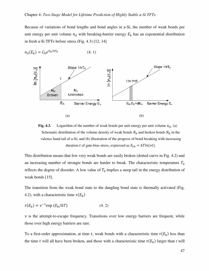
Chapter 4: Two-Stage Model for Lifetime Prediction of Highly Stable a-Si TFTs
47
Because of variations of bond lengths and bond angles in a-Si, the number of weak bonds per
unit energy per unit volume �� with breaking-barrier energy �� has an exponential distribution
in fresh a-Si TFTs before stress (Fig. 4.3) [12, 14]
������ = �� �/��� (4. 1)
(a) (b)
Fig. 4.3. Logarithm of the number of weak bonds per unit energy per unit volume n�. (a)
Schematic distribution of the volume density of weak bonds �� and broken bonds �� in the
valence band tail of a-Si; and (b) illustration of the progress of bond breaking with increasing
duration � of gate-bias stress, expressed as ��� = ��������.
This distribution means that few very weak bonds are easily broken (dotted curve in Fig. 4.2) and
an increasing number of stronger bonds are harder to break. The characteristic temperature ��
reflects the degree of disorder. A low value of �� implies a steep tail in the energy distribution of
weak bonds [15].
The transition from the weak bond state to the dangling bond state is thermally activated (Fig.
4.2), with a characteristic time �����
����� = � !exp ���/��� (4. 2)
� is the attempt-to-escape frequency. Transitions over low energy barriers are frequent, while
those over high energy barriers are rare.
To a first-order approximation, at time �, weak bonds with a characteristic time ����� less than
the time � will all have been broken, and those with a characteristic time ����� larger than t will

Chapter 4: Two-Stage Model for Lifetime Prediction of Highly Stable a-Si TFTs
48
not yet have been broken. This statement can also be expressed in terms of a “thermalization
energy” ��� [16], which is defined as��� ≡ ��ln���� (4. 3)
At time t, we can approximate that weak bonds with a barrier energy �� less than ��� will have
been broken and the stronger bonds above ��� will be intact (Fig. 4.3 (a)). It follows that
between time � and � + (� bonds with barrier energies between ��� and ��� + (��� will break
(the shaded region in Fig. 4.3(b)).
Defining ����� as the number of broken bonds per unit volume, the defect creation rate is
then)*+���
)� = )*+) ,-
) ,-)� (4. 4)
The area of the shaded region in Fig. 4.3(b) is
d������� = �������d��� (4. 5)
Because one weak bond breaks into two dangling bonds, we have d������� = 2d�������. Here
we relate the weak bond states to the created dangling bond states with a ratio of 1 : 2.
Thus the defect creation rate with thermalization energy is
)*+) ,- = 2������� = 2�� ,-/��� (4. 6)
Combined with (4. 2), the defect creation rate is
)*+���)� = )*+
) ,-) ,-
)� = 2��������� ��⁄ ! (4. 7)
Experiments show that the defect creation rate increases with the applied gate voltage 123 [17,
18]. Often the defect creation rate is assumed to be proportional to the number of channel
electrons per unit volume �4� [12, 18], because electrons induce the weak bond to break [12, 16,
18, 19]. After factoring the electron volume density �4� into (4. 7), the defect creation rate as a
function of time becomes
)*+���)� = !�4������������ ��⁄ ! (4. 8)
! is a new constant.

Chapter 4: Two-Stage Model for Lifetime Prediction of Highly Stable a-Si TFTs
49
Because channel electrons are captured by the dangling bonds and raise the threshold voltage,
the threshold voltage is related to the number of dangling bonds per unit volume by
1���� = 5 6 �����d7 /89: (4. 9)
89: is the capacitance of the gate SiNx and the integration is along the channel thinkness 7. Here
we assume that the defects in the a-Si are created very close to the SiNx / a-Si interface. At
constant gate-source bias 123, we have
6 �4����d7 = 89:;123 − 1����=/5 (4. 10)
Substituting (4. 9) and (4. 10) into (4. 8) leads to a stretched exponential expression for the
threshold voltage shift vs. time
∆1���� = 1���� − 1�� = �123 − 1��� ?1 − exp A− B �CDEFGH � IJ,/��� K
�/��LM (4. 11)
1�� is the initial threshold voltage before the application of gate bias, and the activation energy
�N4� = −���ln�!����.
To simplify the formulation of (4. 11), we define
∆1�ONP ≡ 123 − 1�� (4. 12)
because in a given experiment ∆1� cannot exceed 123 − 1�� ,
�� ≡ � !exp ��N4�/��� (4. 13)
and
Q ≡ �/�� (4. 14)
Which leads to (4. 15)
∆1���� = ∆1�ONP ?1 − exp A− B ���KRLM (4. 15)
Q is the ratio of �� to the characteristic energy of the distribution of the weak bonds and Q
decreases as the distribution broadens.
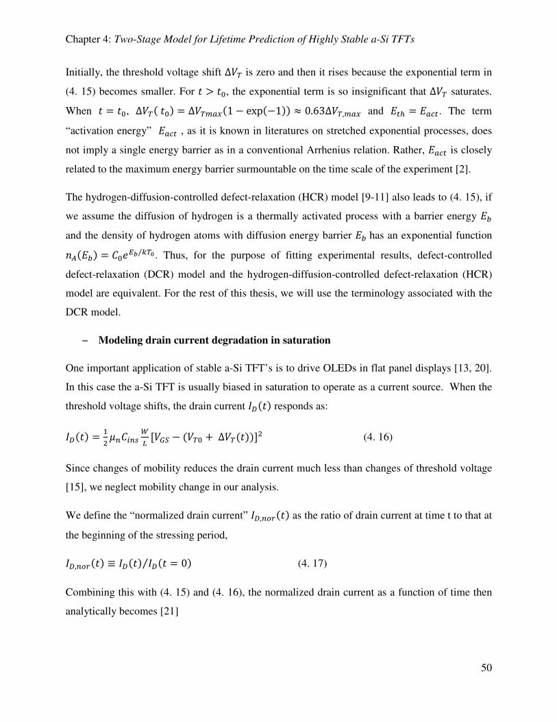
Chapter 4: Two-Stage Model for Lifetime Prediction of Highly Stable a-Si TFTs
50
Initially, the threshold voltage shift ∆1� is zero and then it rises because the exponential term in
(4. 15) becomes smaller. For � > ��, the exponential term is so insignificant that ∆1� saturates.
When � = ��, ∆1�� ��� = ∆1�ONP�1 − exp�−1�� ≈ 0.63∆1�,ONP and ��� = �N4�. The term
“activation energy” �N4� , as it is known in literatures on stretched exponential processes, does
not imply a single energy barrier as in a conventional Arrhenius relation. Rather, �N4� is closely
related to the maximum energy barrier surmountable on the time scale of the experiment [2].
The hydrogen-diffusion-controlled defect-relaxation (HCR) model [9-11] also leads to (4. 15), if
we assume the diffusion of hydrogen is a thermally activated process with a barrier energy ��
and the density of hydrogen atoms with diffusion energy barrier �� has an exponential function
������ = �� �/��� . Thus, for the purpose of fitting experimental results, defect-controlled
defect-relaxation (DCR) model and the hydrogen-diffusion-controlled defect-relaxation (HCR)
model are equivalent. For the rest of this thesis, we will use the terminology associated with the
DCR model.
− Modeling drain current degradation in saturation
One important application of stable a-Si TFT’s is to drive OLEDs in flat panel displays [13, 20].
In this case the a-Si TFT is usually biased in saturation to operate as a current source. When the
threshold voltage shifts, the drain current Z[��� responds as:
Z[��� = !\ ]989: ^
_ ;123 − �1�� + ∆1�����=\ (4. 16)
Since changes of mobility reduces the drain current much less than changes of threshold voltage
[15], we neglect mobility change in our analysis.
We define the “normalized drain current” Z[,9`a��� as the ratio of drain current at time t to that at
the beginning of the stressing period,
Z[,9`a��� ≡ Z[��� Z[�� = 0�⁄ (4. 17)
Combining this with (4. 15) and (4. 16), the normalized drain current as a function of time then
analytically becomes [21]
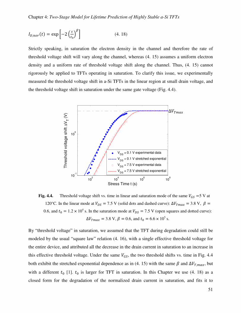
Chapter 4: Two-Stage Model for Lifetime Prediction of Highly Stable a-Si TFTs
51
Z[,9`a��� = exp A−2 B ���KRL (4. 18)
Strictly speaking, in saturation the electron density in the channel and therefore the rate of
threshold voltage shift will vary along the channel, whereas (4. 15) assumes a uniform electron
density and a uniform rate of threshold voltage shift along the channel. Thus, (4. 15) cannot
rigorously be applied to TFTs operating in saturation. To clarify this issue, we experimentally
measured the threshold voltage shift in a-Si TFTs in the linear region at small drain voltage, and
the threshold voltage shift in saturation under the same gate voltage (Fig. 4.4).
Fig. 4.4. Threshold voltage shift vs. time in linear and saturation mode of the same 123 =5 V at
120°C. In the linear mode at 1[3 = 7.5 V (solid dots and dashed curve): ∆1�ONP = 3.8 V, Q =
0.6, and �� = 1.2 × 10⁴ s. In the saturation mode at 1[3 = 7.5 V (open squares and dotted curve):
∆1�ONP = 3.8 V, Q = 0.6, and �� = 6.6 × 10⁵ s.
By “threshold voltage” in saturation, we assumed that the TFT during degradation could still be
modeled by the usual “square law” relation (4. 16), with a single effective threshold voltage for
the entire device, and attributed all the decrease in the drain current in saturation to an increase in
this effective threshold voltage. Under the same 123, the two threshold shifts vs. time in Fig. 4.4
both exhibit the stretched exponential dependence as in (4. 15) with the same Q and ∆1�,ONP, but
with a different �� [1]. �� is larger for TFT in saturation. In this Chapter we use (4. 18) as a
closed form for the degradation of the normalized drain current in saturation, and fits it to
102
104
106
108
10-1
100
Stress Time t (s)
Th
resh
old
vo
ltag
e s
hift
∆V
T (
V)
VDS
= 0.1 V experimental data
VDS
= 0.1 V stretched exponential
VDS
= 7.5 V experimental data
VDS
= 7.5 V stretched exponential
∆1�ONP

Chapter 4: Two-Stage Model for Lifetime Prediction of Highly Stable a-Si TFTs
52
experimental measurements in Section 4.3. In Chapter 7, the dependence of drain current
degradation and threshold voltage shift on the drain-bias will be addressed in detail.
4.1.2 Modeling charge trapping in the gate SiNx
When channel electrons enter the gate insulator and then are captured by traps there, the
threshold voltage shifts (Fig. 4.5).
Channel Electrons
EC
EV
EFS
e-Nitride Defects
(traps)
EFM
Charge trapping
a-SiSiNxGate
Fig. 4.5. Charge trapping in gate SiNx [13].
If one assumes that all electrons that enter the insulator are trapped, the threshold voltage shift
depends strictly on the process of electron tunneling into the gate insulator, and has a logarithmic
time dependence [5].
∆1���� = bclog �1 + � ��⁄ � (4. 19)
The constant bc contains the density of traps �� [cm-3
] and a tunneling constant f [cm] [5]. This
tunneling mechanism typically dominates at high-gate field (> 106
V/cm) [13, 20] and produces a
weak temperature dependence [5].
On the other hand, if most electrons that enter the gate insulator are not trapped and continue to
the gate electrode, the threshold voltage shift can be shown to follow the stretched exponential
expression as (4. 15) [5, 6, 8, 22]. This expression can be derived by assuming a continuous
distribution in the capture cross section of the trapping sites [8]. The parameters ∆1�ONP , Q and
�� in (4. 15), which characterize charge trapping in the gate SiNx, have physical origins that are
different from those to characterize defect creation in a-Si. When all traps in the SiNx are filled,

Chapter 4: Two-Stage Model for Lifetime Prediction of Highly Stable a-Si TFTs
53
the threshold voltage shift saturates and reaches ∆1�ONP . Thus, the parameter ∆1�ONP =5��`� < ( >/h ∙ jb�j, where ��`� is the total density of traps, < ( > is the centroid of trapped
charge measured from the gate metal, and h is the permittivity of the gate SiNx. Q is a measure of
the distribution width of capture cross section, with a value between 0 and 1. Q decreases as the
distribution broadens, and Q = 1 implies a single trap cross section. In principle, the
characteristic time t� can be determined from the gate leakage current and characteristic capture
cross section for the ensemble of traps [8]. In practice, �� is determined from (4. 15) as the time
when ∆1� = 0.63 ∆1�ONP. Because gate leakage current and capture cross section may depend
on temperature [8], the threshold voltage shift also may depend on temperature.
The above charge-trapping model, based on continuous distribution in trapping capture cross
section, was first derived to explain the threshold voltage shift in single crystalline Si field-effect
transistors with high permittivity dielectric gate insulator, such as Al2O3 and HfO2. When applied
to a-Si TFTs with SiNx gate insulator, the stretched exponential form of (4. 15) has also results in
good fits to experimental data, although without connecting to an explicit physical model.
4.1.3 Summary of instability models for a-Si TFTs
A conclusion from the previous two sections is that the stretched exponential expression (4. 15)
can be used to model the threshold voltage shift caused by either defect creation in a-Si or charge
trapping in the gate SiNx. The model requires three parameters ∆1�ONP, Q and ��, which are
listed in Table 4-I. They are used to describe the threshold voltage shift vs. time at a given
temperature. It is difficult to determine which instability mechanism is operating in a-Si TFTs
from simply observing the threshold voltage shift [22]. However as noted in Section 4.1.1, for
defect creation in a-Si, we expect ∆1�ONP = 123 − 1��, while for charge trapping in SiNx,
∆1�ONP could be less than 123 − 1�� if the number of traps in the gate insulator is small. Such an
observation in practice would allow one to differentiate between the two instability mechanisms.
Furthermore, defect spectroscopy techniques [23] would allow one to observe the newly created
defect states in a-Si. In Chapter 6, field-effect technique proves that defect creation occurs in a-Si
TFTs under low gate-field.
Table 4-I. Stretched exponential expression for instability mechanisms in a-Si TFTs

Chapter 4: Two-Stage Model for Lifetime Prediction of Highly Stable a-Si TFTs
54
∆1���� = ∆1�ONP l1 − exp m− n ���oRpq
Parameter Defect creation in a-Si (Stage II) Charge trapping in gate SiNx (Stage I)
∆1�ONP 123 − 1�� 5��`� < ( >/h ∙ jb�j
Q A measure of the distribution of
barrier energy �� with Q = �/��
A measure of width of the distribution of
the capture cross section 0 ≤ Q ≤ 1
�� Time scale to reach ∆1�,ONP .
Depends on the attempt-to-escape
frequency �, activation energy �N4�,
and temperature �, with �� =� !exp��N4�/���
Time scale to reach ∆1�,ONP . Depends
on the gate leakage current and
characteristic capture cross section
4.2. Sample preparation and bias-temperature-stress measurement
Highly stable a-Si TFTs were fabricated with a standard bottom-gate non-self-aligned process in
the back-channel passivated (BCP) structure. The silicon nitride and amorphous silicon were
deposited in a plasma-enhanced chemical vapor deposition (PECVD) system. 300-nm gate
nitride, 200-nm intrinsic hydrogenated a-Si and 300-nm passivation nitride were deposited
sequentially at 320°C, 320°C and 220°C, respectively. A dry-etching process as described in
Chapter 3 was performed to pattern the silicon nitride and a-Si. All the samples were annealed at
180°C for an hour to remove the plasma-induced damage from the dry-etching process [15].
After annealing, the initial threshold voltage 1�� was 1.0 V and electron mobility ]9 was 0.9
cm2/V·s.
The TFTs were biased in the saturation mode with a constant gate voltage of 5 V (a gate field of
~1.5 × 10⁵
V/cm) and a constant drain voltage of 7.5 V. Saturation, as opposed to linear mode,
was used because this mode of operation is used for driving OLEDs, an application which
demands very high stability [13]. We raised the substrate temperature from 20°C to 140°C in
steps of 20°C. At each temperature we biased a fresh TFT on the same substrate without any
prior stress and again measured the drain current as a function of time. At the end of the
continuous bias stress period, a gate-bias voltage sweep and fixed drain voltage were applied to

Chapter 4: Two-Stage Model for Lifetime Prediction of Highly Stable a-Si TFTs
55
measure the Z[ - 12 characteristics of the TFTs [15]. This allowed us to measure the mobility of
the TFT at the end of the stress period. The experimental data of normalized drain current
Z[,9`a��� ≡ Z[���/Z[�� = 0� as a function of time at different temperatures are shown with open
squares in Fig. 4.6.
Fig. 4.6. Single stretched exponential fits to normalized drain current data at temperatures from
20°C to 140°C in steps of 20°C.
4.3. Two-stage model for lifetime prediction
It has been shown that defect creation in a-Si and charge trapping in the gate SiNx can both be
modeled with a stretched exponential expression with a stretched exponential expression. In this
section, single stretched-exponential fit is tried to model the drain current degradation first. Next,
a “unified stretched exponential fit” to the drain current degradation caused by defect creation in
a-Si is proposed. The unified stretched exponential fit agrees well with the experimental data in
the temperature range from 80°C to 140°C. At lower temperatures (20°C to 60°C), the drain
current degradation approaches the model only at long times. A different instability mechanism
contributes in the beginning (Stage I), in addition to the unified stretched exponential model
(Stage II). By subtracting the threshold voltage shift of the unified stretched exponential fit from
the total threshold voltage shift data, we identify and characterize the Stage I.
100
102
104
106
108
1010
0
0.2
0.4
0.6
0.8
1
Stress Time t (s)
No
rma
lize
d D
rain
Cu
rre
nt I D
,nor
Experimental data
Single stretched exponential
20°C 140°C

Chapter 4: Two-Stage Model for Lifetime Prediction of Highly Stable a-Si TFTs
56
4.3.1 Single stretched-exponential fit
Fig. 4.6 shows that at 5 V gate bias, the drain current approaches zero at long times and depends
strongly on temperature. We fit the stretched exponential expression of (4. 15) for defect creation
in a-Si to the experimental data for each temperature (dotted curves in Fig. 4.6). Each
temperature requires separate fitting parameters �� ≡ �/Q and ��, which are plotted in Fig. 4.7
and Fig. 4.8, respectively.
Fig. 4.7 shows that the characteristic temperature �� of the defect energy distribution changes
from 1032 K at 20°C to 616 K at 140°C, and that it decreases rapidly in low temperature range.
Similar results were reported in [6, 21]. From the slope of the Arrhenius plot of log �� (straight
line in Fig. 4.8), the activation energy �N4� = 0.89 eV and the attempt-to-escape frequency � = 4
× 106 Hz are extracted from (4. 13) �� ≡ � !exp ��N4�/���. However, the experimental �� at
low temperatures does not fall on the straight line.
From the discussion of instability in a-Si of Section 4.1.1, the anomalously large �� and �� near
room temperature result from either changes in material properties with temperature, or a single
stretched exponential fit not being appropriate for the entire temperature range. In Section 4.3.4,
we will show that material properties do not change. Another instability mechanism relevant near
room temperature for short time makes the single stretched exponential fit inadequate.
280 300 320 340 360 380 400 420500
600
700
800
900
1000
1100
Stress Temperature T (K)
Ch
ara
cte
ristic T
em
pe
ratu
re T
0 (
K)

Chapter 4: Two-Stage Model for Lifetime Prediction of Highly Stable a-Si TFTs
57
Fig. 4.7. Fitting parameter characteristic temperature �� as a function of bias stressing
temperature.
Fig. 4.8. Fitting parameter characteristic time t� as a function of reciprocal temperature in an
Arrhenius plot. �N4� = 0.89 eV and � = 4 × 10⁶ Hz.
4.3.2 Unification of time and temperature
If the instability is caused by defect creation in a-Si and the material properties do not change
with temperature, it can be captured with a formulation that unifies time and temperature
dependence. The definition of the thermalization energy ��� of (4. 3) implies that the time scale
can be converted to the ��� scale. Doing that enables reducing all sets of current vs. time data for
different temperatures to a single curve [16]. As discussed in Section 4.1.1, for a given
thermalization energy a given number of bonds has been broken, leading to a specified change in
threshold voltage and drain current. As time � advances and weak bonds with higher barrier
energy �� are broken, the thermalization energy ��� increases. Schematically, this is represented
by an increase to the area of the shaded region in Fig. 4.3(a). Temperature affects only how long
it takes to reach a given thermalization energy.
When � is set to be 5 × 10⁶
Hz, all experimental data on drain current degradation from 20°C to
140°C cluster as shown by the open squares in Fig. 4.9.
2.2 2.4 2.6 2.8 3.0 3.2 3.4 3.610
2
104
106
108
1010
1012
Reciprocal Temperature 1000/T (1/K)
Ch
ara
cte
ristic
Tim
e t 0 (
s)
140 120 100 80 60 40 20

Chapter 4: Two-Stage Model for Lifetime Prediction of Highly Stable a-Si TFTs
58
Fig. 4.9. Normalized drain current Z[,9`a unified in terms of the thermalization energy ��� =��ln����, with � = 5 × 10
6 Hz, and unified stretched exponential fit with parameters �N4� = 0.90
eV and �� = 643 K (solid curve). Dash dotted curves are unified stretched exponential models at
different �N4� or ��, to show the effect on Z[,9`a.
The fitting parameter � is close to that obtained from Fig. 4.8 of 4 × 10⁶
Hz. This agreement
suggests that the material properties remain essentially unchanged between 20°C and 140°C in
our experiment. This observation gives us confidence for applying the unified stretched
exponential fit to drain current degradation that follows.
4.3.3 Unified stretched exponential fit (Stage II model)
By substituting (4. 3) ��� = ��ln����, (4. 13) �� = exp ��N4�/���, and (4. 14) Q = �/�� into
(4. 18), we obtain the unified stretched exponential expression for Z[,9`a as a function of
thermalization energy ���
Z[,9`a����� = exp s−2exp t ,- IJ,��� uv (4. 20)
The activation energy �N4� is the barrier energy for defect creation when the normalized drain
current has droped to e \ ≈ 0.135. As discussed in Section 4.1.1, �N4� is related to the
maximum energy barrier surmountable on the time scale of the experiment [2]. Note that this
unified stretched exponential expression is independent of temperature.
0.3 0.4 0.5 0.6 0.7 0.8 0.9 1 1.10
0.2
0.4
0.6
0.8
1
Thermalization Energy Eth
(eV)
No
rma
lize
d D
rain
Cu
rre
nt I D
,nor
Experimental data
Unified stretched exponential
�N4� = 0.80 eV
�N4�
�� = 900 K

Chapter 4: Two-Stage Model for Lifetime Prediction of Highly Stable a-Si TFTs
59
The solid curve in Fig. 4.9 shows that (4. 20) provides an excellent fit to the clustered data. The
fitting parameters are �N4� = 0.90 eV and �� = 643 K, which are typical values for a-Si [19].
The dash-dotted curves in Fig. 4.9 are plotted for �N4� = 0.80 eV and �� = 900 K to show the
effect of varying �N4� and �� on the curve fit. Varying the activation energy �N4� is seen to shift
the current degradation, while varying the characteristic temperature �� affects the slope.
The relation of ��� = ��ln���� between thermalization energy and time enables plotting
stretched exponential fits in a direct function of time as shown by dotted curves in Fig. 4.10. The
experimental data fit well at high temperatures from 80°C to 140°C. At low temperatures, the
experimental drain currents degradation lie below the unified stretched exponential fit at short
times, but trend toward the unified stretched exponential fit at long times. These observations
suggest that an additional instability mechanism causes the drain current to drop at the beginning
of the tests. This initial instability mechanism, which is manifest at low temperatures and short
times, requires an additional physical model.
Fig. 4.10. Unified stretched exponential fits (Stage II) vs. stress times to experimental data from
20°C to 140°C in steps of 20°C, with fitting parameters � = 5 × 10⁶ Hz, �N4� = 0.9 eV and �� =
643 K.
100
102
104
106
108
1010
0
0.2
0.4
0.6
0.8
1
Stress Time t (s)
No
rma
lize
d D
rain
Cu
rre
nt I D
,nor
Experimental data
Unified stretched exponential
20°C 140°C

Chapter 4: Two-Stage Model for Lifetime Prediction of Highly Stable a-Si TFTs
60
4.3.4 Two-stage model
In order to model the initial additional instability at low temperatures, we define the threshold
voltage shift caused by the initial instability mechanism as ∆1�,y��� (Stage I), and add it to the
long-term threshold voltage shift characterized by the unified stretched exponential model
∆1�,yy��� (Stage II), to obtain the total threshold voltage shift ∆1�,�`�Nz���
∆1�,�`�Nz��� = ∆1�,y��� + ∆1�,yy��� (4. 21)
We first analyze the threshold voltage shift at 20⁰C, where the initial instability is most
pronounced. Fig. 4.11 shows the experimental data points and model fits at 20°C. Open squares
are the experimental data for ∆1�,�`�Nz��� extracted from the measured drain current data using
(4. 16). The dotted curve in Fig. 4.11 is from the unified stretched exponential fit in Section
4.3.3., that is now referred as the Stage II model. At long times, the Stage II model approaches
the experimental data. However, at short times (< 103
seconds), a fast initial mechanism makes
the threshold voltage shift rise above the unified stretched exponential fit. Stage I degradation
saturates at the maximum threshold voltage shift ∆1�ONP,y, which is marked in Fig. 4.11.
∆1�,yy��� for Stage II is obtained from (4. 15) with ∆1�ONP,yy = 123 − 1�� − ∆1�ONP,y. By
subtracting ∆1�,yy��� from the total threshold voltage shift vs. time data, ∆1�,y��� is obtained.
While the mechanism of Stage I is not known, we fit the ∆1�,y��� data also with the stretched
exponential expression (4. 15).
100
105
1010
10-2
10-1
100
101
Stress Time t (s)
Th
resh
old
Vo
ltag
e S
hift ∆
VT (
V)
Experimental data
Stage II model
Data "minus" Stage II model
Stage I model
Two-stage model
∆1�ONP
∆1�ONP,y
� =20°C

Chapter 4: Two-Stage Model for Lifetime Prediction of Highly Stable a-Si TFTs
61
Fig. 4.11. Two-stage model fits to threshold voltage shift vs. time at 20°C (dashed curve, overlaps
with Stage I curve at lower left and overlaps with Stage II curve at upper right). The dots for
Stage I “data” result from subtracting the Stage II model (determined by high temperature
experiments) from the experimental data. The fitting parameters for Stage I are ∆1�ONP,y = 0.08
V, ��,y = 0.7 sec and Qy = 0.15; and for Stage II are ��,yy = 5.2 × 10⁸ sec and Qyy = 0.46.
From Section 4.3.3, the fitting parameters are � = 5 × 10⁶
Hz, �N4� = 0.9 eV and �� = 643 K,
corresponding to ��,yy = 5.2 × 10⁸
sec and Qyy = 0.46 at 20⁰C for Stage II. In Fig. 4.11, we choose
∆1�ONP,y = 0.08 V. ∆1�,y��� is plotted with solid dots and saturates at 0.08 V. It means the
choice of ∆1�ONP,y = 0.08 V is proper. Taking the empirical approach, we find that ∆1�,y��� can
be fitted with the stretched exponential model (4. 15) with the parameters ∆1�ONP,y = 0.08 V,
��,y = 0.7 sec and Qy = 0.15, shown with the dash-dotted curve in Fig. 4.11. The two-stage fit of
the dashed curve then is obtained by adding Stage I fit and Stage II fit. The result agrees well
with the experimental data taken at 20⁰C over the entire measurement time.
We also applied the two-stage model to the experimental data taken at temperatures from 40°C
to 140°C. The maximum threshold voltage shift in Stage I ∆1�ONP,y varies with temperature as
illustrated in Fig. 4.12.
Fig. 4.12. Maximum threshold voltage shift in Stage I ∆1�ONP,y at temperatures from 20°C to
140°C.
0 20 40 60 80 100 120 140 1600
0.01
0.02
0.03
0.04
0.05
0.06
0.07
0.08
0.09
0.1
Stress Temperature T (oC)
∆V
Tm
ax,
I (V
)

Chapter 4: Two-Stage Model for Lifetime Prediction of Highly Stable a-Si TFTs
62
At high temperatures, it decreases to zero. After converting the threshold voltage back to drain
current via (4. 16), the two-stage fits to the normalized drain current degradation from 20°C to
140°C are shown in Fig. 4.13. The fits agree well with the experimental data at all temperatures
and times, clearly better than the single stretched exponential fits of the dotted curves in Fig. 4.6
or the unified stretched exponential fits (Stage II only) of the dotted curves in Fig. 4.10.
Fig. 4.13. Two-stage model fit to experimental data from 20°C to 140°C in steps of 20°C (dashed
curves), and the single stretched exponential fit at 20°C (dotted curve at right).
4.4. Discussion
− Two-stage model
From Section 4.3, we know that the unified stretched exponential fits Stage II from 80°C to
140°C, but does not agree well with the experimental data at low temperatures from 20°C to
60°C. Fig. 4.12 tells us that the maximum threshold voltage shift in Stage I ∆1ONP,y is negligible
at high temperatures. The reason is that the threshold voltage shift in Stage I occurs so fast that
above 60⁰C the Stage I mechanism has already saturated by the time we took our initial drain
current data point, about 0.1 sec after the gate and drain bias were applied to get the first data
point. Therefore, at elevated temperatures Stage II can be modeled reliable with the unified
stretched exponential, because the effect of Stage I can be neglected. In summary, the unified
100
102
104
106
108
1010
0
0.2
0.4
0.6
0.8
1
Stress Time t (s)
No
rma
lize
d D
rain
Cu
rre
nt I D
,nor
Experimental data
Two-stage model
Single stretched exponential
20°C 140°C

Chapter 4: Two-Stage Model for Lifetime Prediction of Highly Stable a-Si TFTs
63
stretched exponential fit of (4. 19) can be used to model Stage II, and Stage I can be modeled
with the stretched exponential expression of (4. 15). Because Stage I saturates at ∆1�ONP,y noticeable below 123 − 1��, we attribute the instability mechanism of Stage I to charge trapping
in the gate SiNx , where the trap density is grown-in and independent of the density of electrons
in the channel. The threshold voltage shift in Stage II is attributed to defect creation in a-Si,
which is induced by the density of electrons in the channel and therefore rises with rising gate
bias.
The backward process is charge de-trapping for charge trapping and defect annealing for defect
creation. In the presence of the channel electrons, rates of the backward processes are much
lower than the rate of the corresponding forward processes [12, 24]. When the gate voltage is
turned off, the threshold voltage recovers through the backward process. The two-stage model
does not take into account of the backward processes in two stages.
− Prediction of drain current lifetime
At room temperature, the drain current degradation in Stage I is still fast and measured at short
times. The current degradation in Stage II can be predicted from the unified stretched
exponential fit to the experimental data at elevated temperatures. We define the time for the TFT
drain current to drop to x% of its initial value under constant gate voltage bias as x% drain
current lifetime (�P%). The lifetime at room temperature can be predicted from the two-stage
model. Fig. 4.14 demonstrates the 90%, 70% and 50% lifetimes (�|�%, �}�%, �~�%) measured in
our experiment (open squares).
Chapter 4: Two-Stage Model for Lifetime Prediction of Highly Stable a-Si TFTs
64
Fig. 4.14. Time at which the drain current drops to 50%, 70% and 90% of its initial value, in
function of temperature. Open squares: experimental data; dotted lines: Stage II model with
unified stretched exponential fit; solid dots and dashed lines: two-stage model.
The lifetimes extrapolated from only the Stage II model (unified stretched exponential fits,
dotted lines) and the full two-stage model (solid dots and dashed lines). Since the threshold
voltage shift in Stage I of our highly stable a-Si TFTs saturates at no more than 0.1 V, at long
times the threshold voltage shift will be dominated by Stage II. The fitting parameters and the
predicted 50% lifetimes are listed in Table 4-II.
Table 4-II. Fitting parameters and predicted 50% lifetime
Stage I Stage II Two-stage
∆1�ONP,y(V)
��,y (s)
Qy �
(Hz)
��
(K)
�N4�
(eV)
��,yy (s)
Qyy 50% lifetime
(s)
50% lifetime
(s)
0.08 1.1 0.2 5 × 10⁶ 643 0.90 5.2 × 10
8 0.46 5.1 × 10
7 4.5 × 10
7
One conclusion of our work is that gate-bias stress test conducted at 20°C for times shorter than
106 seconds do not accurately predict the long term (Stage II) performance [13, 20, 25]. This
conclusion is illustrated by the discrepancy between the dotted curve and the dashed curve in
Fig. 4.13, both of which fit 20°C data.
2.4 2.6 2.8 3 3.2 3.410
2
103
104
105
106
107
108
Reciprocal Temperature 1000/T (1/K)
Dra
in C
urr
en
t L
ife
time
s (
s)
Experimental data
Stage II model
Two-stage model�~�%
�}�%
�|�%

Chapter 4: Two-Stage Model for Lifetime Prediction of Highly Stable a-Si TFTs
65
In Fig. 4.14, note that the slopes of the Stage II model fit to the 90%, 70% and 50% lifetimes are
different. The differences reflect that no single activation energy applies to the degradation of a-
Si TFTs, in contrast to the conventional Arrhenius model that is applied to the thermal aging of
many other electronic devices.
− Extension to constant current stress
In AMOLED pixel circuits with threshold voltage compensation, the gate voltage increases with
the increasing threshold voltage, so the driver transistors are subject to constant current stressing
[26, 27]. Since 123��� − 1���� is kept constant, from (4. 8) - (4. 10) threshold voltage shift in
Stage II from defect creation follows a power law relationship [28]
∆1���� = ;123��� − 1����= B ���KR
(4. 22)
As in Section 4.3.2, the time scale can be converted to the thermalization energy ��� scale using
(4. 3) ��� = ��ln���� to give
∆1������ = ;123����� − 1������=exp t ,- IJ,��� u (4. 23)
Thus, the room temperature threshold voltage shift in Stage II can be predicted from the
threshold voltage shift at elevated temperatures. Note the electron density and the rate of
threshold voltage shift are assumed to be uniform along the channel. The rigorous non-uniform
channel analysis for TFTs biased in saturation should follow a similar analysis as in Chapter 7.
4.5. Summary and conclusion
We measured and modeled the drain current degradation and threshold voltage shift of a-Si TFTs
under low gate-field stress between 20⁰C and 140⁰C. Over most of the time-temperature range,
the unified stretched exponential model that reflects defect creation in the a-Si channel (Stage II)
applies. Near room temperature, a separate mechanism contributes to TFT degradation. An
empirical fit, with a stretched exponential, suggests that the underling mechanism is the charge
trapping in the SiNx gate insulator (Stage I). While this mechanism makes only a minor
contribution to the overall threshold voltage shift and drain current degradation, it can
considerably falsify TFT lifetimes extrapolated from tests done at room temperature. Because for

Chapter 4: Two-Stage Model for Lifetime Prediction of Highly Stable a-Si TFTs
66
reasonable test duration (~1 month) at room temperature, it is not yet possible to accurately
estimate the parameters which dominate the long term degradation.

Chapter 4: Two-Stage Model for Lifetime Prediction of Highly Stable a-Si TFTs
67
References:
[1] K. S. Karim, A. Nathan, M. Hack, and W. I. Milne, "Drain-bias dependence of threshold
voltage stability of amorphous silicon TFTs," Ieee Electron Device Letters, vol. 25, pp.
188-190, Apr 2004.
[2] M. J. Powell, C. Vanberkel, A. R. Franklin, S. C. Deane, and W. I. Milne, "Defect Pool in
Amorphous-Silicon Thin-Film Transistors," Physical Review B, vol. 45, pp. 4160-4170,
Feb 15 1992.
[3] C. Vanberkel and M. J. Powell, "Resolution of Amorphous-Silicon Thin-Film Transistor
Instability Mechanisms Using Ambipolar Transistors," Applied Physics Letters, vol. 51,
pp. 1094-1096, Oct 5 1987.
[4] M. J. Powell, C. Vanberkel, and J. R. Hughes, "Time and Temperature-Dependence of
Instability Mechanisms in Amorphous-Silicon Thin-Film Transistors," Applied Physics
Letters, vol. 54, pp. 1323-1325, Apr 3 1989.
[5] M. J. Powell, "Charge Trapping Instabilities in Amorphous Silicon-Silicon Nitride Thin-
Film Transistors," Applied Physics Letters, vol. 43, pp. 597-599, 1983.
[6] F. R. Libsch and J. Kanicki, "Bias-Stress-Induced Stretched-Exponential Time-
Dependence of Charge Injection and Trapping in Amorphous Thin-Film Transistors,"
Applied Physics Letters, vol. 62, pp. 1286-1288, Mar 15 1993.
[7] J. Triska, J. F. Conley, R. Presley, and J. F. Wager, "Bias stress stability of zinc-tin-oxide
thin-film transistors with Al2O3 gate dielectrics," Journal of Vacuum Science &
Technology B, vol. 28, pp. C5i1-C5i6, Jul 2010.
[8] S. Zafar, A. Callegari, E. Gusev, and M. V. Fischetti, "Charge trapping related threshold
voltage instabilities in high permittivity gate dielectric stacks," Journal of Applied
Physics, vol. 93, pp. 9298-9303, Jun 1 2003.
[9] M. Stutzmann, W. B. Jackson, and C. C. Tsai, "Light-Induced Metastable Defects in
Hydrogenated Amorphous-Silicon - a Systematic Study," Physical Review B, vol. 32, pp.
23-47, 1985.
[10] J. Kakalios, R. A. Street, and W. B. Jackson, "Stretched-Exponential Relaxation Arising
from Dispersive Diffusion of Hydrogen in Amorphous-Silicon," Physical Review Letters,
vol. 59, pp. 1037-1040, Aug 31 1987.
[11] R. A. Street, C. C. Tsai, J. Kakalios, and W. B. Jackson, "Hydrogen Diffusion in
Amorphous-Silicon," Philosophical Magazine B-Physics of Condensed Matter Statistical
Mechanics Electronic Optical and Magnetic Properties, vol. 56, pp. 305-320, Sep 1987.
[12] R. S. Crandall, "Defect Relaxation in Amorphous-Silicon - Stretched Exponentials, the
Meyer-Neldel Rule, and the Staebler-Wronski Effect," Physical Review B, vol. 43, pp.
4057-4070, Feb 15 1991.
[13] B. Hekmatshoar, K. H. Cherenack, S. Wagner, and J. C. Sturm, "Amorphous silicon thin-
film transistors with DC saturation current half-life of more than 100 years," in Electron
Devices Meeting, 2008. IEDM 2008. IEEE International, 2008, pp. 1-4.
[14] R. B. Wehrspohn, M. J. Powell, and S. C. Deane, "Kinetics of defect creation in
amorphous silicon thin film transistors," Journal of Applied Physics, vol. 93, pp. 5780-
5788, May 1 2003.
[15] T. Liu, S. Wagner, and J. C. Sturm, "A new method for predicting the lifetime of highly
stable amorphous-silicon thin-film transistors from accelerated tests," in Reliability
Physics Symposium (IRPS), 2011 IEEE International, 2011, pp. 2E.3.1-2E.3.5.

Chapter 4: Two-Stage Model for Lifetime Prediction of Highly Stable a-Si TFTs
68
[16] S. C. Deane, R. B. Wehrspohn, and M. J. Powell, "Unification of the time and
temperature dependence of dangling-bond-defect creation and removal in amorphous-
silicon thin-film transistors," Physical Review B, vol. 58, pp. 12625-12628, Nov 15 1998.
[17] W. B. Jackson, "Role of Band-Tail Carriers in Metastable Defect Formation and
Annealing in Hydrogenated Amorphous-Silicon," Physical Review B, vol. 41, pp. 1059-
1075, Jan 15 1990.
[18] W. B. Jackson, J. M. Marshall, and M. D. Moyer, "Role of Hydrogen in the Formation of
Metastable Defects in Hydrogenated Amorphous-Silicon," Physical Review B, vol. 39,
pp. 1164-1179, Jan 15 1989.
[19] R. B. Wehrspohn, S. C. Deane, I. D. French, and M. J. Powell, "Stability of plasma
deposited thin film transistors - comparison of amorphous and microcrystalline silicon,"
Thin Solid Films, vol. 383, pp. 117-121, Feb 15 2001.
[20] B. Hekmatshoar, S. Wagner, and J. C. Sturm, "Tradeoff regimes of lifetime in amorphous
silicon thin-film transistors and a universal lifetime comparison framework," Applied
Physics Letters, vol. 95, Oct 5 2009.
[21] C. C. Shih, Y. S. Lee, K. L. Fang, C. H. Chen, and F. Y. Gan, "A current estimation
method for bias-temperature stress of a-Si TFT device," Ieee Transactions on Device and
Materials Reliability, vol. 7, pp. 347-350, Jun 2007.
[22] A. V. Gelatos and J. Kanicki, "Bias Stress-Induced Instabilities in Amorphous-Silicon
Nitride Hydrogenated Amorphous-Silicon Structures - Is the Carrier-Induced Defect
Creation Model Correct," Applied Physics Letters, vol. 57, pp. 1197-1199, Sep 17 1990.
[23] J. Kanicki, Amorphous and microcrystalline semiconductor devices. Volume II, Materials
and device physics. Boston: Artech House, 1992.
[24] A. A. Fomani and A. Nathan, "Metastability mechanisms in thin film transistors
quantitatively resolved using post-stress relaxation of threshold voltage," Journal of
Applied Physics, vol. 109, Apr 15 2011.
[25] B. Hekmatshoar, K. H. Cherenack, A. Z. Kattamis, K. Long, S. Wagner, and J. C. Sturm,
"Highly stable amorphous-silicon thin-film transistors on clear plastic," Applied Physics
Letters, vol. 93, Jul 21 2008.
[26] A. Nathan, D. Striakhilev, R. Chaji, S. Ashtiani, C.-H. Lee, A. Sazonov, J. Robertson,
and W. Milne, "Backplane Requirements for Active Matrix Organic Light Emitting
Diode Displays," Materials Reseach Society Symposium Proceedings, vol. 910, pp. 373-
387, 2006.
[27] K. Sakariya, C. K. M. Ng, P. Servati, and A. Nathan, "Accelerated stress testing of a-Si :
H pixel circuits for AMOLED displays," Ieee Transactions on Electron Devices, vol. 52,
pp. 2577-2583, Dec 2005.
[28] S. M. Jahinuzzaman, A. Sultana, K. Sakariya, P. Servati, and A. Nathan, "Threshold
voltage instability of amorphous silicon thin-film transistors under constant current
stress," Applied Physics Letters, vol. 87, Jul 11 2005.

Chapter 5: Optimization of Fabrication Conditions for Highly Stable a-Si TFTs
69
Optimization of Fabrication Conditions for Highly Stable a-Si TFTs
Chapter 4 presented the two-stage model for stability characterization and lifetime prediction of
highly stable a-Si TFTs under low gate-field stress (~1.5 × 10⁵
V/cm). In this chapter, two
groups of experiments are presented to reduce the drain current instability of a-Si TFTs under
prolonged gate bias. Deposition conditions for the silicon nitride (SiNx) gate insulator and the a-
Si channel layer were varied, and TFTs were fabricated with all reactive ion etch steps, or with
all wet etch steps, the latter in a new process. The two stage model that unites charge trapping in
the SiNx gate dielectric and defect generation in the a-Si channel was used to interpret the
experimental results. The optimal substrate temperature, gas flow ratios, and RF deposition
power densities are identified. The stability of the a-Si channel depends also on the deposition
conditions for the underlying SiNx gate insulator, and TFTs made with wet etching are more
stable than TFTs made with reactive ion etching.
5.1. Introduction
The a-Si TFT stability depends on their fabrication processes, in particular a-Si deposition
conditions and etching methods. Among the deposition conditions, hydrogen dilution [1, 2] and
ammonia to silane flow ratio for SiNx gate insulator growth [2, 3], SiNx deposition temperature
[1-3], a-Si deposition temperature [4, 5] and hydrogen dilution [4, 6, 7] for a-Si growth have
been shown to affect the stability of a-Si TFTs. Wet-etched a-Si TFTs [8] have been reported to
be more stable than dry-etched TFTs. We present an extensive and systematic study of the
relation between a-Si TFT stability and its fabrication processes. We varied both deposition
conditions and etching methods, and linked their effects with the physical mechanisms that
change the threshold voltage of a-Si TFTs during low gate bias. No comparable study exists in
the a-Si literature.
In Chapter 4, we presented a two-stage model for characterizing stability and predicting lifetime
of highly stable a-Si TFTs under low gate-field stress (~1.5 × 10⁵
V/cm). We defined the time for
the TFT drain current to drop to x% of its initial value under constant gate voltage bias as x%
drain current lifetime (��%). The drain current degradation is the result of the threshold voltage
shift. The overall threshold voltage shift ∆��,���� � of a-Si TFTs develops in two stages, which
Chapter 5

Chapter 5: Optimization of Fabrication Conditions for Highly Stable a-Si TFTs
70
are the fast initial threshold voltage shift ∆��,�� � (Stage I) and the dominant long-term threshold
voltage shift ∆��,�� � (Stage II).
∆��,���� � = ∆��,�� � + ∆��,��� � (5. 1)
The threshold voltage shift in Stage I is most likely caused by charge trapping in SiNx. It can be
modeled with a stretched exponential model,
∆��,�� � = ∆����,� �1 − exp �−� ���,��
�� ! (5. 2)
The threshold voltage shift in Stage II ∆��,"� � is caused by defect creation in a-Si also fits a
stretched exponential expression
∆��,��� � = ��#$ − ��% − ∆����,�� �1 − exp �−� ���,���
��� ! (5. 3)
Here
%,�� = &'(exp�)*�/,-� (5. 4)
and
.�� = -/-% (5. 5)
In this chapter, we use the two-stage model to characterize the stability of a-Si TFTs fabricated
under various processes conditions. We first study the deposition conditions of dry-etched a-Si
TFTs on stability. Then we investigate the dependence of stability on dry or wet etching.
5.2. Effects of deposition conditions on a-Si TFT stability
We studied the effect of plasma-enhanced chemical vapor deposition conditions on the stability
of a-Si TFTs under low gate-field stress. All TFTs have gate nitride dielectric layers grown at
320°C and use the dry-etching process. In the gate SiNx growth, we varied the hydrogen dilution
and ammonia (NH3) to silane (SiH4) ratio. In the channel a-Si growth, we varied a-Si substrate
temperature and hydrogen dilution. We also varied the deposition power for SiNx and a-Si near
the SiNx / a-Si interface. The TFTs were biased in saturation with a constant gate-source voltage

Chapter 5: Optimization of Fabrication Conditions for Highly Stable a-Si TFTs
71
of 5 V (a gate field of ~1.5 × 10⁵
V/cm) and a constant drain-source voltage of 7.5 V. The drain
current was measured at temperatures from 20°C to 140°C in steps of 20°C. The deposition
conditions and the corresponding stability parameters extracted from the two-stage model at
20⁰C are listed in Table 5-I.
The stability in Stage I can be characterized by the maximum threshold voltage shift ∆����,� and the characteristic time %,�. The a-Si TFTs with a good Stage I stability should have a small
∆����,� and a big %,�. The stability in Stage II can be characterized by parameters %,�� and .�� obtained from the stretched exponential fit in (5. 3) from accelerated tests at high
temperatures. %,�� and .�� are related to the attempt-to-escape frequency &, the activation energy
)*� and the characteristic temperature -%. These three parameters reflect the a-Si properties. The
a-Si TFTs with a good Stage II stability should have a big %,�� and a big .��. Two-stage 50%
lifetime �/%% is the time when the drain current has dropped to 50% of its initial value predicted
with the two-stage model combining Stage I and Stage II together, and it is the most
comprehensive index to evaluate the stability of a-Si TFTs.
The initial threshold voltage, before gate bias stress applied to a-Si TFTs, is ��% = 0.83±0.45 V.
It is not obviously correlated with their TFT stability. In describing the process conditions and
stability results, we refer to the numbered entries in Table 5-I.

Chapter 5: Optimization of Fabrication Conditions for Highly Stable a-Si TFTs
72
Etc
ha
-Si
Tw
o-s
tag
e
No
.
We
t /
Dry
Hyd
rog
en
dilu
ted
?
[NH
3]
/
[SiH
4]
Te
mp
.
(°C
)
[H2]
/
[SiH
4]
Po
we
r d
en
sity
(mW
/cm
2)
∆V
ma
x,1
(V)
t 0,1
(s)
ν
(kH
z)
T0
(K)
Ea
ct
(eV
)
t 0,2
(in
10
6 s
)β
2
τ 50
%
(in
10
4 s
)
1D
ryN
o1
02
20
10
17
0.3
<<
15
11
65
0.6
04
.50
.25
3.2
2D
ryN
o1
52
20
10
17
0.1
<<
15
01
03
50
.69
13
.30
.28
25
.0
3D
ryN
o2
52
20
10
17
0.1
<<
11
00
96
70
.69
8.3
0.3
02
0.7
4D
ryY
es
10
20
01
01
70
.11
.05
00
83
00
.78
53
.90
.35
21
8.7
5D
ryY
es
10
22
01
01
70
.08
8.7
50
07
30
0.7
97
7.9
0.4
04
54
.8
6W
et
Ye
s1
02
20
10
17
0.3
16
9.5
50
05
65
0.7
96
7.8
0.5
25
42
.7
7D
ryY
es
15
22
01
01
70
.15
42
.75
00
79
70
.78
49
.10
.37
20
1.3
8D
ryY
es
20
22
01
01
70
.14
10
.15
00
96
40
.78
49
.10
.30
11
1.2
9W
et
Ye
s2
02
20
10
17
0.2
32
9.8
50
07
93
0.7
85
5.0
0.3
71
92
.4
10
Dry
Ye
s1
02
20
28
.60
.16
22
.41
00
07
81
0.8
21
24
.60
.38
51
7.7
11
Dry
Ye
s1
02
20
58
.60
.12
55
.01
00
07
72
0.8
21
18
.90
.38
56
2.0
12
Dry
Ye
s1
02
20
10
8.6
0.2
31
22
41
00
07
66
0.8
21
20
.80
.38
44
9.5
13
Dry
Ye
s1
03
00
10
8.6
0.0
82
06
50
00
68
50
.88
21
5.2
0.4
31
80
2.2
14
Dry
Ye
s1
03
20
10
17
0.0
61
.25
00
07
09
0.8
83
12
.10
.41
20
99
.9
15
Dry
Ye
s1
03
20
28
.60
.19
0.3
50
00
69
80
.90
52
1.9
0.4
23
04
0.1
16
Dry
Ye
s1
03
20
58
.60
.08
0.2
50
00
64
30
.90
52
4.0
0.4
64
49
0.8
17
Dry
Ye
s1
03
20
7.5
8.6
0.1
50
.55
00
08
31
0.9
06
66
.90
.35
22
52
.2
18
Dry
Ye
s1
03
30
28
.60
.20
.35
00
07
44
0.9
02
15
.20
.43
13
25
.7
Ga
te S
iNx
Sta
ge
ISt
ag
e I
I
Table 5-I. Deposition conditions and corresponding stability parameters

Chapter 5: Optimization of Fabrication Conditions for Highly Stable a-Si TFTs
73
5.2.1 SiNx gate insulator deposition
Except for the SiNx gate insulator deposition conditions, samples #1, #2, #3, #5, #7 and #8 have
the same fabrication conditions. We plotted the two-stage 50% lifetimes �/%% of these six
samples in Fig. 5.1.
Fig. 5.1. Dependence of 50% lifetime from the two-stage model fit on the gate SiNx deposition
conditions.
− Effect of hydrogen dilution
In the gate SiNx depositions for samples #5, #7 and #8, the H2 to SiH4 ratio is about 50. Fig. 5.1
shows that the two-stage 50% lifetime �/%% can be raised 10 to 100 times by this hydrogen
dilution during nitride growth. Hydrogen dilution makes the SiNx film more compact, and drives
the film to be compressive [9]. The longer Stage I characteristic time %,� for samples #5, #7 and
#8 than for samples #1, #2 and #3 (Table 5-I), shows that hydrogen dilution during the gate SiNx
growth raises the stage I stability by improving SiNx film itself. More important is that hydrogen
dilution during SiNx growth also greatly improves the stability in Stage II, where it decreases the
characteristic temperature -% and increases the activation energy )*� (Table 5-I). These two
parameters characterize the a-Si properties. This means hydrogen dilution improves the a-Si
quality by influencing the growth of a-Si above the SiNx.
5 10 15 20 25 3010
4
105
106
107
Gas Flow Ratio [NH3 / SiH
4]
Tw
o-s
tag
e 5
0%
life
time
τ50%
(s)
Hydrogen diluted
Pure NH3 and SiH
4

Chapter 5: Optimization of Fabrication Conditions for Highly Stable a-Si TFTs
74
− Effect of ammonia to silane ratio
The NH3 to SiH4 gas flow ratio [NH3 / SiH4] also affects the TFT stability. Fig. 5.1 shows that in
the absence of the hydrogen dilution, the best [NH3 / SiH4] = 15. For the hydrogen-diluted
samples, the best [NH3 / SiH4] = 10. Note that for no-hydrogen diluted and hydrogen-diluted
cases, the samples with best [NH3 / SiH4] have both the best stage I stability (smallest ∆����,�) and the best stage II stability (longest %,��). A high but proper[NH3 / SiH4] flow ratio produces
nitrogen-rich SiNx , which has a low content of Si-H bonds and good electrical properties,
including high resistivity, high breakdown voltage and low charge trapping rate [10]. The
dependence of the stage II stability on the gate SiNx deposition conditions shows that the gate
SiNx depositions conditions do not only affect the quality of the SiNx but also affect the quality
of the a-Si channel materials.
5.2.2 a-Si channel layer deposition
As shown above, when the a-Si deposition conditions are fixed, the best gate SiNx is deposited
using hydrogen dilution and [NH3 / SiH4] = 10. Given this SiNx, we varied the a-Si deposition
conditions. The resulting two-stage 50% lifetimes �/%% are shown in Fig. 5.2. The open squares
represent samples #4, #5 and #14 with a-Si deposition power at 17mW/cm2, and the solid dots
represent samples #10 - #13 and #15 - #18 with a-Si deposition power at 8.6mW/cm2.
− Effect of a-Si deposition temperature
Fig. 5.2 shows that by increasing the substrate temperature from 200°C (process #4) to 320°C
(process #14) during a-Si deposition, with all other deposition conditions staying the same, the
two-stage 50% lifetime �/%% can be raised 10 times for the samples deposited at 17mW/cm2. For
the samples deposited at 8.6mW/cm2, the two-stage 50% lifetime �/%% can be raised about 8
times by increasing the a-Si deposition temperature from 220°C (process #10 - #12) to 320°C
(process # 15 - #17). However, if the deposition temperature for the a-Si exceeds that for the gate
SiNx (process #18), the stability deteriorates. Thus, we find that the best a-Si deposition
temperature is the same as the gate SiNx deposition temperature.

Chapter 5: Optimization of Fabrication Conditions for Highly Stable a-Si TFTs
75
Fig. 5.2. Dependence of two-stage 50% lifetime on the a-Si deposition temperature and power
using two-stage model.
− Effect of hydrogen dilution
The a-Si layers of samples #10, #11 and #12 are deposited at 220°C with three different H2 to
SiH4 gas flow ratios [H2 / SiH4]. Samples #15, #16 and #17 are deposited at 320°C, also with
three different [H2 / SiH4] ratios. The squares in Fig. 5.3 shows that for a-Si deposited at 220°C
the effect of hydrogen dilution has no effect on the two-stage 50% lifetime �/%%. At the a-Si
deposition temperature of 320°C (solid dots in Fig. 5.3), the most stable a-Si TFTs are made with
[H2 / SiH4] = 5 (process #16).
− Effect of deposition power at both sides of the SiNx / a-Si interface
The deposition power for the a-Si and the gate SiNx near the SiNx / a-Si interface also affects the
stability of the TFTs. In processes #4, #5 and #14, the gate SiNx is deposited at 21.5 mW/cm2
and the a-Si is deposited at 17 mW/cm2. In processes #10 - #13 and #15 - #18, the a-Si and the
gate SiNx near the SiNx / a-Si interface are deposited at 8.6 mW/cm2. Because the growth of SiNx
at 8.6 mW/cm2
is slow, the SiNx more than 50nm away from the interface is still deposited at
21.5 mW/cm2. Fig. 5.2 and Table 5-I suggest that the stability may be slightly improved through
decreasing deposition power near the SiNx / a-Si interface (process # 10 - #12 vs. process #5 at
180 200 220 240 260 280 300 320 34010
6
107
108
a-Si Deposition Temperature(oC)
Tw
o-s
tag
e 5
0%
life
time
τ50%
(s)
Power = 8.6mW/cm2
Power = 17mW/cm2

Chapter 5: Optimization of Fabrication Conditions for Highly Stable a-Si TFTs
76
220°C, and process #15 - #17 vs. process #14 at 320°C). The stability improvement is reflected
in the rise of )*�. A lower plasma power leads to reduced number of weak bonds in the a-Si,
because the plasma may damage the a-Si.
Fig. 5.3. Dependence of 50% lifetime on the hydrogen dilution during a-Si deposition using two-
stage model (Squares: a-Si deposited at 220°C; Dots: a-Si deposited at 320°C).
5.2.3 Discussion
We observed that deposition conditions of the gate SiNx and a-Si affects the stability of a-Si
TFTs. Since the a-Si is deposited after the gate SiNx for the bottom gate TFT structure, the
quality and microstructure of the a-Si can be affected by that of the underlying SiNx. The
dependence of Stage II stability on the gate SiNx deposition conditions indicates that the SiNx
quality affects the quality of a-Si in the channel region close to the SiNx / a-Si interface where
defect creation in a-Si occurs [11-13]. Hydrogen dilution and a proper [NH3 / SiH4] flow ratio for
SiNx growth can slow down both instability mechanisms in two stages – charge trapping in SiNx
and defect creation in a-Si. Thus, hydrogen dilution and a proper [NH3 / SiH4] ratio improve the
quality of the SiNx and the quality of a-Si near the a-Si / SiNx interface as well. By optimizing
the gate SiNx deposition conditions, further stability improvement can be achieved by matching
the a-Si properties to those of the gate SiNx. The a-Si layer of the most stable a-Si TFTs in our
0 2 4 6 8 10 1210
6
107
108
Hydrogen Dilution Ratio [H2 / SiH
4]
Tw
o-s
tag
e 5
0%
life
time
τ50%
(s)
320oC
220oC

Chapter 5: Optimization of Fabrication Conditions for Highly Stable a-Si TFTs
77
work was deposited at the same temperature as that of the gate SiNx, at low deposition power
near the interface and with hydrogen dilution during deposition.
5.3. The stability of wet and dry-etched TFTs
We also investigated the effects of dry or wet etching on the TFT stability under low gate-field
stress. The fabrication processes of wet and dry-etched TFTs are described in Chapter 3. The
wet-etched TFTs were fabricated with the same recipe as the dry-etched TFTs, except for the
etching steps.
5.3.1 DC characteristics comparison
The DC transfer characteristics of dry-etched and wet-etched TFTs are similar and uniform
across the 3-inch × 3-inch substrates. Fig. 5.4 shows typical transfer characteristics of dry and
wet-etched a-Si TFTs with 150 µm channel width and 15 µm channel length. The dry-etched a-
Si TFTs had initial threshold voltages ��% = 0.71±0.28 V and field-effect mobilities 012�% =
1.14±0.04 cm2/V·s. The wet-etched a-Si TFTs had ��% = 0.80±0.15 V and 012�% = 1.08±0.03
cm2/V·s.
Fig. 5.4. Transfer characteristics of dry and wet-etched a-Si TFTs
(samples #8 and #9 in Table 5-I).
-10 -5 0 5 10 15 2010
-14
10-12
10-10
10-8
10-6
10-4
Dra
in C
urr
en
t I D
(A
)
Gate Voltage VG
(V)
Dry-etched
Wet-etchedVD = 10 V
VD = 0.1 V
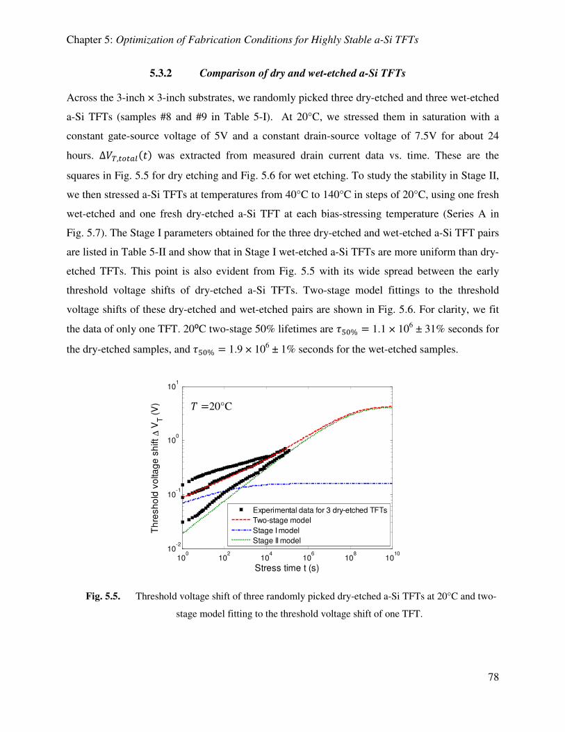
Chapter 5: Optimization of Fabrication Conditions for Highly Stable a-Si TFTs
78
5.3.2 Comparison of dry and wet-etched a-Si TFTs
Across the 3-inch × 3-inch substrates, we randomly picked three dry-etched and three wet-etched
a-Si TFTs (samples #8 and #9 in Table 5-I). At 20°C, we stressed them in saturation with a
constant gate-source voltage of 5V and a constant drain-source voltage of 7.5V for about 24
hours. ∆��,���� � was extracted from measured drain current data vs. time. These are the
squares in Fig. 5.5 for dry etching and Fig. 5.6 for wet etching. To study the stability in Stage II,
we then stressed a-Si TFTs at temperatures from 40°C to 140°C in steps of 20°C, using one fresh
wet-etched and one fresh dry-etched a-Si TFT at each bias-stressing temperature (Series A in
Fig. 5.7). The Stage I parameters obtained for the three dry-etched and wet-etched a-Si TFT pairs
are listed in Table 5-II and show that in Stage I wet-etched a-Si TFTs are more uniform than dry-
etched TFTs. This point is also evident from Fig. 5.5 with its wide spread between the early
threshold voltage shifts of dry-etched a-Si TFTs. Two-stage model fittings to the threshold
voltage shifts of these dry-etched and wet-etched pairs are shown in Fig. 5.6. For clarity, we fit
the data of only one TFT. 20⁰C two-stage 50% lifetimes are �/%% = 1.1 × 10⁶ ± 31% seconds for
the dry-etched samples, and �/%% = 1.9 × 10⁶ ± 1% seconds for the wet-etched samples.
Fig. 5.5. Threshold voltage shift of three randomly picked dry-etched a-Si TFTs at 20°C and two-
stage model fitting to the threshold voltage shift of one TFT.
100
102
104
106
108
1010
10-2
10-1
100
101
Stress time t (s)
Th
resh
old
vo
ltag
e s
hift ∆
VT (
V)
Experimental data for 3 dry-etched TFTs
Two-stage model
Stage I model
Stage II model
- =20°C

Chapter 5: Optimization of Fabrication Conditions for Highly Stable a-Si TFTs
79
Fig. 5.6. Threshold voltage shift of three randomly picked wet-etched a-Si TFTs at 20°C and two-
stage model fitting to the threshold voltage shift of one TFT.
Table 5-II. Stage I fitting parameters for dry and wet-etched a-Si TFTs
Dry-etched a-Si TFTs Wet-etched a-Si TFTs
Sample ∆����,�
(V) %,� (s) .�
∆����,� (V)
%,� (s) .�
1 0 0 NA 0.24 35 0.24
2 0.16 28.8 0.18 0.23 15 0.25
3 0.25 1.4 0.36 0.23 39 0.24
Average 0.14±93% 10.1±160% 0.27±48
% 0.23±2.5% 30±43% 0.24±2.3%
We studied the stability of the dry-etched and wet-etched TFTs in Stage II by bias-stressing at
elevated temperatures. The fitting parameters for Series A in Fig. 5.7 obtained from the Stage II
model (5. 3) are listed in Table 5-III. The times when the drain current has dropped to its initial
value (50% lifetimes �/%%) are shown in the Arrhenius plot for Series A in Fig. 5.7. The squares
are the experimentally measured 50% lifetimes at high temperatures, and the straight lines are
50% lifetime �/%%,�� extracted from the Stage II model fits (5. 3), which enables us to extrapolate
100
102
104
106
108
1010
10-2
10-1
100
101
Stress time t (s)
Th
resh
old
vo
ltag
e s
hift
∆ V
T (
V)
Experimental data for 3 wet-etched TFTs
Two-stage model
Stage I model
Stage II model
- =20°C

Chapter 5: Optimization of Fabrication Conditions for Highly Stable a-Si TFTs
80
from the elevated bias-stress temperatures to room temperature. It can be seen that the wet-
etched a-Si TFTs have a better long-term stability. The Stage II model produces this result
because the wet-etched a-Si TFTs have a lower -% than dry-etched a-Si TFTs, while the
parameters & and )*� are similar (see Table 5-III). A lower -% means that the energy
distribution of weak Si-Si bonds in wet-etched a-Si TFTs is steeper than that in dry-etched TFTs.
To confirm this conclusion about dry-etching and wet-etching effects on Stage II stability, we
measured another series of dry and wet-etched a-Si TFTs (Series B in Fig. 5.7) fabricated under
different deposition conditions (#5 and #6 in Table 5-I). Again, wet-etched a-Si TFTs have a
better stability in Stage II.
Fig. 5.7. Stage II 50% lifetime at different temperatures for two series of dry and wet-etched a-Si
TFTs (solid squares: experimental data; straight lines: stage II model).
Table 5-III. Stage II fitting parameters for dry and wet-etched a-Si TFTs
ν (Hz) 34 (K) 5678 (eV)
Dry-etched a-Si
TFTs 5 × 10
5 964 0.78
Wet-etched a-Si
TFTs 5 × 10
5 793 0.78
2.2 2.4 2.6 2.8 3.0 3.2 3.4 3.610
2
103
104
105
106
107
108
Reciprocal Temperature 1000/T (K-1)
50
% li
fetim
e τ
50%
,II (
s)
140 120 100 80 60 40 20
Wet-etched
Dry-etched
Series A
(#8 and #9)
Series B
(#5 and #6)

Chapter 5: Optimization of Fabrication Conditions for Highly Stable a-Si TFTs
81
5.3.3 Discussion
Three sources in a reactive ion etching (RIE) that can cause damage TFTs [14]: ion
bombardment, plasma radiation and surface charge buildup. Ion bombardment causes the surface
damage. Because our a-Si TFTs have the back-channel passivated structure, surface damage
from ion bombardment should not affect the channel region. In Fig. 5.5, we observed that dry-
etching induced widely distributed threshold voltage shifts in Stage I. As discussed in Chapter 4,
the instability in Stage I is most likely caused by the charge trapping in the gate SiNx. Therefore,
we attribute the non-uniform threshold voltage shifts of the dry-etched a-Si TFTs in Stage I to
spatially non-uniform surface charge buildup during plasma etching, which can induce surface
states at the SiNx / a-Si interface and eventually trap charge in SiNx [15]. The long-term
instability of Stage II is caused by defect creation in a-Si. The deterioration of long-term stability
in Stage II (Fig. 5.7) caused by RIE probably is the result of the high photon energy plasma
radiation, which could cause the Staebler-Wronski type defects in the a-Si layer that are not fully
reversible by thermal annealing [14, 16]. Comparing the stability between dry and wet-etched a-
Si TFTs suggests that some damage caused by RIE remains after a one-hour long annealing at
180°C [8].
5.4. Summary and conclusion
Using results from low gate-field stress over a range of temperatures, and their fit to a two-stage
model for threshold voltage shift, we evaluated the effect of a-Si TFT fabrication steps on the
stability of the drain current. The main measure of stability is the time over which the drain
current drops to 50% of its initial value. That time is either measured, or extrapolated from
shorter-time measurements using the two-stage model. The stability of a-Si TFTs are determined
by deposition conditions and etching methods, which are summarized in Table 5-I. The
instability in Stage I leads to a maximum threshold voltage shift ∆����,( ≤ 0.3 V. As a result,
the two-stage 50% lifetime is mainly determined by Stage II. Instability in Stage II is caused by
defect creation in a-Si and can be characterized by three parameters the attempt-to-escape
frequency &, activation energy )*� and characteristic temperature -% in (5. 4) and (5. 5). The
statistical dependence of two-stage 50% lifetimes on these three parameters for a-Si TFTs in
Table 5-I are illustrated in Fig. 5.8, Fig. 5.9 and Fig. 5.10. The a-Si TFTs with large &, high )*� and low -% have better stability and long lifetime. As pointed out in Chapter 4, a-Si with high

Chapter 5: Optimization of Fabrication Conditions for Highly Stable a-Si TFTs
82
)*� and low -% has high barrier energies for defect creation and small disorder in structure. Note
that the attempt-to-escape frequency & is the effective attempt-to-escape frequency [17], which
measures combined effect of both defect creation and defect annealing. Thus, a-Si TFTs with
large & do not necessarily tend to be unstable. In contrast, as shown in Fig. 5.8, the most stable a-
Si TFTs have a large &.
Fig. 5.8. Dependence of two-stage 50% lifetimes on the attempt-to-escape frequency &.
Fig. 5.9. Dependence of two-stage 50% lifetimes on the activation energy )*�.
103
104
105
106
107
103
104
105
106
107
108
ν (Hz)
Tw
o-s
tag
e 5
0%
life
time
(s)
0.5 0.6 0.7 0.8 0.9 110
3
104
105
106
107
108
109
Eact
(eV)
Tw
o-s
tag
e 5
0%
life
time
(s)

Chapter 5: Optimization of Fabrication Conditions for Highly Stable a-Si TFTs
83
Fig. 5.10. Dependence of two-stage 50% lifetimes on the characteristic temperature -%
Another important result is that reaching high stability requires the coupling of several
parameters for processing the SiNx gate insulator and the a-Si channel layer. The optimum NH3 /
SiH4 gas flow ratio is 10, and hydrogen dilution makes the SiNx more stable. The most stable a-
Si is deposited at high temperature, but not exceeding the temperature of SiNx deposition. An H2
/ SiH4 flow ratio of 5 produces the most stable a-Si. One important result is that reaching high
stability requires the coupling of several parameters for processing the SiNx gate insulator and
the a-Si channel layer. When the SiNx gate dielectric is deposited with H2 dilution, the a-Si
deposited on top of it becomes more stable than when the gate SiNx is deposited without H2
dilution. We also find that the highest TFT stability is achieved when both the SiNx and a-Si
layers near the SiNx /a-Si interface are grown at low plasma power. By combining these
deposition techniques we raised the extrapolated 50% lifetime of the drain current under
continuous operation from 3.3 × 10⁴ sec (9.2 hours) to 4.4 × 10
7 sec (1.4 years). Etching is the
most important post-deposition process that affects stability. We developed a TFT fabrication
process with four wet etch steps, which produces TFTs that are more uniform in Stage I and
more stable in Stage II than those processed with plasma etching.
600 700 800 900 1000 1100 120010
4
105
106
107
108
T0 (K)
Tw
o-s
tag
e 5
0%
life
time
(s)

Chapter 5: Optimization of Fabrication Conditions for Highly Stable a-Si TFTs
84
References:
[1] B. Hekmatshoar, S. Wagner, and J. C. Sturm, "Tradeoff regimes of lifetime in amorphous
silicon thin-film transistors and a universal lifetime comparison framework," Applied
Physics Letters, vol. 95, Oct 5 2009.
[2] B. Dunnett, C. H. Cooper, D. T. Murley, R. A. G. Gibson, D. I. Jones, M. J. Powell, S. C.
Deane, and I. D. French, "Equilibration in Amorphous Silicon Nitride Alloys," Materials
Reseach Society Symposium Proceedings, vol. 377, pp. 349-354, 1995.
[3] I. D. French, C. J. Curling, and A. L. Goodyear, "Silicon Nitride Optimisation for A-Si:H
Tfts Used in Projection LC-TVS," Materials Reseach Society Symposium Proceedings,
vol. 336, pp. 769-774, 1994.
[4] I. D. French, S. C. Deane, D. T. Murley, J. Hewett, I. G. Gale, and M. J. Powell, "The
Effect of the Amorphous Silicon Alpha-Gamma Transition on Thin Film Transistor
Performance," Materials Reseach Society Symposium Proceedings, vol. 467, pp. 875-
880, 1997.
[5] R. B. Wehrspohn, S. C. Deane, I. D. French, J. Hewett, and M. J. Powell, "Stability of
Amorphous Silicon Thin Film Transistors," Materials Reseach Society Symposium
Proceedings, vol. 557, pp. 365-370, 1999.
[6] B. Hekmatshoar, K. H. Cherenack, S. Wagner, and J. C. Sturm, "Amorphous silicon thin-
film transistors with DC saturation current half-life of more than 100 years," in Electron
Devices Meeting, 2008. IEDM 2008. IEEE International, 2008, pp. 1-4.
[7] B. Hekmatshoar, K. H. Cherenack, A. Z. Kattamis, K. Long, S. Wagner, and J. C. Sturm,
"Highly stable amorphous-silicon thin-film transistors on clear plastic," Applied Physics
Letters, vol. 93, Jul 21 2008.
[8] S. M. GadelRab, A. M. Miri, and S. G. Chamberlain, "A comparison of the performance
and reliability of wet-etched and dry-etched alpha-Si : H TFT's," Ieee Transactions on
Electron Devices, vol. 45, pp. 560-563, Feb 1998.
[9] D. Murley, I. French, S. Deane, and R. Gibson, "The effect of hydrogen dilution on the
aminosilane plasma regime used to deposit nitrogen-rich amorphous silicon nitride,"
Journal of Non-Crystalline Solids, vol. 198, pp. 1058-1062, May 1996.
[10] D. L. Smith, A. S. Alimonda, C. C. Chen, S. E. Ready, and B. Wacker, "Mechanism of
Sinxhy Deposition from Nh3-Sih4 Plasma," Journal of the Electrochemical Society, vol.
137, pp. 614-623, Feb 1990.
[11] K. Hiranaka, T. Yoshimura, and T. Yamaguchi, "Influence of an a-SiNx:H gate insulator
on an amorphous silicon thin-film transistor," Journal of Applied Physics, vol. 62, pp.
2129-2135, 1987.
[12] B. Hekmatshoar, "Highly stable amorphous silicon thin film transistors and integration
approaches for reliable organic light emitting diode displays on clear plastic," Thesis (Ph
D), Princeton University, 2010.
[13] T. Yoshimura, K. Hiranaka, T. Yamaguchi, S. Yanagisawa, and K. Asama,
"Characterization of a-Si:H Near a-Sinx:H/a-Si:H Interface by Photoluminescence
Spectra," Materials Reseach Society Symposium Proceedings, vol. 70, pp. 373-378, 1986.
[14] Y. Kuo, "Reactive Ion Etch Damages in Inverted, Trilayer Thin-Film Transistor,"
Applied Physics Letters, vol. 61, pp. 2790-2792, Dec 7 1992.

Chapter 5: Optimization of Fabrication Conditions for Highly Stable a-Si TFTs
85
[15] S. C. Fang and J. P. Mcvittie, "A Model and Experiments for Thin Oxide Damage from
Wafer Charging in Magnetron Plasmas," Ieee Electron Device Letters, vol. 13, pp. 347-
349, Jun 1992.
[16] D. L. Staebler and C. R. Wronski, "Reversible Conductivity Changes in Discharge-
Produced Amorphous Si," Applied Physics Letters, vol. 31, pp. 292-294, 1977.
[17] H. Fritzsche, Amorphous silicon and related materials. Singapore ; Teaneck, N.J.: World
Scientific, 1989.

Chapter 6: Redistribution of Gap State Density after Low Gate-Field Stress
86
Redistribution of Gap State Density after Low Gate-Field Stress
In Chapter 4, two stages of the threshold voltage shift were identified and modeled with the two-
stage model. The threshold voltage shifts in the two stages were both modeled with the stretched
exponential expression. Stage I initially dominates up to hours or days near room temperature
and is attributed to charge trapping in the gate SiNx. Stage II dominates in the long term and is
attributed to defect creation in a-Si. Although most reports suggest that defect creation is the
dominant mechanism for the threshold voltage shift under low gate-field as assumed in Chapter 4
[1-6], a consensus has yet to be reached [7].
In this Chapter, the gap state density in a-Si is determined from the analysis of the field-effect
characteristics [8, 9] in the a-Si TFT before and after low-gate field stress. Although this
technique to measure the density of states (DOS) has limitations, such as in distinguishing
between bulk and interface states [10], it provides adequate information to show that the gap
state density is redistributed after a constant low gate field stress [11]. The redistribution of gap
state density suggests that the low gate-field leads to increased mid gap states and decreased tail
states. This provides evidence to show that defect creation occurs in a-Si TFTs under low-gate
field.
6.1. Theory of field-effect technique to determine gap state density
We consider a metal/insulator/amorphous silicon (MIS) structure as illustrated in Fig. 6.1. With
several assumptions and approximations in Section 6.1.1, the gap state density can be obtained
from the surface potential, which can be determined from the field-induced conductance.
6.1.1 Assumptions and approximations
To develop the field-effect technique, assumptions and approximations are made to simplify the
procedure to obtain the relationship between gap state density and field-effect conductance.
Chapter 6

Chapter 6: Redistribution of Gap State Density after Low Gate-Field Stress
87
Fig. 6.1. Energy band diagram of the metal / insulator / amorphous silicon (MIS) structure with a
positive gate bias and schematic density of states distribution.
− Spatially uniform distribution of gap states [10]
We assume that the distribution of gap states ���� is uniform in the a-Si from the surface region
near the gate insulator into the a-Si bulk region. It is natural to make this assumption for fresh a-
Si TFTs with uniformly deposited a-Si. However, for a-Si TFTs after low-field stress,���� in
the surface region is different from that in the bulk region, because the heavier free-carrier
concentration in the surface region induces more defects there. The validity of this assumption
will be discussed in Section 6.4.
− Zero-temperature statistics [9, 10]
For sufficiently low temperatures, it can be assumed that all induced charges are in localized
states, thus neglecting the space charge of the free carriers.
− Unmodulated bulk [10]
For a-Si TFTs with a ~200 nm thick a-Si layer, it makes sense to assume that the bulk region far
away from the a-Si / insulator interface is unmodulated, i.e.
������
= 0 (6. 1)

Chapter 6: Redistribution of Gap State Density after Low Gate-Field Stress
88
where �� is the thickness of the a-Si layer, and � = 0 is the position at the a-Si / insulator
interface (Fig. 6.1).
− Negligible effect of the interface states [10]
For our good quality a-Si TFTs with interface state density below 1011
cm-2
eV-1
, the effect of
interface states can be neglected without leading to serious errors [12].
6.1.2 Determination of gap state density
We represent the field-effect technique as described in Ref. 14 and Ref. 15. The band bending in
the a-Si layer, ���� (Fig. 6.1), follows Poisson’s equation:
������� = − ���
��� (6. 2)
where ��� is the a-Si dielectric constant and ���� is the local space-charge density at � due to the
local Fermi-level shift of �����. With the assumption of zero-temperature statistics, ���� is
related to the gap state density distribution ���� by
���� = −� � ������� !"#���� ! (6. 3)
After multiplying by 2�����/�� and integrating from the insulator / a-Si interface at � = 0 to
the unmodulated neutral bulk at � = ��, we obtain
&������'(= (#
���� ��� � ������� !"#�
� !��� (6. 4)
where �� is the band bending at � = 0. Then, the gap state density is expressed by
���)* + ���� = ���(#
,�,���
&������'( (6. 5)
Assuming negligible interface states, the electric field at the insulator / a-Si interface is given by
������ = −
��-����
.�-���-�
= − ��-����
./0. 10����-�
(6. 6)
where ��2� is the gate insulator dielectric constant and ��2� is the thickness of the insulator layer,
3)4 is the flat band voltage, 35 is the gate voltage, and 3�2� is the voltage drop across the
Chapter 6: Redistribution of Gap State Density after Low Gate-Field Stress
89
insulator. Combining (6. 5) and (6. 6), the density of the gap states can be calculated, if the
relation between 35 and �� is known.
6.1.3 Relation between gate voltage and surface potential [9]
The surface potential �� can be determined from the measured field-induced conductance as a
function of gate voltage. The sheet conductance 6 is written as
6 = 6)4 + 6)4 7�� 8exp<�����/=>? − 1A����
= 6)4 − 6)4 7#�
� BCD�#�/EF�07��/� �����#�����
� (6. 7)
where 6)4 refers to the conductance for the flat band condition, i.e. �� = 0. The increment in the
gate voltage G35 causes a corresponding change in the surface potential G��. As a consequence,
the sheet conductance modulation G6 is given by
G6 = −6)4 7#�
BCD�#��/EF�07���/�|IJ�
G����� (6. 8)
From this and (6. 6), we have
G�� = KLL 1
��-����
���-�
./0. 10��<BCD�#�� EF⁄ �07? (6. 9)
Starting from 35 = 3)4, the surface potential �� as a function of gate voltage 35 can be
successively obtained using (6. 9).
6.1.4 Sheet conductance calculation
Because the a-Si active layer is intrinsic and a high field exists everywhere in the a-Si TFT, the
current is a drift current in both the subthreshold region and above threshold region [13]. Thus,
the field-induced sheet conductanceσ is the inverse of sheet resistance and can be calculated
from the TFT transfer characteristics of drain current OP vs. gate voltage 35 for very low drain
bias with
6�35� = 7Q�= 7
.R/SR�./�∙U/V= SR�./�V
.RU (6. 10)
Thus, sheet conductance as a function of gate voltage 35 can be obtained.

Chapter 6: Redistribution of Gap State Density after Low Gate-Field Stress
90
Substituting (6. 10) into (6. 9) enables us to obtain the relation between the surface potential �� and the gate voltage 35. Then with (6. 5) and (6. 6), the gap state density can be determined.
6.2. Sample preparation and measurement
The sample was fabricated with the dry-etching process described in Chapter 3. 300-nm gate
nitride, 200-nm intrinsic hydrogenated a-Si and 300-nm passivation nitride were deposited
sequentially at 320°C, 220°C and 220°C, respectively. At the end of the process, the sample was
annealed at 180°C for an hour. After annealing, a gate-bias voltage sweep at a fixed drain voltage
0.1 V was applied to measure the OP - 35 transfer characteristics of a fresh a-Si TFT at room
temperature. Then the a-Si TFT was biased with a constant gate voltage 35 = 5 V (a low-gate
field of ~1.5 × 10⁵
V/cm) at 120⁰C for 5 minutes. The high temperature stress at 120⁰C was used
to accelerate the threshold voltage shift under low-gate field stress. The drain voltage was set at
zero, so the threshold voltage shift along the channel was uniform. After the 5-miniute bias-
temperature stress, another gate-bias voltage sweep at a fixed drain voltage 0.1 V was applied to
measure the OP - 35 transfer characteristics at room temperature. During the two OP - 35 sweeps,
a small drain voltage 3P = 0.1 V (<<35 = 5 V to make the channel generally uniform) was
applied to obtain the field-effect conductance.
6.3. Experiment results and gap state density determination
The a-Si TFT we measured has a channel width of W = 150 µm and a channel length of X = 15
µm. OP - 35 transfer characteristics before and after the low-gate field stress are shown in Fig.
6.2. Before stress, the threshold voltage was 3F� = 1.54 V, the field-effect mobility was Y)�F� =
0.83 cm2/V·s, and the subthreshold slope was ZZ� = 235 mV/dec. After stress, the threshold
voltage was 3F = 2.38 V, the field-effect mobility was Y)�F = 0.83 cm2/V·s, and the
subthreshold slope was ZZ = 240 mV/dec. After the gate-bias stress at 120⁰C, the threshold
voltage shifts, the subthreshold slope slightly increases (Fig. 6.2(a)) and the field-effect mobility
stays almost unchanged (Fig. 6.2(b)).