Embed Size (px)
Citation preview

PUBLIC
94-00-00-01 - 1 - Cobham Semiconductor Solutions Version 1.2.3 www.cobham.com/HiRel
Standard Product
UT699E/UT700 LEON 3FT SPARCTM V8 Microprocessor Functional Manual Cobham.com/HiRel September 12, 2018 The most important thing we build is trust

PUBLIC
94-00-00-01 - 2 - Cobham Semiconductor Solutions Version 1.2.3 www.cobham.com/HiRel
Table of Contents
Introduction ...................................................................................... 13 Chapter 1:
1.1 Scope ........................................................................................................ 13
1.2 Differences between UT699, UT699E, and UT700 ......................................... 13
1.3 Architecture ................................................................................................ 15
1.4 Memory Map .............................................................................................. 16
1.5 Interrupts ................................................................................................... 17
1.6 Signals ....................................................................................................... 17
1.7 Clocking ..................................................................................................... 20
Clock Inputs ......................................................................................... 20 1.7.1
Clock Output ........................................................................................ 20 1.7.2
LEON 3FT SPARC V8 32-bit Microprocessor ......................................... 21 Chapter 2:
2.1 Overview .................................................................................................... 21
Integer Unit ......................................................................................... 21 2.1.1
Cache Sub-System ................................................................................ 21 2.1.2
Floating-Point Unit ................................................................................ 22 2.1.3
Memory Management Unit .................................................................... 22 2.1.4
On-Chip Debug Support ........................................................................ 22 2.1.5
Interrupt Port ....................................................................................... 22 2.1.6
AMBA Interface .................................................................................... 22 2.1.7
Power-Down Mode ............................................................................... 22 2.1.8
2.2 LEON 3FT Integer Unit ................................................................................ 22
Overview .............................................................................................. 22 2.2.1
Instruction Pipeline ............................................................................... 23 2.2.2
SPARC Implementer’s ID ....................................................................... 25 2.2.3
Division Instructions ............................................................................. 25 2.2.4
Multiplication Instructions...................................................................... 25 2.2.5
Branch Prediction ................................................................................. 25 2.2.6
Hardware Breakpoints ........................................................................... 25 2.2.7
Instruction Trace Buffer ........................................................................ 27 2.2.8
Processor Configuration Register ........................................................... 27 2.2.9
Exceptions ........................................................................................ 28 2.2.10
Single Vector Interrupt (SVT) ............................................................. 29 2.2.11
PUBLIC
94-00-00-01 - 3 - Cobham Semiconductor Solutions Version 1.2.3 www.cobham.com/HiRel
Address Space Identifiers (ASI) .......................................................... 29 2.2.12
Power-Down ..................................................................................... 30 2.2.13
Processor Reset Operation ................................................................. 30 2.2.14
Integer Unit SEU Protection ................................................................ 30 2.2.15
2.3 Floating Point Unit ...................................................................................... 30
Floating Point Unit Functional Description ............................................... 31 2.3.1
Floating Point Number Formats ............................................................. 31 2.3.2
Floating Point Operations ...................................................................... 31 2.3.3
Exceptions ........................................................................................... 33 2.3.4
Rounding ............................................................................................. 33 2.3.5
Denormalized numbers ......................................................................... 33 2.3.6
Non-standard Mode .............................................................................. 33 2.3.7
Not-A-Number (NaN) ............................................................................ 33 2.3.8
2.4 Floating Point Unit ...................................................................................... 34
Overview .............................................................................................. 34 2.4.1
Instruction Cache ................................................................................. 34 2.4.2
Data Cache .......................................................................................... 35 2.4.3
Write Buffer ......................................................................................... 35 2.4.4
Instruction and Data Cache Tags ........................................................... 35 2.4.5
Cache Flushing ..................................................................................... 37 2.4.6
Data Cache Snooping ............................................................................ 37 2.4.7
Diagnostic Cache Access ....................................................................... 37 2.4.8
Cache Control Register .......................................................................... 38 2.4.9
Error Protection ................................................................................. 40 2.4.10
Cache Configuration Registers ............................................................ 41 2.4.11
Software Consideration ...................................................................... 42 2.4.12
2.5 Memory Management Unit .......................................................................... 42
MMU ASI Usage .................................................................................... 42 2.5.1
Cache Operation ................................................................................... 43 2.5.2
MMU Registers ..................................................................................... 43 2.5.3
Translation Look-Aside Buffer (TLB) ....................................................... 46 2.5.4
2.6 LEON 3FT Storage Allocation ....................................................................... 46
Integer Unit Register File ...................................................................... 46 2.6.1

PUBLIC
94-00-00-01 - 4 - Cobham Semiconductor Solutions Version 1.2.3 www.cobham.com/HiRel
Floating Point Unit (FPU) Register File .................................................... 47 2.6.2
Cache Memories ................................................................................... 47 2.6.3
Memory Controller with EDAC ............................................................. 49 Chapter 3:
3.1 Overview .................................................................................................... 49
3.2 PROM Access .............................................................................................. 49
3.3 Memory Mapped I/O ................................................................................... 50
3.4 SRAM Access .............................................................................................. 50
3.5 8-bit and 16-bit PROM and SRAM Access ...................................................... 50
3.6 8-bit and 16-bit I/O Accesses ...................................................................... 52
3.7 Burst Cycles ............................................................................................... 52
3.8 SDRAM Access ............................................................................................ 52
General ................................................................................................ 53 3.8.1
Address Mapping .................................................................................. 53 3.8.2
Initialization ......................................................................................... 53 3.8.3
Configurable SDRAM Timing Parameters ................................................ 53 3.8.4
3.9 Refresh ...................................................................................................... 54
SDRAM Commands ............................................................................... 54 3.9.1
Read Cycles.......................................................................................... 54 3.9.2
Write Cycles ......................................................................................... 54 3.9.3
Address Bus ......................................................................................... 54 3.9.4
Data Bus .............................................................................................. 54 3.9.5
Clocking ............................................................................................... 54 3.9.6
Initialization ......................................................................................... 55 3.9.7
3.10 Memory EDAC ......................................................................................... 55
BCH EDAC ......................................................................................... 55 3.10.1
Reed-Solomon EDAC .......................................................................... 55 3.10.2
EDAC Error Reporting ........................................................................ 57 3.10.3
3.11 Using 𝐁𝐑𝐃𝐘 ............................................................................................ 57
3.12 Access Errors ........................................................................................... 57
3.13 Attaching an External DRAM Controller...................................................... 57
3.14 Registers ................................................................................................. 58
Memory Configuration Register 1 (MCFG1) .......................................... 58 3.14.1
Memory Configuration Register 2 (MCFG2) .......................................... 59 3.14.2

PUBLIC
94-00-00-01 - 5 - Cobham Semiconductor Solutions Version 1.2.3 www.cobham.com/HiRel
Memory Configuration Register 3 (MCFG3) .......................................... 61 3.14.3
Memory Configuration Register 4 (MCFG4) .......................................... 62 3.14.4
3.15 Boot Strap Configuration .......................................................................... 63
3.16 PROM, SRAM, and Memory Mapped I/O Timing Diagrams .......................... 63
3.17 SDRAM Timing Diagram ........................................................................... 70
AHB Status Registers ......................................................................... 71 Chapter 4:
4.1 Overview .................................................................................................... 71
4.2 Operation ................................................................................................... 71
4.3 Correctable Errors ....................................................................................... 71
4.4 Interrupts ................................................................................................... 71
4.5 Registers .................................................................................................... 71
Interrupt Controller ............................................................................ 73 Chapter 5:
5.1 Overview .................................................................................................... 73
Interrupt Prioritization ........................................................................... 73 5.1.1
Interrupt Allocation ............................................................................... 74 5.1.2
5.2 Registers .................................................................................................... 74
Interrupt Level Register ........................................................................ 74 5.2.1
Interrupt Pending Register .................................................................... 75 5.2.2
Interrupt Force Register ........................................................................ 75 5.2.3
Interrupt Clear Register ........................................................................ 76 5.2.4
Interrupt Status Register ....................................................................... 76 5.2.5
Interrupt Mask Register ........................................................................ 77 5.2.6
Extended Interrupt Acknowledge Register .............................................. 77 5.2.7
UART with APB Interface ................................................................... 79 Chapter 6:
6.1 Overview .................................................................................................... 79
6.2 Operation ................................................................................................... 79
Transmitter Operation ........................................................................... 79 6.2.1
Receiver Operation ............................................................................... 80 6.2.2
6.3 Baud Rate Generation ................................................................................. 80
Loop Back Mode ................................................................................... 81 6.3.1
Interrupt Generation ............................................................................. 81 6.3.2
6.4 UART Registers ........................................................................................... 81
UART Data Register .............................................................................. 81 6.4.1

PUBLIC
94-00-00-01 - 6 - Cobham Semiconductor Solutions Version 1.2.3 www.cobham.com/HiRel
UART Status Register ............................................................................ 82 6.4.2
UART Control Register .......................................................................... 83 6.4.3
UART Scaler Register ............................................................................ 84 6.4.4
Timer Unit ......................................................................................... 86 Chapter 7:
7.1 Overview .................................................................................................... 86
7.2 Operation ................................................................................................... 86
7.3 Registers .................................................................................................... 87
General Purpose I/O Port ................................................................... 91 Chapter 8:
8.1 Overview .................................................................................................... 91
8.2 Operation ................................................................................................... 91
8.3 Register ..................................................................................................... 91
GPIO Port Input Value Register ............................................................. 92 8.3.1
GPIO Port Data Output Register ............................................................ 92 8.3.2
GPIO Port Data Direction Register ......................................................... 93 8.3.3
GPIO Interrupt Mask Register ................................................................ 93 8.3.4
GPIO Interrupt Priority Register ............................................................. 94 8.3.5
GPIO Interrupt Edge Register ................................................................ 94 8.3.6
PCI Master/Target Unit ...................................................................... 96 Chapter 9:
9.1 Overview .................................................................................................... 96
9.2 Operation ................................................................................................... 96
PCI Target Unit .................................................................................... 96 9.2.1
PCI Master Unit .................................................................................... 96 9.2.2
Burst Transactions ................................................................................ 97 9.2.3
Byte Twisting ....................................................................................... 97 9.2.4
9.3 PCI Target Interface ................................................................................... 97
9.4 PCI Target Configuration Space Header Registers ......................................... 98
9.5 PCI Target Map Registers .......................................................................... 103
PAGE0 Register .................................................................................. 103 9.5.1
PAGE1 Register .................................................................................. 104 9.5.2
9.6 PCI Master Interface ................................................................................. 105
PCI Configuration Cycles ..................................................................... 105 9.6.1
PCI I/O Cycles .................................................................................... 106 9.6.2
PCI Memory Cycles ............................................................................. 106 9.6.3

PUBLIC
94-00-00-01 - 7 - Cobham Semiconductor Solutions Version 1.2.3 www.cobham.com/HiRel
9.7 PCI Host Operation ................................................................................... 107
9.8 Interrupt Support...................................................................................... 107
9.9 Registers .................................................................................................. 107
DMA Controller for the GRPCI Interface ............................................ 115 Chapter 10:
10.1 Introduction .......................................................................................... 115
10.2 Operation .............................................................................................. 115
10.3 Registers ............................................................................................... 116
PCI Arbiter, PCIARB ......................................................................... 119 Chapter 11:
11.1 Overview ............................................................................................... 119
11.2 Operation .............................................................................................. 119
Scheduling Algorithm ....................................................................... 119 11.2.1
Timeout .......................................................................................... 119 11.2.2
Turn-Around ................................................................................... 119 11.2.3
Bus Parking ..................................................................................... 120 11.2.4
Lock ............................................................................................... 120 11.2.5
Latency ........................................................................................... 120 11.2.6
SpaceWire Interface with RMAP support (GRSPW2) ........................... 121 Chapter 12:
12.1 Overview ............................................................................................... 121
12.2 Operation .............................................................................................. 121
Overview ........................................................................................ 121 12.2.1
Protocol Support .............................................................................. 122 12.2.2
12.3 Link Interface ........................................................................................ 122
Link Interface FSM ........................................................................... 122 12.3.1
Transmitter ..................................................................................... 123 12.3.2
Receiver .......................................................................................... 124 12.3.3
Time Interface ................................................................................. 125 12.3.4
12.4 Receiver DMA Channels ......................................................................... 125
Address Comparison and Channel Selection....................................... 125 12.4.1
Basic Link Functionally of a Channel .................................................. 127 12.4.2
Setting up the GRSPW2 for Reception ............................................... 128 12.4.3
Setting up the Descriptor ................................................................. 128 12.4.4
Enabling Descriptors ........................................................................ 128 12.4.5
Setting up the DMA Control Register ................................................. 130 12.4.6

PUBLIC
94-00-00-01 - 8 - Cobham Semiconductor Solutions Version 1.2.3 www.cobham.com/HiRel
The Effect to the Control Bits during Reception ................................. 130 12.4.7
Status Bits ....................................................................................... 131 12.4.8
Error Handling ................................................................................. 131 12.4.9
Promiscuous Mode ........................................................................... 132 12.4.10
12.5 Transmitter DMA Channels ..................................................................... 132
Basic Functionality of a Channel ....................................................... 132 12.5.1
Setting up the GRSPW2 for Transmission .......................................... 132 12.5.2
Enable Descriptors ........................................................................... 132 12.5.3
Starting Transmission ...................................................................... 133 12.5.4
The Transmission Process ................................................................ 136 12.5.5
The Descriptor Register.................................................................... 136 12.5.6
Error Handling ................................................................................. 136 12.5.7
12.6 Remote Memory Access Protocol (RMAP) ................................................ 137
Fundamentals of the Protocol ........................................................... 137 12.6.1
Implementation ............................................................................... 137 12.6.2
Write Commands ............................................................................. 139 12.6.3
Read Commands ............................................................................. 139 12.6.4
Read-Modify-Write Commands ......................................................... 139 12.6.5
Controls .......................................................................................... 139 12.6.6
12.7 AMBA Interface ..................................................................................... 142
APB Slave Interface ......................................................................... 143 12.7.1
AHB Master Interface ....................................................................... 143 12.7.2
12.8 SpaceWire Clock Generation ................................................................... 143
12.9 Register ................................................................................................ 143
CAN 2.0 Interface ............................................................................ 155 Chapter 13:
13.1 Overview ............................................................................................... 155
13.2 AHB Interface ........................................................................................ 155
13.3 BasicCAN Mode...................................................................................... 156
BasicCAN Register Map (Address 0xFFF20000 and 0xFFF20100) ......... 156 13.3.1
Control Register............................................................................... 157 13.3.2
Command Register .......................................................................... 157 13.3.3
Status Register ................................................................................ 157 13.3.4
Interrupt Register ............................................................................ 158 13.3.5

PUBLIC
94-00-00-01 - 9 - Cobham Semiconductor Solutions Version 1.2.3 www.cobham.com/HiRel
Transmit Buffer ............................................................................... 159 13.3.6
Receive Buffer ................................................................................. 159 13.3.7
Acceptance Filter ............................................................................. 159 13.3.8
13.4 PeliCAN Mode ........................................................................................ 159
PeliCAN Register Map (Address 0xFFF20000 and 0xFFF20100) ........... 159 13.4.1
Mode Register ................................................................................. 160 13.4.2
Command Register .......................................................................... 161 13.4.3
Status Register ................................................................................ 161 13.4.4
Interrupt Register ............................................................................ 162 13.4.5
Interrupt Enable Register ................................................................. 163 13.4.6
Arbitration Lost Capture Register ...................................................... 163 13.4.7
Error Code Capture Register ............................................................. 163 13.4.8
Error Warning Limit Register ............................................................ 164 13.4.9
RX Error Counter Register, Offset 14 ................................................. 165 13.4.10
TX Error Counter Register, Offset 15 ................................................. 165 13.4.11
Transmit Buffer ............................................................................... 165 13.4.12
Receiver Buffer ................................................................................ 167 13.4.13
Acceptance Filter ............................................................................. 169 13.4.14
RX Message Counter ........................................................................ 170 13.4.15
13.5 Common Registers ................................................................................. 170
Clock Divider Register ...................................................................... 170 13.5.1
Bus Timing 0 ................................................................................... 171 13.5.2
Bus Timing 1 ................................................................................... 171 13.5.3
13.6 CAN-OC vs SJA1000 ............................................................................... 171
Ethernet Media Access Controller (MAC) with EDCL Support ............... 173 Chapter 14:
14.1 Overview ............................................................................................... 173
14.2 Operation .............................................................................................. 173
System Overview ............................................................................. 173 14.2.1
Protocol Support .............................................................................. 174 14.2.2
Hardware Requirements ................................................................... 174 14.2.3
Transmitter DMA Interface ............................................................... 174 14.2.4
Setting up a Descriptor .................................................................... 174 14.2.5
Starting Transmissions ..................................................................... 176 14.2.6

PUBLIC
94-00-00-01 - 10 - Cobham Semiconductor Solutions Version 1.2.3 www.cobham.com/HiRel
Descriptor Handling After Transmission ............................................. 176 14.2.7
Setting up the Data for Transmission ................................................ 177 14.2.8
Receiver DMA Interface ................................................................... 177 14.2.9
Setting up Descriptors ...................................................................... 177 14.2.10
Starting Reception ........................................................................... 179 14.2.11
Descriptor Handling After Reception ................................................. 179 14.2.12
Reception with AHB Errors ............................................................... 179 14.2.13
MDIO Interface ............................................................................... 179 14.2.14
Ethernet Debug Communication Link (EDCL) ..................................... 180 14.2.15
Media Independent Interfaces .......................................................... 181 14.2.16
Software Drivers .............................................................................. 182 14.2.17
14.3 Registers ............................................................................................... 182
Hardware Debug Support ................................................................. 189 Chapter 15:
15.1 Overview ............................................................................................... 189
15.2 Operation .............................................................................................. 189
15.3 AHB Trace Buffer ................................................................................... 190
15.4 Instruction Trace Buffer ......................................................................... 191
15.5 DSU Memory Map .................................................................................. 191
15.6 DSU Registers ....................................................................................... 193
DSU Control Register ....................................................................... 193 15.6.1
DSU Break and Single-Step Register ................................................. 194 15.6.2
DSU Trap Register ........................................................................... 195 15.6.3
DSU Trace Buffer Time Tag Counter Register .................................... 195 15.6.4
DSU ASI Diagnostic Access Register .................................................. 196 15.6.5
AHB Trace Buffer Control Register .................................................... 196 15.6.6
AHB Trace Buffer Index Register ...................................................... 197 15.6.7
AHB Trace Buffer Breakpoint Registers ............................................. 198 15.6.8
Instruction Trace Control Registers ................................................... 199 15.6.9
Serial Debug Link ............................................................................ 200 Chapter 16:
16.1 Overview ............................................................................................... 200
16.2 Operation .............................................................................................. 200
Transmission Protocol ...................................................................... 200 16.2.1
Baud Rate Generator ....................................................................... 201 16.2.2

PUBLIC
94-00-00-01 - 11 - Cobham Semiconductor Solutions Version 1.2.3 www.cobham.com/HiRel
16.3 Registers ............................................................................................... 201
JTAG Debug Link ............................................................................. 204 Chapter 17:
17.1 Overview ............................................................................................... 204
17.2 Operation .............................................................................................. 204
Transmission Protocol ...................................................................... 204 17.2.1
Registers ......................................................................................... 206 17.2.2
17.3 Boundary Scan ...................................................................................... 206
CLKGATE Clock Gating Unit .............................................................. 207 Chapter 18:
18.1 Overview ............................................................................................... 207
18.2 Operation .............................................................................................. 207
18.3 Registers ............................................................................................... 208
SPI Controller (Only applicable to the UT700) .................................... 209 Chapter 19:
19.1 Overview ............................................................................................... 209
19.2 Operation .............................................................................................. 209
SPI Transmission Protocol ................................................................ 209 19.2.1
Receive and Transmit Queues .......................................................... 210 19.2.2
Clock Generation ............................................................................. 210 19.2.3
Operation (Master-Only) .................................................................. 211 19.2.4
19.3 Registers ............................................................................................... 211
Dual Redundant MTL-STD-1553B Interface (GR1553B) (Only applicable to Chapter 20:the UT700) 220
20.1 Overview ............................................................................................... 220
20.2 Electrical Interface ................................................................................. 220
20.3 Operation .............................................................................................. 221
Operation Modes ............................................................................. 221 20.3.1
Register Interface ............................................................................ 221 20.3.2
Interrupting .................................................................................... 221 20.3.3
MIL-STD-1553 Codec ....................................................................... 221 20.3.4
20.4 Bus Controller Operation ........................................................................ 221
Overview ........................................................................................ 221 20.4.1
Timing Control ................................................................................. 222 20.4.2
Bus Selection ................................................................................... 222 20.4.3
Secondary Transfer List ................................................................... 223 20.4.4
PUBLIC
94-00-00-01 - 12 - Cobham Semiconductor Solutions Version 1.2.3 www.cobham.com/HiRel
Interrupt Generation ........................................................................ 223 20.4.5
Transfer List Format ........................................................................ 223 20.4.6
20.5 Remote Terminal Operation .................................................................... 228
Overview ........................................................................................ 228 20.5.1
Data Transfer Handling .................................................................... 229 20.5.2
Mode Codes .................................................................................... 229 20.5.3
Event Log........................................................................................ 231 20.5.4
Sub Address Table Format ............................................................... 232 20.5.5
20.6 Bus Monitor Operation ........................................................................... 234
Overview ........................................................................................ 234 20.6.1
No-Response Handling ..................................................................... 234 20.6.2
Log Entry Format ............................................................................. 235 20.6.3
20.7 Clocking and Reset ................................................................................ 236
20.8 Registers ............................................................................................... 236
Appendix A: Register Format ................................................................................. 257
Appendix B: Errata ................................................................................................ 258
UT700 MIL-STD-1553 NOISE REJECTION LIMITATIONS ....................................... 258
Overview/Problem Statement ............................................................................. 258
Technical Background ........................................................................................ 258
Specific Description of the Problem ..................................................................... 258
Implications ...................................................................................................... 258
Workarounds ..................................................................................................... 259
REVISION HISTORY .............................................................................................. 261

PUBLIC
94-00-00-01 - 13 - Cobham Semiconductor Solutions Version 1.2.3 www.cobham.com/HiRel
Introduction Chapter 1:
1.1 Scope
Cobham has combined the UT699E and UT700 LEON Microprocessor Manuals as of February 27, 2017. The two products are very similar and we have noted through the UT699E/UT700
Manual any differences.
This document describes the UT699E/UT700 LEON 3FT microprocessor, a pipelined, monolithic,
high-performance, fault-tolerant SPARC™ V8 compliant processor, designed using a combination of hardened flip-flops and TMR schemes to ensure reliable operations in a typical
HiRel environment. The UT699E/UT700 provides a 32-bit/33MHz PCI (Revision 2.1 compatible) master/target interface with DMA and arbitration capabilities. An AMBA (Rev. 2.0) bus interface
integrates the LEON 3FT CPU, SpaceWire, Ethernet MAC, memory controller, PCI, Mil-Std-1553,
SPI, CAN bus, UART, and programmable general purpose input/output cores.
Industry standard SPARC V8 compilers and kernels support the UT699E/UT700 software development environment. A full software development suite includes a C/C++ cross-compiler
based on the GNU Compiler Collection (GCC) and POSIX-compliant Newlib embedded C-library.
Contact Cobham Gaisler for C/C++ cross-compiler and C-library support. The Bare C Compiler (BCC), based upon GCC, produces a small run-time kernel with interrupt support and PThreads
library. Software development suite runs on either Windows or Linux operating systems. SPARC compliant ports of the RTEMS and VxWorks RTOS support multi-thread applications.
The UT699E LEON 3FT microprocessor is based on IP cores from Cobham Gaisler’s GRLIB
Intellectual Property (IP) library and uses a plug-and-play system-on-a-chip design approach.
1.2 Differences between UT699, UT699E, and UT700 Table 1.1 below outlines the main differences between UT699, UT699E, and UT700.
Table 1.1: UT699, UT699E and UT700 Differences
Parameter UT699 UT699E UT700
1553 BC, RT, BM Not Implement Not Implement Yes
AHB trace buffer 128 lines 256 lines 256 lines
Clocking Processor and AHB in
same clock domain
AHB can be clocked
at 1/2 processor clock
AHB can be clocked
at 1/2 processor clock
Ethernet debug link Not Implemented Yes Yes
LEON 3FT cache size 2 x 4 kbyte icache, 2 x 4
Kbyte data cache
4 x 4 kbyte icache, 4 x
4 Kbyte dcache
4 x 4 kbyte icache, 4 x
4 Kbyte dcache
LEON 3FT load delay Pipeline load delay is 2 Pipeline load delay is 1 Pipeline load delay is 1
LEON 3FT data cache
fetch
Data cache fetches only
missed word
Data cache fetches
whole line (16 bytes)
Data cache fetches
whole line (16 bytes)
LEON 3FT MMU 8 + 8 I/D TLB entries 2 clocks stall on write hit
16 + 16 I/D TLB entries No stall on
write hit
16 + 16 I/D TLB entries No stall on
write hit
LEON 3FT FPU GRFPU GRFPU with
instruction FIFO and
correction of UT699
GRFPU with
instruction FIFO and
correction of UT699

PUBLIC
94-00-00-01 - 14 - Cobham Semiconductor Solutions Version 1.2.3 www.cobham.com/HiRel
Parameter UT699 UT699E UT700 FPU errata FPU errata
LEON 3FT register file Protected against SEU using 7-bit
BCH (SEC/DED)
Protected against SEU using TMR
Protected against SEU using TMR
LEON 3FT Multiplier 16-bit multiplier requiring 5 clocks per
MUL instruction
32-bit multiplier requiring 1 clock per
MUL instruction
32-bit multiplier requiring 1 clock per
MUL instruction
LEON 3FT instruction trace
128 lines 256 lines 256 lines
LEON 3FT cache freeze Cache freeze is available
for data and instruction cache
Only instruction cache
freeze is available
Only instruction cache
freeze is available
LEON 3FT IU Pipeline restarts on correction
Correction without pipeline restart
Correction without pipeline restart
Memory controller BCH EDAC only BCH and Reed-
Solomon protection of SDRAM
BCH and Reed-
Solomon protection of SDRAM
PCI Parity checking errata Correction of parity
checking errata
Correction of parity
checking errata
AMBA and memory
bus
AMBA and memory
bus
AMBA and memory
bus
AMBA and memory
bus with support for
clock division by 2 (NODIV)
SpaceWire write
synchronization error bit
Supported No longer required No longer required
SpaceWire GRSPW (with 2 RMAP) GRSPW2 (with 4 RMAP)
GRSPW2 (with 4 RMAP)
SpaceWire RMAP error
code
No support for RMAP
invalid destination address error code
RMAP invalid
destination address error code is supported
RMAP invalid
destination address error code is supported
SpaceWire timer and
disconnect register
Supported No longer required No longer required
SpaceWire CLK to
system clock
relationship
SPW_CLK ≤ 4 x
SYS_CLK
SPW_CLK ≤ 8 x
SYS_CLK
SPW_CLK ≤ 8 x
SYS_CLK
SpaceWire receive
clock to
system clock relationship
RxCLK ≤ 2 x SYS_CLK No longer tied to
SYS_CLK, relationship
is now related to the SPW_CLK
SPW_CLK ≥ 3/4 receive data rate
(max)
No longer tied to
SYS_CLK, relationship
is now related to the SPW_CLK
SPW_CLK ≥ 3/4 receive data rate
(max)
SpaceWire Loopback Not Supported Supports internal loopback
Supports internal loopback
Interrupt Controller
status register with extended
interrupts and CPU power-down status
Not Supported Supported Supported
SPI Controller Not Implement Not Implement Supported

PUBLIC
94-00-00-01 - 15 - Cobham Semiconductor Solutions Version 1.2.3 www.cobham.com/HiRel
The UT699E is similar to the UT700; however, both SPI and 1553 are unavailable in the
UT699E. The UT699 cache coherency is handled by software while the UT699E/UT700 cache coherency are supported by hardware through bus snooping.
1.3 Architecture
The UT699E/UT700 consists of the following components:
LEON 3FT microprocessor core
8/16/32-bit memory controller
Four SpaceWire links
Two CAN-2.0 interfaces
UART
One timer unit with 4 timers
One Extended Interrupt Controller
One 16-bit I/O port
Serial/JTAG debug links
10/100 Mbit/s Ethernet MAC
MIL-STD-1553B controller (BC, RT, BM) (only applicable to UT700)
One SPI Controller (only applicable to UT700)
One 32-bit PCI Bridge
The following image is a block diagram of the UT699E/UT700 architecture.
Figure 1.1: UT699E/UT700 Functional Block Diagram
The design is based on the following IP cores from the GRLIB IP library:
Table 1.2: GLIB IP Cores used in UT699E/UT700
CORE FUNCTION VENDOR ID DEVICE ID REV
LEON 3FT SPARC V8 32-bit processor 0x01 0x053 0x0
DSU3 Debug support unit 0x01 0x004 0x1
IRQMP Interrupt controller 0x01 0x00D 0x3

PUBLIC
94-00-00-01 - 16 - Cobham Semiconductor Solutions Version 1.2.3 www.cobham.com/HiRel
CORE FUNCTION VENDOR ID DEVICE ID REV
APBCTRL AHB/APB Bridge 0x01 0x006 0x0
FTMCTRL 8/32-bit memory controller with EDAC 0x01 0x054 0x1
AHBSTAT AHB failing address register 0x01 0x052 0x0
AHBUART Serial/AHB debug interface 0x01 0x007 0x0
AHBJTAG JTAG/AHB debug interface 0x01 0x01C 0x1
GRSPW2 SpaceWire link with RMAP 0x01 0x029 0x0
GRPCI 32-bit PCI bridge 0x01 0x014 0x0
PCIDMA DMA controller for PCI bridge 0x01 0x016 0x0
CANMC Dual CAN-2.0 interface 0x01 0x019 0x1
GRETH 10/100 Ethernet MAC with EDCL 0x01 0x01D 0x0
APBUART 8-bit UART with FIFO 0x01 0x00C 0x1
GPTIMER Modular timer unit 0x01 0x011 0x0
GPIO General purpose I/O port 0x01 0x01A 0x1
CLKGATE Clock gating module 0x01 0x02C 0x0
PCIARB PCI Arbiter 0x04 0x10 0x0
GR1553B Advanced MIL-STD-1553B BC, RT, BM 0x01 0x04D 0x0
SPICTRL SPI controller (master) 0x01 0x02D 0x5
GRGPREG General purpose register 0x01 0x087 0x0
1.4 Memory Map Table 1.3 is a memory map of the internal AHB/APB buses:
Table 1.3: Internal Memory Map
CORE ADDRESS RANGE BUS Link
FTMCTRL 0x00000000 - 0x1FFFFFFF : PROM area 0x20000000 - 0x3FFFFFFF : I/O area
0x40000000 - 0x7FFFFFFF : SRAM/SDRAM area
AHB 3.1
APBCTRL1 0x80000000 - 0x800FFFFF : APB bridge AHB
FTMCTRL 0x80000000 - 0x800000FF : Registers APB 3.1
APBUART 0x80000100 - 0x800001FF : Registers APB 6.1
IRQMP 0x80000200 - 0x800002FF : Registers APB 5.1
GPTIMER 0x80000300 - 0x800003FF : Registers APB 7.1
PCI 0x80000400 - 0x800004FF : PCI DMA control registers APB 9.1
PCI DMA CTRL 0x80000500 - 0x800005FF : Registers APB 10.1
CLKGATE 0x80000600 - 0x800006FF : Registers APB 18.1
AHBUART 0x80000700 - 0x800007FF : Registers APB 6.1
PCIARB 0x80000800 - 0x800008FF : Registers APB 11.1
GPIO 0x80000900 - 0x800009AA : Registers APB 8.1
SPW1 0x80000A00 - 0x80000AFF : Registers APB 12.1
SPW2 0x80000B00 - 0x80000BFF : Registers APB 12.1
SPW3 0x80000C00 - 0x80000CFF : Registers APB 12.1
SPW4 0x80000D00 - 0x80000DFF : Registers APB 12.1
ETH 0x80000E00 - 0x80000EFF : Registers APB 14.1
AHBSTAT 0x80000F00 - 0x80000FFF : Registers APB
Reserved 0x80001000 - 0x800FEFFF : Unused APB
APB plug-and-play 0x800FF000 - 0x800FFFFF : Plug-and-play configuration APB
APBCTRL2 0x80100000 - 0x801FFFFF : APB bridge AHB
1553B 0x80100000 - 0x801000FF : Registers APB 20.1

PUBLIC
94-00-00-01 - 17 - Cobham Semiconductor Solutions Version 1.2.3 www.cobham.com/HiRel
CORE ADDRESS RANGE BUS Link
SPICTRL 0x80100100 - 0x801001FF : Registers APB 19.1
GPREG 0x80100200 - 0x801002FF : Registers APB 4.1
APB plug-and-play 0x801FF000 - 0x801FFFFF : Plug-and-play configuration APB
Reserved 0x80200000 - 0x8FFFFFFF : Unused APB
DSU3 0x90000000 - 0x9FFFFFFF : Registers AHB 15.1
Reserved 0xA0000000 - 0xBFFFFFFF : Unused APB
PCI 0xC0000000 - 0xFFEFFFFF : PCI Bus
0xFFF00000 - 0xFFF1FFFF : PCI I/O space AHB 9.1
CANOC1 0xFFF20000 - 0xFFF200FF : Registers AHB 13.1
CANOC2 0xFFF20100 - 0xFFF201FF : Registers AHB 13.1
Reserved 0xFFF20200 - 0xFFFFEFFF : Unused AHB
AHB plug-and-play 0xFFFFF000 - 0xFFFFFFFF : Plug-and-play configuration AHB
Access to addresses outside the ranges described above will return an AHB error response.
Only 32-bit (word) accesses are supported for APB areas.
1.5 Interrupts The interrupts are routed to the IRQMP interrupt controller and forwarded to the LEON 3FT
processor. Table 1.4 indicates the interrupt assignments:
Table 1.4: Interrupt Assignments
CORE INTERRUPT # FUNCTION
AHBSTAT 1 AHB bus error
APBUART 2 UART RX/RX interrupt
PCI 3 PCI DMA interrupt
CAN1 4 CAN1 interrupt
CAN2 5 CAN2 interrupt
GPTIMER 6, 7, 8, 9 Timer underflow interrupts
IRQMP 9 Extended interrupt vector
SPW1 10 SpaceWire1 interrupt
SPW2 11 SpaceWire2 interrupt
SPW3 12 SpaceWire3 interrupt
SPW4 13 SpaceWire4 interrupt
ETH 14 Ethernet interrupt
1553B 17 MIL-STD-1553 BC, RT, BM
interrupt
SPICTRL 18 SPI controller interrupt
GPIO 1 - 15 External I/O interrupt
1.6 Signals
The device has the following external signals, Table 1.5. The reset value for any signal is undefined if not otherwise indicated.
Table 1.5: Signal Assignments
PIN NAME FUNCTION RESET VALUE DESCRIPTION
SYSCLK I -- Main system clock

PUBLIC
94-00-00-01 - 18 - Cobham Semiconductor Solutions Version 1.2.3 www.cobham.com/HiRel
PIN NAME FUNCTION RESET VALUE DESCRIPTION
NODIV I --
Clock divider input. Set to ‘1’ for 1x memory
clock, ‘0’ for 1/2x memory clock, relative to SYSCLK (UT700)
RESET IS -- System reset
ERROR1 OD -- Processor error mode indicator. This is an active
low output.
WDOG1 OD -- Watchdog indicator. This is an active low
output.
ADDR[27:0] O [00...0] Address bus
DATA[31:0] I/O High-z Data bus
CB[15:0] I/O High-z EDAC checkbits
WRITE O 1 Write strobe for PROM and I/O
OEN O 1 Output enable for PROM and I/O
IOS O 1 I/O area chip select
ROMS[1: 0] O 1 PROM chip select
RWE[3: 0] O 1 SRAM write enable strobe
RAMOE[4: 0] O 1 SRAM output enable
RAMS[4: 0] O 1 SRAM chip select
READ O 1 SRAM, PROM, and I/O read indicator
BEXC I -- Bus exception
BRDY I -- Bus ready
SDCLK O 1 SDRAM clock
SDRAS O 1 SDRAM row address strobe
SDCAS O 1 SDRAM column address strobe
SDWEN O 1 SDRAM write enable
SDCS[1: 0] O 1 SDRAM chip select
SDDQM[3:0] O 1 SDRAM data mask
CAN_RXD[1:0] I -- CAN receive data
CAN_TXD[1:0] O 1 CAN transmit data
DSUACT O 0 DSU mode indicator
DSUEN I -- DSU enable
DSURX I -- DSU UART receive data
DSUTX O 1 DSU UART transmit data
TRST I -- JTAG reset
TMS I -- JTAG test mode select
TCK I -- JTAG clock
TDI I -- JTAG test data input
TDO O -- JTAG test data output
EMDC O 0 Ethernet media interface clock
ERX_CLK I -- Ethernet RX clock
EMDIO I/O High-z Ethernet media interface data
ERX_COL I -- Ethernet collision error
ERX_CRS I -- Ethernet carrier sense detect
ERX_DV I -- Ethernet receiver data valid
ERX_ER I -- Ethernet reception error
ERXD[3:0] I -- Ethernet receive data
ETXD[3:0] O [1010] Ethernet transmit data

PUBLIC
94-00-00-01 - 19 - Cobham Semiconductor Solutions Version 1.2.3 www.cobham.com/HiRel
PIN NAME FUNCTION RESET VALUE DESCRIPTION
ETX_CLK I -- Ethernet TX clock
ETX_EN O 0 Ethernet transmit enable
ETX_ER O 0 Ethernet transmit error
EMDINT I -- Ethernet management interface data interrupt
EDCLDIS I -- Ethernet debug link disable
GPIO[15:0] I/O High-z General Purpose I/O
SPW_CLK I -- SpaceWire clock
SPW_RXS[3:0] I -- SpaceWire receive strobe
SPW_RXD[3:0] I -- SpaceWire receive data
SPW_TXS[3:0] O 0 SpaceWire transmit strobe
SPW_TXD[3:0] O 0 SpaceWire transmit data
RXD I -- UART receive data
TXD O 1 UART transmit data
PCI_AD[31:0] PCI-I/O High-z Bit 0 of PCI address and data bus
PCI_RST PCI-I -- PCI reset input
PCI_CLK PCI-I -- PCI clock input
PCI_CBE[3: 0] PCI-I/O High-z PCI bus command and byte enable
PCI_PAR PCI-I/O High-z PCI parity checkbit
PCI_FRAME1 PCI-3 High-z PCI cycle frame indicator
PCI_IRDY1 PCI-3 High-z PCI initiator ready indicator
PCI_TRDY1 PCI-3 High-z PCI target ready indicator
PCI_STOP1 PCI-3 High-z PCI target stop request
PCI_DEVSEL1 PCI-3 High-z PCI device select
PCI_IDSEL PCI-I -- PCI initializer device select
PCI_REQ PCI-O High-z PCI request to arbiter in point to point
configuration
PCI_GNT PCI-I -- PCI bus access indicator in point to point configuration
PCI_HOST PCI-I -- PCI host enable input
PCI_ARB_REQ[7: 0] PCI-I -- PCI arbiter bus request
PCI_ARB_GNT[7: 0] PCI-O High-z PCI arbiter bus grant
PCI_PERR1 PCI-3 High-z PCI parity error indicator
1553CLK I -- MIL-STD-1553B Clock
1553TXINA O High-z MIL-STD-1553B Transmit Inhibit A
1553RXA I -- MIL-STD-1553B Receive Positive A
1553RXA I -- MIL-STD-1553B Receive Negative A
1553TXA O High-z MIL-STD-1553B Transmit Positive A
1553TXA O High-z MIL-STD-1553B Transmit Negative A
1553RXENA O High-z MIL-STD-1553B Receive Enable A
1553TXINB O High-z MIL-STD-1553B Transmit Inhibit B
1553RXB I -- MIL-STD-1553B Receive Positive B
1553RXB I -- MIL-STD-1553B Receive Negative B
1553TXB O High-z MIL-STD-1553B Transmit Positive B
1553TXB O High-z MIL-STD-1553B Transmit Negative B
1553RXENB O High-z MIL-STD-1553B Receive Enable B
SPI_SCK O -- SPI Clock

PUBLIC
94-00-00-01 - 20 - Cobham Semiconductor Solutions Version 1.2.3 www.cobham.com/HiRel
PIN NAME FUNCTION RESET VALUE DESCRIPTION
SPIMOSI O -- SPI Master Out Slave In
SPIMISO I -- SPI Master In Slave Out
SPISLVSEL O High SPI Select
Notes: 1. These pins require a pull-up resistor tied to VDD. Specified resistor values are based on
design requirements or as specified in the PCI Local Bus Specification Revision 2.1,
Section 4.3.3.
2. CB[15:8] is reset to a high logic level.
1.7 Clocking
Clock Inputs 1.7.1
Table 1.6 shows the clock inputs to the UT699E/UT700:
Table 1.6: Clock Inputs
SIGNAL DESCRIPTION
SYSCLK Main system clock. The processor and AHB bus is clocked directly by CLK.
PCI_CLK 0-33 MHz PCI clock. Drives the PCI clock domain in the PCI interface.
SPW_CLK 10-200 MHz SpaceWire clock. Provides a clock to all four SpaceWire links.
ETX_CLK Ethernet transmitter clock, 2.5 or 25 MHz generated by external PHY.
ERX_CLK Ethernet receiver clock. 2.5 or 25 MHz generated by external PHY.
1553_CLK MIL-STD-1553B BC, RT, BM 20 MHz clock.
Clock Output 1.7.2
Table 1.7 shows the clock inputs to the UT699E/UT700:
Table 1.7: Clock Output
SIGNAL DESCRIPTION
SDCLK
Main clock that drives the SDRAM device.
NOTE: If the AMBA frequency ("NODIV") is half the CPU frequency, the
SDCLK is constant low during reset. If the AMBA frequency ("NODIV") is equal the CPU frequency, the
SDCLK is toggling during reset.

PUBLIC
94-00-00-01 - 21 - Cobham Semiconductor Solutions Version 1.2.3 www.cobham.com/HiRel
LEON 3FT SPARC V8 32-bit Microprocessor Chapter 2:
2.1 Overview
The LEON 3FT is a 32-bit processor core conforming to the IEEE-1754 (SPARC V8) architecture. It is designed for embedded applications while combining high performance with low
complexity and low power consumption. The processor core storage elements and on-chip
memory are hardened against SEU errors utilizing various fault-tolerance techniques.
The LEON 3FT has the following main features: 7-stage pipeline with Harvard architecture, separate instruction and data caches, memory management unit, hardware multiplier and
divider, on-chip debug support and a floating point unit. A block diagram of the LEON 3FT core follows:
Figure 2.1: LEON 3FT Microprocessor Core Block Diagram
Integer Unit 2.1.1
The LEON 3FT integer unit supports the full SPARC V8 instruction set, including hardware multiplication and division instructions. The integer unit has eight register windows consisting of
a total of one hundred and thirty six (136) 32-bit general-purpose registers (r registers). These
registers conform to the SPARC model for the general purpose operand registers accessible through instructions, and implemented with RAM blocks. The instruction pipeline uses a
Harvard architecture consisting of seven stages interfaced to a separate instruction and data cache.
Cache Sub-System 2.1.2
The processor is configured with 16 Kbyte instruction and 16 Kbyte data caches. The instruction cache is configured as four-way set-associative with 4 Kbyte per way and 32 bytes
per line, while the data cache has four ways of 4 Kbyte with 16 bytes per line. Sub-blocking is implemented with one valid bit per 32-bit word for the instruction cache and one valid bit per
line for data cache. The instruction cache uses streaming during line-refill to minimize refill
latency. The data cache uses write-through policy and implements a double-word write-buffer.
3-Port Register File
FPU
7-Stage Integer Pipeline
Trace Buffer
Multiplier Debug port
Debug support unit
Divider Interrupt port
Interrupt controller
I-Cache D-Cache
SRMMU
AHB I/F

PUBLIC
94-00-00-01 - 22 - Cobham Semiconductor Solutions Version 1.2.3 www.cobham.com/HiRel
The data cache can perform bus-snooping on the AHB bus, if enabled. Bus-snooping on the
AHB bus is used to maintain cache coherency for the data cache.
Floating-Point Unit 2.1.3
The LEON 3FT processor is configured with the Cobham Gaisler floating-point unit (GRFPU).
The GRFPU executes in parallel with the integer unit and does not block the processor operation unless a data or resource dependency exists.
Memory Management Unit 2.1.4
The LEON 3FT processor is configured with the SPARC V8 Reference Memory Management Unit
(SRMMU). The SPARC V8 compliant SRMMU provides mapping between multiple 32-bit virtual
address spaces and physical memory. A three-level hardware table-walk is implemented and the MMU has 16 Translation Look-Aside Buffer (TLB) entries for instructions and 16 TLB entries
for data.
On-Chip Debug Support 2.1.5
The LEON 3FT pipeline provides support for non-intrusive debugging. Full access to all
processor registers and cache memory are provided through the debug support unit (DSU). To aid software debugging, two hardware watchpoint registers are implemented. Each register can
cause a breakpoint trap on an arbitrary instruction or data address range. When the DSU is enabled, the watchpoints can be used to enter debug mode. The DSU also allows single
stepping, instruction tracing and hardware breakpoint/watchpoint control. An internal trace
buffer monitors and stores executed instructions which can later be read out over the debug interface.
Interrupt Port 2.1.6
LEON 3FT supports the SPARC V8 interrupt model with a total of 15 asynchronous interrupts. The interrupts to the interrupt port are triggered through the Interrupt Controller.
AMBA Interface 2.1.7
The cache system implements an AMBA AHB master to load and store data to/from the caches. The interface is compliant with the AMBA-2.0 standard. During line refill, incremental bursts are
generated to optimize the data transfer.
Power-Down Mode 2.1.8
The LEON 3FT processor core implements a power-down mode which halts the pipeline and
caches until the next interrupt. This is an efficient way to minimize power-consumption when the application is idle. The processor supports clock gating during the power down period that
provides the means to check for wake-up conditions and maintain cache coherency.
2.2 LEON 3FT Integer Unit
Overview 2.2.1
The LEON 3FT integer unit implements the integer part of the SPARC V8 instruction set. The
implementation is focused on high performance and low complexity. The LEON 3FT integer unit
has the following main features:

PUBLIC
94-00-00-01 - 23 - Cobham Semiconductor Solutions Version 1.2.3 www.cobham.com/HiRel
7-stage instruction pipeline
Separate instruction and data cache interfaces
Eight register windows to access the 136 registers
Hardware multiplier with 2 clocks latency
Radix-2 divider (non-restoring)
Single-vector trapping for reduced code size
Static branch prediction
Figure 2.2: LEON 3FT Integer Unit Datapath Diagram
Instruction Pipeline 2.2.2
The LEON 3FT integer unit uses a single instruction issue pipeline with seven stages:
1. FE (Instruction Fetch): If the instruction cache is enabled and a cache hit occurs, the instruction is fetched from the instruction cache. Otherwise, the fetch is forwarded to
the memory controller. The instruction is valid at the end of this stage and is latched

PUBLIC
94-00-00-01 - 24 - Cobham Semiconductor Solutions Version 1.2.3 www.cobham.com/HiRel
inside the IU.
2. DE (Decode): The instruction is decoded and the CALL or branch target address is generated.
3. RA (Register Access): Operands are read from the register file or from internal data bypasses.
4. EX (Execute): ALU, logical, and shift operations are performed. For memory operations
(e.g. LD/ST) and JMPL/RETT instructions, the address is generated. 5. ME (Memory): Data cache is accessed. If a data cache miss occurs, data is accessed
from system memory and the cache is updated. Store data read out in the execution stage is written to the data cache at this time.
6. XC (Exception) Traps and interrupts are resolved. For cache reads, the data is aligned as appropriate.
7. WR (Write): The result of any ALU, logical, shift, or cache operations are written back to
the register file.
Table 2.1 lists the cycles per instruction (assuming cache hit, and no integer condition codes or load interlock exist):
Table 2.1: Instruction Timing
INSTRUCTION CYCLES
JMPL 31
JMPL, RETT pair 4
Double load 2
Single store 23
Double store 33
SMUL/UMUL 12
SDIV/UDIV 35
Taken Trap 53
Atomic load/store 3
All other instructions 1
Notes: 1. Assuming instruction in JMPL delay slot takes one cycle. Additional cycles spent in the
delay slot reduce the effective time of the JMPL to 2 or 1.
2. Multiplication cycle count is 1 clock (1 clock issue rate, 2 clock data latency) for the 32x32 multiplier.
3. Cycles can increase by 2 cycles during a MMU slow-write.
A number of conditions can extend an instruction’s duration in the pipeline:
Branch interlock: When a conditional branch or trap is performed 1-2 cycles after an
instruction which modifies the condition codes, 1-2 cycles of delay is added to allow the condition to be computed. The extra delay is incurred only if the branch is not taken
Load delay: When using data resulting on a load shortly after the load, the instruction delays
to satisfy the pipeline’s load delay. The processor pipeline can be configured for one or two
cycles load delay. One cycle load delay improves performance at a fixed speed, but may degrade maximum clock frequency due to added forwarding paths in the pipeline.
Mullatency: For pipelined multiplier implementations there is 1 cycle extra data latency,
accessing the result immediately after a MUL or MAC adds one cycle pipeline delay.

PUBLIC
94-00-00-01 - 25 - Cobham Semiconductor Solutions Version 1.2.3 www.cobham.com/HiRel
Hold cycles: During cache miss processing or when blocking on the store buffer, the pipeline
holds still until the data is ready, effectively extending the execution time of the instruction causing the miss by the corresponding number of cycles.
Note: Since the whole pipeline is held still, hold cycles will not mask load delay or interlock
delays. On a load cache miss followed by a data-dependent instruction, both hold cycles and
load delay will be incurred
FPU: The floating-point unit may need to hold the pipeline or extend a specific instruction.
SPARC Implementer’s ID 2.2.3
Cobham Gaisler is assigned number 15 (0x0F) as SPARC implementer's identification. This
value is hard-coded into bits 31:28 in the processor state register (%PSR:impl). The version number for LEON 3FT is 3, which is hard-coded in to bits 27:24 of the PSR (%PSR:ver).
Division Instructions 2.2.4
Full support for SPARC V8 division instructions is provided via instruction SDIV, UDIV, SDIVCC and UDIVCC. The division instructions perform a 64-by-32 bit divide and produce a 32-bit
result. Rounding and overflow detection is performed as defined in the SPARC V8 standard.
Multiplication Instructions 2.2.5
The LEON 3FT processor supports the SPARC integer multiplication instructions UMUL, SMUL
UMULCC and SMULCC. These instructions perform 32x32-bit integer multiplication producing a 64-bit result. SMUL and SMULCC perform signed multiplication while UMUL and UMULCC
perform unsigned multiplication. UMULCC and SMULCC also set the condition codes of the PSR to reflect the result of the operation. The multiplication instructions are performed using a
32x32 pipelined multiplier.
Branch Prediction 2.2.6
Static branch prediction reduces the penalty for branches preceded by an instruction that
modifies the integer condition codes (see Section 2.2.2). The predictor uses a branch-always
strategy and starts fetching instruction from the branch address. On a prediction hit, 1 or 2 clock cycles are saved, and there is no extra penalty incurred for misprediction as long as the
branch target can be fetched from cache. Branch prediction improves the performance up to 10 - 20% on most control-type applications.
Hardware Breakpoints 2.2.7
The integer unit is configured with two hardware breakpoints. Each breakpoint consists of a pair of Ancillary State Registers (%asr24/25 and%asr26/27); one with the break address and one
with a mask.

PUBLIC
94-00-00-01 - 26 - Cobham Semiconductor Solutions Version 1.2.3 www.cobham.com/HiRel
WPR1, WPR2 %asr24, %asr26
Bit# 31 2 1 0
R WADDR[31:2] IF
W
Reset [--…-] -- 0
Figure 2.3: Watchpoint Address Registers
Table 2.2: Description of Watchpoint Address Register
BIT
NUMBER(S) BIT NAME
RESET
STATE DESCRIPTION
31-2 WADDR -- Watch Address Defines the range of watch addresses used to
generate a breakpoint.
1 RESERVED --
0 IF 0
Instruction Fetch Break Enable
0: Break on instruction fetch disabled.
1: Break on instruction fetch enabled.
WPMR1, WPMR2 %asr25, %asr27
Bit# 31 2 1 0
R WMASK[31:2] DL DS
W
Reset [--…-] 0 0
Figure 2.4: Watchpoint Mask Registers
Table 2.3: Description of Watchpoint Mask Register
BIT
NUMBER(S) BIT NAME
RESET
STATE DESCRIPTION
31-2 WMASK[31:2] --
Watch Mask
These bits mask or unmask the corresponding bits in the
WADDR. 0: Address bit not used by the WADDR.
1: Address bit used by the WADDR.
1 DL 0
Data Load Break Enable
0: Break on data load disabled
1: Break on data load
0 DS 0
Data Store Break Enable
0: Break on data store disabled
1: Break on data store
Any binary aligned address range can be watched. The range is defined by the WADDR field and masked by the WMASK field (WMASK[n] = 1 enables comparison). On a breakpoint hit,
trap 0x0B is generated. By setting the IF, DL and DS bits, a hit can be generated on instruction
fetch, data load or data store. Clearing these three bits effectively disables the breakpoint function.

PUBLIC
94-00-00-01 - 27 - Cobham Semiconductor Solutions Version 1.2.3 www.cobham.com/HiRel
Instruction Trace Buffer 2.2.8
The instruction trace buffer consists of a circular buffer that stores executed instructions. The
trace buffer operation is controlled through the debug support interface and does not affect processor operation. The size of the trace buffer is 256 lines deep and 128 bits wide. The buffer
stores the following information:
Instruction address and opcode
Instruction result
Load/store data and address
Trap information
30-bit time tag
The operation and control of the trace buffer is further described in Chapter 15: Hardware Debug Support.
Processor Configuration Register 2.2.9
The application specific register 17 (%asr17) provides information on configuration of the LEON 3FT core. This can be used to enhance the performance of software. The register can be
accessed through the RDASR instruction and has the following layout:
Table 2.4: Description of Processor Configuration Register
BIT
NUMBER(S) BIT NAME
RESET
STATE DESCRIPTION
31-28 PI [00…0] Processor Index In multi-processor systems, each LEON 3FT core gets a
unique index to support enumeration. Read=0; Write=don’t care.
27-15 RESERVED [--…-]
14 DW 0 Disable Write Error Trap 0: Write error trap (tt=0x2b) ignored.
1: Write error trap (tt=0x2b) allowed.
13 SV 0 Single-Vector Trapping Enable 0: Single-vector trapping disabled.
1: Single-vector trapping enabled.
12 LD 0 Load Delay 0: One-cycle load delay is used.
1: Two-cycle load delay is used. Read=0; Write=don’t care.
11-10 FPU 01 Floating Point Implementation 00: No FPU
01: GRFPU (Hard Coded) 10: Meiko FPU
11: GRFPU-Lite
Read=01; Write=don’t care.
9 M 0 MAC Implementation
0: Optional multiply-accumulate (MAC) instruction not available.
1: Optional multiply-accumulate (MAC) instruction is
available. Read=0; Write=don’t care.

PUBLIC
94-00-00-01 - 28 - Cobham Semiconductor Solutions Version 1.2.3 www.cobham.com/HiRel
BIT
NUMBER(S) BIT NAME
RESET
STATE DESCRIPTION
8 V8 1 Multiply and Divide Implementation 0: SPARC V8 multiplication and division instructions not
available. 1: SPARC V8 multiplication and division instructions are
available. Read=1; Write=don’t care.
7-5 NWP 010 Watchpoint Implementation Number of implemented watchpoints.
Read=010b; Write=don’t care.
4-0 NWIN 00111 Register Window Implementation Number of implemented registers windows corresponds
to NWIN+1. Read=00111b; Write=don’t care.
Exceptions 2.2.10
LEON 3FT adheres to the general SPARC trap model. The Table 2.5 below shows the implemented traps and their individual priority. When Processor Status Register (PSR) bit ET=0,
two consecutive exception traps cause the processor to halt execution and enter error mode.
The external processor error signal will be asserted (Active Low).
Table 2.5: Trap Allocation and Priority
TRAP TT PRI DESCRIPTION Class
reset 0x00 1 Power-on reset Interrupting
write error 0x2B 2 Write buffer error Interrupting
instruction_access_error 0x01 3 Error during instruction fetch Precise
Illegal_instruction 0x02 5 UNIMP or other un-implemented
instruction Precise
privileged_instruction 0x03 4 Execution of privileged instruction in
user mode Precise
fp_disabled 0x04 6 FP instruction while FPU disabled Precise
cp_disabled 0x24 6 CP instruction while co-processor
disabled Precise
watchpoint_detected 0x0B 7 Hardware breakpoint match Precise
window_overflow 0x05 8 SAVE into invalid window Precise
window_underflow 0x06 8 RESTORE into invalid window Precise
register_hardware_error 0x20 9 Uncorrectable register file SEU error Interrupting
mem_address_not_aligned 0x07 10 Memory access to un-aligned address Precise
fp_exception 0x08 11 FPU exception Deferred
cp_exception 0x28 11 Co-processor exception Deferred
data_access_exception 0x09 13 Access error during load or store
instruction Precise
tag_overflow 0x0A 14 Tagged arithmetic overflow Precise
divide_exception 0x2A 15 Divide by zero Precise
trap_instruction 0x80 - 0xFF 16 Software trap instruction (TA) Precise
interrupt_level_15 0x1F 17 GPIO 15 Interrupting
interrupt_level_14 0x1E 18 GPIO 14 / ETH Interrupting
interrupt_level_13 0x1D 19 GPIO 13 / SPW4 Interrupting
interrupt_level_12 0x1C 20 GPIO 12 / SPW3 Interrupting
interrupt_level_11 0x1B 21 GPIO 11 / SPW2 Interrupting

PUBLIC
94-00-00-01 - 29 - Cobham Semiconductor Solutions Version 1.2.3 www.cobham.com/HiRel
TRAP TT PRI DESCRIPTION Class
interrupt_level_10 0x1A 22 GPIO 10 / SPW1 Interrupting
interrupt_level_9 0x19 23 GPIO 9 / GPTIMER 4 / GR1553B/ SPI Interrupting
interrupt_level_8 0x18 24 GPIO 8 / GPTIMER 3 Interrupting
interrupt_level_7 0x17 25 GPIO 7 / GPTIMER 2 Interrupting
interrupt_level_6 0x16 26 GPIO 6 / GPTIMER 1 Interrupting
interrupt_level_5 0x15 27 GPIO 5 / CAN2 Interrupting
interrupt_level_4 0x14 28 GPIO 4 / CAN1 Interrupting
interrupt_level_3 0x13 29 GPIO 3 Interrupting
interrupt_level_2 0x12 30 GPIO 2 / APBUART Interrupting
interrupt_level_1 0x11 31 GPIO 1 / AHBSTAT Interrupting
Single Vector Interrupt (SVT) 2.2.11
The LEON 3FT supports Single-Vector Trapping (SVT) to reduce code size for embedded
applications. When enabled, any taken trap always jumps to the reset trap handler whose address is defined by Trap Base Address Register(TBR) bits TBR.tba, or TBR[31:19], with the
lower 12 bits don’t care. The trap type will be indicated in TBR.tt, or TBR[11:4], and must be
decoded by the shared trap handler. SVT is enabled by setting bit 13 in the PCR (%asr17).
Address Space Identifiers (ASI) 2.2.12
In addition to the address, the SPARC processor also generates an 8-bit Address Space Identifier (ASI) providing up to 256 separate, 32-bit address spaces. During normal operation,
the LEON 3FT processor accesses instructions and data using ASI 0x08 - 0x0B as defined in the
SPARC standard. The LDA/STA instructions are used to access the alternative address spaces. Table 2.6 shows the ASI usage for LEON 3FT
Table 2.6: ASI Usage
ASI USAGE
0x01 Forced cache miss
0x02 System (cache control) registers
0x08 User instruction
0x09 Supervisor instruction
0x0A User data
0x0B Supervisor data
0x0C Instruction cache tags
0x0D Instruction cache data
0x0E Data cache tags
0x0F Data cache data
0x10 Flush entire instruction cache
0x11 Flush entire data cache
0x13 MMU flush inst and data context
0x14 MMU diagnostic dcache context access
0x1E Separate snoop tags
0x15 MMU diagnostic icache context access
(requires that the instruction cache is disabled)
0x18 Flush TLB and instruction and data cache
0x19 MMU registers
0x1C MMU bypass

PUBLIC
94-00-00-01 - 30 - Cobham Semiconductor Solutions Version 1.2.3 www.cobham.com/HiRel
ASI USAGE
0x1D MMU diagnostic access
0x1E MMU snoop tags diagnostic access
Power-Down 2.2.13
The processor supports a power-down feature to minimize power consumption during idle
periods. The power-down mode is entered by performing a WRASR instruction to %asr19: wr %g0, %asr19 ! Write 0x0 to%asr19 During power-down, the pipeline is halted until the next interrupt occurs; therefore, this
instruction should not be executed with interrupts disabled or the processor never wake up. Signals inside the processor pipeline and caches are then static, reducing power consumption
from dynamic switching.
Processor Reset Operation 2.2.14
The processor is reset by asserting the RESET input for at least four clock cycles. Table 2.7
indicates the reset values of the registers that are affected by the reset. All other registers
either maintain their value or are undefined.
Table 2.7: Processor Reset Value
REGISTER RESET VALUE
PC (Program Counter) 0x00000000
nPC (Next Program Counter) 0x00000004
PSR (Processor Status Register) ET=0, S=1
TBR (Trap Base Register) 0x---------
Code execution starts at address 0 following a reset.
Integer Unit SEU Protection 2.2.15
The SEU protection for the integer unit register file (RF) is implemented with a triple modular redundancy (TMR) scheme. When a data word in the register file is corrected, the corrected
value is used during the execution of the current instruction, but not automatically written back
to the register file. There is generally no need to perform data scrubbing (read/write operation) on the IU register file. During normal operation, the active part of the IU register file will be
flushed to memory on each task switch. This causes all saved registers to be checked and corrected if necessary. Since most real-time operating systems perform several task switches
per second, the data in the register file is frequently refreshed.
2.3 Floating Point Unit The UT699E/UT700 SPARC V8 architecture is configured with the GRFPU from Cobham Gaisler.
The high-performance GRFPU operates on single- and double-precision operands and
implements all SPARC V8 FPU instructions except quad precision instructions. The FPU is interfaced to the LEON 3FT pipeline using a LEON 3FT-specific FPU controller (GRFPC) that
allows FPU instructions to be executed simultaneously with integer instructions. Only in case of a data or resource dependency is the integer pipeline held. The GRFPU is fully pipelined and
allows the start of one instruction each clock cycle, with the exception of FDIV and FSQRT,

PUBLIC
94-00-00-01 - 31 - Cobham Semiconductor Solutions Version 1.2.3 www.cobham.com/HiRel
which can only be executed one at a time. The FDIV and FSQRT instructions are executed in a
separate divide unit and do not block the GRFPU from performing other operations in parallel. All instructions except FDIV and FSQRT have a latency of four clock cycles at instruction level.
Table 2.9 below shows the GRFPU instruction timing when used together with GRFPC. The GRFPU controller uses the SPARC deferred traps and the GRFPU deferred trap queue (FQ)
can contain up to eight queued instructions when a GRFPU exception is taken. The register file
for the GRFPU consists of thirty-two, 32-bit registers. In the UT699E/UT700, the register file has been implemented with SEU-hardened flip-flops and does not need SEU error detection or
correction.
Floating Point Unit Functional Description 2.3.1
Floating Point Number Formats 2.3.2
GRFPU handles floating-point numbers in single or double precision format as defined in the
IEEE754 standard with exception for denormalized numbers. See section 2.3.6 for more information on denormalized numbers.
Floating Point Operations 2.3.3
GRFPU supports four types of floating-point operations: arithmetic, compare, convert and move. The operations implement all FP instructions specified by SPARC V8 instruction set, and
most of the operations defined in IEEE-754. All operations are summarized in Table 2.8, with their opcodes, operands, results and exception codes. Throughputs and latencies and are
shown in Table 2.8.
Table 2.8: GRFPU Operations
Operation Opcode[8:0] Op1 Op2 Result Exceptions Description
Arithmetic Operations
FADDS ADDD
001000001 001000010
SP DP
SP DP
SP DP
UNF, NV, OF, UF, NX
Addition
FSUBS FSUBD
001000101 001000110
SP DP
SP DP
SP DP
UNF, NV, OF, UF, NX
Subtraction
FMULS FMULD
FSMULD
001001001 001001010
001101001
SP DP
SP
SP DP
SP
SP DP
SP
UNF, NV, OF, UF, NX
UNF, NV,
OF, UF, NX UNF, NV,
OF, UF
Multiplication, FSMULD gives exact double-precision product of
two single-precision operands.
FDIVS FDIVD
001001101 001001110
SP DP
SP DP
SP DP
UNF, NV, OF, UF, NX,
DZ
Division
FSQRTS FSQRTD
000101001 000101010
- -
SP DP
SP DP
UNF, NV, NX Square-root
Conversion Operations
FITOS FITOD
011000100 011001000
-
INT SP DP
NX -
Integer to floating-point conversion
FSTOI 011010001 - SP INT UNF, NV, Floating-point to integer

PUBLIC
94-00-00-01 - 32 - Cobham Semiconductor Solutions Version 1.2.3 www.cobham.com/HiRel
Operation Opcode[8:0] Op1 Op2 Result Exceptions Description
FDTOI 011010010 DP NX conversion. The result is rounded
in round-to-zero mode.
FSTOI_RND FDTOI_RND
111010001 111010010
- SP DP
INT UNF, NV, NX
Floating-point to integer conversion. Rounding according
to RND input.
FSTOD FDTOS
011001001 011000110
- SP DP
DP SP
UNF, NV UNF, NV,
OF, UF, NX
Conversion between floating-point formats
Comparison Operations
FCMPS FCMPD
001010001 001010010
SP DP
SP DP
CC NV Floating-point compare. Invalid exception is generated if either
operand is a signaling NaN.
FCMPES FCMPED
001010101 001010110
SP DP
SP DP
CC NV Floating point compare. Invalid exception is generated if either
operand is a NaN (quiet or signaling).
Negate, Absolution value and Move Operations
FABSS 000001001 - SP SP - Absolute value.
FNEGS 000000101 - SP SP - Negate
FMOVS 000000001 - SP SP - Move. Copies operand to result output.
SP - single precision floating-point number CC - condition codes
DP - double precision floating-point number UNF, NV, OF, UF, NX - floating-point exceptions, see
INT - 32 bit integer section 2.3.4
Arithmetic operations include addition, subtraction, multiplication, division and square-root. Each arithmetic operation can be performed in single or double precision formats. Arithmetic
operations have one clock cycle throughput and a latency of four clock cycles, except for divide
and square-root operations, which have a throughput of 16 - 25 clock cycles and latency of 16 - 25 clock cycles (see Table 2.10). Add, sub and multiply can be started on every clock cycle,
providing high throughput for these common operations. Divide and square-root operations have lower throughput and higher latency due to complexity of the algorithms, but are
executed in parallel with all other FP operations in a non-blocking iteration unit.
Table 2.9: Throughput and latency
INSTRUCTION THROUGHPUT LATENCY
FADDS, FADDD, FSUBS, FSUBD, FMULS, FMULD,
FSMULD
1 4
FITOS, FITOD, FSTOI, FSTOI_RND, FDTOI, FDTOI_RND, FSTOD, FDTOS
1 4
FCMPS, FCMPD, FCMPES, FCMPED 1 4
FDIVS 16 16
FDIVD 16.5 (15/18)* 16.5 (15/18)*
FSQRTS 24 24
FSQRTD 24.5 (23/26)* 24.5 (23/26)*

PUBLIC
94-00-00-01 - 33 - Cobham Semiconductor Solutions Version 1.2.3 www.cobham.com/HiRel
* Throughput and latency are data dependent with two possible cases with equal statistical possibility.
Conversion operations execute in a pipelined execution unit and have throughput of one clock
cycle and latency of four clock cycles. Conversion operations provide conversion between different floating-point numbers and between floating-point numbers and integers. Comparison
functions offering two different types of quiet Not-a-Numbers (QNaNs) handling are provided.
Move, negate and absolute value are also provided. These operations do not ever generate unfinished exception (unfinished exception is never signaled since compare, negate, absolute
value and move handle denormalized numbers).
Exceptions 2.3.4
GRFPU detects all exceptions defined by the IEEE-754 standard. This includes detection of
Invalid Operation (NV), Overflow (OF), Underflow (UF), Division-by-Zero (DZ) and Inexact (NX) exception conditions. Generation of special results such as NaNs and infinity is also
implemented. Overflow (OF) and underflow (UF) is detected before rounding. If an operation underflows the result is flushed to zero (GRFPU does not support denormalized numbers or
gradual underflow). A special Unfinished exception (UNF) is signaled when one of the operands
is a denormalized number which is not handled by the arithmetic and conversion operations.
Rounding 2.3.5
All four rounding modes defined in the IEEE-754 standard are supported: round-to-nearest, round-to-+inf, round-to--inf and round-to-zero.
Denormalized numbers 2.3.6
Denormalized numbers are not handled by the GRFPU arithmetic and conversion operations. A system (microprocessor) with the GRFPU could emulate rare cases of operations on denormals
in software using non-FPU operations. A special Unfinished exception (UNF) is used to signal an
arithmetic or conversion operation on the denormalized numbers. Compare, move, negate and absolute value operations can handle denormalized numbers and do not raise the unfinished
exception. GRFPU does not generate any denormalized numbers during arithmetic and conversion operations on normalized numbers. If the infinitely precise result of an operation is
a tiny number (smaller than minimum value representable in normal format) the result is
flushed to zero (with underflow and inexact flags set).
Non-standard Mode 2.3.7
GRFPU can operate in a non-standard mode where all denormalized operands to arithmetic and conversion operations are treated as (correctly signed) zeroes. Calculations are performed on
zero operands instead of the denormalized numbers obeying all rules of the floating-point
arithmetic including rounding of the results and detecting exceptions.
Not-A-Number (NaN) 2.3.8
GRFPU supports handling of Not-a-Numbers (NaNs) as defined in the IEEE-754 standard.
Operations on signaling NaNs (SNaNs) and invalid operations (e.g. inf/inf) generate the Invalid exception and deliver QNaN_GEN as result. Operations on Quiet NaNs (QNaNs), except for
FCMPES and FCMPED, do not raise any exceptions and propagate QNaNs through the FP operations by delivering NaN-results according to Table 2.10. QNaN_GEN is
0x7fffe00000000000 for double precision results and 0x7fff_0000 for single precision results.

PUBLIC
94-00-00-01 - 34 - Cobham Semiconductor Solutions Version 1.2.3 www.cobham.com/HiRel
Table 2.10: Operations on NaNs
Operand 2
Operand 1
FP QNaN2 SNaN2
none FP QNaN2 QNaN_GEN
FP FP QNaN2 QNaN_GEN
QNaN1 QNaN1 QNaN2 QNaN_GEN
SNaN1 QNaN_GEN QNaN_GEN QNaN_GEN
2.4 Floating Point Unit
The processor's L1 cache will cache addresses that are marked as cacheable. The cacheable address ranges are:
PROM area : 0x0000_0000 - 0x1FFF_FFFF
SRAM/SDRAM area : 0x4000_0000 - 0x7FFF_FFFF
Cache coherency is maintained using bus snooping. When the processor has a memory location in cache and the same memory location is updated by another bus master (PCI
controller, Ethernet controller, SpaceWire controllers) then the corresponding cache line will be
automatically invalidated by the processor. Cache coherency using snooping is only available for the data cache. If instructions that may be in the instruction cache are modified in external
memory then the L1 instruction cache needs to be flushed.
Compatibility note: The UT699 does not support bus snooping and does not automatically
maintain cache coherency. Therefore, software written for the UT699 may force cache misses (using load alternate with ASI 0x01) when accessing shared memory areas. The
UT699E/UT700 always fetches a full cache line on a cache miss. Code that makes use of ASI 0x01 for each load operation may cause an unnecessary large amount of misses and this leads
to performance degradation.
Overview 2.4.1
The LEON 3FT microprocessor pipeline implements Harvard Architecture with separate
instruction and data buses connected to two independent cache controllers. The instruction and data cache controllers each provide a four-way set associative cache. The way size is 4 Kbyte,
divided into cache lines of 16 bytes of data. A cache line can be locked in the instruction or
data cache to prevent it from being replaced by the replacement algorithm. The cache sub-system uses least recently used (LRU) replacement policy.
Cacheability for both caches is controlled through the AHB plug-and-play address information.
The memory mapping for each AHB slave indicates whether the area is cacheable, and this
information is used to statically determine which access will be treated as cacheable. This approach means that the cacheability mapping is always coherent with the current AHB
configuration.
Instruction Cache 2.4.2
The instruction cache is implemented as a four-way set-associative cache with LRU
replacement policy. Each way is 4 KB large and divided into cache lines of 32 bytes. Each line has a cache tag associated with it consisting of a tag field and valid bit for each 4-byte sub-

PUBLIC
94-00-00-01 - 35 - Cobham Semiconductor Solutions Version 1.2.3 www.cobham.com/HiRel
block. On an instruction cache miss to a cacheable location, the instruction is fetched and the
corresponding tag and data line are updated.
If instruction burst fetch is enabled in the cache control register (CCR), the cache line is filled from main memory starting at the missed address and until the end of the line. At the same
time, the instructions are forwarded to the IU. If the IU cannot accept the streamed instructions
due to internal dependencies or multi-cycle instruction, the IU is halted until the line fill is completed. If the IU executes a control transfer instruction (branch/CALL/JMPL/RETT/TRAP)
during the line fill, the line fill will be terminated on the next fetch. If instruction burst fetch is enabled, instruction streaming is enabled even when the cache is disabled. In this case, the
fetched instructions are only forwarded to the IU and the cache is not updated. During cache line refill, incremental bursts are generated on the AHB bus.
If a memory access error occurs during a line fill with the IU halted, the corresponding valid bit in the cache tag will not be set. If the IU later fetches an instruction from the failed address, a
cache miss occurs, triggering a new access to the failed address. If the error remains, an instruction access error trap (tt=0x01) will be generated.
Data Cache 2.4.3
The data cache is configured with four-ways of 4 KB 16 bytes/line and LRU replacement. On a data cache read-miss to a cacheable location, 16 bytes (one line) of data are loaded into the
cache from main memory. The write policy for stores is write-through with no-allocate on a write miss. If a memory access error occurs during a data load, the corresponding valid bit in
the cache tag will not be set and a data access error trap (tt=0x09) will be generated, if the
corresponding memory word is used by the software application.
Write Buffer 2.4.4
The write buffer (WRB) is capable of holding one single 8-bit, 16-bit, 32-bit, or 64-bit data to be
written to the destination device. For half-word or byte stores, the stored data is replicated into proper byte alignment for writing to a word-addressed device before being loaded into one of
the WRB registers. The WRB is emptied prior to a load-miss cache-fill sequence to avoid any stale data from being written into the data cache.
Since the processor executes in parallel with the write buffer, a write error will not cause an exception to the store instruction. Depending on memory and cache activity, the write cycle
may not occur until several clock cycles after the store instruction has completed. If a write error occurs, the currently executing instruction will take trap 0x2B.
Note: The 0x2B trap handler should flush the data cache, since a write hit would update the
cache while the memory would keep the old value due the write error.
Instruction and Data Cache Tags 2.4.5
The instruction and data cache tags and shown in Figure 2.5 and Figure 2.6.
Bit# 31 13 12 8 7 0
R ITAG[18:0] IVAL[7:0]
W
Reset [00…0] 00000 [00…0]
Figure 2.5: Instruction Cache Tag Layout for 4KB per Way with 32 Bytes/line

PUBLIC
94-00-00-01 - 36 - Cobham Semiconductor Solutions Version 1.2.3 www.cobham.com/HiRel
Table 2.11: Instruction Cache Tag Layout for 4KB per Way with 32 Bytes/line Description
BIT
NUMBER(S) BIT NAME
RESET
STATE DESCRIPTION
31-13 ITAG [00...0] Instruction Cache Address Tag
Contains the tag address of the cache line.
12-8 RESERVED [00...0] Read=00000b; Write=don’t care.
7-0 IVAL [00...0] Instruction Tag Valid
When set, the corresponding sub-block of the cache line
contains valid data. These bits are set when a sub-block
is filled due to a cache miss; a cache fill which results in a memory error will leave the valid bit unset. A FLUSH
instruction will clear all valid bits.
IVAL[0]: corresponds to address 0 in the I-cache line IVAL[1]: corresponds to address 1 in the I-cache line
IVAL[4]: corresponds to address 2 in the I-cache line
IVAL[3]: corresponds to address 3 in the I-cache line IVAL[4]: corresponds to address 4 in the I-cache line
IVAL[5]: corresponds to address 5 in the I-cache line IVAL[6]: corresponds to address 6 in the I-cache line
IVAL[7]: corresponds to address 7 in the I-cache line
Bit# 31 12 11 4 3 0
R DTAG[19:0] DVAL
W
Reset [00…0] [00…0] 0000
Figure 2.6: Data Cache Tag Layout for 4KB per Way with 16 Bytes/line
Table 2.12: Description of Data Cache Tag Layout for 4KB per Way with 16 Bytes/line
BIT
NUMBER(S) BIT NAME
RESET
STATE DESCRIPTION
31-12 DTAG [00...0] Data Cache Address Tag
Contains the tag address of the cache line.
11-4 RESERVED [00...0] Read=00000000b; Write=don’t care.
3-0 DVAL [00...0] Data Tag Valid
When set, the corresponding sub-block of the cache
line contains valid data. These bits are set when a sub-
block is filled due to a cache miss; a cache fill which results in a memory error will leave the valid bit unset.
A FLUSH instruction will clear all valid bits.
DVAL[0]: corresponds to address 0 in the D-cache line
DVAL[1]: corresponds to address 1 in the D-cache line
DVAL[4]: corresponds to address 2 in the D-cache line DVAL[3]: corresponds to address 3 in the D-cache line

PUBLIC
94-00-00-01 - 37 - Cobham Semiconductor Solutions Version 1.2.3 www.cobham.com/HiRel
Cache Flushing 2.4.6
Both instruction and data caches are flushed by executing the FLUSH instruction. The entire
instruction cache is also flushed by setting the FI bit in the cache control register (CCR) or by writing to any location with ASI=0x10. The entire data cache is also flushed by setting the FD
bit in the CCR or by writing to any location with ASI=0x11. Cache flushing takes one cycle per
cache line, during which, the IU will not be halted and the caches are disabled. When the flush operation is completed, the cache resumes the state (disabled, enabled or frozen) indicated in
the cache control register. Diagnostic access to the cache is not possible during a FLUSH operation and will cause a data exception (tt=0x09), if attempted.
Data Cache Snooping 2.4.7
To keep the data cache synchronized with external memory, cache snooping can be enabled in the cache control register. When enabled, the data cache monitors write accesses on the AHB
bus to cacheable locations. If any other AHB master writes to a cacheable location which is currently cached in the data cache, the corresponding cache line is marked as invalid, and
causes a cache miss when accessed by the processor. This updates the data cache with the
latest data from external memory.
Diagnostic Cache Access 2.4.8
Tags and data in the instruction and data cache can be accessed through ASI address space 0x0C, 0x0D, 0x0E and 0x0F by executing LDA and STA instructions. The ITAG and DTAG fields
of the cache tag define the upper 20 bits of the address, while the twelve (12) least significant
bits of the address correspond to the index of the cache set.
Diagnostic Reads of Instruction and Data Cache 2.4.8.1
Cache tags are read by executing an LDA instruction with ASI=0x0C for instruction cache tags
and ASI=0x0E for data cache tags. A cache line and set are indexed by the address bits making up the cache offset and the least significant bits of the address bits making up the address tag.
Similarly, the data sub-blocks may be read by executing an LDA instruction with ASI=0x0D for instruction cache data and ASI=0x0F for data cache data. The sub-block to be read in the
indexed cache line and set is selected 64, the regaddr field of the LDA or STA instruction.
Diagnostic Writes to Instruction and Data Cache 2.4.8.2
Cache tags can be directly written to by executing a STA instruction with ASI=0xC for the
instruction cache tags and ASI=0x0E for the data cache tags. The cache line and set are indexed by the address bits making up the cache offset and the least significant bits of the
address bits making up the address tag. D[31:10] is written into the ATAG filed and the valid
bits are written with D[7:0] of the write data for instruction cache and D[3:0] for data cache. Bit D[9] is written into the LRR bit (disabled) and D[8] is written into the lock bit (disabled). The
data sub-blocks can be directly written by executing a STA instruction with ASI=0xD for the instruction cache data and ASI=0xF for the data cache data. The sub-block to be read in the
indexed cache line and set is selected by A[4:2].
In four-way caches, the address of the tags and data of the ways are concatenated. The address of a tag or data is thus: ADDRESS = WAY & LINE & DATA & “00”
Examples: the tag for line 2 in way 1 of a 4x4 Kbyte cache with 16 byte line would be:
A[13:12] = 1 (WAY)
A[11:5] = 2 (TAG)

PUBLIC
94-00-00-01 - 38 - Cobham Semiconductor Solutions Version 1.2.3 www.cobham.com/HiRel
=> TAG ADDRESS = 0x1040 The data of this line would be at addresses 0x1040 - 0x104C.
The context and parity bits for data and instruction caches can be read out via ASI 0xC - 0xF when the PS bit in the cache control register is set. The data will be organized as shown below.
ASI = 0xC ASI = 0xE
Bit# 31 24 23 16 15 4 3 0
R MMU_CTC[7:0] TAG_PAR[3:0]
W
Reset -- -- -- --
ASI = 0xD
ASI = 0xF
Bit# 31 4 3 0
R DATA_PAR[3:0]
W
Reset -- --
Figure 2.7: Data Cache Tag Diagnostic Access when CCR.PS = “1”
Cache Control Register 2.4.9
The operation of the instruction and data caches is controlled through a common Cache Control
Register (CCR) is shown in Figure 2.8. The instruction cache can operate in the disabled, enabled, or frozen mode as
configured by the Instruction Code State (ICS) field. The data cache can operate in the disabled or enabled modes, as configured in the Data Cache State (DCS) field. If disabled, no cache
operation is performed and load and store requests are passed directly to the memory
controller. If enabled, the cache operates as described above. In the frozen state, the cache is accessed and kept synchronized to the main memory as if it were enabled, but no new lines are
allocated on read misses.
Table 2.13: ASI 0x02 (System Registers) Address Map
REGISTER ADDRESS
Cache control register 0x00
Instruction cache configuration register 0x08
Data cache configuration register 0x0C
CCR
ASI = 0x02 Offset = 0x00
Bit# 31 30 29 28 27 26 25 24 23 22 21 20 19 18 17 16
R PS TB DS
0 0 FT
ST IB
W FD FI
Reset 000 0 0000 1 0 0 01 0 1 1

PUBLIC
94-00-00-01 - 39 - Cobham Semiconductor Solutions Version 1.2.3 www.cobham.com/HiRel
Bit# 15 14 13 12 11 10 9 8 7 6 5 4 3 2 1 0
R IP DP ITE IDE DTE DDE
DF IF DCS ICS
W
Reset 0 0 00 00 00 00 0 0 11 11
Figure 2.8: Cache Control Register
Table 2.14: Cache Control Register Description
BIT NUMBER(S)
BIT NAME RESET STATE
DESCRIPTION
31-29 RESERVED 000
28 PS 0 Parity Select
0: Diagnostic read will return tag or data word. 1: Diagnostic read will return the check bits in the bits
3:0
27-24 TB 0000 Test Bits
0: No effect. 1: Check bits will be XORed with test bits TB during
diagnostic write.
23 DS 1 Data Cache Snoop 0: Disable data cache snoop
1: Enable data cache snoop
22 FD 0 Flush Data Cache
0: No effect. 1: Flush the data cache.
Read=0.
21 FI 0 Flush Instruction Cache 0: No effect.
1: Flush the instruction cache.
Read=0.
20-19 FT 01 Fault Tolerant Mode
00: No fault-tolerance
01: 4-bit parity checking
10: Unused
11: Unused
18 RESERVED 0
17 ST 1 Separate Snoop Tags
1: Separate snoop tags for instruction and data Read = 1; Write = don’t care
16 IB 1 Instruction Burst Fetch
0: Disable burst fill during instruction fetch. 1: Enable burst fill during instruction fetch.
15 IP 0 Instruction Cache Flush Pending
0: Instruction cache flush operation not in progress.

PUBLIC
94-00-00-01 - 40 - Cobham Semiconductor Solutions Version 1.2.3 www.cobham.com/HiRel
BIT
NUMBER(S) BIT NAME
RESET
STATE DESCRIPTION
1: Instruction cache flush operation is in progress.
14 DP 0 Data Cache Flush Pending
0: Data cache flush operation is not in progress.
1: Data cache flush operation is in progress.
13-12 ITE 00 Instruction Cache Tag Errors
Number of detected parity errors in the instruction tag
cache.
11-10 IDE 00 Instruction Cache Data Errors Number of parity errors in the instruction data cache.
9-8 DTE 00 Data Cache Tag Errors
Number of detected parity errors in the data tag cache.
7-6 DDE 00 Data Cache Data Errors
Number of detected parity errors in the data cache.
5 DF 0 Data Cache Freeze on Interrupt
Data cache response to asynchronous interrupt: 0:
Normal operation. Read = 0, Write = don’t care
4 IF 0 Instruction Cache Freeze on Interrupt
Instruction cache response to asynchronous interrupt:
0: Normal operation. 1: Instruction cache automatically frozen.
3-2 DCS 11 Data Cache State
Indicates the current data cache state: 00: Disabled
x1: Enabled
x=don’t care.
1-0 ICS 11 Instruction Cache State
Indicates the current instruction cache state:
x0: Disabled 01: Frozen
11: Enabled
If the DF or IF bit is set, the corresponding cache will be frozen when an asynchronous interrupt
is taken. This can be beneficial in a real-time system to allow a more accurate calculation of
worst-case execution time for a code segment. The execution of the interrupt handler will not evict any cache lines. When control is returned to the interrupted task, the cache state is
identical to what it was before the interrupt. If a cache has been frozen by an interrupt, it can only be re-enabled by setting the DCS or ICS fields to the enabled state. This is typically done at
the end of the interrupt handler before control is returned to the interrupted task.
Error Protection 2.4.10
Each word in the cache tag or cache data is protected by four parity bits. An error during a
cache access causes a cache line flush and a re-execution of the failing instruction. This ensures the complete cache line (tags and data) is refilled from external memory. For every detected
error, the corresponding counter in the cache control register is incremented. The counters
saturate at their maximum value of three and should be reset by software after reading the

PUBLIC
94-00-00-01 - 41 - Cobham Semiconductor Solutions Version 1.2.3 www.cobham.com/HiRel
fields. The cache memory check bits can be diagnostically read by setting the PS bit in the
cache control register and then performing a normal tag or data diagnostic read. Cache Configuration Registers 2.4.11
The configuration of the two caches is defined in two registers: the instruction and data
configuration registers. These registers are read-only and indicate the size and configuration of
the caches.
ICCR, DCCR
ASI = 0x02 Offset = 0x08, 0x0C
Bit# 31 30 29 28 27 26 25 24 23 22 21 20 19 18 17 16
R CL
CP SN
WAYS WSIZE LR LSIZE
W
Reset 0 -- 01 0/1 011 0010 0 011(I)/010(D)
Bit# 15 14 13 12 11 10 9 8 7 6 5 4 3 2 1 0
R LRSZ LRSA MMU
W
Reset 0 [00…0] 1 000
Figure 2.9: Cache Configuration Register
Table 2.15: Description of Cache Configuration Register
BIT NUMBER(S)
BIT NAME RESET STATE
DESCRIPTION
31 CL 0 Cache Locking
0: Cache locking is not implemented. Read=0; Write=don’t care.
30 RESERVED
29-28 CP 01 Cache Replacement Policy
01: Least recently used (LRU).
Read=01; Write=don’t care.
27 SN 0:(I)
1:(D)
Cache Snooping
0: Snoop disabled
1: Snoop enabled
26-24 WAYS 011 Cache Associativity
011: four-way set associative
Read=011b; Write=don’t care.
23-20 WSIZE 0010 Set Way Size
Indicates the size in KB of each cache way. Size = 2WSIZE
Read=0010b; Write=don’t care.
19 LR 0 Local Ram Present
Read=0; Write=don’t care.
18-16 LSIZE 011 (I)
010 (D)
Line Size
Indicated the size (words) of each cache line. Line size = 2LSZ
Read=011b for I-cache and 010b for D-cache; Write=don’t
care.

PUBLIC
94-00-00-01 - 42 - Cobham Semiconductor Solutions Version 1.2.3 www.cobham.com/HiRel
BIT
NUMBER(S) BIT NAME
RESET
STATE DESCRIPTION
15-12 LRSZ 0 Local Ram Size Read=0; Write=don’t care.
11-4 LRSA 0 Local Ram Start Address
Read=0; Write=don’t care.
3 MMU 1 MMU Present
0: MMU not present. 1: MMU present.
Read=1; Write=don’t care.
2-0 RESERVED 000
All cache registers are accessed through load/store operations to the alternate address space
(LDA/STA), using ASI = 0x02. Table 2.16 below shows the register addresses. The following assembly instruction shows how to read any of the cache system registers.
lda %g1, [rr] 2 ! Load register%g1 with the contents of the ! Corresponding cache register
Where rr is 0x00, 0x08, or 0x0C. Following this instruction, the contents of the cache register whose address is rr will be loaded into global register%g1.
Software Consideration 2.4.12
After reset, the caches are disabled and the value of cache control register (CCR) is 0. Before
the caches may be enabled, a flush operation must be performed to initialized (clear) the tags
and valid bits. A suitable assembly sequence could be:
flush set 0x81000F, %g1 ! Load global register %g1 with 0x0081000F sta %g1, [%g0] 2 ! Store the contents of %g1 to the CCR
2.5 Memory Management Unit
A memory management unit (MMU) compatible with the SPARC V8 reference MMU can optionally be configured to operate in-line with the cache subsystem. For details on operation,
see the SPARC V8 manual.
MMU ASI Usage 2.5.1
When the MMU is enabled, the following ASI mappings are added.
Table 2.16: MMU ASI Usage
Address Register
0x13 MMU flush instruction and data context
0x14 MMU diagnostic dcache context access
0x1E Separate snoop tags
0x15 MMU diagnostic icache context access (requires that the instruction cache is disabled)
0x18 Flush TLB and instruction and data cache

PUBLIC
94-00-00-01 - 43 - Cobham Semiconductor Solutions Version 1.2.3 www.cobham.com/HiRel
Address Register
0x19 MMU registers
0x1C MMU bypass
0x1D MMU diagnostic access
0x1E MMU snoop tags diagnostic access
Cache Operation 2.5.2
When the MMU is disabled, the caches operate normally with physical address mapping. When the MMU is enabled, the cache tags contain the virtual address and include an 8-bit context
field. Because the cache is virtually tagged, no extra clock cycles are needed in the case of a cache load hit. In the case of a cache miss or store hit (write-through cache) at least two extra
clock cycles are used if there is a translation look-aside buffer (TLB) hit. If there is a TLB miss,
the page table must be traversed; resulting in up to four AMBA read accesses and one possible write-back operation.
MMU Registers 2.5.3
The following MMU registers are implemented.
Table 2.17: MMU Registers (ASI = 0x19)
ADDRESS REGISTER
0x000 MMU control register
0x100 Context pointer register
0x200 Context register
0x300 Fault status register
0x400 Fault address register
MMU Control Register 2.5.3.1
The MMU control register is located in ASI 0x19 offset 0, and the layout can be seen in Figure
2.10 and Table 2.18.
MMUCR Offset = 0x000
Bit# 31 30 29 28 27 26 25 24 23 22 21 20 19 18 17 16
R IMPL VER ITLB DTLB
PSZ
W
Reset 0000 0001 100 100 00
Bit# 15 14 13 12 11 10 9 8 7 6 5 4 3 2 1 0
R TD ST NF E
W
Reset -- 1 [00…0] 0 0
Figure 2.10: MMU Control Register
Table 2.18: Description of MMU Control Register

PUBLIC
94-00-00-01 - 44 - Cobham Semiconductor Solutions Version 1.2.3 www.cobham.com/HiRel
BIT
NUMBER(S) BIT NAME
RESET
STATE DESCRIPTION
31-28 IMPL 0000 MMU Implementation ID
27-24 VER 0001 MMU Version ID
23-21 ITLB 100
Number of ITLB entries. The number of ITLB entries is
calculated as 2ITLB. If the TLB is shared between instructions and data, this field indicates the total number of TLBs.
20-18 DTLB 100
Number of DTLB entries. The number of DTLB entries is
calculated as 2DTLB. If the TLB is shared between instructions and data, this field is zero.
17-16 PSZ 00
Page size. The size of the smallest MMU page. 0 = 4 KB; 1 =
8 KB; 2 = 16 KB; 3 = 32 KB. If the page size is programmable, this field is writable, otherwise it is read-
only.
15 TD 0 TLB disable. When set to 1, the TLB will be disabled and each data access will generate an MMU page table walk.
14 ST 1 Separate TLB. This bit is set to 1 if separate instruction and
data TLBs are implemented.
13-2 RESERVED [00...0] Reserved for future implementations
1 NF 0
No Fault. When NF= 0, any fault detected by the MMU
causes FSR and FAR to be updated and causes a fault to be generated to the processor. When NF= 1, a fault on an
access to ASI 9 is handled as when NF= 0; a fault on an access to any other ASI causes FSR and FAR to be updated
but no fault is generated to the processor.
0 E 0 Enable MMU. 0 = MMU disabled, 1 = MMU enabled
Context Pointer Register 2.5.3.2
The MMU context pointer register is located in ASI 0x19 offset 0x100 and the MMU context
register is located in ASI 0x19 offset 0x200. They together determine the location of the root page table descriptor for the current context. Their definition follows the SRMMU specification
in the SPARC V8 manual.
MMUCPR Offset = 0x100
Bit# 31 2 1 0
R CTP
W
Reset [--…-] 00
Figure 2.11: Context Pointer Register
Table 2.19: Description of Context Pointer Register
BIT NUMBER(S)
BIT NAME RESET STATE
DESCRIPTION
31-2 CTP [00...0] Context table pointer, physical address bits 35-6.
Note: address is shifted 4 bits
1-0 RESERVED 00
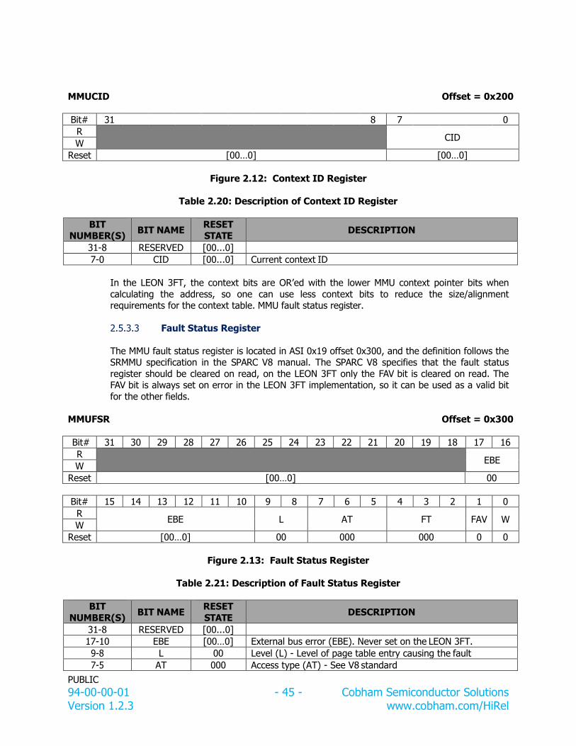
PUBLIC
94-00-00-01 - 45 - Cobham Semiconductor Solutions Version 1.2.3 www.cobham.com/HiRel
MMUCID Offset = 0x200
Bit# 31 8 7 0
R CID
W
Reset [00…0] [00…0]
Figure 2.12: Context ID Register
Table 2.20: Description of Context ID Register
BIT NUMBER(S)
BIT NAME RESET STATE
DESCRIPTION
31-8 RESERVED [00...0]
7-0 CID [00...0] Current context ID
In the LEON 3FT, the context bits are OR’ed with the lower MMU context pointer bits when
calculating the address, so one can use less context bits to reduce the size/alignment requirements for the context table. MMU fault status register.
Fault Status Register 2.5.3.3
The MMU fault status register is located in ASI 0x19 offset 0x300, and the definition follows the SRMMU specification in the SPARC V8 manual. The SPARC V8 specifies that the fault status
register should be cleared on read, on the LEON 3FT only the FAV bit is cleared on read. The FAV bit is always set on error in the LEON 3FT implementation, so it can be used as a valid bit
for the other fields.
MMUFSR Offset = 0x300
Bit# 31 30 29 28 27 26 25 24 23 22 21 20 19 18 17 16
R EBE
W
Reset [00…0] 00
Bit# 15 14 13 12 11 10 9 8 7 6 5 4 3 2 1 0
R EBE L AT FT FAV W
W
Reset [00…0] 00 000 000 0 0
Figure 2.13: Fault Status Register
Table 2.21: Description of Fault Status Register
BIT
NUMBER(S) BIT NAME
RESET
STATE DESCRIPTION
31-8 RESERVED [00...0]
17-10 EBE [00…0] External bus error (EBE). Never set on the LEON 3FT.
9-8 L 00 Level (L) - Level of page table entry causing the fault
7-5 AT 000 Access type (AT) - See V8 standard

PUBLIC
94-00-00-01 - 46 - Cobham Semiconductor Solutions Version 1.2.3 www.cobham.com/HiRel
BIT
NUMBER(S) BIT NAME
RESET
STATE DESCRIPTION
4-2 FT 000 Fault type (FT) – See Table 2.22.
1 FAV 0 Fault address valid (FAV) - cleared on read, always written
to 1 on fault
0 W 0 Overview (W) - multiple faults of the same priority encountered
Table 2.22: Fault Type
FT Fault Type
0 None
1 Invalid Address Error
2 Protection Error
3 Privilege Violation Error
4 Translation Error
5 Access Bus Error
6 Internal Error
Fault Address Register 2.5.3.4
The MMU fault address register is located in ASI 0x19 offset 0x400, and the definition follows the SRMMU specification in the SPARC V8 manual.
MMUFAR Offset = 0x400
Bit# 31 12 11 0
R FA
W
Reset [--…--] [00…0]
Figure 2.14: Fault Address Register
Table 2.23: Description of Fault Address Register
BIT NUMBER(S)
BIT NAME RESET STATE
DESCRIPTION
31-12 FA [00...0] Top bits of virtual address causing translation fault
11-0 RES [00...0]
Translation Look-Aside Buffer (TLB) 2.5.4
The MMU is configured to use a separate TLB for instructions and data. The number of entries is
eight for instructions and eight for data. The organization of the TLB and number of entries is
not visible to the software and does not require any modification to the operating system.
2.6 LEON 3FT Storage Allocation
Integer Unit Register File 2.6.1
The integer Unit register file has one write port and two read ports, all 32-bit wide. The register
file is protected with RAM blocks (Flip-Flops) in a TMR configuration.

PUBLIC
94-00-00-01 - 47 - Cobham Semiconductor Solutions Version 1.2.3 www.cobham.com/HiRel
Floating Point Unit (FPU) Register File 2.6.2
The FPU register file is protected with SEU hardened flip-flops.
Cache Memories 2.6.3
The following sections detail how cache information is stored in physical memory.
Instruction Cache Tags 2.6.3.1
The instruction tags are made up by 8 valid bits, 20 tag address bits, eight MMU context bits and four parity bits. A total of 40 bits are dedicated to each Instruction Cache line. There are a
total of 128 instruction tags. Instruction cache tags have the following allocation.
Table 2.24: Instruction Cache Tags
BITS USAGE
47-39 Unused and tied to ground
38-35 Parity Bit 38: XOR [35:20]
Bit 37: XOR [19:12]
Bit 36: XOR [11:8] Bit 35: XOR [7:0]
34-27 MMU context
26-8 Tag address
7-0 Valid
0: Word not valid
1: Word valid
Data Cache Tags 2.6.3.2
The data tags are made of one valid bit, 20 tag address bits, eight MMU context bits and four
parity bits. A total of 33 bits are dedicated for each Data Cache line. There are a total of 256 data tags. Data cache tags have the following allocation.
Table 2.25: Data Cache Tags
BITS USAGE
35-33 Unused and tied to ground
32-29 Parity
Bit 39: XOR [28:13] Bit 38: XOR [12:5]
Bit 30: XOR [4:1]
Bit 29: XOR [0]
28-21 MMU context
20-1 Tag address
0 Valid 0: Word not valid
1: Word valid

PUBLIC
94-00-00-01 - 48 - Cobham Semiconductor Solutions Version 1.2.3 www.cobham.com/HiRel
Data Snoop Tags 2.6.3.3
The data snoop tags are made up by 20 tag address bits and one parity bit. A total of 21 bits
are dedicated for each data snoop line. The bits are located as follows: tag address [19:0], parity [20].
Instruction and Data Cache Memory 2.6.3.4
The data part of the instruction and data caches consist of 32-data bits and four parity bits. The bits are allocated as follows:
Table 2.26: Data Cache Tags
BITS USAGE
39-36 Unused and tied to ground
35-32 Parity
Bit 35: XOR [31:24] Bit 34: XOR [23:16]
Bit 33: XOR [15:8]
Bit 32: XOR [7:0]
31-0 Data

PUBLIC
94-00-00-01 - 49 - Cobham Semiconductor Solutions Version 1.2.3 www.cobham.com/HiRel
Memory Controller with EDAC Chapter 3:
3.1 Overview
The memory controller provides a bridge between external memory and the AHB bus. The memory controller handles four types of devices: PROM, Asynchronous Static Ram (SRAM),
Synchronous Dynamic Ram (SDRAM) and memory mapped Input/Output (I/O) devices. The
PROM, SRAM and SDRAM areas can be EDAC-protected using a (39, 7) BCH code. The EDAC provides single-error correction and double-error detection for each 32-bit memory word.
The SDRAM area can optionally also be protected using Reed-Solomon coding. In this case, a
16-bit checksum is used for each 32-bit word and any two adjacent 4-bit (nibble) errors can be corrected.
The memory controller is configured through three configuration registers accessible via an APB bus interface. The external data bus can be configured in 8, 16, or 32-bit mode depending on
application requirements. The controller decodes three address spaces on the AHB bus (PROM, I/O, and SRAM/SDRAM).
External chip-selects are provided for two PROM banks, one I/O bank, five SRAM banks and two SDRAM banks. Figure 3.1 below shows how the notional connection to the different device
types is made.
Figure 3.1: FTMCTRL Connected to Different Types of Memory Devices
3.2 PROM Access

PUBLIC
94-00-00-01 - 50 - Cobham Semiconductor Solutions Version 1.2.3 www.cobham.com/HiRel
A read access to PROM consists of two data cycles and between 0 and 30 wait states. The read
data (and optional EDAC check-bits CB[6:0]) are latched on the rising edge of the clock on the last data cycle. On non-consecutive accesses, a lead-out cycle is added after a read cycle to
prevent bus contention due to slow turn-off time of PROM devices. See Section 3.16 for timing diagram examples of PROM accesses.
3.3 Memory Mapped I/O
Accesses to I/O have similar timing to the PROM accesses. The I/O select (IOS) and output
enable (OE) signals are delayed one clock to allow for a stable address before it is asserted.
See Section 3.16 for timing diagram examples of I/O accesses.
3.4 SRAM Access
The SRAM area is divided up to five RAM banks. The size of banks 1-4 (RAMS[3: 0]) is
programmed in the RAM bank-size field (MCFG2[12:9]) and can be set in binary steps from 8
Kbyte to 256 Mbyte. The fifth bank (RAMS[4]) decodes the upper 512 Mbyte. A read access to
SRAM consists of two data cycles and between zero and three waitstates. The read data (and optional EDAC check-bits CB[6:0]) are latched on the rising edge of the clock on the last data
cycle. Accesses to RAMS[4] can further be stretched by de-asserting BRDY until the data is
available. On non-consecutive accesses, a lead-out cycle is added after a read cycle to prevent bus contention due to slow turn-off time of memories. See Section 3.16 for timing diagram
examples of SRAM accesses.
For read accesses to RAMS[4: 0], a separate output enable signal, RAMOE[n] is provided for
each RAM bank and only asserted when that bank is selected. A write access is similar to the read access, but takes a minimum of three cycles.
Each byte lane has an individual write strobe to allow efficient byte and half-word writes. If the
memory uses a common write strobe for the full 16 or 32-bit data, the read-modify-write bit
MCFG2 should be set to enable read-modify-write cycles for sub-word writes. See Section 3.16 for timing diagram examples of SRAM accesses.
3.5 8-bit and 16-bit PROM and SRAM Access
To support applications with low memory and performance requirements efficiently, the SRAM and PROM areas can be individually configured for 8-bit or 16-bit operation by programming the
ROM and RAM size fields in the memory configuration registers. Since read access to memory is always done on 32-bit word basis, read access to 8-bit memory is transformed in a burst of
four read cycles while access to 16-bit memory generates a burst of two 16-bits reads. During
writes, only the necessary bytes will be written. The following figures show interface examples with 8-bit, 16-bit, and 32-bit PROM and SRAM.
The read-modify-write (RM) bit in MCFG2 must NOT be set if RAM EDAC is disabled when RAM
width is set to 8-bit.
If the PROM is configured in 8-bit mode, EDAC protection is provided in a similar way as for the
SRAM memory described above. The difference is that write accesses are not being handled automatically. Instead, write accesses must only be performed as individual byte accesses by
the software, writing one byte at a time, and the corresponding checkbit byte must be calculated and be written to the correct locations by the software.

PUBLIC
94-00-00-01 - 51 - Cobham Semiconductor Solutions Version 1.2.3 www.cobham.com/HiRel
An additional lead-out cycle (i.e. 2 in total) is added to writes in the PROM area. In 8-bit mode,
the additional cycle is added to the last of the consecutive
Figure 3.2: 8-bit Memory Interface Example

PUBLIC
94-00-00-01 - 52 - Cobham Semiconductor Solutions Version 1.2.3 www.cobham.com/HiRel
Figure 3.3: 16-bit Memory Interface Example
PROMCSOEWE
A D CB
SRAMCSOEWE
A D CB
A[27:2]
CB[7:0]
A[27:2]
D[31:0]
CB[7:0]
D[31:0]
A D CB
ADDR[27:0]DATA[31:0]
CB[7:0]
ROMOE[4:0]
ROMS[0]
WRITE
RAMS[4:0]
RAMOE[4:0]
RWE[3:0]
MemoryController
32-bit RAM
32-bit PROM
Figure 3.4: 32-bit Memory Interface Example
In 8-bit mode, the PROM/SRAM devices should be connected to the data bus DATA[31:24]. The
LSB address bus should be used for addressing (ADDR[25:0]). In 16-bit mode, DATA[31:16] should be used as data bus and ADDR[26:1] as address bus. EDAC protection is not available in
16-bit mode.
3.6 8-bit and 16-bit I/O Accesses Similar to the PROM/SRAM areas, the I/O area can also be configured to 8-bit or 16-bit mode.
However, the I/O device will not be accessed by multiple 8/16 bit accesses as the memory
areas, but only with one single access just as in 32-bit mode. To access an I/O device on an 8-bit bus, LDUB/STB instructions should be used. To access an I/O device on a 16-bit bus,
LDUH/STH instructions should be used.
3.7 Burst Cycles To improve the bandwidth of the memory bus, accesses to consecutive addresses can be
performed in burst mode. Burst transfers will be generated when the memory controller is accessed using an AHB burst request. These include instruction cache-line fills, double loads
and double stores. The timing of a burst cycle is identical to the programmed basic cycle with
the exception that during read cycles, the lead-out cycle will only occur after the last transfer. Burst cycles will not be generated to the I/O area.
3.8 SDRAM Access

PUBLIC
94-00-00-01 - 53 - Cobham Semiconductor Solutions Version 1.2.3 www.cobham.com/HiRel
General 3.8.1
Synchronous Dynamic RAM (SDRAM) access is supported to two banks of PC100/PC133
compatible devices. The SDRAM controller supports 64 MB, 256 MB and 512 MB devices with 8-12 column-address bits and up to 13 row-address bits. The size of the two banks can be
programmed in binary steps between 4 Mbyte and 512 Mbyte. The SDRAM controller operation
is controlled through MCFG2 and MCFG3. A 32-bit data bus width is supported that can interface 64-bit DIMM modules. The memory controller can be configured to use either a
shared or separate bus connecting the controller and SDRAM devices. See Section 3.17 for timing diagram examples of SDRAM accesses.
Address Mapping 3.8.2
Two SDRAM chip-select signals are used for address decoding. SDRAM is memory mapped into the upper half of the RAM area (0x60000000+) by setting the DE bit to 1 and SI bit to 0 in
memory configuration Register 2 (MCFG2). SDRAM is memory mapped into the lower half of the RAM area (0x40000000+) by setting the DE bit to 1 and SI bit to 1 in the MCFG2 register.
Initialization 3.8.3
When the SDRAM controller is enabled, it automatically performs the SDRAM initialization sequence of one PRECHARGE command, eight AUTO-REFRESH command and LOAD-MODE-
REG command on both banks simultaneously. The controller programs the SDRAM to use line burst on read and single location access on write.
Configurable SDRAM Timing Parameters 3.8.4
To provide optimum access cycles for different SDRAM devices (and at different frequencies), three SDRAM parameters can be programmed via MCGF2: TCAS, TRP and TRFC. The value of
these fields affect the SDRAM timing as described in Table 3.1.
Table 3.1: SDRAM Programmable Minimum Timing Parameters
SDRAM TIMING PARAMETER MINIMUM TIMING CLOCKS
CAS latency, RAS/CAS delay (tCAS, tRCD) TCAS + 2
Precharge to activate (tRP) TRP + 2
Auto-refresh command period (tRFC) TRFC + 3
Activate to precharge (tRAS) TRFC + 1
Activate to Activate (tRC) TRP + TRFC + 4
If the TCAS, TRP and TRFC are programmed such that the PC100/133 specifications are fulfilled, the remaining SDRAM timing parameters will also be met. The Table 3.2 below shows
typical settings for 100 and 133 MHz operation and the resulting SDRAM timing (in ns).
Table 3.2: SDRAM Programmable Minimum Timing Parameters
SDRAM SETTINGS tCAS tRC tRP tRFC tRAS
100 MHz, CL=2; TRP=0, TCAS=0, TRFC=4 20 80 20 70 50
100 MHz, CL=3; TRP=0, TCAS=1, TRFC=4 30 80 20 70 50
133 MHz, CL=2; TRP=1, TCAS=0, TRFC=6 15 82 22 67 52
133 MHz, CL=3; TRP=1, TCAS=1, TRFC=6 22 82 22 67 52

PUBLIC
94-00-00-01 - 54 - Cobham Semiconductor Solutions Version 1.2.3 www.cobham.com/HiRel
3.9 Refresh The SDRAM controller contains a refresh function that periodically issues an AUTO-REFRESH
command to both SDRAM banks. The period between the commands (in clock periods) is programmed in the refresh counter reload field in the MCFG3 register. Depending on SDRAM
type, the required period is typically 7.8 or 15.6ms (corresponding to 780 or 1560 clocks at 100
MHz). The generated refresh period is calculated as follows:
refresh period = ((reload value) + 1) / sysclk
The refresh function is enabled by setting bit 31 in MCFG2.
SDRAM Commands 3.9.1
The controller can issue three SDRAM commands by writing to the SDRAM command field in
MCFG2: PRE-CHARGE, AUTO-REFRESH and LOAD-MODE-REG (LMR). If the LMR command is issued, the CAS delay as programmed in MCFG2 will be used and remaining fields are fixed:
page read burst, single location write, and sequential burst. The command field clears after a
command has been executed. When changing the value of the CAS delay, a LOAD-MODE-REGISTER command should be generated at the same time.
Note: When issuing SDRAM commands, the SDRAM refresh must be disabled.
Read Cycles 3.9.2
A read cycle is started by performing an ACTIVATE command to the desired bank and row,
followed by a READ command after the programmed CAS delay. A read burst is performed if a burst access has been requested on the AHB bus. The read cycle is terminated with a PRE-
CHARGE command; no banks are left open between two accesses.
Write Cycles 3.9.3
Write cycles are performed similarly to read cycles, but WRITE commands are issued after
activation. A write burst on the AHB bus generates a burst of write commands without idle cycles in between.
Address Bus 3.9.4
The memory controller uses a common address bus for PROM, I/O, SRAM and SDRAM. SDRAM connected to the address bus should use ADDR[14:2] for the row select and ADDR[16:15] for
the bank select.
Data Bus 3.9.5
The memory controller uses a common address bus for PROM, I/O, SRAM and SDRAM. The
SDRAM uses a 32-bit data bus and can access a 64-bit SDRAM at half the data capacity.
Clocking 3.9.6
The SDRAM memory is clocked by the SDCLK output. This output is in phase with the internal
system clock and provides the maximum margin for setup and hold on the external signals. The SDCLK output will be available as long as the system clock is operating.

PUBLIC
94-00-00-01 - 55 - Cobham Semiconductor Solutions Version 1.2.3 www.cobham.com/HiRel
Initialization 3.9.7
Each time the SDRAM is enabled (by setting bit 14 in MCFG2), an SDRAM initialization
sequence will be sent to both SDRAM banks. The sequence consists of one PRECHARGE command, eight AUTO-REFRESH commands and one LOAD-COMMAND-REGISTER command.
3.10 Memory EDAC
BCH EDAC 3.10.1
The FTMCTRL is provided with an error detection and correction (EDAC) controller that can
correct one-bit-error and detect two-bit-errors in a 32-bit word. For each word, a 7-bit checksum is generated according to the equations below. A correctable error will be handled
transparently by the memory controller, but will add one waitstate to the access. If an un-correctable error (double-error) is detected, the current AHB cycle will end with an error
response. The EDAC can be used during access to PROM, SRAM, and SDRAM areas by setting the corresponding EDAC enable bits in the MCFG3 register. The equations below show how the
EDAC checkbits are generated:
CB0 = D0 ^ D4 ^ D6 ^ D7 ^ D8 ^ D9 ^ D11 ^ D14 ^ D17 ^ D18 ^ D19 ^ D21 ^ D26 ^ D28 ^ D29 ^ D31 CB1 = D0 ^ D1 ^ D2 ^ D4 ^ D6 ^ D8 ^ D10 ^ D12 ^ D16 ^ D17 ^ D18 ^ D20 ^ D22 ^ D24 ^ D26 ^ D28
CB2 = D0 ^ D3 ^ D4 ^ D7 ^ D9 ^ D10 ^ D13 ^ D15 ^ D16 ^ D19 ^ D20 ^ D23 ^ D25 ^ D26 ^ D29 ^ D31
CB3 = D0 ^ D1 ^ D5 ^ D6 ^ D7 ^ D11 ^ D12 ^ D13 ^ D16 ^ D17 ^ D21 ^ D22 ^ D23 ^ D27 ^ D28 ^ D29 CB4 = D2 ^ D3 ^ D4 ^ D5 ^ D6 ^ D7 ^ D14 ^ D15 ^ D18 ^ D19 ^ D20 ^ D21 ^ D22 ^ D23 ^ D30 ^ D31 CB5 = D8 ^ D9 ^ D10 ^ D11 ^ D12 ^ D13 ^ D14 ^ D15 ^ D24 ^ D25 ^ D26 ^ D27 ^ D28 ^ D29 ^ D30 ^ D31 CB6 = D0 ^ D1 ^ D2 ^ D3 ^ D4 ^ D5 ^ D6 ^ D7 ^ D24 ^ D25 ^ D26 ^ D27 ^ D28 ^ D29 ^ D30 ^ D31
If the memory is configured in 8-bit mode, the EDAC checkbit bus (CB[7:0]) is not used, but it is still possible to use EDAC protection. This is done by allocating the top 20% of the memory
bank to the EDAC checksums. If the EDAC is enabled, a read access reads the data bytes from the nominal address and the EDAC checksum from the top part of the bank. A write cycle is
performed the same way in the SRAM memory region. In this way, 80% of the bank memory is
available as program or data memory while the top 20% is used for check bits. The size of the memory bank is determined from the settings in MCFG1 and MCFG2. The EDAC cannot be used
on memory areas configured in 16-bit mode.
The operation of the EDAC can be tested trough the MCFG3 register. If the WB (write bypass)
bit is set, the value in the TCB field replaces the normal checkbits during memory write cycles. If the RB (read bypass) is set, the memory checkbits of the loaded data will be stored in the TCB
field during memory read cycles.
Note:
1) When the EDAC is enabled, the RMW bit in memory configuration register 2 must be set. 2) In the PROM memory region, checkbit bytes are written using external tools, MKPROM2
and GRMON2.
Reed-Solomon EDAC 3.10.2
The Reed-Solomon EDAC provides block error correction and is capable of correcting up to two
4-bit nibble errors in a 32-bit data word or 16-bit checksum. The Reed-Solomon EDAC can be enabled for the SDRAM area only and uses a 16-bit checksum. Operation and timing is identical
to the BCH EDAC with the pipeline option enabled. The Reed-Solomon EDAC is enabled by setting the RSE and RE bits in MCFG3 and the RMW bit in MCFG2.

PUBLIC
94-00-00-01 - 56 - Cobham Semiconductor Solutions Version 1.2.3 www.cobham.com/HiRel
The Reed-Solomon data symbols are 4-bit wide, represented as GF(2^4). The basic Reed-
Solomon code is a shortened RS(15, 13, 2) code, represented as RS(6, 4, 2). It has the capability to detect and correct a single symbol error anywhere in the codeword. The EDAC
implements an interleaved RS(6, 4, 2) code where the overall data is represented as 32 bits and the overall checksum is represented as 16 bits. The codewords are interleaved nibble-wise.
The interleaved code can correct two 4-bit errors when each error is located in a nibble and not
in the same original RS(6, 4, 2) codeword.
The Reed-Solomon RS(15, 13, 2) code has the following definition:
there are 4 bits per symbol;
there are 15 symbols per codeword;
the code is systematic;
the code can correct one symbol error per codeword;
the field polynomial is:
f(x) = x4 + x + 1
the code generator polynomial is:
𝑔(𝑥) = ∏ (𝑥 + 𝑎𝑖 8
𝑖=0 ) = ∑ 𝑔𝑗2𝑗=0 ∙ 𝑥𝑗
for which the highest power of x is stored first; a codeword is defined as 15 symbols:
c0, c1, c2, c3, c4, c5, c6, c7, c8, c9, c10, c11, c12, c13, c14
where c0 to c12 represent information symbols and c13 to c14 represent check
symbols.
The shortened and interleaved RS(6, 4, 2) code has the following definition:
the codeword length is shortened to 4 information symbols and 2 check symbols and
as follows:
c0 = c1 = c2 = c3 = c4 = c5 = c6 = c7 = c8 = 0
where the above information symbols are suppressed or virtually filled with zeros;
two codewords are interleaved (i.e. interleaved depth I=2) with the following
mapping to the 32-bit data and 16-bit checksum, were ci,j is a symbol with codeword index i and symbol index j:
c0,9 = DATA[31:28]
c1,9 = DATA[27:24]
c0,10 = DATA[23:20]
c1,10 = DATA[19:16]
c0,11 = DATA[15:12]
c1,11 = DATA[11:8]
c0,12 = DATA[7:4]
c1,12 = DATA[3:0]

PUBLIC
94-00-00-01 - 57 - Cobham Semiconductor Solutions Version 1.2.3 www.cobham.com/HiRel
c0,13 = CB[15:12]
c1,13 = CB[11:8]
c0,14 = CB[7:4]
c1,14 = CB[3:0]
Note: The Reed-Solomon EDAC ONLY supports 32-bit wide SDRAM buses.
EDAC Error Reporting 3.10.3
An un-correctable EDAC error results in an AHB error response. The initiating AHB master will
be notified of the error and take corresponding action. If the master was the LEON 3FT microprocessor, an instruction or data error trap will be taken (see Section Chapter 2:). The
AHB error response will also be registered in the AHB status register. Correctable EDAC errors are handled transparently and are not visible on the AHB bus. They are registered in the AHB
status register through the use of a sideband signal. This can be used for providing an external scrubbing mechanism and/or error statistics. The correctable error signal is connected to the
AHB status register which monitors the correctable error signal and error responses on the bus.
Please see the AHB status register section for more information.
3.11 Using 𝐁𝐑𝐃𝐘
The BRDY signal can be used to stretch access cycles to the PROM and I/O areas and the
SRAM area decoded by RAMS[4]. The accesses will always have at least the pre-programmed
number of waitstates as defined in registers MCFG1 and MCFG2, but will be further stretched
until BRDY is asserted. BRDY should be asserted in the cycle preceding the last one. If bit 29 in
MCFG1 is set, BRDY can be asserted asynchronously with the system clock. In this case, the
read data must be kept stable until the de-assertion of OE/RAMOE. BRDY must be asserted for
at least 1.5 clock cycles. The use of BRDY can be enabled separately for the PROM, I/O and
RAMS[4] areas. It is recommended that BRDY remain asserted until the corresponding chip
select signal is de-asserted to ensure that the access has been properly completed and to avoid
a datapath stall. See Section 3.16 for timing diagram examples with BRDY.
3.12 Access Errors
An access error can be signaled by asserting the BEXC signal which is sampled with the data. If
the usage of BEXC is enabled in register MCFG1, an error response generates on the internal
AHB bus. BEXC can be enabled or disabled through register MCFG1 and is active for all areas
(PROM, I/O an RAM). For writes, it is sampled on the last rising edge before chip select is de-
asserted which is controlled by means of waitstates or bus ready signaling. BEXC is only sampled
in the last access for 8-bit mode for RAM and PROM. When four bytes are written for a word
access to 8-bit wide memory BEXC is only sampled in the last access with the same timing as
a single access in 32-bit mode. See Section 3.16 for timing diagram examples using BEXC.
3.13 Attaching an External DRAM Controller
To attach an external DRAM controller, RAMS[4] should be used since it allows the cycle time
to vary through the use of BRDY. In this way, delays can be inserted as required for opening of
banks and refresh.

PUBLIC
94-00-00-01 - 58 - Cobham Semiconductor Solutions Version 1.2.3 www.cobham.com/HiRel
3.14 Registers The core is programmed through registers mapped into APB address space.
Table 3.3: FTMCTRL Memory Controller Registers
REGISTER APB ADDRESS
Memory configuration register 1 (MCFG1) 0x80000000
Memory configuration register 2 (MCFG2) 0x80000004
Memory configuration register 3 (MCFG3) 0x80000008
Memory configuration register 4 (MCFG4) 0x8000000C
Memory Configuration Register 1 (MCFG1) 3.14.1
Memory configuration register 1 is used to program the timing of ROM and I/O accesses.
MCFG 1 Address = 0x8000_0000
Bit# 31 30 29 28 27 26 25 24 23 22 21 20 19 18 17 16
R PB AB IBW[1:0] IB BE
IW[3:0] IE
PZ[3:2]
W
Reset 0 0 0 -- 0 0 0 0000 0 0 11
Bit# 15 14 13 12 11 10 9 8 7 6 5 4 3 2 1 0
R PZ[1:0] PE
PD[1:0] PW[3:0] PR[3:0]
W
Reset 11 00 0 -- GPIO[1:0] 1111 1111
Figure 3.5: Memory Configuration Register 1
Table 3.4: Description of Memory Configuration Register 1
BIT
NUMBER(S) BIT NAME
RESET
STATE DESCRIPTION
31 RESERVED 0 30 PB 0 PROM area bus enable
0: BRDY disabled for PROM area.
1: BRDY enabled for PROM area.
29 AB 0 Asynchronous bus ready 0: BRDY is synchronous relative to system clock.
1: BRDY input can be asserted without relation to the system clock.
28-27 IBW _ I/O data bus width
00: 8 bits 01: 16 bits
10: 32 bits
11: Not used
26 IB 0 I/O area bus ready enable
0: BRDY disabled for I/O area. 1: BRDY enabled for I/O area.
25 BE 0 Bus error enable

PUBLIC
94-00-00-01 - 59 - Cobham Semiconductor Solutions Version 1.2.3 www.cobham.com/HiRel
BIT
NUMBER(S) BIT NAME
RESET
STATE DESCRIPTION
0: BEXC disabled 1: BEXC enabled
24 RESERVED 0 23-20 IW 0000 Number of waitstates during I/O accesses
0000: 0 waitstates 0001: 1 waitstates
0010: 2 waitstates ...
1111: 15 waitstates
19 IE 0 I/O enable 0: Access to memory mapped I/O space is disabled
1: Access to memory mapped I/O space is enabled
18 RESERVED 0 17-14 PZ 1111 PROM size is fixed
1111: 256MB
13-12 RESERVED 00 11 PE 0 PROM write enable
0: PROM write cycles disabled 1: PROM write cycles enabled
10 RESERVED 0 9-8 PD GPIO
[1:0]
Data width of the PROM area
PWIDTH is set to the value GPIO[1:0] following a reset.
00: 8 bits 01: 16 bits
10: 32 bits 11: Not used
7-4 PW 1111 Number of waitstates during PROM write cycles
PWS is set to the maximum value of 15 which equals 30 wait- states following a reset.
0000: 0 0001: 2
0010: 4
... 1111: 30
3-0 PR 1111 Number of waitstates during PROM read cycles PRS is set to the maximum value of 15 which equals 30
waitstates following a reset.
0000: 0 0001: 2
0010: 4 ...
1111: 30
Memory Configuration Register 2 (MCFG2) 3.14.2
Memory configuration register 2 is used to control the timing of the SRAM and SDRAM.

PUBLIC
94-00-00-01 - 60 - Cobham Semiconductor Solutions Version 1.2.3 www.cobham.com/HiRel
MCFG2 Address = 0x8000_0004
Bit# 31 30 29 28 27 26 25 24 23 22 21 20 19 18 17 16
R DR DP DF[2:0] DC DZ[2:0] DS[1:0] DD[1:0]
BW PB
W
Reset 0 1 111 1 000 10 00 0 0 0
Bit# 15 14 13 12 11 10 9 8 7 6 5 4 3 2 1 0
R DE SI SZ[3:0] SB RM SD[1:0] SW[1:0] SR[1:0]
W
Reset 0 0 0 -- 0 0 - -- 00 00
Figure 3.6: Memory Configuration Register 2
Table 3.5: Description of Memory Configuration Register 2
BIT
NUMBER(S) BIT NAME
RESET
STATE DESCRIPTION
31 DR 0 SDRAM refresh 0: SDRAM refresh disable
1: SDRAM refresh enabled
30 DP 1 SDRAM TRP parameter 0: tRP = 2 system clocks
1: tRP = 3 system clocks
29-27 DF 111 SDRAM TRFC parameter tRFC = 3 + DF system clocks
26 DC 1 SDRAM CAS parameter When changed, a LOAD-COMMAND-REGISTER command must
be issued at the same time and also sets RAS/CAS
delay (tRCD). 0: CAS = 2 cycle delay
1: CAS = 3 cycle delay
25-23 DZ 000 Bank size for SDRAM chip selects defined as 4MB*2DZ
000: 4MB 001: 8MB
010: 16MB
... 111: 512MB
22-21 DS 10 SDRAM column size is 4096 when bits [25:23] = 111
Otherwise, the column size is defined as: 00: 256
01: 512 10: 1024
11: 2048
20-19 DD 00 SDRAM command Writing a non-zero value generates an SDRAM command.
The field is reset to 00b after command has been executed. 01: PRECHARGE
10: AUTO-REFRESH
11: LOAD-COMMAND-REGISTER
18 BW 0 Memory controller data bus width.

PUBLIC
94-00-00-01 - 61 - Cobham Semiconductor Solutions Version 1.2.3 www.cobham.com/HiRel
BIT
NUMBER(S) BIT NAME
RESET
STATE DESCRIPTION
0: 32-bit 1: 64-bit
Read=0; Write=don’t care.
17 PB 0 SDRAM Page Burst
No Supported
16-15 RESERVED 00 14 DE 0 SDRAM enable
0: SDRAM controller disabled 1: SDRAM controller enabled
13 SI 0 SRAM disable If set together with bit 14 the SRAM can be disabled.
DE=0
x: SRAM enabled DE=1 0: SRAM enabled
1: SRAM disabled x=don’t care
12-9 SZ -- Size of each SRAM bank as 8*2SZ KB 0000: 8KB 0001: 16KB 0010: 32KB
...
1111: 256MB
8 RESERVED 0 7 SB 0 SRAM area bus ready enable
0: BRDY disabled for SRAM area
1: BRDY enabled for SRAM area
6 RM -- Enable read-modify-write cycles on sub-word writes to 16-
and 32-bit areas with common write strobe (no byte write
strobe). 0: Disabled
1: Enabled
5-4 SD -- Data width of the SRAM area 00: 8 01: 16
1x: 32 x=don’t care
3-2 SW 00 Number of waitstates during SRAM write cycles
00: 0 01: 1
10: 2 11: 3
1-0 SR 00 Number of waitstates during SRAM read cycles
00: 0 01: 1
10: 2 11: 3
Memory Configuration Register 3 (MCFG3) 3.14.3
MCFG3 contains the reload value for the SDRAM refresh counter and to control and monitor the
memory EDAC. It also contains the configuration of the register file EDAC.

PUBLIC
94-00-00-01 - 62 - Cobham Semiconductor Solutions Version 1.2.3 www.cobham.com/HiRel
MCFG3 Address = 0x8000_0008
Bit# 31 30 29 28 27 26 25 24 23 22 21 20 19 18 17 16
R RSE
ME RLVAL[14:4]
W
Reset 000 0 1 [--…-]
Bit# 15 14 13 12 11 10 9 8 7 6 5 4 3 2 1 0
R RLVAL[3:0] WB RB SE PE TCB[7:0]
W
Reset -- 0 0 -- GPIO[2] [--…-]
Figure 3.7: Memory Configuration Register 3
Table 3.6: Description of Memory Configuration Register 3
BIT
NUMBER(S) BIT NAME
RESET
STATE DESCRIPTION
31-29 RESERVED 000 28 RSE 0 Reed-Solomon EDAC
0: BCH EDAC available for SDRAM
1: Reed-Solomon EDAC available for SDRAM
27 ME 1 Memory EDAC Indicates if memory EDAC is present Read = 1;
Write = Don’t care
26-12 RLDVAL [--...-] SDRAM refresh counter reload value The period between each AUTO-REFRESH command is
calculated as follows: tREFRESH = (RLDVAL + 1) / SYS_CLK
11 WB 0 EDAC diagnostic write bypass
0: Normal operation
1: EDAC write bypassed
10 RB 0 EDAC diagnostic read bypass
0: Normal operation
1: EDAC read bypassed
9 R - Enable EDAC checking of the SDRAM or SRAM area
0: EDAC checking of the RAM area disabled 1: EDAC checking of the RAM area enabled
8 PE GPIO [2] Enable EDAC checking of the PROM area
At reset, this bit is initialized with the value GPIO[2]. 0: EDAC checking of the PROM area disabled
1: EDAC checking of the PROM area enabled
7-0 TCB[7:0] [--...-] Test checkbits This field replaces the normal checkbits during store cycles
when WB (bit 11) is set. TCB is also loaded with the memory checkbits during load cycles when RB (bit 10) is set.
Memory Configuration Register 4 (MCFG4) 3.14.4
MCFG4 provides the means to insert Reed-Solomon EDAC errors into memory for diagnostic
purposes.

PUBLIC
94-00-00-01 - 63 - Cobham Semiconductor Solutions Version 1.2.3 www.cobham.com/HiRel
MCFG4 Address = 0x8000_000C
Bit# 31 30 29 28 27 26 25 24 23 22 21 20 19 18 17 16
R WB
W
Reset [00…0] 0
Bit# 15 14 13 12 11 10 9 8 7 6 5 4 3 2 1 0
R RTCB[15:0]
W
Reset [--…-]
Figure 3.8: Memory Configuration Register 4
Table 3.7: Description of Memory Configuration Register 4
BIT
NUMBER(S) BIT NAME
RESET
STATE DESCRIPTION
31-17 RESERVED [00…0]
16 WB 0 Reed Solomon EDAC diagnostics write bypass 0: Normal
1: EDAC write bypasses
15-0 RTCB[15:0] [--...-] Reed Solomon test checkbits This field replaces the normal check bits during write cycles
when WB is set.
3.15 Boot Strap Configuration
Upon power up or external RESET, GPIO[2] is configured as an input and a high logic level
seen on this pin when RESET goes high configures the PROM to operate with EDAC enable.
Upon power up or external RESET, GPIO[1:0] is configured as an input and the following logic
level combinations on each pin when RESET goes high to configure the PROM data width:
Table 3.8: Logic Level Combinations
GPIO[1:0] PROM Data width
00 8-bit
01 16-bit
10 32-bit
3.16 PROM, SRAM, and Memory Mapped I/O Timing Diagrams This section shows typical timing diagrams for PROM, SRAM and I/O accesses. These timing
diagrams are functional, and are intended to show the relationship between control signals and SDCLK. The actual value of the timing parameters can be found in Chapter 4 of the
UT699E/UT700 datasheet.

PUBLIC
94-00-00-01 - 64 - Cobham Semiconductor Solutions Version 1.2.3 www.cobham.com/HiRel
Figure 3.9: PROM and SRAM 32-bit Read
Figure 3.10: PROM and SRAM 32-bit Read Cycle Consecutive

PUBLIC
94-00-00-01 - 65 - Cobham Semiconductor Solutions Version 1.2.3 www.cobham.com/HiRel
Figure 3.11: PROM and SRAM 32-bit Read Cycle with Waitstates and 𝐁𝐑𝐃𝐘
Figure 3.12: PROM and SRAM 32-bit Read Cycle with Waitstates and Asynchronous 𝐁𝐑𝐃𝐘

PUBLIC
94-00-00-01 - 66 - Cobham Semiconductor Solutions Version 1.2.3 www.cobham.com/HiRel
Figure 3.13: PROM and SRAM 16-bit Read Cycle
Figure 3.14: PROM and SRAM 8-bit Read Cycle
t5
Data1 Data2
Lead-Out Lead-Out
SDCLK
t1 t1
ROMS[1:0] RAMS[4:0]
t1 t1
OE RAMOE[4:0]
READ
WRITE
RWE[3:0]
t1 t1 t1 t1
ADDR[27:1]
t6 t6
t5
DATA[31:16]
t6 t6
t5 t5
CB[7:0]

PUBLIC
94-00-00-01 - 67 - Cobham Semiconductor Solutions Version 1.2.3 www.cobham.com/HiRel
Figure 3.15: PROM and SRAM 32-bit Write Cycle on a 32-bit Bus
Figure 3.16: PROM and SRAM 16-bit Write Cycle on a 16-bit Bus
* ADDR[27:0] and DATA[31:24] and RWE[0] are used for 8-bit bus architecture.

PUBLIC
94-00-00-01 - 68 - Cobham Semiconductor Solutions Version 1.2.3 www.cobham.com/HiRel
Figure 3.17: Memory Mapped I/O 32-bit Read Cycle
Figure 3.18: Memory Mapped I/O 16-bit Read Cycle

PUBLIC
94-00-00-01 - 69 - Cobham Semiconductor Solutions Version 1.2.3 www.cobham.com/HiRel
Figure 3.19: Memory Mapped I/O 8-bit Read Cycle
Figure 3.20: Memory Mapped I/O 32-bit Write Cycle
* ADDR[27:0] and Data[31:24] are used for 16-bit I/O bus configurations. ADDR[27:0] and
DATA[31:24] for 8-bit I/O bus configurations.

PUBLIC
94-00-00-01 - 70 - Cobham Semiconductor Solutions Version 1.2.3 www.cobham.com/HiRel
3.17 SDRAM Timing Diagram This section shows typical timing diagrams for PROM, SRAM and I/O accesses. These timing
diagrams are functional and are intended to show the relationship between control signals and SDCLK. The actual values of the timing parameters can be found in Chapter 4 of the
UT699E/UT700 datasheet.
PUBLIC
94-00-00-01 - 71 - Cobham Semiconductor Solutions Version 1.2.3 www.cobham.com/HiRel
AHB Status Registers Chapter 4:
4.1 Overview
The AHB status registers store information about AHB accesses triggering an error response. There is a status register (AHB- STAT) and a failing address register (AHBADDR). Both are
contained in a module accessed from the APB bus.
4.2 Operation The AHB status module monitors AHB bus transactions and stores the current HADDR, HWRITE,
HMASTER and HSIZE internally. It is automatically enabled after power-on reset and monitors
the AHB bus until an error response (HRESP = “01”) is detected. When the error is detected, the status and address register content is frozen and the New Error (NE) bit is set to one. At
the same time interrupt 1 is generated. To start monitoring the bus again, the NE bit must be cleared by software.
The status registers are also frozen when the memory controller signals a correctable error
even though HRESP is “00” in this case. The software can then scrub the corrected address in
order to prevent error build-up and un-correctable multiple errors.
4.3 Correctable Errors
Error responses on the AHB bus can be detected. The FT memory controller has a correctable
error signal which is asserted each time a correctable error is detected. When such an error is detected, the effect will be the same as for an AHB error response. The only difference is that
the Correctable Error (CE) bit in the status register is set to one when a correctable error is detected.
When the CE bit is set the interrupt routine can acquire the address containing the correctable error from the failing address register and correct it. Clearing the NE bit resets the CE bit and
the monitoring becomes active again. Interrupt handling is described in detail in the following section.
4.4 Interrupts
The interrupt is connected to the interrupt controller to inform the processor of the error condition. The normal procedure is that an interrupt routine handles the error with the aid of
the information in the status registers. When it is finished it resets the NE bit and the monitoring becomes active again. Interrupts are generated for both AMBA error responses and
correctable errors as described above.
4.5 Registers Figure 4.1 and Figure 4.2 show the status register and failing address register. The registers
are accessed from the APB bus.

PUBLIC
94-00-00-01 - 72 - Cobham Semiconductor Solutions Version 1.2.3 www.cobham.com/HiRel
AHBSTAT Address = 0x8000_0F00
Bit# 31 30 29 28 27 26 25 24 23 22 21 20 19 18 17 16
R
W
Reset [--…-]
Bit# 15 14 13 12 11 10 9 8 7 6 5 4 3 2 1 0
R CE NE HW HM[3:0] HS[2:0]
W
Reset [--…-] 0 0 0 0000 000
Figure 4.1: AHB Status Register
Table 4.1: AHB Status Register Description
BIT
NUMBER(S) BIT NAME
RESET
STATE DESCRIPTION
31-10 RESERVED --
9 CE 0 Correctable error. Set if the memory controller signaled a
correctable error.
8 NE 0 New error. Deasserted at start-up and after reset. Asserted when an error is detected. Reset by writing a zero to it.
7 HW 0 The HWRITE signal of the AHB transaction that caused the
error.
6-3 HM 0000 The HMASTER signal of the AHB transaction that caused the
error.
2-0 HS 000 The HSIZE signal of the AHB transaction that caused the error.
AHBADDR Address = 0x8000_0F04
Bit# 31 30 29 28 27 26 25 24 23 22 21 20 19 18 17 16
R HADDR[31:16]
W
Reset [00…0]
Bit# 15 14 13 12 11 10 9 8 7 6 5 4 3 2 1 0
R HADDR[15:0]
W
Reset [00…0]
Figure 4.2: AHB Failing Address Register
Table 4.2: Description of AHB Failing Address Register
BIT
NUMBER(S) BIT NAME
RESET
STATE DESCRIPTION
31-0 HADDR [00...0] The failing address of the AHB transaction that caused the error.

PUBLIC
94-00-00-01 - 73 - Cobham Semiconductor Solutions Version 1.2.3 www.cobham.com/HiRel
Interrupt Controller Chapter 5:
5.1 Overview
The interrupts generated by on-chip units are all forwarded to the interrupt controller. The controller core then propagates the interrupt with highest priority to the LEON 3FT
microprocessor.
Interrupt Prioritization 5.1.1
The interrupt controller receives all on-chip interrupts. Each interrupt can be assigned to one of
two levels (0 or 1) as programmed in the interrupt level register. Level 1 has higher priority than level 0. The interrupts are prioritized within each level with interrupt 15 having the highest
priority and interrupt 1 the lowest. The highest interrupt from level 1 is forwarded to the
processor. If no unmasked pending interrupt exists on level 1, then the highest unmasked interrupt from level 0 forwards.
Interrupts are prioritized at system level while masking and forwarding of interrupts is done for
each processor separately. Each processor in a multi-processor system has separate interrupt
mask and force registers. When an interrupt is signaled on the AMBA bus, the interrupt controller prioritizes interrupts, perform interrupt masking for each processor according to the
mask in the corresponding mask register, and forward the interrupts to the processors.
Figure 5.1: Interrupt Controller Block Diagram
When the processor acknowledges the interrupt, the corresponding pending bit automatically clears. Interrupt can also be forced by setting a bit in the interrupt force register. In this case,
the processor acknowledgement clears the force bit rather than the pending bit. After reset, the interrupt mask register is set to all zeros while the remaining control registers are
undefined.
Note: Interrupt 15 cannot be masked by the LEON 3FT microprocessor and should be used
with care as most operating systems do not safely handle this interrupt.

PUBLIC
94-00-00-01 - 74 - Cobham Semiconductor Solutions Version 1.2.3 www.cobham.com/HiRel
Interrupt Allocation 5.1.2
Table 5.1 indicates the interrupt assignment in the UT699E/UT700.
Table 5.1: Interrupt Assignment
CORE INTERRUPT # FUNCTION
AHBSTAT 1 AHB bus error
APBUART 2 UART1 RX/TX interrupt
GRPCI 3 PCI Error and Abort Interrupts
CAN1 4 CAN1 interrupt
CAN2 5 CAN2 interrupt
GPTIMER 6, 7, 8, 9 Timer underflow interrupts
IRQMP 9 Extended interrupt vector
SPW1 10 SpaceWire1data interrupt
SPW2 11 SpaceWire2 data interrupt
SPW3 12 SpaceWire3 data interrupt
SPW4 13 SpaceWire4data interrupt
ETH 14 Ethernet interrupt
1553B 17 MIL-STD-1553 BC, RT, BM interrupt
SPICTRL 18 SPI controller interrupt
GPIO 1 - 15 External I/O interrupt
5.2 Registers
Table 5.2 shows the Interrupt Controller registers. The base address of the registers is 0x80000200.
Table 5.2: IRQ Controller Register
REGISTER APB Address
Interrupt level register (ILR) 0x80000200
Interrupt pending register (IPR) 0x80000204
Interrupt force register (IFR) 0x80000208
Interrupt clear register (ICR) 0x8000020C
Interrupt status register (ISR) 0x80000210
Interrupt mask register (IMR) 0x80000240
Extended Interrupt acknowledge register (EIAR) 0x800002C0
Interrupt Level Register 5.2.1
ILR Address = 0x8000_0200
Bit# 31 30 29 28 27 26 25 24 23 22 21 20 19 18 17 16
R
W
Reset [00…0]
Bit# 15 14 13 12 11 10 9 8 7 6 5 4 3 2 1 0
R IL[14:0]
W
Reset [00…0] 0

PUBLIC
94-00-00-01 - 75 - Cobham Semiconductor Solutions Version 1.2.3 www.cobham.com/HiRel
Figure 5.2: Interrupt Level Register
Table 5.3: Description of Interrupt Level Register
BIT NUMBER(S)
BIT NAME RESET STATE
DESCRIPTION
31-16 RESERVED [00...0] 15-1 IL [00...0] Interrupt level for interrupt IL[n]
0: Interrupt level 0
1: Interrupt level 1
0 RESERVED 0
Interrupt Pending Register 5.2.2
IPR Address = 0x8000_0204
Bit# 31 30 29 28 27 26 25 24 23 22 21 20 19 18 17 16
R
W
Reset [00…0]
Bit# 15 14 13 12 11 10 9 8 7 6 5 4 3 2 1 0
R IP[14:0]
W
Reset [00…0] 0
Figure 5.3: Interrupt Pending Register
Table 5.4: Description of Interrupt Pending Register
BIT
NUMBER(S) BIT NAME
RESET
STATE DESCRIPTION
31-16 RESERVED [00...0] 15-1 IP [00...0] Interrupt pending for interrupt IP[n]
0: Interrupt not pending
1: Interrupt pending
0 RESERVED 0
Interrupt Force Register 5.2.3
IFR Address = 0x8000_0208
Bit# 31 30 29 28 27 26 25 24 23 22 21 20 19 18 17 16
R
W
Reset [00…0]
Bit# 15 14 13 12 11 10 9 8 7 6 5 4 3 2 1 0
R IF[14:0]
W
Reset [00…0] 0

PUBLIC
94-00-00-01 - 76 - Cobham Semiconductor Solutions Version 1.2.3 www.cobham.com/HiRel
Figure 5.4: Interrupt Force Register
Table 5.5: Description of Interrupt Force Register
BIT NUMBER(S)
BIT NAME RESET STATE
DESCRIPTION
31-16 RESERVED [00...0] 15-1 IF [00...0] Force interrupt IF[n]
0: Normal operation
1: Force interrupt
0 RESERVED 0
Interrupt Clear Register 5.2.4
ICR Address = 0x8000_020C
Bit# 31 30 29 28 27 26 25 24 23 22 21 20 19 18 17 16
R
W
Reset [00…0]
Bit# 15 14 13 12 11 10 9 8 7 6 5 4 3 2 1 0
R IC[14:0]
W
Reset [00…0] 0
Figure 5.5: Interrupt Clear Register
Table 5.6: Description of Interrupt Clear Register
BIT
NUMBER(S) BIT NAME
RESET
STATE DESCRIPTION
31-16 RESERVED [00...0] 15-1 IC [00...0] Clear interrupt IC[n]
0: Normal operation
1: Clear interrupt
0 RESERVED 0
Interrupt Status Register 5.2.5
ISR Address = 0x8000_0210
Bit# 31 30 29 28 27 26 25 24 23 22 21 20 19 18 17 16
R NCPU[3:0] BA
EIRQ[3:0]
W
Reset 0000 0 [00…0] 1001
Bit# 15 14 13 12 11 10 9 8 7 6 5 4 3 2 1 0
R STATUS[15:0]
W
Reset [00…0]

PUBLIC
94-00-00-01 - 77 - Cobham Semiconductor Solutions Version 1.2.3 www.cobham.com/HiRel
Figure 5.6: Interrupt Status Register
Table 5.7: Description of Interrupt Status Register
BIT NUMBER(S)
BIT NAME RESET STATE
DESCRIPTION
31-28 NCPU [00...0] Number of CPUs in the system -1
27 BA 0 Broadcast Available - set to 1 if NCPU > 0
26-20 RESERVED [00...0] 19-16 EIRQ 1001 Extended Interrupts 1-15
15-0 STATUS [00...0] Power-down status of CPU[n] (STATUS[n]) –
0 - running 1 - power-down
Write STATUS[n] with a ‘1’ to start processor n
Interrupt Mask Register 5.2.6
IMR Address = 0x8000_0240
Bit# 31 30 29 28 27 26 25 24 23 22 21 20 19 18 17 16
R
W
Reset 0000_0000_0000_0000
Bit# 15 14 13 12 11 10 9 8 7 6 5 4 3 2 1 0
R IM[14:0]
W
Reset [00…0] 0
Figure 5.7: Interrupt Mask Register
Table 5.8: Description of Interrupt Mask Register
BIT
NUMBER(S) BIT NAME
RESET
STATE DESCRIPTION
31-16 RESERVED [00...0] 15-1 IM [00...0] Interrupt mask for IM[n]
0: Interrupt is masked
1: Interrupt is enabled
0 RESERVED 0
Extended Interrupt Acknowledge Register 5.2.7
EIAR Address = 0x8000_02C0
Bit# 31 30 29 28 27 26 25 24 23 22 21 20 19 18 17 16
R
W
Reset [--…-]

PUBLIC
94-00-00-01 - 78 - Cobham Semiconductor Solutions Version 1.2.3 www.cobham.com/HiRel
Bit# 15 14 13 12 11 10 9 8 7 6 5 4 3 2 1 0
R EID[4:0]
W
Reset [--…-] 00000
Figure 5.8: Extended Interrupt Acknowledge Register
Table 5.9: Description of Extended Interrupt Acknowledge Register
BIT
NUMBER(S) BIT NAME
RESET
STATE DESCRIPTION
31-5 RESERVED [00...0] 4-0 EID [00...0] Extended interrupt ID (EID) - ID (16-31) of the most recent
acknowledged extended interrupt. If this field is 0, and
supports for extended interrupts exist, the last assertion of interrupt EIRQ was not the result of an extended interrupt
being asserted. If interrupt EIRQ is forced, or asserted, this field will be cleared unless one, or more, of the interrupts 31
- 16 are enabled and set in the pending register.
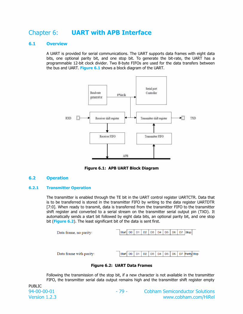
PUBLIC
94-00-00-01 - 79 - Cobham Semiconductor Solutions Version 1.2.3 www.cobham.com/HiRel
UART with APB Interface Chapter 6:
6.1 Overview
A UART is provided for serial communications. The UART supports data frames with eight data bits, one optional parity bit, and one stop bit. To generate the bit-rate, the UART has a
programmable 12-bit clock divider. Two 8-byte FIFOs are used for the data transfers between
the bus and UART. Figure 6.1 shows a block diagram of the UART.
Figure 6.1: APB UART Block Diagram
6.2 Operation
Transmitter Operation 6.2.1
The transmitter is enabled through the TE bit in the UART control register UARTCTR. Data that
is to be transferred is stored in the transmitter FIFO by writing to the data register UARTDTR
[7:0]. When ready to transmit, data is transferred from the transmitter FIFO to the transmitter shift register and converted to a serial stream on the transmitter serial output pin (TXD). It
automatically sends a start bit followed by eight data bits, an optional parity bit, and one stop bit (Figure 6.2). The least significant bit of the data is sent first.
Figure 6.2: UART Data Frames
Following the transmission of the stop bit, if a new character is not available in the transmitter
FIFO, the transmitter serial data output remains high and the transmitter shift register empty

PUBLIC
94-00-00-01 - 80 - Cobham Semiconductor Solutions Version 1.2.3 www.cobham.com/HiRel
bit (TS) is set in the UART status register. Transmission resumes and the TS is cleared when a
new character is loaded into the transmitter FIFO. When the FIFO is empty, the TE bit is set in the status register UARTSTR. If the transmitter is disabled, it immediately stops any active
transmissions including the character currently being shifted out from the transmitter shift register. The transmitter holding register may not be loaded when the transmitter is disabled or
when the transmitter FIFO is full. If this is done, data might be overwritten and one or more
frames lost.
The TF status bit (not to be confused with the TF control bit) is set if the transmitter FIFO is currently full and the TH bit is set as long as the FIFO is less than half-full, i.e. less than half of
entries in the FIFO contain data. The TF control bit in the control register UARTCTR enables FIFO interrupts when set. The status register also contains a counter (TCNT) showing the
current number of data entries in the transmitter FIFO.
Receiver Operation 6.2.2
The receiver is enabled for data reception through the receiver enable (RE) bit in the UART
control register. The receiver looks for a high to low transition of a start bit on the receiver serial
data input pin. If a transition is detected, the state of the serial input is sampled a half bit clock later. If the serial input is sampled high, the start bit is invalid and the search for a valid start
bit continues. If the serial input is still low, a valid start bit is assumed and the receiver continues to sample the serial input at one bit time intervals (at the theoretical center of the bit)
until the proper number of data bits and the parity bit have been assembled and one stop bit has been detected. The serial input is shifted through an 8-bit shift register where all bits need
the same value before the new value is taken into account, effectively forming a low-pass filter
with a cut-off frequency of 1/8 system clock.
The receiver also has a 8-byte receiver FIFO identical to the transmitter. FIFO data from the receiver FIFO is removed by reading the data register UARTDTR [7:0].
During reception, the least significant bit is received first. The data is then transferred to the receiver FIFO and the data ready (DR) bit is set in the UART status register as soon as the FIFO
contains at least one data frame. The parity, framing and overrun error bits are set at the received byte boundary at the same time as the receiver ready bit is set. The data frame is not
stored in the FIFO if an error is detected. Also, the new error status bits are OR’d with the old
values before they are stored into the status register. Thus, they are not cleared until written to with zeros from the APB bus. If both the receiver FIFO and shift registers are full when a new
start bit is detected, then the character held in the receiver shift register is lost and the overrun bit is set in the UART status register.
The RF status bit (not to be confused with the RF control bit) is set when the receiver FIFO is
full. The RH status bit is set when the receiver FIFO is half-full (at least half of the entries in the
FIFO contain data frames). The RF control bit in the control register UARTCTR enables receiver FIFO interrupts when set. A RCNT field is also available showing the current number of data
frames in the FIFO.
6.3 Baud Rate Generation Each UART contains a 12-bit down-counting scalar to generate the desired baud-rate. The
scalar is clocked by the system clock and generates a UART tick each time it underflows. It is reloaded with the value of the UART scalar reload register after each underflow. The resulting
UART tick frequency should be eight times the desired baud-rate.
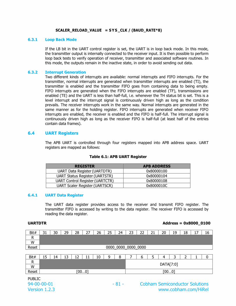
PUBLIC
94-00-00-01 - 81 - Cobham Semiconductor Solutions Version 1.2.3 www.cobham.com/HiRel
SCALER_RELOAD_VALUE = S Y S _CLK / (BAUD_RATE*8)
Loop Back Mode 6.3.1
If the LB bit in the UART control register is set, the UART is in loop back mode. In this mode,
the transmitter output is internally connected to the receiver input. It is then possible to perform
loop back tests to verify operation of receiver, transmitter and associated software routines. In this mode, the outputs remain in the inactive state, in order to avoid sending out data.
Interrupt Generation 6.3.2
Two different kinds of interrupts are available: normal interrupts and FIFO interrupts. For the transmitter, normal interrupts are generated when transmitter interrupts are enabled (TI), the
transmitter is enabled and the transmitter FIFO goes from containing data to being empty.
FIFO interrupts are generated when the FIFO interrupts are enabled (TF), transmissions are enabled (TE) and the UART is less than half-full, i.e. whenever the TH status bit is set. This is a
level interrupt and the interrupt signal is continuously driven high as long as the condition prevails. The receiver interrupts work in the same way. Normal interrupts are generated in the
same manner as for the holding register. FIFO interrupts are generated when receiver FIFO
interrupts are enabled, the receiver is enabled and the FIFO is half-full. The interrupt signal is continuously driven high as long as the receiver FIFO is half-full (at least half of the entries
contain data frames).
6.4 UART Registers The APB UART is controlled through four registers mapped into APB address space. UART
registers are mapped as follows:
Table 6.1: APB UART Register
REGISTER APB ADDRESS
UART Data Register (UARTDTR) 0x80000100
UART Status Register (UARTSTR) 0x80000104
UART Control Register (UARTCTR) 0x80000108
UART Scaler Register (UARTSCR) 0x8000010C
UART Data Register 6.4.1
The UART data register provides access to the receiver and transmit FIFO register. The transmitter FIFO is accessed by writing to the data register. The receiver FIFO is accessed by
reading the data register.
UARTDTR Address = 0x8000_0100
Bit# 31 30 29 28 27 26 25 24 23 22 21 20 19 18 17 16
R
W
Reset 0000_0000_0000_0000
Bit# 15 14 13 12 11 10 9 8 7 6 5 4 3 2 1 0
R DATA[7:0]
W
Reset [00…0] [00…0]

PUBLIC
94-00-00-01 - 82 - Cobham Semiconductor Solutions Version 1.2.3 www.cobham.com/HiRel
Figure 6.3: UART Data Register
Table 6.2: Description of UART Data Register
BIT NUMBER(S)
BIT NAME RESET STATE
DESCRIPTION
31-8 RESERVED [00...0]
7-0 DATA [00...0] Reading the data register accesses the receiver FIFO.
Writing to the data register access the transmitter FIFO.
UART Status Register 6.4.2
The UART Status Register provides information about the state of the FIFO’s and error
conditions.
UARTSTR Address = 0x8000_0104
Bit# 31 30 29 28 27 26 25 24 23 22 21 20 19 18 17 16
R RCNT[5:0] TCNT[5:0]
W
Reset [00…0] [00…0] [00…0]
Bit# 15 14 13 12 11 10 9 8 7 6 5 4 3 2 1 0
R
RF TF RH TH FE PE OV BR TE TS DR
W
Reset [00…0] 0 0 0 0 0 0 0 0 1 1 0
Figure 6.4: UART Status Register
Table 6.3: Description of UART Status Register
BIT
NUMBER(S) BIT NAME
RESET
STATE DESCRIPTION
31-26 RCNT [00...0] Receiver FIFO Count
Shows the number of data frames in the Receiver FIFO.
25-20 TCNT [00...0] Transmitter FIFO Count Shows the number of data frames in the Transmitter FIFO.
19-11 RESERVED [00...0] 10 RF 0 Receiver FIFO Full
Indicates that the Receiver FIFO is full.
9 TF 0 Transmitter FIFO Full
Indicates that the Transmitter FIFO is full.
8 RH 0 Receiver FIFO Half Full Indicates that at least half of the FIFO is holding data.
7 TH 0 Transmitter FIFO Half Full Indicates that the FIFO is less than half-full.
6 FE 0 Framing Error
Indicates that a framing error was detected.
5 PE 0 Parity Error Indicates that a parity error was detected.
4 OV 0 Overrun

PUBLIC
94-00-00-01 - 83 - Cobham Semiconductor Solutions Version 1.2.3 www.cobham.com/HiRel
BIT
NUMBER(S) BIT NAME
RESET
STATE DESCRIPTION
Indicates that one or more characters have been lost due to overrun.
3 BR 0 Break Received Indicates that a BREAK has been received.
2 TE 1 Transmitter FIFO Empty
Indicates that the transmitter FIFO is empty.
1 TS 1 Transmitter Shift Register Empty Indicates that the transmitter shift register is empty.
0 DR 0 Data Ready Indicates that new data is available in the receiver holding
register.
UART Control Register 6.4.3
The UART Control Register is used to enable the transmitter and receiver and control how interrupts are generated.
UARTCTR Address = 0x8000_0108
Bit# 31 30 29 28 27 26 25 24 23 22 21 20 19 18 17 16
R FA
W
Reset - [00…0]
Bit# 15 14 13 12 11 10 9 8 7 6 5 4 3 2 1 0
R SI DI BI RF TF EC LB FL PE PS TI RI TE RE
W
Reset 0 0 - - 0 0 0 - 0 - 0 0 0 0 - 0
Figure 6.5: UART Control Register
Table 6.4: Description of UART Control Register
BIT NUMBER(S)
BIT NAME RESET STATE
DESCRIPTION
31 FA - FIFOs available 0: only holding register are available. Read only
1: when receiver and transmitter FIFOs are available
30-15 RESERVED [00...0] 14 SI 0 Transmitter shift register empty interrupt enable
0: disabled
1: an interrupt will be generated when the transmitter shift register becomes empty
13 DI - Delayed interrupt enable
0: disabled 1: delayed receiver interrupts will be enabled and an
interrupt will only be generated for received characters after a delay of 4 character times + 4 bits if no new character has
been received during that interval. This is only applicable if
receiver interrupt enable is set

PUBLIC
94-00-00-01 - 84 - Cobham Semiconductor Solutions Version 1.2.3 www.cobham.com/HiRel
BIT
NUMBER(S) BIT NAME
RESET
STATE DESCRIPTION
12 BI - Break interrupt enable 0: disabled
1: an interrupt will be generated each time a break character is received
11 BD - FIFO debug mode enable
0: disabled 1: it is possible to read and write the FIFO debug register
10 RF 0 Receiver FIFO Interrupt Enable
0: Receiver FIFO level interrupts disabled 1: Receiver FIFO level interrupts enabled
9 TF 0 Transmitter FIFO Interrupt Enable 0: Transmitter FIFO level interrupts disabled
1: Transmitter FIFO level interrupts enabled
8 EC 0 External Clock (EC) 0: the UART scaler will be clocked by SYSCLK
1: the UART scaler will be clocked by UARTI.EXTCLK 7 LB 0 Loopback Mode 0: Disabled
1: Enabled
6 FL 0 Flow control (FL) control using CTS/RTS
0: Disabled 1: Enabled
5 PE 0 Parity Enable
0: Parity generation and checking disabled 1: Parity generation and checking enabled
4 PS 0 Parity Select 0: Even parity
1: Odd parity
3 TI 0 Transmitter Interrupt Enable 0: No frame interrupts
1: Interrupts generated when a frame is transmitted
2 RI 0 Receiver Interrupt Enable 0: No frame interrupts
1: Interrupts generated when a frame is received
1 TE 0 Transmitter Enable 0: Transmitter disabled
1: Transmitter enabled
0 RE 0 Receiver Enable 0: Receiver disabled
1: Receiver enabled
UART Scaler Register 6.4.4
UARTSCR Address = 0x8000_010C
Bit# 31 30 29 28 27 26 25 24 23 22 21 20 19 18 17 16
R
W
Reset [--…-]

PUBLIC
94-00-00-01 - 85 - Cobham Semiconductor Solutions Version 1.2.3 www.cobham.com/HiRel
Bit# 15 14 13 12 11 10 9 8 7 6 5 4 3 2 1 0
R SRV[11:0]
W
Reset 0000 [00…0]
Figure 6.6: UART Scalar Register
Table 6.5: Description of UART Scalar Register
BIT
NUMBER(S) BIT NAME
RESET
STATE DESCRIPTION
31-12 RESERVED [00...0] 11-0 SRV [00…0] Scaler Reload Value
SRV=SYS_CLK / (BAUD_RATE*8)

PUBLIC
94-00-00-01 - 86 - Cobham Semiconductor Solutions Version 1.2.3 www.cobham.com/HiRel
Timer Unit Chapter 7:
7.1 Overview
The Timer Unit implements a 12-bit prescaler and four 32-bit decrementing timers. The timer unit registers are accessed through the APB bus. The unit is capable of asserting an interrupt
when a timer underflows. A separate interrupt is available for each timer.
Figure 7.1: Timer Unit Block Diagram
7.2 Operation
The prescaler is clocked by the system clock and decremented on each clock cycle. When the
prescaler underflows, it is reloaded from the prescaler reload register and a timer tick is generated. Timers share the decrementer to save area. On the next timer tick, timer n+1 next
timer is decremented giving an effective division rate equal to SCALER_RELOAD_VALUE+1.
The operation of each timer is controlled through its control register. A timer is enabled by setting the enable bit (EN) in the control register. The timer value is then decremented on each
prescaler tick. When a timer underflows, it will automatically reloads with the value from the
corresponding timer reload register; if the restart bit (RS) in the control register is set, otherwise it stops at -1 and reset the enable bit.
Each timer signals its interrupt when the timer underflows (if the interrupt enable bit (IE) for
the current timer is set). The interrupt pending bit (IP) in the control register of the underflow
timer sets and remains set until cleared by writing ‘1’. Timer 1 generates interrupt 6, timer 2 generates interrupt 7, timer 3 generates interrupt 8, and timer 4 generates interrupt 9.
To minimize complexity, timers share the same decrementer. This means that the minimum allowed prescaler division factor is 5 (SCALER_RELOAD_VALUE=4).
By setting the chain bit (CH) in the control register timer n can be chained with preceding timer
n-1. Timer n will decrement each time when timer n-1 underflows.

PUBLIC
94-00-00-01 - 87 - Cobham Semiconductor Solutions Version 1.2.3 www.cobham.com/HiRel
Each timer can be reloaded with the value in its reload register at any time by writing a ‘1’ to
the load bit (LD) in the control register. Timer 4 also operates as a watchdog, driving the
watchdog output signal (WDOG) low when Timer 4 interrupt pending bit is set. The interrupt
pending bit is only set when interrupt is enable for the timer.
7.3 Registers Table 7.1 shows the timer unit registers.
Table 7.1: General Purpose Timer Unit Register
REGISTER APB ADDRESS
Scaler Value 0x80000300
Scaler Reload Value 0x80000304
Configuration Register 0x80000308
Timer 1 Counter Value Register 0x80000310
Timer 1 Reload Value Register 0x80000314
Timer 1 Control Register 0x80000318
Timer 2 Counter Value Register 0x80000320
Timer 2 Reload Value Register 0x80000324
Timer 2 Control Register 0x80000328
Timer 3 Counter Value Register 0x80000330
Timer 3 Reload Value Register 0x80000334
Timer 3 Control Register 0x80000338
Timer 4 Counter Value Register 0x80000340
Timer 4 Reload Value Register 0x80000344
Timer 4 Control Register 0x80000348
Figure 7.2 and Figure 7.3 show the layout of the timer unit registers
TIMSVR Address = 0x8000_0300
Bit# 31 30 29 28 27 26 25 24 23 22 21 20 19 18 17 16
R
W
Reset [11…1]
Bit# 15 14 13 12 11 10 9 8 7 6 5 4 3 2 1 0
R SCALER_VALUE[11:0]
W
Reset -- [11…1]
Figure 7.2: Scalar Value Register
TIMSRVR Address = 0x8000_0304
Bit# 31 30 29 28 27 26 25 24 23 22 21 20 19 18 17 16
R
W
Reset [11…1]

PUBLIC
94-00-00-01 - 88 - Cobham Semiconductor Solutions Version 1.2.3 www.cobham.com/HiRel
Bit# 15 14 13 12 11 10 9 8 7 6 5 4 3 2 1 0
R SCALER_RELOAD_VALUE[11:0]
W
Reset -- [11…1]
Figure 7.3: Scaler Reload Value Register
TIMTCR Address = 0x8000_0308
Bit# 31 30 29 28 27 26 25 24 23 22 21 20 19 18 17 16
R
W
Reset [00…0]
Bit# 15 14 13 12 11 10 9 8 7 6 5 4 3 2 1 0
R DF
SI IRQ[4:0] TIMERS
W
Reset [00…0] 0 1 0_0110 100
Figure 7.4: Timer Configuration Register
Table 7.2: Description of Timer Configuration Register
BIT
NUMBER(S) BIT NAME
RESET
STATE DESCRIPTION
31-10 RESERVED [00...0] 9 DF 0 Disable Timer Freeze
0: Timer unit can be frozen during debug mode
1: Timer unit cannot be frozen during debug mode
8 SI 1 Separate Interrupts
0: Single interrupt for timers
1: Each timer generates a separate interrupt Read=1; Write=Don’t care
7-3 IRQ 00110 APB Interrupt If configured for common interrupt, all timers drive APB
interrupt nr IRQ, otherwise timer n will drive APB Interrupt 4
+ n.
2-0 TIMERS 100 Number of Implemented Timers Read=100b; Write=Don’t
care
TIMCVR1
TIMCVR2 TIMCVR3
TIMCVR4
Address = 0x8000_0310
Address = 0x8000_0320 Address = 0x8000_0330
Address = 0x8000_0340
Bit# 31 30 29 28 27 26 25 24 23 22 21 20 19 18 17 16
R TIMER_COUNTER_VALUE[31:16]
W
Reset [--…-]

PUBLIC
94-00-00-01 - 89 - Cobham Semiconductor Solutions Version 1.2.3 www.cobham.com/HiRel
Bit# 15 14 13 12 11 10 9 8 7 6 5 4 3 2 1 0
R TIMER_COUNTER_VALUE[15:0]
W
Reset [--…-]
Figure 7.5: Timer Counter Value Register
Table 7.3: Description of Timer Counter Value Register
BIT
NUMBER(S) BIT NAME
RESET
STATE DESCRIPTION
31-0 Timer Counter Value
[--...-] Decremented by 1 for each tick, or when timer n- 1 underflows if in chain mode.
TIMRVR1 TIMRVR2
TIMRVR3 TIMRVR4
Address = 0x8000_0314 Address = 0x8000_0324
Address = 0x8000_0334 Address = 0x8000_0344
Bit# 31 30 29 28 27 26 25 24 23 22 21 20 19 18 17 16
R TIMER_RELOAD_VALUE[31:16]
W
Reset [--…-]
Bit# 15 14 13 12 11 10 9 8 7 6 5 4 3 2 1 0
R TIMER_RELOAD_VALUE[15:0]
W
Reset [--…-]
Figure 7.6: Timer Reload Value Register
Table 7.4: Description of Timer Reload Value Register
BIT NUMBER(S)
BIT NAME RESET STATE
DESCRIPTION
31-0 Timer Reload
Value
[--...-] This value is loaded into the timer counter value register when ‘1’ is written to bit LD in the timers control register,
or when the RS bit is set in the control register and the
timer underflows.
Note: Timer resets to value 0x000_FFFF
TIMCTR1
TIMCTR2 TIMCTR3
TIMCTR4
Address = 0x8000_0318
Address = 0x8000_0328 Address = 0x8000_0338
Address = 0x8000_0348
Bit# 31 30 29 28 27 26 25 24 23 22 21 20 19 18 17 16
R
W
Reset [00…0]

PUBLIC
94-00-00-01 - 90 - Cobham Semiconductor Solutions Version 1.2.3 www.cobham.com/HiRel
Bit# 15 14 13 12 11 10 9 8 7 6 5 4 3 2 1 0
R
DH CH IP IE LD RS EN
W
Reset [00…0] 0 0 0 1* 0 0 1*
Figure 7.7: Timer Control Register
Table 7.5: Description of Timer Control Register
BIT
NUMBER(S) BIT NAME
RESET
STATE DESCRIPTION
31-7 RESERVED [00...0] 6 DH 0 Debug Halt
State of timer when DF=0. Read only
0: Active 1: Frozen
5 CH 0 Chain with preceding timer
0: Timer functions independently 1: Timer n will decrement each time when timer n-1
underflows.
4 IP 0 Interrupt Pending 0: Interrupt not pending
1: Interrupt pending. Remains ‘1’ until cleared by writing ‘1’ to this bit
3 IE 1* Interrupt Enable (*see EN bit)
0: Interrupts disabled 1: Timer underflow signals interrupt
2 LD 0 Load Timer
Writing a ‘1’ to this bit loads the value from the timer reload register to the timer counter value register.
1 RS 0 Restart
Writing a ‘1’ to this bit reloads the timer counter value register with the value of the reload register when the timer
underflows.
0 EN 1* Timer Enable
*Timer 4 has reset value 0x9 (Watchdog timer is enable on
reset) *Timers 1 to 3 have reset values 0.
0: Disable 1: Enable

PUBLIC
94-00-00-01 - 91 - Cobham Semiconductor Solutions Version 1.2.3 www.cobham.com/HiRel
General Purpose I/O Port Chapter 8:
8.1 Overview
A general purpose I/O port is provided using the GRGPIO core from GRLIB. The unit implements a 16-bit I/O port with interrupt support. Each bit in the port is individually set as an
input or output and can optionally generate an interrupt. For interrupt generation, the input can
be filtered for polarity and level/edge detection. The Figure 8.1 below shows a diagram for one I/O line.
Figure 8.1: General Purpose I/O Port Diagram
8.2 Operation
The I/O ports are implemented as bi-directional buffers with programmable output enable. The input from each buffer is synchronized by two flip-flops in series to remove potential meta-
stability. The synchronized values can be read out from the I/O port data register. The output enable is controlled by the I/O port direction register. A ‘1’ in a bit position enables the output
buffer for the corresponding I/O line. The output value driven is taken from the I/O port output
register.
I/O ports 1-15 drive a separate interrupt line on the APB interrupt bus. The interrupt number is equal to the I/O line index (PIO[1] = interrupt 1, etc.). The interrupt generation is controlled by
three registers: interrupt mask, polarity and edge registers. To enable an interrupt, the corresponding bit in the interrupt mask register must be set. If the edge register is ‘0’, the
interrupt is treated as level sensitive. If the polarity register is ‘0’, the interrupt is active low. If
the polarity register is ‘1’, the interrupt is active high. If the edge register is ‘1’, the interrupt is edge-triggered. The polarity register then selects between rising edge (‘1’) or falling edge (‘0’).
8.3 Register
Table 8.1 shows the I/O port register addresses.
Table 8.1: I/O Port Registers
REGISTER APB ADDRESS
GPIO Port Data Register (GPIODVR) 0x80000900
GPIO Port Output Register (GPIODOR) 0x80000904
GPIO Port Direction Register (GPIODDR) 0x80000908
Interrupt Mask Register (GPIOIMR) 0x8000090C

PUBLIC
94-00-00-01 - 92 - Cobham Semiconductor Solutions Version 1.2.3 www.cobham.com/HiRel
REGISTER APB ADDRESS
Interrupt Polarity Register (GPIOIPR) 0x80000910
Interrupt Edge Register (GPIOIER) 0x80000914
GPIO Port Input Value Register 8.3.1
GPIODVR Address = 0x8000_0900
Bit# 31 30 29 28 27 26 25 24 23 22 21 20 19 18 17 16
R
W
Reset [00…0]
Bit# 15 14 13 12 11 10 9 8 7 6 5 4 3 2 1 0
R PORTVAL[15:0]
W
Reset [00…0]
Figure 8.2: GPIO Port Value Register
Table 8.2: Description of GPIO Port Value Register
BIT NUMBER(S)
BIT NAME RESET STATE
DESCRIPTION
31-16 RESERVED [00...0] 15-0 PORTVAL [00...0] GPIO Port Value
This read-only register indicates the state of port pin n.
0: Data=‘0’ 1: Data=‘1’
GPIO Port Data Output Register 8.3.2
GPIODOR Address = 0x8000_0904
Bit# 31 30 29 28 27 26 25 24 23 22 21 20 19 18 17 16
R
W
Reset [00…0]
Bit# 15 14 13 12 11 10 9 8 7 6 5 4 3 2 1 0
R
W PORTOUT[15:0]
Reset [00…0]
Figure 8.3: GPIO Port Data Register
Table 8.3: Description of GPIO Port Data Register
BIT
NUMBER(S) BIT NAME
RESET
STATE DESCRIPTION
31-16 RESERVED [00...0]

PUBLIC
94-00-00-01 - 93 - Cobham Semiconductor Solutions Version 1.2.3 www.cobham.com/HiRel
BIT
NUMBER(S) BIT NAME
RESET
STATE DESCRIPTION
15-0 PORTOUT [00...0] GPIO Port Data The port output register sets the state of port pin n when configured as an output. 0: Data=‘0’
1: Data=‘1’
GPIO Port Data Direction Register 8.3.3
GPIODDR Address = 0x8000_0908
Bit# 31 30 29 28 27 26 25 24 23 22 21 20 19 18 17 16
R
W
Reset [00…0]
Bit# 15 14 13 12 11 10 9 8 7 6 5 4 3 2 1 0
R PORTDDR[15:0]
W
Reset [00…0]
Figure 8.4: GPIO Port Data Direction Register
Table 8.4: Description of GPIO Port Data Direction Register
BIT NUMBER(S)
BIT NAME RESET STATE
DESCRIPTION
31-16 RESERVED [00...0] 15-0 PORTDDR [00...0] GPIO Data Direction
0: Port pin n configured as input
1: Port pin n configured as output
GPIO Interrupt Mask Register 8.3.4
GPIOIMR Address = 0x8000_090C
Bit# 31 30 29 28 27 26 25 24 23 22 21 20 19 18 17 16
R
W
Reset [00…0]
Bit# 15 14 13 12 11 10 9 8 7 6 5 4 3 2 1 0
R GPIOIMR[15:0]
W
Reset [00…0]
Figure 8.5: GPIO Interrupt Mask Register

PUBLIC
94-00-00-01 - 94 - Cobham Semiconductor Solutions Version 1.2.3 www.cobham.com/HiRel
Table 8.5: Description of GPIO Interrupt Mask Register
BIT
NUMBER(S) BIT NAME
RESET
STATE DESCRIPTION
31-16 RESERVED [00...0] 15-0 PORTDDR [00...0] GPIO Mask Register
0: Interrupt n disabled
1: Interrupt n enabled
GPIO Interrupt Priority Register 8.3.5
GPIOIPR Address = 0x8000_0910
Bit# 31 30 29 28 27 26 25 24 23 22 21 20 19 18 17 16
R
W
Reset [00…0]
Bit# 15 14 13 12 11 10 9 8 7 6 5 4 3 2 1 0
R GPIOIPR[15:0]
W
Reset [00…0]
Figure 8.6: GPIO Interrupt Mask Register
Table 8.6: Description of GPIO Interrupt Mask Register
BIT
NUMBER(S) BIT NAME
RESET
STATE DESCRIPTION
31-16 RESERVED [00...0] 15-0 GPIOIPR [00...0] GPIO Polarity Register
This register configures the polarity of interrupt n.
GPIOIER[n]=0 0: Active low
1: Active high GPIOIER[n]=1
0: Falling edge 1: Rising edge
GPIO Interrupt Edge Register 8.3.6
GPIOIER Address = 0x8000_0914
Bit# 31 30 29 28 27 26 25 24 23 22 21 20 19 18 17 16
R
W
Reset [00…0]
Bit# 15 14 13 12 11 10 9 8 7 6 5 4 3 2 1 0
R GPIOIER[15:0]
W
Reset [00...0]

PUBLIC
94-00-00-01 - 95 - Cobham Semiconductor Solutions Version 1.2.3 www.cobham.com/HiRel
Figure 8.7: GPIO Interrupt Edge Register
Table 8.7: Description of GPIO Interrupt Edge Register
BIT NUMBER(S)
BIT NAME RESET STATE
DESCRIPTION
31-16 RESERVED [00...0] 15-0 GPIOIER [00...0] GPIO Interrupt Edge Register
This register configures how an interrupt on port pin n is triggered. 0: Level triggered
1: Edge triggered

PUBLIC
94-00-00-01 - 96 - Cobham Semiconductor Solutions Version 1.2.3 www.cobham.com/HiRel
PCI Master/Target Unit Chapter 9:
9.1 Overview
The PCI Target/Master Unit is a bridge between the PCI bus and the AMBA AHB bus. The unit is connected to the PCI bus through the PCI Target interface and PCI Master Interface. The
AHB Slave and AHB Master interfaces connect the PCI core to the AHB bus. The PCI
Configuration and Status registers are accessed via the APB bus.
The PCI and AMBA interfaces belong to two different clock domains. Synchronization is performed inside the core through FIFOs.
Figure 9.1: PCI Master/Target Unit
9.2 Operation
PCI Target Unit 9.2.1
The PCI target interface and AHB master provide a connection between the PCI bus and the AHB bus. The PCI target is capable of handling configuration and single or burst memory cycles
on the PCI bus. Configuration cycles are used to access the Configuration Space Header of the
target, while the memory cycles are translated to AHB accesses. The PCI target interface can be programmed to occupy two areas in the PCI address space via registers BAR0 and BAR1
(Section 9.4). Mapping to the AHB address space is defined by map registers PAGE0 and PAGE1, which are accessible from PCI and AHB address space, respectively.
PCI Master Unit 9.2.2
The PCI master interface occupies one 1GB AHB memory bank and one 128 KB AHB I/O bank. Accesses to the memory area are translated to PCI memory cycles and accesses to the I/O area
generate I/O or configuration cycles. Generation of PCI cycles and mapping to the PCI address spaces is controlled through the Configuration/Status Register and the I/O Map Register
(Section 9.9).

PUBLIC
94-00-00-01 - 97 - Cobham Semiconductor Solutions Version 1.2.3 www.cobham.com/HiRel
Burst Transactions 9.2.3
Both target and master interfaces are capable of burst transactions. Data is buffered internally
in FIFO.
Byte Twisting 9.2.4
As PCI is little endian and the AHB controller is big endian, byte twisting is performed on all
accesses to preserve the byte ordering as shown in Figure 9.2. Byte twisting can be enabled or disabled in the PAGE0 register (Section 9.5).
Because of byte twisting, byte accesses work correctly. However, 16- and 32-bit PCI accesses need to be byte twisted before being sent to the PCI core.
Note: Accesses between the AHB bus and PCI bus are twisted. Accesses to the configuration
space are not byte twisted.
Figure 9.2: GRPCI Byte Twisting
9.3 PCI Target Interface The PCI target interface occupies two memory areas in the PCI address space as defined by the
BAR0 and BAR1 registers in the Configuration Space Header. Register BAR0 maps to a PCI space of 1MB; register BAR1 maps to a PCI space of 64MB.
The PCI Target interface handles the following PCI commands:
Configuration Read/Write: Single access to the Configuration Space Header. No AHB
access is performed
Memory Read: If prefetching is enabled, the AHB master interface fetches a cache line.
Otherwise, a single AHB access is performed Memory Read Line: The unit prefetches data according to the value of the Cache Line Size
register
Memory Read Multiple: The unit performs maximum prefetching
Memory Write

PUBLIC
94-00-00-01 - 98 - Cobham Semiconductor Solutions Version 1.2.3 www.cobham.com/HiRel
Memory Write and Invalidate
The target interface supports incremental bursts for PCI memory cycles. The target interface can finish a PCI transaction with one of the following abnormal responses:
Retry: This response indicates that the master should perform the same request later,
as the target is temporarily busy. This response is always given at least one time for
read accesses, but can also occur for write accesses.
Disconnect with data: Indicates that the target can accept one more data transaction, but no more. This occurs if the master tries to read more data than the
target has prefetched.
Disconnect without data: Indicates that the target is unable to accept more data.
This occurs if the master tries to write more data than the target can buffer. Target-Abort: Indicates that the current access caused an internal error and that the
target will not be able to complete the access.
The AHB master interface of the target is capable of burst transactions. Burst transactions are
performed on the AHB when supported by the destination unit (AHB slave); otherwise, multiple
single access is performed. A PCI burst crossing a 1 KB address boundary will be performed as multiple AHB bursts by the AHB master interface. The AHB master interface inserts an idle-cycle
before requesting a new AHB burst to allow for re-arbitration of the AHB. AHB transactions with a ‘retry’ response are repeated by the AHB master until an ‘okay’ or ‘error’ response is received.
The ‘error’ response on AHB bus results in a Target-Abort response for the PCI memory read
cycle. In the case of a PCI memory write cycle, the AHB access will not finish with an error response since write data is posted to the destination unit. Instead, the WE bit will be set in the
Configuration/Status register (APB address 0x80000400).
9.4 PCI Target Configuration Space Header Registers
The registers implemented in the PCI Configuration Space Header are listed in Table 9.1 and
described in this section.
Table 9.1: Configuration Space Header Registers
REGISTER CONFIGURATION SPACE
HEADER ADDRESS OFFSET
Device ID & Vendor ID 0x00
Status & Command 0x04
Class Code & Revision ID 0x08
BIST, Header Type, Latency Timer, Cache Line Size 0x0C
BAR0 0x10
BAR1 0x14
Max_Lat, Min_GNT, Interrupt 0x3C
Device/Vendor Offset = 0x00
Bit# 31 30 29 28 27 26 25 24 23 22 21 20 19 18 17 16
R DEVICE_ID[15:0]
W
Reset 0x699

PUBLIC
94-00-00-01 - 99 - Cobham Semiconductor Solutions Version 1.2.3 www.cobham.com/HiRel
Bit# 15 14 13 12 11 10 9 8 7 6 5 4 3 2 1 0
R VENDOR_ID[15:0]
W
Reset 0x1AD0
Figure 9.3: Device ID and Vendor ID Register
Table 9.2: Description of Device ID and Vendor ID Register
BIT
NUMBER(S) BIT NAME
RESET
STATE DESCRIPTION
31-16 DEVICE_ID 0x699 Returns the value of Device ID. Read=0x0699; Write=don’t care
15-0 VENDOR_ID 0x1AD0 Returns the value of Vendor ID. Read=0x1AD0;
Write=don’t care
PCISTAT Offset = 0x04
Bit# 31 30 29 28 27 26 25 24 23 22 21 20 19 18 17 16
R DPE RMA RTA STA
DST[1:0] DPD
W
Reset 0 0 0 0 0 10 0 [00…0]
Bit# 15 14 13 12 11 10 9 8 7 6 5 4 3 2 1 0
R PER MIE BM MS
W
Reset [00…0] 0 0 0 0 0 0 0
Figure 9.4: Status and Command Register
Table 9.3: Description of Status and Command Register
BIT
NUMBER(S) BIT NAME
RESET
STATE DESCRIPTION
31 DPE 0 Detected Parity Error
0: No parity error detected 1: Parity error detected
30 RESERVED 0 29 RMA 0 Received Master Abort
Set by the PCI master interface when its transaction is
terminated with Master-Abort. 0: PCI master transaction terminated with no Master-Abort
1: PCI master transaction terminated with Master-Abort
28 RTA 0 Received Target Abort Set by the PCI master interface when its transaction is
terminated with Target-Abort. 0: PCI master transaction terminated with no Target-Abort
1: PCI master transaction terminated with Target-Abort
27 STA 0 Signaled Target Abort Set by the PCI target interface when the target terminates
transaction with Target-Abort.
0: PCI target terminated with no Target-Abort 1: PCI target terminated with Target-Abort

PUBLIC
94-00-00-01 - 100 - Cobham Semiconductor Solutions Version 1.2.3 www.cobham.com/HiRel
BIT
NUMBER(S) BIT NAME
RESET
STATE DESCRIPTION
26-25 DST 10 Device Select Timing Read=10b; Write=don’t care.
24 DPD 0 Data Parity Error Detected
0: No data parity error detected 1: Data parity error detected
23-7 RESERVED 0 6 PER 0 Parity Error Response
Controls units response on parity error
5 RESERVED 0 4 MIE 0 Memory Write and Invalidate Enable
Enables the PCI Master interface to generate Memory Write and Invalidate command.
0: Disabled 1: Enabled
3 RESERVED 0 2 BM 0 Bus Master
Enables the Master Interface to generate PCI cycles. 0: Disabled
1: Enabled
1 MS 0 Memory Space Allows the unit to respond to memory space accesses.
0: Disabled 1: Enabled
0 RESERVED 0
PCICLASS Offset = 0x08
Bit# 31 30 29 28 27 26 25 24 23 22 21 20 19 18 17 16
R CLASS_CODE[23:8]
W
Reset 0xB4
Bit# 15 14 13 12 11 10 9 8 7 6 5 4 3 2 1 0
R CLASS_CODE[7:0] REVISION_ID[7:0]
W
Reset [00…0] [00…0]
Figure 9.5: Class Code and Revision Register
Table 9.4: Description of Class Code and Revision Register
BIT NUMBER(S)
BIT NAME RESET STATE
DESCRIPTION
31-8 CLASS_CODE 0xB4000 Returns the value of Class Code. Read=0x0B4000;
Write=don’t care
7-0 REVISION_ID 0x00 Returns the value of Revision ID. Read=0x00; Write=don’t
care

PUBLIC
94-00-00-01 - 101 - Cobham Semiconductor Solutions Version 1.2.3 www.cobham.com/HiRel
PCIBHLC Offset = 0x0C
Bit# 31 30 29 28 27 26 25 24 23 22 21 20 19 18 17 16
R BIST[7:0] HEADER[7:0]
W
Reset [00…0] [00…0]
Bit# 15 14 13 12 11 10 9 8 7 6 5 4 3 2 1 0
R LTIM[7:0] CLS[7:0]
W
Reset [00…0] [00…0]
Figure 9.6: BIST, Header Type, Latency Timer and Cache Line Size Register
Table 9.5: Description of BIST, Header Type, Latency Timer and Cache Line Size Register
BIT
NUMBER(S) BIT NAME
RESET
STATE DESCRIPTION
31-24 BIST [00...0] Built-in Self-Test Not supported. Read=0x00; Write=don’t care
23-16 HEADER [00...0] Header Type Read=0x00; Write=don’t care
15-8 LTIM [00...0] Latency Timer
Maximum number of PCI clock cycles that the PCI bus master can own the bus.
7-0 CLS [00...0] System Cache Line Size
Defines the prefetch length for Memory Read and Memory Read Line commands.
PCIBAR0 Offset = 0x10
Bit# 31 30 29 28 27 26 25 24 23 22 21 20 19 18 17 16
R BASE_ADDRESS_0[10:0]
W
Reset [00…0] 0_0000
Bit# 15 14 13 12 11 10 9 8 7 6 5 4 3 2 1 0
R
PR TP[1:0] MS
W
Reset [00…0] 0 00 0
Figure 9.7: BAR0 Register
Table 9.6: Description of BAR0 Register
BIT NUMBER(S)
BIT NAME RESET STATE
DESCRIPTION
31-21 BASE_ADDRESS
_0
[00...0] PCI Target Interface Base Address 0
A memory area of 2MB is defined at memory location BASE_ADDRESS_0. PCI memory accesses to the lower
half of this area are translated to AHB accesses using
PAGE0 map register (Section 9.5).

PUBLIC
94-00-00-01 - 102 - Cobham Semiconductor Solutions Version 1.2.3 www.cobham.com/HiRel
BIT
NUMBER(S) BIT NAME
RESET
STATE DESCRIPTION
20-4 RESERVED [00...0] This field can be used to determine the memory requirement of the target by writing all ‘1s’ to the BAR0
register and reading back the value. The device returns ‘0s’ in unimplemented bits positions effectively defining
the requested memory area. Read=00...0b; Write=don’t care
3 PR 0 Prefetchable
Read=0; Write=don’t care
2-1 TP 00 Type Read=0; Write=don’t care
0 MS 0 Memory Space Indicator Read=0; Write=don’t care
PCIBAR1 Offset = 0x14
Bit# 31 30 29 28 27 26 25 24 23 22 21 20 19 18 17 16
R BASE_ADDRESS_1
W
Reset [00…0] [00…0]
Bit# 15 14 13 12 11 10 9 8 7 6 5 4 3 2 1 0
R
PR TP[1:0] MS
W
Reset [00…0] 0 00 0
Figure 9.8: BAR1 Register
Table 9.7: Description of BAR1 Register
BIT
NUMBER(S) BIT NAME
RESET
STATE DESCRIPTION
31-26 BASE_ADDRESS_1 [00...0] PCI Target Interface Base Address 1. A memory area of
64MB is defined at memory location
BASE_ADDRESS_1. PCI memory accesses to this memory space are translated to AHB accesses using
PAGE1 map register (Section 9.5).
25-4 RESERVED [00...0] This field can be used to determine the memory
requirement of the target by writing all ‘1s’ to the BAR1
register and reading back the value. The device returns ‘0s’ in unimplemented bits positions effectively defining
the requested memory area. Read=00...0b; write=don’t care.
3 PR 0 Prefetchable
Read=0; Write=don’t care.
2-1 TP 00 Type
Read=0; Write=don’t care.
0 MS 0 Memory Space Indicator Read=0; Write=don’t care.

PUBLIC
94-00-00-01 - 103 - Cobham Semiconductor Solutions Version 1.2.3 www.cobham.com/HiRel
PCIMM Offset = 0x3C
Bit# 31 30 29 28 27 26 25 24 23 22 21 20 19 18 17 16
R Max_LAT[7:0] Min_GNT[7:0]
W
Reset [00…0] 0x01
Bit# 15 14 13 12 11 10 9 8 7 6 5 4 3 2 1 0
R Interrupt_Pin[7:0] Interupt_Line[7:0]
W
Reset 0x01 [--…-]
Figure 9.9: Max_LAT, Min_GNT and Interrupt Settings Register
Table 9.8: Description of Max_LAT, Min_GNT and Interrupt Settings Register
BIT
NUMBER(S) BIT NAME
RESET
STATE DESCRIPTION
31-24 Max_LAT [00...0] Maximum Latency Read only
23-16 Min_GNT 0x01 Minimum Grant
Read=0x01; Write=don’t care.
15-8 Interrupt Pin 0x01 Interrupt Pin Read=0x01; Write=don’t care.
7-0 Interrupt Line [--...-] Interrupt Line
Write able register used by the operating system to store information about interrupt routing.
9.5 PCI Target Map Registers
PAGE0 and PAGE1 registers map PCI accesses to AHB address space. PAGE0 is accessed from PCI accesses. PAGE1 can be accessed from the APB.
Table 9.9: PCI Target Map Registers
REGISTER ADDRESS
PAGE0 First address in the upper half of PCI address space defined by BAR0 register (BAR0 + 0x100000). Accessible only from the PCI
address space.
PAGE1 APB address 0x80000410
PAGE0 Register 9.5.1
Register PAGE0 provides a memory mapping between the PCI address space defined by
register BAR0 and the AHB address space. PAGE0 is only accessible from a PCI memory access and its location in PCI address space depends upon the value of BAR0. BAR0 provides a
mapping of 2 MB between the PCI address space and the PCI target. Only the lower half of the BAR0 space is used. The upper half is unused except for the lowest word, which is the location
of the PAGE0 register. This means that the effective address space of BAR0 is 1 MB. Any PCI
access to the lower half of the BAR0 address space will map to the AHB address space as defined by PAGE0. The following code example shows how to determine the location of PAGE0
using a PCI memory access, and how to configure PAGE0 to provide a mapping between the PCI address space and the APB address space.

PUBLIC
94-00-00-01 - 104 - Cobham Semiconductor Solutions Version 1.2.3 www.cobham.com/HiRel
/* Read the address of BAR0 */ pci_read_config_dword (bus, slot, function, 0x10, &tmp) /* Determine the PCI address of PAGE0 */ addr_page0 = tmp + 0x100000; /* Set PAGE0 to point to start of the APB memory space */ *addr_page0 = (unsigned int *) 0x80000000;
In this example, if the address of BAR0 is 0xC0000000, then the address of PAGE0 will be 0xC0100000. A write to PCI address 0xC0000000 translates to an AHB memory access at
address 0x80000000.
PCIPAGE0 Address = 0x8000_0408
Bit# 31 30 29 28 27 26 25 24 23 22 21 20 19 18 17 16
R PAGE0_MAP[11:0]
W
Reset [00…0] 0000
Bit# 15 14 13 12 11 10 9 8 7 6 5 4 3 2 1 0
R BTEN
W
Reset [00…0] 1
Figure 9.10: PAGE0 Register
Table 9.10: Description of PAGE0 Register
BIT NUMBER(S)
BIT NAME RESET STATE
DESCRIPTION
31-20 PAGE0_MAP [00...0] Maps PCI accesses to the PCI BAR0 address space to the AHB address space. The AHB address is formed by
concatenating PAGE0_MAP with PCI address AD[19:0].
19-1 RESERVED [00...0] Read=0x0; write=don’t care
0 BTEN 1 Byte Twisting Enable May be altered only when bus mastering is disabled.
0: Disabled 1: Enabled
PAGE1 Register 9.5.2
Register PAGE1 provides a memory mapping between the PCI address space defined by register BAR1 and the AHB address space. PAGE1 is accessible directly from the APB bus (APB
address 0x80000410), or indirectly from a PCI memory access if PAGE0 is used to map PCI
accesses to the APB memory space. BAR1 provides a mapping of 64MB between the PCI address space and the PCI target. PAGE1 can therefore be used to map 64MB of the PCI address
space to an equivalent size in the AHB memory space.

PUBLIC
94-00-00-01 - 105 - Cobham Semiconductor Solutions Version 1.2.3 www.cobham.com/HiRel
PCIPAGE1 Address = 0x8000_0410
Bit# 31 30 29 28 27 26 25 24 23 22 21 20 19 18 17 16
R PAGE1_MAP[5:0]
W
Reset [00…0] [00…0]
Bit# 15 14 13 12 11 10 9 8 7 6 5 4 3 2 1 0
R
W
Reset [00…0]
Figure 9.11: PAGE1 Register
Table 9.11: Description of PAGE1 Register
BIT
NUMBER(S) BIT NAME
RESET
STATE DESCRIPTION
31-26 PAGE1_MAP [00...0] Maps PCI accesses to the PCI BAR1 address space to the AHB address space. The AHB address is formed by
concatenating PAGE1_MAP with PCI address AD[25:0].
25-0 RESERVED [00...0] Read=0x0; write=don’t care
9.6 PCI Master Interface
The PCI master interface occupies 1GB of AHB memory address space and 128 KB of AHB I/O
address space. The PCI master interface handles AHB accesses to its back-end AHB Slave interface and translates them to one of the following PCI cycles: PCI configuration cycle, PCI
memory cycle, or PCI I/O cycle.
Mapping of the PCI master’s AHB address space is configurable through the
Configuration/Status Register and I/O Map Register (Section 9.7).
PCI Configuration Cycles 9.6.1
Single PCI Configuration cycles are performed by accessing the upper 64 KB of AHB I/O address space allocated by the PCI master’s AHB slave starting at address 0xFFF0FFFF. Type 0
configuration cycles are supported. Figure 9.12 shows the configuration access format.
PCICC Address = 0xFFF0_FFFF
Bit# 31 30 29 28 27 26 25 24 23 22 21 20 19 18 17 16
R ACM[15:0]
W
Reset [00…0]
Bit# 15 14 13 12 11 10 9 8 7 6 5 4 3 2 1 0
R IDSEL[4:0] FUNC[2:0] REGISTER[5:0] TP[1:0]
W
Reset [00…0] 000 [00…0] 00
Figure 9.12: Mapping of AHB I/O Addresses to PCI Address for PCI Configuration Cycles

PUBLIC
94-00-00-01 - 106 - Cobham Semiconductor Solutions Version 1.2.3 www.cobham.com/HiRel
Table 9.12: Description of Mapping of AHB I/O Addresses to PCI Address for PCI
Configuration Cycles
BIT NUMBER(S)
BIT NAME RESET STATE
DESCRIPTION
31-16 ACM [00...0] AHB Configuration Register Mapping These bits must always be set to 0xFFF1
15-11 IDSEL [00...0] This field is decoded to drive the PCI IDSEL lines during
configuration cycles.
10-8 FUNC 000 This field selects the function on a multi-function device.
7-2 REGISTER [00...0] This field selects the DWORD register in the con-
figuration space.
1-0 TP 00 Must be driven to ‘00’ to generate a Type 0 configuration cycle.
PCI I/O Cycles 9.6.2
PCI I/O cycles are performed by accessing the lower 64 KB of the AHB I/O address space occupied by the master’s AHB slave interface are translated into PCI I/O cycles starting at
address 0xFFF00000. Mapping is determined by the IOMAP field of I/O Map Register. The
IOMAP field of the I/O Map Register maps memory accesses between the PCI master (AHB memory space) and the PCI memory space when performing PCI I/O cycles. The PCI address is
formed by concatenating IOMAP with AHB address 15:0. IOMAP provides the 16 most-significant bits of the PCI I/O cycle address.
PCI Memory Cycles 9.6.3
PCI memory cycles are performed by accessing the 1GB AHB address space occupied by the master’s AHB slave starting at address 0xC0000000. Mapping and PCI command generation are
configured by programming the Configuration/Status Register (APB address 0x80000400). Burst operation is supported for PCI memory cycles. The MMAP field of the Configuration/Status
Register maps memory accesses between the PCI master (AHB memory space) and the PCI
address space when performing PCI memory cycles. The PCI address is formed by concatenating MMAP with AHB address 29:0. MMAP provides the two most-significant bits of
the PCI memory cycle address. PCI commands generated by the master are directly dependent upon the AMBA transfer type and the value of Configuration/Status Register. The
Configuration/Status Register can be programmed to issue the following PCI commands: Memory Read, Memory Read Line, Memory Read Multiple, Memory Write, and Memory Write
and Invalidate. If an AHB burst access is made to the PCI master’s AHB memory space, it is
translated to burst PCI memory cycle. When the PCI master interface is busy performing the transaction on the PCI bus, its AHB slave interface will not be able to accept new requests. A
‘Retry’ response will be given to all accesses to its AHB slave interface. The requesting AHB master repeats its request until an ‘OK’ or ‘Error’ response is given by the PCI master’s AHB
slave interface.
Note: ‘RETRY’ responses on the PCI bus are not transparent and are automatically retried by
the master PCI interface until the transfer is either finished or aborted. For burst accesses, only linear-incremental mode is supported and is directly translated from AMBA commands. Byte
enables on the PCI bus are translated from the HSIZE control AHB signal and the AHB address
according to the Table 9.13 below.

PUBLIC
94-00-00-01 - 107 - Cobham Semiconductor Solutions Version 1.2.3 www.cobham.com/HiRel
Note: only WORD, HALF-WORD and BYTE values of HSIZE are valid.
Table 9.13: Byte Enable Generation
HSIZE PCI_AD[1:0] PCI_CBE[3:0]
00 (8 bit) 00 1110
00 (8 bit) 01 1101
00 (8 bit) 10 1011
00 (8 bit) 11 0111
01 (16 bit) 00 1100
01 (16 bit) 10 0011
10 (32 bit) 00 0000
9.7 PCI Host Operation
The PCI core provides a host input signal that must be asserted (active low) for PCI host
operation. If this signal is asserted, the bus master interface is automatically enabled and the Bus Master (BM) bit is set in the Status and Command Register. An asserted PCI host signal
also enables the PCI target to respond to configuration cycles when the IDSEL signals AD[31:11] are not asserted. This is done in order for the master to be able to configure its own
target. For designs intended to operate only as a host or peripheral, this signal can be tied low or
high in the design. For multi-purpose designs it should be connected to the appropriate PCI connector pin. The PCI Industrial Computers Manufacturers Group (PICMG) cPCI specification
specifies pin C2 on connector P2 for this purpose. The pin should have pull-up resistors as peripheral slots leave it unconnected. PCI interrupts are supported as inputs for PCI hosts.
Note: PCI arbiter is NOT affected by the PCI_HOST input.
9.8 Interrupt Support
When acting as a PCI host, the GRPCI core can take the four PCI interrupt lines as inputs and use them to forward an interrupt to the interrupt controller.
There is no built-in support in the PCI core to generate PCI interrupts. These should be
generated by the respective IP core and drive an open-drain pad connected to the correct PCI interrupt line.
Note: All single function PCI devices should drive PCI Interrupt A.
9.9 Registers
The core is programmed through registers mapped into APB address space.
Table 9.14: AMBA Register
REGISTER APB ADDRESS NOTE
Configuration/Status
Register
0x80000400 Read/write access from the APB bus
BAR0 Register 0x80000404 Read-only access from the APB bus
Read/write access from the PCI bus
PAGE0 Register 0x80000408 Read-only access from the APB bus Read/write access from the PCI bus

PUBLIC
94-00-00-01 - 108 - Cobham Semiconductor Solutions Version 1.2.3 www.cobham.com/HiRel
REGISTER APB ADDRESS NOTE
BAR1 Register 0x8000040C Read-only access from the APB bus
Read/write access from the PCI bus
PAGE1 Register 0x80000410 Read/write access from the APB bus
IO Map Register 0x80000414 Read/write access from the APB bus
Status & Command Register 0x80000418 Read-only access from the APB bus Read/write access from the PCI bus
Interrupt Enable & Pending 0x8000041C -
APBCONF Address = 0x8000_0400
Bit# 31 30 29 28 27 26 25 24 23 22 21 20 19 18 17 16
R MMAP[1:0]
LTIMER[7:0]
W
Reset 00 [00…0] [00…0]
Bit# 15 14 13 12 11 10 9 8 7 6 5 4 3 2 1 0
R WE SH BM MS WB RB
CTO CLS[7:0]
W
Reset 0 0 0 0 0 0 0 0 [00…0]
Figure 9.13: Configuration and Status Register
Table 9.15: Description of Configuration and Status Register (Read Only)
BIT
NUMBER(S) BIT NAME
RESET STATE
DESCRIPTION
31-30 MMAP 00 Memory Space Map Register
Maps memory accesses between the PCI master (AHB memory space) and PCI address space when performing
PCI memory cycles. The PCI address is formed by concatenating MMAP with AHB address 29:0
29-23 RESERVED [00...0] 22-15 LTIMER [00...0] Latency Timer (read only)
Value of Latency Timer in the Configuration Space Header.
14 WE 0 Target Write Error (read only) 0: No error
1: Write access to target interface resulted in error
13 SH 0 System Host (read only) 0: Unit is not system host
1: Unit is system host
12 BM 0 Bus Master (read only) Value of the Bus Master field in the Command register of
the Configuration Space Header
11 MS 0 Memory Space (read only) Value of Memory Space field in the Command register of
the Configuration Space Header
10 WB 0 Write Burst Command Defines the PCI command used for PCI write bursts.
0: Memory Write
PUBLIC
94-00-00-01 - 109 - Cobham Semiconductor Solutions Version 1.2.3 www.cobham.com/HiRel
BIT
NUMBER(S) BIT NAME
RESET
STATE DESCRIPTION
1: Memory Write and Invalidate
9 RB 0 Read Burst Command
Defines the PCI command used for PCI read bursts. 0: Memory Read Multiple
1: Memory Read Line
8 CTO 0 Configuration Timeout (read only) 0: No timeout occurred during configuration cycle
1: Timeout occurred during configuration cycle
7-0 CLS [00...0] Cache Line Size (read only) Value of Cache Line Size register in Configuration Space
Header.
APBBAR0 Address = 0x8000_0404
Bit# 31 30 29 28 27 26 25 24 23 22 21 20 19 18 17 16
R BASE_ADDRESS_0[10:0]
W
Reset [00…0] 0_0000
Bit# 15 14 13 12 11 10 9 8 7 6 5 4 3 2 1 0
R
PR TP[1:0] MS
W
Reset [00…0] 0 00 0
Figure 9.14: Configuration and Status Register
Table 9.16: Description of Configuration and Status Register (Read Only)
BIT
NUMBER(S) BIT NAME
RESET
STATE DESCRIPTION
31-21 BASE_ADDRESS_0 [00...0] PCI Target Interface Base Address 0 A memory area of 2MB is defined at memory location
BASE_AD- DRESS_0. PCI memory accesses to the lower
half of this area are translated to AHB accesses using PAGE0 map register (Section 9.5).
20-4 RESERVED [00...0] This field can be used to determine the memory requirement of the target by writing all ‘1s’ to the BAR0
register and reading back the value. The device returns
‘0s’ in unimplemented bits positions effectively defining the requested memory area.
Read=00...0b; write=don’t care
3 PR 0 Prefetchable Read=0; Write=don’t care
2-1 TP 0 Type Read=0; Write=don’t care
0 MS 00 Memory Space Indicator Read=0;
Write=don’t care

PUBLIC
94-00-00-01 - 110 - Cobham Semiconductor Solutions Version 1.2.3 www.cobham.com/HiRel
APBPAGE0 Address = 0x8000_0408
Bit# 31 30 29 28 27 26 25 24 23 22 21 20 19 18 17 16
R PAGE0_MAP[11:0]
W
Reset [00…0] 0000
Bit# 15 14 13 12 11 10 9 8 7 6 5 4 3 2 1 0
R BTEN
W
Reset [00…0] 1
Figure 9.15: PAGE0 Register
Table 9.17: Description of PAGE0 Register
BIT
NUMBER(S) BIT NAME
RESET
STATE DESCRIPTION
31-20 PAGE0_MAP [00...0] Maps PCI accesses to the PCI BAR0 address space to the AHB address space. The AHB address is formed by
concatenating PAGE0_MAP with PCI address AD[19:0].
19-1 RESERVED [00...0] Read=00...0b; write=don’t care
0 BTEN 1 Byte Twisting Enable
May be altered only when bus mastering is disabled. 0: Disabled
1: Enabled
APBBAR1 Address = 0x8000_040C
Bit# 31 30 29 28 27 26 25 24 23 22 21 20 19 18 17 16
R BASE_ADDRESS_1[5:0]
W
Reset [00…0] [00…0]
Bit# 15 14 13 12 11 10 9 8 7 6 5 4 3 2 1 0
R
PR TP[1:0] MS
W
Reset [00…0] 0 00 0
Figure 9.16: BAR1 Register
Table 9.18: Description of BAR1 Register (Read Only)
BIT NUMBER(S)
BIT NAME RESET STATE
DESCRIPTION
31-26 BASE_ADDRESS_1 [00...0] PCI Target Interface Base Address 1. A memory area of 64MB is defined at memory location BASE_ADDRESS_1.
PCI memory accesses to this memory space are
translated to AHB accesses using PAGE1 map register (Section 9.5).
25-4 RESERVED [00...0] This field can be used to determine the memory
requirement of the target by writing all ‘1s’ to the BAR1

PUBLIC
94-00-00-01 - 111 - Cobham Semiconductor Solutions Version 1.2.3 www.cobham.com/HiRel
BIT
NUMBER(S) BIT NAME
RESET
STATE DESCRIPTION
register and reading back the value. The device returns ‘0s’ in unimplemented bits positions effectively defining
the requested memory area. Read=00...0b; write=don’t care.
3 PR 0 Prefetchable
Read=0; Write=don’t care.
2-1 TP 00 Type
Read=0; Write=don’t care.
0 MS 0 Memory Space Indicator Read=0; Write=don’t care.
APBPAGE1 Address = 0x8000_0410
Bit# 31 30 29 28 27 26 25 24 23 22 21 20 19 18 17 16
R PAGE1_MAP[5:0]
W
Reset [00…0] [00…0]
Bit# 15 14 13 12 11 10 9 8 7 6 5 4 3 2 1 0
R
W
Reset [00…0]
Figure 9.17: PAGE1 Register
Table 9.19: Description of PAGE1 Register
BIT NUMBER(S)
BIT NAME RESET STATE
DESCRIPTION
31-26 PAGE1_MAP [00...0] Maps PCI accesses to the PCI BAR1 address space to the
AHB address space. The AHB address is formed by concatenating PAGE1_MAP with PCI address AD[25:0].
25-0 RESERVED [00...0] Read=00...0b; write=don’t care
APBIOM Address = 0x8000_0414
Bit# 31 30 29 28 27 26 25 24 23 22 21 20 19 18 17 16
R IOMAP[15:0]
W
Reset [00…0]
Bit# 15 14 13 12 11 10 9 8 7 6 5 4 3 2 1 0
R
W
Reset [00…0]
Figure 9.18: I/O Map Register

PUBLIC
94-00-00-01 - 112 - Cobham Semiconductor Solutions Version 1.2.3 www.cobham.com/HiRel
Table 9.20: Description of I/O Map Register (Read Only)
BIT
NUMBER(S) BIT NAME
RESET
STATE DESCRIPTION
31-16 IOMAP [00...0] Maps memory accesses between the PCI master (AHB memory space) and the PCI memory space when
performing PCI I/O cycles. The PCI address is formed by concatenating MMAP with AHB address 15:0.
15-0 RESERVED [00...0]
APBSTAT Address = 0x8000_0418
Bit# 31 30 29 28 27 26 25 24 23 22 21 20 19 18 17 16
R DPE
RMA RTA STA
DST[1:0] DPD
W
Reset 0 0 0 0 0 10 0 [00…0]
Bit# 15 14 13 12 11 10 9 8 7 6 5 4 3 2 1 0
R MIE BM MS
W
Reset [00…0] 0 0 0 0 0
Figure 9.19: Status and Command Register
Table 9.21: Description of Status and Command Register
BIT NUMBER(S)
BIT NAME RESET STATE
DESCRIPTION
31 DPE 0 Detected Parity Error
0: No parity error detected 1: Parity error detected
30 RESERVED 0 29 RMA 0 Received Master Abort
Set by the PCI master interface when its transaction is
terminated with Master-Abort.
0: PCI master transaction terminated with no Master-Abort
1: PCI master transaction terminated with Master-Abort
28 RTA 0 Received Target Abort Set by the PCI master interface when its transaction is
terminated with Target-Abort. 0: PCI master transaction terminated with no Target-
Abort 1: PCI master transaction terminated with Target-Abort
Clear by writing a "1" to this bit, otherwise this bit is read
only.
27 STA 0 Signaled Target Abort
Set by the PCI target interface when the target
terminates transaction with Target-Abort. 0: PCI target terminated with no Target-Abort
1: PCI target terminated with Target-Abort Clear by writing a "1" to this bit, otherwise this bit is read

PUBLIC
94-00-00-01 - 113 - Cobham Semiconductor Solutions Version 1.2.3 www.cobham.com/HiRel
BIT
NUMBER(S) BIT NAME
RESET
STATE DESCRIPTION
only.
26-25 DST 10 Device Select Timing Read=10b; Write=don’t care.
24 DPD 0 Data Parity Error Detected
0: No data parity error detected 1: Data parity error detected
Clear by writing a "1" to this bit, otherwise this bit is read only.
23-5 RESERVED [[00…0] 4 MIE 0 Memory Write and Invalidate Enable
Enables the PCI Master interface to generate Memory Write and Invalidate command.
0: Disabled 1: Enabled
3 RESERVED 0 2 BM 0 Bus Master
Enables the Master Interface to generate PCI cycles.
0: Disabled
1: Enabled
1 MS 0 Memory Space
Allows the unit to respond to memory space accesses. 0:
Disabled 1: Enabled
0 RESERVED 0
APBIPR Address = 0x8000_041C
Bit# 31 30 29 28 27 26 25 24 23 22 21 20 19 18 17 16
R ENABLE[9:0]
W
Reset [00…0] [00…0]
Bit# 15 14 13 12 11 10 9 8 7 6 5 4 3 2 1 0
R DPE SSE RMA RTA STA DPED A:D
W
Reset [00..0] 0 0 0 0 0 0 0000
Figure 9.20: Interrupt and Pending Register
Table 9.22: Description of Interrupt and Pending Register
BIT NUMBER(S)
BIT NAME RESET STATE
DESCRIPTION
31-26 RESERVED [00…0] 25-16 ENABLE [00…0] Interrupt Enable for bits [9.0]
15-10 RESERVED [00…0]
9 DPE 0 Detected Parity Error Interrupt
8 SSE 0 Signaled System Error Interrupt
7 RMA 0 Received Master Abort Interrupt
6 RTA 0 Received Target Abort Interrupt

PUBLIC
94-00-00-01 - 114 - Cobham Semiconductor Solutions Version 1.2.3 www.cobham.com/HiRel
BIT
NUMBER(S) BIT NAME
RESET
STATE DESCRIPTION
5 STA 0 Signaled Target Abort Interrupt
4 DPED 0 Data Parity Error Detected Interrupt
3-0 A:D 0000 PCI IRQ A-D Interrupt (host only)

PUBLIC
94-00-00-01 - 115 - Cobham Semiconductor Solutions Version 1.2.3 www.cobham.com/HiRel
DMA Controller for the GRPCI Interface Chapter 10:
10.1 Introduction
The DMA controller is an add-on interface to the GRPCI interface. This controller performs bursts to or from the PCI bus using the master interface of the PCI Target/Master unit.
Figure 10.1 illustrates how the DMA controller is attached between the AHB bus and the PCI master interface.
Figure 10.1: DMA Controller Unit
10.2 Operation The DMA controller is set up by defining the location of memory areas between which the DMA
interfaces to PCI and AHB address spaces, as well as the direction, length, and type of transfer. Only 32-bit word transfers are supported.
The DMA transfer is automatically aborted when any kind of error is detected during a transfer. In the event of an error, the ERR bit of the Status and Command Register is set. The DMA
controller does not detect deadlocks in its communication channels. If the system concludes that a deadlock has occurred, it manually aborts the DMA transfer. The DMA controller may
perform bursts over a 1 KB boundary of the AHB bus, which is the maximum data burst that may occur over the bus per AMBA specification. When the size of the data burst exceeds the 1
KB boundary, AHB idle cycles are automatically inserted to break up the burst over the
boundary.

PUBLIC
94-00-00-01 - 116 - Cobham Semiconductor Solutions Version 1.2.3 www.cobham.com/HiRel
When the DMA is not active, the AHB slave interface of PCI Target/Master unit directly connects
to AMBA AHB bus.
10.3 Registers
The core is programmed through registers mapped into APB address space.
Table 10.1: APB Address Register
Register APB Address
Command and Status Register (DMASCR) 0x80000500
AMBA Target Address Register (DMAATA) 0x80000504
PCI Target Address Register (DMAPTA) 0x80000508
Burst Length Register (DMALNR) 0x8000050C
DMASCR Address = 0x8000_0500
Bit# 31 30 29 28 27 26 25 24 23 22 21 20 19 18 17 16
R
W
Reset [00…0]
Bit# 15 14 13 12 11 10 9 8 7 6 5 4 3 2 1 0
R TTYPE[3:0] ERR RDY TD ST
W
Reset [00…0] 0000 0 0 0 0
Figure 10.2: Status and Command Register
Table 10.2: Description of Status and Command Register
BIT
NUMBER(S) BIT NAME
RESET
STATE DESCRIPTION
31-8 RESERVED [00...0] 7-4 TTYPE 0000 Transfer Type
Perform either PCI memory or I/O cycles 0100b: Perform I/O cycles
1000b: Perform memory cycles
3 ERR 0 Error Last transfer was abnormally terminated. If set by the
DMA controller, this bit remains one until cleared by writing ‘1’ to it.
2 RDY 0 Ready
Current transfer is completed. When set by the DMA Controller this bit remains one until cleared by writing ‘1’
to it.
1 TD 0 Transfer Direction 0: Read from PCI 1: Write to PCI
0 ST 0 Start DMA Transfer
Writing ‘1’ starts the DMA transfer. All other registers
must be configured before setting this bit. Set by the PCI Master interface when its transaction is terminated with
Target-Abort.

PUBLIC
94-00-00-01 - 117 - Cobham Semiconductor Solutions Version 1.2.3 www.cobham.com/HiRel
DMAATA Address = 0x8000_0504
Bit# 31 30 29 28 27 26 25 24 23 22 21 20 19 18 17 16
R ATA[31:16]
W
Reset 0x77FF
Bit# 15 14 13 12 11 10 9 8 7 6 5 4 3 2 1 0
R ATA[15:0]
W
Reset 0x9324
Figure 10.3: AMBA Target Address Register
Table 10.3: Description of AMBA Target Address Register
BIT NUMBER(S)
BIT NAME RESET STATE
DESCRIPTION
31-0 ATA 0x77FF9
324
AMBA Target Address
AHB start address for the data on the AMBA bus. In case of error, it indicates the failing address.
DMAPTA Address = 0x8000_0508
Bit# 31 30 29 28 27 26 25 24 23 22 21 20 19 18 17 16
R PTA[31:16]
W
Reset [00…0]
Bit# 15 14 13 12 11 10 9 8 7 6 5 4 3 2 1 0
R PTA[15:0]
W
Reset [00…0]
Figure 10.4: PCI Target Address Register
Table 10.4: Description of PCI Target Address Register
BIT NUMBER(S)
BIT NAME RESET STATE
DESCRIPTION
31-0 PTA [00...0] PCI Target Address
PCI start address on the PCI bus. This is a complete 32-bit PCI address and is not further mapped by the PCI Target/
Master unit. In case of error, it indicates the failing
address.

PUBLIC
94-00-00-01 - 118 - Cobham Semiconductor Solutions Version 1.2.3 www.cobham.com/HiRel
DMALNR Address = 0x8000_050C
Bit# 31 30 29 28 27 26 25 24 23 22 21 20 19 18 17 16
R
W
Reset [00…0]
Bit# 15 14 13 12 11 10 9 8 7 6 5 4 3 2 1 0
R LEN[11:0]
W
Reset 0000 0x933
Figure 10.5: Burst Length Register
Table 10.5: Description of Burst Length Register
BIT
NUMBER(S) BIT NAME
RESET
STATE DESCRIPTION
31-12 RESERVED [00...0] 11-0 LEN 0x933 Burst Length
Number of 32-bit words to be transferred.

PUBLIC
94-00-00-01 - 119 - Cobham Semiconductor Solutions Version 1.2.3 www.cobham.com/HiRel
PCI Arbiter, PCIARB Chapter 11:
11.1 Overview
PCIARB is an arbiter for the PCI bus according to the PCI specification version 2.1. It provides 8 REQ/GNT pairs for PCI masters. The arbiter uses nested round-robin policy in two priority levels.
The priority assignment is programmable through an APB interface.
11.2 Operation
Scheduling Algorithm 11.2.1
The arbiter uses the algorithm described in the implementation note of Section 3.4 of the PCI standard. The bus is granted by two nested round-robin loops, where an agent number and a
priority level is assigned to each agent. The agent number determines which pair of REQ/GNT lines is used. Agents are counted from 0 to 7. All agents in one level have equal access to the
bus through a round-robin policy. All agents of level 1 as a group have access equal to each agent of level 0. Re-arbitration occurs, when FRAMEN is asserted, as soon as any other master
as requested the bus, but only once per transaction.
The priority level of all agents except 7 is programmable via the priority register at address
0x80000880. Each bit indicates if the corresponding REQ/GNT pair is assigned to level 1 or 0. The reset value in registers is ‘1’. The arbiter is always enabled.
ARBPRI Address = 0x8000_0880
Bit# 31 30 29 28 27 26 25 24 23 22 21 20 19 18 17 16
R
W
Reset [--…-]
Bit# 15 14 13 12 11 10 9 8 7 6 5 4 3 2 1 0
R 1 PRI[6:0]
W
Reset [--…-] 1 [11…1]
Figure 11.1: Priority Register
Timeout 11.2.2
The “broken master” time-out is another reason for re-arbitration (Section 3.4.1 of the PCI standard). Grant is removed from an agent, which has not started a cycle within 16 cycles after
request (and grant). Reporting of such a ‘broken’ master is not implemented.
Turn-Around 11.2.3
A turn-around cycle is required by the standard, when re-arbitration occurs during idle state of the bus. The “idle state” is assumed when FRAMEN is high for more than 1 cycle.

PUBLIC
94-00-00-01 - 120 - Cobham Semiconductor Solutions Version 1.2.3 www.cobham.com/HiRel
Bus Parking 11.2.4
The bus is parked to agent 0 after reset, it remains granted to the last owner if no other agent
requests the bus. When another request is asserted, re-arbitration occurs after one turn-around cycle.
Lock 11.2.5
Lock is defined as a resource lock by the PCI standard. The optional bus lock mentioned in the standard is not considered here and there are no special conditions to handle when LOCKN is
active during arbitration.
Latency 11.2.6
Latency control in PCI is via the latency counters of each agent. The arbiter does not perform
any latency check and a once granted agent continues its transaction until its grant is removed AND its own latency counter has expired. Even though a bus re-arbitration occurs during a
transaction, the hand-over only becomes effective when the current owner deasserts
PCI_FRAME.

PUBLIC
94-00-00-01 - 121 - Cobham Semiconductor Solutions Version 1.2.3 www.cobham.com/HiRel
SpaceWire Interface with RMAP support Chapter 12:(GRSPW2)
12.1 Overview
The SpaceWire core provides an interface between the AHB bus and a SpaceWire network. It implements the SpaceWire standard (ECSS-E-ST-50-12C) with the protocol identification
extension (ECSS-E-ST-50-51C). The Remote Memory Access Protocol (RMAP) target implements the ECSS standard (ECSS-E-ST-50-52C).
The SpaceWire interface is configured through 11 hardware registers accessed through the APB interface. Data is transferred through DMA channels using an AHB master interface.
There are two clock domains for the four SpaceWire ports: (1) the system clock is utilized for
the AHB interface, (2) the transmitter clock (TxClk) and the receive sample clock comes from
the external SPW_CLK pin. For proper operation, the receiver data rate must be no more than eight times as fast as the system clock and the transmitter clock frequency must be no more
than eight times the system clock. The link frequency must be 10+1 MHz.
Figure 12.1: SpaceWire Block Diagram
12.2 Operation
Overview 12.2.1
The main sub-blocks of the GRSPW2 are the link interface, the RMAP target and the AMBA
interface. A block diagram of the internal structure can be found in Figure 12.1. The link interface consists of the receiver, transmitter and the link interface FSM. They handle
communication on the SpaceWire network. The AMBA interface consists of the DMA engines, the AHB master interface and the APB interface. The link interface provides FIFO interfaces to
the DMA engines. These FIFOs are used to transfer N-Chars between the AMBA and SpaceWire
domains during reception and transmission.

PUBLIC
94-00-00-01 - 122 - Cobham Semiconductor Solutions Version 1.2.3 www.cobham.com/HiRel
The RMAP target handles incoming packets which are determined to be RMAP commands
instead of the receiver DMA engine. The RMAP command is decoded and if it is valid, the operation is performed on the AHB bus. If a reply was requested it is automatically transmitted
back to the source by the RMAP transmitter. The GRSPW2 is controlled by writing to a set of user registers through the APB interface. The link interface, RXDMA engine, TXDMA engine,
RMAP target and AMBA interface are described in Sections 12.3, 12.4, 12.5, 12.6 and 12.7
respectively.
Protocol Support 12.2.2
The GRSPW2 only accepts packets with a valid destination address in the first received byte. Packets with address mismatch will be silently discarded (except in promiscuous mode which is
covered in Section 12.4.10). The second byte is sometimes interpreted as a protocol ID as
described hereafter. The RMAP protocol (ID=0x1) is the only protocol handled separately in hardware while other packets are stored to a DMA channel. The RMAP target will process,
execute and reply to all RMAP commands automatically controlled by hardware. Otherwise RMAP commands are stored to a DMA channel in the same way as other packets. RMAP replies
are always stored to a DMA channel.
More information on the RMAP protocol support is found in Section 12.6. RMAP is only utilized
when the RMAP protocol ID is included in a packet.
All packets arriving with the extended protocol ID (0x00) are stored to a DMA channel. This means that the hardware RMAP target will not work if the incoming RMAP packets use the
extended protocol ID. Note: Packets with the reserved extended protocol identifier (ID =
0x000000) are not ignored by the GRSPW2. It is up to the client receiving the packets to ignore them. When transmitting packets, the address and protocol-ID fields must be included in the
buffers from where data is fetched. They are not automatically added by the GRSPW2.
Figure 12.2 shows the packet types accepted by the GRSPW2. The GRSPW2 also allows
reception and transmission with extended protocol identifiers, but without support for RMAP CRC calculations and the RMAP target.
Figure 12.2: SpaceWire Packet Types Supported by the Core
12.3 Link Interface
The link interface handles the communication on the SpaceWire network and consists of a transmitter, receiver, a FSM and FIFO interfaces. An overview of the architecture is found in
Figure 12.1.
Link Interface FSM 12.3.1
The FSM controls the link interface (a more detailed description is found in the SpaceWire
standard). The low-level protocol handling (the signal and character level of the SpaceWire

PUBLIC
94-00-00-01 - 123 - Cobham Semiconductor Solutions Version 1.2.3 www.cobham.com/HiRel
standard) is handled by the transmitter and receiver while the exchange level is handled by the
FSM.
The link interface FSM is controlled through the control register. The link can be disabled through the link disable bit, which depending on the current state; either prevents the link
interface from reaching the started state or forces it to the error-reset state. When the link is
not disabled, the link interface FSM is allowed to enter the started state when either the link start bit is set or when a NULL character has been received and the auto-start bit is set.
The current state of the link interface determines which type of characters is allowed to be
transmitted together with the requests made from the host interface determines the character sent. Time-codes are sent when the FSM is in the run-state and a request is made through the
time-interface (described in Section 12.3.4).
When the link interface is in the connecting- or run-state, it is allowed to send FCTs. FCTs are
sent automatically by the link interface when possible. This is done based on the maximum value of 56 for the outstanding credit counter and the currently free space in the receiver N-
Char FIFO. FCTs are sent as long as the outstanding counter is less than or equal to 48 and
there are at least 8 more empty FIFO entries than the counter value. N-Chars are sent in the run-state when they are available from the transmitter FIFO and there are credits available.
NULLs are sent when no other character transmission is requested or the FSM is in a state where no other transmissions are allowed.
The credit counter (incoming credits) is automatically increased when FCTs are received and
decreased when N-Chars are transmitted. Received N-Chars are stored to the receiver N-Char
FIFO for further handling by the DMA interface. Received time-codes are handled by the time-interface.
Transmitter 12.3.2
The state of the FSM, credit counters, requests from the time-interface and requests from the DMA-interface are used to decide the next character to be transmitted. The type of character
and the character itself (for N-Chars and time-codes) to be transmitted are presented to the low-level transmitter which is located in a separate clock-domain.
This is done to run the SpaceWire link on a different frequency than the host system clock. The GRSPW2 has a separate clock input which is used to generate the transmitter clock. Since the
transmitter often runs on high frequency clocks (up to 200 MHz), as much logic as possible has been placed in the system clock domain to minimize power consumption and timing issues.
The transmitter logic in the host clock domain decides what character to send next and sets the proper control signal and presents any needed character to the low-level transmitter as
shown in Figure 12.3. The transmitter sends the requested characters and generates parity and control bits as needed. If no requests are made from the host domain, NULLs are sent as
long as the transmitter is enabled. Most of the signal and character levels of the SpaceWire standard are handled in the transmitter. External LVDS drivers are needed for the data and
strobe signals.
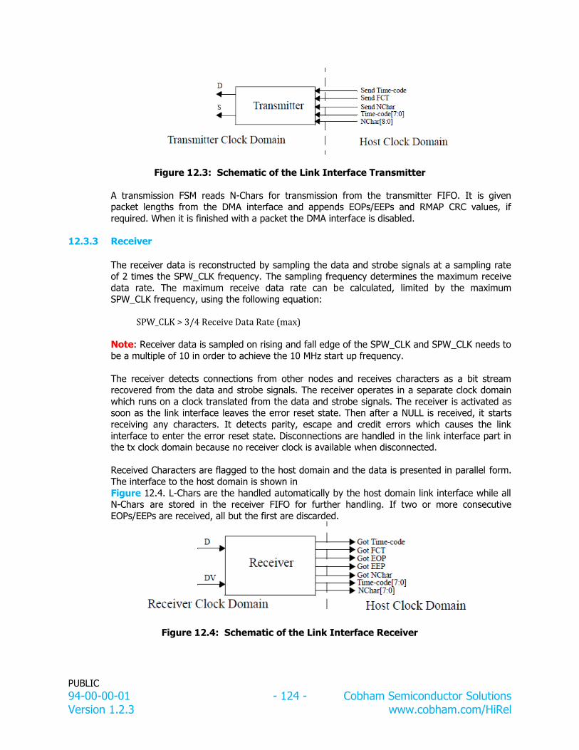
PUBLIC
94-00-00-01 - 124 - Cobham Semiconductor Solutions Version 1.2.3 www.cobham.com/HiRel
Figure 12.3: Schematic of the Link Interface Transmitter
A transmission FSM reads N-Chars for transmission from the transmitter FIFO. It is given packet lengths from the DMA interface and appends EOPs/EEPs and RMAP CRC values, if
required. When it is finished with a packet the DMA interface is disabled.
Receiver 12.3.3
The receiver data is reconstructed by sampling the data and strobe signals at a sampling rate of 2 times the SPW_CLK frequency. The sampling frequency determines the maximum receive
data rate. The maximum receive data rate can be calculated, limited by the maximum SPW_CLK frequency, using the following equation:
SPW_CLK > 3/4 Receive Data Rate (max)
Note: Receiver data is sampled on rising and fall edge of the SPW_CLK and SPW_CLK needs to
be a multiple of 10 in order to achieve the 10 MHz start up frequency.
The receiver detects connections from other nodes and receives characters as a bit stream recovered from the data and strobe signals. The receiver operates in a separate clock domain
which runs on a clock translated from the data and strobe signals. The receiver is activated as soon as the link interface leaves the error reset state. Then after a NULL is received, it starts
receiving any characters. It detects parity, escape and credit errors which causes the link
interface to enter the error reset state. Disconnections are handled in the link interface part in the tx clock domain because no receiver clock is available when disconnected.
Received Characters are flagged to the host domain and the data is presented in parallel form.
The interface to the host domain is shown in
Figure 12.4. L-Chars are the handled automatically by the host domain link interface while all N-Chars are stored in the receiver FIFO for further handling. If two or more consecutive
EOPs/EEPs are received, all but the first are discarded.
Figure 12.4: Schematic of the Link Interface Receiver

PUBLIC
94-00-00-01 - 125 - Cobham Semiconductor Solutions Version 1.2.3 www.cobham.com/HiRel
Time Interface 12.3.4
The time interface is used for sending time-codes over the SpaceWire network and consists of
a time-counter register, time-ctrl register, tick-in signal, tick-out signal, tick-in register field and a tick-out register field. There are also two control register bits which enable the time receiver
and transmitter respectively.
Each time-code sent from the GRSPW2 is a concatenation of the time-ctrl and the time-counter
register. There is a time txen bit which is used to enable time-code transmissions. It is not possible to send time-codes if this bit is zero. Received time-codes are stored to the same time-
ctrl and time-counter registers which are used for transmission. The time rxen bit in the control register is used for enabling time-code reception. No time-codes will be received if this bit is
zero.
The two enable bits are used for ensuring that a node will not accidentally both transmit and
receive time-codes, which violates the SpaceWire standard. It also ensures that the master sending time-codes on a network will not have its time counter overwritten if another (faulty)
node starts sending time-codes.
The time-counter register is set to 0 after reset and is incremented each time the tick-in signal
is asserted for one clock period and the time txen bit is set. This also causes the link interface to send the new value on the network. Tick-in can be generated either by writing a one to the
register field or by asserting the tick-in signal. A Tick-in should not be generated too often since if the time-code after the previous Tick-in has not been sent, the register will not be
incremented and no new value is sent. The tick-in field is automatically cleared when the value
has been sent. Thus, no new ticks should be generated until this field is zero. If the tick-in signal is used there should be at least 4 system-clock and 25 transmit-clock cycles between
each assertion.
A tick-out is generated each time a valid time-code is received and the time rxen bit is set.
When the tick-out is generated, the tick-out signal asserts one clock-cycle and the tick-out register field is asserted until it is cleared by writing a one to it. The current time counter value
can be read from the time register. It is updated each time a time-code is received and the time rxen bit is set. The same register is used for transmissions and can also be written directly
from the APB interface.
The control bits of the time-code are stored to the time-ctrl register when a time-code is
received whose time-count is one more than the nodes current time-counter register. The time-ctrl register can be read through the APB interface. The same register is used during time-code
transmissions.
It is possible to have both the time-transmission and reception functions enabled at the same
time.
12.4 Receiver DMA Channels
The receiver DMA engine handles reception of data from the SpaceWire network to different
DMA channels.
Address Comparison and Channel Selection 12.4.1
Packets are accepted by different channels based on the address and whether a channel is
enabled or not. When the receiver N-Char FIFO contains one or more characters, N-Chars are

PUBLIC
94-00-00-01 - 126 - Cobham Semiconductor Solutions Version 1.2.3 www.cobham.com/HiRel
read by the receiver DMA engine. The first character is interpreted as the logical address and is
compared with the addresses of each channel starting from 0. The packet is stored to the first channel with a matching address. The complete packet including address and protocol ID, but
excluding EOP/EEP, is stored to the memory address pointed to by the descriptors (explained later in this section) of the channel.
Each SpaceWire address register has a corresponding mask register. Only bits at an index containing a zero in the corresponding mask register are compared. This way a DMA channel
can accept a range of addresses. There is a default address register which is used for address checking for RMAP commands in the RMAP target.
If an RMAP command is received, it is only handled by the target if the default address register
(including mask) matches the received address. Otherwise, the packet is stored to a DMA
channel if one or more of them have a matching address. If the address does not match the default address or one of the DMA channels’ separate register, the packet is still handled by the
RMAP target if enabled since it has to return the invalid address error code. The packet is only discarded (up to and including the next EOP/EEP) if an address match cannot be found and the
RMAP target is disabled.
Packets, other than RMAP commands, that do not match the default address register will be
discarded. Figure 12.5 shows a flowchart of packet reception. At least 2 non EOP/EEP N-Chars needs to be received for a packet to be stored to the DMA channel unless the
promiscuous mode is enabled, in which case 1 N-Char is enough. If it is an RMAP packet with hardware RMAP enabled, 3 N-Chars are needed since the command byte determines where the
packet is processed. If the packets are smaller than these sizes they are discarded.
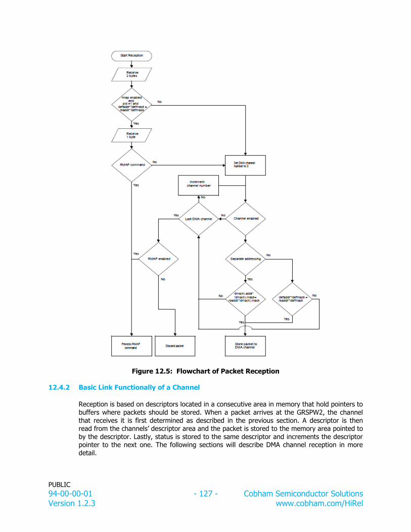
PUBLIC
94-00-00-01 - 127 - Cobham Semiconductor Solutions Version 1.2.3 www.cobham.com/HiRel
Figure 12.5: Flowchart of Packet Reception
Basic Link Functionally of a Channel 12.4.2
Reception is based on descriptors located in a consecutive area in memory that hold pointers to
buffers where packets should be stored. When a packet arrives at the GRSPW2, the channel
that receives it is first determined as described in the previous section. A descriptor is then read from the channels’ descriptor area and the packet is stored to the memory area pointed to
by the descriptor. Lastly, status is stored to the same descriptor and increments the descriptor pointer to the next one. The following sections will describe DMA channel reception in more
detail.

PUBLIC
94-00-00-01 - 128 - Cobham Semiconductor Solutions Version 1.2.3 www.cobham.com/HiRel
Setting up the GRSPW2 for Reception 12.4.3
A few registers need to be initialized before reception to a channel can take place. First, the link interface needs to be put in the run state before any data can be sent. The DMA channel
has a maximum length register which sets the maximum packet size in bytes that can be received to this channel. Larger packets are truncated and the unused portion is discarded. If
this happens, an indication will be given in the status field of the descriptor. The minimum
value for the receiver maximum length field is 4 and the value can only be incremented in steps of four bytes up to the maximum value 33554428. If the maximum length is set to zero,
the receiver will not function correctly.
Either the default address register or the channel specific address register (the accompanying
mask register must also be set) needs to be set to hold the address used by the channel. A control bit in the DMA channel control register determines whether the channel should use
default address and mask registers for address comparison or the channel’s own registers. Using the default register, the same address range is accepted as for other channels with
default addressing and the RMAP target, while the separate address provides the channel its own range.
If all channels use the default registers they will accept the same address range and the enabled channel with the lowest number receives the packet.
Finally, the descriptor table and control register must be initialized. This is described in the two following sections.
Setting up the Descriptor 12.4.4
The GRSPW2 reads descriptors from an area in memory pointed to by the receiver descriptor
register. The register consists of a base address and a descriptor selector. The base address points to the beginning of the area and must start on a 1024 bytes aligned address. It is also
limited to be 1024 bytes in size which means the maximum number of descriptors is 128 since
the descriptor size is 8 bytes.
The descriptor selector points to individual descriptors and is increased by 1 when a descriptor has been used. When the selector reaches the upper limit of the area, it wraps to the
beginning automatically. It can also be set to wrap at a specific descriptor before the upper limit by setting the wrap bit in the descriptor. The idea is that the selector should be initialized
to 0 (start of the descriptor area), but it can also be written with another 8 bytes aligned value
to start somewhere in the middle of the area. It will still wrap to the beginning of the area.
If one wants to use a new descriptor table the receiver enable bit has to be cleared first. When the rx active bit for the channel is cleared it is safe to update the descriptor table register.
When this is finished and descriptors are enabled, the receiver enable bit can be set again.
Enabling Descriptors 12.4.5
As mentioned earlier, one or more descriptors must be enabled before reception can take
place. Each descriptor is 8 bytes in size and should be written to the memory area pointed to by the receiver descriptor register. When new descriptors are added they must always be
placed after the previous one written to the area. Otherwise, they will not be noticed.
A descriptor is enabled by setting the address pointer to point at a location where data can be stored and then setting the enable bit. The WR bit can be set to cause the selector to be set to

PUBLIC
94-00-00-01 - 129 - Cobham Semiconductor Solutions Version 1.2.3 www.cobham.com/HiRel
zero when reception has finished to this descriptor. IE should be set if an interrupt is wanted
when the reception has finished. The DMA control register interrupt enable bit must also be set for an interrupt to be generated.
The descriptor packet address should be word aligned. All accesses on the bus are word
accesses so complete words always overwritten regardless of whether all 32-bit contain
received data. Also, if the packet does not end on a word boundary, the complete word containing the last data byte will be overwritten.
SPWRDW0 Offset = 0x00
Bit# 31 30 29 28 27 26 25 24 23 22 21 20 19 18 17 16
R TR DC HC EP IE WR EN PACKET_LENGTH[24:16]
W
Reset 0 0 0 0 0 0 0 [--…-]
Bit# 15 14 13 12 11 10 9 8 7 6 5 4 3 2 1 0
R PACKET_LENGTH[15:0]
W
Reset [--…-]
Figure 12.6: SpaceWire Receive Descriptor Word 0
Table 12.1: Description of SpaceWire Receive Descriptor Word 0
BIT
NUMBER(S) BIT NAME
RESET
STATE DESCRIPTION
31 TR 0 Truncated Packet was truncated due to maximum length violation.
30 DC 0 Data CRC
0: No data CRC error detected 1: Data CRC error detected
29 HC 0 Header CRC
0: No header CRC error detected 1: Header CRC error detected
28
EP 0 EEP Termination
0: Normal packet termination 1: Packet ended with an Error End of Packet character
27 IE 0 Interrupt Enable
0: No interrupt generated upon packet reception 1: An interrupt generates when a packet has been
received if the Receive Enable interrupt bit in the DMA Channel Control
and Status Register is set.
26 WR 0 Wrap 0: DESCRIPTOR_SELECTOR increases by 0x8 to use the
descriptor at the next memory location. The descriptor table is limited to 1 KB in size and the pointer
automatically wraps back to the base address when it
reaches the 1 KB boundary. 1: The next descriptor used by the GRSPW2 will be the
first one in the descriptor table at the base address.

PUBLIC
94-00-00-01 - 130 - Cobham Semiconductor Solutions Version 1.2.3 www.cobham.com/HiRel
BIT
NUMBER(S) BIT NAME
RESET
STATE DESCRIPTION
25 EN 0 Enable Descriptor 0: Descriptor disabled
1: Descriptor enabled. This means that the descriptor contains valid control values and the memory area
pointed to by the PACKET_ADDRESS field can be used to store a packet.
24-0 Packet Length [--...-] The number of bytes received by the buffer. Only valid
after EN has been set to 0 by the GRSPW2.
SPWRDW1 Offset = 0x04
Bit# 31 30 29 28 27 26 25 24 23 22 21 20 19 18 17 16
R PACKET_ADDRESS[31:16]
W
Reset [--…-]
Bit# 15 14 13 12 11 10 9 8 7 6 5 4 3 2 1 0
R PACKET_ADDRESS[15:2]
00
W
Reset [--…-] 00
Figure 12.7: SpaceWire Receive Descriptor Word 1
Table 12.2: Description of SpaceWire Receive Descriptor Word 1
BIT
NUMBER(S) BIT NAME
RESET
STATE DESCRIPTION
31-2 Packet Address [--…-] The address pointing to the buffer which will be used to store the received packet.
1-0 Packet Address 00 VHDL generics are both set to zero
Setting up the DMA Control Register 12.4.6
The final step to receive packets is to set the control register in the following steps. The receiver must be enabled by setting the rxen bit in the DMA control register (see Section
12.9). This can be done anytime and before this bit is set nothing will happen. The rxdescav bit in the DMA control register is then set to indicate that there are new active descriptors. This
must always be done after the descriptors have been enabled or the GRSPW2 might not notice the new descriptors. More descriptors can be activated when reception has already started by
enabling the descriptors and writing the rxdescav bit. When these bits are set reception starts
immediately when data is arriving.
The Effect to the Control Bits during Reception 12.4.7
When the receiver is disabled all packets going to the DMA-channel are discarded if the
packet’s address does not fall into the range of the DMA channel. If the receiver is enabled and the address falls into the accepted address range, the next state is entered where the rxdescav
bit is checked. This bit indicates whether there are active descriptors or not and should be set by the external application using the DMA channel each time descriptors are enabled as
mentioned above. If the rxdescav bit is ‘0’ and the nospill bit is ‘0’, the packets are discarded. If

PUBLIC
94-00-00-01 - 131 - Cobham Semiconductor Solutions Version 1.2.3 www.cobham.com/HiRel
nospill is one, the GRSPW2 waits until rxdescav is set and the characters are kept in the N-Char
FIFO during this time. If the FIFO becomes full, further N-char transmissions are inhibited by stopping the transmission of FCTs.
When rxdescav is set the next descriptor is read and, if enabled, the packet is received to the
buffer. If the read descriptor is not enabled, rxdescav is set to ‘0’ and the packet spills
depending on the value of nospill. The receiver can be disabled at any time and stops packets from being received to this channel. If a packet is currently received when the receiver is
disabled, the reception still finishes. The rxdescav bit can also be cleared at any time. It will not affect any ongoing receptions, but no more descriptors are read until it is set again. Rxdescav
is also cleared by the GRSPW2 when it reads a disabled descriptor.
Status Bits 12.4.8
When the reception of a packet is finished, the enable bit in the current descriptor is set to
zero. When enable is zero, the status bits are also valid and the number of received bytes is indicated in the length field. The DMA control register contains a status bit which is set each
time a packet has been received. The GRSPW2 can also generate an interrupt for this event.
The RMAP CRC calculation is always active for all received packets and all bytes except the
EOP/EEP are included. The packet is always assumed to be a RMAP packet and the length of the header is determined by checking byte 3 which should be the command field. The
calculated CRC value is then checked when the header has been received (according to the calculated number of bytes) and if it is non-zero, the HC bit sets indicating a header CRC error.
The CRC value is not set to zero after the header has been received. Instead, the calculation continues in the same way until the complete packet has been received. Then, if the CRC value
is non-zero, the DC bit sets indicating a data CRC error.
This means that the GRSPW2 can indicate a data CRC error even if the data field was correct
when the header CRC was incorrect. However, the data should not be used when the header is corrupt; therefore, the DC bit is unimportant in this case. When the header is not corrupted,
the CRC value always is zero when the calculation continues with the data field and the behavior will be as if the CRC calculation was restarted.
If the received packet is not of RMAP type, the header CRC error indication bit cannot be used. It is still possible to use the DC bit if the complete packet is covered by a CRC calculated using
the RMAP CRC definition. This is because the GRSPW2 does not restart the calculation after the header has been received, but instead calculates a complete CRC over the packet. Thus, any
packet format with one CRC at the end of the packet calculated according to RMAP standard can be checked using the DC bit. If the packet is neither of RMAP type nor of the type above,
with RMAP CRC at the end, then both the HC and DC bits should be ignored.
Error Handling 12.4.9
If a packet reception needs to be aborted because of congestion on the network, the
suggested solution is to set link disable to ‘1’. Unfortunately, this also causes the packet
currently being transmitted to be truncated, but this is the only safe solution since packet reception is a passive operation depending on the transmitter at the other end. A channel reset
bit could be provided, but is not a satisfactory solution since the untransmitted characters would still be in the transmitter node. The next character (somewhere in the middle of the
packet) would be interpreted as the node address which would probably cause the packet to be discarded, but not with 100% certainty. Usually this action is performed when a reception has

PUBLIC
94-00-00-01 - 132 - Cobham Semiconductor Solutions Version 1.2.3 www.cobham.com/HiRel
stuck because of the transmitter not providing more data. The channel reset would not resolve
this congestion.
If an AHB error occurs during reception, the current packet is spilled, up to and including, the next EEP/EOP and then the currently active channel is disabled and the receiver enters the idle
state. A bit in the channels control/status register is set to indicate this condition.
Promiscuous Mode 12.4.10
The GRSPW2 supports a promiscuous mode where all the data received is stored to the first
DMA channel enabled regardless of the node address and possible early EOPs/EEPs. This means that all non-eop/eep N-Chars received will be stored to the DMA channel. The
rxmaxlength register is still checked and packets exceeding this size are truncated. RMAP
commands are handled by it when promiscuous mode is enabled if the rmapen bit is set. If it is cleared, RMAP commands are also be stored to a DMA channel.
12.5 Transmitter DMA Channels
The transmitter DMA engine handles transmission of data from the DMA channels to the SpaceWire network. Each receive channel has a corresponding transmit channel which means
there can be up to 4 transmit channels. It is only necessary to use a separate transmit channel for each receive channel if there are also separate entities controlling the transmissions. The
use of a single channel with multiple controlling entities would cause them to corrupt each
other’s transmissions. A single channel is more efficient and should be used when possible.
Multiple transmit channels with pending transmissions are arbitrated in a round-robin fashion.
Basic Functionality of a Channel 12.5.1
A transmit DMA channel reads data from the AHB bus and stores them in the transmitter FIFO
for transmission on the SpaceWire network. Transmission is based on the same type of descriptors as for the receiver and the descriptor table has the same alignment and size
restrictions. When there are new descriptors enabled, the GRSPW2 reads them and transfers the amount data indicated.
Setting up the GRSPW2 for Transmission 12.5.2
Four steps need to be performed before transmissions can be done with the GRSPW2. First, the link interface must be enabled and started by writing the appropriate value to the ctrl
register. Then, the address to the descriptor table needs to be written to the transmitter descriptor register and one or more descriptors must also be enabled in the table. Finally, the
txen bit in the DMA control register is written with a one which triggers the transmission. These
steps are covered in more detail in the next sections.
Enable Descriptors 12.5.3
The descriptor register works in the same way as the receivers corresponding register which
was covered in Section 12.4. The maximum size is 1024 bytes as for the receiver, but since the descriptor size is 16 bytes the number of descriptors is 64.
To transmit packets, one or more descriptors have to be initialized in memory which is done in
the following way. The number of bytes to be transmitted and a pointer to the data has to be
set. There are two different length and address fields in the transmit descriptors because there

PUBLIC
94-00-00-01 - 133 - Cobham Semiconductor Solutions Version 1.2.3 www.cobham.com/HiRel
are separate pointers for header and data. If a length field is zero, the corresponding part of a
packet is skipped and, if both are zero, no packet is sent. The maximum header length is 255 bytes and the maximum data length is 16 Mbyte - 1. When the pointer and length fields have
been set, the enable bit should be set to enable the descriptor. This must always be done last. The other control bits must also be set before enabling the descriptor.
The transmit descriptors are 16 bytes in size so the maximum number in a single table is 64. The different fields of the descriptor, together with the memory offsets, are shown in the tables
below.
The HC bit should be set if RMAP CRC should be calculated and inserted for the header field and correspondingly, the DC bit should be set for the data field. The header CRC are calculated
from the data fetched from the header pointer and the data CRC is generated from data
fetched from the data pointer. The CRCs are appended after the corresponding fields. The NON-CRC bytes field is set to the number of bytes in the beginning of the header field that
should not be included in the CRC calculation.
The CRCs are sent even if the corresponding length is zero. When both lengths are zero no
packet are sent not even an EOP.
Starting Transmission 12.5.4
When the descriptors have been initialized, the transmit enable bit in the DMA control register has to be set to tell the GRSPW2 to start transmitting. New descriptors can be activated in the
table as needed (while transmission is active). Each time a set of descriptors is added the
transmit enable register bit should be set. This has to be done because each time the GRSPW2 encounters a disabled descriptor this register bit is set to 0.
SPWTDW0 Offset = 0x00
Bit# 31 30 29 28 27 26 25 24 23 22 21 20 19 18 17 16
R DC HC
W
Reset [--…-] -- --
Bit# 15 14 13 12 11 10 9 8 7 6 5 4 3 2 1 0
R LE IE WR EN NON_CRC_BYTES[3:0] HEADER_LENGTH[7:0]
W
Reset -- -- -- -- -- [--…-]
Figure 12.8: SpaceWire Transmitter Descriptor Word 0
Table 12.3: Description of SpaceWire Transmitter Descriptor Word 0
BIT NUMBER(S)
BIT NAME RESET STATE
DESCRIPTION
31-18 RESERVED [--...-] 17 DC - Append data CRC
Append CRC calculated according to the RMAP specification after the data sent from the data pointer.
The CRC covers all the bytes from this pointer. A null CRC will be sent if the length of the data field is zero.

PUBLIC
94-00-00-01 - 134 - Cobham Semiconductor Solutions Version 1.2.3 www.cobham.com/HiRel
BIT
NUMBER(S) BIT NAME
RESET
STATE DESCRIPTION
16 HC - Append header CRC (HC) - Append CRC calculated according to the RMAP specification after the data sent
from the header pointer. The CRC covers all bytes from this pointer except a number of bytes in the beginning
specified by the non-crc bytes field. The CRC will not be sent if the header length field is zero.
15 LE - Link Error
0: No link error occurred 1: A link error occurred during the transmission of this
packet
14 IE - Interrupt Enable 0: Disable interrupts
1: An interrupt generates when the packet has been transmitted and the Transmitter Interrupt TE enable bit
in the DMA control register is set.
13 WR - Wrap 0: The descriptor pointer is increased with 0x10 to use
the descriptor at the next higher memory location.
1: The descriptor pointer wraps and the next descriptor read will be the first one in the table (at the base
address).
12 EN - Enable
0: Disable transmitter descriptor
1: Enable transmitter descriptor. When all control fields (address, length, wrap and crc) are set, this bit should be
set. While the bit is set the descriptor should not be modified since this might corrupt the transmission in
progress. The GRSPW2 clears this bit when the
transmission has finished.
11-8 NON_CRC_B YTES [--...-] Sets the number of bytes in the beginning of the header
which should not be included in the CRC calculation. This
is necessary when using path addressing since one or more bytes in the beginning of the packet might be
discarded before the packet reaches its destination.
7-0 HEADER_LENGTH [--...-] Header length in bytes. If set to zero, the header is
skipped.
SPWTDW1 Offset = 0x04
Bit# 31 30 29 28 27 26 25 24 23 22 21 20 19 18 17 16
R HEADER_ADDRESS[31:16]
W
Reset [--…-]
Bit# 15 14 13 12 11 10 9 8 7 6 5 4 3 2 1 0
R HEADER_ADDRESS[15:0]
W
Reset [--…-]
Figure 12.9: SpaceWire Transmitter Descriptor Word 1

PUBLIC
94-00-00-01 - 135 - Cobham Semiconductor Solutions Version 1.2.3 www.cobham.com/HiRel
Table 12.4: Description of SpaceWire Transmitter Descriptor Word 1
BIT
NUMBER(S) BIT NAME
RESET
STATE DESCRIPTION
31-0 HEADER_ADDRESS [--...-] Address from where the packet header is fetched. Does not need to be word aligned.
SPWTDW2 Offset = 0x08
Bit# 31 30 29 28 27 26 25 24 23 22 21 20 19 18 17 16
R DATA_LENGTH[23:16]
W
Reset [00…0] [00…0]
Bit# 15 14 13 12 11 10 9 8 7 6 5 4 3 2 1 0
R DATA_LENGTH[15:0]
W
Reset [00…0]
Figure 12.10: SpaceWire Transmitter Descriptor Word 2
Table 12.5: Description of SpaceWire Transmitter Descriptor Word 2
BIT NUMBER(S)
BIT NAME RESET STATE
DESCRIPTION
31-24 RESERVED [00...0] 23-0 DATA_LENGTH [00...0] Length of data part of the packet in bytes. If set to zero,
no data will be sent. If both data- and header-lengths are set to zero, no packet will be sent.
SPWTDW3 Offset = 0x0C
Bit# 31 30 29 28 27 26 25 24 23 22 21 20 19 18 17 16
R DATA_ADDRESS[31:16]
W
Reset [00…0]
Bit# 15 14 13 12 11 10 9 8 7 6 5 4 3 2 1 0
R DATA_ADDRESS[15:0]
W
Reset [00…0]
Figure 12.11: SpaceWire Transmitter Descriptor Word 3
Table 12.6: Description of SpaceWire Transmitter Descriptor Word 3
BIT
NUMBER(S) BIT NAME
RESET
STATE DESCRIPTION
31-0 DATA_ADDRESS [00...0] Address from where data is read. Does not need to be word aligned.

PUBLIC
94-00-00-01 - 136 - Cobham Semiconductor Solutions Version 1.2.3 www.cobham.com/HiRel
The Transmission Process 12.5.5
When the txen bit is set, the GRSPW2 starts reading descriptors immediately. The number of
bytes indicated is read and transmitted. When a transmission has finished, status is written to the first field of the descriptor and a packet sent bit is set in the DMA control register. If an
interrupt was requested, it also generates. Then a new descriptor is read and, if enabled, a
new transmission starts; otherwise, the transmit enable bit clears and nothing happens until it is enabled again.
The Descriptor Register 12.5.6
The internal pointer which is used to keep the current position in the descriptor table can be
read and written through the APB interface. This pointer is set to zero during reset and is
incremented each time a descriptor is used. It wraps automatically when the 1024 bytes limit for the descriptor table is reached or it can be set to wrap earlier by setting a bit in the current
descriptor.
The descriptor table register can be updated with a new table anytime when no transmission is
active. No transmission is active if the transmit enable bit is zero and the complete table has been sent or if the table is aborted (explained below). If the table is aborted, one has to wait
until the transmit enable bit is zero before updating the table pointer.
Error Handling 12.5.7
Abort TX
The DMA control register contains a bit called Abort TX which if set causes the current transmission to be aborted, the packet is truncated and an EEP is inserted. This is only useful if
the packet needs to be aborted because of congestion on the SpaceWire network. If the congestion is on the AHB bus, this will not help.
Note: This should not be a problem since AHB slaves should have a maximum of 16 waitstates. The aborted packet has its LE bit set in the descriptor. The transmit enable register
bit is also cleared and no new transmissions are done until the transmitter is enabled again.
AHB Error
When an AHB error is encountered during transmission, the currently active DMA channel is
disabled and the transmitter goes to the idle mode. A bit in the DMA channels control/status
register sets to indicate this error condition and, if enabled, an interrupt will also be generated. Further, error handling depends on what state the transmitter DMA engine was in when the
AHB error occurred. If the descriptor was being read and the packet transmission had not been started yet, no more actions are needed.
If the AHB error occurs during packet transmission, the packet is truncated and an EEP is inserted. Lastly, if it occurs when status is written to the descriptor, the packet has been
successfully transmitted, but the descriptor is not written and continues to be enabled (this also means that no error bits are set in the descriptor for AHB errors).The client using the channel
has to correct the AHB error condition and enable the channel again. No more AHB transfers
are done again from the same unit (receiver or transmitter) which was active during the AHB error until the error state is cleared and the unit is enabled again.

PUBLIC
94-00-00-01 - 137 - Cobham Semiconductor Solutions Version 1.2.3 www.cobham.com/HiRel
Link Error
When a link error occurs during the transmission, the remaining part of the packet is discarded up to and including the next EOP/EEP. When this is done, status is immediately written (with
the LE bit set) and the descriptor pointer is incremented. The link will be disconnected when the link error occurs, but the GRSPW2 automatically tries to connect again provided that the
link-start bit is asserted and the link-disabled bit is deasserted. If the LE bit in the DMA
channel’s control register is not set the transmitter DMA engine waits for the link to enter run-state and start a new transmission immediately, when possible, if packets are pending.
Otherwise, the transmitter is disabled when a link error occurs during the transmission of the current packet and no more packets are transmitted until it is enabled again immediately, when
possible, if packets are pending.
12.6 Remote Memory Access Protocol (RMAP) The Remote Memory Access Protocol (RMAP) is used to implement access to resources in the
node via the SpaceWire Link. Some common operations are reading and writing to memory, registers and FIFOs. This section describes the basics of the RMAP protocol and the target
implementation.
Fundamentals of the Protocol 12.6.1
RMAP is a protocol which is designed to provide remote access via a SpaceWire network to
memory mapped resources on a SpaceWire node. It has been assigned protocol ID 0x01. It
provides three operations: write, read and read-modify-write. These operations are posted operations, which means that a source does not wait for an acknowledgement or reply. It also
implies that any number of operations can be outstanding at any time and that no timeout mechanism is implemented in the protocol. Time-outs must be implemented in the user
application which sends the commands. Data payloads of up to 16 MB - 1 are supported in the protocol. A destination can be requested to send replies and to verify data before executing an
operation. A complete description of the protocol is found in the RMAP standard.
Implementation 12.6.2
The GRSPW2 includes a target for RMAP commands which processes all incoming packets with
protocol ID = 0x01, type field (bit 7 and 6 of the 3rd byte in the packet) equal to 01b and an
address falling in the range set by the default address and mask register. When such a packet is detected, it is not stored to the DMA channel, instead it is passed to the RMAP receiver. The
GRSPW2 implements all three commands defined in the standard with some restrictions. Support is only provided for 32-bit big-endian systems. This means that the first byte received
is the MSB in a word. The target will not receive RMAP packets using the extended protocol ID which are always dumped to the DMA channel.
The RMAP receiver processes commands. If they are correct and accepted, the operation is performed on the AHB bus and a reply is formatted. If an acknowledgement is requested, the
RMAP transmitter automatically sends the reply. RMAP transmissions have priority over DMA channel transmissions. There is a user accessible destination key register which is compared to
destination key field in incoming packets. If there is a mismatch and a reply has been
requested, the error code in the reply is set to 3. Replies are sent if and only if the ack field is set to ‘1’.

PUBLIC
94-00-00-01 - 138 - Cobham Semiconductor Solutions Version 1.2.3 www.cobham.com/HiRel
When a failure occurs during a bus access, the error code is set to 1 (General Error). There is
predetermined order in which error-codes are set in the case of multiple errors in the GRSPW2. It is shown in Table 12.7.
Table 12.7: SpaceWire RMAP Packet Error Codes and Detection Order (Highest Priority is 1)
DETECTION
ORDER ERROR CODE
ERROR ERROR DESCRIPTION
APPLICABILITY
WRITE READ RMW
8 7 EEP EEP marker detected
immediately after the header CRC or during the transfer of
data and Data CRC or immediately thereafter
indicates that there was a
communication failure of some sort on the network.
X X X
NA 8 RESERVED 4 9 Verify buffer
overrun
The verify before write bit of
the command was set so that the data field was
buffered in order to verify the Data CRC before
transferring the data to
target memory. The data field was longer than able to
fit inside the verify buffer resulting in a buffer overrun.
Note: The command is not
executed in this case.
X X
6 10 Authorization
failure
The target user application
did not authorize the requested operation. This
may be because the
command requested has not been implemented.
X X X
5 11 RMW Data
Length error
The amount of data in a
RMW command is invalid (0x01,
0x03, 0x05, 0x07 or greater than 0x08).
X
1 12 Invalid
destination target logical
address
The Header CRC was
decoded correctly but the Target
Logical Address was not the value expected by the target.
X X X
Note: The AHB error is not guaranteed to be detected before Early EOP/EEP or Invalid Data CRC. For very long accesses, the AHB error detection might be delayed causing the other two
errors to appear first.
Read accesses are performed as needed. They are not stored in a temporary buffer before
transmitting. This means that the error code 1 will never be seen in a read reply since the

PUBLIC
94-00-00-01 - 139 - Cobham Semiconductor Solutions Version 1.2.3 www.cobham.com/HiRel
header has already been sent when the data is read. If the AHB error occurs the packet is
truncated and ended with an EEP.
Errors up to, and including Invalid Data CRC (number 8), are checked before verified commands. The other errors do not prevent verified operations from being performed. The
details of the support for the different commands are now presented. All defined commands
which are received, but have an option set which is not supported in this specific implementation, will not be executed and a possible reply is sent with error code 10.
Write Commands 12.6.3
The write commands are divided into two subcategories when examining their capabilities:
verified writes and non-verified writes. Verified writes have a length restriction of 4 bytes and
the address must be aligned to the size. That is 1 byte writes can be done to any address, 2 bytes must be half word aligned, 3 bytes are not allowed and 4 bytes writes must be word
aligned. Since there will always be only an AHB operation performed for each RMAP verified write command, the incrementing address bit can be set to any value.
Non-verified writes have no restrictions when the incrementing bit is set to 1. If it is set to 0 the number of bytes must be a multiple of 4 and the address word aligned. There is no
guarantee how many words are written when early EOP/EEP is detected for non-verified writes.
Read Commands 12.6.4
Read commands are performed as needed when the reply is sent. Thus, if an AHB error occurs,
the packet truncates and ends with an EEP. There are no restrictions for incrementing reads, but non-incrementing reads have the same alignment restrictions as non-verified writes.
Note: The “Authorization failure” error code is sent in the reply if a violation was detected
even if the length field was zero. Also, no data is sent in the reply if an error was detected, i.e.
if the status field is non-zero.
Read-Modify-Write Commands 12.6.5
All read-modify-write sizes are supported except 6 which would have caused 3 B being read
and written on the bus. The RMW bus accesses have the same restrictions as the verified writes. As in the verified write case, the incrementing bit can be set to any value since only one
AHB bus operation will be performed for each RMW command. Cargo too large is detected after the bus accesses so this error will not prevent the operation from being performed. No data is
sent in a reply if an error is detected, i.e., the status field is non-zero.
Controls 12.6.6
The RMAP target mostly runs in the background without any external intervention, but there are
a few control possibilities. There is an enable bit in the control register of the GRSPW2 which can be used to completely disable the RMAP target.
When it is set to ‘0’ no RMAP packets will be handled in hardware, instead they are all stored to the DMA channel. There is a possibility that RMAP commands will not be performed in the order
they arrive. This can happen if a read arrives before one or more writes. Since the target stores replies in a buffer with more than one entry several commands can be processed even if no
replies are sent. Data for read replies is read when the reply is sent and thus writes coming after the read might have been performed already if there was congestion in the transmitter. To

PUBLIC
94-00-00-01 - 140 - Cobham Semiconductor Solutions Version 1.2.3 www.cobham.com/HiRel
avoid this, the RMAP buffer disable bit can be set to force the target to only use one buffer
which prevents this situation.
The last control option for the target is the possibility to set the destination key which is found in a separate register.
Table 12.8: GRSPW2 Hardware RMAP Handling of Different Packet Type and Command Fields
PACKET TYPE RMAP COMMAND CODES COMMAND ACTION
BIT 7 BIT6 BIT 5 BIT4 BIT 3 BIT 2
Reserved Command
/
Response
Write
/Read
Verify
data
before write
Acknow
-ledge
Increment
Address
0 0 - - - - Response Stored to DMA-channel
0 1 0 0 0 0 Not used Does nothing. No reply is sent.
0 1 0 0 0 1 Not used Does nothing. No reply
is sent.
0 1 0 0 1 0 Read single
address
Executed normally.
Address has to be word aligned and data size a
multiple of four. Reply is
sent. If alignment restrictions are violated
error code is set to 10.
0 1 0 0 1 1 Read incrementing
address.
Executed normally. No restrictions. Reply is
sent.
0 1 0 1 0 0 Not used Does nothing. No reply
is sent.
0 1 0 1 0 1 Not used Does nothing. No reply is sent.
0 1 0 1 1 0 Not used Does nothing. Reply is
sent with error code 2.
0 1 0 1 1 1 Read-Modify- Write
incrementing address
Executed normally. If length is not one of the
allowed RMW values nothing is done and
error code is set to 11. If the length was
correct, alignment
restrictions are checked next. 1 byte can be
RMW to any address. 2 bytes must be halfword
aligned. 3 bytes are not
allowed. 4 bytes must be word aligned. If
these restrictions are violated nothing is done
and error code is set to

PUBLIC
94-00-00-01 - 141 - Cobham Semiconductor Solutions Version 1.2.3 www.cobham.com/HiRel
PACKET TYPE RMAP COMMAND CODES COMMAND ACTION
BIT 7 BIT6 BIT 5 BIT4 BIT 3 BIT 2
Reserved Command /
Response
Write /Read
Verify data
before write
Acknow-ledge
Increment Address
10. If an AHB error
occurs error code is set to 1. Reply is sent.
0 0 - - - - Response Stored to DMA-channel
0 1 1 0 0 0 Write, single- address, do
not verify
before writing, no
acknowledge
Executed normally. Address has to be word
aligned and data size a
multiple of four. If alignment is violated
nothing is done. No reply is sent.
0 1 1 0 0 1 Write,
incrementing address, do
not verify before
writing, no
acknowledge
Executed normally. No
restrictions. No reply is sent.
0 1 1 0 1 0 Write, single-
address, do
not verify before
writing, send acknowledge
Executed normally.
Address has to be word
aligned and data size a multiple of four. If
alignment is violated nothing is done and
error code is set to 10. If an AHB error occurs
error code is set to 1.
Reply is sent.
0 1 1 0 1 1 Write,
incrementing
address, do not verify
before writing, send
acknowledge
Executed normally. No
restrictions. If AHB
error occurs error code is set to 1. Reply is
sent.
0 1 1 1 0 0 Write, single address,
verify before writing, no
acknowledge
Executed normally. Length must be 4 or
less. Otherwise nothing is done. Same
alignment restrictions
apply as for RMW. No reply is sent.
0 1 1 1 0 1 Write,
incrementing address,
verify before
Executed normally.
Length must be 4 or less. Otherwise nothing
is done. Same

PUBLIC
94-00-00-01 - 142 - Cobham Semiconductor Solutions Version 1.2.3 www.cobham.com/HiRel
PACKET TYPE RMAP COMMAND CODES COMMAND ACTION
BIT 7 BIT6 BIT 5 BIT4 BIT 3 BIT 2
Reserved Command /
Response
Write /Read
Verify data
before write
Acknow-ledge
Increment Address
writing, no
acknowledge
alignment restrictions
apply as for RMW. If they are violated
nothing is done. No
reply is sent.
0 1 1 1 1 0 Write, single
address, verify before
writing, send
acknowledge
Executed normally.
Length must be 4 or less. Otherwise nothing
is done and error code
is set to 9. Same alignment restrictions
apply as for RMW. If they are violated
nothing is done and
error code is set to 10. If an AHB error occurs
error code is set to 1. Reply is sent.
0 1 1 1 1 1 Write,
incrementing address,
verify before writing, send
acknowledge
Executed normally.
Length must be 4 or less. Otherwise nothing
is done and error code is set to 9. Same
alignment restrictions
apply as for RMW. If they are violated
nothing is done and error code is set to 10.
If an AHB error occurs
error code is set to 1. Reply is sent.
1 0 - - - - Unused Stored to DMA-channel.
1 1 - - - - Unused Stored to DMA-
channel.
12.7 AMBA Interface
The AMBA interface consists of an APB interface, an AHB master interface and DMA FIFOs. The
APB interface provides access to the user registers which are described in Section 12.9. The
DMA engines have 32-bit wide FIFOs to the AHB master interface which are used when reading and writing to the bus. The transmitter DMA engine reads data from the bus in bursts which
are half the FIFO size in length. A burst is always started when the FIFO is half-empty or if it can hold the last data for the packet. The burst containing the last data might have shorter
length if the packet is not an even number of bursts in size.

PUBLIC
94-00-00-01 - 143 - Cobham Semiconductor Solutions Version 1.2.3 www.cobham.com/HiRel
The receiver DMA works in the same way except that it checks if the FIFO is half-full and then
performs a burst write to the bus which is half the F size in length. The last burst might be shorter. If the rmap or rxunaligned VHDL generics are set to 1, the interface also handles byte
accesses. Byte accesses are used for non-word-aligned buffers and/or packet lengths that are not a multiple of four bytes. There might be 1 to 3 single byte writes when writing the
beginning and end of the received packets.
APB Slave Interface 12.7.1
As mentioned above, the APB interface provides access to the user registers which are 32-bits in
width. The accesses to this interface are required to be aligned word accesses. The result is undefined if this restriction is violated.
AHB Master Interface 12.7.2
The GRSPW2 contains a single master interface which is used by both the transmitter and receiver DMA engines. The arbitration algorithm between the channels is done so that if the
current owner requests the interface again, it will always acquire it. This will not lead to
starvation problems since the DMA engines always deassert their requests between accesses. The AHB accesses can be of size byte, halfword and word (HSIZE = 0x000, 0x001, 0x010)
otherwise. Byte and halfword accesses are always NONSEQ.
Note: Read accesses are always word accesses (HSIZE=0x010), which can result in a destructive read.
The burst length will be half the AHB FIFO size except for the last transfer for a packet which might be smaller. Shorter accesses are also done during descriptor reads and status writes.
The AHB master also supports non-incrementing accesses where the address will be constant for several consecutive accesses. HTRANS will always be NONSEQ in this case while for
incrementing accesses it is set to SEQ after the first access. This feature is included to support
non-incrementing reads and writes for RMAP.
If the GRSPW2 does not need the bus after a burst has finished, there will be one wasted cycle (HTRANS = IDLE).
BUSY transfer types are never requested and the GRSPW2 provides full support for ERROR, RETRY and SPLIT responses.
12.8 SpaceWire Clock Generation The clock source for SpaceWire core is the SPW_CLK input.
The SpaceWire transmit clock must be a multiple of 10 MHz in order to achieve the 10 MHz start
up frequency. The division to 10 MHz is done internally in the GRSPW2 core. During reset the clock link divider register in GRSPW2 gets its value from GPIO[7:4], which must be pulled
up/down to set the divider correctly. Thus, it is possible to use a SPW_CLK which is any multiple of 10 between 10-150MHz.
Note: The required precision is 10 MHz ± 1MHz.
12.9 Register
The UT699E/UT700 has four SpaceWire nodes, each comprised of a GRSPW2 core. Each core
has its own set of registers mapped into APB memory space. The APB address mapping for

PUBLIC
94-00-00-01 - 144 - Cobham Semiconductor Solutions Version 1.2.3 www.cobham.com/HiRel
each GRSPW2 core is listed in Table 1.3. The relative offset of each register is shown in Table
12.9 below. All GRSPW2 cores have RMAP functionality, so any RMAP registers apply to these cores.
Table 12.9: GRSPW2 Registers
REGISTER APB ADDRESS
OFFSET
SPW Control Register (SPWCTR) 0x0
SPW Status Register (SPWSTR) 0x4
SPW Node Address Register (SPWNDR) 0x8
SPW Clock Divisor Register (SPW_CLK) 0xC
SPW Destination Key Register (SPWKEY) 0x10
SPW Time Register (SPWTIM) 0x14
Reserved 0x18
SPW DMA Channel Control and Status Register (SPWCHN) 0x20
SPW DMA Channel Receiver Maximum Length Register (SPWRXL) 0x24
SPW DMA Transmit Descriptor Register (SPWTXD) 0x28
SPW DMA Receive Descriptor Register (SPWRXD) 0x2C
DMA Channel address register 0x30
SPWCTR
Address = 0x8000_0A00
Address = 0x8000_0B00 Address = 0x8000_0C00
Address = 0x8000_0D00
Bit# 31 30 29 28 27 26 25 24 23 22 21 20 19 18 17 16
R RA RX RC PO LOOP RD RE
W
Reset 1 0 1 00 0 000 0 0000 0 1
Bit# 15 14 13 12 11 10 9 8 7 6 5 4 3 2 1 0
R TR TT LI TQ RS PM TI IE AS LS LD
W
Reset 0000 0 0 -- -- 0 0 0 0 0 - 1 0
Figure 12.12: SpaceWire Control Register
Table 12.10: Description of SpaceWire Control Register
BIT
NUMBER(S) BIT NAME
RESET
STATE DESCRIPTION
31 RA 1 RMAP Available
0: RMAP unavailable
1: Set to one if the RMAP command handler is available Read=0; Write=don’t care
30 RX 0 RX Unaligned Access 0: Unaligned writes not available for the receiver
1: Unaligned writes available for the receiver Read=0;
Write=don’t care
29 RC 1 RMAP CRC Available
0: RMAP CRC not available
1: RMAP CRC available Read=0; Write=don’t care.

PUBLIC
94-00-00-01 - 145 - Cobham Semiconductor Solutions Version 1.2.3 www.cobham.com/HiRel
BIT
NUMBER(S) BIT NAME
RESET
STATE DESCRIPTION
28-27 RESERVED 00 26 PO 0 Number of available SpaceWire ports minus 1
25-23 RESERVED 000 22 Loop 0 Port loop back:
0: Loop back disable
1: Tx is internally looped to Rx
21-18 RESERVED 0000 17 RD 0 RMAP Buffer Disable
0: All RMAP buffers are used
1: Only one RMAP buffer is used. This ensures that all RMAP commands are executed consecutively.
16 RE 1 RMAP Enable
0: Disable RMAP command handler 1: Enable RMAP command handler
15-12 RESERVED 0000 11 TR 0 Time RX Enable
0: Disable time-code receptions 1: Enable time-code receptions
10 TT 0 Time TX Enable
0: Disable time-code transmissions 1: Enable time-code transmissions
9 LI - Link Error IRQ
0: No interrupt 1: Generate interrupt when a link error occurs. Not reset.
8 TQ - Tick-Out IRQ
0: No interrupt 1: Generate interrupt when a valid time-code is received.
Not reset.
7 RESERVED 0 6 RS 0 Reset
0: No action
1: Make complete reset of the SpaceWire node. Self-clearing.
5 PM 0 Promiscuous Mode
0: Disable 1: Enable
4 TI 0 Tick In
The host can generate a tick by writing a one to this field. This increment the timer counter and the new value
is transmitted after the current character is transferred.
3 IE 0 Interrupt Enable 0: No interrupt
1: Interrupt is generated when a bit 8 or 9 is set and its corresponding event occurs.
2 AS - Autostart
0: No effect 1: Automatically start the link when a NULL has been
received. Not reset.
1 LS 1 Link Start

PUBLIC
94-00-00-01 - 146 - Cobham Semiconductor Solutions Version 1.2.3 www.cobham.com/HiRel
BIT
NUMBER(S) BIT NAME
RESET
STATE DESCRIPTION
0: No effect 1: Start the link, i.e., allow a transition from ready to
started state.
0 LD 0 Link Disable
0: No effect
1: Disable the SpaceWire codec.
SPWSTR
Address = 0x8000_0A04
Address = 0x8000_0B04 Address = 0x8000_0C04
Address = 0x8000_0D04
Bit# 31 30 29 28 27 26 25 24 23 22 21 20 19 18 17 16
R LS[2:0]
W
Reset [00…0] 000 [00…0]
Bit# 15 14 13 12 11 10 9 8 7 6 5 4 3 2 1 0
R AP EE IA PE DE ER CE T0
W
Reset [00…0] 0 0 0 00 0 0 0 0 0
Figure 12.13: SpaceWire Status Register
Table 12.11: Description of SpaceWire Status Register
BIT
NUMBER(S) BIT NAME
RESET
STATE DESCRIPTION
31-24 RESERVED [00...0] 23-21 LS 000 Link State
This field indicates the current state of the start-up
sequence. 0: Error-reset
1: Error-wait 2: Ready
3: Started
4: Connecting 5: Run
20-10 RESERVED [00...0] 9 AP 0 Active port
Shows the currently active port. 0: Port 0
1: Port 1 where the port numbers refer to the index number of the
data and strobe signals.
8 EE 0 Early EOP/EEP Read: 0: Packet received normally
1: Packet was received with an EOP after the first byte
for a non- RMAP packet or after the second byte for a

PUBLIC
94-00-00-01 - 147 - Cobham Semiconductor Solutions Version 1.2.3 www.cobham.com/HiRel
BIT
NUMBER(S) BIT NAME
RESET
STATE DESCRIPTION
RMAP packet. Write:
0: No effect 1: Clear bit
7 IA 0 Invalid Address Read:
0: Packet received normally 1: Packet was received with an invalid destination
address field Write:
0: No effect
1: Clear bit
6-5 RESERVED 00 4 PE 0 Parity Error Read:
0: Packet received normally
1: A parity error has occurred Write:
0: No effect 1: Clear bit
3 DE 0 Disconnect Error Read:
0: No disconnection error 1: A disconnection error has occurred
Write: 0: No effect
1: Clear bit
2 ER 0 Escape Error Read: 0: No escape error
1: An escape error has occurred
Write: 0: No effect
1: Clear bit
1 CE 0 Credit Error Read:
0: No credit error
1: A credit has occurred Write:
0: No effect 1: Clear bit
0 TO 0 Tick Out Read:
0: No new time count 1: A new time count value was received and is stored in
the time counter field.
Write: 0: No effect
1: Clear bit

PUBLIC
94-00-00-01 - 148 - Cobham Semiconductor Solutions Version 1.2.3 www.cobham.com/HiRel
SPWNAR
Address = 0x8000_0A08
Address = 0x8000_0B08 Address = 0x8000_0C08
Address = 0x8000_0D08
Bit# 31 30 29 28 27 26 25 24 23 22 21 20 19 18 17 16
R
W
Reset --
Bit# 15 14 13 12 11 10 9 8 7 6 5 4 3 2 1 0
R ADDRESS_MASK[7:0] NODE_ADDRESS[7:0]
W
Reset [00…0] 254
Figure 12.14: SpaceWire Node Address Register
Table 12.12: Description of SpaceWire Node Address Register
BIT
NUMBER(S) BIT NAME
RESET
STATE DESCRIPTION
31-16 RESERVED [--...-] 15-8 ADDRESS_MASK [00...0] Used for masking the address before comparison. Both
the received address and the NODE_ADDRESS fields are
logically ended with the inverse of ADDRESS_MASK before the address check.
7-0 NODE_ADDRESS 254 8-Bit Node Address
Used for node identification on the SpaceWire net- work.
SPWCLK
Address = 0x8000_0A0C
Address = 0x8000_0B0C Address = 0x8000_0C0C
Address = 0x8000_0D0C
Bit# 31 30 29 28 27 26 25 24 23 22 21 20 19 18 17 16
R
W
Reset [00…0]
Bit# 15 14 13 12 11 10 9 8 7 6 5 4 3 2 1 0
R CLOCK_DIVISOR_LINK[7:0] CLOCK_DIVISOR_RUN[7:0]
W
Reset {0000,GPIO[7:4]} {0000,GPIO[7:4]}
Figure 12.15: SpaceWire Clock Divisor Register
Table 12.13: Description of SpaceWire Clock Divisor Register
BIT
NUMBER(S) BIT NAME
RESET
STATE DESCRIPTION
31-16 RESERVED [00...0]

PUBLIC
94-00-00-01 - 149 - Cobham Semiconductor Solutions Version 1.2.3 www.cobham.com/HiRel
BIT
NUMBER(S) BIT NAME
RESET
STATE DESCRIPTION
15-8 CLOCK_DIVISOR_LINK
GPIO[7:4] 8-Bit Clock Divisor Link State Value Used for the clock-divisor when the link-interface is
not in run-state. GPIO[7:4]-- Set the SpaceWire clock divisor link bits
in the SpaceWire Clock Divisor Register Actual divisor value = (CLOCK_DIVISOR_LINK + 1).
7-0 CLOCK_DIVISOR_
RUN
GPIO[7:4] 8-Bit Clock Divisor Run State Value
Used for the clock-divider when the link-interface is in the run-state. Actual divisor value =
(CLOCK_DIVISOR_RUN + 1).
SPWKEY
Address = 0x8000_0A10
Address = 0x8000_0B10
Address = 0x8000_0C10 Address = 0x8000_0D10
Bit# 31 30 29 28 27 26 25 24 23 22 21 20 19 18 17 16
R
W
Reset [00…0]
Bit# 15 14 13 12 11 10 9 8 7 6 5 4 3 2 1 0
R DESTINATION_KEY[7:0]
W
Reset [00…0] [00…0]
Figure 12.16: SpaceWire Destination Key Register
Table 12.14: Description of SpaceWire Destination Key Register
BIT
NUMBER(S) BIT NAME
RESET
STATE DESCRIPTION
31-8 RESERVED [00...0] 7-0 DESTINATION_KEY [00...0] RMAP Destination Key
SPWTIM
Address = 0x8000_0A14
Address = 0x8000_0B14 Address = 0x8000_0C14
Address = 0x8000_0D14
Bit# 31 30 29 28 27 26 25 24 23 22 21 20 19 18 17 16
R
W
Reset [00…0]
Bit# 15 14 13 12 11 10 9 8 7 6 5 4 3 2 1 0
R TIME_CTRL[1:0] TIME_COUNTER[5:0]
W
Reset [00…0] 00 [00…0]

PUBLIC
94-00-00-01 - 150 - Cobham Semiconductor Solutions Version 1.2.3 www.cobham.com/HiRel
Figure 12.17: SpaceWire Time Register
Table 12.15: Description of SpaceWire Time Register
BIT NUMBER(S)
BIT NAME RESET STATE
DESCRIPTION
31-8 RESERVED [00...0] 7-6 TIME_CTRL 00 Time Control Flags
The current value of the time control flags. Sent with time-code resulting from a tick-in. Received control
flags are also stored in this field.
5-0 TIME_COUNTER [00…0] Time Counter The counter represents the system time count. The
counter is incremented each time a time code is received and decoded into a tick-out or when the host
writes to the tick-in bit.
SPWCHN
Address = 0x8000_0A20
Address = 0x8000_0B20 Address = 0x8000_0C20
Address = 0x8000_0D20
Bit# 31 30 29 28 27 26 25 24 23 22 21 20 19 18 17 16
R LE
W
Reset [00…0] 0
Bit# 15 14 13 12 11 10 9 8 7 6 5 4 3 2 1 0
R SP SA EN NS RD
RX AT RA TA PR PS AI RI TI RE TE
W
Reset 0 0 0 0 0 0 0 0 0 0 0 -- -- -- 0 0
Figure 12.18: SpaceWire DMA Channel Control and Status Register
Table 12.16: Description of SpaceWire DMA Channel Control and Status Register
BIT
NUMBER(S) BIT NAME
RESET
STATE DESCRIPTION
31-17 RESERVED [00...0] 16 LE 0 Link error disable
Disable transmitter when a link error occurs. No more
packets are transmitted until the transmitter is enabled
again.
15 SP 0 Strip PID
Remove the PID byte (second byte) of each packet. The address byte (first byte) is also removed when this bit is
set independent of the SA bit.
14 SA 0 Strip Address Remove the address byte (first byte) of each packet.
13 EN 0 Enable Address
Enable separate node address for this channel.

PUBLIC
94-00-00-01 - 151 - Cobham Semiconductor Solutions Version 1.2.3 www.cobham.com/HiRel
BIT
NUMBER(S) BIT NAME
RESET
STATE DESCRIPTION
12 NS 0 No Spill 0: If cleared, packets are discarded when a packet is
arriving and there are no active descriptors. 1: If set, the GRSPW2 waits for a descriptor to be
activated
11 RD 0 RX Descriptors Available Read: 0: Cleared by GRSPW2 when it encounters a disabled
descriptor. 1: Indicates enabled descriptors in the descriptor table.
Write:
0: No active descriptors in the descriptor table. 1: Set to one to indicate to the GRSPW2 that there are
enabled descriptors in the descriptor table.
10 RX 0 RX Active
0: No DMA channel activity
1: Set if a reception to the DMA channel is currently active. (Read Only)
9 AT 0 Abort TX
0: No effect 1: Setting the bit aborts the currently transmitting
packet and disables transmissions. If no transmission is active, the only effect is to disable transmissions. Self-
clearing.
8 RA 0 RX AHB Error 0: No error response
1: An error response was detected on the AHB bus while this receive DMA channel was accessing the bus.
Cleared when written with a one.
7 TA 0 TX AHB Error 0: No error response
1: An error response was detected on the AHB bus while
this transmit DMA channel was accessing the bus. Cleared when written with a one.
6 PR 0 Packet Received 0: No new packet 1: This bit is set each time a packet has been received.
Not self-clearing. Cleared when written with a one.
5 PS 0 Packet Sent 0: No packet sent
1: This bit is set each time a packet has been sent. Not
self-clearing. Cleared when written with a one.
4 AI - AHB Error Interrupt
0: No interrupt will be generated 1: If set, an interrupt generates each time an AHB
error occurs when this DMA channel is accessing the
bus. Not reset.
3 RI - Receive Interrupt
0: No interrupt will be generated
1: If set, an interrupt generates each time a packet has been received. This happens if either the packet is
terminated by an EEP or EOP. Not reset.

PUBLIC
94-00-00-01 - 152 - Cobham Semiconductor Solutions Version 1.2.3 www.cobham.com/HiRel
BIT
NUMBER(S) BIT NAME
RESET
STATE DESCRIPTION
2 TI - Transmit Interrupt 0: No interrupt generates
1: If set, an interrupt generates each time a packet is transmitted. The interrupt is generated regardless of
whether the transmission was successful or not. Not reset.
1 RE 0 Receiver Enable
0: Channel is not allowed to receive packets 1: Channel is allowed to receive packets
0 TE 0 Transmitter Enable Read:
0: Cleared by GRSPW2 when it encounters a disabled descriptor.
1: Indicates enabled descriptors in the descriptor table. Write:
0: No active descriptors in the descriptor table.
1: Set to one to indicate to the GRSPW2 that there are enabled descriptors in the descriptor table. Writing a one
will cause the GRSPW2 to read a new descriptor and try to transmit the packet to which it points.
SPWRXL
Address = 0x8000_0A24 Address = 0x8000_0B24
Address = 0x8000_0C24 Address = 0x8000_0D24
Bit# 31 30 29 28 27 26 25 24 23 22 21 20 19 18 17 16
R RX_MAX_LENGTH[24:16]
W
Reset 000_0000 [--…-]
Bit# 15 14 13 12 11 10 9 8 7 6 5 4 3 2 1 0
R RX_MAX_LENGTH[15:0]
W
Reset [--…-]
Figure 12.19: SpaceWire DMA Channel Receiver Max Length Register
Table 12.17: Description of SpaceWire DMA Channel Receiver Max Length Register
BIT NUMBER(S)
BIT NAME RESET STATE
DESCRIPTION
31-25 RESERVED [00...0] 24-0 RX_MAX_LENGTH [--...-] Receiver Packet Maximum Length
The maximum number of bytes in a packet that may be received. Only bits 24-2 are writable. Bits 1-0
always read 0. Not reset.

PUBLIC
94-00-00-01 - 153 - Cobham Semiconductor Solutions Version 1.2.3 www.cobham.com/HiRel
SPWTXD
Address = 0x8000_0A28
Address = 0x8000_0B28 Address = 0x8000_0C28
Address = 0x8000_0D28
Bit# 31 30 29 28 27 26 25 24 23 22 21 20 19 18 17 16
R TX_BASE_ADDRESS[22:7]
W
Reset [--…-]
Bit# 15 14 13 12 11 10 9 8 7 6 5 4 3 2 1 0
R TX_BASE_ADDRESS[6:0] TX_DESC_SELECT[5:0]
W
Reset [--…-] [00…0] 0000
Figure 12.20: SpaceWire Transmitter Descriptor Register
Table 12.18: Description of SpaceWire Transmitter Descriptor Register
BIT
NUMBER(S) BIT NAME
RESET
STATE DESCRIPTION
31-10 TX_BASE_ADDRESS [--...-] Transmitter Descriptor Table Base Address
Sets the base address of the descriptor table. Not reset.
9-4 TX_DESC_SELECT [00..0] Transmitter Descriptor Selector This is the relative offset into the descriptor table and
indicates which descriptor is currently used by the
GRSPW2. For each new descriptor read, TX_DESC_SELECT increases by one and wrap to zero
when the field increments to 64.
3-0 RESERVED 0000
SPWRXD
Address = 0x8000_0A2C
Address = 0x8000_0B2C
Address = 0x8000_0C2C Address = 0x8000_0D2C
Bit# 31 30 29 28 27 26 25 24 23 22 21 20 19 18 17 16
R RX_BASE_ADDRESS[21:6]
W
Reset [--…-]
Bit# 15 14 13 12 11 10 9 8 7 6 5 4 3 2 1 0
R RX_BASE_ADDRESS[5:0] RX_DESC_SELECT[6:0]
W
Reset [--…-] [00…0] 000
Figure 12.21: SpaceWire Receiver Descriptor Register

PUBLIC
94-00-00-01 - 154 - Cobham Semiconductor Solutions Version 1.2.3 www.cobham.com/HiRel
Table 12.19: Description of SpaceWire Receiver Descriptor Register
BIT
NUMBER(S) BIT NAME
RESET
STATE DESCRIPTION
31-10 RX_BASE_ADDRESS
[--...-] Receiver Descriptor Table Base Address Sets the base address of the descriptor table. Not reset.
9-3 RX_DESC_SELECT [00…0] Receiver Descriptor Selector
This is the relative offset into the descriptor table and indicates which descriptor is currently used by the
GRSPW2. For each new descriptor read, RX_DESC_SELECT increases by one and wraps to zero
when the field increments to 64.
2-0 RESERVED 000

PUBLIC
94-00-00-01 - 155 - Cobham Semiconductor Solutions Version 1.2.3 www.cobham.com/HiRel
CAN 2.0 Interface Chapter 13:
13.1 Overview
The CAN-2.0 interfaces in UT699E/UT700 are based on the CAN core from OpenCores with an AHB slave interface for accessing all CAN core registers. The CAN core is a derivative of the
Philips SJA1000 and has a compatible register map with a few exceptions. Each CAN core is
capable of up to 1Mb/s band rate. These exceptions are indicated in the register description tables and in Section 13.6. The CAN core supports both BasicCAN and PeliCAN modes. In
PeliCAN mode the extended features of CAN 2.0B are supported. The mode of operation is chosen through the clock divider register.
Figure 13.1: CAN Core Block Diagram
This chapter lists the CAN core registers and their functionality. The Philips SJA1000 data sheet can be used as an additional reference, except as noted in Section 13.6.
The register map and functionality is different depending upon which mode of operation is
selected. BasicCAN mode will be described in Section 13.3, followed by PeliCAN in Section 13.4.
The common registers (Clock Divisor and Bus Timing) are described in Section 13.5. The register map also differs depending on whether the core is in operating mode or in reset mode.
After reset, the CAN core starts up in reset mode awaiting configuration. Operating mode is entered by clearing the Reset Request (CR.0) bit in the Control Register. Set the bit to re-enter
reset mode.
The UT699E/UT700 implements two identical instances of the OpenCores CAN core. Both
operate completely independent of each other. The AHB register mapping for each core is indicated in Table 1.3 of Section 1.4 of this manual.
13.2 AHB Interface
All registers are one byte wide and the addresses specified in this document are byte addresses. Byte reads and writes should be used when interfacing with this core. The read byte
is duplicated on all byte lanes of the AHB bus. The interface is big endian so the core expects the MSB at the lowest address.
The bit numbering in this document uses bit 7 as the MSB and bit 0 as the LSB.

PUBLIC
94-00-00-01 - 156 - Cobham Semiconductor Solutions Version 1.2.3 www.cobham.com/HiRel
13.3 BasicCAN Mode
BasicCAN Register Map (Address 0xFFF20000 and 0xFFF20100) 13.3.1
Table 13.1: BasicCAN Address Allocation
OFFSET OPERATING MODE RESET MODE
Read Write Read Write
0 Control Control Control Control
1 (0xFF) Command (0xFF) Command
2 Status - Status -
3 Interrupt - Interrupt -
4 (0xFF) - Acceptance Code Acceptance Code
5 (0xFF) - Acceptance Mask Acceptance Mask
6 (0xFF) - Bus Timing 0 Bus Timing 0
7 (0xFF) - Bus Timing 1 Bus Timing 1
8 (0x00) - (0x00) -
9 (0x00) - (0x00) -
10 TX ID1 TX ID1 (0xFF) -
11 TX ID2, rtr, dlc TX ID2, rtr, dlc (0xFF) -
12 TX Data Byte 1 TX Data Byte 1 (0xFF) -
13 TX Data Byte 2 TX Data Byte 2 (0xFF) -
14 TX Data Byte 3 TX Data Byte 3 (0xFF) -
15 TX Data Byte 4 TX Data Byte 4 (0xFF) -
16 TX Data Byte 5 TX Data Byte 5 (0xFF) -
17 TX Data Byte 6 TX Data Byte 6 (0xFF) -
18 TX Data Byte 7 TX Data Byte 7 (0xFF) -
19 TX Data Byte 8 TX Data Byte 8 (0xFF) -
20 RX ID1 - RX ID1 -
21 RX ID2, rtr, dlc - RX ID2, rtr, dlc -
22 RX Data Byte 1 - RX Data Byte 1 -
23 RX Data Byte 2 - RX Data Byte 2 -
24 RX Data Byte 3 - RX Data Byte 3 -
25 RX Data Byte 4 - RX Data Byte 4 -
26 RX Data Byte 5 - RX Data Byte 5 -
27 RX Data Byte 6 - RX Data Byte 6 -
28 RX Data Byte 7 - RX Data Byte 7 -
29 RX Data Byte 8 - RX Data Byte 8 -
30 (0x00) - (0x00) -
31 Clock Divider Clock Divider Clock Divider Clock Divider

PUBLIC
94-00-00-01 - 157 - Cobham Semiconductor Solutions Version 1.2.3 www.cobham.com/HiRel
Control Register 13.3.2
The Control Register contains interrupt enable bits, as well as the reset request bit.
Table 13.2: Bit Interpretation of Control Register (CR), Offset 0
BIT NAME DESCRIPTION
CR.7 - Reserved
CR.6 - Reserved
CR.5 - Reserved
CR.4 Overrun Interrupt Enable 1 - enabled, 0 - disabled
CR.3 Error Interrupt Enable 1 - enabled, 0 - disabled
CR.2 Transmit Interrupt Enable 1 - enabled, 0 - disabled
CR.1 Receive Interrupt Enable 1 - enabled, 0 - disabled
CR.0 Reset request Writing 1 to this bit aborts any ongoing transfer and enters
reset mode. Writing 0 returns to operating mode.
Command Register 13.3.3
Writing a one to the corresponding bit in this register initiates an action supported by the core.
Table 13.3: Bit Interpretation of Command Register (CMR), Offset 1
BIT NAME DESCRIPTION
CMR.7 - Reserved
CMR.6 - Reserved
CMR.5 - Reserved
CMR.4 - Not used (go to sleep in SJA1000 core)
CMR.3 Clear Data Overrun Clear the Data Overrun status bit
CMR.2 Release Receive Buffer Free the current receive buffer for new reception
CMR.1 Abort Transmission Aborts a transmission that has not yet started
CMR.0 Transmission Request Starts the transfer of the message in the TX buffer
A transmission is started by writing a ‘1’ to CMR.0. It can only be aborted by writing ‘1’ to CMR.1
and only if the transfer has not yet started. If the transmission has started it will not be aborted when setting CMR.1, but it will not be retransmitted if an error occurs.
Release the receive buffer by setting the Release Receive Buffer bit (CMR.2) after reading the
contents of the receive buffer. If there is another message waiting in the FIFO, a new receive interrupt will be generated if enabled by setting the Receive Interrupt bit (IR.0), and the
Receive Buffer Status (SR.0) bit will be set again. Set the Clear Data Overrun bit (CMR.3) to clear the Data overrun status bit.
Status Register 13.3.4
The status register is read only and reflects the current status of the core.

PUBLIC
94-00-00-01 - 158 - Cobham Semiconductor Solutions Version 1.2.3 www.cobham.com/HiRel
Table 13.4: Bit Interpretation of Status Register (SR), Offset 2
BIT NAME DESCRIPTION
SR.7 Bus Status 1 when the core is in the bus-off state and is not allowed to
have any influence on the bus
SR.6 Error Status At least one of the error counters have reached or
exceeded the CPU warning limit (96)
SR.5 Transmit Status 1 when transmitting a message
SR.4 Receive Status 1 when receiving a message
SR.3 Transmission Complete 1 indicates the last message was successfully transferred.
SR.2 Transmit Buffer Status 1 means CPU can write into the transmit buffer
SR.1 Data Overrun Status 1 if a message was lost because of no space in the FIFO
SR.0 Receive Buffer Status 1 if messages are available in the receive FIFO
Receive buffer status is cleared when the Release Receive Buffer command (CMR.2) is given
and is set if there are more messages available in the FIFO. The Data Overrun Status (SR.1) signals that a message that was accepted could not be placed in the receive FIFO because
there was not enough space left. Note: This bit differs from the SJA1000 behavior and is set when the FIFO has been read out. When the Transmit Buffer Status is high, the transmit buffer
can be written to by the CPU. During an on-going transmission the buffer is locked and this bit is
0. The Transmission Complete bit is cleared when a transmission request has been issued and will not be set again until a message has successfully been transmitted.
Interrupt Register 13.3.5
The interrupt register signals to the CPU what caused the interrupt. The interrupt bits are only set if the corresponding interrupt enable bit is set in the control register. The interrupt
assignment for both CAN cores is shown in Table 1.4 of Section 1.5.
Table 13.5: Bit Interpretation of Interrupt Register (IR), Offset 3
BIT NAME DESCRIPTION
IR.7 - Reserved
IR.6 - Reserved
IR.5 - Reserved
IR.4 - Not used (wake-up interrupt of SJA1000)
IR.3 Data Overrun Interrupt Set when Data Overrun Status (SR.1) transitions from 0 to
1
IR.2 Error Interrupt Set when Error Status (SR.6) or Bus Status (SR.7) change
IR.1 Transmit Interrupt Set when Transmit Buffer is released (SR.2 transitions
from 0 to 1)
IR.0 Receive Interrupt This bit is set while there are more messages in the FIFO
This register is reset on read with the exception of IR.0. This core resets the Receive Interrupt
bit when the Release Receive Buffer command is given (as in PeliCAN mode).
NOTE: Bit IR.5 through IR.7 read ‘1’. Bit IR.4 reads ‘0’.

PUBLIC
94-00-00-01 - 159 - Cobham Semiconductor Solutions Version 1.2.3 www.cobham.com/HiRel
Transmit Buffer 13.3.6
The Table 13.6 below shows the layout of the transmit buffer. In BasicCAN only standard
frame messages can be transmitted and received. Extended Frame Format (EFF) messages on the bus are ignored.
Table 13.6: Transmit Buffer Layout
OFFSET NAME BITS
7 6 5 4 3 2 1 0
10 ID byte 1 ID.10 ID.9 ID.8 ID.7 ID.6 ID.5 ID.4 ID.3
11 ID byte 2 ID.2 ID.1 ID.0 RTR DLC.3 DLC.2 DLC.1 DLC.0
12 TX data 1 TX byte 1
13 TX data 2 TX byte 2
14 TX data 3 TX byte 3
15 TX data 4 TX byte 4
16 TX data 5 TX byte 5
17 TX data 6 TX byte 6
18 TX data 7 TX byte 7
19 TX data 8 TX byte 8
If the RTR bit is set no data bytes will be sent, but DLC is still part of the frame and must be
specified according to the requested frame. It is possible to specify a DLC larger than eight bytes, but should not be done for compatibility reasons. If DLC is greater than 8, only 8 bytes
can be sent.
Receive Buffer 13.3.7
The receive buffer on address 20 through 29 is the visible part of the 64-byte RX FIFO. Its
layout is identical to that of the transmit buffer.
Acceptance Filter 13.3.8
Messages can be filtered based on their identifiers using the Acceptance Code and Acceptance
Mask registers. Bits ID.10 through ID.3 of the 11-bit identifier are compared with the Acceptance Code Register. Only the bits set to ‘0’ in the Acceptance Mask Register are used for
comparison. If a match is detected, the message is stored to the FIFO.
13.4 PeliCAN Mode
PeliCAN Register Map (Address 0xFFF20000 and 0xFFF20100) 13.4.1
Table 13.7: PeliCAN Address Allocation
OFFSET OPERATING MODE RESET MODE
Read Write Read Write
0 Mode Mode Mode Mode
1 (0x00) Command (0x00) Command

PUBLIC
94-00-00-01 - 160 - Cobham Semiconductor Solutions Version 1.2.3 www.cobham.com/HiRel
OFFSET OPERATING MODE RESET MODE
Read Write Read Write
2 Status - Status -
3 Interrupt - Interrupt -
4 Interrupt enable Interrupt enable Interrupt Enable Interrupt Enable
5 reserved (0x00) - reserved (0x00) -
6 Bus Timing 0 - Bus Timing 0 Bus Timing 0
7 Bus Timing 1 - Bus Timing 1 Bus Timing 1
8 (0x00) - (0x00) -
9 (0x00) - (0x00) -
10 (0x00) - (0x00) -
11 Arbitration Lost
Capture
- Arbitration Lost
Capture
-
12 Error Code Capture - Error Code Capture -
13 Error Warning Limit - Error Warning Limit Error Warning Limit
14 RX Error Counter - RX Error Counter RX Error Counter
15 TX Error Counter - TX Error Counter TX Error Counter
16 RX FI SFF RX FI EFF TX FI SFF TX FI EFF Acceptance Code 0 Acceptance Code 0
17 RX ID 1 RX ID 1 TX ID 1 TX ID 1 Acceptance Code 1 Acceptance Code 1
18 RX ID 2 RX ID 2 TX ID 2 TX ID 2 Acceptance Code 2 Acceptance Code 2
19 RX Data 1 RX ID 3 TX Data 1 TX ID 3 Acceptance Code 3 Acceptance Code 3
20 RX Data 2 RX ID 4 TX Data 2 TX ID 4 Acceptance Mask 0 Acceptance Mask 0
21 RX Data 3 RX Data 1 TX Data 3 TX Data 1 Acceptance Mask 1 Acceptance Mask 1
22 RX Data 4 RX Data 2 TX Data 4 TX Data 2 Acceptance Mask 2 Acceptance Mask 2
23 RX Data 5 RX Data 3 TX Data 5 TX Data 3 Acceptance Mask 3 Acceptance Mask 3
24 RX Data 6 RX Data 4 TX Data 6 TX Data 4 (0x00) -
25 RX Data 7 RX Data 5 TX Data 7 TX Data 5 (0x00) -
26 RX Data 8 RX Data 6 TX Data 8 TX Data 6 (0x00) -
27 FIFO RX Data 7 - TX Data 7 (0x00) -
28 FIFO RX Data 8 - TX Data 8 (0x00) -
29 RX Message Counter - RX Message Counter -
30 (0x00) - (0x00) -
31 Clock Divider Clock Divider Clock Divider Clock Divider
The transmit and receive buffers have a different layout depending on if standard frame format
(SFF) or extended frame format (EFF) is to be transmitted or received.
Mode Register 13.4.2
Table 13.8: Bit Interpretation of Mode Register (MOD), Offset 0
BIT NAME DESCRIPTION
MOD.7 - Reserved

PUBLIC
94-00-00-01 - 161 - Cobham Semiconductor Solutions Version 1.2.3 www.cobham.com/HiRel
MOD.6 - Reserved
MOD.5 - Reserved
MOD.4 - Not used (sleep mode in SJA1000)
MOD.3 Acceptance Filter Mode 1 - single filter mode, 0 - dual filter mode
MOD.2 Self-Test Mode Set if the controller is in self-test mode
MOD.1 Listen-Only Mode Set if the controller is in listen-only mode
MOD.0 Reset Mode Writing 1 to this bit aborts any ongoing transfer and
enters reset mode. Writing 0 returns to operating mode
Writing to MOD.1-3 can only be done when reset mode has been previously entered. In listen-
only mode, the core will not send any acknowledgements.
When in self-test mode, the core can complete a successful transmission without getting an acknowledgement if given the Self Reception Request command (CMR.4). The core must still be
connected to a real bus as it does not do an internal roll-back.
Command Register 13.4.3
Writing a ‘1’ to the corresponding bit in this register initiates an action supported by the core.
Table 13.9: Bit Interpretation of Command Register (CMR), Offset 1
BIT NAME DESCRIPTION
MOD.7 - Reserved
MOD.6 - Reserved
MOD.5 - Reserved
MOD.4 - Not used (sleep mode in SJA1000)
MOD.3 Acceptance Filter Mode 1 - single filter mode, 0 - dual filter mode
MOD.2 Self-Test Mode Set if the controller is in self-test mode
MOD.1 Listen-Only Mode Set if the controller is in listen-only mode
MOD.0 Reset Mode Writing 1 to this bit aborts any ongoing transfer and
enters reset mode. Writing 0 returns to operating mode
A transmission is started by setting CMR.0. It can only be aborted by setting CMR.1 and only if
the transfer has not yet started. Setting CMR.0 and CMR.1 simultaneously will result in a so-called single shot transfer, i.e. the core will not try to retransmit the message if unsuccessful
the first time. Giving the Release Receive Buffer command (CMR.2) should be done after reading the contents
of the receive buffer in order to release the memory. If there is another message waiting in the
FIFO, a new Receive Interrupt (IR.0) will be generated (if enabled) and the Receive Buffer Status bit (SR.0) will be set again.
The Self Reception Request bit (CMR.4) together with the self-test mode makes it possible to do a self-test of the core without any other cores on the bus. A message will simultaneously be
transmitted and received and both receive and transmit interrupts will be generated
Status Register 13.4.4
The status register is read only and reflects the current status of the core.

PUBLIC
94-00-00-01 - 162 - Cobham Semiconductor Solutions Version 1.2.3 www.cobham.com/HiRel
Table 13.10: Bit Interpretation of Status Register (SR), Offset 2
BIT NAME DESCRIPTION
SR.7 Bus Status 1 when the core is in bus-off and not involved in bus
activities
SR.6 Error Status At least one of the error counters have reached or
exceeded the error warning limit.
SR.5 Transmit Status 1 when transmitting a message
SR.4 Receive Status 1 when receiving a message
SR.3 Transmission Complete 1 indicates the last message was successfully transferred
SR.2 Transmit Buffer Status 1 means CPU can write into the transmit buffer
SR.1 Data Overrun Status 1 if a message was lost because no space in FIFO
SR.0 Receive Buffer Status 1 if messages available in the receive FIFO
Receive Buffer Status (SR.0) is cleared when there are no more messages in the receive FIFO.
The Data Overrun Status (SR.1) signals that a message that was accepted could not be placed in the FIFO because there was not enough space left.
NOTE: This bit differs from the SJA1000 behavior and is set first when the FIFO has been read out.
When the Transmit Buffer Status (SR.2) is high the transmit buffer is available to be written to
by the CPU. During an on- going transmission the buffer is locked and this bit is ‘0’.
The Transmission Complete bit (SR.3) is cleared when a Transmission Request (CMR0) or Self Reception Request (CMR.4) has been issued and will not be set again until a message has
successfully been transmitted.
Interrupt Register 13.4.5
The Interrupt Register signals to CPU what caused an interrupt. The interrupt bits are only set
if the corresponding interrupt enable bit is set in the Interrupt Enable Register. The interrupt assignment for both CAN cores is shown in Table 1.4 of Section 1.5. This register is reset on
read with the exception of IR.0 which is reset when the FIFO has been emptied.
Table 13.11: Bit Interpretation of Interrupt Register (IR), Offset 3
BIT NAME DESCRIPTION
IR.7 Bus Error Interrupt Set if an error on the bus has been detected
IR.6 Arbitration Lost Interrupt Set when the core has lost arbitration
IR.5 Error Passive Interrupt Set when the core goes between error active and error
passive
IR.4 - Not used (wake-up interrupt of SJA1000)
IR.3 Data Overrun Interrupt Set when Data Overrun Status bit is set
IR.2 Error Warning Interrupt Set on every change of the error status or bus status
IR.1 Transmit Interrupt Set when the transmit buffer is released
IR.0 Receive Interrupt Set while the receive FIFO is not empty.

PUBLIC
94-00-00-01 - 163 - Cobham Semiconductor Solutions Version 1.2.3 www.cobham.com/HiRel
Interrupt Enable Register 13.4.6
Interrupts sources can be enabled or disabled in the Interrupt Enable Register. If a bit is
enabled, the corresponding interrupt can be generated.
Table 13.12: Bit Interpretation of Interrupt Enable Register (IER), Offset 4
BIT NAME DESCRIPTION
IR.7 Bus Error Interrupt 1 - enabled, 0 - disabled
IR.6 Arbitration Lost Interrupt 1 - enabled, 0 - disabled
IR.5 Error Passive Interrupt 1 - enabled, 0 - disabled
IR.4 - Not used (wake-up interrupt of SJA1000)
IR.3 Data Overrun Interrupt 1 - enabled, 0 - disabled
IR.2 Error Warning Interrupt 1 - enabled, 0 - disabled.
IR.1 Transmit Interrupt 1 - enabled, 0 - disabled
IR.0 Receive Interrupt 1 - enabled, 0 - disabled
Arbitration Lost Capture Register 13.4.7
Interrupts sources can be enabled or disabled in the Interrupt Enable Register. If a bit is
enabled, the corresponding interrupt can be generated.
Table 13.13: Bit Interpretation of Arbitration Lost Capture Register (ALC), Offset 11
BIT NAME DESCRIPTION
ALC.7-5 - Reserved
ALC.4-0 Bit number Bit where arbitration was lost
When the core loses arbitration the bit position of the bit stream processor is captured into
arbitration lost capture register. The register will not change content again until read out.
Error Code Capture Register 13.4.8
Table 13.14: Bit Interpretation of Error Code Capture Register (ECC), Offset 12
BIT NAME DESCRIPTION
ECC.7-6 Error code Error code number
ECC.5 Direction 1 - Reception, 0 - transmission error
ECC.4-0 Segment Location in frame where error occurred
When a bus error occurs, the Error Code Capture Register is set according to the type of error
that occurred, i.e., if it occurred while transmitting or receiving, and where in the frame it occurred. As with the ALC register, the ECC register will not change value until it has been read
out. Table 13.15 shows how to interpret bit ECC.7-6.

PUBLIC
94-00-00-01 - 164 - Cobham Semiconductor Solutions Version 1.2.3 www.cobham.com/HiRel
Table 13.15: Error Code Interpretation
ECC.7-6 DESCRIPTION
0 Bit error
1 Form error
2 Stuff error
3 Other
Table 13.16 below indicates how to interpret ECC.4-0.
Table 13.16: Bit Interpretation of ECC[4:0] Code Interpretation
ECC.4-0 DESCRIPTION
0x03 Start of frame
0x02 ID.28 - ID.21
0x06 ID.20 - ID.18
0x04 Bit SRTR
0x05 Bit IDE
0x07 ID.17 - ID.13
0x0F ID.12 - ID.5
0x0E ID.4 - ID.0
0x0C Bit RTR
0x0D Reserved bit 1
0x09 Reserved bit 0
0x0B Data length code
0x0A Data field
0x08 CRC sequence
0x18 CRC delimiter
0x19 Acknowledge slot
0x1B Acknowledge delimiter
0x1A End of frame
0x12 Intermission
0x11 Active error flag
0x16 Passive error flag
0x13 Tolerate dominant bits
0x17 Error delimiter
0x1C Overload flag
Error Warning Limit Register 13.4.9
This register allows for setting the CPU error warning limit. The default is 96.
Note: This register is only writable in reset mode.

PUBLIC
94-00-00-01 - 165 - Cobham Semiconductor Solutions Version 1.2.3 www.cobham.com/HiRel
RX Error Counter Register, Offset 14 13.4.10
This register shows the value of the RX error counter. It is writable in reset mode. A bus-off
event resets this counter to 0.
TX Error Counter Register, Offset 15 13.4.11
This register shows the value of the TX error counter. It is writable in reset mode. If a bus-off
event occurs, this register is configured to count down the protocol-defined 128 occurrences of the bus-free signal. The status of the bus-off recovery can be read out from this register. The
CPU can force a bus-off by writing 255 to this register. Unlike the SJA1000, this core signals bus-off immediately, not initially when entering operating mode. The bus-off recovery sequence
starts when entering operating mode after writing 255 to this register in reset mode.
Transmit Buffer 13.4.12
The transmit buffer is write-only and is mapped to address 16 to 28. Reading of this area is
mapped to the same address offset as the receive buffer described in the Section 13.4.13. The
layout of the transmit buffer depends on whether a standard frame (SFF) or an extended frame (EFF) is to be sent as seen in Table 13.17.
Table 13.17: Transmit Buffer Layout
OFFSET WRITE (SFF) WRITE (EFF)
16 TX Frame Information TX Frame Information
17 TX ID 1 TX ID 1
18 TX ID 2 TX ID 2
19 TX Data1 TX ID 3
20 TX Data 2 TX ID 4
21 TX Data 3 TX Data 1
22 TX Data 4 TX Data 2
23 TX Data 5 TX Data 3
24 TX Data 6 TX Data 4
25 TX Data 7 TX Data 5
26 TX Data 8 TX Data 6
27 - TX Data 7
28 - TX Data 8
TX Frame Information
This field has the same layout for both SFF and EFF frames
Table 13.18: Description of TX Frame Information, Offset 16
BIT
NUMBER(S) BIT NAME
RESET
STATE DESCRIPTION

PUBLIC
94-00-00-01 - 166 - Cobham Semiconductor Solutions Version 1.2.3 www.cobham.com/HiRel
BIT
NUMBER(S) BIT NAME
RESET
STATE DESCRIPTION
7 FF - FF selects the frame format, i.e. whether this is to be interpreted as an extended or standard frame. 1 = EFF, 0
= SFF.
6 RTR 0 RTR should be set to 1 for a Remote Transmission
Request frame.
5-4 -- 00 Don’t care
3-0 DLC[3:0] 0000 DLC specifies the Data Length Code and should have a
value between 0 and 8. If the value is greater than 8, only
8 bytes will be transmitted.
TX Identifier 1
This field has the same layout for both SFF and EFF frames
Table 13.19: Description of TX Identifier 1, Offset 17
BIT
NUMBER(S) BIT NAME
RESET
STATE DESCRIPTION
7-0 ID[28:21] [00…0] The top eight bits of the identifier.
TX Identifier 2, SFF Frame
Table 13.20: Description of TX Identifier 2, Offset 18
BIT
NUMBER(S) BIT NAME
RESET
STATE DESCRIPTION
7-5 ID[20:18] 000 Bottom three bits of an SFF identifier.
4-0 -- [00…0] Don’t care
TX Identifier 2, EFF Frame
Table 13.21: Description of TX Identifier 2, Offset 18
BIT
NUMBER(S) BIT NAME
RESET
STATE DESCRIPTION
7-0 ID[20:13] [00...0] Bit 20:13 of 29 bit EFF identifier.
TX Identifier 3, EFF Frame
Table 13.22: Description of TX Identifier 3, Offset 19
BIT
NUMBER(S) BIT NAME
RESET
STATE DESCRIPTION
7-0 ID[12:5] [00...0] Bit 12:5 of 29 bit EFF identifier.

PUBLIC
94-00-00-01 - 167 - Cobham Semiconductor Solutions Version 1.2.3 www.cobham.com/HiRel
TX Identifier 4, EFF Frame
Table 13.23: Description of TX Identifier 4, Offset 20
BIT
NUMBER(S) BIT NAME
RESET
STATE DESCRIPTION
7-3 ID[4:0] 00000 Bit 4:0 of 29 bit EFF identifier.
2-0 -- 000 Don’t care
Data field
The data field is located at offset 19 to 26 for SFF frames and at offset 21 to 28 for EFF frames. The data is transmitted starting from the MSB at the lowest address.
Receiver Buffer 13.4.13
Table 13.24: Receive Buffer Layout
OFFSET WRITE (SFF) WRITE (EFF)
16 RX Frame Information RX Frame Information
17 RX ID 1 RX ID 1
18 RX ID 2 RX ID 2
19 RX Data 1 RX ID 3
20 RX Data 2 RX ID 4
21 RX Data 3 RX Data 1
22 RX Data 4 RX Data 2
23 RX Data 5 RX Data 3
24 RX Data 6 RX Data 4
25 RX Data 7 RX Data 5
26 RX Data 8 RX Data 6
27 RX FI of next message in FIFO RX Data 7
28 RX ID1 of next message in FIFO RX Data 8
RX Frame Information
Table 13.25: Description of RX Information, Offset 16
BIT
NUMBER(S) BIT NAME
RESET
STATE DESCRIPTION
7 FF 0 Frame format of received message. 1 = EFF, 0 = SFF.
6 RTR 0 1 if RTR frame.
5-4 RESERVED 00
3-0 DLC[3:0] 0000 DLC specifies the Data Length Code.

PUBLIC
94-00-00-01 - 168 - Cobham Semiconductor Solutions Version 1.2.3 www.cobham.com/HiRel
RX Identifier 1
This field has the same layout for both SFF and EFF frames
Table 13.26: Description of RX Identifier 1, Offset 17
BIT
NUMBER(S) BIT NAME
RESET
STATE DESCRIPTION
7-0 ID[28:21] [00…0] The top eight bits of the identifier.
RX Identifier 2, SFF Frame
Table 13.27: Description of RX Identifier 2, Offset 18
BIT NUMBER(S)
BIT NAME RESET STATE
DESCRIPTION
7-5 ID[20:18] 000 Bottom three bits of an SFF identifier.
4 RTR 0 1 if RTR frame.
3-0 RESERVED 0000
RX Identifier 2, EFF Frame
Table 13.28: Description of RX Identifier 2, Offset 18
BIT
NUMBER(S) BIT NAME
RESET
STATE DESCRIPTION
7-0 ID[20:13] [00…0] Bit 20:13 of 29 bit EFF identifier.
RX Identifier 3, EFF Frame
Table 13.29: Description of RX Identifier 3, Offset 19
BIT NUMBER(S)
BIT NAME RESET STATE
DESCRIPTION
7-0 ID[12:5] [00…0] Bit 12:5 of 29 bit EFF identifier.
RX Identifier 4, EFF Frame
Table 13.30: Description of RX Identifier 4, Offset 20
BIT
NUMBER(S) BIT NAME
RESET
STATE DESCRIPTION
7-3 ID[4:0] [00…0] Bit 4:0 of 29 bit EFF identifier
2 RTR 0 1 if RTR frame
1-0 RESERVED 00

PUBLIC
94-00-00-01 - 169 - Cobham Semiconductor Solutions Version 1.2.3 www.cobham.com/HiRel
Data field The data field is located at offset 19 to 26 for SFF frames and at offset 21 to 28 for EFF frames.
Acceptance Filter 13.4.14
The acceptance filter can be used to filter out messages not meeting certain demands. If a message is filtered out, it will not be put into the receive FIFO and the CPU will not have to
process it.
There are two different filtering modes: Single filter mode and dual filter mode. The mode is
selected by the Acceptance Filter Mode bit (MOD.3) in the Mode Register. In single filter mode, a single filter is used. In dual filter, two smaller filters are used. If there is a match with either
filter, the message is accepted. Each filter consists of an acceptance code and an acceptance mask. The Acceptance Code registers are used for specifying the pattern to match, and the
Acceptance Mask registers specify which bits to use for comparison. In total, eight registers are used for the acceptance filters as shown in the following Table 13.31.
NOTE: The registers are only read/writable in reset mode.
Table 13.31: Acceptance Filter Register
OFFSET DESCRIPTION
16 Acceptance Code 0 (ACR0)
17 Acceptance Code 1 (ACR1)
18 Acceptance Code 2 (ACR2)
19 Acceptance Code 3 (ACR3)
20 Acceptance Mask 0 (AMR0)
21 Acceptance Mask 1 (AMR1)
22 Acceptance Mask 2 (AMR2)
23 Acceptance Mask 3 (AMR3)
Single filter mode, standard frame
When receiving a standard frame in single filter mode the registers ACR0-3 are compared
against the incoming message in the following way:
ACR0.7-0 & ACR1.7-5 are compared to ID.28-18 ACR1.4 is compared to the RTR bit.
ACR1.3-0 are unused.
ACR2 & ACR3 are compared to data byte 1 & 2.
The corresponding bits in the AMR registers select which bits are used for comparison. A set bit
in the mask register means don’t care.
Single filter mode, extended frame
When receiving an extended frame in single filter mode the registers ACR0-3 are compared
against the incoming message in the following way:
ACR0.7-0 & ACR1.7-0 are compared to ID.28-13 ACR2.7-0 & ACR3.7-3 are compared
to ID.12-0 ACR3.2 are compared to the RTR bit

PUBLIC
94-00-00-01 - 170 - Cobham Semiconductor Solutions Version 1.2.3 www.cobham.com/HiRel
ACR3.1-0 are unused.
The corresponding bits in the AMR registers select which bits are used for comparison. A set bit
in the mask register means don’t care.
Dual filter mode, standard frame
When receiving a standard frame in dual filter mode the registers ACR0-3 are compared against
the incoming message in the following way:
Filter 1
ACR0.7-0 & ACR1.7-5 are compared to ID.28-18 ACR1.4 is compared to the RTR bit. ACR1.3-0 are compared against upper nibble of data byte 1 ACR3.3-0 are compared against
lower nibble of data byte 1.
Filter 2 ACR2.7-0 & ACR3.7-5 are compared to ID.28-18 ACR3.4 is compared to the RTR bit.
The corresponding bits in the AMR registers select which bits are used for comparison. A set bit
in the mask register means don’t care.
Dual filter mode, extended frame
When receiving a standard frame in dual filter mode the registers ACR0-3 are compared against
the incoming message in the following way: Filter 1
ACR0.7-0 & ACR1.7-0 are compared to ID.28-13
Filter 2
ACR2.7-0 & ACR3.7-0 are compared to ID.28-13
The corresponding bits in the AMR registers select which bits are used for comparison. A set bit in the mask register means don’t care.
RX Message Counter 13.4.15
The RX message counter register at address 29 holds the number of messages currently stored in the receive FIFO. The top three bits are always 0.
13.5 Common Registers
There are three common registers that are at the same addresses and have the same functionality in both BasicCAN and PeliCAN mode. These are the Clock Divider Register and Bit
Timing Registers 0 and 1.
Clock Divider Register 13.5.1
The only function of this register in the GRLIB version of the OpenCores CAN is to choose
between BasicCAN and PeliCAN.
Table 13.32: Bit Interpretation of Clock Divider Register (CDR), Offset 31
OFFSET DESCRIPTION
CDR.7 CAN mode 1 - PeliCAN, 0 - BasicCAN
CDR.6 - Unused

PUBLIC
94-00-00-01 - 171 - Cobham Semiconductor Solutions Version 1.2.3 www.cobham.com/HiRel
OFFSET DESCRIPTION
CDR.5 - Unused
CDR.4 - Reserved
CDR.3 Clock Off Disable the clkout output
CDR.2-0 Clock Divisor Frequency selector
Bus Timing 0 13.5.2
Table 13.33: Bit Interpretation of Bus Timing 0 Register (BTR0), Offset 6
BIT NAME DESCRIPTION
BTR0.7-6 SJW Synchronization jump width
BTR0.5-0 BRP Baud rate prescaler
The CAN core system clock is calculated as:
tscl = 2*tclk*(BRP+1)
where tclk is the system clock.
The sync jump width defines how many clock cycles (tscl) a bit period may be adjusted with by
one re-synchronization.
Bus Timing 1 13.5.3
Table 13.34: Bit Interpretation of Bus Timing 1 Register (BTR1), Offset 7
BIT NAME DESCRIPTION
BTR1.7 SAM 1 - The bus is sampled three times, 0 -
single sample point
BTR1.6-4 TSEG2 Time segment 2
BTR1.3-0 TSEG1 Time segment 1
The CAN bus bit period is determined by the CAN system clock and time segment 1 and 2 as
shown in the equations below:
ttseg1 = tscl * (TSEG1+1)
ttseg2 = tscl * (TSEG2+1)
tbit = ttseg1 + ttseg2 + tscl
The additional tscl term comes from the initial sync segment. Sampling is done between TSEG1
and TSEG2 in the bit period.
13.6 CAN-OC vs SJA1000 There are three common registers that are at the same addresses and have the same
functionality in both BasicCAN and PeliCAN mode. These are the Clock Divider Register and Bit
This section lists the known differences between this CAN controller and the SJA1000 on which is it based.
All bits related to sleep mode are unavailable

PUBLIC
94-00-00-01 - 172 - Cobham Semiconductor Solutions Version 1.2.3 www.cobham.com/HiRel
Output control and test registers do not exist (reads 0x00)
Clock divisor register bit 6 (CBP) and 5 (RXINTEN) are not implemented
Data overrun IRQ and status not set until FIFO is read out
BasicCAN specific differences:
The receive IRQ bit is not reset on read (works like in PeliCAN mode)
Bit CR.6 always reads 0 and is not a flip-flop with no effect as in the SJA1000
Bit IRQ is not reset on read as in SJA1000
Does not become error passive and active error frames are still sent.
PeliCAN specific differences:
Writing 256 to TX error counter gives immediate bus-off when still in reset mode
Read Buffer Start Address register does not exist
Addresses above 31 are not implemented (i.e. the internal RAM/FIFO access)
The core transmits active error frames in Listen only mode

PUBLIC
94-00-00-01 - 173 - Cobham Semiconductor Solutions Version 1.2.3 www.cobham.com/HiRel
Ethernet Media Access Controller (MAC) Chapter 14:with EDCL Support
14.1 Overview
Cobham Gaisler’s Ethernet Media Access Controller (GRETH) provides an interface between an AMBA AHB bus and an Ethernet network. It supports 10/100 Mbit speed in both full- and half-
duplex modes. The AMBA interface consists of an APB interface for configuration and control and an AHB master interface that handles the dataflow. The dataflow is handled through DMA
channels. There is one DMA engine for the transmitter and one for the receiver. Both share the
same AHB master interface. The Ethernet interface supports the MII interface, which should be connected to an external PHY. The GRETH also provides access to the MII management
interface which is used to configure the PHY. Hardware support for the Ethernet Debug Communication Link (EDCL) protocol is enabled by tying the EDCLDIS pin to a logic low. This is
an UDP/IP based protocol used for remote debugging.
Figure 14.1: Block Diagram of the Internal Structure of the GRETH
NOTE: Ethernet Interface operation is intended for terrestrial use only, and not guaranteed in radiation
environments.
14.2 Operation
System Overview 14.2.1
The GRETH consists of three functional units: The DMA channels, MDIO interface and the Ethernet Debug Communication Link (EDCL). The main functionality consists of the DMA
channels, which are used to transfer data between an AHB bus and an Ethernet network. There is one transmitter DMA channel and one Receiver DMA channel. The operation of the DMA
channels is controlled through registers accessible through the APB interface.

PUBLIC
94-00-00-01 - 174 - Cobham Semiconductor Solutions Version 1.2.3 www.cobham.com/HiRel
The MDIO interface is used for accessing configuration and status registers in one or more PHYs
connected to the MAC. The operation of this interface is also controlled through the APB interface.
The EDCL provides read and write access to an AHB bus through Ethernet. It uses the UDP, IP,
ARP protocols together with a custom application layer protocol to accomplish this. The EDCL
contains no user accessible registers and always runs in parallel with the DMA channels. The Media Independent Interface (MII) is used for communicating with the PHY. There is an
Ethernet transmitter which sends all data from the AHB domain on the Ethernet using the MII interface. Correspondingly, there is an Ethernet receiver which stores all data from the Ethernet
on the AHB bus. Both of these interfaces use FIFOs when transferring the data streams.
Protocol Support 14.2.2
The GRETH is implemented according to IEEE standard 802.3-2002. There is no support for the
optional control sublayer and no multicast addresses can be assigned to the MAC. This means that packets with type 0x8808 (the only currently defined control packets) are discarded.
Hardware Requirements 14.2.3
There are three clock domains: The AHB clock, the Ethernet receiver clock and the Ethernet transmitter clock. Both full-duplex and half-duplex operating modes are supported. The system
frequency requirement (SYSCLK) is 2.5 MHz for up to 10 Mbit/s and 25 MHz for up to 100 Mbit/s operations.
Transmitter DMA Interface 14.2.4
The transmitter DMA interface is used for transmitting data on an Ethernet network. The transmission is done using descriptors located in memory.
Setting up a Descriptor 14.2.5
A single descriptor is shown in Figure 14.2 and Figure 14.3. The number of bytes to be sent should be set in the Length field and the Address field should point to the data. The address
must be word-aligned. If the Interrupt Enable (IE) bit is set, an interrupt will be generated when
the packet has been sent (this requires that the Transmitter Interrupt (TI) bit in the Control Register also be set). The interrupt will be generated regardless of whether the packet was
transmitted success- fully or not. The Wrap (WR) bit is also a control bit that should be set before transmission and it will be explained later in this section.
ETHTDW0 Offset = 0x00
Bit# 31 30 29 28 27 26 25 24 23 22 21 20 19 18 17 16
R
W
Reset [00…0] 0 00
Bit# 15 14 13 12 11 10 9 8 7 6 5 4 3 2 1 0
R AL UE IE WR EN LENGTH[10:0]
W
Reset 0 0 0 0 0 [00…0]

PUBLIC
94-00-00-01 - 175 - Cobham Semiconductor Solutions Version 1.2.3 www.cobham.com/HiRel
Figure 14.2: Ethernet Transmitter Descriptor Word 0
Table 14.1: Description of Ethernet Transmitter Descriptor Word 0
BIT NUMBER(S)
BIT NAME RESET STATE
DESCRIPTION
31-16 RESERVED [00...0] 15 AL 0 Attempt Limit Error
Set if the packet was not transmitted because the
maximum number of attempts was reached.
14 UE 0 Underrun Error Set if the packet was incorrectly transmitted due to a
FIFO under- run error.
13 IE 0 Interrupt Enable An interrupt will be generated when the packet from this
descriptor has been sent provided that the Transmitter Interrupt (TI) enable bit in the Control Register is set.
The interrupt is generated regardless if the packet was transmitted successfully or if it terminated with an error.
0: Disable interrupts
1: Enable interrupts
12 WR 0 Wrap
Set to one to make the descriptor pointer wrap to zero
after this descriptor has been used. If this bit is not set the pointer increments by 8. The pointer automatically
wraps to zero when the 1 KB boundary of the descriptor table is reached.
0: Wrap disabled 1: Wrap enabled
11 EN 0 Enable
Set to one to enable the descriptor. Should always be the last bit set in the descriptor fields.
0: Descriptor disabled
1: Descriptor enabled
10-0 LENGTH [00...0] The number of bytes to be transmitted.
ETHTDW1 Offset = 0x04
Bit# 31 30 29 28 27 26 25 24 23 22 21 20 19 18 17 16
R ADDRESS[29:14]
W
Reset [00…0]
Bit# 15 14 13 12 11 10 9 8 7 6 5 4 3 2 1 0
R ADDRESS[13:2]
W
Reset [00…0] 00
Figure 14.3: Ethernet Transmitter Descriptor Word 1

PUBLIC
94-00-00-01 - 176 - Cobham Semiconductor Solutions Version 1.2.3 www.cobham.com/HiRel
Table 14.2: Description of Ethernet Transmitter Descriptor Word 1
BIT
NUMBER(S) BIT NAME
RESET
STATE DESCRIPTION
31-2 ADDRESS [00...0] Pointer to the buffer area from where the packet data will be loaded.
1-0 RESERVED 00 Read=00b; Write=don’t care.
To enable a descriptor the Enable (EN) bit must be set. After a descriptor is enabled, it should
not be modified until the Enable bit has been cleared.
Starting Transmissions 14.2.6
Enabling a descriptor is not enough to start a transmission. A pointer to the memory area
holding the descriptors must first be set in the GRETH. This is done in the Transmitter Descriptor Pointer Register. The address must be aligned to a 1 KB boundary. Bits 31:10 hold
the base address of descriptor area, while bits 9:3 form a pointer to an individual descriptor.
The first descriptor should be located at the base address and when it has been used by the GRETH, the Descriptor Pointer field is incremented by eight to point to the next descriptor. The
pointer automatically wraps back to zero after the last 1 KB boundary has been reached at address offset 0x3F8. The Wrap (WR) bit in the descriptors can be set to make the pointer
wrap back to zero before the 1 KB boundary.
The Descriptor Pointer field has also been made writable for maximum flexibility. However, care
should be taken when writing to the Descriptor Pointer Register. It should never be modified when a transmission is active. The final step to activate the transmission is to set the Transmit
Enable (TE) bit in the control register. This tells the GRETH there are active descriptors in the descriptor table. This bit should always be set when new descriptors are enabled, even if
transmissions are already active. The descriptors must always be enabled before the Transmit
Enable bit is set.
Descriptor Handling After Transmission 14.2.7
When a transmission of a packet has finished, status is written to the first word in the
corresponding descriptor. The Underrun Error (UE) bit is set if the FIFO became empty before the packet was completely transmitted. The Attempt Limit Error (AL) bit is set if more collisions
occurred than allowed. The packet was successfully transmitted only if both of these bits are zero. The other bits in the first descriptor word are set to zero after transmission while the
second word is left untouched.
The Enable bit should be used as the indicator when a descriptor can be used again, which is
when it has been cleared by the GRETH. There are three bits in the GRETH status register that hold transmission status. The Transmitter Error (TE) bit is set each time a transmission ended
with an error (when at least one of the two status bits in the transmitter descriptor has been set). The Transmitter Interrupt (TI) is set each time a transmission ended successfully. The
Transmitter AHB Error (TA) bit is set when an AHB error was encountered either when reading
a descriptor or when reading packet data. Any active transmissions are aborted and the transmitter is disabled. The transmitter can be activated again by setting the Transmit Enable
bit in the Control Register.

PUBLIC
94-00-00-01 - 177 - Cobham Semiconductor Solutions Version 1.2.3 www.cobham.com/HiRel
Setting up the Data for Transmission 14.2.8
The data to be transmitted should be placed beginning at the address pointed by the descriptor
Address field of the transmitter descriptor. The GRETH does not add the Ethernet address and type fields, so they must also be stored in the data buffer. The 4-bytes Ethernet CRC is
automatically appended to the end of each packet. Each descriptor will be sent as a single
Ethernet packet. If the size field in a descriptor is greater than 1514 byte, the packet will not be sent.
Receiver DMA Interface 14.2.9
The receiver DMA interface is used for receiving data from an Ethernet network. The reception
is done using descriptors located in memory.
Setting up Descriptors 14.2.10
A single descriptor is shown in Figure 14.4 and Figure 14.5. The address field should point
to a word-aligned buffer where the received data is to be stored. The GRETH never stores
more than 1514 byte to the buffer. If the Interrupt Enable (IE) bit is set, an interrupt will be generated when a packet has been received to this buffer (this requires that the Receiver
Interrupt (RI) bit in the Control Register be set). The interrupt will be generated regardless of whether the packet was received successfully or not. The Wrap (WR) bit is also a control bit
that should be set before the descriptor is enabled and it will be explained later in this section.
ETHRDW0 Offset = 0x00
Bit# 31 30 29 28 27 26 25 24 23 22 21 20 19 18 17 16
R MC
LE OE CE
W
Reset [00…0] 0 [00…0] 0 0 0
Bit# 15 14 13 12 11 10 9 8 7 6 5 4 3 2 1 0
R FT AE IE WR EN LENGTH[10:0]
W
Reset 0 0 0 0 0 [00…0]
Figure 14.4: Ethernet Receiver Descriptor Word 0
Table 14.3: Description of Ethernet Receiver Descriptor Word 0
BIT
NUMBER(S) BIT NAME
RESET
STATE DESCRIPTION
31-27 RESERVED [00...0] 26 MC 0 Multicast address (MC) - The destination address of the
packet was a multicast address (not broadcast).
25-19 RESERVED [00...0] 18 LE 0 Length error (LE) - The length/type field of the packet
did not match the actual number of received bytes.
17 OE 0 Overrun Error Set if the frame was incorrectly received due to a FIFO
over- run.
16 CE 0 CRC Error

PUBLIC
94-00-00-01 - 178 - Cobham Semiconductor Solutions Version 1.2.3 www.cobham.com/HiRel
BIT
NUMBER(S) BIT NAME
RESET
STATE DESCRIPTION
Set if a CRC error was detected in this frame.
15 FT 0 Frame Too Long
Set if a frame larger than the maximum size was received. The excessive part was truncated.
14 AE 0 Alignment Error
Set if an odd number of nibbles were received.
13 IE 0 Interrupt Enable An interrupt will be generated when a packet has been
received to this descriptor provided the Receiver Interrupt (RI) enable bit in the Control Register is set.
The interrupt is generated regardless if the packet was received successfully or if it terminated with an error.
0: Interrupts disabled
1: Interrupts enabled
12 WR 0 Set to one to make the descriptor pointer wrap to zero
after this descriptor has been used. If this bit is not set,
the pointer increments by 8. The pointer automatically wraps to zero when the 1 KB boundary of the descriptor
table is reached. 0: Wrap disabled
1: Wrap enabled
11 EN 0 Enable Set to one to enable the descriptor. Should always be set
last of all the descriptor fields. 0: Descriptor disabled
1: Descriptor enabled
10-0 LENGTH [00...0] The number of bytes received by this descriptor.
ETHRDW1 Offset = 0x04
Bit# 31 30 29 28 27 26 25 24 23 22 21 20 19 18 17 16
R ADDRESS[29:14]
W
Reset [00…0]
Bit# 15 14 13 12 11 10 9 8 7 6 5 4 3 2 1 0
R ADDRESS[13:0]
W
Reset [00…0] 00
Figure 14.5: Ethernet Receiver Descriptor Word 1
Table 14.4: Description of Ethernet Receiver Descriptor Word 1
BIT
NUMBER(S) BIT NAME
RESET
STATE DESCRIPTION
31-2 ADDRESS [00...0] Pointer to the buffer area from where the packet data will be loaded.
1-0 RESERVED 00 Read=00b; Write=don’t care.

PUBLIC
94-00-00-01 - 179 - Cobham Semiconductor Solutions Version 1.2.3 www.cobham.com/HiRel
Starting Reception 14.2.11
Enabling a descriptor is not enough to start reception. A pointer to the memory area holding
the descriptors must first be set in the GRETH. This is done in the Receiver Descriptor Pointer Register. The address must be aligned to a 1 KB boundary. Bits 31:10 hold the base address of
the descriptor area while bits 9:3 form a pointer to an individual descriptor. The first descriptor
should be located at the base address and when it has been used by the GRETH, the pointer field is incremented by 8 to point to the next descriptor. The pointer automatically wraps back
to zero when the last 1 KB boundary has been reached at address offset 0x3F8. The Wrap (WR) bit in the descriptors can be set to make the pointer wrap back to zero before the 1 KB
boundary.
The Descriptor Pointer field has also been made writable for maximum flexibility, but care should
be taken when writing to the descriptor pointer register. It should never be modified when reception is active.
The final step to activate reception is to set the Receiver Enable (RE) bit in the Control Register.
This makes the GRETH read the first descriptor and wait for an incoming packet.
Descriptor Handling After Reception 14.2.12
The GRETH indicates a completed reception by clearing the descriptor’s Enable bit. Control bits
WR and IE are also cleared. The number of received bytes is shown in the Length field. The parts of the Ethernet frame stored are the destination address, source address, type, and data
fields. Bits 17:14 in the first descriptor word are status bits indicating different receive errors.
All four bits are zero after a reception without errors.
Packets arriving that are smaller than the minimum Ethernet size of 64 bytes are not considered valid and are discarded. The current receive descriptor will be left untouched and
used for the first packet arriving with an accepted size. The Too Small (TS) bit in the Status
Register is set each time this event occurs.
If a packet is received with an address not accepted by the MAC, the Invalid Address (IA) bit in the Status Register will be set.
Packets larger than maximum size cause the Frame Too Long (FT) bit in the receiver descriptor to be set. In this case, the Length field is not guaranteed to hold the correct value of received
bytes. The counting stops after the word containing the last byte up to the maximum size limit has been written to memory.
The address word of the descriptor is never touched by the GRETH.
Reception with AHB Errors 14.2.13
If an AHB error occurs during a descriptor read or data store, the Receiver AHB Error (RA) bit in the Status Register will be set and the receiver is disabled. The current reception is aborted.
The receiver can be enabled again by setting the Receive Enable (RE) bit in the Control Register.
MDIO Interface 14.2.14
The MDIO interface provides access to PHY configuration and status registers through a two-
wire interface which is included in the MII interface. The GRETH provides full support for the MDIO interface.

PUBLIC
94-00-00-01 - 180 - Cobham Semiconductor Solutions Version 1.2.3 www.cobham.com/HiRel
The MDIO interface can be used to access from 1 to 32 PHYs containing 1 to 32 16-bit registers.
A read transfer is set up by writing to the PHY Address and Register Address fields of the MDIO Control and Status Register and setting the Read (RD) bit. This causes the Busy (BU) bit to be
set and the operation is finished when the Busy bit is cleared. If the operation was successful, the Link Fail (LF) bit is cleared and the data field contains the read data. An unsuccessful
operation is indicated by the Link Fail bit being set. The data field is undefined in this case.
A write operation is started by writing to the 16-bit Data field and to the PHY Address and
Register field of the MDIO Control Register and setting the Write (WR) bit. The operation is finished when the Busy (BU) bit is cleared and it was successful if the Link Fail bit is zero.
Ethernet Debug Communication Link (EDCL) 14.2.15
The EDCL provides access to an on-chip AHB bus through Ethernet. It uses the UDP, IP and ARP protocols together with a custom application layer protocol. The application layer protocol uses
an ARQ algorithm to provide reliable AHB instruction transfers. Through this link, a read or write transfer can be generated to any address on the AHB bus.
Operation 14.2.15.1
The EDCL receives packets in parallel with the MAC receive DMA channel. It uses a separate MAC address which is used for distinguishing EDCL packets from packets destined to the MAC
DMA channel. The EDCL also has a present IP address. Since ARP packets use the Ethernet broadcast address, the IP-address must be used in this
case to distinguish between EDCL ARP packets and those that should go to the DMA-channel.
Packets that are determined to be EDCL packets are not processed by the receive DMA channel. When the packets are checked to be correct, the AHB operation is performed. The operation is
performed with the same AHB master interface that the DMA-engines use. The replies are automatically sent by the EDCL transmitter when the operation is finished. It shares the
Ethernet transmitter with the transmitter DMA-engine, but has higher priority.
EDCL protocols 14.2.15.2
The EDCL accepts Ethernet frames containing IP or ARP data. ARP is handled according to the
protocol specification with no exceptions. IP packets carry the actual AHB commands. The EDCL
expects an Ethernet frame containing IP, UDP and the EDCL specific application layer parts. Table 14.5 shows the IP packet required by the EDCL. The contents of the different protocol
headers can be found in TCP/IP literature.
Table 14.5: Ethernet IP Package Title Expected by the EDCL
ETHERNET IP UDP 2B 4B 4B DATA 0 -
242
ETHERNE
T
Header Header Header Offset Control word Address 4B Words CRC
The following is required for successful communication with the EDCL: A correct destination
MAC address as set by the generics, an Ethernet type field containing 0x0806 (ARP) or 0x0800 (IP). The IP-address is then compared with the value determined by the generics for a match.
The IP-header checksum and identification fields are not checked. There are a few restrictions on the IP-header fields. The version must be four and the header size must be 5 B (no
options). The protocol field must always be 0x11 indicating a UDP packet. The length and
checksum are the only IP fields changed for the reply.

PUBLIC
94-00-00-01 - 181 - Cobham Semiconductor Solutions Version 1.2.3 www.cobham.com/HiRel
The EDCL only provides one service at the moment and it is not required to check the UDP port
number. The reply will have the original source port number in both the source and destination fields. UDP checksum is not used and the checksum field is set to zero in the replies.
The UDP data field contains the EDCL application protocol fields. Table 14.6 shows the
application protocol fields (data field excluded) in packets received by the EDCL. The 16-bit
offset is used to align the rest of the application layer data to word boundaries in memory and can thus be set to any value. The R/W field determines whether a read (0) or a write(1) should
be performed. The length field contains the number of bytes to be read or written. If R/W is one the data field shown Table 14.6 contains the data to be written. If R/W is zero the data
field is empty in the received packets. Table 14.7 shows the application layer fields of the replies from the EDCL. The length field is always zero for replies to write requests. For read
requests it contains the number of bytes of data contained in the data field.
Table 14.6: EDCL Application Layer Fields in Received Frames
16-bit Offset 14-bit Sequence number 1-bit R/W 10-bit Length 7-bit Unused
Table 14.7: Application Layer Fields in Transmitted Frames
16-bit Offset 14-bit sequence number 1-bit ACK/NAK 10-bit Length 7-bit Unused
The EDCL implements a Go-Back-N algorithm providing reliable transfers. The 14-bit sequence number in received packets is checked against an internal counter for a match. If they do not
match, no operation is performed and the ACK/NAK field is set to 1 in the reply frame. The reply frame contains the internal counter value in the sequence number field. If the sequence
number matches, the operation is performed, the internal counter value is stored in the sequence number field, the ACK/NAK field is set to 0 in the reply and the internal counter is
incremented. The length field is always set to 0 for ACK/ NAK=1 frames. The unused field is not
checked and is copied to the reply. It can be set to hold for example some extra identifier bits if needed.
EDCL IP and Ethernet Address Settings 14.2.15.3
The default value of the EDCL IP and MAC address is 192.168.0.64. The IP address can later be changed by software, but the MAC address is fixed.
EDCL Buffer Size 14.2.15.4
The EDCL has a dedicated internal buffer memory which stores the received packets during processing. The size of this buffer is determined by the ETHCTR.BS[2:0] field in the Ethernet
Control Register.
Media Independent Interfaces 14.2.16
There are several interfaces defined between the MAC sublayer and the physical layer. The
GRETH supports the Media Independent Interface. The MII was defined in the 802.3 standard and is most commonly supported. The Ethernet interface has been implemented according to
this specification and uses 16 signals.

PUBLIC
94-00-00-01 - 182 - Cobham Semiconductor Solutions Version 1.2.3 www.cobham.com/HiRel
Software Drivers 14.2.17
Drivers for the GRETH MAC are provided for the following operating systems: RTEMS, eCos,
uClinux and Linux. The drivers are freely available in full source code under the GPL license from Cobham Gaisler.
14.3 Registers
The core is programmed through registers mapped into APB address space.
Table 14.8: GRETH Registers
REGISTER APB ADDRESS
Ethernet Control Register (ETHCTR) 0x80000E00
Ethernet Status and Interrupt Source Register (ETHSIS) 0x80000E04
Ethernet MAC Address MSB (MACMSB) 0x80000E08
Ethernet MAC Address LSB (MACLSB) 0x80000E0C
Ethernet MDIO Control and Status Register (ETHMDC) 0x80000E10
Ethernet Transmitter Descriptor Pointer Register (ETHTDP) 0x80000E14
Ethernet Receiver Descriptor Pointer Register (ETHRDP) 0x80000E18
Ethernet Debug Communication Link Internet Protocol register (EDCLIP) 0x80000E1C
Ethernet Debug Communication Link MAC Address MSB (EDCLMACMSB) 0x80000E28
Ethernet Debug Communication Link MAC Address LSB (EDCLMACLSB) 0x80000E2C
ETHCTR Address = 0x8000_0E00
Bit# 31 30 29 28 27 26 25 24 23 22 21 20 19 18 17 16
R ED BS[2:0]
W
Reset 1 000 [--…-]
Bit# 15 14 13 12 11 10 9 8 7 6 5 4 3 2 1 0
R SP RS PM FD RI TI RE TE
W
Reset [--…-] 0 0 -- -- 0 0 0 0
Figure 14.6: Ethernet Control Register
Table 14.9: Description of Ethernet Control Register
BIT
NUMBER(S) BIT NAME
RESET
STATE DESCRIPTION
31 ED 1 EDCL Available
0: EDCL unavailable 1: EDCL available
Read=0; Write=don’t care.
30-28 BS 001 EDCL Buffer Size Shows the amount of memory used for EDCL buffers.
0 = 1 KB, 1 = 2 KB,...., 6 = 64 KB
27-8 RESERVED [--...-]

PUBLIC
94-00-00-01 - 183 - Cobham Semiconductor Solutions Version 1.2.3 www.cobham.com/HiRel
BIT
NUMBER(S) BIT NAME
RESET
STATE DESCRIPTION
7 SP 0 Speed Sets the current speed mode. 0 = 10 Mbit, 1 = 100 Mbit.
A default value is automatically read from the PHY after reset.
6 RS 0 Reset
Setting this bit resets the GRETH core. Self-clearing.
5 PM - Open Packet Mode
If set, the GRETH operates in open packet mode, which
means it will receive all packets regardless of the destination address.
0: Not open-packet mode 1: Operates in open-packet mode Not reset
4 FD - Full Duplex
0: GRETH operates in half-duplex mode 1: GRETH operates in full-duplex mode Not reset
3 RI 0 Enable Receiver Interrupts
An interrupt will be generated each time a packet is received when this bit is set. The interrupt is generated
regardless if the packet was received successfully or if it terminated with an error. Not reset.
0: Receiver interrupts disabled 1: Receiver interrupts enabled
2 TI 0 Enable Transmitter Interrupts
An interrupt will be generated each time a packet is transmitted when this bit is set. The interrupt is
generated regardless if the packet was transmitted
successfully or if it terminated with an error. Not reset. 0: Transmitter interrupts disabled
1: Transmitter interrupts enabled
1 RE 0 Receive Enable
Should be written with a one each time new descriptors
are enabled. As long as this bit is one, the GRETH reads new descriptors and as soon as it encounters a disabled
descriptor it will stop until RE is set again. This bit should be written with a one after the new descriptors have been
enabled.
0 TE 0 Transmit Enable Should be written with a one each time new descriptors
are enabled. As long as this bit is one the GRETH reads
new descriptors and as soon as it encounters a disabled descriptor it stops until TE is set again. This bit should be
written with a one after the new descriptors have been enabled.
ETHSIS Address = 0x8000_0E04
Bit# 31 30 29 28 27 26 25 24 23 22 21 20 19 18 17 16
R
W
Reset [--…-]

PUBLIC
94-00-00-01 - 184 - Cobham Semiconductor Solutions Version 1.2.3 www.cobham.com/HiRel
Bit# 15 14 13 12 11 10 9 8 7 6 5 4 3 2 1 0
R IA TS TA RA TI RI TE RE
W
Reset [--…-] 0 0 -- -- -- -- -- --
Figure 14.7: GRETH Status and Interrupt Source Register
Table 14.10: Description of GRETH Status and Interrupt Source Register
BIT
NUMBER(S) BIT NAME
RESET
STATE DESCRIPTION
31-8 RESERVED [--…-]
7 IA 0 Invalid Address
A set bit indicates a packet with an address not accepted
by the MAC was received. Cleared when written with a one.
6 TS 0 Too Small A set bit indicates a packet smaller than the minimum
size was received. Cleared when written with a one.
5 TA _ Transmitter AHB Error A set bit indicates an AHB error was encountered in
transmitter DMA engine. Cleared when written with a
one. Not reset.
4 RA _ Receiver AHB Error
A set bit indicates an AHB error was encountered in receiver DMA engine. Cleared when written with a one.
Not reset.
3 TI _ Transmitter Interrupt A set bit indicates a packet was transmitted without
errors. Cleared when written with a one. Not reset.
2 RI _ Receiver Interrupt A set bit indicates a packet was received without errors.
Cleared when written with a one. Not reset.
1 TE _ Transmitter Error A set bit indicates a packet was transmitted which
terminated with an error. Cleared when written with a one. Not reset.
0 RE _ Receiver Error
A set bit indicates a packet has been received which terminated with an error. Cleared when written with a
one. Not reset.
MACMSB Address = 0x8000_0E08
Bit# 31 30 29 28 27 26 25 24 23 22 21 20 19 18 17 16
R
W
Reset [00…0]

PUBLIC
94-00-00-01 - 185 - Cobham Semiconductor Solutions Version 1.2.3 www.cobham.com/HiRel
Bit# 15 14 13 12 11 10 9 8 7 6 5 4 3 2 1 0
R ADDRESS_MSB[15:0]
W
Reset [--…-]
Figure 14.8: Ethernet MAC Address MSB
Table 14.11: Description of Ethernet MAC Address MSB
BIT
NUMBER(S) BIT NAME
RESET
STATE DESCRIPTION
31-16 RESERVED [00...0] 15-0 Address MSB [--...-] The two most significant bytes of the MAC address. Not
reset.
MACLSB Address = 0x8000_0E0C
Bit# 31 30 29 28 27 26 25 24 23 22 21 20 19 18 17 16
R ADDRESS_LSB[31:16]
W
Reset [--…-]
Bit# 15 14 13 12 11 10 9 8 7 6 5 4 3 2 1 0
R ADDRESS_LSB[15:0]
W
Reset [--…-]
Figure 14.9: Ethernet MAC Address LSB
Table 14.12: Description of Ethernet MAC Address LSB
BIT NUMBER(S)
BIT NAME RESET STATE
DESCRIPTION
31-0 Address LSB [--...-] The 4 least significant bytes of the MAC address. Not
reset.
ETHMDC Address = 0x8000_0E10
Bit# 31 30 29 28 27 26 25 24 23 22 21 20 19 18 17 16
R DATA[15:0]
W
Reset [--…-]
Bit# 15 14 13 12 11 10 9 8 7 6 5 4 3 2 1 0
R PHY_ADDRESS[4:0] REG_ADDRESS[4:0] NV BU LF
RD
W WR
Reset [--…-] [--…-] -- -- 0 -- 0 0
Figure 14.10: Ethernet MDIO Control and Status Register

PUBLIC
94-00-00-01 - 186 - Cobham Semiconductor Solutions Version 1.2.3 www.cobham.com/HiRel
Table 14.13: Description of Ethernet MDIO Control and Status Register
BIT
NUMBER(S) BIT NAME
RESET
STATE DESCRIPTION
31-16 Data [--…-] Contains data read during a read operation and data that is trans- mitted is taken from this field. Not Reset.
15-11 PHY_ADDRESS [--…-] This field contains the address of the PHY that should be
accessed during a write or read operation. Not Reset.
10-6 REG_ADDRESS [--…-] This field contains the address of the register that should
be accessed during a write or read operation. Not Reset.
5 RESERVED -- 4 NV -- Not Valid
When an operation is finished (BU = 0) this bit indicates
whether valid data has been received that is, the data field contains correct data. Not Reset.
0: Data field contains valid data 1: Data field contains invalid data
3 BU 0 Busy
When an operation is performed this bit is set to one. As soon as the operation is finished and the management
link is idle, this bit is cleared.
0: Management link idle 1: Management link active
2 LF _ Link Fail When an operation completes (BU = 0), this bit is set if a
functional management link was not detected. Not Reset.
0: Functional management link detected 1: Functional management link not detected
1 RD 0 Read
Set to start a read operation from the management interface. Data is stored in the Data field.
0 WR 0 Write Set to start a write operation to the management
interface. Data is taken from the Data field.
31-16 Data [--…-] Contains data read during a read operation and data that is trans- mitted is taken from this field. Not Reset.
ETHTDP Address = 0x8000_0E14
Bit# 31 30 29 28 27 26 25 24 23 22 21 20 19 18 17 16
R TXDTRA[21:6]
W
Reset [--…-]
Bit# 15 14 13 12 11 10 9 8 7 6 5 4 3 2 1 0
R TXDTRA[5:0] TX_DESCRIPTOR_PTR[6:0]
000
W
Reset [--…-] [--…-] 000
Figure 14.11: Ethernet Transmitter Descriptor Pointer Register

PUBLIC
94-00-00-01 - 187 - Cobham Semiconductor Solutions Version 1.2.3 www.cobham.com/HiRel
Table 14.14: Description of Ethernet Transmitter Descriptor Pointer Register
BIT
NUMBER(S) BIT NAME
RESET
STATE DESCRIPTION
31-10 TXDTRA [--…-] Base address of the Transmitter Descriptor Table
9-3 TX_DESCRIPTOR_PTR [--…-] This field is incremented by one each time a
descriptor has been used. It is automatically
incremented by the Ether- net MAC.
2-0 RESERVED 000 Read: 000b; Write=don’t care.
ETHRDP Address = 0x8000_0E18
Bit# 31 30 29 28 27 26 25 24 23 22 21 20 19 18 17 16
R RXDTRA[21:6]
W
Reset [--…-]
Bit# 15 14 13 12 11 10 9 8 7 6 5 4 3 2 1 0
R TXDTRA[5:0] RX_DESCRIPTOR_PTR[6:0]
000
W
Reset [--…-] [--…-] 000
Figure 14.12: Ethernet Receiver Descriptor Pointer Register
Table 14.15: Description of Ethernet Receiver Descriptor Pointer Register
BIT NUMBER(S)
BIT NAME RESET STATE
DESCRIPTION
31-10 RXDTBA [--…-] Base address of the Receiver Descriptor Table
9-3 RX_DESCRIPTOR_PTR [--…-] This field is incremented by one each time a descriptor
has been used. It is automatically incremented by the Ethernet MAC.
2-0 RESERVED 000 Read: 000b; Write=don’t care.
EDCLIP Address = 0x8000_0E1C
Bit# 31 30 29 28 27 26 25 24 23 22 21 20 19 18 17 16
R IP[31:16]
W
Reset 0xC0A8 [192.168]
Bit# 15 14 13 12 11 10 9 8 7 6 5 4 3 2 1 0
R IP[15:0]
W
Reset 0x0040 [0.64]
Figure 14.13: Ethernet Debug Communication Link Internet Protocol Register

PUBLIC
94-00-00-01 - 188 - Cobham Semiconductor Solutions Version 1.2.3 www.cobham.com/HiRel
Table 14.16: Description of Ethernet Debug Communication Link Internet Protocol Register
BIT
NUMBER(S) BIT NAME
RESET
STATE DESCRIPTION
31-0 MACMSB[31:16] MACMSB[15:0]
0xC0A8 0x0040
Ethernet Debug Communication Link Internet Protocol Address: 192.168.0.64
EDCLMACMSB Address = 0x8000_0E28
Bit# 31 30 29 28 27 26 25 24 23 22 21 20 19 18 17 16
R MACMSB[31:16]
W
Reset 0x0000
Bit# 15 14 13 12 11 10 9 8 7 6 5 4 3 2 1 0
R MACMASB[15:0]
W
Reset 0x0200
Figure 14.14: Ethernet Debug Communication Link MAC Address MSB Register
Table 14.17: Description of Ethernet Debug Communication Link MAC Address MSB Register
BIT NUMBER(S)
BIT NAME RESET STATE
DESCRIPTION
31-0 MACMAB[31:16]
MACMSB[15:0]
0x0000
0x0200
Ethernet Debug Communication Link MAC Address
MSB
EDCLMACLSB Address = 0x8000_0E2C
Bit# 31 30 29 28 27 26 25 24 23 22 21 20 19 18 17 16
R MACLSB[31:16]
W
Reset 0x0012
Bit# 15 14 13 12 11 10 9 8 7 6 5 4 3 2 1 0
R MACLSB[15:0]
W
Reset 0x3401
Figure 14.15: Ethernet Debug Communication Link MAC Address LSB Register
Table 14.18: Description of Ethernet Debug Communication Link MAC Address LSB Register
BIT
NUMBER(S) BIT NAME
RESET
STATE DESCRIPTION
31-0 MACLSB[31:16] MACLSB[15:0]
0x0012 0x3401
Ethernet Debug Communication Link MAC Address LSB

PUBLIC
94-00-00-01 - 189 - Cobham Semiconductor Solutions Version 1.2.3 www.cobham.com/HiRel
Hardware Debug Support Chapter 15:
15.1 Overview
To simplify debugging on target hardware, the LEON 3FT processor implements a debug mode during which the pipeline is idle and the processor is controlled through a special debug
interface. The LEON 3FT Debug Support Unit (DSU) is used to control the processor during
debug mode. The DSU acts as an AHB slave and can be accessed by any AHB master. An external debug host can therefore access the DSU through several different interfaces. Such an
interface can be a serial UART (RS232), JTAG, PCI, SPW, or Ethernet.
Figure 15.1: LEON 3FT DSU Connection
15.2 Operation Through the DSU AHB slave interface, the AHB masters listed above can access the processor
registers and the contents of the instruction trace buffer. The DSU control registers can be
accessed at any time, while the processor registers, caches and trace buffer can only be accessed when the processor has entered debug mode. In debug mode, the processor pipe-
line is held and the processor state can be accessed by the DSU. Entering the debug mode can occur on the following events:
Executing a breakpoint, i.e., Trap Always instruction (ta 1)
Integer unit hardware breakpoint/watchpoint hit (trap 0x0B)
Rising edge of the external break signal (DSUBRE)
Setting the Break-Now (BN) bit in the DSU Break and Single-Step Register
A trap that would cause the processor to enter error mode
Occurrence of any, or a selection of traps, as defined in the DSU Control Register
After a single-step operation
DSU breakpoint hit

PUBLIC
94-00-00-01 - 190 - Cobham Semiconductor Solutions Version 1.2.3 www.cobham.com/HiRel
Debug mode can only be entered when the debug support unit is enabled by setting the DSUEN
pin high. When debug mode is entered, the following actions are taken:
PC and nPC are saved in temporary registers (accessible by the debug unit)
An output signal (DSUACT) is asserted to indicate the debug state
The timer unit is (optionally) stopped to freeze the LEON 3FT timers and watchdog
The instruction that caused the processor to enter debug mode is not executed and the
processor state is kept unmodified. Execution is resumed by clearing the BN bit in the DSU Control Register or by de-asserting DSUEN. The timer unit will be re-enabled and execution
continues from the saved PC and nPC. Debug mode can also be entered after the processor has entered error mode. For instance, when an application has terminated and halted the
processor error mode can be reset and the processor restarted at any address.
When a processor is in debug mode, accesses to the ASI diagnostic area are forwarded to the IU, which performs accesses with the ASI equal to value in the DSU ASI Diagnostic Register
and address consisting of 20 least-significant bits of the original address.
15.3 AHB Trace Buffer The AHB trace buffer consists of a circular buffer that stores AHB data transfers. The address,
data, and various control signals of the AHB bus are stored and can be read out for later analysis. The trace buffer is 128 bits wide and 256 lines deep. The information stored is
indicated in the Table 15.1 below.
Table 15.1: AHB Trace Buffer Allocation
BITS NAME DEFINITION
127 AHB breakpoint hit Set to ‘1’ if a DSU AHB breakpoint hit occurred.
126 - Not used
125-96 Time tag DSU time tag counter
95 - Not used
94-80 Hirq AHB HIRQ[15:1]
79 Hwrite AHB HWRITE
78-77 Htrans AHB HTRANS
76-74 Hsize AHB HSIZE
73-71 Hburst AHB HBURST
70-67 Hmaster AHB HMASTER
66 Hmastlock AHB HMASTLOCK
65-64 Hresp AHB HRESP
63-32 Load/Store data AHB HRDATA or HWDATA
31-0 Load/Store address AHB HADDR
In addition to the AHB signals, the DSU time tag counter is also stored in the trace. The trace buffer is enabled by setting the Enable (EN) bit in the AHB Trace Buffer Control Register. Each
AHB transfer is then stored in the buffer in a circular manner. The address to which the next
transfer is written is held in the Trace Buffer Index Register and is automatically incremented after each transfer. Tracing is stopped when the EN bit is cleared, or when an AHB breakpoint is
hit. Tracing is temporarily suspended when the processor enters debug mode. Neither the trace buffer memory nor the breakpoint registers (see below) can be read/written by software when
the trace buffer is enabled.

PUBLIC
94-00-00-01 - 191 - Cobham Semiconductor Solutions Version 1.2.3 www.cobham.com/HiRel
15.4 Instruction Trace Buffer
The instruction trace buffer consists of a circular buffer that stores executed instructions. The instruction trace buffer is located in the processor and read out via the DSU. The trace buffer is
128 bits wide and 256 lines deep. The information stored is indicated in the Table 15.2 below.
Table 15.2: Instruction Trace Buffer Allocation
BITS NAME DEFINITION
127 - Unused
126 Multi-cycle
instruction
Set to ‘1’ on the second and third instance of a
multi- cycle instruction (LDD, ST or FPOP)
125-96 Time tag The value of the DSU time tag counter
95-64 Load/Store
parameters
Instruction result, Store address or Store data
63-34 Program counter Program counter (2 LSB bits removed since they
are always zero)
33 Instruction trap Set to ‘1’ if traced instruction trapped
32 Processor error
mode
Set to ‘1’ if the traced instruction caused processor
error mode
31-0 Opcode Instruction opcode
During tracing, one instruction is stored per line in the trace buffer with the exception of multi-
cycle instructions. Multicycle instructions are entered two or three times in the trace buffer. For store instructions, bits 63:32 correspond to the store address on the first entry and to the
stored data on the second entry (and the third in case of an STD instruction). Bit 126 is set on
the second and third entry to indicate this. A double load (LDD) instruction is entered twice in the trace buffer with bits 63:32 containing the loaded data. Multiply and divide instructions are
entered twice, but only the last entry contains the result. Bit 126 is set for the second entry. For FPU operation producing a double-precision result, the first entry puts the most-significant
32 bits of the results in bits 63:32, while the second entry puts the least-significant 32 bits in this field.
When the processor enters debug mode, tracing is suspended. The trace buffer and the AHB Trace Buffer Control Register can be read and written to, while the processor is in debug mode.
During instruction tracing (processor in normal mode), the trace buffer and the AHB Trace Buffer Control Register cannot be accessed.
15.5 DSU Memory Map
The DSU memory map can be seen in Table 15.3 below. The base address is 0x90000000.
Table 15.3: DSU Memory Map
REGISTER ADDRESS
DSU Control Register 0x90000000
DSU Trace Buffer Time Tag Counter Register 0x90000008
DSU Break and Single-Step Register 0x90000020

PUBLIC
94-00-00-01 - 192 - Cobham Semiconductor Solutions Version 1.2.3 www.cobham.com/HiRel
REGISTER ADDRESS
AHB Trace Buffer Control Register 0x90000040
AHB Trace Buffer Index Register 0x90000044
AHB Trace Buffer Breakpoint Address Register 1 0x90000050
AHB Trace Buffer Breakpoint Mask Register 1 0x90000054
AHB Trace Buffer Breakpoint Address Register 2 0x90000058
AHB Trace Buffer Breakpoint Mask Register 2 0x9000005c
Instruction Trace Buffer 0x90100000 - 0x9010FFFF
Instruction Trace Buffer Control Register 0x90110000
AHB Trace Buffer 0x90200000 - 0x9021FFFF
IU Register File 0x90300000 - 0x903007FC
IU Register File Port 1(ASR16) and Port 2
(ASR16)
0x90300800 - 0X90300FFC
FPU Register File 0x90301000 - 0x9030107C
IU Special Purpose Registers 0x90400000 - 0x904FFFFC
Y Register 0x90400000
PSR Register 0x90400004
WIM Register 0x90400008
TBR Register 0x9040000C
PC Register 0x90400010
NPC Register 0x90400014
FSR Register 0x90400018
CPSR Register 0x9040001C
DSU Trap Register 0x90400020
DSU ASI Diagnostic Access Register 0x90400024
ASR16 - ASR31 (when implemented) 0x90400040 - 0x9040007C
ASI Diagnostic Access (ASI = value in DSU ASI register,
address = address[19:0])
ASI = 0x9: Local instruction RAM ASI = 0xB: Local data RAM
ASI = 0xC: Instruction cache tags
ASI = 0xD: Instruction cache data ASI = 0xE: Data cache tags
ASI = 0xF: Data cache data ASI = 0x1E: Separate snoop tags
0x90700000 - 0x907FFFFC
The addresses of the IU registers are calculated as follows: • %on: 0x90300000 + (((psr.cwp * 64) + 32 + n*4) mod 128)
• %ln: 0x90300000 + (((psr.cwp * 64) + 64 + n*4) mod 128)
• %in: 0x90300000 + (((psr.cwp * 64) + 96 + n*4) mod 128)
• %gn: 0x90300000 + 128 + n * 4
• %fn: 0x90301000 + n*4

PUBLIC
94-00-00-01 - 193 - Cobham Semiconductor Solutions Version 1.2.3 www.cobham.com/HiRel
15.6 DSU Registers
DSU Control Register 15.6.1
The DSU is controlled by the DSU control register:
DCR Address = 9000_0000
Bit# 31 30 29 28 27 26 25 24 23 22 21 20 19 18 17 16
R
W
Reset [00…0]
Bit# 15 14 13 12 11 10 9 8 7 6 5 4 3 2 1 0
R PW HL PE
EB EE DM BZ BX BS BW BE TE
W
Reset 0000 0 0 0 -- -- 0 0 0 0 0 0 0
Figure 15.2: DSU Control Register
Table 15.4: Description of DSU Control Register
BIT NUMBER(S)
BIT NAME RESET STATE
DESCRIPTION
31-12 RESERVED [00...0]
11 PW 0 Power Down
Returns ‘1’ when processor in power-down mode.
10 HL 0 Processor Halt
Returns ‘1’ on read when processor is halted. If the
processor is in debug mode, setting this bit puts the processor in halt mode.
9 PE 0 Processor Error Mode
Returns ‘1’ on read when processor is in error mode, else
‘0’. If written with ‘1’, it clears the error and halt mode.
8 EB - Value of the external DSUBRE signal (read-only).
7 EE - Value of the external DSUEN signal (read-only).
6 DM 0 Debug Mode
Indicates when the processor has entered debug mode
(read- only).
5 BZ 0 Break on Error Traps
If set, forces the processor into debug mode on all
except the following traps: priviledged_instruction, fpu_disabled, window_overflow, window_underflow,
asynchronous_interrupt, ticc_trap.
4 BX 0 Break on Trap
If set, forces the processor into debug mode when any
trap occurs.
3 BS 0 Break on Software Breakpoint

PUBLIC
94-00-00-01 - 194 - Cobham Semiconductor Solutions Version 1.2.3 www.cobham.com/HiRel
BIT
NUMBER(S) BIT NAME
RESET
STATE DESCRIPTION
If set, debug mode will be forced when an breakpoint instruction (ta 1) is executed.
2 BW 0 Break on IU Watchpoint
If set, debug mode will be forced on a IU watchpoint
(trap 0xb).
1 BE 0 Break on Error
If set, forces the processor to debug mode when the
processor would have entered error condition (trap in
trap).
0 TE 0 Trap Enable
Enables instruction tracing. If set the instructions will be
stored in the trace buffer. Remains set when then
processor enters debug or error mode.
DSU Break and Single-Step Register 15.6.2
This register is used to break or single-step the processor:
DBSSR Address = 0x9000_0020
Bit# 31 30 29 28 27 26 25 24 23 22 21 20 19 18 17 16
R SS
W
Reset [00…0] 0
Bit# 15 14 13 12 11 10 9 8 7 6 5 4 3 2 1 0
R BN
W
Reset [00…0] 0
Figure 15.3: DSU Break and Single-Step Register
Table 15.5: Description of DSU Break and Single-Step Register
BIT NUMBER(S)
BIT NAME RESET STATE
DESCRIPTION
31-17 RESERVED [00...0]
16 SS 0 Single-Step
If set, the processor executes one instruction and return
to debug mode. The bit remains set after the processor goes into the debug mode.
15-1 RESERVED [00...0]
0 BN 0 Break Now
Force the processor into debug mode if the Break on S/W
break- point (BS) bit in the processors DSU control register is set. If cleared, the processor x resumes

PUBLIC
94-00-00-01 - 195 - Cobham Semiconductor Solutions Version 1.2.3 www.cobham.com/HiRel
BIT
NUMBER(S) BIT NAME
RESET
STATE DESCRIPTION
execution.
DSU Trap Register 15.6.3
The DSU trap register is a read-only register that indicates which SPARC trap type that caused
the processor to enter debug mode. When debug mode is force by setting the BN bit in the DSU control register, the trap type will be 0xb (hardware watchpoint trap).
DTR Address = 0x9040_0020
Bit# 31 30 29 28 27 26 25 24 23 22 21 20 19 18 17 16
R
W
Reset [00…0]
Bit# 15 14 13 12 11 10 9 8 7 6 5 4 3 2 1 0
R EM TRAP_TYPE[7:0]
0000
W
Reset 000 0 [00…0] 0000
Figure 15.4: DSU Trap Register
Table 15.6: Description of DSU Trap Register
BIT NUMBER(S)
BIT NAME RESET STATE
DESCRIPTION
31-13 RESERVED [00...0]
12 EM 0 Error Mode
Set if the trap would have caused the processor to enter
error mode.
11-4 TRAP_TYPE [00...0] 8-bit SPARC trap type.
3-0 [00...0] Read=0000b; Write=don’t care.
DSU Trace Buffer Time Tag Counter Register 15.6.4
The trace buffer time tag counter increments each clock as long as the processor is running.
The counter is stopped when the processor enters debug mode and restarted when execution is resumed. The value is used as time tag in the instruction and AHB trace buffer.
DTBTCR Address = 0x9000_0008
Bit# 31 30 29 28 27 26 25 24 23 22 21 20 19 18 17 16
R DSU_TIME_TAG_VALUE[29:16]
W
Reset 00 [--…-]

PUBLIC
94-00-00-01 - 196 - Cobham Semiconductor Solutions Version 1.2.3 www.cobham.com/HiRel
Bit# 15 14 13 12 11 10 9 8 7 6 5 4 3 2 1 0
R DSU_TIME_TAG_VALUE[15:0]
W
Reset [--…-]
Figure 15.5: DSU Trace Buffer Time Tag Counter Register
Table 15.7: Description of DSU Trace Buffer Time Tag Counter Register
BIT
NUMBER(S) BIT NAME
RESET
STATE DESCRIPTION
31-30 RESERVED 00 Read = 00b; Write = Don’t Care
29-0 DSU_TIME_TAG_VALUE
[--…-]
DSU ASI Diagnostic Access Register 15.6.5
The DSU performs diagnostic accesses to different ASI areas. The value in the ASI diagnostic
access register is used as ASI while the address is supplied from the DSU.
DADAR Address = 0x9040_0024
Bit# 31 30 29 28 27 26 25 24 23 22 21 20 19 18 17 16
R
W
Reset [--…-]
Bit# 15 14 13 12 11 10 9 8 7 6 5 4 3 2 1 0
R ASI[7:0]
W
Reset [--…-] [--…-]
Figure 15.6: DSU ASI Diagnostic Access Register
Table 15.8: Description of DSU ASI Diagnostic Access Register
BIT
NUMBER(S) BIT NAME
RESET
STATE DESCRIPTION
31-8 RESERVED [--…-]
7-0 ASI [--…-] ASI to be used on diagnostic ASI access.
AHB Trace Buffer Control Register 15.6.6
The AHB trace buffer is controlled by the AHB Trace Buffer Control Register:

PUBLIC
94-00-00-01 - 197 - Cobham Semiconductor Solutions Version 1.2.3 www.cobham.com/HiRel
ATBCR Address = 0x9000_0040
Bit# 31 30 29 28 27 26 25 24 23 22 21 20 19 18 17 16
R DCNT[15:0]
W
Reset 0x00F2
Bit# 15 14 13 12 11 10 9 8 7 6 5 4 3 2 1 0
R RAM_TIM[3:0]
00 DM EN
W
Reset [00…0] 0000 01 0 0
Figure 15.7: AHB Trace Buffer Control Register
Table 15.9: Description of AHB Trace Buffer Control Register
BIT
NUMBER(S) BIT NAME
RESET
STATE DESCRIPTION
31-16 DCNT 0x00F2 Trace Buffer Delay Counter
The number of bits actually implemented depends on the
size of the trace buffer.
15-8 RESERVED [00...0]
7-4 RAM TIM 0000 Trace Buffer RAM Timing Registers
Used for test only, must always be written with “0000”.
3-2 RESERVED 01 Read=00b; Write=don’t care.
1 DM 0 Delay Counter Mode
Indicates that the trace buffer is in delay counter mode.
0 EN 0 Trace Buffer Enable
0: Disabled
1: Enabled
AHB Trace Buffer Index Register 15.6.7
The AHB trace buffer index register contains the address of the next trace line to be written.
ATBIR Address = 0x9000_0044
Bit# 31 30 29 28 27 26 25 24 23 22 21 20 19 18 17 16
R INDEX[27:12]
W
Reset [00…0]
Bit# 15 14 13 12 11 10 9 8 7 6 5 4 3 2 1 0
R INDEX[11:0]
0000
W
Reset [00…0] 0000
Figure 15.8: AHB Trace Buffer Index Register

PUBLIC
94-00-00-01 - 198 - Cobham Semiconductor Solutions Version 1.2.3 www.cobham.com/HiRel
Table 15.10: Description of AHB Trace Buffer Index Register
BIT
NUMBER(S) BIT NAME
RESET
STATE DESCRIPTION
31-4 INDEX [00...0] Trace Buffer Index Counter
Note: The number of bits used depends on the size of the trace buffer.
3-0 0000 Read=0000b; Write=don’t care.
AHB Trace Buffer Breakpoint Registers 15.6.8
The DSU contains two breakpoint registers for matching AHB addresses. A breakpoint hit is used to freeze the trace buffer by automatically clearing the enable bit. Freezing can be delayed by
programming the DCNT field in the trace buffer control register to a non-zero value. In this
case, the DCNT value decrements for each additional trace until it reaches zero, after which the trace buffer is frozen. A mask register is associated with each breakpoint, allowing breaking on
a block of addresses. Only address bits with the corresponding mask bit set to ‘1’ are compared during breakpoint detection. To break on AHB load or store accesses, the LD and/or ST bits
should be set.
ATBAR1,ATBAR2 Address = 0x9000_0050, 0x9000_0058
Bit# 31 30 29 28 27 26 25 24 23 22 21 20 19 18 17 16
R BADDR[31:16]
W
Reset [00…0]
Bit# 15 14 13 12 11 10 9 8 7 6 5 4 3 2 1 0
R BADDR[15:2]
00
W
Reset [00…0] 00
Figure 15.9: AHB Trace Buffer Breakpoint Address Register 1 and 2
Table 15.11: Description of AHB Trace Buffer Breakpoint Address Register 1 and 2
BIT
NUMBER(S) BIT NAME
RESET
STATE DESCRIPTION
31-2 BADDR [00...0] Breakpoint Address [31:2]
1-0 RESERVED 0000 Read = 00b; write = don’t care
ATBBMR1, ATBBMR2 Address = 0x9000_0054, 0x9000_005C
Bit# 31 30 29 28 27 26 25 24 23 22 21 20 19 18 17 16
R BMASK[29:14]
W
Reset [00…0]
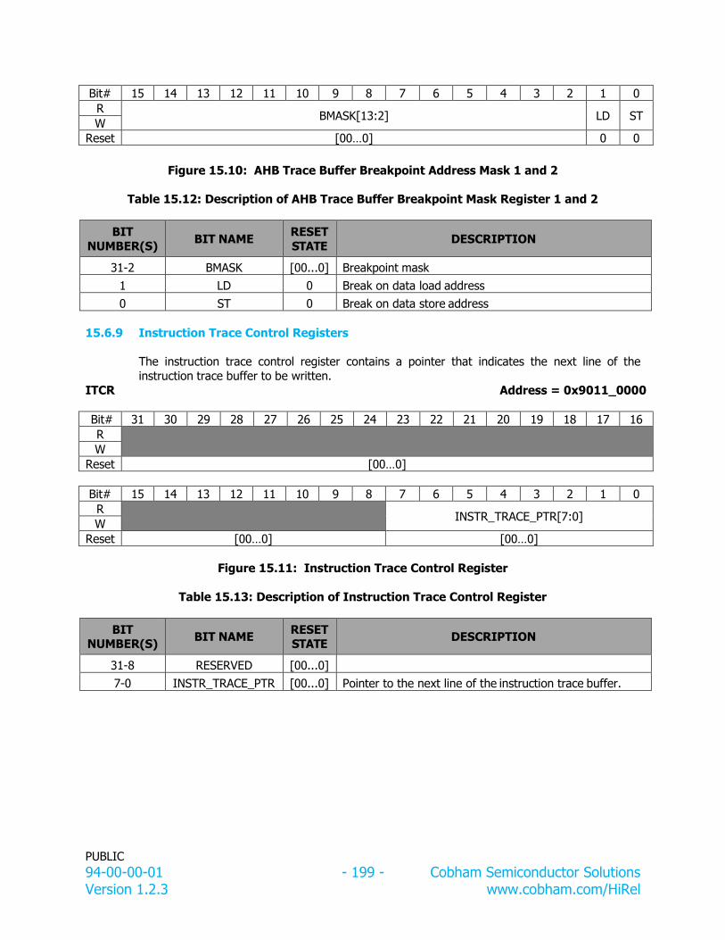
PUBLIC
94-00-00-01 - 199 - Cobham Semiconductor Solutions Version 1.2.3 www.cobham.com/HiRel
Bit# 15 14 13 12 11 10 9 8 7 6 5 4 3 2 1 0
R BMASK[13:2] LD ST
W
Reset [00…0] 0 0
Figure 15.10: AHB Trace Buffer Breakpoint Address Mask 1 and 2
Table 15.12: Description of AHB Trace Buffer Breakpoint Mask Register 1 and 2
BIT
NUMBER(S) BIT NAME
RESET
STATE DESCRIPTION
31-2 BMASK [00...0] Breakpoint mask
1 LD 0 Break on data load address
0 ST 0 Break on data store address
Instruction Trace Control Registers 15.6.9
The instruction trace control register contains a pointer that indicates the next line of the
instruction trace buffer to be written.
ITCR Address = 0x9011_0000
Bit# 31 30 29 28 27 26 25 24 23 22 21 20 19 18 17 16
R
W
Reset [00…0]
Bit# 15 14 13 12 11 10 9 8 7 6 5 4 3 2 1 0
R INSTR_TRACE_PTR[7:0]
W
Reset [00…0] [00…0]
Figure 15.11: Instruction Trace Control Register
Table 15.13: Description of Instruction Trace Control Register
BIT NUMBER(S)
BIT NAME RESET STATE
DESCRIPTION
31-8 RESERVED [00...0]
7-0 INSTR_TRACE_PTR [00...0] Pointer to the next line of the instruction trace buffer.

PUBLIC
94-00-00-01 - 200 - Cobham Semiconductor Solutions Version 1.2.3 www.cobham.com/HiRel
Serial Debug Link Chapter 16:
16.1 Overview
The serial debug link consists of a UART connected to the AHB bus as a master as shown in the Figure 16.1 below. A simple communication protocol is supported to transmit access
parameters and data. Through the communication link, a read or write transfer can be
generated to any address on the AHB bus.
Figure 16.1: Debug UART Block Diagram
16.2 Operation
Transmission Protocol 16.2.1
The debug UART supports simple protocol where commands consist of a control byte, followed by a 32-bit address, followed by optional write data. A Write access does not return any
response, while a read access returns only the read data. Data is sent on 8-bit basis as shown below.
STARTB D0 D1 D2 D3 D4 D5 D6 D7 STOPB
Figure 16.2: Debug UART Data Frame

PUBLIC
94-00-00-01 - 201 - Cobham Semiconductor Solutions Version 1.2.3 www.cobham.com/HiRel
Figure 16.3: Debug UART Commands
Block transfers can be performed by setting the length field to n-1, where n denotes the
number of transferred words. For write accesses, the control byte and address is sent once, followed by the number of data words to be written. The address is automatically incremented
after each data word. For read accesses, the control byte and address is sent once and the
corresponding number of data words is returned.
Baud Rate Generator 16.2.2
The debug UART contains a 18-bit down-counting scaler to generate the desired baud-rate.
The scaler is clocked by the system clock and generates a UART tick each time it underflows. The scaler is reloaded with the value of the UART scaler reload register after each underflow.
The resulting UART tick frequency should be eight times the desired baud-rate.
If not programmed by software, the baud rate will be automatically discovered. This is done by searching for the shortest period between two falling edges of the received data
(corresponding to two bit periods). When three identical two-bit periods have been found, the
corresponding scaler reload value is latched into the reload register, and the Baud Rate Lock (BL) bit is set in the UART Control Register. If the BL bit is reset by software, the baud rate
discovery process is restarted. The baud rate discovery is also restarted when a ‘break’ or framing error is detected by the receiver, allowing the system to change the baud rate from the
external transmitter. For proper baud rate detection, the value 0x55 should be transmitted to
the receiver after reset or after sending a break.
The best scaler value for manually programming the baudrate can be calculated as follows:
scaler = (((system_clk*10)/ (baudrate*8))-5)/10
16.3 Registers The debug UART can be programmed through the registers mapped into APB address space.
Table 16.1: Description of Debug UART Register Address
REGISTER APB ADDRESS
AHB UART Status Register (SDLSTR) 0x80000704
AHB UART Control Register (SDLCTR) 0x80000708

PUBLIC
94-00-00-01 - 202 - Cobham Semiconductor Solutions Version 1.2.3 www.cobham.com/HiRel
REGISTER APB ADDRESS
AHB UART Scaler Register (SDLSCL) 0x8000070C
SDLCTR Address = 0x8000_0704
Bit# 31 30 29 28 27 26 25 24 23 22 21 20 19 18 17 16
R
W
Reset --
Bit# 15 14 13 12 11 10 9 8 7 6 5 4 3 2 1 0
R BL EN
W
Reset [--…-] 0 0
Figure 16.4: Debug UART Control Register
Table 16.2: Description of Debug UART Control Register
BIT
NUMBER(S) BIT NAME
RESET
STATE DESCRIPTION
31-2 RESERVED [--…-] 1 BL 0 Baud Rate Locked
This bit is automatically set when the baud rate is locked.
0 RE 0 Receiver Enable
If set, both the transmitter and receiver are enabled.
SDLSTR Address = 0x8000_0708
Bit# 31 30 29 28 27 26 25 24 23 22 21 20 19 18 17 16
R
W
Reset [--…-]
Bit# 15 14 13 12 11 10 9 8 7 6 5 4 3 2 1 0
R FE OV TH TS DR
W
Reset [--…-] 0 0 0 0 1 1 0
Figure 16.5: Debug UART Status Register
Table 16.3: Description of Debug UART Status Register
BIT
NUMBER(S) BIT NAME
RESET
STATE DESCRIPTION
31-7 RESERVED [--…-] 6 FE 0 Frame Error
Indicates that a frame error was detected.
5 RESERVED 0 4 OV 0 Overrun
Indicates that one or more characters have been lost due

PUBLIC
94-00-00-01 - 203 - Cobham Semiconductor Solutions Version 1.2.3 www.cobham.com/HiRel
BIT
NUMBER(S) BIT NAME
RESET
STATE DESCRIPTION
to overrun.
3 RESERVED 0 2 TH 1 Transmitter Hold Register Empty
Indicates that the transmitter hold register is empty. Read only.
1 TS 1 Transmitter Shift Register Empty
Indicates that the transmitter shift register is empty.
0 DR 0 Data Ready
Indicates that new data has been received by the AHB
master interface.
SDLSCL Address = 0x8000_070C
Bit# 31 30 29 28 27 26 25 24 23 22 21 20 19 18 17 16
R
W
Reset [00…0]
Bit# 15 14 13 12 11 10 9 8 7 6 5 4 3 2 1 0
R SRV[13:0]
W
Reset 00 [00…0]
Figure 16.6: Debug UART Scaler Reload Register
Table 16.4: Description of Debug UART Scaler Reload Register
BIT
NUMBER(S) BIT NAME
RESET
STATE DESCRIPTION
31-14 RESERVED [00...0] 13-0 SRV [00...0] Scaler Reload Value
See Section 15.2.2. The optimum value is: SCALER = ((SYSCLK*10)/baudrate*8))-5/10.

PUBLIC
94-00-00-01 - 204 - Cobham Semiconductor Solutions Version 1.2.3 www.cobham.com/HiRel
JTAG Debug Link Chapter 17:
17.1 Overview
The JTAG debug interface provides access to the AMBA AHB bus through JTAG. The JTAG debug interface implements a simple protocol that translates JTAG instructions to AHB
transfers. Through this link, a read or write transfer can be generated to any address on the
AHB bus.
Figure 17.1: JTAG Debug Link Block Diagram
17.2 Operation
Transmission Protocol 17.2.1
The JTAG Debug link decodes two JTAG instructions and implements two JTAG data registers:
the JTAG Debug Link Command and Address Register and Data Register. A read access is initiated by setting the Write bit, and the SIZE and AHB_ADDRESS fields of the Command and
Address Register and shifting out the data over the JTAG port. The AHB read access is performed and data is ready to be shifted out of the Data Register. Write accesses are
performed by setting the Write bit, and the SIZE and AHB_ADDRESS fields of the Command
and Address Register, followed by shifting in write data into the Data Register. Sequential transfers can be performed by shifting in command and address for the transfer start address
and setting the SEQ bit in Data Register for subsequent accesses. The SEQ bit increments the AHB address for the subsequent access. Sequential transfers should not cross a 1 KB boundary.
Sequential transfers are always word based.
JDLCAR
Bit# 34 33 32
R W SIZE[1:0]
W
Reset 0 00
Bit# 31 30 29 28 27 26 25 24 23 22 21 20 19 18 17 16
R AHB_ADDRESS[31:16]
W
Reset [00…0]
Bit# 15 14 13 12 11 10 9 8 7 6 5 4 3 2 1 0

PUBLIC
94-00-00-01 - 205 - Cobham Semiconductor Solutions Version 1.2.3 www.cobham.com/HiRel
R AHB_ADDRESS[15:0]
W
Reset [00…0]
Figure 17.2: JTAG Debug Link Command and Address Register
Table 17.1: Description of JTAG Debug Link Command and Address Register
BIT NUMBER(S)
BIT NAME RESET STATE
DESCRIPTION
34 W 0 Write 0: Read transfer
1: Write transfer
33-32 SIZE 00 AHB Transfer Size 00: Byte 01: Half word
10: Word
11: Reserved
31-0 AHB_ADDRESS [00...0] AHB Address
JDLDR
Bit# 32
R SQ
W
Reset 0
Bit# 31 30 29 28 27 26 25 24 23 22 21 20 19 18 17 16
R AHB_DATA[31:16]
W
Reset [00…0]
Bit# 15 14 13 12 11 10 9 8 7 6 5 4 3 2 1 0
R AHB_DATA[15:0]
W
Reset [00…0]
Figure 17.3: JTAG Debug Link Data Register
Table 17.2: Description of JTAG Debug Link Data Register
BIT NUMBER(S)
BIT NAME RESET STATE
DESCRIPTION
32 SQ 0 Sequential Transfer
0: Non-sequential transfer 1: When read data is shifted out or write data shifted in,
the subsequent transfer will be to the word address.
31-0 AHB_DATA [00...0] For byte and half-word transfers, data is aligned according to big-endian order where data with address
offset 0 data is placed in MSB bits.

PUBLIC
94-00-00-01 - 206 - Cobham Semiconductor Solutions Version 1.2.3 www.cobham.com/HiRel
Registers 17.2.2
The core does not implement any registers mapped in the AMBA AHB or APB address space.
17.3 Boundary Scan
The JTAG Tap controller supports boundary scan to permit board level interconnect and diagnostic through a JTAG chain. The JTAG TAP controller supports nine instructions: SAMPLE,
PRELOAD, BYPASS, EXTEST, INTEST, Highz, IDCODE, AHBADDR, and AHBDATA. The IDCODE will be read as 0x10699649.
The boundary scan consists of 1 cell bypass, 32 cell IDCODE, 35 cell AHBADDR, 33 cell AHBDATA, and 478 cell scan chain registers. Each register is operated based on the instruction
code loaded the TAP controller. The clock frequency for operating the boundary scan is 10MHz. A Boundary Scan Descriptive Language (BSDL) file providing details on the boundary scan
operations is available at www.aeroflex.com/LEON.

PUBLIC
94-00-00-01 - 207 - Cobham Semiconductor Solutions Version 1.2.3 www.cobham.com/HiRel
CLKGATE Clock Gating Unit Chapter 18:
18.1 Overview
The CLKGATE clock gating unit provides a means to save power by disabling the clock to unutilized core blocks. The unit can enable and disable up to eight individual clock signals or
reset the core state and registers to default.
18.2 Operation The operation of the clock gating unit is controlled through three registers: the unlock, the
clock enables, and the core reset registers. The clock enable register defines if a clock is
enabled or disabled. A ‘1’ in a bit location enables the corresponding clock, while a ‘0’ disables the clock. The core reset register resets each core to a default state. A reset will be generated
as long as the corresponding bit is set to ‘1’. The bits in clock enable and core reset registers can only be written when the corresponding bit in the unlock register is 1. If the a bit in the unlock
register is 0, the corresponding bits in the clock enable and core reset registers cannot be written.
To gate the clock for a core, the following procedure should be applied:
1. Disable the core through software to make sure it does not initialize any AHB accesses. 2. Write 1 to the corresponding bit in the unlock register.
3. Write 1 to the corresponding bit in the core reset register.
4. Write 0 to the corresponding bit in the clock enable register. 5. Write 0 to the corresponding bit in the unlock register.
To enable the clock for a core, the following procedure should be applied
1. Write 1 to the corresponding bit in the unlock register.
2. Write 1 to the corresponding bit in the core reset register.
3. Write 1 to the corresponding bit in the clock enable register. 4. Write 0 to the corresponding bit in the core reset register.
5. Write 0 to the corresponding bit in the unlock register.
The clock gating unit directly controls the clock and reset lines for peripheral units without any
guards in place that check if the peripheral unit is idle. If a peripheral is disabled in the middle of a bus transaction this can lead to a system freeze that requires a full system reset to
resolve. Because of this it is not recommended to disable units via the clock gating unit unless the peripheral being clock gated off is guaranteed to be in idle state.
The cores connected to the clock gating unit are defined in the Table 18.1 below:
Table 18.1: Clocks Controller by CLKGATE Unit
BIT FUNCTIONAL MODE
0 GRSPW SpaceWire link 0
1 GRSPW SpaceWire link 1
2 GRSPW SpaceWire link 2
3 GRSPW SpaceWire link 3
4 CAN core 1 & 2
5 GRETH 10/100 Mbit Ethernet MAC (AHB Clock)
PUBLIC
94-00-00-01 - 208 - Cobham Semiconductor Solutions Version 1.2.3 www.cobham.com/HiRel
6 GRPCI 32-bit PCI Bridge (AHB Clock)
7 GR1553B controller
18.3 Registers Table 18.2 shows the clock gating unit registers. The base address for the registers is
0x80000600.
Table 18.2: Clocks Unit Control Registers
APB ADDRESS FUNCTIONAL MODULE RESET VALUE
0x80000600 Unlock Register 00000000
0x80000604 Clock Enable Register 01111111
0x80000608 Core Reset Register 00000000
NOTE: The clock for the GR1553B is disabled after reset and must be enabled before the unit
can be used.

PUBLIC
94-00-00-01 - 209 - Cobham Semiconductor Solutions Version 1.2.3 www.cobham.com/HiRel
SPI Controller (Only applicable to the Chapter 19:UT700)
19.1 Overview
The SPI controller provides a link between the AMBA APB bus and the Serial Peripheral Interface (SPI) bus. The SPI core is controlled through the APB address space, and can only
work as master. The SPI bus parameters are highly configurable via registers. The controller has configurable word length, bit ordering and clock gap insertion.
Mode Register
Event Register
Mask Register
Com Register
Transmit Register
Slave Register
Receive Register
Mode Register
Mode Register
Mode Register
Mode Register
Mode Register
Mode Register
SYNC
REGISTERS
SPICTRL
SCK
MISO
MOSI
SPISEL
SLVSEL
AMBA
APB
Figure 19.1: SPI Controller Block Diagram
19.2 Operation
SPI Transmission Protocol 19.2.1
The SPI bus is a full-duplex synchronous serial bus. Transmission starts when the clock line SPICLK transitions from its idle state. Data is transferred from the master through the Master-
Output-Slave-Input (SPIMOSI) signal and from the slave through the Master-Input-Slave-
Output (SPIMISO) signal. In a system with only one master and one slave, the Slave Select input of the slave may be always active and the master does not need to have a slave select
output.
During a transmission on the SPI bus, data is either changed or read at a transition of SPICLK.
If data has been read at edge n, data is changed at edge n+1. If data is read at the first transition of SPICLK the bus is said to have clock phase 0 and if data is changed at the first
transition of SPICLK, the bus has clock phase 1. The idle state of SPICLK may be either high or low. If the idle state of SPICLK is low, the bus has clock polarity 0 and if the idle state is high the
clock polarity is 1. The combined values of clock polarity (CPOL) and clock phase (CPHA) determine the mode of the SPI bus. Figure 19.2 shows one byte (0x55) being transferred MSb
first over the SPI bus under the four different modes.
Note: The idle state of the SPIMOSI line is ‘1’ and that CPHA = 0 means that the devices must
have data ready before the first transition of SPICLK. The figure does not include the SPIMISO signal, the behavior of this line is the same as for the SPIMOSI signal.

PUBLIC
94-00-00-01 - 210 - Cobham Semiconductor Solutions Version 1.2.3 www.cobham.com/HiRel
SPICLK
SPIMOSI
SPICLK
SPIMOSI
Mode 2
Mode 3
CPHA=0
CPHA=1
SPICLK
SPIMOSI
SPICLK
SPIMOSI
Mode 0
Mode 1
CPHA=0
CPHA=1
CPOL=0
CPOL=1
Figure 19.2: SPI Transfer of Byte 0x55 in All Modes
Receive and Transmit Queues 19.2.2
The core’s transmit queue consists of the transmit register and the transmit FIFO. The receive
queue consists of the receive register and the receive FIFO. The total number of words that can exist in each queue is thus the FIFO depth plus one.
When the core has one or more free slots in the transmit queue, it asserts the Not full (NF) bit
in the event register. Software may only write to the transmit register when this bit is asserted. When the core has received a word, as defined by word length (LEN) in the Mode register, it
places the data in the receive queue. When the receive queue has one or more elements stored the Event register bit Not empty (NE) will be asserted. The receive register will only
contain valid data if the Not empty bit is asserted and software should not access the receive register unless this bit is set. If the receive queue is full and the core receives a new word, an
overrun condition occurs. The received data will be discarded and the Overrun (OV) bit in the
Event register will be set.
Clock Generation 19.2.3
The core only generates the clock in master mode, the generated frequency depends on the
system clock frequency and the Mode register fields DIV16, FACT, and PM. Without DIV16 the SPICLK frequency is:
𝑆𝐶𝐾𝐹𝑟𝑒𝑞𝑢𝑒𝑛𝑐𝑦 = 𝐴𝑀𝐵𝐴𝐶𝑙𝑜𝑐𝑘𝐹𝑟𝑒𝑞𝑢𝑒𝑛𝑐𝑦
(4 − (2 ∗ 𝐹𝐴𝐶𝑇)) ∗ (𝑃𝑀 + 1)
With DIV16 enabled the frequency of SPICLK is derived through:

PUBLIC
94-00-00-01 - 211 - Cobham Semiconductor Solutions Version 1.2.3 www.cobham.com/HiRel
𝑆𝐶𝐾𝐹𝑟𝑒𝑞𝑢𝑒𝑛𝑐𝑦 = 𝐴𝑀𝐵𝐴𝐶𝑙𝑜𝑐𝑘𝐹𝑟𝑒𝑞𝑢𝑒𝑛𝑐𝑦
(16 ∗ (4 − (2 ∗ 𝐹𝐴𝐶𝑇)) ∗ (𝑃𝑀 + 1)
NOTE: The fields of the Mode register, which includes DIV16, FACT and PM, should not be changed when the core is enabled. If the FACT field is set to 1 the core’s register interface is
compatible with the register interface found in MPC83xx SoCs. If the FACT field is set to 0, the
core can generate an SPICLK clock with higher frequency.
Operation (Master-Only) 19.2.4
Master operation transmits a word when there is data available in the transmit queue. When the transmit queue is empty, the core drives SPICLK to its idle state.
19.3 Registers
The core is programmed through registers mapped into APB address space.
Table 19.1: SPI Controller Registers
Register APB address
Capability register 0x80100100
Mode register 0x80100120
Event register 0x80100124
Mask register 0x80100128
Command register 0x8010012C
Transmit register 0x80100130
Receive register 0x80100134
SPICPR Address = 0x8010_0100
Bit# 31 30 29 28 27 26 25 24 23 22 21 20 19 18 17 16
R SSSZ[7:0] MXL[3:0] SSEN
W
Reset 0x01 0000 000 1
Bit# 15 14 13 12 11 10 9 8 7 6 5 4 3 2 1 0
R FDEPTH[7:0] SR SFT[1:0] REV[4:0]
W
Reset 0x10 1 00 00101
Figure 19.3: SPI Controller Capability Register
Table 19.2: Description of SPI Controller Capability Register
BIT NUMBER(S)
BIT NAME RESET STATE
DESCRIPTION
31-24 SSSZ 0x01 Slave select register size

PUBLIC
94-00-00-01 - 212 - Cobham Semiconductor Solutions Version 1.2.3 www.cobham.com/HiRel
BIT
NUMBER(S) BIT NAME
RESET
STATE DESCRIPTION
If the core has been configured with slave select signals this field contains the number of available signals. This
field is only valid is the SSEN bit 16) is ‘1
23-20 MXL 0000 Max word length
19-17 RESERVED 000
16 SSEN 1 Slave select enable
If the core has a slave select register, and corresponding slave select lines, the value of this field is one. Otherwise
the value of this field is zero.
15-8 FDEPTH 0x10 FIFO depth
This field contains the depth of the core’s internal FIFOs. The number of words the core can store in each queue is
FDEPTH+1, since the transmit and receive registers can
contain one word each.
7 SR 1 SYNCRAM
6-5 SFT 00 Fault tolerance
4-0 REV 00101 Core revision
SPIMD Address = 0x8010_0120
Bit# 31 30 29 28 27 26 25 24 23 22 21 20 19 18 17 16
R LOOP CPOL CPHA DIV16 REVD MS EN LEN[3:0] PM[3:0]
W
Reset 0 0 0 0 0 0 1 0 0000 0000
Bit# 15 14 13 12 11 10 9 8 7 6 5 4 3 2 1 0
R TW ASEL FACT OD CG[4:0] ASELDEL[1:0]
W
Reset 00 0 0 0_0000 00 [00…0]
Figure 19.4: SPI Controller Mode Register
Table 19.3: Description of SPI Controller Mode Register
BIT
NUMBER(S) BIT NAME
RESET
STATE DESCRIPTION
31 RESERVED 0
30 LOOP 0 Loop mode:
When this bit is set, and the core is enabled, the core’s
transmitter and receiver are interconnected and the
core operates in loop- back mode. The core still detects and will be disabled on Multiple-master errors.
29 CPOL 0 Clock polarity:
Determines the polarity (idle state) of the SCK clock.
28 CPHA 0 Clock phase:
PUBLIC
94-00-00-01 - 213 - Cobham Semiconductor Solutions Version 1.2.3 www.cobham.com/HiRel
BIT
NUMBER(S) BIT NAME
RESET
STATE DESCRIPTION
Determines the phase (idle state) of the SCK clock.
27 DIV16 0 Divide by 16:
Divide system clock by 16, see description of PM field
and see Section 19.2.3 on clock generation. This bit has
no significance in slave mode.
26 REVD 0 Reverse data:
When this bit is ‘0’ data is transmitted LSB first, when this
bit is ‘1’ data is transmitted MSB first. This bit affects the
layout of the transmit and receive registers.
25 MS 1 Master/Mode:
1: Operates as a master Read = 1; Write = don’t care
24 EN 0 Enable core:
When this bit is set to ‘1’ the core is enabled. No fields in
the mode register should be changed while the core is
enabled. This bit can be set to ‘0’ by software or by the core if a multiple-master error occurs.
23-20 LEN 0000 Word length:
The value of this field determines the length in bits of a
transfer on the SPI bus. Values are interpreted as:
0b0000 - 32-bit word length 0b0001-0b0010 - Illegal
values
0b0011-0b1111 - Word length is LEN+1, allows words of length 4- 16 bits
The value of this field must never specify a word length
that is greater than the maximum allowed word length specified by the MAXWLEN field in the Capability register.
19-16 PM 0000 Prescale modulus:
This value is used in master mode to divide the system
clock and generate the SPI SCK clock. The value in this
field depends on the value of the FACT bit.
If bit 13 (FACT) is ‘0’:The system clock is divided by
4*(PM+1) if the DIV16 field is ‘0’ and 16*4*(PM+1) if the
DIV16 field is set to ‘1’. The highest SCK frequency is attained when PM is set to 0b0000 and DIV16 to ‘0’, this
configuration gives a SCK frequency that is (system clock)/4. With this setting the core is compatible with the
SPI register interface found in MPC83xx SoCs.
If bit 13 (FACT) is ‘1’: The system clock is divided by
2*(PM+1) if the DIV16 field is ‘0’ and 16*2*(PM+1) if the
DIV16 field is set to ‘1’. The highest SCK frequency is attained when PM is set to 0b0000 and DIV16 to ‘0’, this
configuration gives a SCK frequency that is (system
clock)/2.
In slave mode, the value of this field defines the number
of system clock cycles that the SCK input must be stable
for the core to accept the state of the signal.

PUBLIC
94-00-00-01 - 214 - Cobham Semiconductor Solutions Version 1.2.3 www.cobham.com/HiRel
BIT
NUMBER(S) BIT NAME
RESET
STATE DESCRIPTION
15 TW 0 Three-wire mode (TW) - If this bit is set to ‘1’ the core will operate in 3-wire mode. This bit can only be set if
the TWEN field of the Capability register is set to ‘1’
14 ASEL 0 Automatic slave select (ASEL) - If this bit is set to ‘1’ the
core swaps the contents in the Slave select register with
the contents of the Automatic slave select register when a transfer is started and the core is in master mode.
When the transmit queue is empty, the slave select register will be swapped back. Note that if the core is
disabled (by writing to the core enable bit or due to a
multiple master-error (MME) when a transfer is in progress, the registers may still be swapped when the
core goes idle. This bit can only be set if the ASELA field of the Capability register is set to ‘1’. Also see the
ASELDEL field which can be set to insert a delay between the slave select register swap and the start of a transfer
13 FACT 0 PM factor:
If this bit is 1, the core’s register interface is no longer
compatible with the MPC83xx register interface. The value of this bit affects how the PM field is utilized to
scale the SPI clock. See the description of PM field in this
table above.
12 OD 0 Open drain mode
If this bit is set to ‘0’, all pins are configured for
operation in normal mode. If this bit is set to ‘1’ all pins are set to open drain mode. The implementation of the
core may or may not support open drain mode. If this bit can be set to ‘1’ by writing to this location, the core
supports open drain mode. The pins driven from the slave select register are not affected by the value of this
bit.
11-7 CG 00000 Clock gap:
The value of this field is only significant in master mode.
The core inserts CG SCK clock cycles between each consecutive word. This only applies when the transmit
queue is kept non-empty. After the last word of the transmit queue has been sent, the core goes into an idle
state and continues to transmit data as soon as a new word is written to the transmit register, regardless of the
value in CG. A value of 0b00000 in this field enables
back-to-back transfers.
6-5 ASELDEL 00 Automatic Slave Select Delay
If the core is configured to use automatic slave select
(ASEL field set to ‘1’) the core inserts a delay corresponding to ASELDEL*(SPI SPICLK cycle time)/2
between the swap of the slave select registers and the first toggle of the SPICLK clock. As an example, if this
field is set to “10” the core inserts a delay corresponding to one SPICLK cycle between assigning the Automatic

PUBLIC
94-00-00-01 - 215 - Cobham Semiconductor Solutions Version 1.2.3 www.cobham.com/HiRel
BIT
NUMBER(S) BIT NAME
RESET
STATE DESCRIPTION
slave select register to the Slave select register and toggling SPICLK for the first time in the transfer. This
field can only be set if the ASELA field of the Capability register is set to ‘1’.
4-0 RESERVED [00…0]
SPIER Address = 0x8010_0124
Bit# 31 30 29 28 27 26 25 24 23 22 21 20 19 18 17 16
R TIP
W
Reset 0 [00…0]
Bit# 15 14 13 12 11 10 9 8 7 6 5 4 3 2 1 0
R LT
OV UN NE NF
W
Reset 0 0 0 0 0 0 0 0 [00…0]
Figure 19.5: SPI Controller Event Register
Table 19.4: Description of SPI Controller Event Register
BIT
NUMBER(S) BIT NAME
RESET
STATE DESCRIPTION
31 TIP 0 Transfer in progress LF (Line Feed). This bit is ‘1’ when
the core has a transfer in progress. Writes have no effect.
30-15 RESERVED [00...0] RESERVED
Read as zero and should be written to zero to ensure
forward compatibility.
14 LT 0 Last character LF. This bit is set when a transfer
completes if the transmit queue is empty and the LST bit in the Command register has been written. This bit is
cleared by writing ‘1’, writes of ‘0’ have no effect.
13 RESERVED 0 RESERVED LF. Read as zero and should be written to zero to ensure forward compatibility.
12 OV 0 Overrun LF. This bit gets set when the receive queue is
full and the core receives new data. The core continues
communicating over the SPI bus, but discards the new data. This bit is cleared by writing ‘1’, writes of ‘0’ have
no effect.
11 UN 0 Underrun (UN) - This bit is only set when the core is
operating in slave mode. The bit is set if the core
transmit queue is empty when a master initiates a transfer. When this happens the core responds with a
word where all bits are set to ‘1’. This bit is cleared by writing ‘1’, writes of ‘0’ have no effect.

PUBLIC
94-00-00-01 - 216 - Cobham Semiconductor Solutions Version 1.2.3 www.cobham.com/HiRel
BIT
NUMBER(S) BIT NAME
RESET
STATE DESCRIPTION
10 RESERVED 0
9 NE 0 Not empty LF. This bit is set when the receive queue contains one or more elements. It is cleared
automatically by the core; writes have no effect.
8 NF 0 Not full LF. This bit is set when the transmit queue has
room for one or more words. It is cleared automatically by the core when the queue is full; writes have no effect.
7-0 RESERVED [00...0] RESERVED LF. Read as zero and should be written to
zero to ensure forward compatibility.
SPIMR Address = 0x8010_0128
Bit# 31 30 29 28 27 26 25 24 23 22 21 20 19 18 17 16
R TIPE
W
Reset 0 [00…0]
Bit# 15 14 13 12 11 10 9 8 7 6 5 4 3 2 1 0
R LTE
OVE UNE MMEE NEE NFE
W
Reset 0 0 0 0 0 0 0 0 [00…0]
Figure 19.6: SPI Controller Mask Register
Table 19.5: Description of SPI Controller Mask Register
BIT
NUMBER(S) BIT NAME
RESET
STATE DESCRIPTION
31 TIPE 0 Transfer in progress enable When this bit is set ,the core generates an interrupt when
the TIP bit in the Event register transitions from ‘0’ to ‘1’.
30-15 RESERVED [00...0] RESERVED
Read as zero and should be written to zero to ensure forward compatibility.
14 LTE 0 Last character enable
When this bit is set, the core generates an interrupt when
the LT bit in the Event register transitions from ‘0’ to ‘1’.
13 RESERVED 0 RESERVED
Read as zero and should be written to zero to ensure
forward compatibility.
12 OVE 0 Overrun enable
When this bit is set ,the core generates an interrupt when the OV bit in the Event register transitions from ‘0’ to ‘1’.
11 UNE 0 Underrun enable
When this bit is set, the core generates an interrupt when
the UN bit in the Event register transitions from ‘0’ to ‘1’.

PUBLIC
94-00-00-01 - 217 - Cobham Semiconductor Solutions Version 1.2.3 www.cobham.com/HiRel
BIT
NUMBER(S) BIT NAME
RESET
STATE DESCRIPTION
10 MMEE 0 Multiple-master error enable
When this bit is set, the core generates an interrupt when
the MME bit in the Event register transitions from ‘0’ to ‘1’.
9 NEE 0 Not empty enable
When this bit is set, the core generates an interrupt when
the NE bit in the Event register transitions from ‘0’ to ‘1’.
8 NFE 0 Not full enable
When this bit is set, the core generates an interrupt when
the NF bit in the Event register transitions from ‘0’ to ‘1’.
7-0 RESERVED 0 RESERVED
Read as zero and should be written to zero to ensure forward compatibility.
SPICCR Address = 0x8010_012C
Bit# 31 30 29 28 27 26 25 24 23 22 21 20 19 18 17 16
R LST
W
Reset [00…0] 0 [00…0]
Bit# 15 14 13 12 11 10 9 8 7 6 5 4 3 2 1 0
R
W
Reset [00…0]
Figure 19.7: SPI Controller Command Register
Table 19.6: Description of SPI Controller Command Register
BIT NUMBER(S)
BIT NAME RESET STATE
DESCRIPTION
31-23 RESERVED [00…0] RESERVED
Read as zero and should be written to zero to ensure
forward compatibility.
22 LST 0 Last
After this bit has been written to ‘1’ the core sets the
Event register bit LT when a character has been
transmitted and the transmit queue is empty. If the core is operating in 3-wire mode, the Event register bit is set
when the whole transfer has completed. This bit is automatically cleared when the Event register bit has
been set and is always read as zero.
21-0 RESERVED [00…0] RESERVED
Read as zero and should be written to zero to ensure forward compatibility.

PUBLIC
94-00-00-01 - 218 - Cobham Semiconductor Solutions Version 1.2.3 www.cobham.com/HiRel
SPITR Address = 0x8010_0130
Bit# 31 30 29 28 27 26 25 24 23 22 21 20 19 18 17 16
R TDATA[31:16]
W
Reset [00…0]
Bit# 15 14 13 12 11 10 9 8 7 6 5 4 3 2 1 0
R TDATA[15:0]
W
Reset [00…0]
Figure 19.8: SPI Controller Transmit Register
Table 19.7: Description of SPI Controller Transmit Register
BIT NUMBER(S)
BIT NAME RESET STATE
DESCRIPTION
31-0 TDATA [00…0] Transmit data (TDATA) - Writing a word into this register
places the word in the transmit queue. This register only
reacts to writes if the Not full (NF) bit in the Event register is set. The layout of this register depends on the
value of the REV field in the Mode register:
Rev = ‘0’: The word to transmit should be written with its
least significant bit at bit 0.
Rev = ‘1’: The word to transmit should be written with its
most significant bit at bit 31.
SPIRR Address = 0x8010_0134
Bit# 31 30 29 28 27 26 25 24 23 22 21 20 19 18 17 16
R RDATA[31:16]
W
Reset [--…-]
Bit# 15 14 13 12 11 10 9 8 7 6 5 4 3 2 1 0
R RDATA[15:0]
W
Reset [--…-]
Figure 19.9: SPI Controller Transmit Register
Table 19.8: Description of SPI Controller Transmit Register
BIT
NUMBER(S) BIT NAME
RESET
STATE DESCRIPTION
31-0 RDATA [--…-] Receive data (RDATA) - This register contains valid
receive data when the Not empty (NE) bit of the Event
register is set. The placement of the received word

PUBLIC
94-00-00-01 - 219 - Cobham Semiconductor Solutions Version 1.2.3 www.cobham.com/HiRel
BIT
NUMBER(S) BIT NAME
RESET
STATE DESCRIPTION
depends on the Mode register fields LEN and REV:
For LEN = 0b0000 - The data is placed with its MSb in
bit
31 and its LSb in bit 0.
For other lengths and REV = ‘0’ - The data is placed
with its MSB in bit 15.
For other lengths and REV = ‘1’ - The data is placed with its LSB in bit 16.
To illustrate this, a transfer of a word with eight bits
(LEN = 7) that are all set to one have the following placement:
REV = ‘0’ - 0x0000FF00
REV = ‘1’ - 0x00FF0000

PUBLIC
94-00-00-01 - 220 - Cobham Semiconductor Solutions Version 1.2.3 www.cobham.com/HiRel
Dual Redundant MTL-STD-1553B Interface Chapter 20:(GR1553B) (Only applicable to the UT700)
20.1 Overview
This interface core connects the AMBA AHB/APB bus to a dual redundant MIL-STD-1553B bus and can operate as a Bus Controller, Remote Terminal or Bus Monitor.
MIL-STD-1553B is a bus standard for transferring data between up to 32 devices over a shared (typically dual-redundant) differential wire. The bus is designed for predictable real-time
behavior and fault-tolerance. The raw bus data rate is fixed at 1 Mbit/s, giving a maximum
payload data rate of around 770 Kbit/s.
One of the terminals on the bus is the Bus Controller (BC) which controls all traffic on the bus. The other terminals are Remote Terminals (RTs), which act on commands issued by the bus
controller. Each RT is assigned a unique address between 0-30. In addition, the bus may have
passive Bus Monitors (BMs) connected.
There are 5 possible data transfer commands on the MIL-STD-1553 bus:
1. BC-to-RT transfer (“receive”) 2. RT-to-BC transfer (“transmit”)
3. RT-to-RT transfer
4. Broadcast BC-to-RTs 5. Broadcast RT-to-RTs
Each transfer can contain 1-32 data words, each16 bits wide.
The bus controller can also send “mode codes” to the RTs to perform administrative tasks such as time synchronization, and reading out terminal status.
20.2 Electrical Interface
The core is connected to the MIL-STD-1553B bus wire through single or dual transceivers, isolation transformers and transformer or stub couplers as shown in Figure 20.1.If single-
redundancy is used, the unused bus receives P/N signals should be tied both-high or both-low. The transmit/receive enables may be inverted on some transceivers. See the standard and the
respective component’s data sheets for more information on the electrical connection.

PUBLIC
94-00-00-01 - 221 - Cobham Semiconductor Solutions Version 1.2.3 www.cobham.com/HiRel
Figure 20.1: Interface between Core and MIL-STD-1553B Bus (Dual-Redundant, transformer Coupled)
20.3 Operation
Operation Modes 20.3.1
The core contains three separate control units for the Bus Controller, Remote Terminal and Bus
Monitor handling, with a shared 1553 codec. The operating mode of the core is controlled by
starting and stopping of these units via register writes. At power-up, the GR1553B clock is disabled rendering the BC and RT inoperative.
The BC and RT parts of the core cannot be active on the 1553 bus at the same time. While the
BC is running or suspended, only the BC (and possibly BM) has access to the 1553 bus, and the RT can only receive and respond to commands when both the BC schedules are completely
stopped (not running or even suspended).
The Bus Monitor, however, is only listening on the codec receivers and operates regardless of the
enabled/disabled state of the other two parts.
Register Interface 20.3.2
The core is configured and controlled through control registers accessed over the APB bus. Each
of the BC, RT, and BM parts has a separate set of registers, plus there is a small set of shared registers.
Some of the control register fields for the RT are protected using a ‘key’, a field in the same
register that has to be written with a certain value for the write to take effect. The purpose of
the keys is to give RT/BM designers a way to ensure that the software can not interfere with the bus traffic by enabling the BC or changing the RT address. If the software is built without
knowledge of the key to a certain register, it is very unlikely that it will accidentally perform a write with the correct key to that control register.
Interrupting 20.3.3
The core has one interrupt output which can be generated from several different source events. Which events should cause an interrupt can be controlled through the IRQ Enable Mask
register.
MIL-STD-1553 Codec 20.3.4
The core’s internal codec receives and transmits data words on the 1553 bus and generates and
checks sync patterns and parity. Loop-back checking logic checks that each transmitted word is also seen on the receive inputs. If the transmitted word is not echoed back, the transmitter
stops and signals an error condition which is then reported back to the user.
20.4 Bus Controller Operation
Overview 20.4.1

PUBLIC
94-00-00-01 - 222 - Cobham Semiconductor Solutions Version 1.2.3 www.cobham.com/HiRel
When operating as Bus Controller, the core controls message transactions on the MIL-STD-1553
bus.
This mode works based on a scheduled transfer list concept. The software sets up a sequence of transfer descriptors and branches, data buffers for send and receive data and an IRQ pointer
ring buffer in the available memory space. When the schedule is started (through a BC action
register write), the core processes the list, performs the transfers one after another and writes resulting status into the transfer list and incoming data into the corresponding buffers.
Timing Control 20.4.2
When operating as Bus Controller, the core controls message transactions on the MIL-STD-1553
bus.
In each transfer descriptor in the schedule is a “slot time” field. If the scheduled transfer
finishes sooner than its slot time, the core pauses the remaining time before scheduling the next command. This allows the user to accurately control the message timing during a
communication frame.
If the transfer uses more than its slot time, the overshooting time will be subtracted from the
following command’s time slot. The following command may in turn borrow time from the following command and so on. The core can keep track of up to one second of borrowed time,
and will not insert pauses again until the balance is positive, except for inter-message gaps and pauses that the standard requires.
If you wish to execute the schedule as fast as possible you can set all slot times in the schedule to zero. If you want to group a number of transfers you can move all the slot time to the last
transfer.
The schedule can be stopped or suspended by writing into the BC action register. When
suspended, the schedule’s time will still be accounted so that the schedule timing will still be correct when the schedule is resumed. When stopped, on the other hand, the schedule’s timers
will be reset.
Bus Selection 20.4.3
Each transfer descriptor has a bus selection bit that allows you to control on which one of the
two redundant buses (‘0’ for bus A, ‘1’ for bus B) the transfer occurs.
Another way to control the bus usage is through the per-RT bus swap register which has one register bit for each RT address. Writing a ‘1’ to a bit in the register inverts the meaning of the
bus selection bit for all transfers to the corresponding RT, so ‘0’ now means bus ‘B’ and ‘1’
means bus ‘A’. This allows you to switch all transfers to one or a set of RTs over to the other bus with a single register write and without having to modify any descriptors.
The hardware determines which bus to use by taking the exclusive-or of the bus swap register
bit and the bus selection bit. Normally, it only makes sense to use one of these two methods
for each RT, either the bus selection bit is always zero and the swap register is used, or the swap register bit is always zero and the bus selection bit is used.
If the bus swap register is used for bus selection, the store-bus descriptor bit can be enabled to
automatically update the register depending on transfer outcome. If the transfer succeeded on

PUBLIC
94-00-00-01 - 223 - Cobham Semiconductor Solutions Version 1.2.3 www.cobham.com/HiRel
bus A, the bus swap register bit is set to ‘0’, if it succeeds on bus B, the swap register bit is set
to ‘1’. If the transfer fails, the bus swap register is set to the opposite value.
Secondary Transfer List 20.4.4
The core can be set up with a secondary “asynchronous” transfer list with the same format as
the ordinary schedule. This transfer list can be commanded to start at any time during the ordinary schedule. While the core is waiting for a scheduled command’s slot time to finish, it
checks if the next asynchronous transfer’s slot time is lower than the remaining sleep time. In that case, the asynchronous command will be scheduled.
If the asynchronous command doesn’t finish in time, time will be borrowed from the next command in the ordinary schedule. In order to not disturb the ordinary schedule, the slot time
for the asynchronous messages must be set to pessimistic values.
The exclusive bit in the transfer descriptor can be set if one does not want an asynchronous command scheduled during the sleep time following the transfer.
Asynchronous messages will not be scheduled while the schedule is waiting for a sync pulse or the schedule is suspended and the current slot time has expired since it is not known when the
next scheduled command will start.
Interrupt Generation 20.4.5
Each command in the transfer schedule can be set to generate an interrupt after certain
transfers have completed, with or without error. Invalid command descriptors always generate interrupts and stop the schedule. Before a transfer-triggered interrupt is generated, the address
to the corresponding descriptor is written into the BC transfer-triggered IRQ ring buffer and the
BC Transfer-triggered IRQ Ring Position Register is incremented. A separate error-interrupt signals DMA errors. If a DMA error occurs when reading/writing
descriptors, the executing schedule will be suspended. DMA errors in data buffers cause the corresponding transfer to fail with an error code (see Table 20.4).
Whether any of these interrupt events actually cause an interrupt request on the AMBA bus is controlled by the IRQ Mask Register setting.
Transfer List Format 20.4.6
The BC’s transfer list is an array of transfer descriptors mixed with branches as shown in Table 20.3. Each entry has to be aligned to start on a 128-bit (16-byte) boundary. The two unused
words in the branch case are free to be used by software to store arbitrary data.
Table 20.1: GR1553B Transfer Descriptor Format
Offset Value for transfer descriptor DMA R/W Value for branch DMA R/W
0x00 Transfer descriptor word 0 R Condition word R
0x04 Transfer descriptor word 1 R Jump address, 128-bit aligned
R
0x08 Data buffer pointer, 16-bit aligned.
For write buffers, if bit 0 is set the received data is discarded and the pointer
is ignored. This can be used for RT-to-RT transfers where the BC is not interested
in the data transferred.
R Unused -
0x0C Result word, written by core W Unused -

PUBLIC
94-00-00-01 - 224 - Cobham Semiconductor Solutions Version 1.2.3 www.cobham.com/HiRel
GRBCTDW0 Offset = 0x00
Bit# 31 30 29 28 27 26 25 24 23 22 21 20 19 18 17 16
R DID WTRIG EXCL IRQE IRQN SUSE SUSN RETMD[1:0] NRET[2:0] STBUS GAP
W
Reset 0 0 0 0 0 0 0 00 000 0 0 0
Bit# 15 14 13 12 11 10 9 8 7 6 5 4 3 2 1 0
R STIME[15:0]
W
Reset [00…0]
Figure 20.2: GR1553B BC Transfer Descriptor Word 0
Table 20.2: Description of GR1553B BC Transfer Descriptor Word 0
BIT
NUMBER(S) BIT NAME
RESET
STATE DESCRIPTION
31 DID 0 Must be 0 to identify as descriptor
30 WTRIG 0 Wait for external trigger (WTRIG)
29 EXCL 0 Exclusive time slot - Do not schedule asynchronous messages
28 IRQE 0 IRQ after transfer on Error
27 IRQN 0 IRQ normally - Always interrupts after transfer
26 SUSE 0 Suspend on Error - Suspends the schedule (or stops the asynchronous transfer list) on error
25 SUSN 0 Suspend normally - Always suspends after transfer
24-23 RETMD 00 Retry mode 00 - Retry on same bus only. 01 - Retry alternating on both buses
10: Retry first on same bus, then on alternating bus.
11 - RESERVED, do not use
22-20 NRET 000 Number of retries - Number of automatic retries per bus
The total number of tries (including the first attempt) is NRET+1 for RETMD=00, 2 x (NRET+1) for
RETMD=01/10
19 STBUS 0 Store bus - If the transfer succeeds and this bit is set, store the bus on which the transfer succeeded (0 for bus
A, 1 for bus B) into the per-RT bus swap register. If the
transfer fails and this bit is set, store the opposite bus instead.
18 GAP 0 Extended inter-message gap - If set, adds an additional amount of gap time, corresponding to the RTTO field,
after the transfer
17-16 RESERVED 0 RESERVED- Set to 0 for forward compatibility
15-0 STIME [00...0] Slot time - Allocated time in 4 microsecond units, remaining time after transfer will insert delay

PUBLIC
94-00-00-01 - 225 - Cobham Semiconductor Solutions Version 1.2.3 www.cobham.com/HiRel
GRBCTDW1 Offset = 0x04
Bit# 31 30 29 28 27 26 25 24 23 22 21 20 19 18 17 16
R DUM BUS RTTO[3:0] RTAD2[4:0] RTSA2[4:0]
W
Reset 0 0 0000 0_0000 0_0000
Bit# 15 14 13 12 11 10 9 8 7 6 5 4 3 2 1 0
R RTAD1[4:0] TR RTSA1[4:0] WCMC[4:0]
W
Reset 0_0000 0 0_0000 0_0000
Figure 20.3: GR1553B BC Transfer Descriptor Word 1
Table 20.3: Description of GR1553B BC Transfer Descriptor Word 1
BIT
NUMBER(S) BIT NAME
RESET
STATE DESCRIPTION
31 DUM 0 Dummy transfer
If set to ‘1’ no bus traffic is generated and transfer “succeeds” immediately
For dummy transfers, the EXCL, IRQN, SUSN, STBUS,
GAP, STIME settings are still in effect, other bits and the data buffer pointer are ignored.
30 BUS 0 Bus selection
Bus to use for transfer, 0 - Bus A, 1 - Bus B
29-26 RTTO 0000 RT Timeout
Extra RT status word timeout above nominal in units of 4 us (0000-14 us, 1111 -74 us).
NOTE: This extra time is also used as extra inter-
message gap time if the GAP bit is set.
25-21 RTAD2 00000 Second RT Address for RT-to-RT transfer See Table 175
for details on how to setup
RTAD1, RTSA1, RTAD2, RTSA2, WCMC, TR for different transfer types.
20-16 RTSA2 00000 Second RT Sub-address for RT-to-RT transfer See Table
178 for details on how to setup RTAD1, RTSA1, RTAD2, RTSA2, WCMC, TR for different
transfer types.
15-11 RTAD1 00000 RT Address
10 TR 0 Transmit/receive
NOTE: Bits 15:0 correspond to the (first) command word on the 1553 bus
9-5 RTSA1 00000 RT Sub-address
4-0 WCMC 00000 Word count/Mode code

PUBLIC
94-00-00-01 - 226 - Cobham Semiconductor Solutions Version 1.2.3 www.cobham.com/HiRel
GRBCTDRW Offset = 0x0C
Bit# 31 30 29 28 27 26 25 24 23 22 21 20 19 18 17 16
R 0 RT2ST[7:0]
W
Reset 0 [00…0] [00…0]
Bit# 15 14 13 12 11 10 9 8 7 6 5 4 3 2 1 0
R RTST[7:0] RETCNT[3:0] TFRST[2:0]
W
Reset [00…0] 0000 0 000
Figure 20.4: GR1553B BC Transfer Descriptor Result Word
Table 20.4: Description of GR1553B BC Transfer Descriptor Result Word
BIT
NUMBER(S) BIT NAME
RESET
STATE DESCRIPTION
31 0 Always written as 0
30-24 RESERVED [00...0] RESERVED
23-16 RT2ST [00...0] RT 2 Status Bits
Status bits from receiving RT in RT-to-RT transfer, otherwise 0 Same bit pattern as for RTST below
15-8 RTST [00...0] RT Status Bits
Status bits from RT (transmitting RT in RT-to-RT transfer) 15 - Message error,
14 - Instrumentation bit or RESERVED bit set, 13 - Service request,
12 - Broadcast command received,
11 - Busy bit, 10 - Subsystem flag,
9 - Dynamic bus control acceptance, 8 - Terminal flag
7-4 RETCNT [00...0] Retry count
Number of retries performed
3 RESERVED 0 RESERVED
2-0 TFRST 000 Transfer status
Outcome of last try: 000 - Success (or dummy bit was set)
001 - RT did not respond (transmitting RT in RT-to-RT
transfer) 010 - Receiving RT of RT-to-RT transfer did not respond
011 - A responding RT:s status word had message error, busy, instrumentation or RESERVED bit set (*)
100 - Protocol error (improperly timed data words, decoder
error, wrong number of data words)
101 - The transfer descriptor was invalid 110 - Data buffer DMA timeout or error response
111 - Transfer aborted due to loop back check failure

PUBLIC
94-00-00-01 - 227 - Cobham Semiconductor Solutions Version 1.2.3 www.cobham.com/HiRel
* Error code 011 is issued only when the number of data words matches the success case,
otherwise code 100 is used. Error code 011 can be issued for a correctly executed "transmits last command" or "transmit last status word" mode code since these commands does not reset
the status word.
Table 20.5: GR1553B BC Transfer Configuration Bits for Different Transfer Types
TRANSFE
R TYPE
RTAD1 (15:11)
RTSA1 (9:5)
RTAD2 (25:21)
RTSA2 (20:16)
WCMC (4:0)
TR (10)
DATA
BUFFER DIRECTION
Data, BC-
to-RT
RT address
(0-30)
RT sub-addr
(1-30)
Don’t care 0 Word
count (0 for 32)
0 Read
(2-64 bytes)
Data, RT-
to-BC
RT address
(0-30)
RT sub-addr
(1-30)
Don’t care 0 Word
count (0 for 32)
1 Write
(2-64 bytes)
Data, RT-
to-RT
Recv-RT addr
(0-30)
Recv-RT
subad. (1-30)
Xmit-RT addr
(0-30)
Xmit-RT
subad. (1-30)
Word
count (0 for 32)
0 Write
(2-64 bytes)
Mode, no
data
RT address
(0-30)
0 or 31 (*) Don’t care Don’t
care
Mode
code (0-8)
1 Unused
Mode, RT-to-BC
RT address (0-30)
0 or 31 (*) Don’t care Don’t care
Mode code (16/
18/19)
1 Write (2 bytes)
Mode, BC-to-RT
RT address (0-30)
0 or 31 (*) Don’t care Don’t care
Mode code (17/
20/21)
0 Read (2 bytes)
Broadcast Data, BC-
to-RTs
31 RTs sub- addr (1-30)
Don’t care 0 Word count
(0 for 32)
0 Read (2-64 bytes)
Broadcast Data, RT-
to-RTs
31 Recv-RTs subad.
(1-30)
Xmit-RT addr (0-30)
Xmit-RT subad.
(1-30)
Word count
(0 for 32)
0 Write (2-64 bytes)
Broadcast Mode, no
data
31 0 or 31 (*) Don’t care Don’t care
Mode code (1,
3-8)
1 Unused
Broadcast Mode, BC-
to-RT
31 0 or 31 (*) Don’t care Don’t care
Mode code (17/
20/21)
0 Read (2 bytes)
(*) The standard allows using either of sub-address 0 or 31 for mode commands.
The branch condition word is formed as shown in Table 20.6.
GRBCCW Offset = 0x00
Bit# 31 30 29 28 27 26 25 24 23 22 21 20 19 18 17 16
R 1 IRQC ACT MODE RT2CC[7:0]
W
Reset 0 0000 0 0 0 [00…0]

PUBLIC
94-00-00-01 - 228 - Cobham Semiconductor Solutions Version 1.2.3 www.cobham.com/HiRel
Bit# 15 14 13 12 11 10 9 8 7 6 5 4 3 2 1 0
R RTCC[7:0] STCC[7:0]
W
Reset [00…0] [00…0]
Figure 20.5: GR1553B Branch Condition Word
Table 20.6: Description of GR1553B Branch Condition Word
BIT
NUMBER(S) BIT NAME
RESET
STATE DESCRIPTION
31 -- 0 Must be 1 to identify as branch
30-27 RESERVED 0000 RESERVED – Set to 0
26 IRQC 0 Interrupt if condition met
25 ACT 0 Action
What to do if condition is met, 0 – Suspend schedule, 1 – Jump
24 MODE 0 Logic mode: 0 = Or mode (any bit set in RT2CC, RTCC is set in RT2ST,
RTST, or result is in STCC mask)
1 – And mode (all bits set in RT2CC,RTCC are set in RT2ST, RTST and result is in STCC mask)
23-16 RT2CC [00…0] RT 2 Condition Code
Mask with bits corresponding to RT2ST in result word of last transfer
15-8 RTCC [00…0] RT Condition Code
Mask with bits corresponding to RTST in result word of last transfer
7:0 STCC [00…0] Status Condition Code Mask with bits corresponding to status value of last
transfer
NOTE: You can get a constant true condition by setting MODE=0 and STCC=0xFF, and a
constant false condition by setting STCC=0x00. 0x800000FF can thus be used as an end-of-list
marker.
20.5 Remote Terminal Operation
Overview 20.5.1
When operating as Remote Terminal, the core acts as a slave on the MIL-STD-1553B bus. It
listens for requests to its own RT address (or broadcast transfers), checks whether they are configured as legal and, if legal, performs the corresponding transfer or, if illegal, sets the
message error flag in the status word. Legality is controlled by the sub-address control word for data transfers and by the mode code control register for mode codes.
To start the RT, set up the sub-address table and log ring buffer, and then write the address and RT enable bit in the RT Configuration Register.

PUBLIC
94-00-00-01 - 229 - Cobham Semiconductor Solutions Version 1.2.3 www.cobham.com/HiRel
Data Transfer Handling 20.5.2
The Remote Terminal mode uses a three-level structure to handle data transfer DMA. The top
level is a sub-address table, where each sub-address has a sub-address control word, and pointers to a transmit descriptor and a receive descriptor. Each descriptor in turn contains a
descriptor control/status word, pointer to a data buffer and a pointer to a next descriptor,
forming a linked list or ring of descriptors. Data buffers can reside anywhere in memory with 16-bit alignment.
When the RT receives a data transfer request, it checks in the sub-address table that the
request is legal. If it is legal, the transfer is then performed with DMA to or from the corresponding data buffer. After a data transfer, the descriptor’s control/status word is updated
with success or failure status and the sub-address table pointer is changed to point to the next
descriptor.
If logging is enabled, a log entry will be written into a log ring buffer area. A transfer-triggered IRQ may also be enabled. To identify which transfer caused the interrupt, the RT Event Log IRQ
Position points to the corresponding log entry. For that reason, logging must be enabled in
order to enable interrupts.
If a request is legal, but cannot be fulfilled, either because there is no valid descriptor ready or because the data cannot be accessed within the required response time, the core signals a RT
table access error interrupt and not respond to the request. Optionally, the terminal flag status bit can be automatically set on these error conditions.
Figure 20.6: RT Sub Address Data Structure Example Diagram
Mode Codes 20.5.3
Any of the MIL-STD-1553B mode codes that are legal and should be logged and interrupted are controlled by the RT Mode Code Control register. As for data transfers, to enable interrupts, you
must also enable logging. Inhibit mode codes are controlled by the same fields as their non-inhibit counterpart and mode codes that can be broadcast have two separate fields to control
the broadcast and non-broadcast variants. The different mode codes and the corresponding
action taken by the RT are tabulated below. Some mode codes do not have a built-in action, so

PUBLIC
94-00-00-01 - 230 - Cobham Semiconductor Solutions Version 1.2.3 www.cobham.com/HiRel
they need to be implemented in software if desired. The relation between each mode code to
the fields in the RT Mode Code control register is shown.
Table 20.7: RT Mode Code
Mode Code Description
Built-in action, if mode code is enabled
Can log/IRQ
Enabled
after reset
Ctrl
reg bits
0 00000 Dynamic bus
control
If the DBCA bit is set in the RT Bus
Status register, a Dynamic Bus Control Acceptance response is sent.
Yes No 17:16
1 00001 Synchronize The time field in the RT sync register
is updated. The output rtsync is pulsed high one AMBA cycle.
Yes Yes 3:0
2 00010 Transmit status word
Transmits the RT:s status word Enabled always, cannot be logged or
disabled.
No Yes -
3 00011 Initiate self-test No built-in action Yes No 21:18
4 00100 Transmitter shutdown
The RT stops responding to commands on the other bus (not the
bus on which this command was given).
Yes Yes 11:8
5 00101 Override
transmitter shutdown
Removes the effect of an earlier
transmitter shutdown mode code received on the same bus
Yes Yes 11:8
6 00110 Inhibit terminal
flag
Masks the terminal flag of the sent RT
status words
Yes No 25:22
7 00111 Override inhibit
terminal flag
Removes the effect of an earlier
inhibit terminal flag mode code.
Yes No
25:22
8 01000 Reset remote terminal
The fail-safe timers, transmitter shutdown and inhabit terminal flag
inhibit status are reset. The Terminal Flag and Service Request bits in the
RT Bus Status register are cleared.
The extreset output is pulsed high one AMBA cycle.
Yes No 29:26
16 10000 Transmit vector
word
Responds with vector word from RT
Status Words Register
Yes No 13:12
17 10001 Synchronize with
data word
The time and data fields in the RT
sync register are updated. The rtsync output is pulsed high one AMBA cycle
Yes Yes 7:4
18 10010 Transmit last
command
Transmits the last command sent to
the RT. Enabled always, cannot be logged or disabled.
No Yes -
19 10011 Transmit BIT
word
Responds with BIT word from RT
Status Words Register
Yes No 15:14
20 10100 Selected
transmitter
shutdown
No built-in action No No -
21 10101 Override
selected
transmitter
No built-in action No No -

PUBLIC
94-00-00-01 - 231 - Cobham Semiconductor Solutions Version 1.2.3 www.cobham.com/HiRel
Mode Code Description
Built-in action, if mode code is enabled
Can log/IRQ
Enabled
after reset
Ctrl
reg bits
shutdown
Event Log 20.5.4
The event log is a ring of 32-bit entries, each entry having the format given in Table 20.8.
NOTE: For data transfers, bits 23-0 in the event log are identical to bits 23-0 in the descriptor status word.
Bit# 31 30 29 28 27 26 25 24 23 22 21 20 19 18 17 16
R IRQSR TYPE[1:0] SAMC[4:0] TIMEL[13:6]
W
Reset 0 00 0_0000 [00…0]
Bit# 15 14 13 12 11 10 9 8 7 6 5 4 3 2 1 0
R TIMEL[5:0] BC SZ[5:0] TRES[2:0]
W
Reset [00…0] 0 [00…0] 000
Figure 20.7: GR1553B RT Event Log Entry Format
Table 20.8: Description of GR1553B RT Event Log Entry Format
BIT NUMBER(S)
BIT NAME RESET STATE
DESCRIPTION
31 IRQSRC 0 IRQ Source Set to ‘1’ if this transfer caused an interrupt
30-29 TYPE 00 Transfer type
00 – Transmit data, 01 – Receive data, 10 – Mode code
28-24 SAMC 00000 Sub-address / Mode code If TYPE=00/01 this is the transfer sub-address, If TYPE=10, this is the mode code
23-10 TIMEL [00…0] Low 14 bits of time tag counter.
9 BC 0 Broadcast Set to 1 if request was to the broadcast address
8-3 SZ [00…0] Transfer size
Count in 16-bit words (0-32)
2-0 TRES 000 Transfer result 000 = Success
001 = Superseded (canceled because a new command
was given on the other bus) 010 = DMA error or memory timeout occurred
011 = Protocol error (improperly timed data words or decoder error)
100 = The busy bit or message error bit was set in the transmitted status word and no data was sent
101 = Transfer aborted due to loop back checker error

PUBLIC
94-00-00-01 - 232 - Cobham Semiconductor Solutions Version 1.2.3 www.cobham.com/HiRel
Sub Address Table Format 20.5.5
Table 20.9: Description of GR1553B RT Sub Address Table for Sub Address Number N,
(0<N<31)
Offset Value DMA R/W
0x10*N + 0x00 Sub-address N control word (table) R
0x10*N + 0x04 Transmit descriptor pointer, 16-byte aligned (0x3 to indicate invalid pointer)
R/W
0x10*N + 0x08 Receive descriptor pointer, 16-byte aligned
(0x3 to indicate invalid pointer)
R/W
0x10*N + 0x0C Unused -
NOTE: The table entries for mode code sub-addresses 0 and 31 are never accessed by the core.
GRRTSATCW Offset = 0x00
Bit# 31 30 29 28 27 26 25 24 23 22 21 20 19 18 17 16
R WRAP IGNDV BCRXEN
W
Reset [00…0] 0 0 0
Bit# 15 14 13 12 11 10 9 8 7 6 5 4 3 2 1 0
R RXEN RXLOG RXIRQ RXSZ[4:0] TXEN TXLOG TXIRQ TXSZ[4:0]
W
Reset 0 0 0 [00…0] 0 0 0 [00…0]
Figure 20.8: GR1553B RT Sub Address Table Control Word
Table 20.10: Description of GR1553B RT Sub Address Table Control Word
BIT
NUMBER(S) BIT NAME
RESET
STATE DESCRIPTION
31-19 RESERVED [00…0] Set to 0 for forward compatibility
18 WRAP 0 Auto-wraparound enable
Enables a test mode for this sub-address, where transmit transfers send back the last received data. This is done
by copying the finished transfer’s descriptor pointer to the transmit descriptor pointer address after each
successful transfer.
NOTE: If WRAP=1, you should not set TXSZ > RXSZ as this might cause reading beyond buffer end
17 IGNDV 0 Ignore data valid bit
If this is ‘1’ then receive transfers will proceed (and overwrite the buffer) if the receive descriptor has the
data valid bit set, instead of not responding to the request.
This can be used for descriptor rings where you don’t care if the oldest data is overwritten.
16 BCRXEN 0 Broadcast receive enable
Allow broadcast receive transfers to this sub-address
15 RXEN 0 Receive enable

PUBLIC
94-00-00-01 - 233 - Cobham Semiconductor Solutions Version 1.2.3 www.cobham.com/HiRel
BIT
NUMBER(S) BIT NAME
RESET
STATE DESCRIPTION
Allow receive transfers to this sub-address
14 RXLOG 0 Log receive transfers
Log all receive transfers in event log ring (only used if RXEN=1)
13 RXIRQ 0 Interrupt on receive transfers
Each receive transfer will cause an interrupt (only if also RXEN, RXLOG=1)
12-8 RXSZ [00…0] Maximum legal receive size
to this sub-address – in16-bit words, 0 means 32
7 TXEN 0 Transmit enable
Allow transmit transfers from this sub-address
6 TXLOG 0 Log transmit transfers Log all transmit transfers in event log ring (only if also
TXEN=1)
5 TXIRQ 0 Interrupt on transmit transfers Each transmit transfer will cause an interrupt (only if
TXEN,TXLOG=1)
4-0 TXSZ [00…0] Maximum legal transmit size from this sub-address – in 16-bit words, 0 means 32
Table 20.11: Description of GR1553B RT Descriptor Format
Offset Value DMA R/W
0x00 Control and status word, see Figure 20.9 R/W
0x04 Data buffer pointer, 16-bit aligned R
0x08 Pointer to next descriptor, 16-byte aligned or
0x0000003 to indicate end of list
R
GRRTDCSW Offset = 0x00
Bit# 31 30 29 28 27 26 25 24 23 22 21 20 19 18 17 16
R DV IRQEN TTIME[15:6]
W
Reset 0 0 0000 [00…0]
Bit# 15 14 13 12 11 10 9 8 7 6 5 4 3 2 1 0
R TTIME[5:0] BC SZ[5:0] TRES[2:0]
W
Reset [00…0] 0 [00…0] 000
Figure 20.9: GR1553B RT Descriptor Control and Status Word
Table 20.12: Description of GR1553B RT Descriptor Control and Status Word
BIT
NUMBER(S) BIT NAME
RESET
STATE DESCRIPTION
31 DV 0 Data valid Should be set to 0 by software before and set to 1 by
hardware after transfer. If DV=1 in the current receive descriptor before the

PUBLIC
94-00-00-01 - 234 - Cobham Semiconductor Solutions Version 1.2.3 www.cobham.com/HiRel
BIT
NUMBER(S) BIT NAME
RESET
STATE DESCRIPTION
receive transfer begins then a descriptor table error will be triggered. You can override this by setting the IGNDV
bit in the sub-address table.
30 IRQEN 0 IRQ Enable override
Log and IRQ after transfer regardless of SA control word
settings can be used for getting an interrupt when nearing the end of a descriptor list.
29-26 RESERVED [00…0] RESERVED – Write 0 and mask out on read for forward
compatibility
25-10 TTIME [00…0] Transmission time tag Set by the core to the value of the
RT timer when the transfer finished.
9 BC 0 Broadcast Set by the core if the transfer was a broadcast transfer
8-3 SZ [00…0] Transfer size Count in 16-bit words (0-32)
2-0 TRES 000 Transfer results 000 = Success
001 = Superseded (canceled because a new command was given on the other bus)
010 = DMA error or memory timeout occurred
011 = Protocol error (improperly timed data words or decoder error)
100 = The busy bit or message error bit was set in the transmitted status word and no data was sent
101 = Transfer aborted due to loop back checker error
20.6 Bus Monitor Operation
Overview 20.6.1
The Bus Monitor (BM) can be enabled by itself, or in parallel to the BC or RT. The BM acts as a passive logging device, writing received data with time stamps to a ring buffer.
Transfers can be filtered per RT address and per sub-address or mode code and the filter
conditions are logically AND:ed. If all bits of the three filter registers and bits 2-3 of the control
register are set to ’1’, the BM core logs all words that are received on the bus.
In order to filter on sub-address/mode code, the BM has logic to track 1553 words belonging to the same message. All 10 message types are supported. If an unexpected word appears, the
filter logic restarts. Data words not appearing to belong to any message can be logged by
setting a bit in the control register.
The filter logic can be manually restarted by setting the BM enable bit low and then back to high. This feature is mainly to improve testability of the BM itself.
No-Response Handling 20.6.2
Due to the nature of the MIL-STD-1553B protocol, ambiguity can arise when the sub-address or mode code filters are used, an RT is not responding on a sub-address and the BC then
commands the same RT again on sub-address 8 or mode code indicator 0 on the same bus. This leads to the second command word being interpreted as a status word and filtered out.

PUBLIC
94-00-00-01 - 235 - Cobham Semiconductor Solutions Version 1.2.3 www.cobham.com/HiRel
The BM uses the instrumentation bit and RESERVED bits to disambiguate, which means that
this case never occurs when sub-addresses 1-7, 16-30 and mode code indicator 31 are used. Also, this case does not occur if only the RT address filter is used.
Log Entry Format 20.6.3
Each log entry is two 32-bit words
GRBMLW0 Offset = 0x00
Bit# 31 30 29 28 27 26 25 24 23 22 21 20 19 18 17 16
R 1 TIME[23:16]
W
Reset 1 [00…0] [00…0]
Bit# 15 14 13 12 11 10 9 8 7 6 5 4 3 2 1 0
R TIME[15:0]
W
Reset [00…0]
Figure 20.10: GR1553B BM Log Entry Word 0
Table 20.13: Description of GR1553B BM Log Entry Word 0
BIT NUMBER(S)
BIT NAME RESET STATE
DESCRIPTION
31 -- 1 Always written as 1
30-24 RESERVED [00...0] Mask out on read for forward compatibility
23-0 TIME [00...0] Time tag
GRBMLW1 Offset = 0x04
Bit# 31 30 29 28 27 26 25 24 23 22 21 20 19 18 17 16
R 0 BUS WST[1:0] WTP
W
Reset 0 [00…0] 0 00 0
Bit# 15 14 13 12 11 10 9 8 7 6 5 4 3 2 1 0
R WD[15:0]
W
Reset [00…0]
Figure 20.11: GR1553B BM Log Entry Word 1
Table 20.14: Description of GR1553B BM Log Entry Word 1
BIT
NUMBER(S) BIT NAME
RESET
STATE DESCRIPTION
31 -- 0 Always written as 0
30-20 RESERVED [00...0] Mask out on read for forward compatibility
19 BUS 0 Receive data bus
0:A

PUBLIC
94-00-00-01 - 236 - Cobham Semiconductor Solutions Version 1.2.3 www.cobham.com/HiRel
BIT
NUMBER(S) BIT NAME
RESET
STATE DESCRIPTION
1:B
18-17 WST 00 Word status 00=word OK
01=Manchester error 10=Parity error
16 WTP 0 Word type
0:Data 1:Command/status
15-0 WD [00...0] Word data
20.7 Clocking and Reset
The 1553 interface requires an external 20 MHz clock fed via the M1553_CLK input. For correct operation, it also requires the system clock frequency to be 10MHz or higher. The system clock
and M1553_CLK are not required to be synchronous. A propagation delay of up to one codec clock cycle (50 ns) can be tolerated in each clock-domain crossing signal.
20.8 Registers
The core is programmed through registers mapped into APB address 0x80100000. RESERVED register fields should be written as zeroes and masked out on read.
Table 20.15: MIL-STD-1553B Interface Registers
Register R/W APB address offset
IRQ Register RW (write ‘1’ to clear) 0x00
IRQ Enable RW 0x04
(RESERVED) 0x08...0x0F
Hardware configuration register R (constant) 0x10
(RESERVED) 0x14...0x3F
BC Register area (see Table 20.6) 0x40...0x7F
RT Register area (see Table 20.7) 0x80...0xBF
BM Register area (see Table 20.8) 0xC0...0xFF
Table 20.16: MIL-STD-1553B Interface BC-Specific Registers
Register R/W APB address offset
BC Status and Configuration register RW 0x40
BC Action register W 0x44
BC Transfer list next pointer RW 0x48
BC Asynchronous list next pointer RW 0x4C
BC Timer register R 0x50
BC Timer wake-up register RW 0x54
BC Transfer-triggered IRQ ring position RW 0x58
BC Per-RT bus swap register RW 0x5C
(RESERVED) 0x60...0x67
BC Transfer list current slot pointer R(W)** 0x68
BC Asynchronous list current slot pointer R(W)** 0x6C
(RESERVED) 0x70...0x7F

PUBLIC
94-00-00-01 - 237 - Cobham Semiconductor Solutions Version 1.2.3 www.cobham.com/HiRel
(**) Writing has the same effect as writing the next pointer register
Table 20.17: MIL-STD-1553B Interface RT-Specific Registers
Register R/W APB address offset
RT Status register R 0x80*
RT Config register RW 0x84***
RT Bus status bits register RW 0x88
RT Status words register RW 0x8C
RT Sync register R 0x90
RT Subaddress table base address RW 0x94
RT Mode code control register RW 0x98
(RESERVED) 0x9C...0xA3
RT Time tag control register RW 0xA4
(RESERVED) 0xA8
RT Event log size mask RW 0xAC
RT Event log position RW 0xB0
RT Event log interrupt position R 0xB4
(RESERVED) 0xB8.. 0xBF
(*) May differ depending on core configuration
(***) Reset value is affected by the external RTADDR/RTPAR input signals
Table 20.18: MIL-STD-1553B Interface BM-Specific Registers
Register R/W APB address offset
BM Status register R 0xC0
BM Control register RW 0xC4
BM RT Address filter register RW 0xC8
BM RT Sub-address filter register RW 0xCC
BM RT Mode code filter register RW 0xD0
BM Log buffer start RW 0xD4
BM Log buffer end RW 0xD8
BM Log buffer position RW 0xDC
BM Time tag control register RW 0xE0
(RESERVED) 0xE4...0xFF
GR1553IR Address = 0x80100000
Bit# 31 30 29 28 27 26 25 24 23 22 21 20 19 18 17 16
R BMTOF BMD
W
Reset [00…0] 0 0
Bit# 15 14 13 12 11 10 9 8 7 6 5 4 3 2 1 0
R RTTE RTD RTEV BCWK BCD BCEV
W
Reset [00…0] 0 0 0 [00…0] 0 0 0
Figure 20.12: GR1553B IRQ Register

PUBLIC
94-00-00-01 - 238 - Cobham Semiconductor Solutions Version 1.2.3 www.cobham.com/HiRel
Table 20.19: Description of GR1553B IRQ Register
BIT
NUMBER(S) BIT NAME
RESET
STATE DESCRIPTION
31-18 RESERVED [00…0] 17 BMTOF 0 BM Timer overflow
0: No interrupt triggered
1: Interrupt triggered Writing a ‘1’ to this field resets value to ‘0’
16 BMD 0 BM DMA Error
0: No interrupt triggered 1: Interrupt triggered
Writing a ‘1’ to this field resets value to ‘0’
15-11 RESERVED [00…0] 10 RTTE 0 RT Table access error
0: No interrupt triggered
1: Interrupt triggered Writing a ‘1’ to this field resets value to ‘0’
9 RTD 0 RT DMA Error
0: No interrupt triggered 1: Interrupt triggered
Writing a ‘1’ to this field resets value to ‘0’
8 RTEV 0 RT transfer-triggered event interrupt
0: No interrupt triggered
1: Interrupt triggered Writing a ‘1’ to this field resets value to ‘0’
7-3 RESERVED [00..0]
2 BCWK 0 BC Wake-up timer interrupt 0: No interrupt triggered
1: Interrupt triggered Writing a ‘1’ to this field resets value to ‘0’
1 BCD 0 BC DMA Error
0: No interrupt triggered 1: Interrupt triggered
Writing a ‘1’ to this field resets value to ‘0’
0 BCEV 0 BC Transfer-triggered event interrupt 0: No interrupt triggered
1: Interrupt triggered
Writing a ‘1’ to this field resets value to ‘0’
GR1553IER Address = 0x80100004
Bit# 31 30 29 28 27 26 25 24 23 22 21 20 19 18 17 16
R BMTOE BMDE
W
Reset [00…0] 0 0
Bit# 15 14 13 12 11 10 9 8 7 6 5 4 3 2 1 0
R RTTEE RTDE RTEVE BCWKE BCDE BCEVE
W
Reset [00…0] 0 0 0 [00…0] 0 0 0

PUBLIC
94-00-00-01 - 239 - Cobham Semiconductor Solutions Version 1.2.3 www.cobham.com/HiRel
Figure 20.13: GR1553B IRQ Enable Register
Table 20.20: Description of GR1553B IRQ Enable Register
BIT NUMBER(S)
BIT NAME RESET STATE
DESCRIPTION
31-18 RESERVED [00..0] 17 BMTOE 0 BM Timer overflow interrupt enable
16 BMDE 0 BM DMA error interrupt enable
15-11 RESERVED [00..0] 10 RTTEE 0 RT Table access error interrupt enable
9 RTDE 0 RT DMA error interrupt enable
8 RTEVE 0 RT Transfer-triggered event interrupt enable
7-3 RESERVED [00..0] 2 BCWKE 0 BC Wake up timer interrupt
1 BCDE 0 BC DMA Error Enable
0 BCEVE 0 BC Transfer-triggered event interrupt
GR1553HCR Address = 0x80100010
Bit# 31 30 29 28 27 26 25 24 23 22 21 20 19 18 17 16
R MOD
W
Reset 0 [00…0]
Bit# 15 14 13 12 11 10 9 8 7 6 5 4 3 2 1 0
R XKEYS ENDIAN[1:0] SCLK CCFREQ[7:0]
W
Reset [00…0] 0 00 0 [00…0]
Figure 20.14: GR1553B Hardware Configuration Register
Table 20.21: Description of GR1553B Hardware Configuration Register
BIT
NUMBER(S) BIT NAME
RESET
STATE DESCRIPTION
31 MOD 0 Modified RESERVED to indicate that the core has been modified /
customized in an unspecified manner
30-12 RESERVED [00…0] 11 XKEYS 00 Set if safety keys are enabled for the BM Control Register
and for all RT Control Register fields.
10-9 ENDIAN 0 AHB Endianness - 00=Big-endian, 01=Little-endian, 10/ 11=RESERVED
8 SCLK 0 Same clock
RESERVED for future versions to indicate that the core has been modified to run with a single clock
7-0 CCFREQ [00...0]

PUBLIC
94-00-00-01 - 240 - Cobham Semiconductor Solutions Version 1.2.3 www.cobham.com/HiRel
GR1553BCSR Address = 0x80100040
Bit# 31 30 29 28 27 26 25 24 23 22 21 20 19 18 17 16
R BCSUP BCFEAT[2:0] BCCHK
W
Reset 0 000 [00…0] 0
Bit# 15 14 13 12 11 10 9 8 7 6 5 4 3 2 1 0
R ASADL[4:0] ASST[1:0] SCADL[4:0] SCST[2:0]
W
Reset 0_0000 0 00 [00…0] 000
Figure 20.15: GR1553B BC Status and Configuration Register
Table 20.22: Description of GR1553B BC Status and Configuration Register
BIT
NUMBER(S) BIT NAME
RESET
STATE DESCRIPTION
31 BCSUP 0 BC Supported - Reads ‘1’ if core supports BC mode
30-28 BCFEAT 000 BC Features - Bit field describing supported optional
features (‘1’=supported): 30-BC Schedule timer supported
29-BC Schedule time wake-up interrupt supported
28-BC per-RT bus swap register and STBUS descriptor bit supported
27-17 RESERVED [00…0]
16 BCCHK 0 Check broadcasts - Writable bit, if set to ‘1’ enables waiting and checking for (unexpected) responses to all
broadcasts.
15-11 ASADL [00...0] Asynchronous list address low bits - Bit 8-4 of currently executing (if ASST=01) or next asynchronous command
descriptor address
10 RESERVED 0 9-8 ASST 00 Asynchronous list state 00=Stopped, 01=Executing
command, 10=Waiting for time slot
7-3 SCADL [00…0] Schedule address low bits - Bit 8-4 of currently executing (if SCST=001) or next schedule descriptor address
2-0 SCST 000 Schedule state - 000=Stopped, 001=Executing
command, 010=Waiting for time slot, 011=Suspended, 100=Waiting for external trigger
GR1553BCAR Address = 0x80100044
Bit# 31 30 29 28 27 26 25 24 23 22 21 20 19 18 17 16
R BCKEY[15:0]
W
Reset [00…0]

PUBLIC
94-00-00-01 - 241 - Cobham Semiconductor Solutions Version 1.2.3 www.cobham.com/HiRel
Bit# 15 14 13 12 11 10 9 8 7 6 5 4 3 2 1 0
R ASSTP ASSRT CLRT SETT SCSTP SCSUS SCSRT
W
Reset [00…0] 0 0 000 0 0 0 0 0
Figure 20.16: GR1553B BC Action Register
Table 20.23: Description of GR1553B BC Action Register
BIT
NUMBER(S) BIT NAME
RESET
STATE DESCRIPTION
31-16 BCKEY [00…0] Safety code (BCKEY) - Must be 0x1552 when writing, otherwise register write is ignored
15-10 RESERVED [00…0] 9 ASSTP 0 Asynchronous list stop
Write ‘1’ to stop asynchronous list
(after current transfer, if executing)
8 ASSRT 0 Asynchronous list start Write ‘1’ to start asynchronous list
7-5 RESERVED 000
4 CLRT 0 Clear external trigger Write ‘1’ to clear trigger memory
3 SETT 0 Set external trigger
Write ‘1’ to force the trigger memory to set
2 SCSTP 0 Schedule stop Write ‘1’ to stop schedule (after current transfer, if
executing)
1 SCSUS 0 Schedule suspend
Write ‘1’ to suspend schedule (after current transfer, if
executing)
0 SCSRT 0 Schedule start
Write ‘1’ to start schedule
GR1553BCTP Address = 0x80100048
Bit# 31 30 29 28 27 26 25 24 23 22 21 20 19 18 17 16
R STLP[31:16]
W
Reset [00…0]
Bit# 15 14 13 12 11 10 9 8 7 6 5 4 3 2 1 0
R STLP[15:0]
W
Reset [00…0]
Figure 20.17: GR1553B BC Transfer List Next Pointer Register
Table 20.24: Description of GR1553B BC Transfer List Next Pointer Register
BIT NUMBER(S)
BIT NAME RESET STATE
DESCRIPTION
31-0 STLP [00...0] SCHEDULE TRANSFER LIST POINTER

PUBLIC
94-00-00-01 - 242 - Cobham Semiconductor Solutions Version 1.2.3 www.cobham.com/HiRel
BIT
NUMBER(S) BIT NAME
RESET
STATE DESCRIPTION
Read: Currently executing (if SCST=001) or next transfer to be executed in regular schedule.
Write: Change address. If running, this will cause a jump after the current transfer has finished.
GR1553BCAP Address = 0x8010004C
Bit# 31 30 29 28 27 26 25 24 23 22 21 20 19 18 17 16
R ALP[31:16]
W
Reset [00…0]
Bit# 15 14 13 12 11 10 9 8 7 6 5 4 3 2 1 0
R ALP [15:0]
W
Reset [00…0]
Figure 20.18: GR1553B BC Asynchronous List Next Pointer Register
Table 20.25: Description of GR1553B BC Asynchronous List Next Pointer Register
BIT NUMBER(S)
BIT NAME RESET STATE
DESCRIPTION
31-0 ALP [00...0] AS YNCHRONOUS LIST POINTER
Read: Currently executing (if ASST=01) or next transfer to be executed in asynchronous schedule.
Write: Change address. If running, this causes a jump after the current transfer has finished.
GR1553BCTR Address = 0x80100050
Bit# 31 30 29 28 27 26 25 24 23 22 21 20 19 18 17 16
R
SCTM[23:16]
W
Reset [00…0] [00…0]
Bit# 15 14 13 12 11 10 9 8 7 6 5 4 3 2 1 0
R SCTM[15:0]
W
Reset [00…0]
Figure 20.19: GR1553B BC Timer Register
Table 20.26: Description of GR1553B BC Timer Register
BIT
NUMBER(S) BIT NAME
RESET
STATE DESCRIPTION
31-24 RESERVED [00...0] 23-0 SCTM [00...0] Elapsed “transfer list” time in microseconds (read-only)

PUBLIC
94-00-00-01 - 243 - Cobham Semiconductor Solutions Version 1.2.3 www.cobham.com/HiRel
BIT
NUMBER(S) BIT NAME
RESET
STATE DESCRIPTION
Set to zero when schedule is stopped or on external sync.
NOTE: This register is an optional feature, see BC Status and Configuration Register, bit 30
GR1553BCTW Address = 0x80100054
Bit# 31 30 29 28 27 26 25 24 23 22 21 20 19 18 17 16
R WKEN WKTM[23:16]
W
Reset 0 [00…0] [00…0]
Bit# 15 14 13 12 11 10 9 8 7 6 5 4 3 2 1 0
R WKTM[15:0]
W
Reset [00…0]
Figure 20.20: GR1553B BC Timer Wake-up Register
Table 20.27: Description of GR1553B BC Timer Wake-up Register
BIT NUMBER(S)
BIT NAME RESET STATE
DESCRIPTION
31 WKEN 0 Wake-up timer enable
If set, an interrupt will be triggered when WKTM=SCTM
30-24 RESERVED [00...0] 23-0 WKTM [00...0] Wake-up time
GR1553BCTI Address = 0x80100058
Bit# 31 30 29 28 27 26 25 24 23 22 21 20 19 18 17 16
R BISPRP[31:16]
W
Reset [00…0]
Bit# 15 14 13 12 11 10 9 8 7 6 5 4 3 2 1 0
R BISPRP[15:0]
W
Reset [00…0]
Figure 20.21: GR1553B BC Transfer-triggered IRQ Ring Position Register
Table 20.28: Description of GR1553B BC Transfer-triggered IRQ Ring Position Register
BIT NUMBER(S)
BIT NAME RESET STATE
DESCRIPTION
31-0 BISPRP [00...0] BC IRQ SOURCE POINTER RING POSITION
The current write pointer into the transfer-triggered IRQ descriptor pointer ring.
Bits 1:0 are constant zero (4-byte aligned) The ring wraps at the 64-byte boundary, so bits 31:6 are

PUBLIC
94-00-00-01 - 244 - Cobham Semiconductor Solutions Version 1.2.3 www.cobham.com/HiRel
BIT
NUMBER(S) BIT NAME
RESET
STATE DESCRIPTION
only changed by user
GR1553BCRS Address = 0x8010005C
Bit# 31 30 29 28 27 26 25 24 23 22 21 20 19 18 17 16
R BRPS[31:16]
W
Reset [00…0]
Bit# 15 14 13 12 11 10 9 8 7 6 5 4 3 2 1 0
R BRPS [15:0]
W
Reset [00…0]
Figure 20.22: GR1553B BC per-RT Bus Swap Register
Table 20.29: Description of GR1553B BC per-RT Bus Swap Register
BIT
NUMBER(S) BIT NAME
RESET
STATE DESCRIPTION
31-0 BRBS [00...0] The bus selection value will be logically exclusive-oared
with the bit in this mask corresponding to the addressed
RT (the receiving RT for RT-to-RT transfers). This register gets updated by the core if the STBUS descriptor bit is
used.
GR1553BCTL Address = 0x80100068
Bit# 31 30 29 28 27 26 25 24 23 22 21 20 19 18 17 16
R BTSP[31:16]
W
Reset [00…0]
Bit# 15 14 13 12 11 10 9 8 7 6 5 4 3 2 1 0
R BTSP[15:0]
W
Reset [00…0]
Figure 20.23: GR1553B BC Transfer List Current Slot Register
Table 20.30: Description of GR1553B BC Transfer List Current Slot Register
BIT NUMBER(S)
BIT NAME RESET STATE
DESCRIPTION
31-0 BTSP [00...0] Points to the transfer descriptor corresponding to the current time slot (read-only, only valid while transfer list
is running).
Bits 3:0 are constant zero (128-bit/16-byte aligned)

PUBLIC
94-00-00-01 - 245 - Cobham Semiconductor Solutions Version 1.2.3 www.cobham.com/HiRel
GR1553BCAL Address = 0x8010006C
Bit# 31 30 29 28 27 26 25 24 23 22 21 20 19 18 17 16
R BCAP[31:16]
W
Reset [00…0]
Bit# 15 14 13 12 11 10 9 8 7 6 5 4 3 2 1 0
R BCAP[15:0]
W
Reset [00…0]
Figure 20.24: GR1553B BC Asynchronous List Current Slot Register
Table 20.31: Description of GR1553B BC Asynchronous List Current Slot Register
BIT
NUMBER(S) BIT NAME
RESET
STATE DESCRIPTION
31-0 BCAP [000...0]
Read: Currently executing (if ASST=01) or next transfer to be executed in asynchronous schedule.
Write: Change address. If running, this causes a jump after the current transfer has finished.
GR1553RTS Address = 0x80100080
Bit# 31 30 29 28 27 26 25 24 23 22 21 20 19 18 17 16
R RTSUP
W
Reset 1 [00…0]
Bit# 15 14 13 12 11 10 9 8 7 6 5 4 3 2 1 0
R
ACT SHDA SHDB RUN
W
Reset [00…0] 0 0 0 0
Figure 20.25: GR1553B RT Status Register (Read-Only)
Table 20.32: Description of GR1553B RT Status Register (Read-Only)
BIT NUMBER(S)
BIT NAME RESET STATE
DESCRIPTION
31 RTSUP 1 RT Supported
Reads ‘1’ if core supports RT mode
30-4 RESERVED [00...0] 3 ACT 0 RT Active
‘1’ if RT is currently processing a transfer
2 SHDA 0 Bus A shutdown Reads ‘1’ if bus A has been shut down by the BC (using
the transmitter shutdown mode command on bus B)
1 SHDB 0 Bus B shutdown Reads ‘1’ if bus B has been shut down by the BC (using

PUBLIC
94-00-00-01 - 246 - Cobham Semiconductor Solutions Version 1.2.3 www.cobham.com/HiRel
BIT
NUMBER(S) BIT NAME
RESET
STATE DESCRIPTION
the transmitter shutdown mode command on bus A)
0 RUN 0 RT Running
‘1’ if the RT is listening to commands.
GR1553RTC Address = 0x80100084
Bit# 31 30 29 28 27 26 25 24 23 22 21 20 19 18 17 16
R RTKEY[15:0]
W
Reset [00…0]
Bit# 15 14 13 12 11 10 9 8 7 6 5 4 3 2 1 0
R RTEIS RTADDR[4:0] RTEN
W
Reset [00…0] 0 1_1110 0
Figure 20.26: GR1553B RT Configuration Register
Table 20.33: Description of GR1553B RT Configuration Register
BIT
NUMBER(S) BIT NAME
RESET
STATE DESCRIPTION
31-16 RTKEY [00...0] Safety code Must be written as 0x1553 when changing the RT
address, otherwise the address field is unaffected by the write. When reading the register, this field reads
0x0000.
If extra safety keys are enabled (see Hardware Configuration Register), the lower half of the key is used
to also protect the other fields in this register.
15-7 RESERVED [00...0] 6 RTEIS 0 Reads ‘1’ if current address was set through external
inputs. After setting the address from software this field
is set to ‘0’
5-1 RTADDR 11110 RT Address
This RT:s address (0-30)
0 RTEN 0 RT Enable Set to ‘1’ to enable listening for requests
GR1553RTBS Address = 0x80100088
Bit# 31 30 29 28 27 26 25 24 23 22 21 20 19 18 17 16
R
W
Reset [00…0]
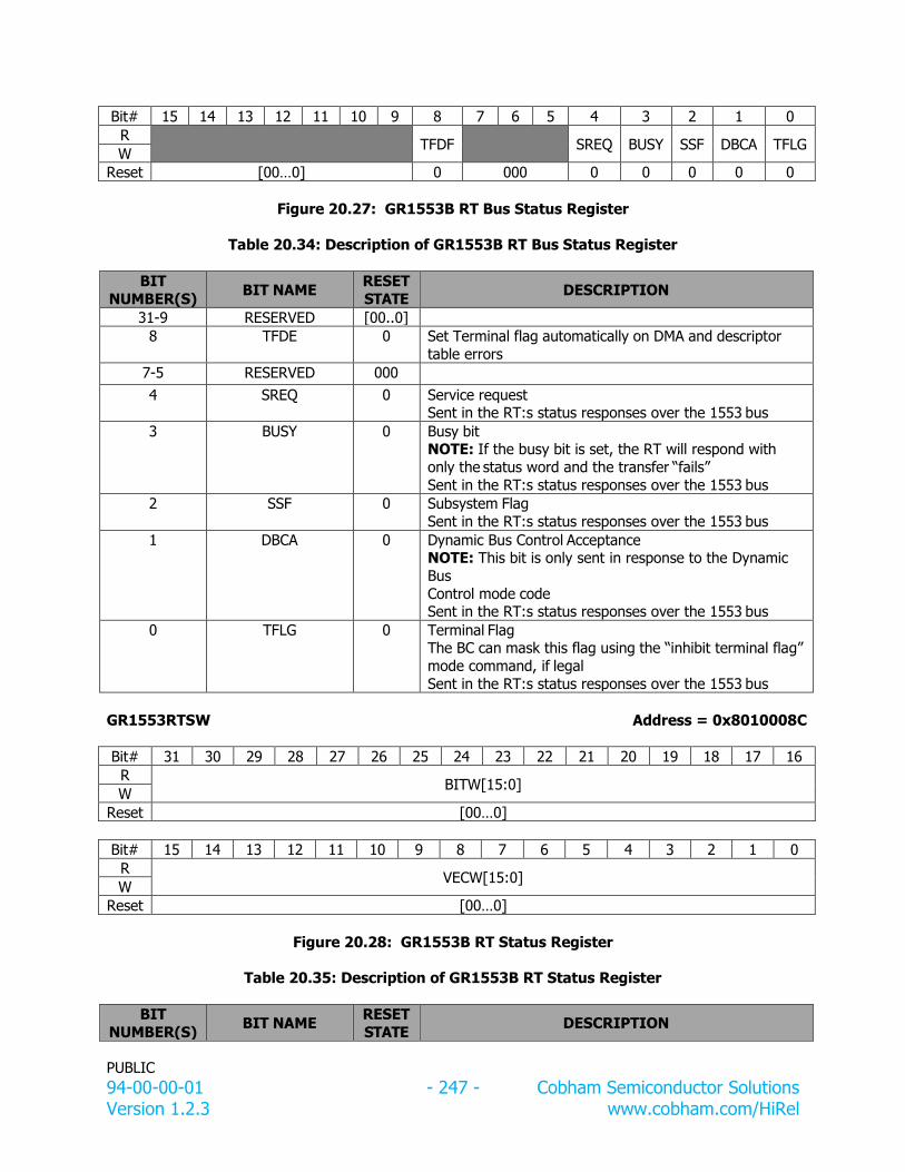
PUBLIC
94-00-00-01 - 247 - Cobham Semiconductor Solutions Version 1.2.3 www.cobham.com/HiRel
Bit# 15 14 13 12 11 10 9 8 7 6 5 4 3 2 1 0
R TFDF SREQ BUSY SSF DBCA TFLG
W
Reset [00…0] 0 000 0 0 0 0 0
Figure 20.27: GR1553B RT Bus Status Register
Table 20.34: Description of GR1553B RT Bus Status Register
BIT
NUMBER(S) BIT NAME
RESET
STATE DESCRIPTION
31-9 RESERVED [00..0]
8 TFDE 0 Set Terminal flag automatically on DMA and descriptor
table errors
7-5 RESERVED 000 4 SREQ 0 Service request
Sent in the RT:s status responses over the 1553 bus
3 BUSY 0 Busy bit NOTE: If the busy bit is set, the RT will respond with
only the status word and the transfer “fails”
Sent in the RT:s status responses over the 1553 bus
2 SSF 0 Subsystem Flag
Sent in the RT:s status responses over the 1553 bus
1 DBCA 0 Dynamic Bus Control Acceptance NOTE: This bit is only sent in response to the Dynamic
Bus
Control mode code Sent in the RT:s status responses over the 1553 bus
0 TFLG 0 Terminal Flag The BC can mask this flag using the “inhibit terminal flag”
mode command, if legal
Sent in the RT:s status responses over the 1553 bus
GR1553RTSW Address = 0x8010008C
Bit# 31 30 29 28 27 26 25 24 23 22 21 20 19 18 17 16
R BITW[15:0]
W
Reset [00…0]
Bit# 15 14 13 12 11 10 9 8 7 6 5 4 3 2 1 0
R VECW[15:0]
W
Reset [00…0]
Figure 20.28: GR1553B RT Status Register
Table 20.35: Description of GR1553B RT Status Register
BIT
NUMBER(S) BIT NAME
RESET
STATE DESCRIPTION

PUBLIC
94-00-00-01 - 248 - Cobham Semiconductor Solutions Version 1.2.3 www.cobham.com/HiRel
BIT
NUMBER(S) BIT NAME
RESET
STATE DESCRIPTION
31-16 BITW [00...0] BIT Word Transmitted in response to the “Transmit BIT Word”
mode command, if legal.
15-0 VECW [00...0] Vector word
Transmitted in response to the “Transmit vector word”
mode command, if legal.
GR1553RTSY Address = 0x80100090
Bit# 31 30 29 28 27 26 25 24 23 22 21 20 19 18 17 16
R SYTM[15:0]
W
Reset [00…0]
Bit# 15 14 13 12 11 10 9 8 7 6 5 4 3 2 1 0
R SYD[15:0]
W
Reset [00…0]
Figure 20.29: GR1553B RT Sync Register
Table 20.36: Description of GR1553B RT Sync Register
BIT
NUMBER(S) BIT NAME
RESET
STATE DESCRIPTION
31-16 SYTM [00...0] The value of the RT timer at the last sync or sync with
data word mode command, if legal.
15-0 SYD [00...0] The data received with the last synchronize with data word mode command, if legal.
GR1553RTST Address = 0x80100094
Bit# 31 30 29 28 27 26 25 24 23 22 21 20 19 18 17 16
R SATB[31:16]
W
Reset [00..0]
Bit# 15 14 13 12 11 10 9 8 7 6 5 4 3 2 1 0
R SATB[15:9]
W
Reset [00…0] [00…0]
Figure 20.30: GR1553B RT Sub Address Table Base Address Register
Table 20.37: Description of GR1553B RT Sub Address Table Base Address Register
BIT
NUMBER(S) BIT NAME
RESET
STATE DESCRIPTION
31-9 SATB [00...0] Base address, bits 31-9 for sub address table

PUBLIC
94-00-00-01 - 249 - Cobham Semiconductor Solutions Version 1.2.3 www.cobham.com/HiRel
BIT
NUMBER(S) BIT NAME
RESET
STATE DESCRIPTION
8-0 RESERVED [00...0]
GR1553RTEL Address = 0x801000B4
Bit# 31 30 29 28 27 26 25 24 23 22 21 20 19 18 17 16
R ELIP[31:16]
W
Reset [00…0]
Bit# 15 14 13 12 11 10 9 8 7 6 5 4 3 2 1 0
R ELIP[15:0]
W
Reset [00…0]
Figure 20.31: GR1553B RT Event Log Interrupt Position Register
Table 20.38: Description of GR1553B RT Event Log Interrupt Position Register
BIT
NUMBER(S) BIT NAME
RESET
STATE DESCRIPTION
31-0 ELIP [00...0] Address to event log entry corresponding to interrupt, 32-bit aligned
The register is set for the first interrupt and not set again until the interrupt has been acknowledged.
GR1553RTMC Address = 0x80100098
Bit# 31 30 29 28 27 26 25 24 23 22 21 20 19 18 17 16
R RRTB[1:0] RRT[1:0] ITFB[1:0] ITF[1:0] ISTB[1:0] IST[1:0] DBC[1:0]
W
Reset 00 00 00 00 00 00 00 00
Bit# 15 14 13 12 11 10 9 8 7 6 5 4 3 2 1 0
R TBW[1:0] TVW[1:0] TSB[1:0] TS[1:0] SDB[1:0] SD[1:0] SB[1:0] S[1:0]
W
Reset 00 00 00 00 00 00 00 00
Figure 20.32: GR1553B RT Mode Code Control Register
Table 20.39: Description of GR1553B RT Mode Code Control Register
BIT NUMBER(S)
BIT NAME RESET STATE
DESCRIPTION
31-30 RESERVED 00 29-28 RRTB 00 Reset remote terminal broadcast
27-26 RRT 00 Reset remote terminal
25-24 ITFB 00 Inhibit & override inhibit terminal flag bit broadcast
23-22 ITF 00 Inhibit & override inhibit terminal flag
21-20 ISTB 00 Initiate self-test broadcast

PUBLIC
94-00-00-01 - 250 - Cobham Semiconductor Solutions Version 1.2.3 www.cobham.com/HiRel
BIT
NUMBER(S) BIT NAME
RESET
STATE DESCRIPTION
19-18 IST 00 Initiate self-test
17-16 DBC 00 Dynamic bus control
15-14 TBW 00 Transmit BIT word
13-12 TVW 00 Transmit vector word
11-10 TSB 01 Transmitter shutdown & override transmitter shutdown broad- cast
9-8 TS 01 Transmitter shutdown & override transmitter shutdown
7-6 SDB 01 Synchronize with data word broadcast
5-4 SD 01 Synchronize with data word
3-2 SB 01 Synchronize broadcast (SB)
1-0 S 01 Synchronize (S)
NOTE: For each mode code: “00” - Illegal, “01” - Legal, “10” - Legal, log enabled, “11” - Legal,
log and interrupt
GR1553RTTT Address = 0x801000A4
Bit# 31 30 29 28 27 26 25 24 23 22 21 20 19 18 17 16
R TRES[15:0]
W
Reset [00…0]
Bit# 15 14 13 12 11 10 9 8 7 6 5 4 3 2 1 0
R TVAL[15:0]
W
Reset [00…0]
Figure 20.33: GR1553B RT Time Tag Control Register
Table 20.40: Description of GR1553B RT Time Tag Control Register
BIT
NUMBER(S) BIT NAME
RESET
STATE DESCRIPTION
31-16 TRES [00...0] Time tag resolution Time unit of RT:s time tag counter in microseconds,
minus 1
15-0 TVAL [00...0] Time tag value Current value of running time tag counter
GR1553RTLS Address = 0x801000AC
Bit# 31 30 29 28 27 26 25 24 23 22 21 20 19 18 17 16
R ELSNM[17:13]
W
Reset [00…0] [11…1]
Bit# 15 14 13 12 11 10 9 8 7 6 5 4 3 2 1 0
R ELSNM[13:0]
W
Reset [11…1] 00

PUBLIC
94-00-00-01 - 251 - Cobham Semiconductor Solutions Version 1.2.3 www.cobham.com/HiRel
Figure 20.34: GR1553B RT Event Log Size Mask Register
Table 20.41: Description of GR1553B RT Event Log Size Mask Register
BIT NUMBER(S)
BIT NAME RESET STATE
DESCRIPTION
31-21 RESERVED [00…0] Always reads “0”
20-2 ELSNM [11..1] Mask determining size and alignment of the RT event log ring buffer. All bits “above” the size should be set to ‘1’, all
bits below should be set to ‘0’.
1-0 RESERVED 00 Always reads ‘0’
GR1553RTELP Address = 0x801000B0
Bit# 31 30 29 28 27 26 25 24 23 22 21 20 19 18 17 16
R ELWP[31:16]
W
Reset [00…0]
Bit# 15 14 13 12 11 10 9 8 7 6 5 4 3 2 1 0
R ELWP[15:0]
W
Reset [00…0]
Figure 20.35: GR1553B RT Event Log Position Register
Table 20.42: Description of GR1553B RT Event Log Position Register
BIT
NUMBER(S) BIT NAME
RESET
STATE DESCRIPTION
31-0 ELWP [00...0] Address to first un used/oldest entry of event log buffer, 32-bit aligned.
GR1553BMS Address = 0x801000C0
Bit# 31 30 29 28 27 26 25 24 23 22 21 20 19 18 17 16
R BMSUP KEYEN
W
Reset 1 0 [00…0]
Bit# 15 14 13 12 11 10 9 8 7 6 5 4 3 2 1 0
R
W
Reset [00…0]
Figure 20.36: GR1553B BM Status Register
Table 20.43: Description of GR1553B BM Status Register
BIT NUMBER(S)
BIT NAME RESET STATE
DESCRIPTION

PUBLIC
94-00-00-01 - 252 - Cobham Semiconductor Solutions Version 1.2.3 www.cobham.com/HiRel
BIT
NUMBER(S) BIT NAME
RESET
STATE DESCRIPTION
31 BMSUP 1 BM Supported Reads ‘1’ if BM support is in the core.
30 KEYEN 0 Key Enabled Reads ‘1’ if the BM validates the BMKEY field when the
control register is written.
29-0 RESERVED [00...0] GR1553BMC Address = 0x801000C4
Bit# 31 30 29 28 27 26 25 24 23 22 21 20 19 18 17 16
R
W
Reset [00…0]
Bit# 15 14 13 12 11 10 9 8 7 6 5 4 3 2 1 0
R WRSTP EXST IMCL UDWL MANL BMEN
W
Reset [00…0] 0 0 0 0 0 0
Figure 20.37: GR1553B BM Control Register
Table 20.44: Description of GR1553B BM Control Register
BIT
NUMBER(S) BIT NAME
RESET
STATE DESCRIPTION
31-6 RESERVED [00...0] 5 WRSTP 0 Wrap stop
If set to ‘1’, BMEN will be set to ‘0’ and stop the BM when
the BM log position wraps around from buffer end to buffer start
4 EXST 0 External sync start
If set to ‘1’, BMEN will be set to ‘1’ and the BM is started when an external BC sync pulse is received
3 IMCL 0 Invalid mode code log
Set to ‘1’ to log invalid or RESERVED mode codes.
2 UDWL 0 Unexpected data word logging
Set to ‘1’ to log data words not seeming to be part of any
command
1 MANL 0 Manchester/parity error logging Set to ‘1’ to log bit
decoding errors
0 BMEN 0 BM Enable Must be set to ‘1’ to enable any BM logging

PUBLIC
94-00-00-01 - 253 - Cobham Semiconductor Solutions Version 1.2.3 www.cobham.com/HiRel
GR1553BMAF Address = 0x801000C8
Bit# 31 30 29 28 27 26 25 24 23 22 21 20 19 18 17 16
R LBTE AFM[30:16]
W
Reset 0 [11…1]
Bit# 15 14 13 12 11 10 9 8 7 6 5 4 3 2 1 0
R AFM[15:0]
W
Reset [11…1]
Figure 20.38: GR1553B BM RT Address Filter Register
Table 20.45: Description of GR1553B BM RT Address Filter Register
BIT
NUMBER(S) BIT NAME
RESET
STATE DESCRIPTION
31 LBTE 1 Enables logging of broadcast transfers
30-0 AFM [11…1] Each bit position set to ‘1’ enables logging of transfers
with the corresponding RT address.
GR1553BMSF Address = 0x801000CC
Bit# 31 30 29 28 27 26 25 24 23 22 21 20 19 18 17 16
R LMC31 SFM[29:15]
W
Reset 1 [11…1]
Bit# 15 14 13 12 11 10 9 8 7 6 5 4 3 2 1 0
R SFM[14:0] LMCE0
W
Reset [11…1] 1
Figure 20.39: GR1553B BM RT Sub Address Filter Register
Table 20.46: Description of GR1553B BM RT Sub Address Filter Register
BIT
NUMBER(S) BIT NAME
RESET
STATE DESCRIPTION
31 LMCE31 1 Enables logging of mode commands on sub-address 31
30-1 SFM [11…1] Each bit position set to ‘1’ enables logging of transfers with the corresponding RT sub-address.
0 LMCE0 1 Enables logging of mode commands on sub-address 0
GR1553BMMC Address = 0x801000D0
Bit# 31 30 29 28 27 26 25 24 23 22 21 20 19 18 17 16
R STSB STS TLC
W
Reset [11…1] 1 1 1

PUBLIC
94-00-00-01 - 254 - Cobham Semiconductor Solutions Version 1.2.3 www.cobham.com/HiRel
Bit# 15 14 13 12 11 10 9 8 7 6 5 4 3 2 1 0
R TSW RRTB RRT ITFB ITF ISTB IST DBC TBW TVW TSB TS SDB SD SB S
W
Reset 1 1 1 1 1 1 1 1 1 1 1 1 1 1 1 1
Figure 20.40: GR1553B BM RT Mode Code Filter Register
Table 20.47: Description of GR1553B BM RT Mode Code Filter Register
BIT NUMBER(S)
BIT NAME RESET STATE
DESCRIPTION
31-19 RESERVED [11...1] 18 STSB 1 Selected transmitter shutdown broadcast & override
selected transmitter shutdown broadcast
17 STS 1 Selected transmitter shutdown & override selected
transmitter shutdown
16 TLC 1 Transmit last command
15 TSW 1 Transmit status word
14 RRTB 1 Reset remote terminal broadcast
13 RRT 1 Reset remote terminal
12 ITFB 1 Inhibit & override inhibit terminal flag bit broadcast
11 ITF 1 Inhibit & override inhibit terminal flag
10 ISTB 1 Initiate self-test broadcast
9 IST 1 Initiate self-test
8 DBC 1 Dynamic bus control
7 TBW 1 Transmit BIT word
6 TVW 1 Transmit vector word
5 TSB 1 Transmitter shutdown & override transmitter shutdown
broadcast
4 TS 1 Transmitter shutdown & override transmitter shutdown
3 SDB 1 Synchronize with data word broadcast
2 SD 1 Synchronize with data word
1 SB 1 Synchronize broadcast
0 S 1 Synchronize
GR1553BMLB Address = 0x801000D4
Bit# 31 30 29 28 27 26 25 24 23 22 21 20 19 18 17 16
R BLBS[31:16]
W
Reset [00…0]
Bit# 15 14 13 12 11 10 9 8 7 6 5 4 3 2 1 0
R BLBS[15:0]
W
Reset [00…0]
Figure 20.41: GR1553B BM Log Buffer Start

PUBLIC
94-00-00-01 - 255 - Cobham Semiconductor Solutions Version 1.2.3 www.cobham.com/HiRel
Table 20.48: Description of GR1553B BM Log Buffer Start
BIT
NUMBER(S) BIT NAME
RESET
STATE DESCRIPTION
31-0 BLBS [00...0] Pointer to the lowest address of the BM log buffer (8-byte aligned)
Due to alignment, bits 2:0 are always 0.
GR1553BMLE Address = 0x801000D8
Bit# 31 30 29 28 27 26 25 24 23 22 21 20 19 18 17 16
R BLBE[31:16]
W
Reset [00…0]
Bit# 15 14 13 12 11 10 9 8 7 6 5 4 3 2 1 0
R BLBE[15:0]
W
Reset 0x0007
Figure 20.42: GR1553B BM Log Buffer End
Table 20.49: Description of GR1553B BM Log Buffer End
BIT
NUMBER(S) BIT NAME
RESET
STATE DESCRIPTION
31-0 BLBE 0x00000007
Pointer to the highest address of the BM log buffer Only bits 21:3 are settable, i.e. the buffer can not cross a
4 MB boundary Bits 31:22 read the same as the buffer start address. Due to alignment, bits 2:0 are always equal
to 1.
GR1553BMTT Address = 0x801000E0
Bit# 31 30 29 28 27 26 25 24 23 22 21 20 19 18 17 16
R TTR[7:0] TTV[23:16]
W
Reset [00…0] [00…0]
Bit# 15 14 13 12 11 10 9 8 7 6 5 4 3 2 1 0
R TTV[15:0]
W
Reset [00…0]
Figure 20.43: GR1553B BM Time Tag Control Register
Table 20.50: Description of GR1553B BM Time Tag Control Register
BIT NUMBER(S)
BIT NAME RESET STATE
DESCRIPTION
31-24 TTR [00...0] Time tag resolution
Time unit of BM:s time tag counter in micro- seconds,

PUBLIC
94-00-00-01 - 256 - Cobham Semiconductor Solutions Version 1.2.3 www.cobham.com/HiRel
BIT
NUMBER(S) BIT NAME
RESET
STATE DESCRIPTION
minus 1
23-0 TTV [00...0] Time tag value
Current value of running time tag counter
GR1553BMLBP Address = 0x801000DC
Bit# 31 30 29 28 27 26 25 24 23 22 21 20 19 18 17 16
R BLP[31:16]
W
Reset [00…0]
Bit# 15 14 13 12 11 10 9 8 7 6 5 4 3 2 1 0
R BLP[15:0]
W
Reset [00…0]
Figure 20.44: GR1553B BM Log Buffer Position
Table 20.51: Description of GR1553B BM Log Buffer Position
BIT
NUMBER(S) BIT NAME
RESET
STATE DESCRIPTION
31-0 BLP [00...0] Pointer to the next position that will be written to in the BM log buffer
Only bits 21:3 are settable, i.e. the buffer cannot cross a 4 MB boundary Bits 31:22 read the same as the buffer
start address. Due to alignment, bits 2:0 are always
equal to 0.

PUBLIC
94-00-00-01 - 257 - Cobham Semiconductor Solutions Version 1.2.3 www.cobham.com/HiRel
Appendix A: Register Format MCFG2 Address = 0x8000_0004
Bit# 31 30 29 28 27 26 25 24 23 22 21 20 19 18 17 16 R
DR DP DF[2:0] DC DZ[2:0] DS[1:0] DD[1:0] BW PB
W Reset 0 1 111 1 000 10 00 0 0 0 Bit# 15 14 13 12 11 10 9 8 7 6 5 4 3 2 1 0
R DE SI SZ[3:0] SB RM SD[1:0] SW[1:0] SR[1:0]
W Reset 0 0 0 -- 0 0 - -- 00 00
Legend: Bit# Bit Number
R Read Operation W Write Operation Don’t Care Reserved -- Reset State, Not Initialized 0 Reset State is 0 1 Reset State is 1

PUBLIC
94-00-00-01 - 258 - Cobham Semiconductor Solutions Version 1.2.3 www.cobham.com/HiRel
Appendix B: Errata
UT700 MIL-STD-1553 NOISE REJECTION LIMITATIONS
Table 21.1: Description of GR1553B BM Log Buffer Position
Product Name: Manufacturer
Part Number SMD # Device Type
Internal PIC
Number
UT700 LEON 3FT
Microprocessor
UT700 5962-13238 All WQ03
Overview/Problem Statement MIL-STD-1553 paragraph 5.3 requires a terminal to pass a noise rejection test to ensure correct interoperability while exposed to a noisy environment. The noise rejection test requires
injecting a band limited, 1.0K to 4MHz, White Gaussian noise at 140mVrms (transformer coupled) or 200mVrms (direct coupled) on the bus and transmitting a minimum of 40,000,000
data words without any message errors. This erratum explains why meeting the noise rejection
test is a challenge for the GR1553 core contained in the UT700.
Technical Background The GR1553 is a MIL-STD-1553 compliant protocol controller for the UT700. The GR1553 has the ability to operate as a Remote Terminal, Bus Controller, and Bus Monitor. Certification of a
MIL-STD-1553 device typically involves testing the Remote Terminal operations. The GR1553
protocol controller is configured to operate as a Re-mote Terminal during the certification testing. The noise rejection test results are a function of the protocol controller as well as the
transceiver and transformer. It is typical of most transceivers to pass a narrow pulse as a result of noise on the bus. Protocol controllers designed to filter the narrow pulses are unaffected.
Since each protocol controller is designed to evaluate the width and proximity of random pulses differently, sensitivity to noise induced pulses will differ between manufactures.
Specific Description of the Problem The MIL-STD-1553 interface used for the UT700 has a potential to fail the noise rejection test requirements specified in MIL-STD-1553 due to two built in features of the GR1553 interface.
The GR1553 has the ability to monitor for invalid sync or parity bits. An invalid sync bit or erroneous glitch occurring within 3μs of a valid message will cause the message to be rejected.
An invalid parity bit will also cause the message to be rejected. Rejecting a message with invalid
symbols is desirable with additional checks to ensure subsequent symbols are not valid. However, the decoder circuit used for the GR1553 interface monitors for pulses greater than
150ns wide and potentially will evaluate the pulse as erroneous or invalid and prevent processing of messages received within 3μs of this pulse. The 3μs window permits time for
controller to reset to an operational state. Also, there are times when the decoder may
interpret the last received parity bit as too wide or too narrow, which would inhibit a response.
Implications Impact on the system/user when encountered:
Remote Terminal validation testing of the UT700 determined that the product passes
the MIL-STD-1553 noise induced word error rate of 1E-7 at noise amplitude of
100mVrms. At noise levels >100mVrms, the associate error rate increased in
accordance with the plot shown in Figure B1.
MIL-STD-1553 testing has a correlation between the message rate and the word rate,
since each transfer consists of a command word and 32 data words. Because the
UT700 error rate is strongly correlated to the idle time just before the command

PUBLIC
94-00-00-01 - 259 - Cobham Semiconductor Solutions Version 1.2.3 www.cobham.com/HiRel
word's sync pulse and right after the final data word's parity bit, the error rate is a
function of the message rate. Assuming a maximum word error rate of 1E-7 that requires a minimum of 303.03 k messages, the maximum message error rate would
be 3.3E-6. Therefore, the retry rate is expected to increase proportionally to the noise level as see in the Figure B1:
Figure B1: UT700 MIL-STD-1553 Message Error Rate vs Noise Amplitude
Workarounds Best practice for PCB layout of transceiver and transformers Designing the PCB with the least amount of skew between receiver input lines on the bus side will help minimize susceptibility to the noise, particularly at zero crossing. Part of the noise
protection in a terminal relies on the filtering capabilities of the transformers; using high quality
transformers will lower the susceptibility to system noise. Additionally, ensuring there are no signal, ground, or power plains beneath the transformers optimizes the transformer filtering
capability. Provide an appropriate budget for noise induced retries Planning for a reduction in performance by allowing system retries for any message where the RT did not provide a response ensures the system meets the mission requirements.
Reduce the noise exposure to the system Enhancing the power filtering, cable shielding, and environmental shielding can reduce the likelihood that noise will affect the system.
Summary/Conclusion and Possible Corrective Action The protocol controller used in the UT700 may prevent passing the noise rejection test as
prescribed by MIL-STD-1553. However, typical space vehicles don’t experience the level of noise specified in MIL-STD-1553, paragraph 5.3. The expected performance reduction in data rate
can be compensated by proper planning of bus traffic and system bandwidth. Additionally, enhanced shielding and best practices applied to the PCB and operating environment will
reduce the susceptibility a system to noise.

PUBLIC
94-00-00-01 - 260 - Cobham Semiconductor Solutions Version 1.2.3 www.cobham.com/HiRel
The following United States (U.S.) Department of Commerce statement shall be applicable
if these commodities, technology, or software are exported from the U.S.: These
commodities, technology, or software were exported from the United States in accordance
with the Export Administration Regulations. Diversion contrary to U.S. law is prohibited.
Aeroflex Colorado Springs, dba Cobham Semiconductor Solutions
4350 Centennial Blvd
Colorado Springs, CO 80907
T: 800 645 8862
Aeroflex Colorado Springs Inc., dba Cobham Semiconductor Solutions, reserves the right to make changes to any products and services described
herein at any time without notice. Consult Aeroflex or an authorized sales representative to verify that the information in this data sheet is current
before using this product. Aeroflex does not assume any responsibility or liability arising out of the application or use of any product or service
described herein, except as expressly agreed to in writing by Aeroflex; nor does the purchase, lease, or use of a product or service from Aeroflex
convey a license under any patent rights, copyrights, trademark rights, or any other of the intellectual rights of Aeroflex or of third parties.

PUBLIC
94-00-00-01 - 261 - Cobham Semiconductor Solutions Version 1.2.3 www.cobham.com/HiRel
REVISION HISTORY
REV Revision Date Description of Change Page(s) Author
1.0.0 11/14 Initial Release Simms
1.1.0 4/15 Added Appendix A: Errata to manual 256-257 Simms
1.1.1 3/16 Edited 2.3 changed 7 to 8. Changed text in
2.4.1.
Edited Table 2.5 interrupt_level_3. Edited
Table 3.4 bit number 17-14. Changed text in 5.2.2.
Deleted duplicate Figure 9.19
Edited Table 12.3 changed 0 to Reset by
GPIO[7.4] Edited 12.8 to 200MHz.
Edited Table 14.9 bit number 7.
19, 55,
163
Stratton
1.1.2 8/16 Changes Register format. Changed text
errors in multiple places. Changed
terminologies in multiple places. Changed Figure 1.1, Figure 16.2 and Figure 19.1.
Delete duplicate chapter 14.
11 to 259 Sim,
Aguas,
Farris
1.1.3 9/16 Section 7.2 changed IP bit clear to ‘1’
Control Register for Timer 1 to 3 reset = 0
Control Register for Timer 4 rest value =
0x09, watchdog is enabled
Edited MFCG3 RSE bit
12 to 209 Sim
1.1.4 10-24-2016 Table 1.7, 18.2, 6.4 19,176,79 Sim
1.1.5 01-25-2017 5.3.7, Note, Register addresses,2.4,website link
78,177,94-97,32,212
Sim
1.1.6 02-27-2017 1.1,Table 1.1, 1.3,2.2.5, 12,13,14,25 Sim
1.1.7 03-22-2017 19.2.3,7.2 243,88 Sim
1.1.8 10-11-2017 Table 2.12 data cache snoop enable = 1,
Figure 19.2, Table 1.5 remove duplicate
entry, Table 12.15, 12.3.3 Add Note:, Table 1.3
38, 128,
213,19,154,15,17
Sim
1.1.9 12/20/2017 Add 2.4.X 31 to 34, MTS
1.2.0 03/28/2018 Add NODIV, FSQRTS and FSQRTD 33 MTS
1.2.1 06/12/2018 UART, MMUCR,MMUCPR, MMUFAR 88,45,46,48 MTS
1.2.2 06/24/2018 New Format (Remove WORD hidden codes) All MTS
1.2.3 09/12/2018 Add EDCL IP and MAC registers 187,188 MTS