Embed Size (px)
Citation preview

The most important thing we build is trust
Standard Products
UT699 LEON 3FT/SPARCTM V8 MicroProcessorFunctional ManualFebruary 2015www.aeroflex.com/LEON
0
Table of Contents
1.0 INTRODUCTION 81.1 Scope 81.2 Architecture 91.3 Memory map 111.4 Interrupts 121.5 Signals 131.6 Clocking 16 1.6.1 Clock inputs 16 1.6.2 Clock gating 16
1.7 Reset Operations 16
2.0 LEON 3FT SPARC V8 32-bit MICROPROCESSOR 172.1 Overview 17
2.1.1 Integer unit 172.1.2 Cache sub-system 172.1.3 Floating-point unit 172.1.4 On-chip debug support 182.1.5 Interrupts 182.1.6 AMBA interface 182.1.7 Power-down mode 18
2.2 LEON 3FT integer unit 182.2.1 Overview 182.2.2 Instruction pipeline 202.2.3 SPARC implementor’s ID 202.2.4 Divide instructions 202.2.5 Multiply instructions 212.2.6 Hardware breakpoints 21
2.2.7 Instruction trace buffer 22 2.2.8 Processor configuration register 22 2.2.9 Exceptions 24 2.2.10 Single vector trapping (SVT) 25 2.2.11 Address space identifiers (ASI) 25 2.2.12 Power-down 25
2.2.13 Processor reset operation 262.2.14 Integer unit SEU protection 262.2.15 Data scrubbing 27
2.3 Floating-point unit 272.4 Cache sub-systems 28
2.4.1 Overview 282.4.2 Instruction cache 282.4.3 Data code 282.4.4 Write buffer 282.4.5 Instruction and data cache tags 292.4.6 Cache flushing 30
2
2.4.7 Diagnostic cache access 2.4.7.1 Diagnostic reads of instruction and data cache 30
2.4.7.2 Diagnostic writes to instruction and data cache 302.4.8 Cache control register 312.4.9 Error protection 332.4.10 Cache configuration registers 332.4.11 Software consideration 35
2.5 Memory management unit 352.5.1 MMU ASI usage 352.5.2 Cache operation 352.5.3 MMU registers 352.5.4 Translation Look-Aside Buffer (TLB) 35
2.6 RAM usage 362.6.1 Integer unit register file 362.6.2 Floating Point Unit (FPU) register file 362.6.3 Cache memories 36
2.6.3.1 Instruction cache tags 36 2.6.3.2 Data cache tags 37 2.6.3.3 Instruction and data cache data memory 37
3.0 MEMORY CONTROLLER with EDAC 383.1 Overview 383.2 PROM access 393.3 Memory mapped I/O 393.4 SRAM access 393.5 8-bit and 16-bit PROM and SRAM access 393.6 8-bit and 16-bit I/O access 413.7 Burst cycles 413.8 SDRAM access 41
3.8.1 General 413.8.2 Address mapping 423.8.3 Initialization 423.8.4 Configurable SDRAM timing parameters 42
3.9 Refresh 423.9.1 SDRAM commands 423.9.2 Read cycles 423.9.3 Write cycles 423.9.4 Address bus 433.9.5 Data bus 433.9.6 Clocking 433.9.7 Initialization 43
3.10 Memory EDAC 433.11 Using BRDY 443.12 Access errors 443.13 Attaching an external DRAM controller 443.14 Registers 44
3.14.1 Memory configuration register 1 (MCFG1) 45
3
3.14.2 Memory configuration register 2 (MCFG2) 46 3.14.3 Memory configuration register 3 (MCFG3) 48
3.15 Vendor and device identifiers 493.16 PROM, SRAM, and memory mapped I/O timing diagrams 493.17 SDRAM timing diagrams 62
4.0 AHB STATUS REGISTERS 644.1 Overview 644.2 Operation 644.3 Registers 64
5.0 INTERRUPT CONTROLLER 655.1 Overview 655.2 Operation 65
5.2.1 Interrupt prioritization 65 5.2.2 Interrupt allocation 66
5.3 Registers 665.3.1 Interrupt level register 675.3.2 Interrupt pending register 675.3.3 Interrupt force register 675.3.4 Interrupt clear register 685.3.5 Interrupt mask register 68
6.0 UART with APB INTERFACE 696.1 Overview 696.2 Operation 69
6.2.1 Transmitter operation 696.2.2 Receiver operation 70
6.3 Baud-rate generation 706.3.1 Loop back mode 706.3.2 Interrupt generation 71
6.4 UART registers 716.4.1 UART data register 716.4.2 UART status register 716.4.3 UART control register 726.4.4 UART scaler register 73
7.0 TIMER UNIT 747.1 Overview 747.2 Operation 747.3 Registers 75
8.0 GENERAL PURPOSE I/O PORT 798.1 Overview 798.2 Operation 798.3 Registers 79
4
8.3.1 GPIO port data value register 80 8.3.2 GPIO port data output register 80 8.3.3 GPIO port data direction register 80 8.3.4 GPIO interrupt mask register 81 8.3.5 GPIO interrupt polarity register 81 8.3.6 GPIO interrupt edge register 82
9.0 PCI TARGET / MASTER UNIT 839.1 Overview 839.2 Operation 83
9.2.1 PCI target unit 839.2.2 PCI master unit 849.2.3 Burst transactions 849.2.4 Byte timing 84
9.3 PCI target interface 849.4 PCI target configuration space header register 859.5 PCI target map registers 90
9.5.1 PAGE0 register 90 9.5.2 PAGE1 register 91
9.6 PCI master interface 91 9.6.1 PCI configuration cycles 92 9.6.2 I/O cycles 92 9.6.3 PCI memory cycles 92
9.7 PCI host operation 949.8 Interrupt Support 949.9 Registers 949.10 Vendor and device identifiers 96
10.0 DMA CONTROLLER for the GRPCI INTERFACE 9710.1 Introduction 9710.2 Operation 9710.3 Registers 9810.4 Vendor and device identifiers 99
11.0 SpaceWire INTERFACE 10011.1 Overview 10011.2 Operations 101
11.2.1 Overview 10111.2.2 Protocol support 101
11.3 Link interface 10211.3.1 Link interface FSM 10211.3.2 Transmitter 10211.3.3 Receiver 10311.3.4 Time interface 10311.3.5 Basic functionality 104
11.4 Receiver DMA engine 104
5
11.4.1 Basic functionality 10411.4.2 Setting up the GRSPW for reception 10411.4.3 Setting up the descriptor table address 10511.4.4 Enabling descriptors 10511.4.5 Setting up the DMA control register 10711.4.6 The effect to the control bits during reception 10711.4.7 Address recognition and packet handling 10711.4.8 Status bits 10711.4.9 Error handling 10811.4.10 Open packet mode 108
11.5 Transmitter DMA engine 10811.5.1 Basic functionality 10811.5.2 Setting up the GRSPW for transmission 10811.5.3 Enabling descriptors 10811.5.4 Starting transmissions 10911.5.5 The transmission process 11111.5.6 The descriptor table address 11111.5.7 Error handling 111
11.6 RMAP 11111.6.1 Fundamentals of the protocol 11211.6.2 Implementation 11211.6.3 Write commands 11411.6.4 Read commands 11411.6.5 RMW commands 11411.6.6 Control 114
11.7 AMBA interface 11811.7.1 APB slave interface 11811.7.2 AHB master interface 118
11.8 Registers 118
12.0 CAN-2.0 Interface 12812.1 Overview 12812.2 AHB interface 12812.3 BasicCan mode 129
12.3.1 BasicCan register map 12912.3.2 Control register 13012.3.3 Command register 13012.3.4 Status register 13112.3.5 Interrupt register 13112.3.6 Transmit buffer 13212.3.7 Receiver buffer 13212.3.8 Acceptance filter 132
12.4 PeliCAN mode 13312.4.1 PeliCAN register map 13312.4.2 Mode register 13412.4.3 Command register 134
6
12.4.4 Status register 13512.4.5 Interrupt register 13512.4.6 Interrupt enable register 13612.4.7 Arbitration lost capture register 13612.4.8 Error code capture register 13612.4.9 Error warning limit register 13812.4.10 RX error counter register (address 14) 13812.4.11 TX error counter register (address 15) 13812.4.12 Transmit buffer 13812.4.13 Receive buffer 14112.4.14 Acceptance filter 14312.4.15 RX message center 145
12.5 Common registers 14512.5.1 Clock divider register 14512.5.2 Bus timing 0 14612.5.3 Bus timing 1 146
12.6 Design considerations 146
13.0 ETHERNET MEDIA ACCESS CONTROLLER (MCA) 14713.1 Overview 14713.2 Operation 147
13.2.1 System overview 14713.2.2 Protocol support 14813.2.3 Hardware requirements 14813.2.4 Transmitter DMA interface 14813.2.5 Setting up a descriptor 14813.2.6 Starting transmissions 14913.2.7 Descriptor handling after transmission 15013.2.8 Setting up the data for transmission 15013.2.9 Receiver DMA interface 15013.2.10 Setting up descriptors 15013.2.11 Starting reception 15113.2.12 Descriptor handling after reception 15213.2.13 Reception with AHB errors 15213.2.14 MDIO interface 15213.2.15 Media independent interfaces 15213.2.16 Software drivers 152
13.3 Registers 15313.3.1 Vendor and device identifiers 157
14.0 HARDWARE DEBUG SUPPORT 15814.1 Introduction 15814.2 Operation 15814.3 AHB trace buffer 15914.4 Instruction trace buffer 16014.5 DSU memory map 160
7
14.6 DSU registers 16214.6.1 DSU control register 16214.6.2 DSU break and signal-step register 16314.6.3 DSU trap register 16314.6.4 DSU trace buffer time tag counter register 16414.6.5 DSU ASI diagnostic access register 16414.6.6 AHB trace buffer control register 16414.6.7 AHB trace buffer index register 16514.6.8 AHB trace buffer breakpoint registers 16514.6.9 Instruction trace control register 166
15.0 SERIAL DEBUG LINK 16715.1 Overview 16715.2 Operation 167
15.2.1 Transmission protocol 16715.2.2 Baud rate generation 168
15.3 Registers 168
16.0 JTAG DEBUT LINK 17016.1 Overview 17016.2 Operation 17016.3 Registers 17116.4 Vendor and device identifiers 171
17.0 CLKGATE CLOCK GATING UNIT 17217.1 Overview 17217.2 Operation 17217.3 Registers 17317.4 Vendor and device identifiers 173
EDIT HISTORY 175
APPLICATION NOTES 184
8
1.0 Introduction
1.1 Scope
This document describes the UT699 LEON 3FT microprocessor. The UT699 is a pipelined, monolithic, high-performance, fault-tolerant SPARCTM V8 Processor. It has been designed for reliable operation in HiRel environments; the architecture includes functionality to detect and correct (SEU) errors in all on-chip RAM memories.
The UT699 provides a 32-bit/33MHz PCI (Revision 2.1 compatible) master/target interface with DMA and host capabilities, including a 16-bit user I/O interface for off-chip peripherals. An AMBA (Rev. 2.0) bus interface integrates the on-chip LEON 3FT core, SpaceWire, Ethernet, memory controller, PCI, CAN bus, and programmable interrupt peripherals.
The UT699 is SPARC V8 compliant. Therefore, industry standard compilers and kernels for the SPARC V8 can be used for software development. A full software development suite, including a C/C++ cross-compiler system based on the Gnu C Compiler (GCC) and the Newlib embedded C-library is available from Aeroflex Gaisler. The Bare C Compiler (BCC), based upon GCC, includes a small run-time kernel with interrupt support and Pthreads library. The development suite runs on either Windows or Linux operating systems. For multi-threaded applications, a SPARC compliant port of the eCos real-time kernel, RTEMS 4.6.5 and VxWorks 6.x is supported.
The UT699 LEON 3FT microprocessor is based on IP cores from Aeroflex Gaisler AB’s GRLIB Intellectual Property (IP) library and uses a plug-and-play configuration.
9
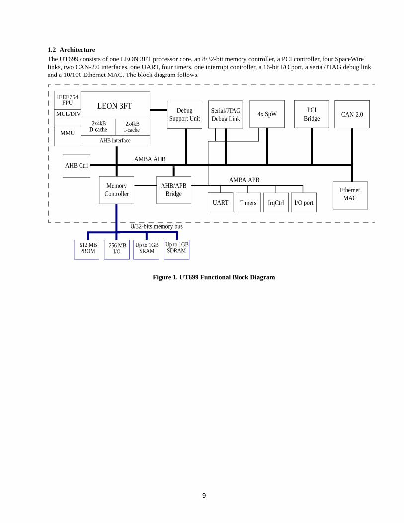
1.2 Architecture
The UT699 consists of one LEON 3FT processor core, an 8/32-bit memory controller, a PCI controller, four SpaceWire links, two CAN-2.0 interfaces, one UART, four timers, one interrupt controller, a 16-bit I/O port, a serial/JTAG debug link and a 10/100 Ethernet MAC. The block diagram follows.
2x4kB
AMBA AHB
Timers IrqCtrl
AMBA APB
8/32-bits memory bus
DebugSupport Unit
AHB interface
LEON 3FT
MemoryController
AHB/APBBridge
I/O portUART
IEEE754FPU
MUL/DIV
MMU
PCICAN-2.0
AHB Ctrl
Serial/JTAGDebug Link
4x SpWBridge
EthernetMAC
D-cache 2x4kB
I-cache
512 MBPROM
256 MBI/O
Up to 1GB SRAM
D-cache
Up to 1GBSDRAM
Figure 1. UT699 Functional Block Diagram
10
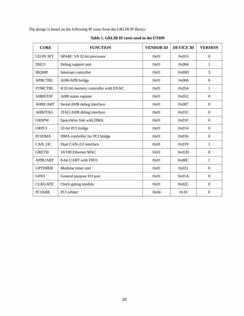
The design is based on the following IP cores from the GRLIB IP library:
Table 1. GRLIB IP cores used in the UT699
CORE FUNCTION VENDOR ID DEVICE ID VERSION
LEON 3FT SPARC V8 32-bit processor 0x01 0x053 0
DSU3 Debug support unit 0x01 0x004 1
IRQMP Interrupt controller 0x01 0x00D 3
APBCTRL AHB/APB bridge 0x01 0x006 0
FTMCTRL 8/32-bit memory controller with EDAC 0x01 0x054 1
AHBSTAT AHB status register 0x01 0x052 0
AHBUART Serial/AHB debug interface 0x01 0x007 0
AHBJTAG JTAG/AHB debug interface 0x01 0x01C 0
GRSPW SpaceWire link with DMA 0x01 0x01F 0
GRPCI 32-bit PCI bridge 0x01 0x014 0
PCIDMA DMA controller for PCI bridge 0x01 0x016 0
CAN_OC Dual CAN-2.0 interface 0x01 0x019 1
GRETH 10/100 Ethernet MAC 0x01 0x01D 0
APBUART 8-bit UART with FIFO 0x01 0x00C 1
GPTIMER Modular timer unit 0x01 0x011 0
GPIO General purpose I/O port 0x01 0x01A 0
CLKGATE Clock gating module 0x01 0x02C 0
PCIARB PCI arbiter 0x04 0x10 0
11
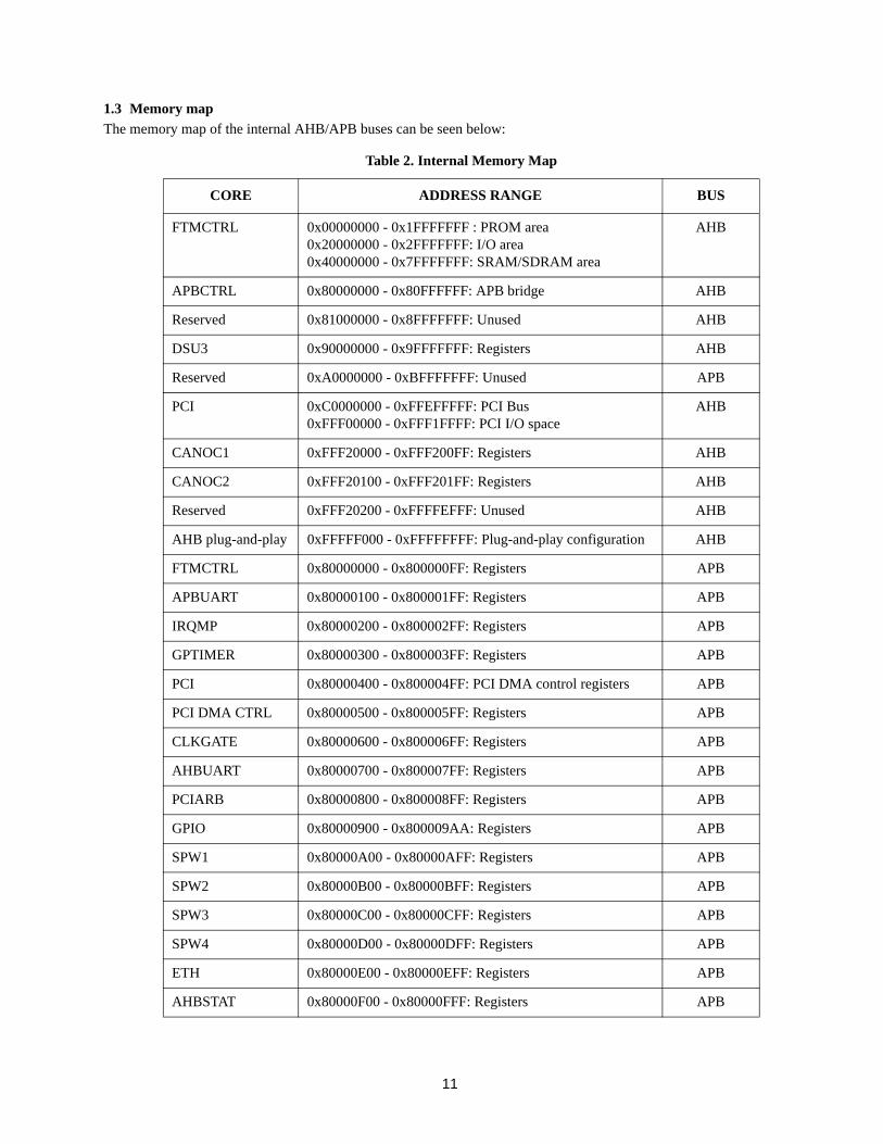
1.3 Memory map
The memory map of the internal AHB/APB buses can be seen below:
Table 2. Internal Memory Map
CORE ADDRESS RANGE BUS
FTMCTRL 0x00000000 - 0x1FFFFFFF : PROM area0x20000000 - 0x2FFFFFFF: I/O area0x40000000 - 0x7FFFFFFF: SRAM/SDRAM area
AHB
APBCTRL 0x80000000 - 0x80FFFFFF: APB bridge AHB
Reserved 0x81000000 - 0x8FFFFFFF: Unused AHB
DSU3 0x90000000 - 0x9FFFFFFF: Registers AHB
Reserved 0xA0000000 - 0xBFFFFFFF: Unused APB
PCI 0xC0000000 - 0xFFEFFFFF: PCI Bus 0xFFF00000 - 0xFFF1FFFF: PCI I/O space
AHB
CANOC1 0xFFF20000 - 0xFFF200FF: Registers AHB
CANOC2 0xFFF20100 - 0xFFF201FF: Registers AHB
Reserved 0xFFF20200 - 0xFFFFEFFF: Unused AHB
AHB plug-and-play 0xFFFFF000 - 0xFFFFFFFF: Plug-and-play configuration AHB
FTMCTRL 0x80000000 - 0x800000FF: Registers APB
APBUART 0x80000100 - 0x800001FF: Registers APB
IRQMP 0x80000200 - 0x800002FF: Registers APB
GPTIMER 0x80000300 - 0x800003FF: Registers APB
PCI 0x80000400 - 0x800004FF: PCI DMA control registers APB
PCI DMA CTRL 0x80000500 - 0x800005FF: Registers APB
CLKGATE 0x80000600 - 0x800006FF: Registers APB
AHBUART 0x80000700 - 0x800007FF: Registers APB
PCIARB 0x80000800 - 0x800008FF: Registers APB
GPIO 0x80000900 - 0x800009AA: Registers APB
SPW1 0x80000A00 - 0x80000AFF: Registers APB
SPW2 0x80000B00 - 0x80000BFF: Registers APB
SPW3 0x80000C00 - 0x80000CFF: Registers APB
SPW4 0x80000D00 - 0x80000DFF: Registers APB
ETH 0x80000E00 - 0x80000EFF: Registers APB
AHBSTAT 0x80000F00 - 0x80000FFF: Registers APB
12
Access to addresses outside the ranges described above will return an AHB error response.
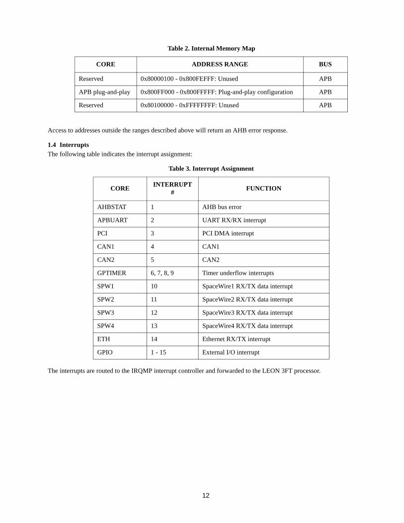
1.4 Interrupts
The following table indicates the interrupt assignment:
The interrupts are routed to the IRQMP interrupt controller and forwarded to the LEON 3FT processor.
Reserved 0x80000100 - 0x800FEFFF: Unused APB
APB plug-and-play 0x800FF000 - 0x800FFFFF: Plug-and-play configuration APB
Reserved 0x80100000 - 0xFFFFFFFF: Unused APB
Table 3. Interrupt Assignment
COREINTERRUPT
#FUNCTION
AHBSTAT 1 AHB bus error
APBUART 2 UART RX/RX interrupt
PCI 3 PCI DMA interrupt
CAN1 4 CAN1
CAN2 5 CAN2
GPTIMER 6, 7, 8, 9 Timer underflow interrupts
SPW1 10 SpaceWire1 RX/TX data interrupt
SPW2 11 SpaceWire2 RX/TX data interrupt
SPW3 12 SpaceWire3 RX/TX data interrupt
SPW4 13 SpaceWire4 RX/TX data interrupt
ETH 14 Ethernet RX/TX interrupt
GPIO 1 - 15 External I/O interrupt
Table 2. Internal Memory Map
CORE ADDRESS RANGE BUS
13
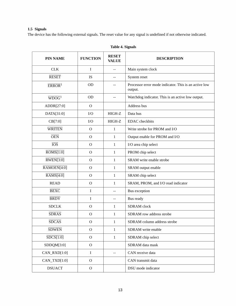
1.5 Signals
The device has the following external signals. The reset value for any signal is undefined if not otherwise indicated.
Table 4. Signals
PIN NAME FUNCTIONRESET VALUE
DESCRIPTION
CLK I -- Main system clock
RESET IS -- System reset
ERROR1 OD -- Processor error mode indicator. This is an active low output.
WDOG1 OD -- Watchdog indicator. This is an active low output.
ADDR[27:0] O Address bus
DATA[31:0] I/O HIGH-Z Data bus
CB[7:0] I/O HIGH-Z EDAC checkbits
WRITEN O 1 Write strobe for PROM and I/O
OEN O 1 Output enable for PROM and I/O
IOS O 1 I/O area chip select
ROMS[1:0] O 1 PROM chip select
RWEN[3:0] O 1 SRAM write enable strobe
RAMOEN[4:0] O 1 SRAM output enable
RAMS[4:0] O 1 SRAM chip select
READ O 1 SRAM, PROM, and I/O read indicator
BEXC I -- Bus exception
BRDY I -- Bus ready
SDCLK O 1 SDRAM clock
SDRAS O 1 SDRAM row address strobe
SDCAS O 1 SDRAM column address strobe
SDWEN O 1 SDRAM write enable
SDCS[1:0] O 1 SDRAM chip select
SDDQM[3:0] O SDRAM data mask
CAN_RXD[1:0] I -- CAN receive data
CAN_TXD[1:0] O CAN transmit data
DSUACT O DSU mode indicator
DSUBRE I -- DSU break
DSUEN I -- DSU enable
DSURX I -- DSU UART receive data
DSUTX O DSU UART transmit data
TRST I -- JTAG reset
TMS I -- JTAG test mode select
TCK I -- JTAG clock
TDI I -- JTAG test data input
TDO O JTAG test data output
EMDC O Ethernet media interface clock
ERX_CLK I -- Ethernet RX clock
EMDIO I/O Ethernet media interface data
ERX_COL I -- Ethernet collision error
ERX_CRS I -- Ethernet carrier sense detect
ERX_DV I -- Ethernet receiver data valid
ERX_ER I -- Ethernet reception error
ERXD[3:0] I -- Ethernet receive data
ETXD[3:0] O Ethernet transmit data
ETX_CLK I -- Ethernet TX clock
ETX_EN O Ethernet transmit enable
ETX_ER O Ethernet transmit error
ETXD[3:1] O Ethernet transmit data
ETX_CLK I -- Ethernet TX clock
ETX_EN O Ethernet transmit enable
ETX_ER O Ethernet transmit error
GPIO[15:0] I/O General Purpose I/O
SPW_CLK I -- SpaceWire clock
SPW_RXS[3:0] I -- SpaceWire receive strobe
SPW_RXD[3:0] I -- SpaceWire receive data
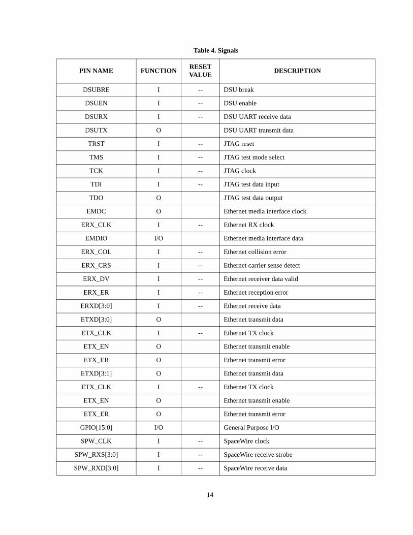
Table 4. Signals
PIN NAME FUNCTIONRESET VALUE
DESCRIPTION
14
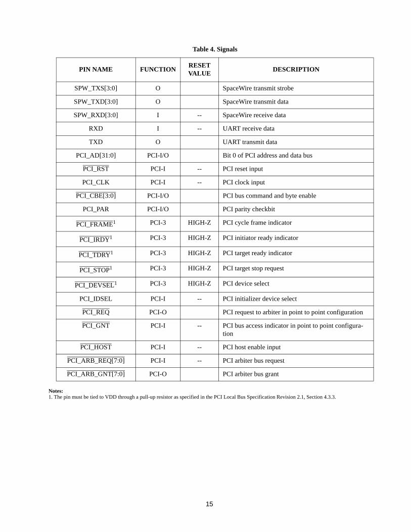
15
Notes:1. The pin must be tied to VDD through a pull-up resistor as specified in the PCI Local Bus Specification Revision 2.1, Section 4.3.3.
SPW_TXS[3:0] O SpaceWire transmit strobe
SPW_TXD[3:0] O SpaceWire transmit data
SPW_RXD[3:0] I -- SpaceWire receive data
RXD I -- UART receive data
TXD O UART transmit data
PCI_AD[31:0] PCI-I/O Bit 0 of PCI address and data bus
PCI_RST PCI-I -- PCI reset input
PCI_CLK PCI-I -- PCI clock input
PCI_CBE[3:0] PCI-I/O PCI bus command and byte enable
PCI_PAR PCI-I/O PCI parity checkbit
PCI_FRAME1 PCI-3 HIGH-Z PCI cycle frame indicator
PCI_IRDY1 PCI-3 HIGH-Z PCI initiator ready indicator
PCI_TDRY1 PCI-3 HIGH-Z PCI target ready indicator
PCI_STOP1 PCI-3 HIGH-Z PCI target stop request
PCI_DEVSEL1 PCI-3 HIGH-Z PCI device select
PCI_IDSEL PCI-I -- PCI initializer device select
PCI_REQ PCI-O PCI request to arbiter in point to point configuration
PCI_GNT PCI-I -- PCI bus access indicator in point to point configura-tion
PCI_HOST PCI-I -- PCI host enable input
PCI_ARB_REQ[7:0] PCI-I -- PCI arbiter bus request
PCI_ARB_GNT[7:0] PCI-O PCI arbiter bus grant
Table 4. Signals
PIN NAME FUNCTIONRESET VALUE
DESCRIPTION
16
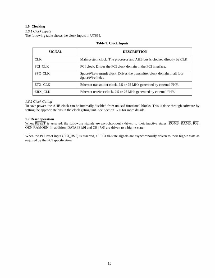
1.6 Clocking
1.6.1 Clock InputsThe following table shows the clock inputs in UT699.
1.6.2 Clock GatingTo save power, the AHB clock can be internally disabled from unused functional blocks. This is done through software bysetting the appropriate bits in the clock gating unit. See Section 17.0 for more details.
1.7 Reset operationWhen RESET is asserted, the following signals are asynchronously driven to their inactive states: ROMS, RAMS, IOS,OEN RAMOEN. In addition, DATA [31:0] and CB [7:0] are driven to a high-z state.
When the PCI reset input (PCI_RST) is asserted, all PCI tri-state signals are asynchronously driven to their high-z state asrequired by the PCI specification.
Table 5. Clock Inputs
SIGNAL DESCRIPTION
CLK Main system clock. The processor and AHB bus is clocked directly by CLK
PCI_CLK PCI clock. Drives the PCI clock domain in the PCI interface.
SPC_CLK SpaceWire transmit clock. Drives the transmitter clock domain in all four SpaceWire links.
ETX_CLK Ethernet transmitter clock. 2.5 or 25 MHz generated by external PHY.
ERX_CLK Ethernet receiver clock. 2.5 or 25 MHz generated by external PHY.
17
2.0 LEON 3FT SPARC V8 32-bit Microprocessor
2.1 Overview
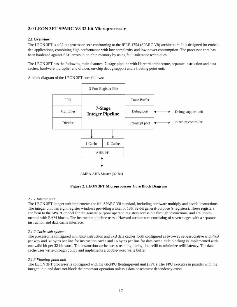
The LEON 3FT is a 32-bit processor core conforming to the IEEE-1754 (SPARC V8) architecture. It is designed for embed-ded applications, combining high performance with low complexity and low power consumption. The processor core has been hardened against SEU errors in on-chip memory by using fault-tolerance techniques.
The LEON 3FT has the following main features: 7-stage pipeline with Harvard architecture, separate instruction and data caches, hardware multiplier and divider, on-chip debug support and a floating point unit.
A block diagram of the LEON 3FT core follows:
2.1.1 Integer unitThe LEON 3FT integer unit implements the full SPARC V8 standard, including hardware multiply and divide instructions. The integer unit has eight register windows providing a total of 136, 32-bit general-purpose (r registers). These registers conform to the SPARC model for the general purpose operand registers accessible through instructions, and are imple-mented with RAM blocks. The instruction pipeline uses a Harvard architecture consisting of seven stages with a separate instruction and data cache interface.
2.1.2 Cache sub-systemThe processor is configured with 8kB instruction and 8kB data caches, both configured as two-way set-associative with 4kB per way and 32 bytes per line for instruction cache and 16 bytes per line for data cache. Sub-blocking is implemented with one valid bit per 32-bit word. The instruction cache uses streaming during line-refill to minimize refill latency. The data cache uses write-through policy and implements a double-word write buffer.
2.1.3 Floating-point unitThe LEON 3FT processor is configured with the GRFPU floating-point unit (FPU). The FPU executes in parallel with the integer unit, and does not block the processor operation unless a data or resource dependency exists.
Integer Pipeline
I-Cache D-Cache
3-Port Register File
AMBA AHB Master (32-bit)
AHB I/F
7-Stage
Interrupt controller
Multiplier
Divider
FPU Trace Buffer
Debug port
Interrupt port
Debug support unit
Figure 2. LEON 3FT Microprocessor Core Block Diagram
18
2.1.4 On-chip debug supportThe LEON 3FT pipeline includes functionality to allow non-intrusive debugging on target hardware. Full access to all pro-cessor registers and cache memory is provided through the debug support unit (DSU). To aid software debugging, two hard-ware watchpoint registers are implemented. Each register can cause a breakpoint trap on an arbitrary instruction or data address range. When the DSU is enabled, the watchpoints can be used to enter debug mode. The DSU also allows single stepping, instruction tracing and hardware breakpoint/watchpoint control. An internal trace buffer monitors and stores exe-cuted instructions which can later be read out over the debug interface.
2.1.5 InterruptsLEON 3FT supports the SPARC V8 trap model with a total of 15 asynchronous interrupts. The interrupt interface provides functionality to both generate and acknowledge interrupts.
2.1.6 AMBA interfaceThe cache system implements an AMBA AHB master to load and store data to/from the caches. The interface is compliant with the AMBA-2.0 standard. During line refill, incremental bursts are generated to optimize the data transfer.
2.1.7 Power-down modeThe LEON 3FT processor core implements a power-down mode, which halts the pipeline and caches until the next interrupt. This is an efficient way to minimize power-consumption when the application is idle.
2.2 LEON 3FT integer unit
2.2.1 OverviewThe LEON 3FT integer unit implements the integer part of the SPARC V8 instruction set. The implementation is focused on high performance and low complexity. The LEON 3FT integer unit has the following main features:
• 7-stage instruction pipeline• Separate instruction and data cache interface• Eight register windows to access the 136 r registers• Hardware multiplier with 5 clocks latency• Radix-2 divider (non-restoring)• Single-vector trapping for reduced code size
19
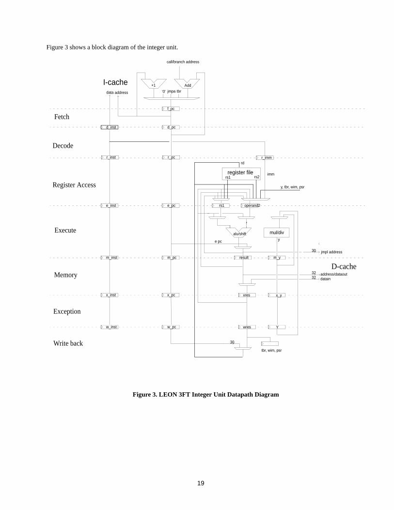
Figure 3 shows a block diagram of the integer unit.
Figure 3. LEON 3FT Integer Unit Datapath Diagram
alu/shift mul/divy
register file
D-cacheaddress/dataoutdatain
3232
operand2rs1
imm
Ywres
result m_y
Decode
Execute
Memory
Write back
rs2rs1
rd
tbr, wim, psr
30 jmpl address
e pc
30
+1
d_pc
jmpa
f_pc
Add
call/branch address
tbr‘0’
e_pc
m_pc
w_pc
d_inst
e_inst
m_inst
w_inst
Fetch
I-cacheaddressdata
Register Access
x_yxres
Exception
x_pcx_inst
r_pcr_inst
y, tbr, wim, psr
r_imm
20
2.2.2 Instruction pipelineThe LEON 3FT integer unit uses a single instruction issue pipeline with seven stages:
1. FE (Instruction Fetch): If the instruction cache is enabled and a cache hit occurs, the instruction is fetched from the instruction cache. Otherwise, the fetch is forwarded to the memory controller. The instruction is valid at the end of this stage and is latched inside the IU.
2. DE (Decode): The instruction is decoded and the CALL or branch target address is generated.
3. RA (Register Access): Operands are read from the register file or from internal data bypasses.
4. EX (Execute): ALU, logical, and shift operations are performed. For memory operations (e.g. LD/ST) and JMPL/RETT instructions, the address is generated.
5. ME (Memory): Data cache is accessed. If a data cache miss occurs, data is accessed from system memory and the cache is updated. Store data read out in the execution stage is written to the data cache at this time.
6. XC (Exception) Traps and interrupts are resolved. For cache reads, the data is aligned as appropriate.
7. WR (Write): The result of any ALU, logical, shift, or cache operations are written back to the register file.
Table 6 lists the cycles per instruction (assuming cache hit, and no integer condition codes or load interlock exist):
2.2.3 SPARC implementor’s IDAeroflex Gaisler is assigned number 15 (0x0F) as SPARC implementor’s identification. This value is hard-coded into bits 31:28 in the processor state register (PSR:impl). The version number for LEON 3FT is 3, which is hard-coded in to bits 27:24 of the PSR (PSR:ver).
2.2.4 Divide instructionsFull support for SPARC V8 divide instructions is provided via instruction SDIV, UDIV, SDIVCC and UDIVCC. The divide instructions perform a 64-by-32 bit divide and produce a 32-bit result. Rounding and overflow detection is performed as defined in the SPARC V8 standard.
Table 6. Instruction Timing
INSTRUCTION CYCLES
JMPL, RETT 3
Double load 2
Single store 2
Double store 3
SMUL/UMUL 5
SDIV/UDIV 35
Taken Trap 5
Atomic load/store 3
All other instructions 1
21
2.2.5 Multiply instructionsThe LEON 3FT processor supports the SPARC integer multiply instructions UMUL, SMUL UMULCC and SMULCC. These instructions perform 32x32-bit integer multiplication producing a 64-bit result. SMUL and SMULCC perform signed multiplication while UMUL and UMULCC perform unsigned multiplication. UMULCC and SMULCC also set the condi-tion codes of the PSR to reflect the result of the operation. The multiply instructions are performed using a 16x16 signed hardware multiplier, which is iterated four times. To improve timing, the 16x16 multiplier is implemented a with a pipeline register stage.
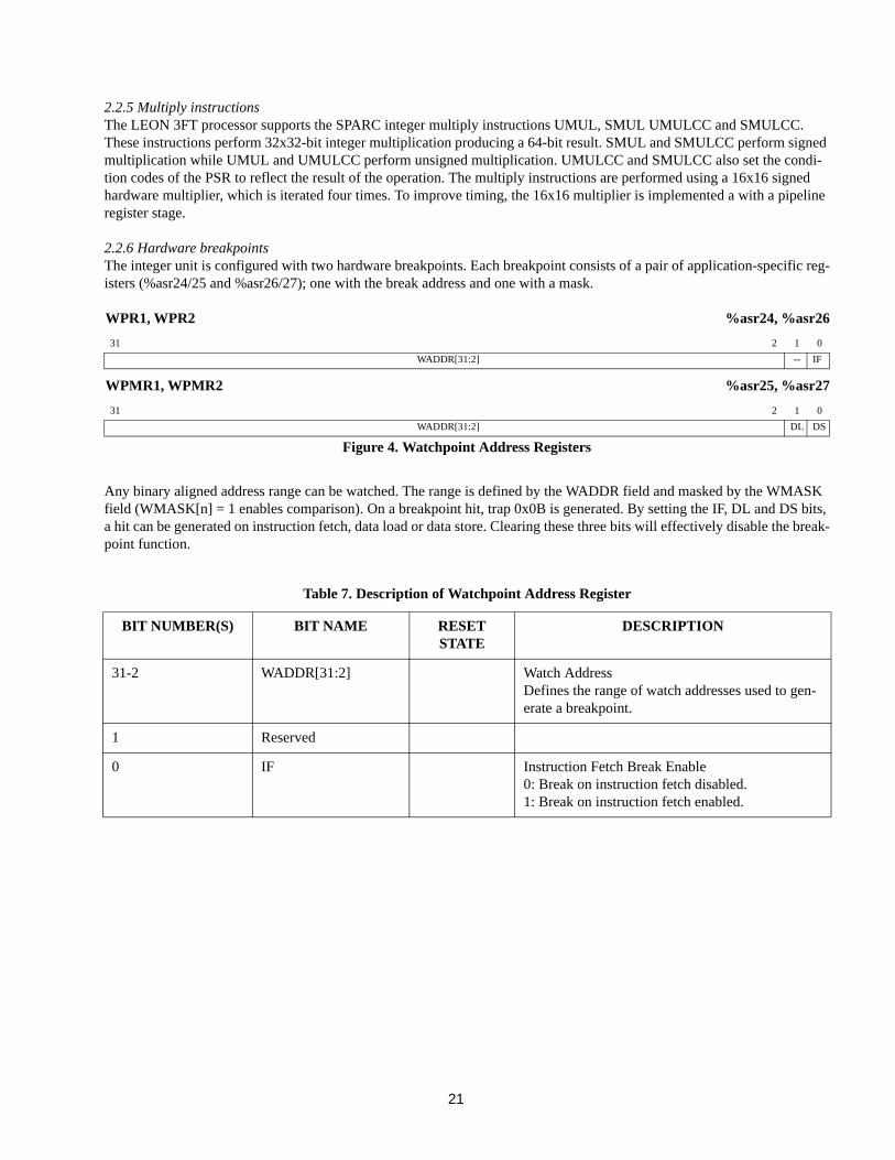
2.2.6 Hardware breakpointsThe integer unit is configured with two hardware breakpoints. Each breakpoint consists of a pair of application-specific reg-isters (%asr24/25 and %asr26/27); one with the break address and one with a mask.
WPR1, WPR2 %asr24, %asr26
WPMR1, WPMR2 %asr25, %asr27
Any binary aligned address range can be watched. The range is defined by the WADDR field and masked by the WMASK field (WMASK[n] = 1 enables comparison). On a breakpoint hit, trap 0x0B is generated. By setting the IF, DL and DS bits, a hit can be generated on instruction fetch, data load or data store. Clearing these three bits will effectively disable the break-point function.
31 2 1 0
WADDR[31:2] -- IF
31 2 1 0
WADDR[31:2] DL DS
Figure 4. Watchpoint Address Registers
Table 7. Description of Watchpoint Address Register
BIT NUMBER(S) BIT NAME RESET STATE
DESCRIPTION
31-2 WADDR[31:2] Watch AddressDefines the range of watch addresses used to gen-erate a breakpoint.
1 Reserved
0 IF Instruction Fetch Break Enable0: Break on instruction fetch disabled.1: Break on instruction fetch enabled.
22
2.2.7 Instruction trace bufferThe instruction trace buffer consists of a circular buffer that stores executed instructions. The trace buffer operation is con-trolled through the debug support interface and does not affect processor operation. The size of the trace buffer is 128 lines deep and 128 bits wide. The buffer stores the following information:
• Instruction address and opcode• Instruction result• Load/store data and address• Trap information• 30-bit time tag
The operation and control of the trace buffer is further described in Chapter 14.0, Hardware Debug Support.
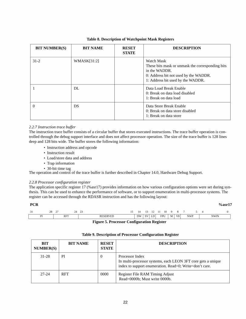
2.2.8 Processor configuration registerThe application specific register 17 (%asr17) provides information on how various configuration options were set during syn-thesis. This can be used to enhance the performance of software, or to support enumeration in multi-processor systems. The register can be accessed through the RDASR instruction and has the following layout:
Table 8. Description of Watchpoint Mask Registers
BIT NUMBER(S) BIT NAME RESET STATE
DESCRIPTION
31-2 WMASK[31:2] Watch MaskThese bits mask or unmask the corresponding bits in the WADDR.0: Address bit not used by the WADDR.1: Address bit used by the WADDR.
1 DL Data Load Break Enable0: Break on data load disabled1: Break on data load
0 DS Data Store Break Enable0: Break on data store disabled1: Break on data store
Table 9. Description of Processor Configuration Register
BIT NUMBER(S)
BIT NAME RESET STATE
DESCRIPTION
31-28 PI 0 Processor IndexIn multi-processor systems, each LEON 3FT core gets a unique index to support enumeration. Read=0; Write=don’t care.
27-24 RFT 0000 Register File RAM Timing AdjustRead=0000b; Must write 0000b.
PCR %asr17
31 28 27 24 23 15 14 13 12 11 10 9 8 7 5 4 0
PI RFT RESERVED DW SV LD FPU M V8 NWP NWIN
Figure 5. Processor Configuration Register
23
BIT NUMBER(S)
BIT NAME RESET STATE
DESCRIPTION
23-15 Reserved
14 DW 0 Disable Write Error Trap0: Write error trap (tt=0x2b) allowed.1: Write error trap (tt=0x2b) ignored.
13 SV 0 Single-Vector Trapping Enable0: Single-vector trapping disabled.1: Single-vector trapping enabled.
12 LD 0 Load Delay0: One-cycle load delay is used.1: Two-cycle load delay is used.Read=0; Write=don’t care.
11-10 FPU 01 Floating Point Implementation00: No FPU01: GRFPU10: Meiko FPU11: GRFPU-LiteRead=01; Write=don’t care.
9 M 0 MAC Implementation0: Optional multiply-accumulate (MAC) instruction not available.1: Optional multiply-accumulate (MAC) instruction is available.Read=0; Write=don’t care.
8 V8 1 Multiply and Divide Implementation0: SPARC V8 multiply and divide instructions not available.1: SPARC V8 multiply and divide instructions are available.Read=1; Write=don’t care.
7-5 NWP 010 Watchpoint ImplementationNumber of implemented watchpoints.Read=010b; Write=don’t care.
4-0 NWIN 00111 Register Window ImplementationNumber of implemented registers windows corresponds to NWIN+1.Read=00111b; Write=don’t care.
Table 9. Description of Processor Configuration Register
24
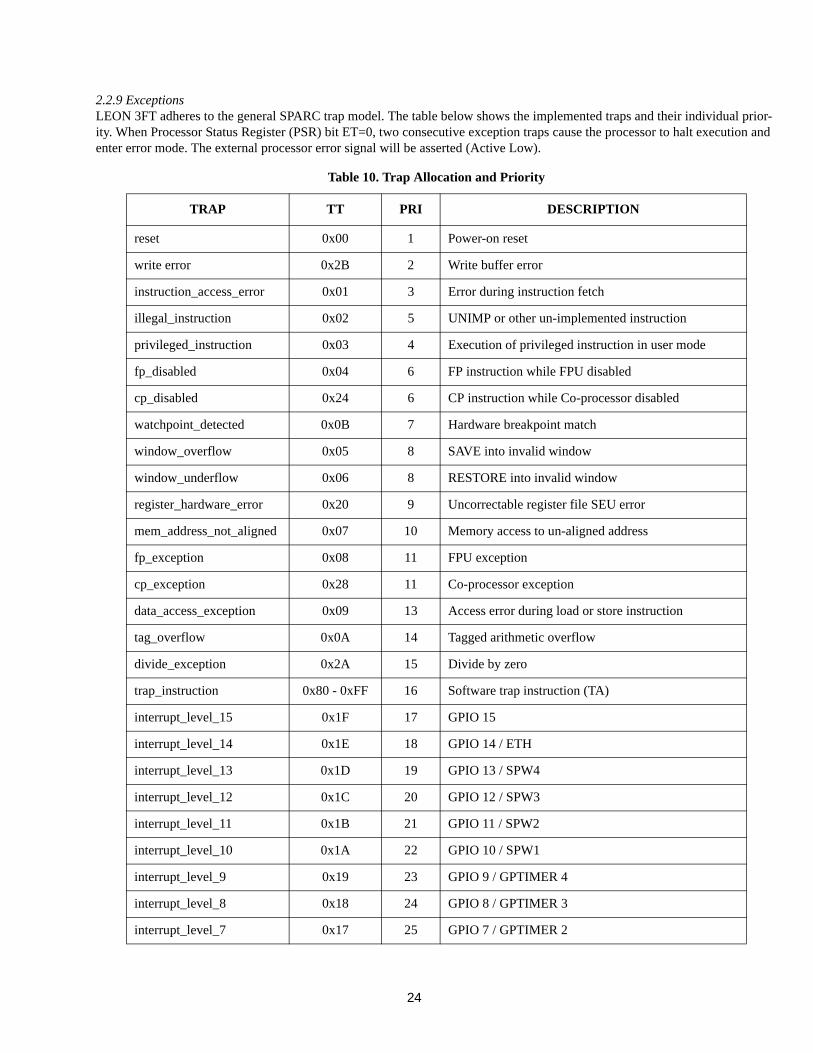
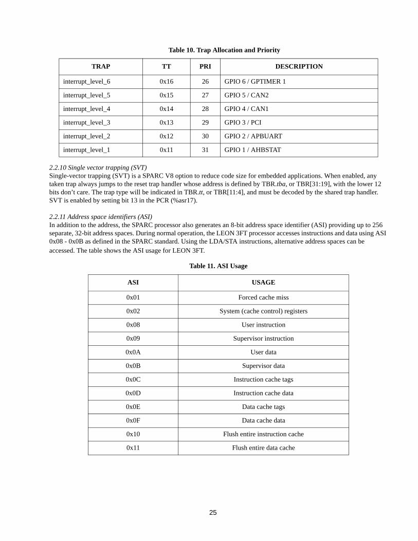
2.2.9 ExceptionsLEON 3FT adheres to the general SPARC trap model. The table below shows the implemented traps and their individual prior-ity. When Processor Status Register (PSR) bit ET=0, two consecutive exception traps cause the processor to halt execution and enter error mode. The external processor error signal will be asserted (Active Low).
Table 10. Trap Allocation and Priority
TRAP TT PRI DESCRIPTION
reset 0x00 1 Power-on reset
write error 0x2B 2 Write buffer error
instruction_access_error 0x01 3 Error during instruction fetch
illegal_instruction 0x02 5 UNIMP or other un-implemented instruction
privileged_instruction 0x03 4 Execution of privileged instruction in user mode
fp_disabled 0x04 6 FP instruction while FPU disabled
cp_disabled 0x24 6 CP instruction while Co-processor disabled
watchpoint_detected 0x0B 7 Hardware breakpoint match
window_overflow 0x05 8 SAVE into invalid window
window_underflow 0x06 8 RESTORE into invalid window
register_hardware_error 0x20 9 Uncorrectable register file SEU error
mem_address_not_aligned 0x07 10 Memory access to un-aligned address
fp_exception 0x08 11 FPU exception
cp_exception 0x28 11 Co-processor exception
data_access_exception 0x09 13 Access error during load or store instruction
tag_overflow 0x0A 14 Tagged arithmetic overflow
divide_exception 0x2A 15 Divide by zero
trap_instruction 0x80 - 0xFF 16 Software trap instruction (TA)
interrupt_level_15 0x1F 17 GPIO 15
interrupt_level_14 0x1E 18 GPIO 14 / ETH
interrupt_level_13 0x1D 19 GPIO 13 / SPW4
interrupt_level_12 0x1C 20 GPIO 12 / SPW3
interrupt_level_11 0x1B 21 GPIO 11 / SPW2
interrupt_level_10 0x1A 22 GPIO 10 / SPW1
interrupt_level_9 0x19 23 GPIO 9 / GPTIMER 4
interrupt_level_8 0x18 24 GPIO 8 / GPTIMER 3
interrupt_level_7 0x17 25 GPIO 7 / GPTIMER 2
25
2.2.10 Single vector trapping (SVT)Single-vector trapping (SVT) is a SPARC V8 option to reduce code size for embedded applications. When enabled, any taken trap always jumps to the reset trap handler whose address is defined by TBR.tba, or TBR[31:19], with the lower 12 bits don’t care. The trap type will be indicated in TBR.tt, or TBR[11:4], and must be decoded by the shared trap handler. SVT is enabled by setting bit 13 in the PCR (%asr17).
2.2.11 Address space identifiers (ASI)In addition to the address, the SPARC processor also generates an 8-bit address space identifier (ASI) providing up to 256 separate, 32-bit address spaces. During normal operation, the LEON 3FT processor accesses instructions and data using ASI 0x08 - 0x0B as defined in the SPARC standard. Using the LDA/STA instructions, alternative address spaces can be accessed. The table shows the ASI usage for LEON 3FT.
TRAP TT PRI DESCRIPTION
interrupt_level_6 0x16 26 GPIO 6 / GPTIMER 1
interrupt_level_5 0x15 27 GPIO 5 / CAN2
interrupt_level_4 0x14 28 GPIO 4 / CAN1
interrupt_level_3 0x13 29 GPIO 3 / PCI
interrupt_level_2 0x12 30 GPIO 2 / APBUART
interrupt_level_1 0x11 31 GPIO 1 / AHBSTAT
Table 11. ASI Usage
ASI USAGE
0x01 Forced cache miss
0x02 System (cache control) registers
0x08 User instruction
0x09 Supervisor instruction
0x0A User data
0x0B Supervisor data
0x0C Instruction cache tags
0x0D Instruction cache data
0x0E Data cache tags
0x0F Data cache data
0x10 Flush entire instruction cache
0x11 Flush entire data cache
Table 10. Trap Allocation and Priority
26
2.2.12 Power-downThe processor can be configured to include a power-down feature to minimize power consumption during idle periods. The power-down mode is entered by performing a WRASR instruction to%asr19:
wr %g0,%asr19 // write 0x0 to%asr19
During power-down, the pipeline is halted until the next interrupt occurs. Signals inside the processor pipeline and caches are then static, reducing power consumption from dynamic switching.
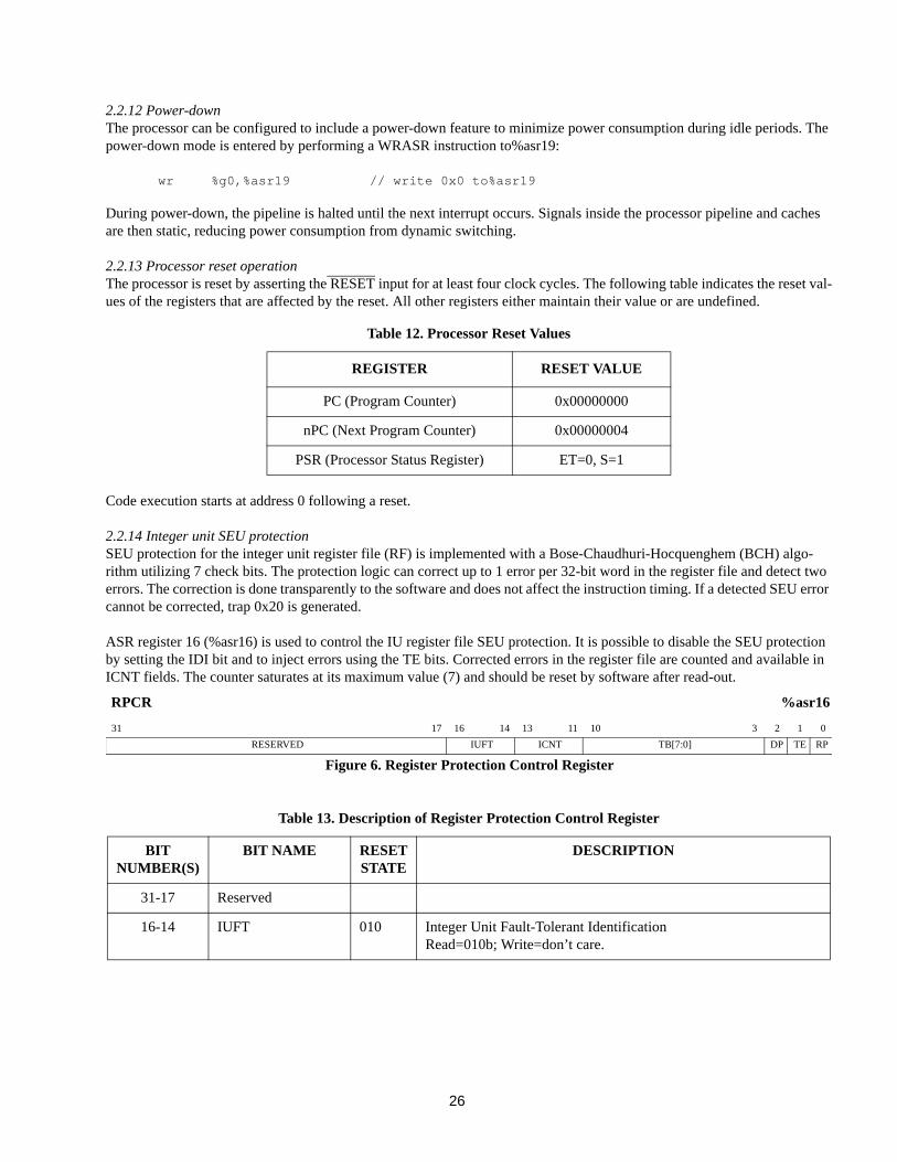
2.2.13 Processor reset operationThe processor is reset by asserting the RESET input for at least four clock cycles. The following table indicates the reset val-ues of the registers that are affected by the reset. All other registers either maintain their value or are undefined.
Code execution starts at address 0 following a reset.
2.2.14 Integer unit SEU protectionSEU protection for the integer unit register file (RF) is implemented with a Bose-Chaudhuri-Hocquenghem (BCH) algo-rithm utilizing 7 check bits. The protection logic can correct up to 1 error per 32-bit word in the register file and detect two errors. The correction is done transparently to the software and does not affect the instruction timing. If a detected SEU error cannot be corrected, trap 0x20 is generated.
ASR register 16 (%asr16) is used to control the IU register file SEU protection. It is possible to disable the SEU protection by setting the IDI bit and to inject errors using the TE bits. Corrected errors in the register file are counted and available in ICNT fields. The counter saturates at its maximum value (7) and should be reset by software after read-out.
Table 12. Processor Reset Values
REGISTER RESET VALUE
PC (Program Counter) 0x00000000
nPC (Next Program Counter) 0x00000004
PSR (Processor Status Register) ET=0, S=1
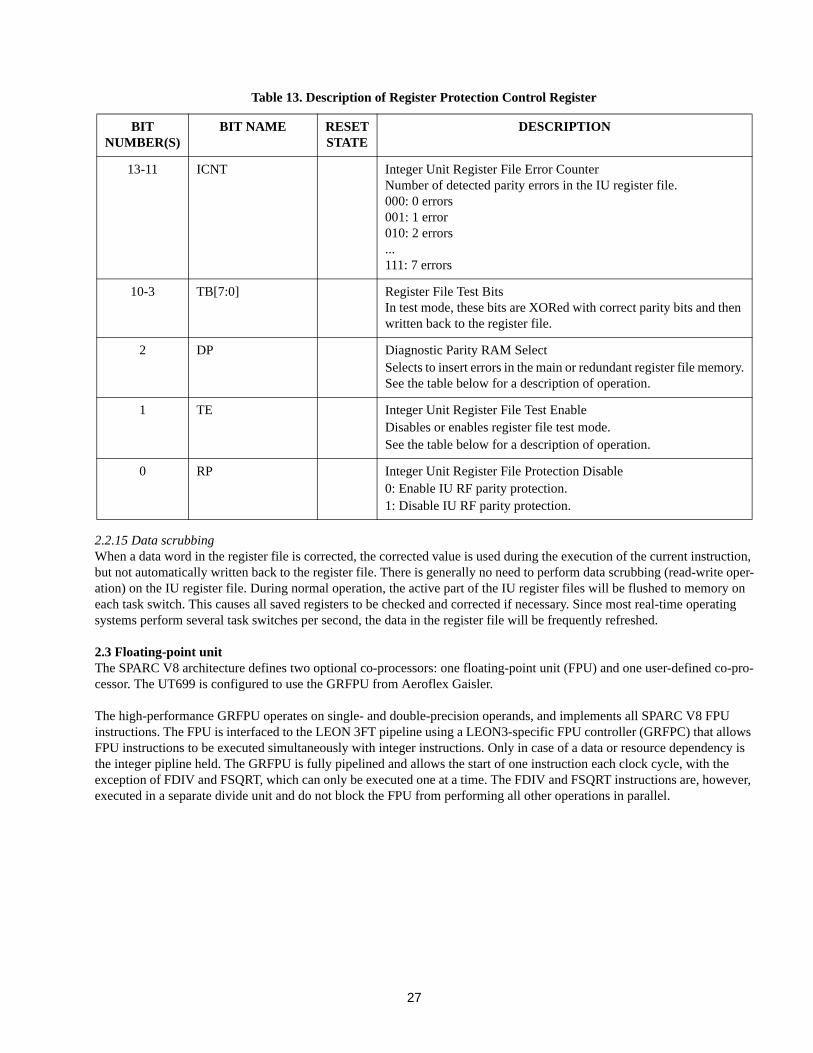
Table 13. Description of Register Protection Control Register
BIT NUMBER(S)
BIT NAME RESET STATE
DESCRIPTION
31-17 Reserved
16-14 IUFT 010 Integer Unit Fault-Tolerant IdentificationRead=010b; Write=don’t care.
RPCR %asr16
31 17 16 14 13 11 10 3 2 1 0
RESERVED IUFT ICNT TB[7:0] DP TE RP
Figure 6. Register Protection Control Register
27
2.2.15 Data scrubbingWhen a data word in the register file is corrected, the corrected value is used during the execution of the current instruction, but not automatically written back to the register file. There is generally no need to perform data scrubbing (read-write oper-ation) on the IU register file. During normal operation, the active part of the IU register files will be flushed to memory on each task switch. This causes all saved registers to be checked and corrected if necessary. Since most real-time operating systems perform several task switches per second, the data in the register file will be frequently refreshed.
2.3 Floating-point unitThe SPARC V8 architecture defines two optional co-processors: one floating-point unit (FPU) and one user-defined co-pro-cessor. The UT699 is configured to use the GRFPU from Aeroflex Gaisler.
The high-performance GRFPU operates on single- and double-precision operands, and implements all SPARC V8 FPU instructions. The FPU is interfaced to the LEON 3FT pipeline using a LEON3-specific FPU controller (GRFPC) that allows FPU instructions to be executed simultaneously with integer instructions. Only in case of a data or resource dependency is the integer pipline held. The GRFPU is fully pipelined and allows the start of one instruction each clock cycle, with the exception of FDIV and FSQRT, which can only be executed one at a time. The FDIV and FSQRT instructions are, however, executed in a separate divide unit and do not block the FPU from performing all other operations in parallel.
BIT NUMBER(S)
BIT NAME RESET STATE
DESCRIPTION
13-11 ICNT Integer Unit Register File Error CounterNumber of detected parity errors in the IU register file.000: 0 errors001: 1 error010: 2 errors...111: 7 errors
10-3 TB[7:0] Register File Test BitsIn test mode, these bits are XORed with correct parity bits and then written back to the register file.
2 DP Diagnostic Parity RAM SelectSelects to insert errors in the main or redundant register file memory.See the table below for a description of operation.
1 TE Integer Unit Register File Test EnableDisables or enables register file test mode.See the table below for a description of operation.
0 RP Integer Unit Register File Protection Disable0: Enable IU RF parity protection.1: Disable IU RF parity protection.
Table 13. Description of Register Protection Control Register
28
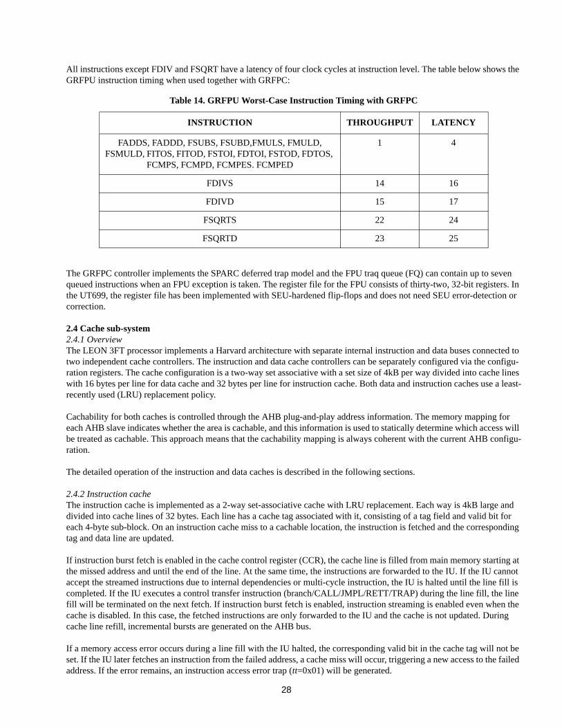
All instructions except FDIV and FSQRT have a latency of four clock cycles at instruction level. The table below shows the GRFPU instruction timing when used together with GRFPC:
The GRFPC controller implements the SPARC deferred trap model and the FPU traq queue (FQ) can contain up to seven queued instructions when an FPU exception is taken. The register file for the FPU consists of thirty-two, 32-bit registers. In the UT699, the register file has been implemented with SEU-hardened flip-flops and does not need SEU error-detection or correction.
2.4 Cache sub-system2.4.1 OverviewThe LEON 3FT processor implements a Harvard architecture with separate internal instruction and data buses connected to two independent cache controllers. The instruction and data cache controllers can be separately configured via the configu-ration registers. The cache configuration is a two-way set associative with a set size of 4kB per way divided into cache lines with 16 bytes per line for data cache and 32 bytes per line for instruction cache. Both data and instruction caches use a least-recently used (LRU) replacement policy.
Cachability for both caches is controlled through the AHB plug-and-play address information. The memory mapping for each AHB slave indicates whether the area is cachable, and this information is used to statically determine which access will be treated as cachable. This approach means that the cachability mapping is always coherent with the current AHB configu-ration.
The detailed operation of the instruction and data caches is described in the following sections.
2.4.2 Instruction cacheThe instruction cache is implemented as a 2-way set-associative cache with LRU replacement. Each way is 4kB large and divided into cache lines of 32 bytes. Each line has a cache tag associated with it, consisting of a tag field and valid bit for each 4-byte sub-block. On an instruction cache miss to a cachable location, the instruction is fetched and the corresponding tag and data line are updated.
If instruction burst fetch is enabled in the cache control register (CCR), the cache line is filled from main memory starting at the missed address and until the end of the line. At the same time, the instructions are forwarded to the IU. If the IU cannot accept the streamed instructions due to internal dependencies or multi-cycle instruction, the IU is halted until the line fill is completed. If the IU executes a control transfer instruction (branch/CALL/JMPL/RETT/TRAP) during the line fill, the line fill will be terminated on the next fetch. If instruction burst fetch is enabled, instruction streaming is enabled even when the cache is disabled. In this case, the fetched instructions are only forwarded to the IU and the cache is not updated. During cache line refill, incremental bursts are generated on the AHB bus.
If a memory access error occurs during a line fill with the IU halted, the corresponding valid bit in the cache tag will not be set. If the IU later fetches an instruction from the failed address, a cache miss will occur, triggering a new access to the failed address. If the error remains, an instruction access error trap (tt=0x01) will be generated.
Table 14. GRFPU Worst-Case Instruction Timing with GRFPC
INSTRUCTION THROUGHPUT LATENCY
FADDS, FADDD, FSUBS, FSUBD,FMULS, FMULD, FSMULD, FITOS, FITOD, FSTOI, FDTOI, FSTOD, FDTOS,
FCMPS, FCMPD, FCMPES. FCMPED
1 4
FDIVS 14 16
FDIVD 15 17
FSQRTS 22 24
FSQRTD 23 25
29
2.4.3 Data cacheThe data cache is configured identical to the instruction cache with two ways of 4kB, 16 bytes/line and LRU replacement. On a data cache read-miss to a cachable location, 4 bytes of data are loaded into the cache from main memory. The write pol-icy for stores is write-through with no-allocate on a write miss. If a memory access error occurs during a data load, the corre-sponding valid bit in the cache tag will not be set and a data access error trap (tt=0x09) will be generated.
2.4.4 Write bufferThe write buffer (WRB) consists of three 32-bit registers used to temporarily hold store data until it is sent to the destination device. For half-word or byte stores, the stored data is replicated into proper byte alignment for writing to a word-addressed device before being loaded into one of the WRB registers. The WRB is emptied prior to a load-miss cache-fill sequence to avoid any stale data from being written into the data cache.
Since the processor executes in parallel with the write buffer, a write error will not cause an exception to the store instruc-tion. Depending on memory and cache activity, the write cycle may not occur until several clock cycles after the store instruction has completed. If a write error occurs, the currently executing instruction will take trap 0x2B.
Note: The 0x2B trap handler should flush the data cache, since a write hit would update the cache while the memory would keep the old value due the write error.
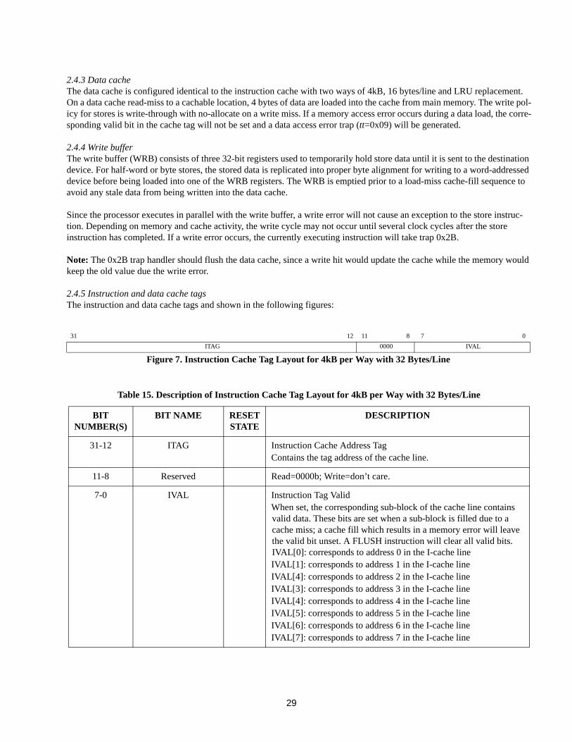
2.4.5 Instruction and data cache tagsThe instruction and data cache tags and shown in the following figures:
Table 15. Description of Instruction Cache Tag Layout for 4kB per Way with 32 Bytes/Line
BIT NUMBER(S)
BIT NAME RESET STATE
DESCRIPTION
31-12 ITAG Instruction Cache Address TagContains the tag address of the cache line.
11-8 Reserved Read=0000b; Write=don’t care.
7-0 IVAL Instruction Tag ValidWhen set, the corresponding sub-block of the cache line contains valid data. These bits are set when a sub-block is filled due to a cache miss; a cache fill which results in a memory error will leave the valid bit unset. A FLUSH instruction will clear all valid bits. IVAL[0]: corresponds to address 0 in the I-cache lineIVAL[1]: corresponds to address 1 in the I-cache lineIVAL[4]: corresponds to address 2 in the I-cache lineIVAL[3]: corresponds to address 3 in the I-cache lineIVAL[4]: corresponds to address 4 in the I-cache lineIVAL[5]: corresponds to address 5 in the I-cache lineIVAL[6]: corresponds to address 6 in the I-cache lineIVAL[7]: corresponds to address 7 in the I-cache line
31 12 11 8 7 0
ITAG 0000 IVAL
Figure 7. Instruction Cache Tag Layout for 4kB per Way with 32 Bytes/Line
30
2.4.6 Cache flushingBoth instruction and data caches are flushed by executing the FLUSH instruction or by writing to any location with ASI=0x10 or ASI=0x11. In addition, the entire instruction cache is flushed by setting the FI bit in the cache control register (CCR). The entire data cache is flushed by seting the FD bit in the CCR. Cache flushing takes one cycle per cache line, dur-ing which, the IU will not be halted and the caches are disabled. When the flush operation is completed, the cache resumes the state (disabled, enabled or frozen) indicated in the cache control register. Diagnostic access to the cache is not possible during a FLUSH operation and will cause a data exception (tt=0x09) if attempted.
2.4.7 Diagnostic cache accessTags and data in the instruction and data cache can be accessed through ASI address space 0x0C, 0x0D, 0x0E and 0x0F by executing LDA and STA instructions. The ITAG and DTAG fields of the cache tag define the upper 20 bits of the address, while the twelve (12) least significant bits of the address correspond to the index of the cache set.
2.4.7.1 Diagnostic reads of instruction and data cacheCache tags are read by executing an LDA instruction with ASI=0x0C for instruction cache tags and ASI=0x0E for data cache tags. A cache line and set are indexed by the address bits making up the cache offset and the least significant bits of the address bits making up the address tag. Similarly, the data sub-blocks may be read by executing an LDA instruction with ASI=0x0D for instruction cache data and ASI=0x0F for data cache data. The sub-block to be read in the indexed cache line and set is selected 64, the regaddr field of the LDA or STA instruction.
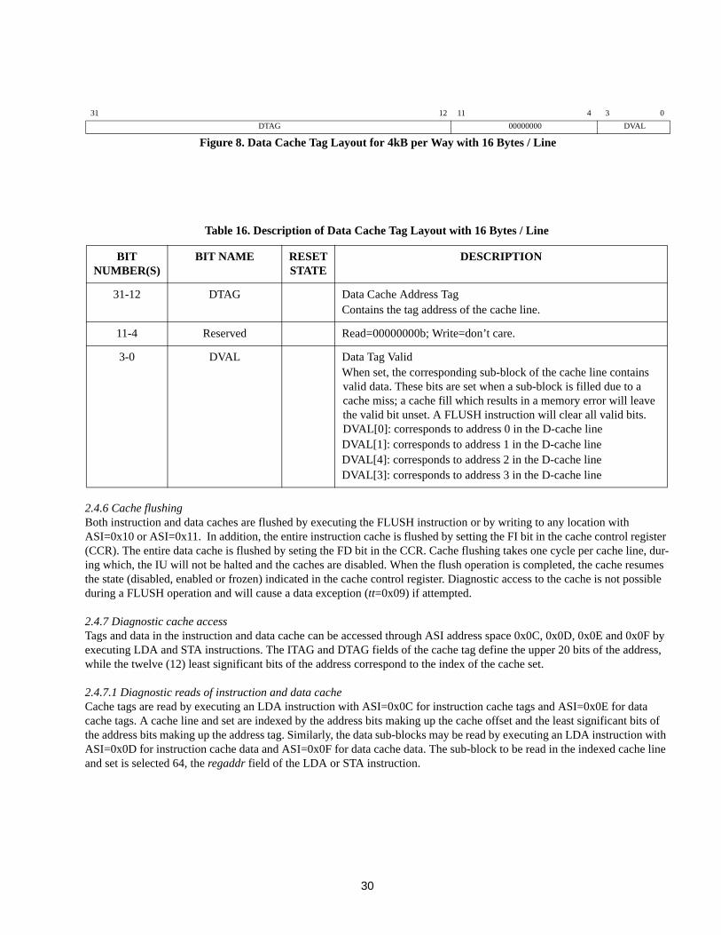
Table 16. Description of Data Cache Tag Layout with 16 Bytes / Line
BIT NUMBER(S)
BIT NAME RESET STATE
DESCRIPTION
31-12 DTAG Data Cache Address TagContains the tag address of the cache line.
11-4 Reserved Read=00000000b; Write=don’t care.
3-0 DVAL Data Tag ValidWhen set, the corresponding sub-block of the cache line contains valid data. These bits are set when a sub-block is filled due to a cache miss; a cache fill which results in a memory error will leave the valid bit unset. A FLUSH instruction will clear all valid bits. DVAL[0]: corresponds to address 0 in the D-cache lineDVAL[1]: corresponds to address 1 in the D-cache lineDVAL[4]: corresponds to address 2 in the D-cache lineDVAL[3]: corresponds to address 3 in the D-cache line
31 12 11 4 3 0
DTAG 00000000 DVAL
Figure 8. Data Cache Tag Layout for 4kB per Way with 16 Bytes / Line
31
2.4.7.2 Diagnostic writes to instruction and data cacheCache tags can be directly written to by executing a STA instruction with ASI=0xC for the instruction cache tags and ASI=0x0E for the data cache tags. The cache line and set are indexed by the address bits making up the cache offset and the least significant bits of the address bits making up the address tag. D[31:10] is written into the ATAG filed and the valid bits are written with D[7:0] of the write data for instruction cache and D[3:0] for data cache. Bit D[9] is written into the LRR bit (disabled) and D[8] is written into the lock bit (disabled). The data sub-blocks can be directly written by executing a STA instruction with ASI=0xD for the instruction cache data and ASI=0xF for the data cache data. The sub-block to be read in the indexed cache line and set is selected by A[4:2].
2.4.8 Cache control registerThe operation of the instruction and data caches is controlled through a common Cache Control Register (CCR) as shown in Figure 9. Each cache can operate in one of three modes: disabled, enabled or frozen, as determined by the DCS or ICS fields. If disabled, no cache operation is performed and load and store requests are passed directly to the memory controller. If enabled, the cache operates as described above. In the frozen state, the cache is accessed and kept synchronized to the main memory as if it were enabled, but no new lines are allocated on read misses.
Table 17. Description of Cache Control Register
BIT NUMBER(S)
BIT NAME RESET STATE
DESCRIPTION
31-29 Reserved
28 PS Parity Select0: Diagnostic read will return tag or data word.1: Diagnostic read will return the check bits in the bits 3:0.
27-24 TB Test Bits0: No effect.1: Check bits will be XORed with test bits TB during diagnostic. write.
23 Reserved Must write 0.
22 FD Flush Data Cache0: No effect.1: Flush the data cache.Read=0.
21 FI Flush Instruction Cache0: No effect.1: Flush the instruction cache.Read=0.
ASI 0x02 CCR OFFSET 0x00
31 29 28 27 24 23 22 21 20 19 18 17 16 15 14 13 12 11 10 9 8 7 6 5 4 3 2 1 0
RES PS TB -- FD FI FT -- IB IP DP ITE IDE DTE DDE DF IF DCS ICS
Figure 9. Cache Control Register
32
BIT NUMBER(S)
BIT NAME RESET STATE
DESCRIPTION
20-19 FT Fault Tolerant Mode00: No fault-tolerance01: 4-bit parity checking10: Unused11: Unused
18-17 Reserved
16 IB Instruction Burst Fetch0: Disable burst fill during instruction fetch.1: Enable burst fill during instruction fetch.
15 IP Instruction Cache Flush Pending0: Instruction cache flush operation not in progress.1: Instruction cache flush operation is in progress.
14 DP Data Cache Flush Pending0: Data cache flush operation is not in progress.1: Data cache flush operation is in progress.
13-12 ITE Instruction Cache Tag ErrorsNumber of detected parity errors in the instruction tag cache.
11-10 IDE Instruction Cache Data ErrorsNumber of parity errors in the instruction data cache.
9-8 DTE Data Cache Tag ErrorsNumber of detected parity errors in the data tag cache.
7-6 DDE Data Cache Data ErrorsNumber of detected parity errors in the data cache.
5 DF Data Cache Freeze on InterruptData cache response to asynchronous interrupt:0: Normal operation.1: Data cache automatically frozen.
4 IF Instruction Cache Freeze on InterruptInstruction cache response to asynchronous interrupt:0: Normal operation.1: Instruction cache automatically frozen.
3-2 DCS Data Cache StateIndicates the current data cache state:x0: Disabled01: Frozen11: Enabledx=don’t care.
Table 17. Description of Cache Control Register
33
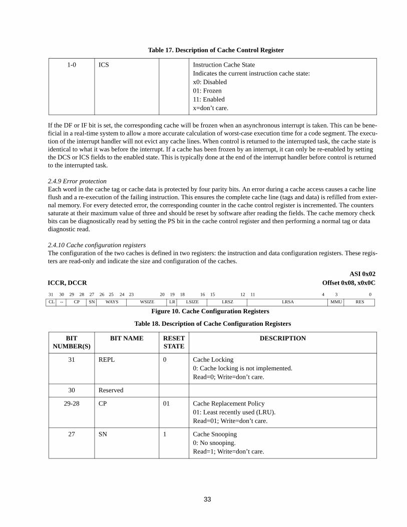
If the DF or IF bit is set, the corresponding cache will be frozen when an asynchronous interrupt is taken. This can be bene-ficial in a real-time system to allow a more accurate calculation of worst-case execution time for a code segment. The execu-tion of the interrupt handler will not evict any cache lines. When control is returned to the interrupted task, the cache state is identical to what it was before the interrupt. If a cache has been frozen by an interrupt, it can only be re-enabled by setting the DCS or ICS fields to the enabled state. This is typically done at the end of the interrupt handler before control is returned to the interrupted task.
2.4.9 Error protectionEach word in the cache tag or cache data is protected by four parity bits. An error during a cache access causes a cache line flush and a re-execution of the failing instruction. This ensures the complete cache line (tags and data) is refilled from exter-nal memory. For every detected error, the corresponding counter in the cache control register is incremented. The counters saturate at their maximum value of three and should be reset by software after reading the fields. The cache memory check bits can be diagnostically read by setting the PS bit in the cache control register and then performing a normal tag or data diagnostic read.
2.4.10 Cache configuration registersThe configuration of the two caches is defined in two registers: the instruction and data configuration registers. These regis-ters are read-only and indicate the size and configuration of the caches.
1-0 ICS Instruction Cache StateIndicates the current instruction cache state:x0: Disabled01: Frozen11: Enabledx=don’t care.
Table 18. Description of Cache Configuration Registers
BIT NUMBER(S)
BIT NAME RESET STATE
DESCRIPTION
31 REPL 0 Cache Locking0: Cache locking is not implemented.Read=0; Write=don’t care.
30 Reserved
29-28 CP 01 Cache Replacement Policy01: Least recently used (LRU).Read=01; Write=don’t care.
27 SN 1 Cache Snooping0: No snooping.Read=1; Write=don’t care.
Table 17. Description of Cache Control Register
ASI 0x02 ICCR, DCCR Offset 0x08, x0x0C
31 30 29 28 27 26 25 24 23 20 19 18 16 15 12 11 4 3 0
CL -- CP SN WAYS WSIZE LR LSIZE LRSZ LRSA MMU RES
Figure 10. Cache Configuration Registers
34
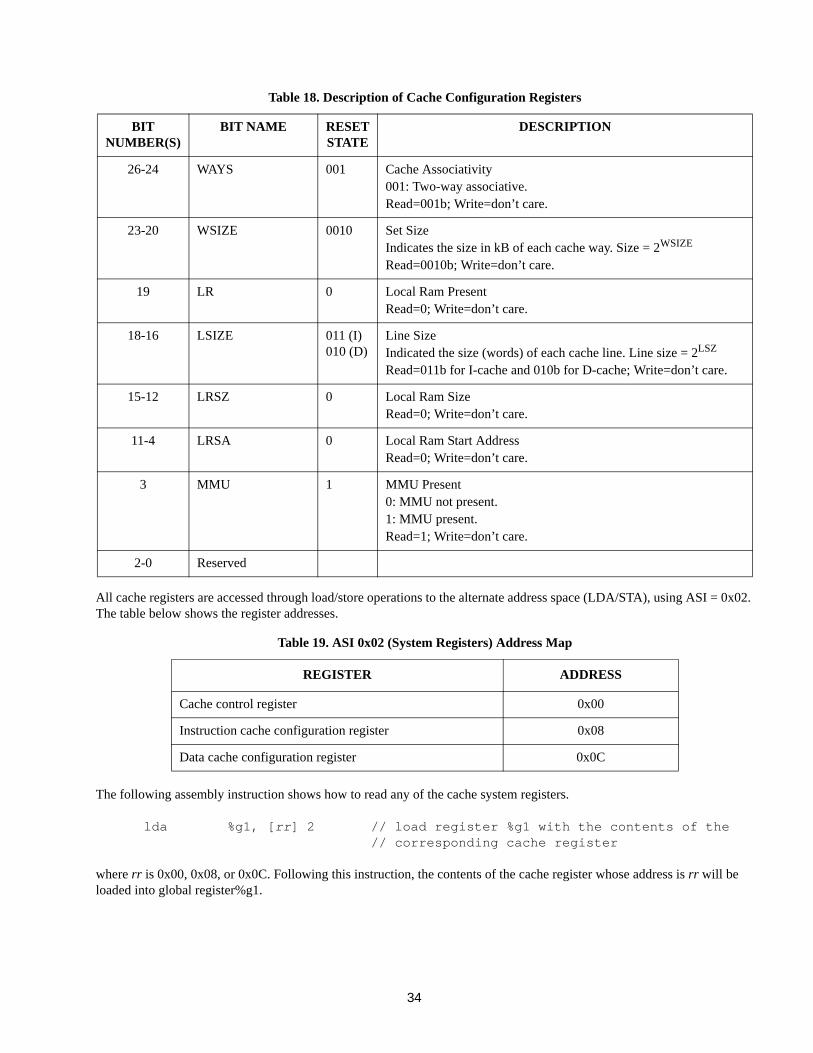
All cache registers are accessed through load/store operations to the alternate address space (LDA/STA), using ASI = 0x02. The table below shows the register addresses.
The following assembly instruction shows how to read any of the cache system registers.
lda %g1, [rr] 2 // load register %g1 with the contents of the// corresponding cache register
where rr is 0x00, 0x08, or 0x0C. Following this instruction, the contents of the cache register whose address is rr will be loaded into global register%g1.
BIT NUMBER(S)
BIT NAME RESET STATE
DESCRIPTION
26-24 WAYS 001 Cache Associativity001: Two-way associative.Read=001b; Write=don’t care.
23-20 WSIZE 0010 Set SizeIndicates the size in kB of each cache way. Size = 2WSIZE
Read=0010b; Write=don’t care.
19 LR 0 Local Ram PresentRead=0; Write=don’t care.
18-16 LSIZE 011 (I)010 (D)
Line SizeIndicated the size (words) of each cache line. Line size = 2LSZ
Read=011b for I-cache and 010b for D-cache; Write=don’t care.
15-12 LRSZ 0 Local Ram SizeRead=0; Write=don’t care.
11-4 LRSA 0 Local Ram Start AddressRead=0; Write=don’t care.
3 MMU 1 MMU Present0: MMU not present.1: MMU present.Read=1; Write=don’t care.
2-0 Reserved
Table 19. ASI 0x02 (System Registers) Address Map
REGISTER ADDRESS
Cache control register 0x00
Instruction cache configuration register 0x08
Data cache configuration register 0x0C
Table 18. Description of Cache Configuration Registers
35
2.4.11 Software considerationAfter reset, the caches are disabled and the value of cache control register (CCR) is 0. Before the caches may be enabled, a flush operation must be performed to initialized (clear) the tags and valid bits. A suitable assembly sequence could be:
flushset 0x81000F,%g1 // load global register %g1 with 0x0081000Fsta %g1, [%g0] 2 // store the contents of %g1 to the CCR
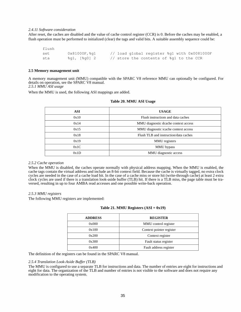
2.5 Memory management unit
A memory management unit (MMU) compatible with the SPARC V8 reference MMU can optionally be configured. Fordetails on operation, see the SPARC V8 manual.2.5.1 MMU ASI usage
When the MMU is used, the following ASI mappings are added.
2.5.2 Cache operationWhen the MMU is disabled, the caches operate normally with physical address mapping. When the MMU is enabled, thecache tags contain the virtual address and include an 8-bit context field. Because the cache is virtually tagged, no extra clockcycles are needed in the case of a cache load hit. In the case of a cache miss or store hit (write-through cache) at least 2 extraclock cycles are used if there is a translation look-aside buffer (TLB) hit. If there is a TLB miss, the page table must be tra-versed, resulting in up to four AMBA read accesses and one possible write-back operation.
2.5.3 MMU registersThe following MMU registers are implemented:
The definition of the registers can be found in the SPARC V8 manual.
2.5.4 Translation Look-Aside Buffer (TLB)The MMU is configured to use a separate TLB for instructions and data. The number of entries are eight for instructions and eight for data. The organization of the TLB and number of entries is not visible to the software and does not require any modification to the operating system.
Table 20. MMU ASI Usage
ASI USAGE
0x10 Flush instructiom and data caches
0x14 MMU diagnostic dcache context access
0x15 MMU diagnostic icache context access
0x18 Flush TLB and instruction/data caches
0x19 MMU registers
0x1C MMU bypass
0x1D MMU diagnostic access
Table 21. MMU Registers (ASI = 0x19)
ADDRESS REGISTER
0x000 MMU control register
0x100 Context pointer register
0x200 Context register
0x300 Fault status register
0x400 Fault address register
36
2.6 RAM usage2.6.1 Integer unit register fileThe integer unit register file has one write port and two read ports, all 39 bits wide. The data is organized as 32-data bits + 7 BCH checksum bits. The register file is implemented with two sets of three RAM blocks. Each set is implementing with 256x48 2-port RAM by concatenating three 256x16 2-port RAM blocks. The 32-bit data is stored in bits [31:0] while the parity bits are stored in [38:32]. Bits [47:39] are unused and tied to ground. The BCH bits are generated as follows:
P0 = D0 ^ D4 ^ D6 ^ D7 ^ D8 ^ D9 ^ D11 ^ D14 ^ D17 ^ D18 ^ D19 ^ D21 ^ D26 ^ D28 ^ D29 ^ D31P1 = D0 ^ D1 ^ D2 ^ D4 ^ D6 ^ D8 ^ D10 ^ D12 ^ D16 ^ D17 ^ D18 ^ D20 ^ D22 ^ D24 ^ D26 ^ D28P2 = D0 ^ D3 ^ D4 ^ D7 ^ D9 ^ D10 ^ D13 ^ D15 ^ D16 ^ D19 ^ D20 ^ D23 ^ D25 ^ D26 ^ D29 ^ D31P3 = D0 ^ D1 ^ D5 ^ D6 ^ D7 ^ D11 ^ D12 ^ D13 ^ D16 ^ D17 ^ D21 ^ D22 ^ D23 ^ D27 ^ D28 ^ D29P4 = D2 ^ D3 ^ D4 ^ D5 ^ D6 ^ D7 ^ D14 ^ D15 ^ D18 ^ D19 ^ D20 ^ D21 ^ D22 ^ D23 ^ D30 ^ D31P5 = D8 ^ D9 ^ D10 ^ D11 ^ D12 ^ D13 ^ D14 ^ D15 ^ D24 ^ D25 ^ D26 ^ D27 ^ D28 ^ D29 ^ D30 ^ D31P6 = D0 ^ D1 ^ D2 ^ D3 ^ D4 ^ D5 ^ D6 ^ D7 ^ D24 ^ D25 ^ D26 ^ D27 ^ D28 ^ D29 ^ D30 ^ D31
To form a 3-port register file, the two sets share their write ports for the same write address while the read ports have indi-vidual addresses. This way the data is always duplicated in both sets. For testing purposes, the parity bits can be individuallyinverted during a write, and the writing to one of the sets can be disabled. This functionality is controlled through %asr16.
2.6.2 Floating Point Unit (FPU) register fileThe FPU register file is implemented in SEU hardened flip-flops and does not use RAM memory.
2.6.3 Cache memoriesThe following sections detail how cache information is stored in physical memory.
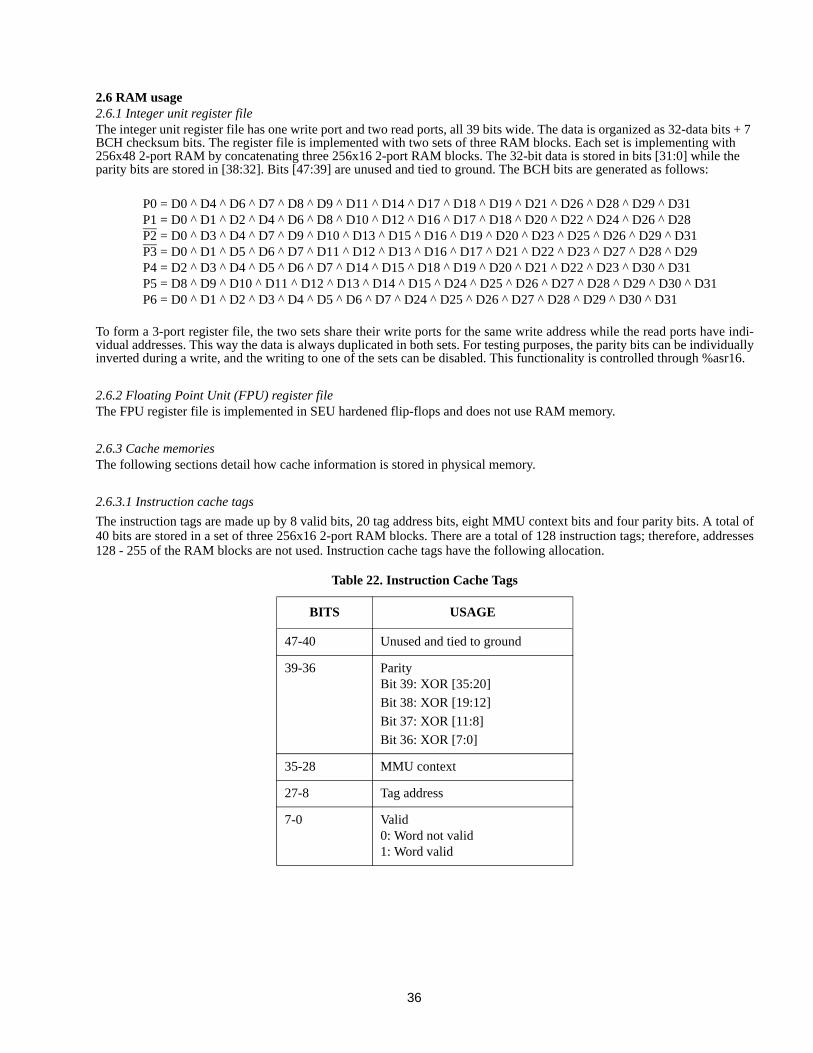
2.6.3.1 Instruction cache tags
The instruction tags are made up by 8 valid bits, 20 tag address bits, eight MMU context bits and four parity bits. A total of40 bits are stored in a set of three 256x16 2-port RAM blocks. There are a total of 128 instruction tags; therefore, addresses128 - 255 of the RAM blocks are not used. Instruction cache tags have the following allocation.
Table 22. Instruction Cache Tags
BITS USAGE
47-40 Unused and tied to ground
39-36 ParityBit 39: XOR [35:20]
Bit 38: XOR [19:12]
Bit 37: XOR [11:8]
Bit 36: XOR [7:0]
35-28 MMU context
27-8 Tag address
7-0 Valid0: Word not valid1: Word valid
37
2.6.3.2 Data cache tags
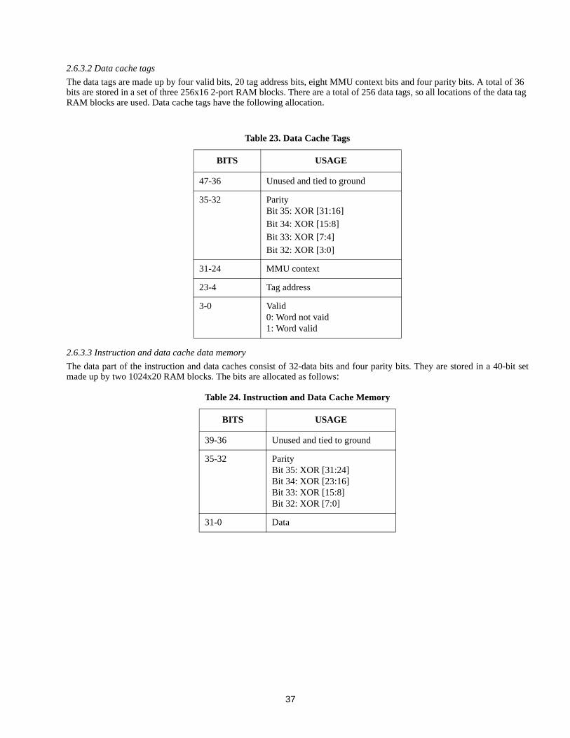
The data tags are made up by four valid bits, 20 tag address bits, eight MMU context bits and four parity bits. A total of 36 bits are stored in a set of three 256x16 2-port RAM blocks. There are a total of 256 data tags, so all locations of the data tag RAM blocks are used. Data cache tags have the following allocation.
2.6.3.3 Instruction and data cache data memory
The data part of the instruction and data caches consist of 32-data bits and four parity bits. They are stored in a 40-bit setmade up by two 1024x20 RAM blocks. The bits are allocated as follows:
Table 23. Data Cache Tags
BITS USAGE
47-36 Unused and tied to ground
35-32 ParityBit 35: XOR [31:16]
Bit 34: XOR [15:8]
Bit 33: XOR [7:4]
Bit 32: XOR [3:0]
31-24 MMU context
23-4 Tag address
3-0 Valid0: Word not vaid1: Word valid
Table 24. Instruction and Data Cache Memory
BITS USAGE
39-36 Unused and tied to ground
35-32 ParityBit 35: XOR [31:24]Bit 34: XOR [23:16]Bit 33: XOR [15:8]Bit 32: XOR [7:0]
31-0 Data
38
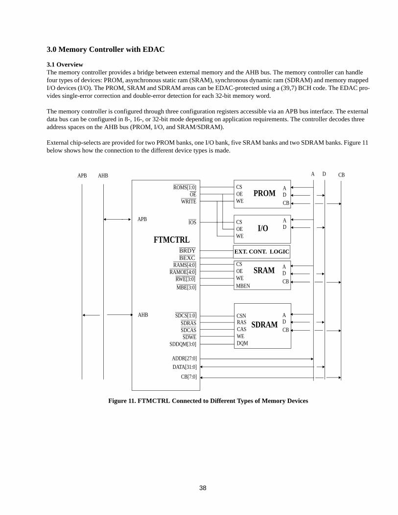
3.0 Memory Controller with EDAC
3.1 OverviewThe memory controller provides a bridge between external memory and the AHB bus. The memory controller can handle four types of devices: PROM, asynchronous static ram (SRAM), synchronous dynamic ram (SDRAM) and memory mapped I/O devices (I/O). The PROM, SRAM and SDRAM areas can be EDAC-protected using a (39,7) BCH code. The EDAC pro-vides single-error correction and double-error detection for each 32-bit memory word.
The memory controller is configured through three configuration registers accessible via an APB bus interface. The external data bus can be configured in 8-, 16-, or 32-bit mode depending on application requirements. The controller decodes three address spaces on the AHB bus (PROM, I/O, and SRAM/SDRAM).
External chip-selects are provided for two PROM banks, one I/O bank, five SRAM banks and two SDRAM banks. Figure 11 below shows how the connection to the different device types is made.
Figure 11. FTMCTRL Connected to Different Types of Memory Devices
CSOEWE
ADPROM
CSOEWE
I/O
CSOEWE
SRAMRAMS[4:0]
RAMOE[4:0]RWE[3:0]
ROMS[1:0]OE
WRITE
IOS
A D
FTMCTRL
ADDR[27:0]
DATA[31:0]
RASCASWE
SDRAMSDRASSDCASSDWE
DQMSDDQM[3:0]
CSNSDCS[1:0]
AHBAPB
MBENMBE[3:0]
APB
AHB
CB
CB
AD
AD
CB
AD
CB
CB[7:0]
BRDYBEXC
EXT. CONT. LOGIC
39
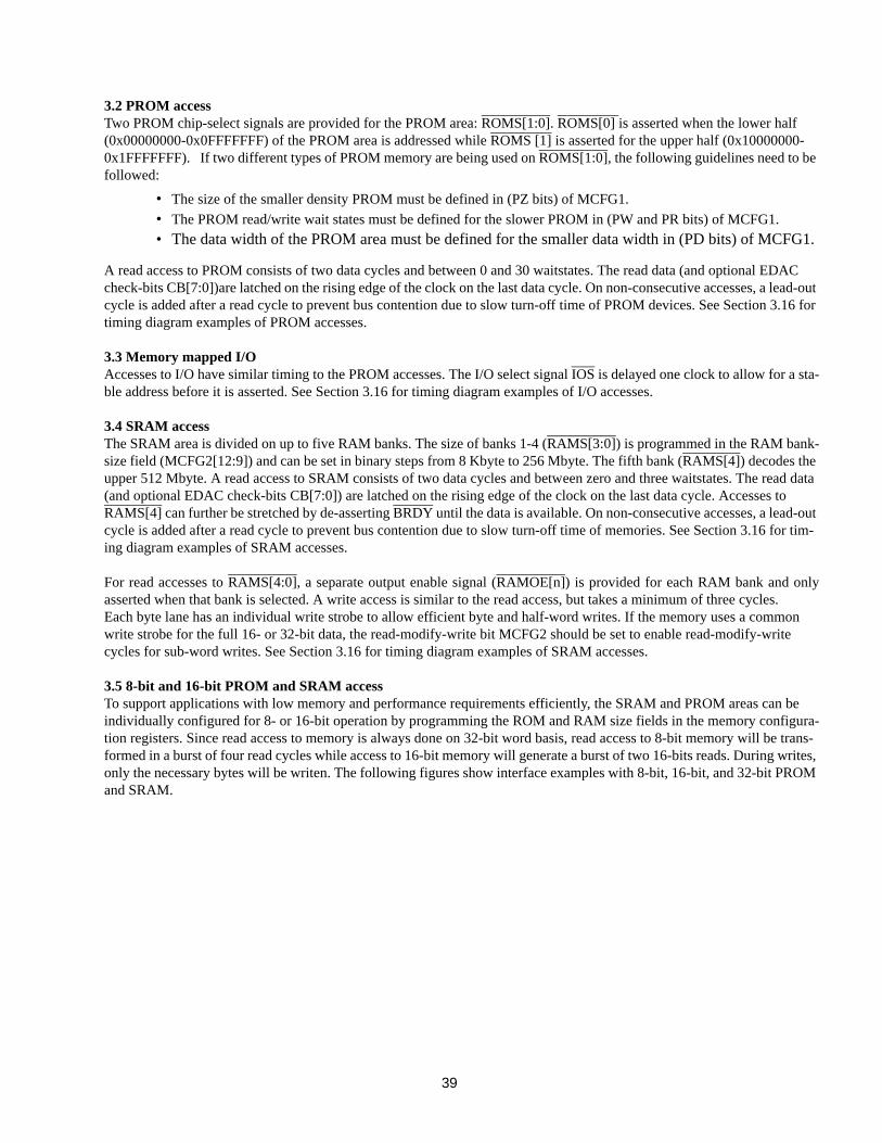
3.2 PROM accessTwo PROM chip-select signals are provided for the PROM area: ROMS[1:0]. ROMS[0] is asserted when the lower half (0x00000000-0x0FFFFFFF) of the PROM area is addressed while ROMS [1] is asserted for the upper half (0x10000000-0x1FFFFFFF). If two different types of PROM memory are being used on ROMS[1:0], the following guidelines need to be followed:
• The size of the smaller density PROM must be defined in (PZ bits) of MCFG1.
• The PROM read/write wait states must be defined for the slower PROM in (PW and PR bits) of MCFG1.
• The data width of the PROM area must be defined for the smaller data width in (PD bits) of MCFG1.
A read access to PROM consists of two data cycles and between 0 and 30 waitstates. The read data (and optional EDAC check-bits CB[7:0])are latched on the rising edge of the clock on the last data cycle. On non-consecutive accesses, a lead-out cycle is added after a read cycle to prevent bus contention due to slow turn-off time of PROM devices. See Section 3.16 for timing diagram examples of PROM accesses.
3.3 Memory mapped I/OAccesses to I/O have similar timing to the PROM accesses. The I/O select signal IOS is delayed one clock to allow for a sta-ble address before it is asserted. See Section 3.16 for timing diagram examples of I/O accesses.
3.4 SRAM accessThe SRAM area is divided on up to five RAM banks. The size of banks 1-4 (RAMS[3:0]) is programmed in the RAM bank-size field (MCFG2[12:9]) and can be set in binary steps from 8 Kbyte to 256 Mbyte. The fifth bank (RAMS[4]) decodes the upper 512 Mbyte. A read access to SRAM consists of two data cycles and between zero and three waitstates. The read data (and optional EDAC check-bits CB[7:0]) are latched on the rising edge of the clock on the last data cycle. Accesses to RAMS[4] can further be stretched by de-asserting BRDY until the data is available. On non-consecutive accesses, a lead-out cycle is added after a read cycle to prevent bus contention due to slow turn-off time of memories. See Section 3.16 for tim-ing diagram examples of SRAM accesses.
For read accesses to RAMS[4:0], a separate output enable signal (RAMOE[n]) is provided for each RAM bank and onlyasserted when that bank is selected. A write access is similar to the read access, but takes a minimum of three cycles.Each byte lane has an individual write strobe to allow efficient byte and half-word writes. If the memory uses a common write strobe for the full 16- or 32-bit data, the read-modify-write bit MCFG2 should be set to enable read-modify-write cycles for sub-word writes. See Section 3.16 for timing diagram examples of SRAM accesses.
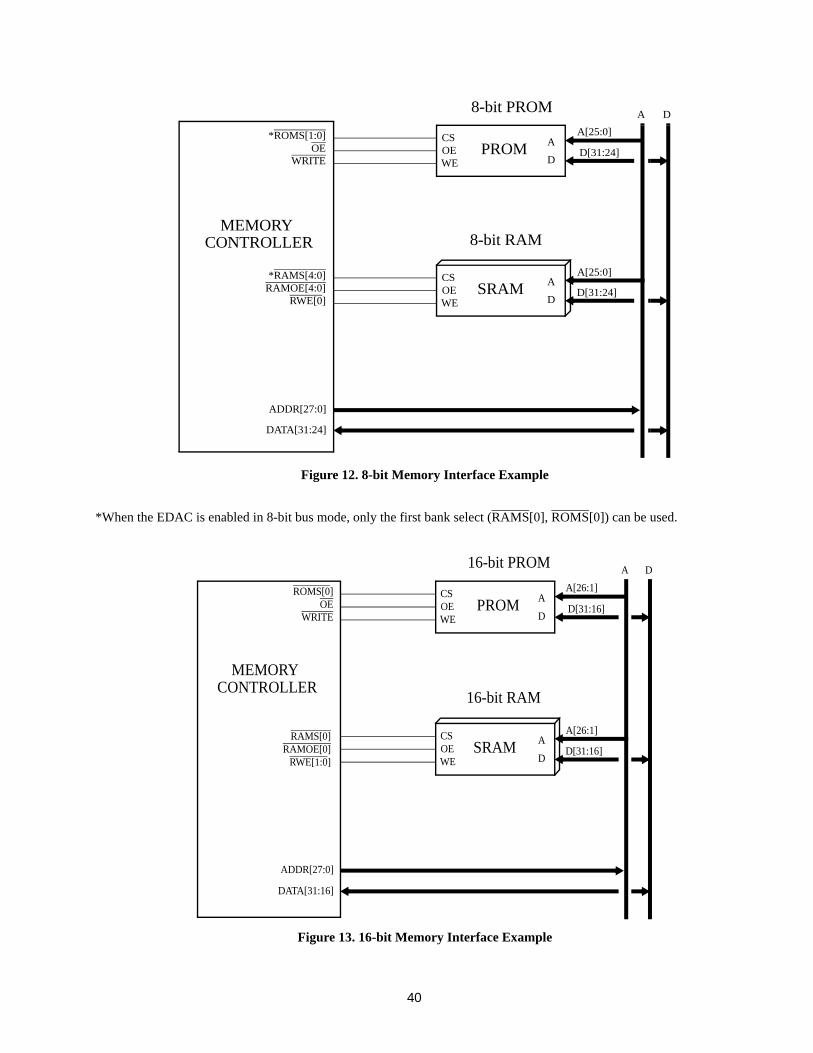
3.5 8-bit and 16-bit PROM and SRAM accessTo support applications with low memory and performance requirements efficiently, the SRAM and PROM areas can be individually configured for 8- or 16-bit operation by programming the ROM and RAM size fields in the memory configura-tion registers. Since read access to memory is always done on 32-bit word basis, read access to 8-bit memory will be trans-formed in a burst of four read cycles while access to 16-bit memory will generate a burst of two 16-bits reads. During writes, only the necessary bytes will be writen. The following figures show interface examples with 8-bit, 16-bit, and 32-bit PROM and SRAM.
40
*When the EDAC is enabled in 8-bit bus mode, only the first bank select (RAMS[0], ROMS[0]) can be used.
Figure 12. 8-bit Memory Interface Example
CSOEWE
A
DPROM
CSOEWE
A
DSRAM
*RAMS[4:0]RAMOE[4:0]
RWE[0]
*ROMS[1:0]OE
A D
MEMORY
ADDR[27:0]
DATA[31:24]
D[31:24]
D[31:24]
A[25:0]
A[25:0]
WRITE
8-bit PROM
8-bit RAMCONTROLLER
Figure 13. 16-bit Memory Interface Example
CSOEWE
A
DPROM
CSOEWE
A
DSRAM
RAMS[0]RAMOE[0]
RWE[1:0]
ROMS[0]OE
A D
ADDR[27:0]
DATA[31:16]
D[31:16]
D[31:16]
A[26:1]
A[26:1]
WRITE
16-bit PROM
16-bit RAM
MEMORYCONTROLLER
41
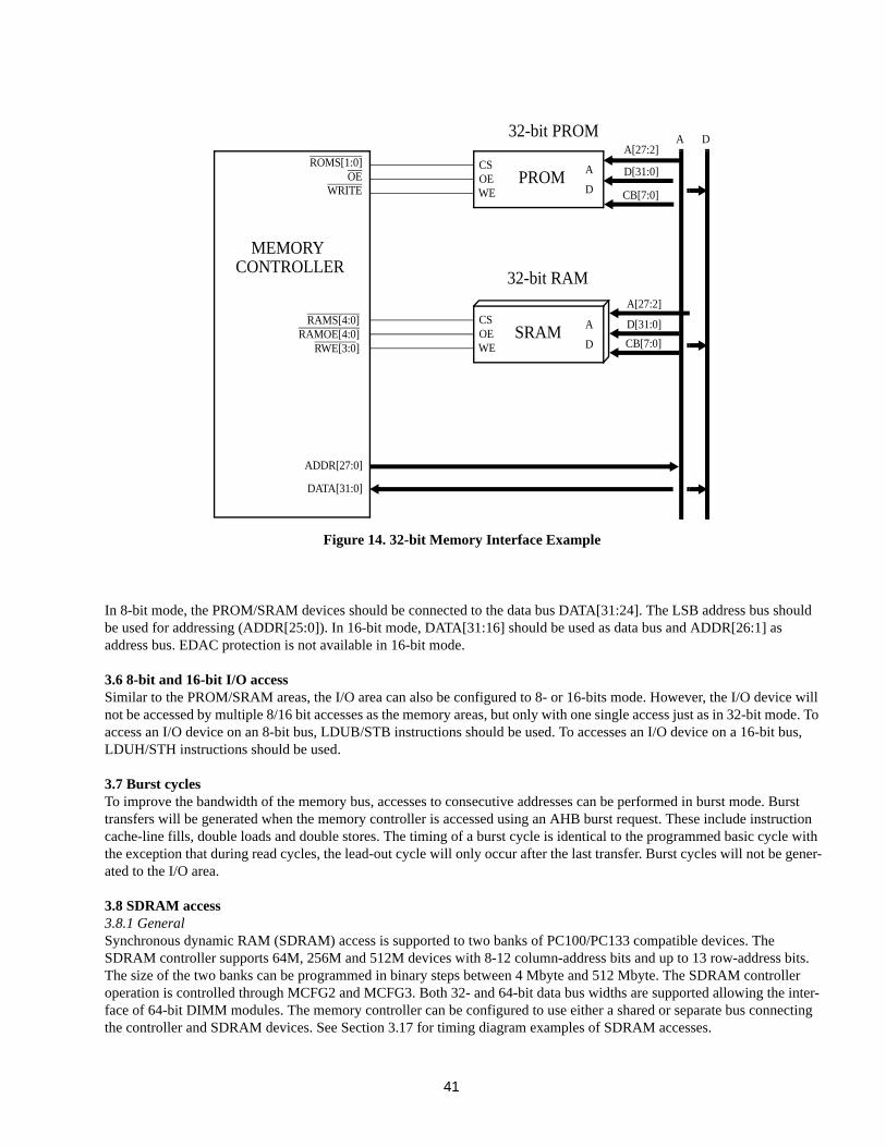
In 8-bit mode, the PROM/SRAM devices should be connected to the data bus DATA[31:24]. The LSB address bus should be used for addressing (ADDR[25:0]). In 16-bit mode, DATA[31:16] should be used as data bus and ADDR[26:1] as address bus. EDAC protection is not available in 16-bit mode.
3.6 8-bit and 16-bit I/O accessSimilar to the PROM/SRAM areas, the I/O area can also be configured to 8- or 16-bits mode. However, the I/O device will not be accessed by multiple 8/16 bit accesses as the memory areas, but only with one single access just as in 32-bit mode. To access an I/O device on an 8-bit bus, LDUB/STB instructions should be used. To accesses an I/O device on a 16-bit bus, LDUH/STH instructions should be used.
3.7 Burst cyclesTo improve the bandwidth of the memory bus, accesses to consecutive addresses can be performed in burst mode. Burst transfers will be generated when the memory controller is accessed using an AHB burst request. These include instruction cache-line fills, double loads and double stores. The timing of a burst cycle is identical to the programmed basic cycle with the exception that during read cycles, the lead-out cycle will only occur after the last transfer. Burst cycles will not be gener-ated to the I/O area.
3.8 SDRAM access3.8.1 GeneralSynchronous dynamic RAM (SDRAM) access is supported to two banks of PC100/PC133 compatible devices. The SDRAM controller supports 64M, 256M and 512M devices with 8-12 column-address bits and up to 13 row-address bits. The size of the two banks can be programmed in binary steps between 4 Mbyte and 512 Mbyte. The SDRAM controller operation is controlled through MCFG2 and MCFG3. Both 32- and 64-bit data bus widths are supported allowing the inter-face of 64-bit DIMM modules. The memory controller can be configured to use either a shared or separate bus connecting the controller and SDRAM devices. See Section 3.17 for timing diagram examples of SDRAM accesses.
CSOEWE
A
DPROM
CSOEWE
A
DSRAM
RAMS[4:0]RAMOE[4:0]
RWE[3:0]
ROMS[1:0]OE
A D
ADDR[27:0]
DATA[31:0]
D[31:0]
D[31:0]
A[27:2]
A[27:2]
WRITE
32-bit PROM
32-bit RAM
MEMORYCONTROLLER
CB[7:0]
CB[7:0]
Figure 14. 32-bit Memory Interface Example
42
3.8.2 Address mappingTwo SDRAM chip-select signals are used for address decoding. SDRAM area is mapped into the upper half of the RAM area. When the SDRAM enable bit is set in MCFG2, the controller is enabled and mapped into upper half of the RAM area, as long as the SRAM disable bit is not set. If the SRAM disable bit is set, all access to SRAM is disabled and the SDRAM banks are mapped into the lower half of the RAM area.
3.8.3 InitializationWhen the SDRAM controller is enabled, it automatically performs the SDRAM initialization sequence of one PRE-CHARGE command, eight AUTO-REFRESH command and LOAD-MODE-REG command on both banks simultaneously. The controller programs the SDRAM to use page burst on read and single location access on write.
3.8.4 Configurable SDRAM timing parametersTo provide optimum access cycles for different SDRAM devices (and at different frequencies), three SDRAM parameters can be programmed via MCGF2: TCAS, TRP and TRFCD. The value of these field affects the SDRAM timing as described in Table 25.
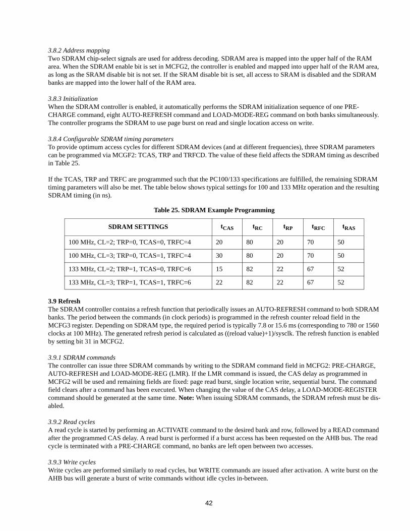
If the TCAS, TRP and TRFC are programmed such that the PC100/133 specifications are fulfilled, the remaining SDRAM timing parameters will also be met. The table below shows typical settings for 100 and 133 MHz operation and the resulting SDRAM timing (in ns).
3.9 RefreshThe SDRAM controller contains a refresh function that periodically issues an AUTO-REFRESH command to both SDRAM banks. The period between the commands (in clock periods) is programmed in the refresh counter reload field in the MCFG3 register. Depending on SDRAM type, the required period is typically 7.8 or 15.6 ms (corresponding to 780 or 1560 clocks at 100 MHz). The generated refresh period is calculated as ((reload value)+1)/sysclk. The refresh function is enabled by setting bit 31 in MCFG2.
3.9.1 SDRAM commandsThe controller can issue three SDRAM commands by writing to the SDRAM command field in MCFG2: PRE-CHARGE, AUTO-REFRESH and LOAD-MODE-REG (LMR). If the LMR command is issued, the CAS delay as programmed in MCFG2 will be used and remaining fields are fixed: page read burst, single location write, sequential burst. The command field clears after a command has been executed. When changing the value of the CAS delay, a LOAD-MODE-REGISTER command should be generated at the same time. Note: When issuing SDRAM commands, the SDRAM refresh must be dis-abled.
3.9.2 Read cyclesA read cycle is started by performing an ACTIVATE command to the desired bank and row, followed by a READ command after the programmed CAS delay. A read burst is performed if a burst access has been requested on the AHB bus. The read cycle is terminated with a PRE-CHARGE command, no banks are left open between two accesses.
3.9.3 Write cyclesWrite cycles are performed similarly to read cycles, but WRITE commands are issued after activation. A write burst on the AHB bus will generate a burst of write commands without idle cycles in-between.
Table 25. SDRAM Example Programming
SDRAM SETTINGS tCAS tRC tRP tRFC tRAS
100 MHz, CL=2; TRP=0, TCAS=0, TRFC=4 20 80 20 70 50
100 MHz, CL=3; TRP=0, TCAS=1, TRFC=4 30 80 20 70 50
133 MHz, CL=2; TRP=1, TCAS=0, TRFC=6 15 82 22 67 52
133 MHz, CL=3; TRP=1, TCAS=1, TRFC=6 22 82 22 67 52
43
3.9.4 Address busThe memory controller uses a common address bus for PROM, I/O SRAM and SDRAM. SDRAM connected to the address bus should use ADDR[14:2] for the row select and ADDR[16:15] for the bank select.
3.9.5 Data busThe memory controller uses a common data bus for PROM, I/O, SRAM and SDRAM. The SDRAM always uses a 32-bit data bus. The SDRAM can access a 64-bit SDRAM bus at half the data capacity.
3.9.6 ClockingThe SDRAM memory is clocked by the SDCLK output. This output is a buffered copy of the internal system clock. The SDCLK output will be available as long as the system clock (SYSCLK) is operating.
3.9.7 InitializationEach time the SDRAM is enabled (by setting bit 14 in MCFG2), an SDRAM initialization sequence will be sent to both SDRAM banks. The sequence consists of one PRECHARGE command, eight AUTO-REFRESH command and one LOAD-COMMAND-REGISTER command.
3.10 Memory EDACThe FTMCTRL is provided with an error detected and correction (EDAC) controller that can correct one error and detect two errors in a 32-bit word. For each word, a 7-bit checksum is generated according to the equations below. A correctable error will be handled transparently by the memory controller, but will add one waitstate to the access. If an un-correctable error (double-error) is detected, the current AHB cycle will end with an error response. The EDAC can be used during access to PROM, SRAM and SDRAM areas by setting the corresponding EDAC enable bits in the MCFG3 register. The equations below show how the EDAC checkbits are generated:
CB0 = D0 ^ D4 ^ D6 ^ D7 ^ D8 ^ D9 ^ D11 ^ D14 ^ D17 ^ D18 ^ D19 ^ D21 ^ D26 ^ D28 ^ D29 ^ D31CB1 = D0 ^ D1 ^ D2 ^ D4 ^ D6 ^ D8 ^ D10 ^ D12 ^ D16 ^ D17 ^ D18 ^ D20 ^ D22 ^ D24 ^ D26 ^ D28CB2 = D0 ^ D3 ^ D4 ^ D7 ^ D9 ^ D10 ^ D13 ^ D15 ^ D16 ^ D19 ^ D20 ^ D23 ^ D25 ^ D26 ^ D29 ^ D31CB3 = D0 ^ D1 ^ D5 ^ D6 ^ D7 ^ D11 ^ D12 ^ D13 ^ D16 ^ D17 ^ D21 ^ D22 ^ D23 ^ D27 ^ D28 ^ D29CB4 = D2 ^ D3 ^ D4 ^ D5 ^ D6 ^ D7 ^ D14 ^ D15 ^ D18 ^ D19 ^ D20 ^ D21 ^ D22 ^ D23 ^ D30 ^ D31CB5 = D8 ^ D9 ^ D10 ^ D11 ^ D12 ^ D13 ^ D14 ^ D15 ^ D24 ^ D25 ^ D26 ^ D27 ^ D28 ^ D29 ^ D30 ^ D31CB6 = D0 ^ D1 ^ D2 ^ D3 ^ D4 ^ D5 ^ D6 ^ D7 ^ D24 ^ D25 ^ D26 ^ D27 ^ D28 ^ D29 ^ D30 ^ D31
If the memory is configured in 8-bit mode, the EDAC checkbit bus (CB[7:0]) is not used, but it is still possible to use EDAC protection. This is done by allocating the top 20% of the memory bank to the EDAC checksums. If the EDAC is enabled, a read access reads the data bytes from the logical address and the EDAC checksum from the top part of the memory bank. A write cycle is performed the same way. In this way, 80% of the bank memory is available as program or data memory while the top 20% is used for check bits. The size of the memory bank is determined from the settings in MCFG1 and MCFG2. The EDAC cannot be used on memory areas configured in 16-bit mode.
NOTE: When the EDAC is enabled in 8-bit bus mode, only the first bank select (ROMS[0], RAMS[0]) can be used.
The operation of the EDAC can be tested trough the MCFG3 register. If the WB (write bypass) bit is set, the value in the TCB field replaces the normal checkbits during memory write cycles. If the RB (read bypass) is set, the memory checkbits of the loaded data will be stored in the TCB field during memory read cycles. Note: when the EDAC is enabled, the RMW bit in memory configuration register 2 must be set.
44
3.11 Using BRDYThe BRDY signal can be used to stretch access cycles to the PROM and I/O areas and the SRAM area decoded by RAMS[4]. The accesses will always have at least the pre-programmed number of waitstates as defined in registers MCFG1 and MCFG2, but will be further stretched until BRDY is asserted. BRDY should be asserted in the cycle preceding the last one. If bit 29 in MCFG1 is set, BRDY can be asserted asynchronously with the system clock. In this case, the read data must be kept stable until the de-assertion of OE/RAMOE. The use of BRDY can be enabled separately for the PROM, I/O and RAMS[4] areas. See Section 3.16 for timing diagram examples with BRDY.
3.12 Access errorsAn access error can be signalled by asserting the BEXC signal which is sampled together with the data. If the usage of BEXC is enabled in register MCFG1, an error response will be generated on the internal AHB bus. BEXC can be enabled or disabled through register MCFG1 and is active for all areas (PROM, I/O an RAM). See Section 3.16 for timing diagram examples using BEXC.
3.13 Attaching an external DRAM controllerTo attach an external DRAM controller, RAMS[4] should be used since it allows the cycle time to vary through the use of BRDY. In this way, delays can be inserted as required for opening of banks and refresh.
3.14 RegistersThe core is programmed through registers mapped into APB address space.
Table 26. FTMCTRL Memory Controller Registers
REGISTER APB ADDRESS
Memory configuration register 1 (MCFG1) 0x80000000
Memory configuration register 2 (MCFG2) 0x80000004
Memory configuration register 3 (MCFG3) 0x80000008
45
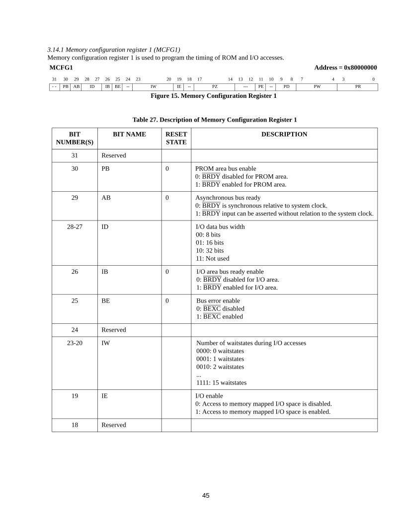
3.14.1 Memory configuration register 1 (MCFG1)Memory configuration register 1 is used to program the timing of ROM and I/O accesses.
Table 27. Description of Memory Configuration Register 1
BIT NUMBER(S)
BIT NAME RESET STATE
DESCRIPTION
31 Reserved
30 PB 0 PROM area bus enable0: BRDY disabled for PROM area.1: BRDY enabled for PROM area.
29 AB 0 Asynchronous bus ready0: BRDY is synchronous relative to system clock.1: BRDY input can be asserted without relation to the system clock.
28-27 ID I/O data bus width00: 8 bits01: 16 bits10: 32 bits11: Not used
26 IB 0 I/O area bus ready enable0: BRDY disabled for I/O area.1: BRDY enabled for I/O area.
25 BE 0 Bus error enable0: BEXC disabled1: BEXC enabled
24 Reserved
23-20 IW Number of waitstates during I/O accesses0000: 0 waitstates0001: 1 waitstates0010: 2 waitstates...1111: 15 waitstates
19 IE I/O enable0: Access to memory mapped I/O space is disabled.1: Access to memory mapped I/O space is enabled.
18 Reserved
MCFG1 Address = 0x80000000
31 30 29 28 27 26 25 24 23 20 19 18 17 14 13 12 11 10 9 8 7 4 3 0
- - PB AB ID IB BE -- IW IE -- PZ --- PE -- PD PW PR
Figure 15. Memory Configuration Register 1
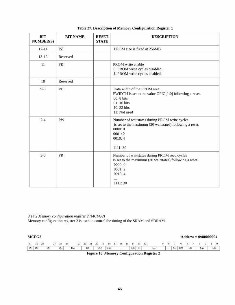
46
3.14.2 Memory configuration register 2 (MCFG2) Memory configuration register 2 is used to control the timing of the SRAM and SDRAM.
BIT NUMBER(S)
BIT NAME RESET STATE
DESCRIPTION
17-14 PZ PROM size is fixed at 256MB
13-12 Reserved
11 PE PROM write enable0: PROM write cycles disabled.1: PROM write cycles enabled.
10 Reserved
9-8 PD Data width of the PROM areaPWIDTH is set to the value GPIO[1:0] following a reset.00: 8 bits01: 16 bits10: 32 bits11: Not used
7-4 PW Number of waitstates during PROM write cycles is set to the maximum (30 waitstates) following a reset.0000: 00001: 20010: 4...1111: 30
3-0 PR Number of waitstates during PROM read cyclesis set to the maximum (30 waitstates) following a reset.0000: 00001: 20010: 4...1111: 30
Table 27. Description of Memory Configuration Register 1
MCFG2 Address = 0x80000004
31 30 29 27 26 25 23 22 21 20 19 18 17 16 15 14 13 12 9 8 7 6 5 4 3 2 1 0
DR DP DF DC DZ DS DD BW -- DE SI SZ -- SB RM SD SW SR
Figure 16. Memory Configuration Register 2
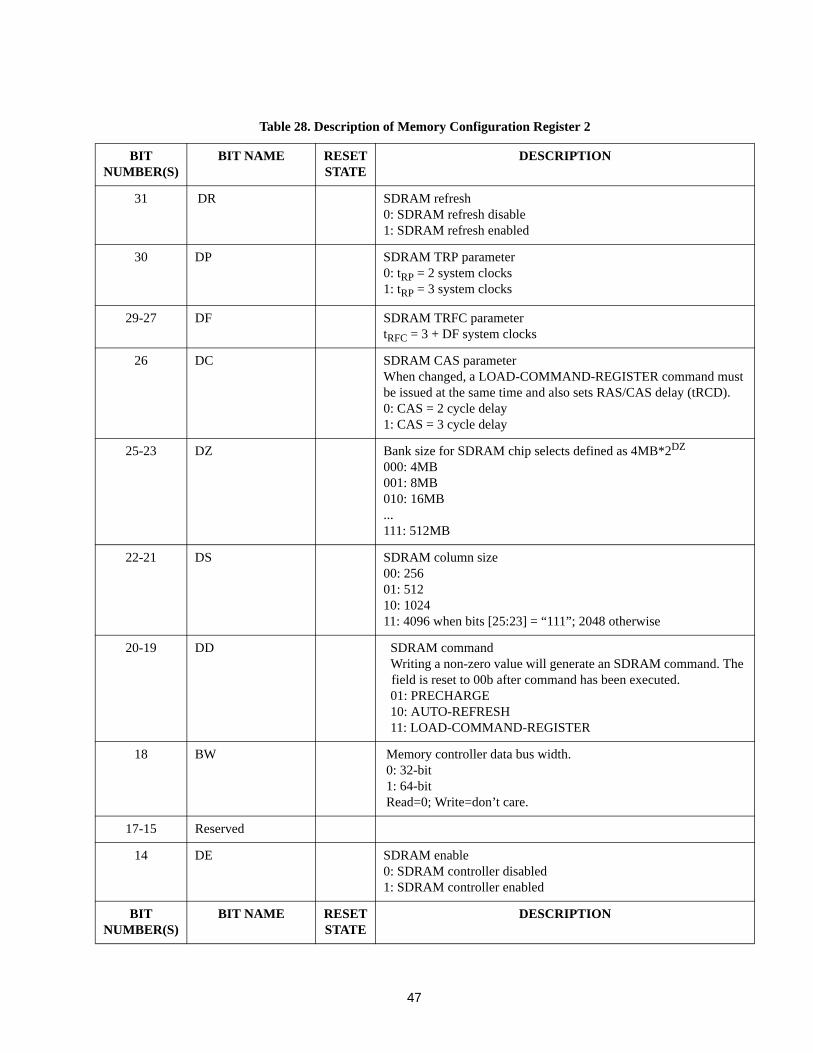
47
Table 28. Description of Memory Configuration Register 2
BIT NUMBER(S)
BIT NAME RESET STATE
DESCRIPTION
31 DR SDRAM refresh0: SDRAM refresh disable1: SDRAM refresh enabled
30 DP SDRAM TRP parameter0: tRP = 2 system clocks1: tRP = 3 system clocks
29-27 DF SDRAM TRFC parametertRFC = 3 + DF system clocks
26 DC SDRAM CAS parameterWhen changed, a LOAD-COMMAND-REGISTER command must be issued at the same time and also sets RAS/CAS delay (tRCD).0: CAS = 2 cycle delay1: CAS = 3 cycle delay
25-23 DZ Bank size for SDRAM chip selects defined as 4MB*2DZ
000: 4MB001: 8MB010: 16MB...111: 512MB
22-21 DS SDRAM column size 00: 25601: 51210: 102411: 4096 when bits [25:23] = “111”; 2048 otherwise
20-19 DD SDRAM commandWriting a non-zero value will generate an SDRAM command. The field is reset to 00b after command has been executed.01: PRECHARGE10: AUTO-REFRESH11: LOAD-COMMAND-REGISTER
18 BW Memory controller data bus width.0: 32-bit1: 64-bitRead=0; Write=don’t care.
17-15 Reserved
14 DE SDRAM enable0: SDRAM controller disabled1: SDRAM controller enabled
BIT NUMBER(S)
BIT NAME RESET STATE
DESCRIPTION
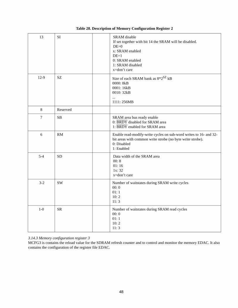
48
3.14.3 Memory configuration register 3 MCFG3 is contains the reload value for the SDRAM refresh counter and to control and monitor the memory EDAC. It also contains the configuration of the register file EDAC.
13 SI SRAM disableIf set together with bit 14 the SRAM will be disabled.DE=0x: SRAM enabledDE=10: SRAM enabled1: SRAM disabledx=don’t care
12-9 SZ Size of each SRAM bank as 8*2SZ kB0000: 8kB0001: 16kB0010: 32kB...1111: 256MB
8 Reserved
7 SB SRAM area bus ready enable0: BRDY disabled for SRAM area1: BRDY enabled for SRAM area
6 RM Enable read-modify-write cycles on sub-word writes to 16- and 32-bit areas with common write strobe (no byte write strobe).0: Disabled1: Enabled
5-4 SD Data width of the SRAM area00: 801: 161x: 32x=don’t care
3-2 SW Number of waitstates during SRAM write cycles00: 001: 110: 211: 3
1-0 SR Number of waitstates during SRAM read cycles00: 001: 110: 211: 3
Table 28. Description of Memory Configuration Register 2
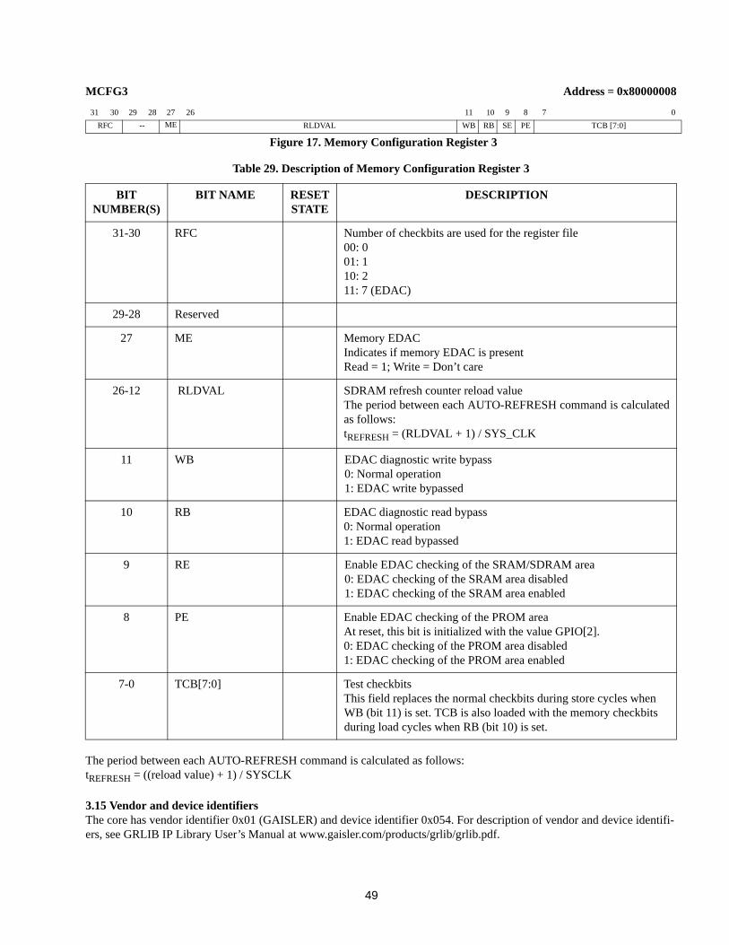
49
MCFG3 Address = 0x80000008
The period between each AUTO-REFRESH command is calculated as follows:tREFRESH = ((reload value) + 1) / SYSCLK
3.15 Vendor and device identifiersThe core has vendor identifier 0x01 (GAISLER) and device identifier 0x054. For description of vendor and device identifi-ers, see GRLIB IP Library User’s Manual at www.gaisler.com/products/grlib/grlib.pdf.
31 30 29 28 27 26 11 10 9 8 7 0
RFC -- ME RLDVAL WB RB SE PE TCB [7:0]
Figure 17. Memory Configuration Register 3
Table 29. Description of Memory Configuration Register 3
BIT NUMBER(S)
BIT NAME RESET STATE
DESCRIPTION
31-30 RFC Number of checkbits are used for the register file00: 001: 110: 211: 7 (EDAC)
29-28 Reserved
27 ME Memory EDACIndicates if memory EDAC is presentRead = 1; Write = Don’t care
26-12 RLDVAL SDRAM refresh counter reload valueThe period between each AUTO-REFRESH command is calculatedas follows:tREFRESH = (RLDVAL + 1) / SYS_CLK
11 WB EDAC diagnostic write bypass0: Normal operation1: EDAC write bypassed
10 RB EDAC diagnostic read bypass0: Normal operation1: EDAC read bypassed
9 RE Enable EDAC checking of the SRAM/SDRAM area0: EDAC checking of the SRAM area disabled1: EDAC checking of the SRAM area enabled
8 PE Enable EDAC checking of the PROM areaAt reset, this bit is initialized with the value GPIO[2].0: EDAC checking of the PROM area disabled1: EDAC checking of the PROM area enabled
7-0 TCB[7:0] Test checkbitsThis field replaces the normal checkbits during store cycles when WB (bit 11) is set. TCB is also loaded with the memory checkbits during load cycles when RB (bit 10) is set.
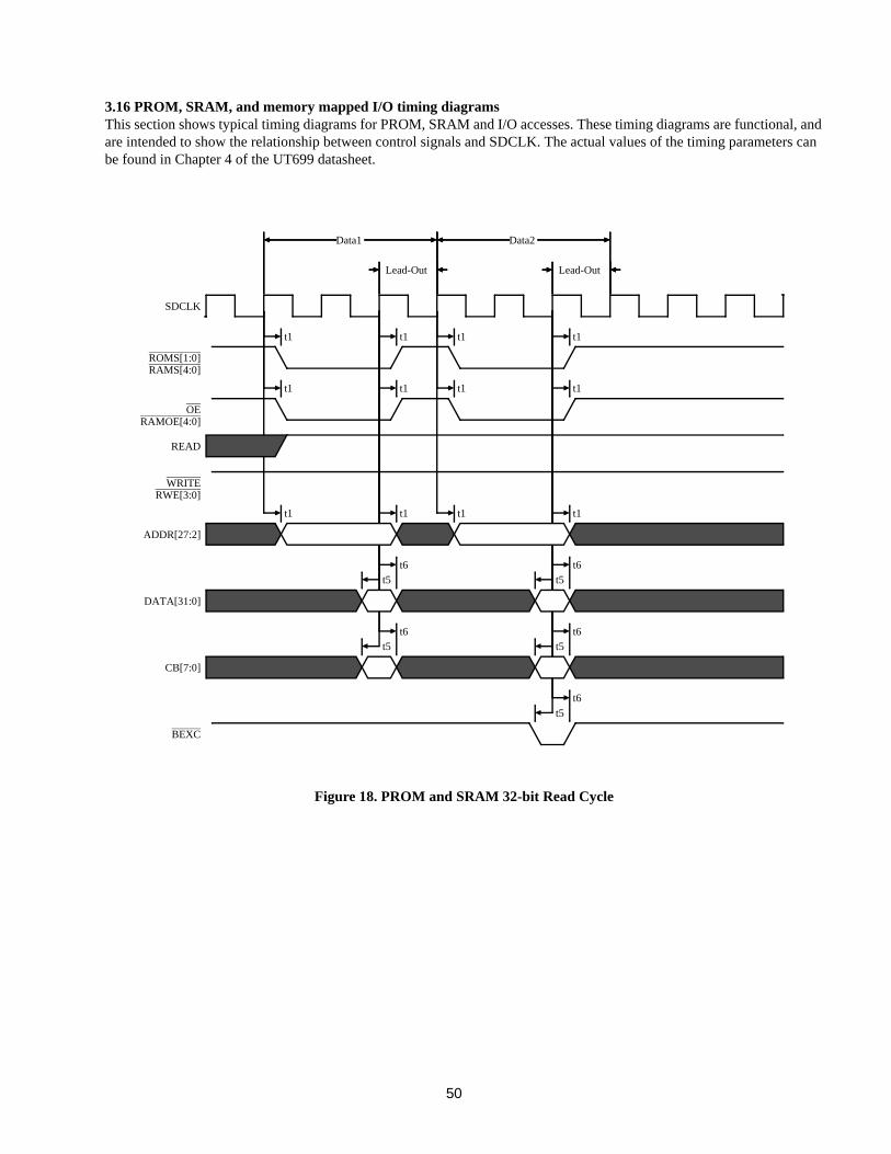
50
3.16 PROM, SRAM, and memory mapped I/O timing diagramsThis section shows typical timing diagrams for PROM, SRAM and I/O accesses. These timing diagrams are functional, and are intended to show the relationship between control signals and SDCLK. The actual values of the timing parameters can be found in Chapter 4 of the UT699 datasheet.
t6
t5
t6t5
t6t5
t6t5
t6t5
t1t1t1t1
t1t1t1t1
t1t1t1t1
Lead-Out
Data2
Lead-Out
Data1
SDCLK
ROMS[1:0]
OE
READ
WRITE
ADDR[27:2]
DATA[31:0]
CB[7:0]
BEXC
RAMS[4:0]
RAMOE[4:0]
RWE[3:0]
Figure 18. PROM and SRAM 32-bit Read Cycle
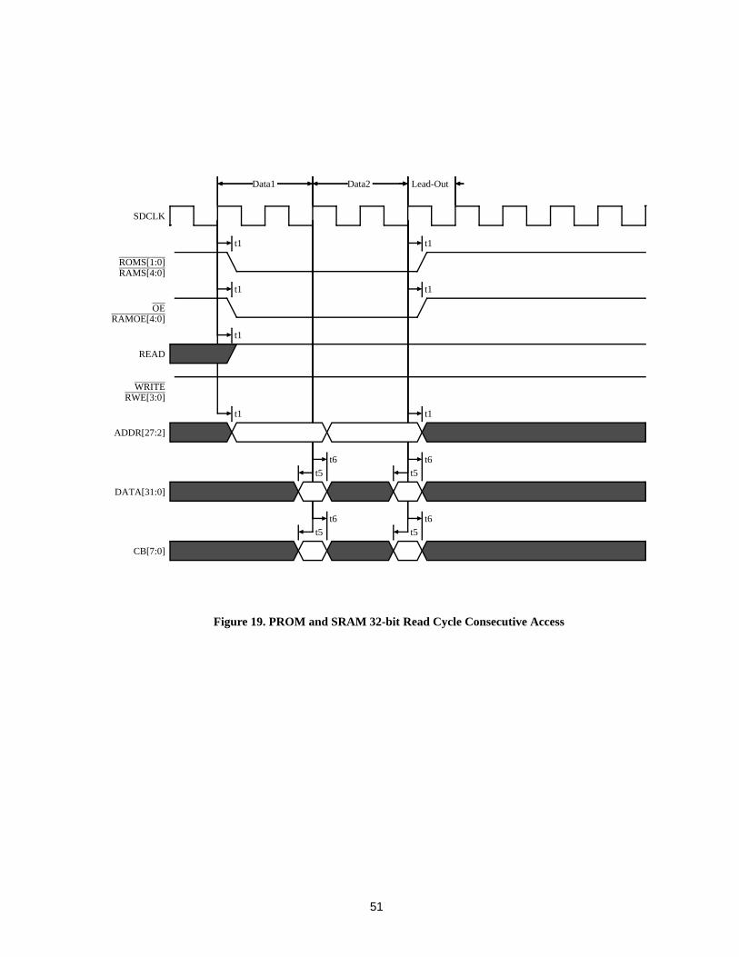
51
t6
t5
t6
t5
t6
t5
t6
t5
t1t1
t1
t1t1
t1t1
Lead-OutData2Data1
SDCLK
ROMS[1:0]
OE
READ
WRITE
ADDR[27:2]
DATA[31:0]
CB[7:0]
RAMS[4:0]
RAMOE[4:0]
RWE[3:0]
Figure 19. PROM and SRAM 32-bit Read Cycle Consecutive Access
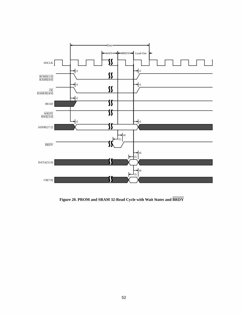
52
t6t5
t6
t5
t6
t5
t1t1
t1
t1t1
t1t1
BRDY Lead-OutnWS
Data
SDCLK
ROMS[1:0]
OE
READ
WRITE
ADDR[27:2]
BRDY
DATA[31:0]
CB[7:0]
RAMS[4:0]
RAMOE[4:0]
RWE[3:0]
Figure 20. PROM and SRAM 32-Read Cycle with Wait States and BRDY
53
t6
t5
t6
t5
t7
t1t1
t1
t1t1
t1t1
BRDY Lead-OutnWS
Data
SDCLK
ROMS[1:0]
OE
READ
WRITE
ADDR[27:2]
BRDY
DATA[31:0]
CB[7:0]
RAMS[4:0]
RAMOE[4:0]
RWE[3:0]
Figure 21. PROM and SRAM 32-Read Cycle Wait States and Asynchronous BRDY
54
t6t5
t6t5
t6t5
t6t5
t1t1t1t1
t1t1t1t1
t1t1t1t1
Lead-Out
Data2
Lead-Out
Data1
SDCLK
ROMS[1:0]
OE
READ
WRITE
ADDR[27:1]
DATA[31:16]
CB[7:0]
RAMS[4:0]
RAMOE[4:0]
RWE[3:0]
Figure 22. PROM and SRAM 16-bit Read Cycle
55
t6t5
t6t5
t6t5
t6t5
t1t1t1t1t1t1t1t1
t1t1t1t1t1t1t1t1
t1t1t1t1t1t1t1t1
Lead-Out
Data4
Lead-Out
Data3
Lead-Out
Data2
Lead-Out
Data1
SDCLK
ROMS[1:0]
OE
READ
WRITE
ADDR[27:0]
DATA[31:24]
RAMS[4:0]
RAMOE[4:0]
RWE[3:0]
Figure 23. PROM and SRAM 8-bit Read Cycle on a 32-bit Bus
56
t3t2
t3t2
t1t1
t1t1
t1t1
t1t1
Lead-Out
Data
Lead-In
SDCLK
ROMS[1:0]
OE
READ
WRITE
ADDR[27:2]
DATA[31:0]
CB[7:0]
RAMS[4:0]
RAMOE[4:0]
RWE[3:0]
Figure 24. PROM and SRAM 32-bit Write Cycle on a 32-bit Bus
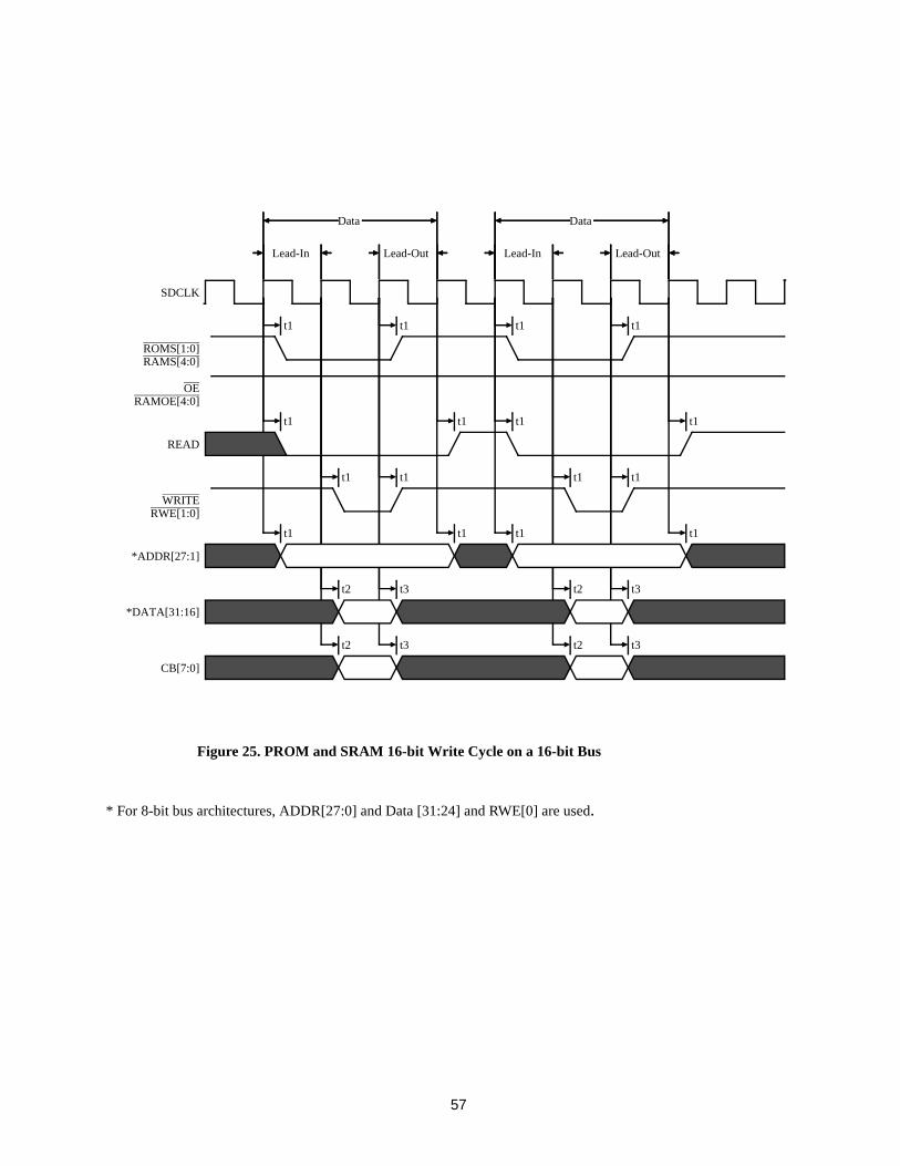
57
* For 8-bit bus architectures, ADDR[27:0] and Data [31:24] and RWE[0] are used.
t3t2t3t2
t3t2t3t2
t1t1t1t1
t1t1t1t1
t1t1t1t1
t1t1t1t1
Lead-Out
Data
Lead-InLead-Out
Data
Lead-In
SDCLK
ROMS[1:0]
OE
READ
WRITE
*ADDR[27:1]
*DATA[31:16]
CB[7:0]
RAMS[4:0]
RAMOE[4:0]
RWE[1:0]
Figure 25. PROM and SRAM 16-bit Write Cycle on a 16-bit Bus
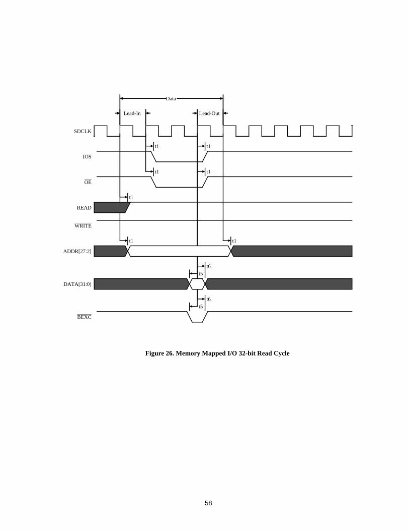
58
t6t5
t6
t5
t1t1
t1
t1t1
t1t1
Lead-OutLead-In
Data
SDCLK
IOS
OE
READ
WRITE
ADDR[27:2]
DATA[31:0]
BEXC
Figure 26. Memory Mapped I/O 32-bit Read Cycle
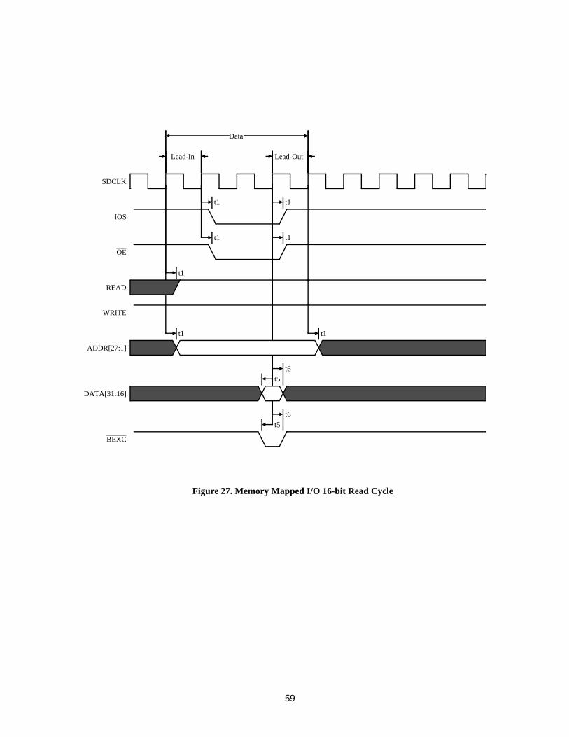
59
t6t5
t6
t5
t1t1
t1
t1t1
t1t1
Lead-OutLead-In
Data
SDCLK
IOS
OE
READ
WRITE
ADDR[27:1]
DATA[31:16]
BEXC
Figure 27. Memory Mapped I/O 16-bit Read Cycle
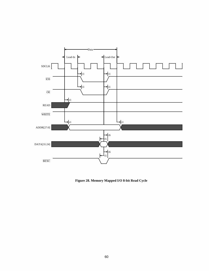
60
t6t5
t6
t5
t1t1
t1
t1t1
t1t1
Lead-OutLead-In
Data
SDCLK
IOS
OE
READ
WRITE
ADDR[27:0]
DATA[31:24]
BEXC
Figure 28. Memory Mapped I/O 8-bit Read Cycle
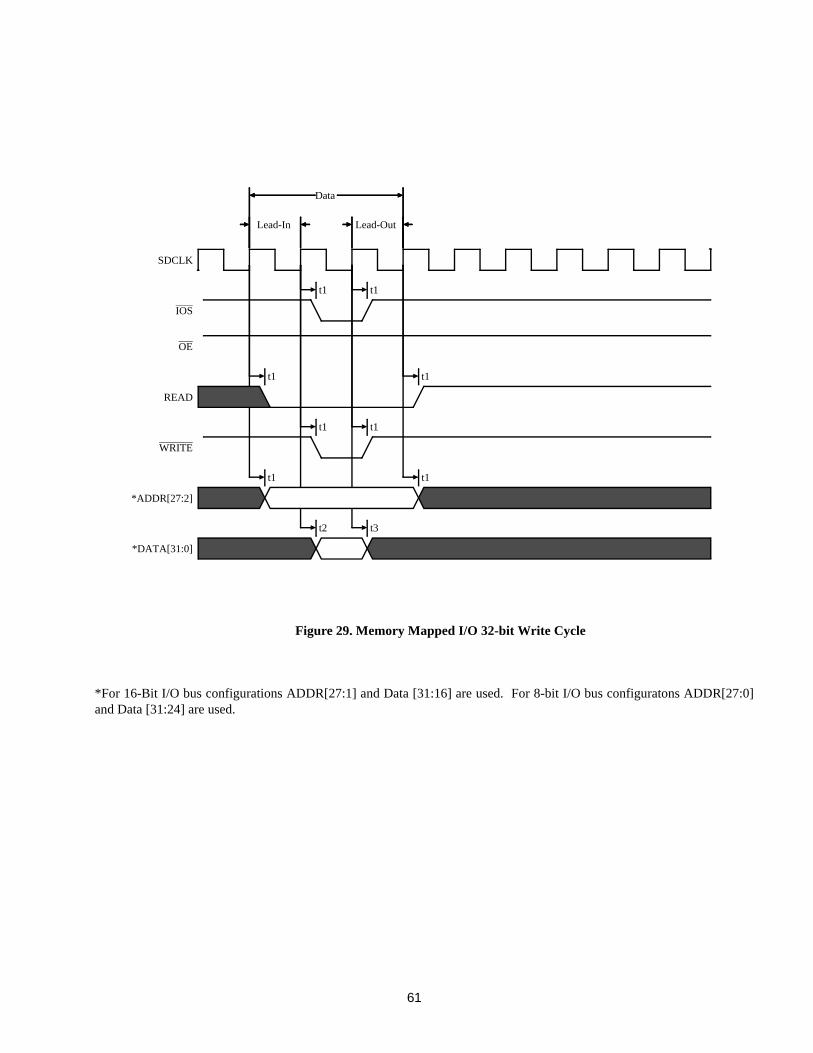
61
*For 16-Bit I/O bus configurations ADDR[27:1] and Data [31:16] are used. For 8-bit I/O bus configuratons ADDR[27:0]and Data [31:24] are used.
t3t2
t1t1
t1t1
t1t1
t1t1
Lead-Out
Data
Lead-In
SDCLK
IOS
OE
READ
WRITE
*ADDR[27:2]
*DATA[31:0]
Figure 29. Memory Mapped I/O 32-bit Write Cycle
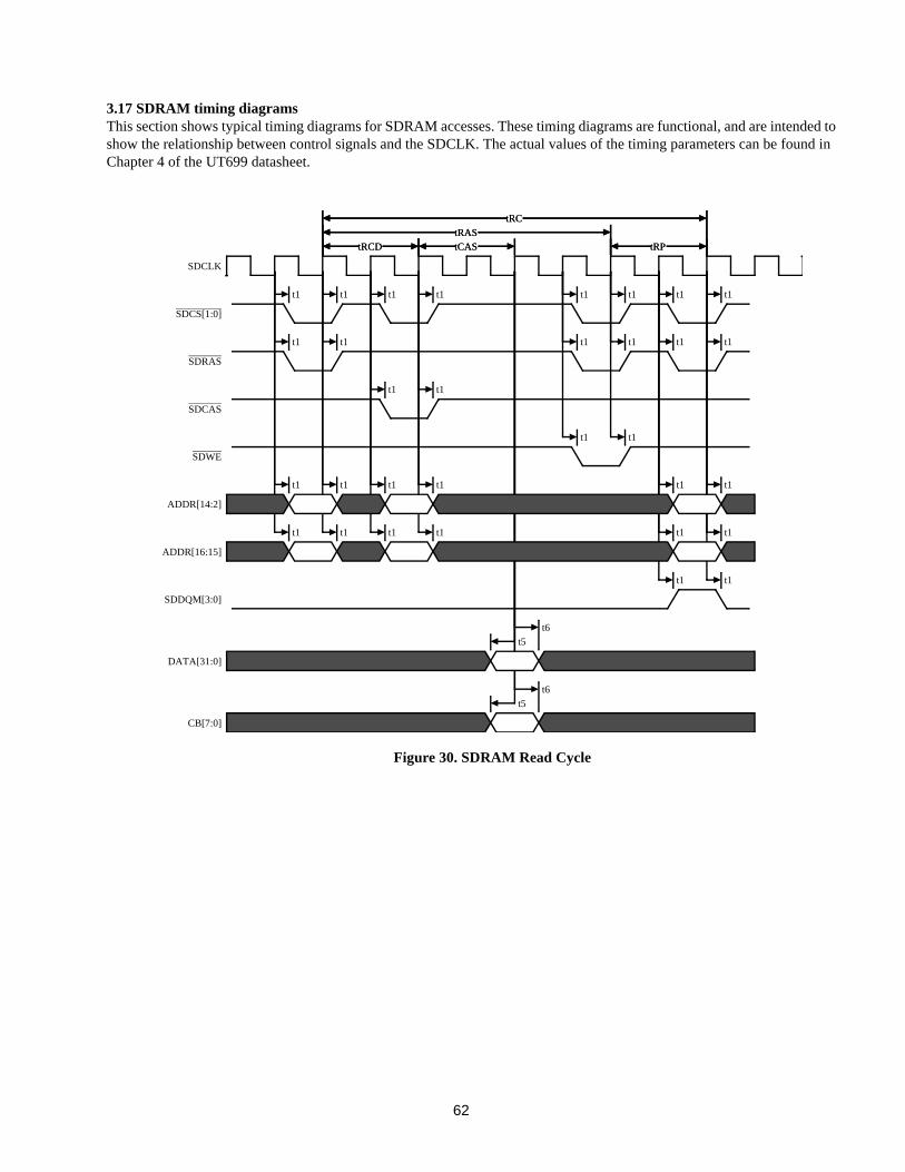
62
3.17 SDRAM timing diagramsThis section shows typical timing diagrams for SDRAM accesses. These timing diagrams are functional, and are intended to show the relationship between control signals and the SDCLK. The actual values of the timing parameters can be found in Chapter 4 of the UT699 datasheet.
t6
t5
t6t5
t1t1
t1t1t1t1t1t1
t1t1t1t1t1t1
t1t1
t1t1
t1t1t1t1t1t1
t1t1t1t1t1t1t1t1
tRC
tRPtRAS
tRPtCAStCAStRCD
tRC
tRAStRCD
SDCLK
SDCS[1:0]
SDRAS
SDCAS
SDWE
ADDR[14:2]
ADDR[16:15]
SDDQM[3:0]
DATA[31:0]
CB[7:0]
Figure 30. SDRAM Read Cycle
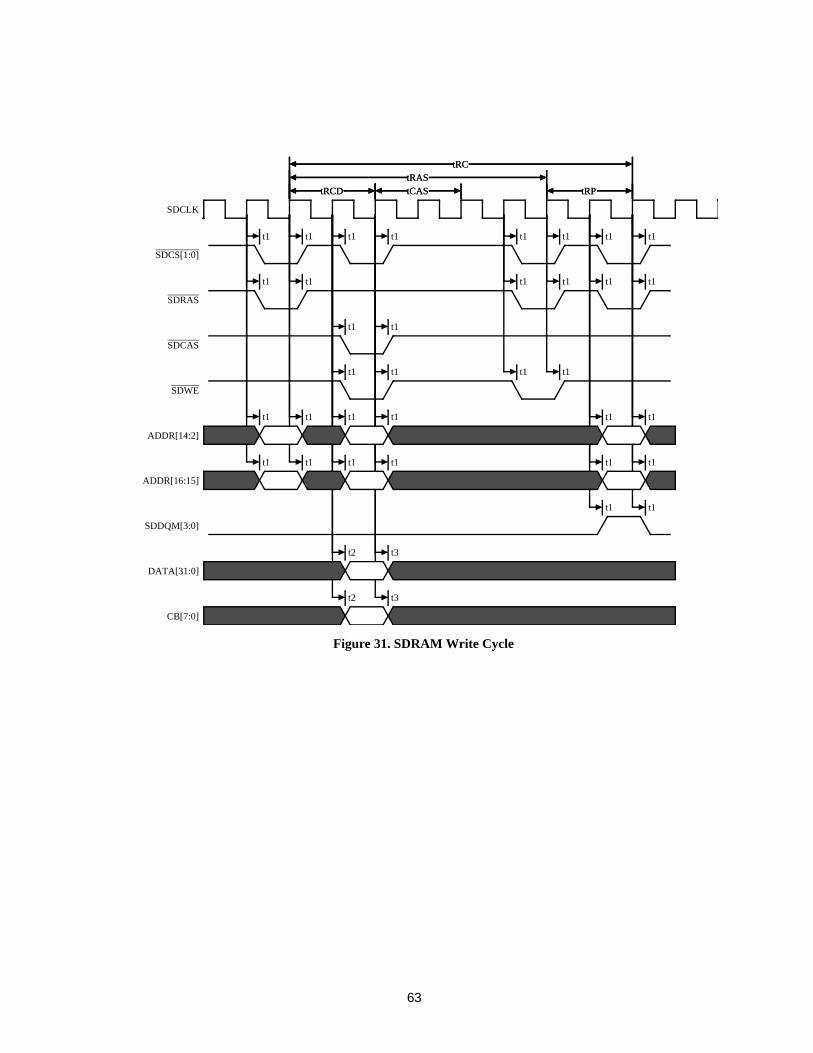
63
t3t2
t3t2
t1t1
t1t1t1t1t1t1
t1t1t1t1t1t1
t1t1t1t1
t1t1
t1t1t1t1t1t1
t1t1t1t1t1t1t1t1
tRC
tRPtRAS
tRPtCAStCAStRCD
tRCtRAS
tRCD
SDCLK
SDCS[1:0]
SDRAS
SDCAS
SDWE
ADDR[14:2]
ADDR[16:15]
SDDQM[3:0]
DATA[31:0]
CB[7:0]
Figure 31. SDRAM Write Cycle
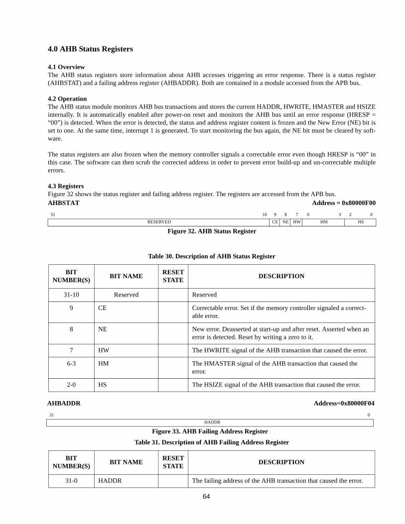
64
4.0 AHB Status Registers
4.1 OverviewThe AHB status registers store information about AHB accesses triggering an error response. There is a status register(AHBSTAT) and a failing address register (AHBADDR). Both are contained in a module accessed from the APB bus.
4.2 OperationThe AHB status module monitors AHB bus transactions and stores the current HADDR, HWRITE, HMASTER and HSIZEinternally. It is automatically enabled after power-on reset and monitors the AHB bus until an error response (HRESP =“00”) is detected. When the error is detected, the status and address register content is frozen and the New Error (NE) bit isset to one. At the same time, interrupt 1 is generated. To start monitoring the bus again, the NE bit must be cleared by soft-ware.
The status registers are also frozen when the memory controller signals a correctable error even though HRESP is “00” inthis case. The software can then scrub the corrected address in order to prevent error build-up and un-correctable multipleerrors.
4.3 RegistersFigure 32 shows the status register and failing address register. The registers are accessed from the APB bus. AHBSTAT Address = 0x80000F00
31 10 9 8 7 6 3 2 0
RESERVED CE NE HW HM HS
Figure 32. AHB Status Register
Table 30. Description of AHB Status Register
BIT NUMBER(S)
BIT NAMERESET STATE
DESCRIPTION
31-10 Reserved Reserved
9 CE Correctable error. Set if the memory controller signaled a correct-able error.
8 NE New error. Deasserted at start-up and after reset. Asserted when an error is detected. Reset by writing a zero to it.
7 HW The HWRITE signal of the AHB transaction that caused the error.
6-3 HM The HMASTER signal of the AHB transaction that caused the error.
2-0 HS The HSIZE signal of the AHB transaction that caused the error.
Table 31. Description of AHB Failing Address Register
BIT NUMBER(S)
BIT NAMERESET STATE
DESCRIPTION
31-0 HADDR The failing address of the AHB transaction that caused the error.
AHBADDR Address=0x80000F04
31 0
HADDR
Figure 33. AHB Failing Address Register
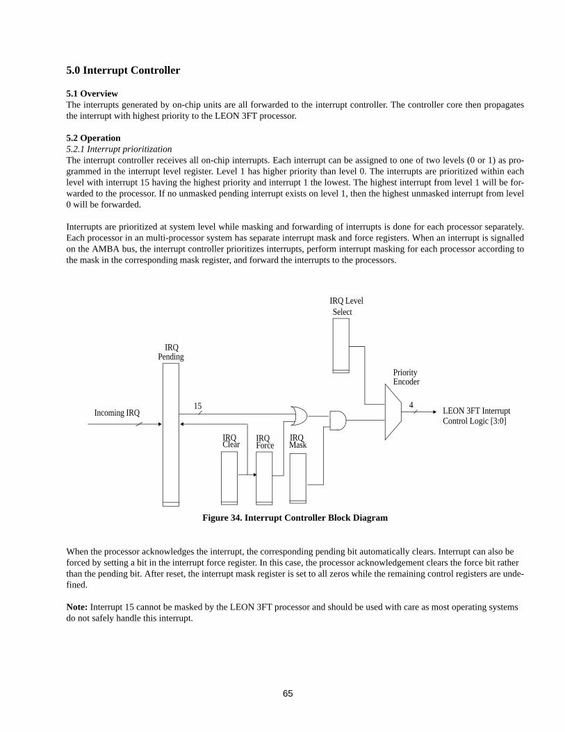
65
5.0 Interrupt Controller
5.1 OverviewThe interrupts generated by on-chip units are all forwarded to the interrupt controller. The controller core then propagatesthe interrupt with highest priority to the LEON 3FT processor.
5.2 Operation5.2.1 Interrupt prioritizationThe interrupt controller receives all on-chip interrupts. Each interrupt can be assigned to one of two levels (0 or 1) as pro-grammed in the interrupt level register. Level 1 has higher priority than level 0. The interrupts are prioritized within eachlevel with interrupt 15 having the highest priority and interrupt 1 the lowest. The highest interrupt from level 1 will be for-warded to the processor. If no unmasked pending interrupt exists on level 1, then the highest unmasked interrupt from level0 will be forwarded.
Interrupts are prioritized at system level while masking and forwarding of interrupts is done for each processor separately.Each processor in an multi-processor system has separate interrupt mask and force registers. When an interrupt is signalledon the AMBA bus, the interrupt controller prioritizes interrupts, perform interrupt masking for each processor according tothe mask in the corresponding mask register, and forward the interrupts to the processors.
When the processor acknowledges the interrupt, the corresponding pending bit automatically clears. Interrupt can also be forced by setting a bit in the interrupt force register. In this case, the processor acknowledgement clears the force bit rather than the pending bit. After reset, the interrupt mask register is set to all zeros while the remaining control registers are unde-fined.
Note: Interrupt 15 cannot be masked by the LEON 3FT processor and should be used with care as most operating systems do not safely handle this interrupt.
Figure 34. Interrupt Controller Block Diagram
IRQPending
15 4LEON 3FT Interrupt
IRQ LevelSelect
IRQMask
IRQForce
PriorityEncoder
Incoming IRQControl Logic [3:0]
IRQClear
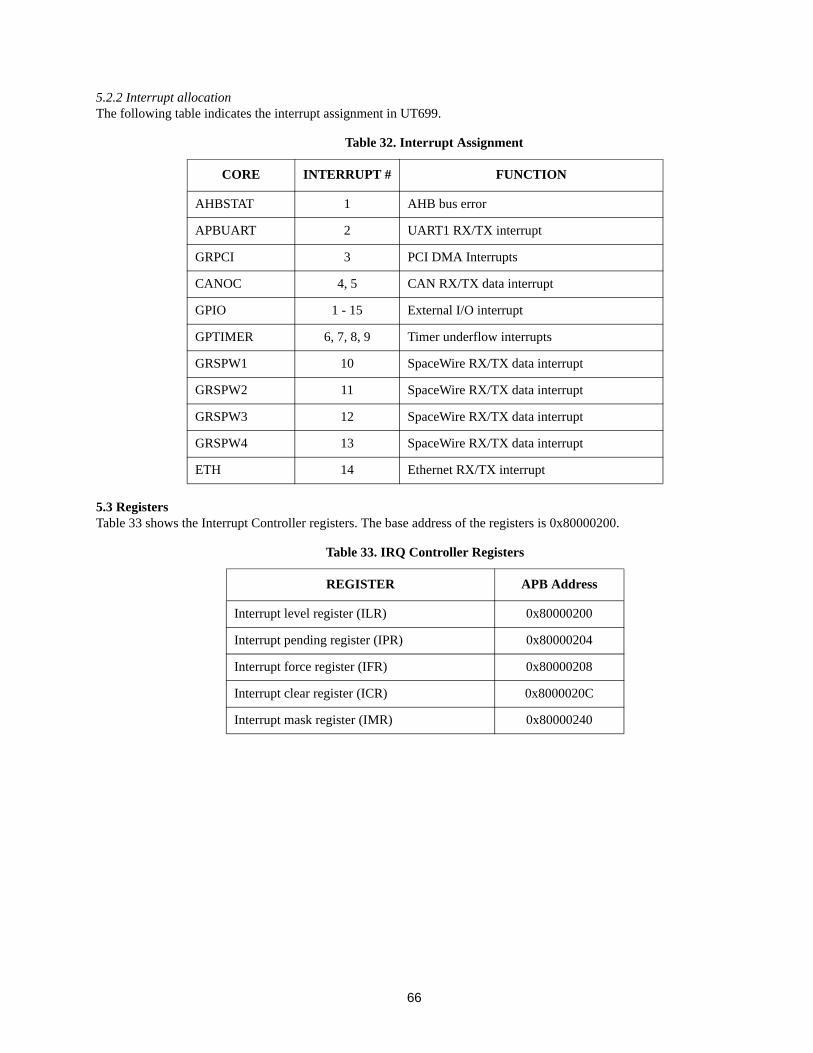
66
5.2.2 Interrupt allocationThe following table indicates the interrupt assignment in UT699.
5.3 RegistersTable 33 shows the Interrupt Controller registers. The base address of the registers is 0x80000200.
Table 32. Interrupt Assignment
CORE INTERRUPT # FUNCTION
AHBSTAT 1 AHB bus error
APBUART 2 UART1 RX/TX interrupt
GRPCI 3 PCI DMA Interrupts
CANOC 4, 5 CAN RX/TX data interrupt
GPIO 1 - 15 External I/O interrupt
GPTIMER 6, 7, 8, 9 Timer underflow interrupts
GRSPW1 10 SpaceWire RX/TX data interrupt
GRSPW2 11 SpaceWire RX/TX data interrupt
GRSPW3 12 SpaceWire RX/TX data interrupt
GRSPW4 13 SpaceWire RX/TX data interrupt
ETH 14 Ethernet RX/TX interrupt
Table 33. IRQ Controller Registers
REGISTER APB Address
Interrupt level register (ILR) 0x80000200
Interrupt pending register (IPR) 0x80000204
Interrupt force register (IFR) 0x80000208
Interrupt clear register (ICR) 0x8000020C
Interrupt mask register (IMR) 0x80000240
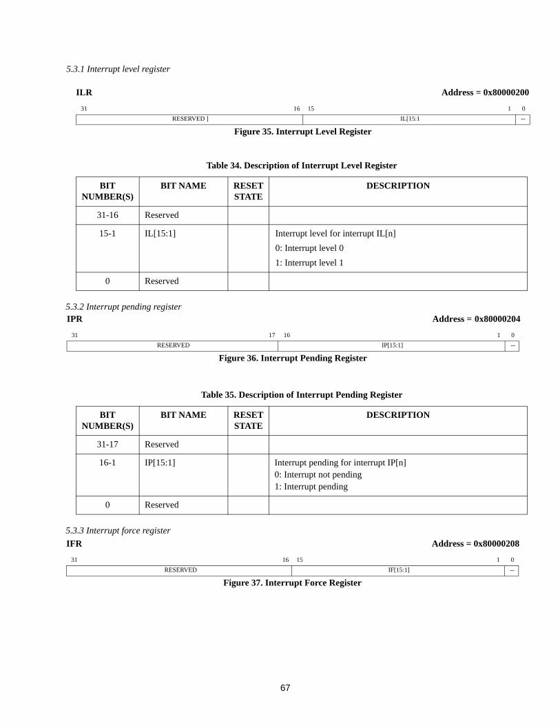
67
5.3.1 Interrupt level register
5.3.2 Interrupt pending register
5.3.3 Interrupt force register
Table 34. Description of Interrupt Level Register
BIT NUMBER(S)
BIT NAME RESET STATE
DESCRIPTION
31-16 Reserved
15-1 IL[15:1] Interrupt level for interrupt IL[n]
0: Interrupt level 0
1: Interrupt level 1
0 Reserved
Table 35. Description of Interrupt Pending Register
BIT NUMBER(S)
BIT NAME RESET STATE
DESCRIPTION
31-17 Reserved
16-1 IP[15:1] Interrupt pending for interrupt IP[n]0: Interrupt not pending1: Interrupt pending
0 Reserved
ILR Address = 0x80000200
31 16 15 1 0
RESERVED ] IL[15:1 --
Figure 35. Interrupt Level Register
IPR Address = 0x80000204
31 17 16 1 0
RESERVED IP[15:1] --
Figure 36. Interrupt Pending Register
IFR Address = 0x80000208
31 16 15 1 0
RESERVED IF[15:1] --
Figure 37. Interrupt Force Register
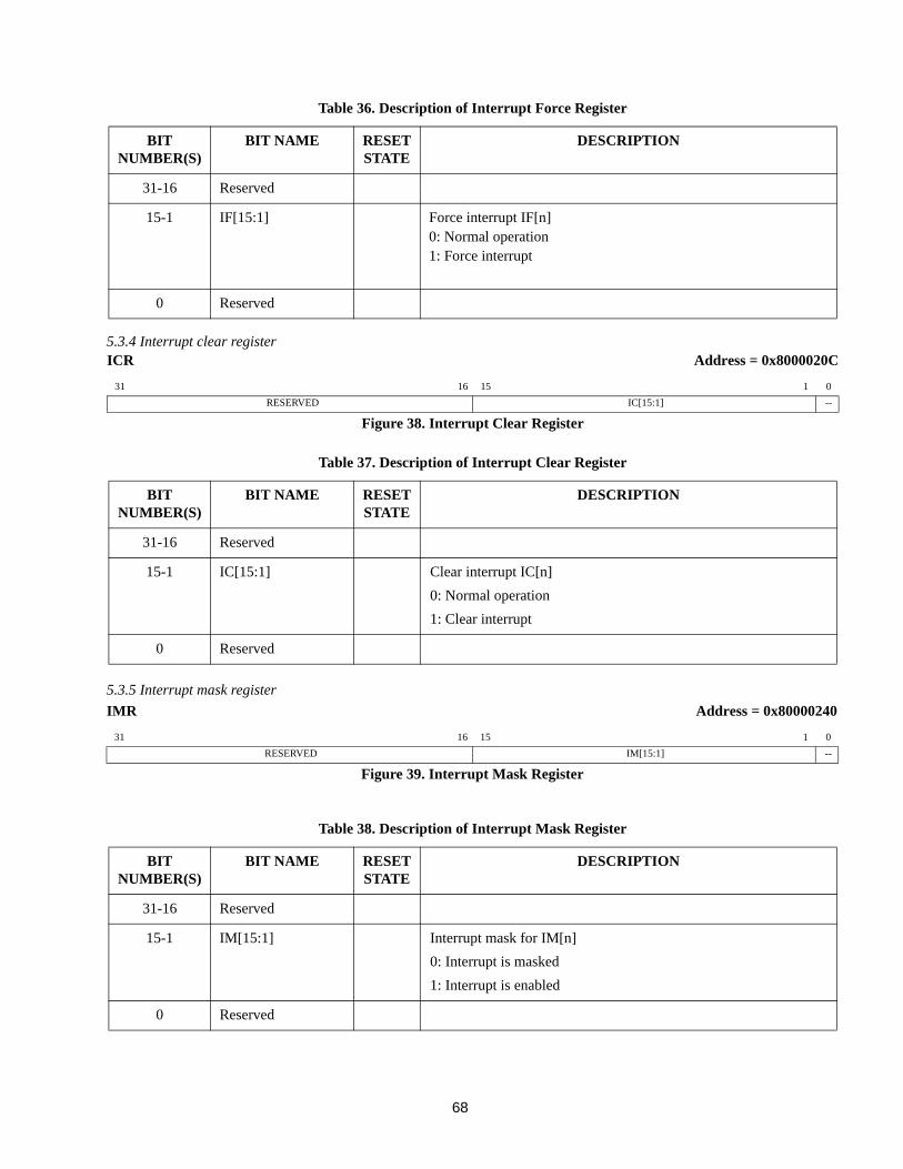
68
5.3.4 Interrupt clear register
5.3.5 Interrupt mask register
Table 36. Description of Interrupt Force Register
BIT NUMBER(S)
BIT NAME RESET STATE
DESCRIPTION
31-16 Reserved
15-1 IF[15:1] Force interrupt IF[n]0: Normal operation1: Force interrupt
0 Reserved
Table 37. Description of Interrupt Clear Register
BIT NUMBER(S)
BIT NAME RESET STATE
DESCRIPTION
31-16 Reserved
15-1 IC[15:1] Clear interrupt IC[n]
0: Normal operation
1: Clear interrupt
0 Reserved
Table 38. Description of Interrupt Mask Register
BIT NUMBER(S)
BIT NAME RESET STATE
DESCRIPTION
31-16 Reserved
15-1 IM[15:1] Interrupt mask for IM[n]
0: Interrupt is masked
1: Interrupt is enabled
0 Reserved
ICR Address = 0x8000020C
31 16 15 1 0
RESERVED IC[15:1] --
Figure 38. Interrupt Clear Register
IMR Address = 0x80000240
31 16 15 1 0
RESERVED IM[15:1] --
Figure 39. Interrupt Mask Register
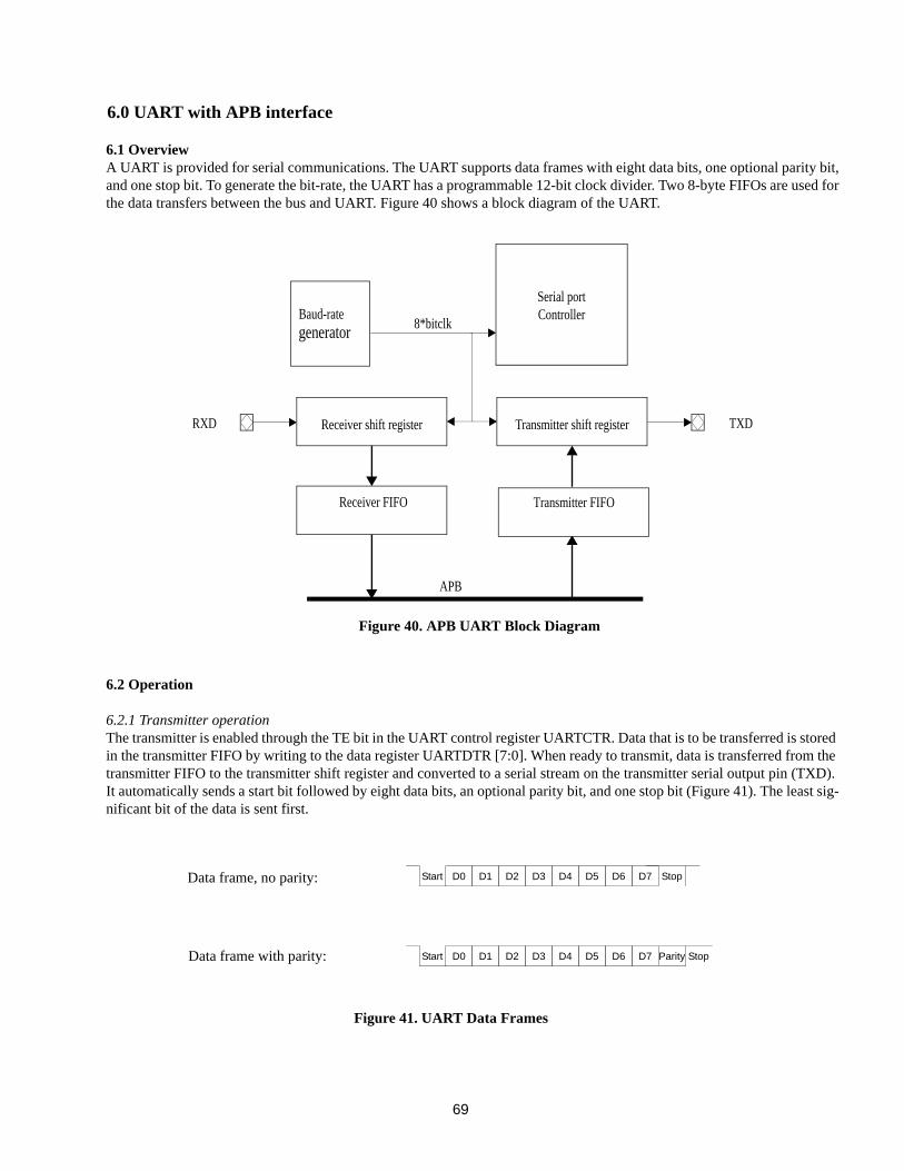
69
6.0 UART with APB interface
6.1 OverviewA UART is provided for serial communications. The UART supports data frames with eight data bits, one optional parity bit,and one stop bit. To generate the bit-rate, the UART has a programmable 12-bit clock divider. Two 8-byte FIFOs are used forthe data transfers between the bus and UART. Figure 40 shows a block diagram of the UART.
6.2 Operation
6.2.1 Transmitter operationThe transmitter is enabled through the TE bit in the UART control register UARTCTR. Data that is to be transferred is stored in the transmitter FIFO by writing to the data register UARTDTR [7:0]. When ready to transmit, data is transferred from the transmitter FIFO to the transmitter shift register and converted to a serial stream on the transmitter serial output pin (TXD). It automatically sends a start bit followed by eight data bits, an optional parity bit, and one stop bit (Figure 41). The least sig-nificant bit of the data is sent first.
RXD TXDReceiver shift register Transmitter shift register
APB
Serial portController
8*bitclkBaud-rategenerator
Transmitter FIFO
Receiver FIFO
Figure 40. APB UART Block Diagram
Start D0 StopD6D5D4D3D2D1 D7
Start D0 D6D5D4D3D2D1 D7 StopParity
Data frame, no parity:
Data frame with parity:
Figure 41. UART Data Frames
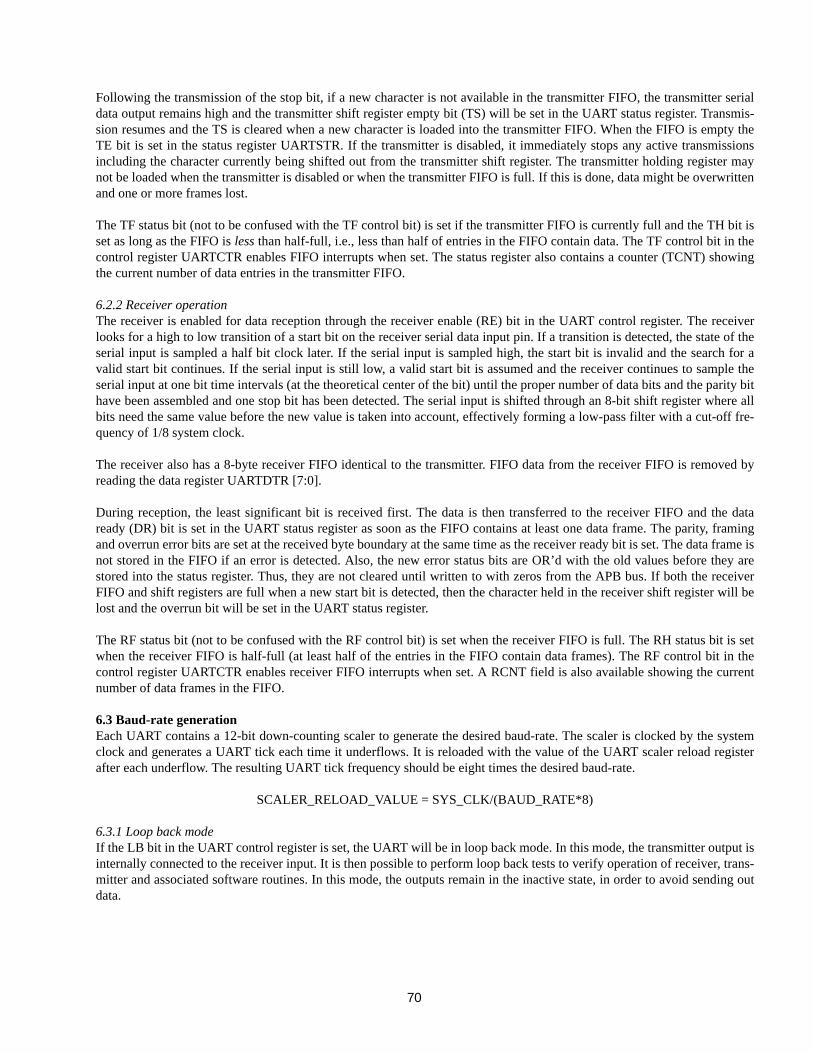
70
Following the transmission of the stop bit, if a new character is not available in the transmitter FIFO, the transmitter serialdata output remains high and the transmitter shift register empty bit (TS) will be set in the UART status register. Transmis-sion resumes and the TS is cleared when a new character is loaded into the transmitter FIFO. When the FIFO is empty theTE bit is set in the status register UARTSTR. If the transmitter is disabled, it immediately stops any active transmissionsincluding the character currently being shifted out from the transmitter shift register. The transmitter holding register maynot be loaded when the transmitter is disabled or when the transmitter FIFO is full. If this is done, data might be overwrittenand one or more frames lost.
The TF status bit (not to be confused with the TF control bit) is set if the transmitter FIFO is currently full and the TH bit isset as long as the FIFO is less than half-full, i.e., less than half of entries in the FIFO contain data. The TF control bit in thecontrol register UARTCTR enables FIFO interrupts when set. The status register also contains a counter (TCNT) showingthe current number of data entries in the transmitter FIFO.
6.2.2 Receiver operationThe receiver is enabled for data reception through the receiver enable (RE) bit in the UART control register. The receiverlooks for a high to low transition of a start bit on the receiver serial data input pin. If a transition is detected, the state of theserial input is sampled a half bit clock later. If the serial input is sampled high, the start bit is invalid and the search for avalid start bit continues. If the serial input is still low, a valid start bit is assumed and the receiver continues to sample theserial input at one bit time intervals (at the theoretical center of the bit) until the proper number of data bits and the parity bithave been assembled and one stop bit has been detected. The serial input is shifted through an 8-bit shift register where allbits need the same value before the new value is taken into account, effectively forming a low-pass filter with a cut-off fre-quency of 1/8 system clock.
The receiver also has a 8-byte receiver FIFO identical to the transmitter. FIFO data from the receiver FIFO is removed byreading the data register UARTDTR [7:0].
During reception, the least significant bit is received first. The data is then transferred to the receiver FIFO and the dataready (DR) bit is set in the UART status register as soon as the FIFO contains at least one data frame. The parity, framingand overrun error bits are set at the received byte boundary at the same time as the receiver ready bit is set. The data frame isnot stored in the FIFO if an error is detected. Also, the new error status bits are OR’d with the old values before they arestored into the status register. Thus, they are not cleared until written to with zeros from the APB bus. If both the receiverFIFO and shift registers are full when a new start bit is detected, then the character held in the receiver shift register will belost and the overrun bit will be set in the UART status register.
The RF status bit (not to be confused with the RF control bit) is set when the receiver FIFO is full. The RH status bit is setwhen the receiver FIFO is half-full (at least half of the entries in the FIFO contain data frames). The RF control bit in thecontrol register UARTCTR enables receiver FIFO interrupts when set. A RCNT field is also available showing the currentnumber of data frames in the FIFO.
6.3 Baud-rate generationEach UART contains a 12-bit down-counting scaler to generate the desired baud-rate. The scaler is clocked by the systemclock and generates a UART tick each time it underflows. It is reloaded with the value of the UART scaler reload registerafter each underflow. The resulting UART tick frequency should be eight times the desired baud-rate.
SCALER_RELOAD_VALUE = SYS_CLK/(BAUD_RATE*8)
6.3.1 Loop back modeIf the LB bit in the UART control register is set, the UART will be in loop back mode. In this mode, the transmitter output isinternally connected to the receiver input. It is then possible to perform loop back tests to verify operation of receiver, trans-mitter and associated software routines. In this mode, the outputs remain in the inactive state, in order to avoid sending outdata.
71
6.3.2. Interrupt generationTwo different kinds of interrupts are available: normal interrupts and FIFO interrupts. For the transmitter, normal interruptsare generated when transmitter interrupts are enabled (TI), the transmitter is enabled and the transmitter FIFO goes fromcontaining data to being empty. FIFO interrupts are generated when the FIFO interrupts are enabled (TF), transmissions areenabled (TE) and the UART is less than half-full (that is, whenever the TH status bit is set). This is a level interrupt and theinterrupt signal is continuously driven high as long as the condition prevails. The receiver interrupts work in the same way.Normal interrupts are generated in the same manner as for the holding register. FIFO interrupts are generated when receiverFIFO interrupts are enabled, the receiver is enabled and the FIFO is half-full. The interrupt signal is continuously drivenhigh as long as the receiver FIFO is half-full (at least half of the entries contain data frames).
6.4 UART registersThe APB UART is controlled through four registers mapped into APB address space. UART registers are mapped as fol-lows:
6.4.1 UART data registerThe UART data register provides access to the receiver and transmit FIFO register. The transmitter FIFO is accessed by writing to the data register; the receiver FIFO is accessed by reading the data register.
UARTDTR Address=0x80000100
6.4.2 UART status registerThe UART Status Register provides information about the state of the FIFO’s and error conditions.
UARTSTR Address=0x80000104
Table 39. APB UART Registers
REGISTER APB ADDRESS
UART Data Register (UARTDTR) 0x80000100
UART Status Register (UARTSTR) 0x80000104
UART Control Register (UARTCTR) 0x80000108
UART Scaler Register (UARTSCR) 0x8000010C
31 8 7 0
RESERVED DATA[7:0]
Figure 42. UART Data Register
Table 40. Description of UART Data Register
BIT NUMBER
BIT NAME RESET STATE
DESCRIPTION
31-8 Reserved
7-0 Receiver FIFO Reading the data register accesses the receiver FIFO.
7-0 Transmitter FIFO Writing to the data register access the transmitter FIFO.
31 26 25 20 19 11 10 9 8 7 6 5 4 3 2 1 0
RCNT TCNT RESERVED RF TF RH TH FE PE OV BR TE TS DR
Figure 43. UART Status Register
72
6.4.3 UART control registerThe UART Control Register is used to enable the transmitter and receiver and control how interrupts are generated.UARTCTR Address=0x80000108
Table 41. Description of UART Status Register
BIT NUMBER(S)
BIT NAME RESET STATE
DESCRIPTION
31-26 RCNT Receiver FIFO CountShows the number of data frames in the Receiver FIFO.
25-20 TCNT Transmitter FIFO CountShows the number of data frames in the Transmitter FIFO.
19-11 Reserved
10 RF Receiver FIFO FullIndicates that the Receiver FIFO is full.
9 TF Transmitter FIFO FullIndicates that the Transmitter FIFO is full.
8 RH Receiver FIFO Half FullIndicates that at least half of the FIFO is holding data.
7 TH Transmitter FIFO Half FullIndicates that the FIFO is less than half-full.
6 FE Framing ErrorIndicates that a framing error was detected.
5 PE Parity ErrorIndicates that a parity error was detected.
4 OV OverrunIndicates that one or more characters have been lost due to overrun.
3 BR Break ReceivedIndicates that a BREAK has been received.
2 TE Transmitter FIFO EmptyIndicates that the transmitter FIFO is empty.
1 TS Transmitter Shift Register EmptyIndicates that the transmitter shift register is empty.
0 DR Data ReadyIndicates that new data is available in the receiver holding register.
31 11 10 9 8 7 6 5 4 3 2 1 0
RESERVED RF TF -- LB -- PE PS TI RI TE RE
Figure 44. UART Control Register
Table 42. Description of UART Control Register
BIT NUMBER(S)
BIT NAME RESET STATE
DESCRIPTION
31-11 Reserved
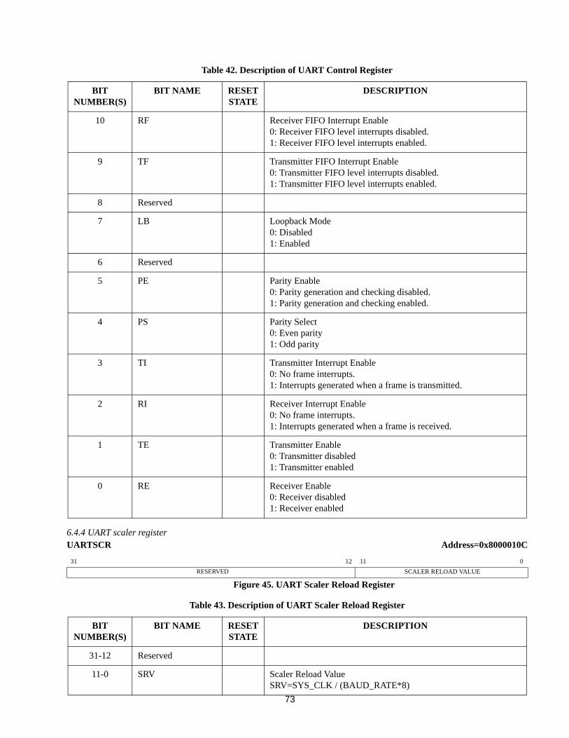
73
6.4.4 UART scaler registerUARTSCR Address=0x8000010C
BIT NUMBER(S)
BIT NAME RESET STATE
DESCRIPTION
10 RF Receiver FIFO Interrupt Enable0: Receiver FIFO level interrupts disabled.1: Receiver FIFO level interrupts enabled.
9 TF Transmitter FIFO Interrupt Enable0: Transmitter FIFO level interrupts disabled.1: Transmitter FIFO level interrupts enabled.
8 Reserved
7 LB Loopback Mode0: Disabled1: Enabled
6 Reserved
5 PE Parity Enable0: Parity generation and checking disabled.1: Parity generation and checking enabled.
4 PS Parity Select0: Even parity1: Odd parity
3 TI Transmitter Interrupt Enable0: No frame interrupts.1: Interrupts generated when a frame is transmitted.
2 RI Receiver Interrupt Enable0: No frame interrupts.1: Interrupts generated when a frame is received.
1 TE Transmitter Enable0: Transmitter disabled1: Transmitter enabled
0 RE Receiver Enable0: Receiver disabled1: Receiver enabled
31 12 11 0
RESERVED SCALER RELOAD VALUE
Figure 45. UART Scaler Reload Register
Table 43. Description of UART Scaler Reload Register
BIT NUMBER(S)
BIT NAME RESET STATE
DESCRIPTION
31-12 Reserved
11-0 SRV Scaler Reload ValueSRV=SYS_CLK / (BAUD_RATE*8)
Table 42. Description of UART Control Register
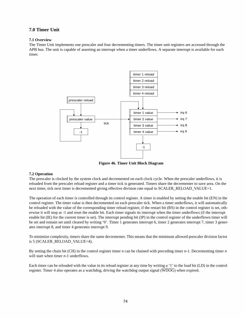
74
7.0 Timer Unit
7.1 OverviewThe Timer Unit implements one prescaler and four decrementing timers. The timer unit registers are accessed through the APB bus. The unit is capable of asserting an interrupt when a timer underflows. A separate interrupt is available for each timer.
7.2 OperationThe prescaler is clocked by the system clock and decremented on each clock cycle. When the prescaler underflows, it is reloaded from the prescaler reload register and a timer tick is generated. Timers share the decrementer to save area. On the next timer, tick next timer is decremented giving effective division rate equal to SCALER_RELOAD_VALUE+1.
The operation of each timer is controlled through its control register. A timer is enabled by setting the enable bit (EN) in the control register. The timer value is then decremented on each prescaler tick. When a timer underflows, it will automatically be reloaded with the value of the corresponding timer reload register, if the restart bit (RS) in the control register is set, oth-erwise it will stop at -1 and reset the enable bit. Each timer signals its interrupt when the timer underflows (if the interrupt enable bit (IE) for the current timer is set). The interrupt pending bit (IP) in the control register of the underflown timer will be set and remain set until cleared by writing ‘0’. Timer 1 generates interrupt 6, timer 2 generates interrupt 7, timer 3 gener-ates interrupt 8, and timer 4 generates interrupt 9.
To minimize complexity, timers share the same decrementer. This means that the minimum allowed prescaler division factor is 5 (SCALER_RELOAD_VALUE=4).
By setting the chain bit (CH) in the control register timer n can be chained with preceding timer n-1. Decrementing timer n will start when timer n-1 underflows.
Each timer can be reloaded with the value in its reload register at any time by writing a ‘1’ to the load bit (LD) in the control register. Timer 4 also operates as a watchdog, driving the watchdog output signal (WDOG) when expired.
timer 3 reload
prescaler reload
-1
prescaler value
timer 1 value
timer 2 value
timer 3 value
timer 1 reload
timer 2 reload
-1
tick
irq 6
irq 7
irq 8
timer 4 reload
timer 4 value irq 9
Figure 46. Timer Unit Block Diagram
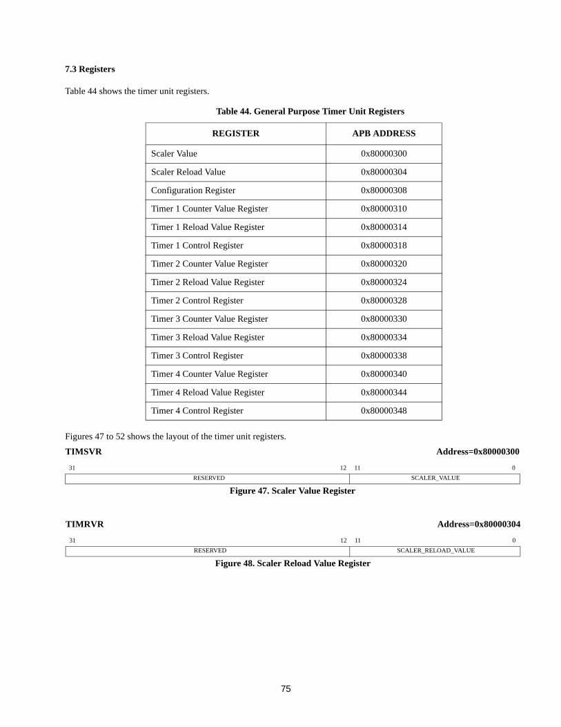
75
7.3 Registers
Table 44 shows the timer unit registers.
Figures 47 to 52 shows the layout of the timer unit registers.
Table 44. General Purpose Timer Unit Registers
REGISTER APB ADDRESS
Scaler Value 0x80000300
Scaler Reload Value 0x80000304
Configuration Register 0x80000308
Timer 1 Counter Value Register 0x80000310
Timer 1 Reload Value Register 0x80000314
Timer 1 Control Register 0x80000318
Timer 2 Counter Value Register 0x80000320
Timer 2 Reload Value Register 0x80000324
Timer 2 Control Register 0x80000328
Timer 3 Counter Value Register 0x80000330
Timer 3 Reload Value Register 0x80000334
Timer 3 Control Register 0x80000338
Timer 4 Counter Value Register 0x80000340
Timer 4 Reload Value Register 0x80000344
Timer 4 Control Register 0x80000348
TIMSVR Address=0x80000300
31 12 11 0
RESERVED SCALER_VALUE
Figure 47. Scaler Value Register
TIMRVR Address=0x80000304
31 12 11 0
RESERVED SCALER_RELOAD_VALUE
Figure 48. Scaler Reload Value Register
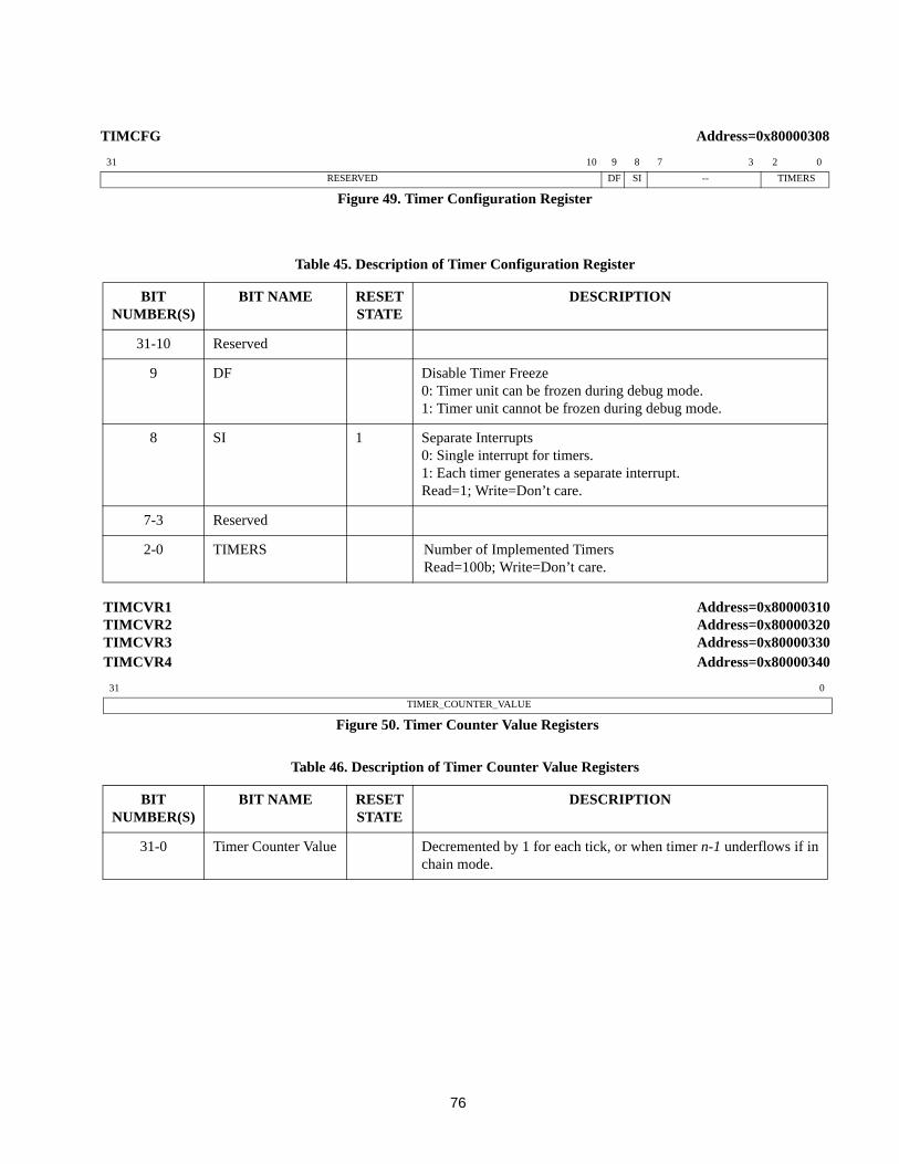
76
Table 45. Description of Timer Configuration Register
BIT NUMBER(S)
BIT NAME RESET STATE
DESCRIPTION
31-10 Reserved
9 DF Disable Timer Freeze0: Timer unit can be frozen during debug mode.1: Timer unit cannot be frozen during debug mode.
8 SI 1 Separate Interrupts0: Single interrupt for timers.1: Each timer generates a separate interrupt.Read=1; Write=Don’t care.
7-3 Reserved
2-0 TIMERS Number of Implemented TimersRead=100b; Write=Don’t care.
Table 46. Description of Timer Counter Value Registers
BIT NUMBER(S)
BIT NAME RESET STATE
DESCRIPTION
31-0 Timer Counter Value Decremented by 1 for each tick, or when timer n-1 underflows if inchain mode.
TIMCFG Address=0x80000308
31 10 9 8 7 3 2 0
RESERVED DF SI -- TIMERS
Figure 49. Timer Configuration Register
TIMCVR1 Address=0x80000310TIMCVR2 Address=0x80000320TIMCVR3 Address=0x80000330TIMCVR4 Address=0x80000340
31 0
TIMER_COUNTER_VALUE
Figure 50. Timer Counter Value Registers
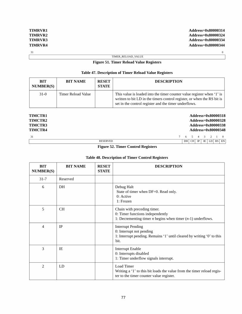
77
Table 47. Description of Timer Reload Value Registers
BIT NUMBER(S)
BIT NAME RESET STATE
DESCRIPTION
31-0 Timer Reload Value This value is loaded into the timer counter value register when ‘1’ iswritten to bit LD in the timers control register, or when the RS bit isset in the control register and the timer underflows.
Table 48. Description of Timer Control Registers
BIT NUMBER(S)
BIT NAME RESET STATE
DESCRIPTION
31-7 Reserved
6 DH Debug HaltState of timer when DF=0. Read only.0: Active1: Frozen
5 CH Chain with preceding timer.0: Timer functions independently1: Decrementing timer n begins when timer (n-1) underflows.
4 IP Interrupt Pending0: Interrupt not pending1: Interrupt pending. Remains ‘1’ until cleared by writing ‘0’ to this bit.
3 IE Interrupt Enable0: Interrupts disabled1: Timer underflow signals interrupt.
2 LD Load TimerWriting a ‘1’ to this bit loads the value from the timer reload regis-ter to the timer counter value register.
TIMRVR1 Address=0x80000314TIMRVR2 Address=0x80000324TIMRVR3 Address=0x80000334TIMRVR4 Address=0x80000344
31 0
TIMER_RELOAD_VALUE
Figure 51. Timer Reload Value Registers
TIMCTR1 Address=0x80000318TIMCTR2 Address=0x80000328TIMCTR3 Address=0x80000338TIMCTR4 Address=0x80000348
31 7 6 5 4 3 2 1 0
RESERVED DH CH IP IE LD RS EN
Figure 52. Timer Control Registers
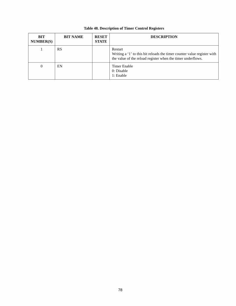
78
BIT NUMBER(S)
BIT NAME RESET STATE
DESCRIPTION
1 RS RestartWriting a ‘1’ to this bit reloads the timer counter value register withthe value of the reload register when the timer underflows.
0 EN Timer Enable0: Disable1: Enable
Table 48. Description of Timer Control Registers
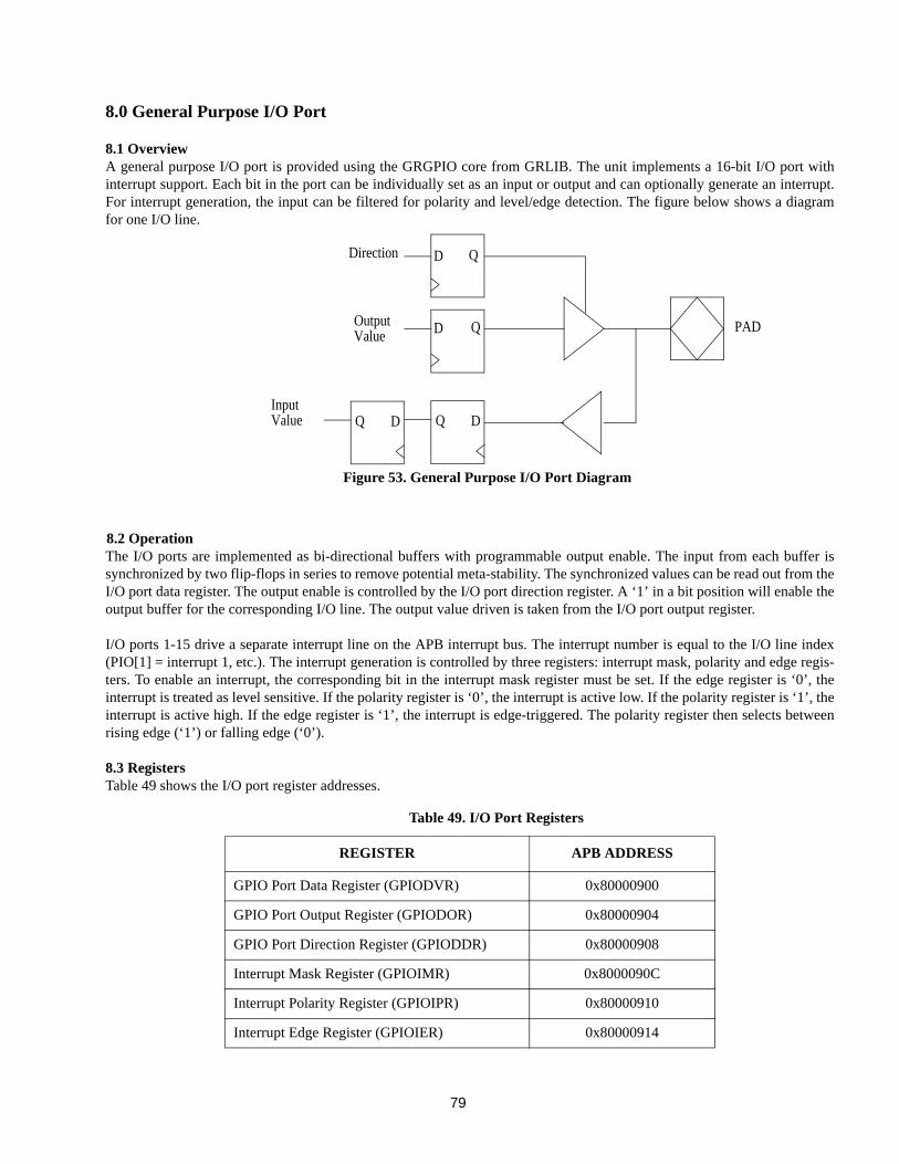
79
8.0 General Purpose I/O Port
8.1 OverviewA general purpose I/O port is provided using the GRGPIO core from GRLIB. The unit implements a 16-bit I/O port withinterrupt support. Each bit in the port can be individually set as an input or output and can optionally generate an interrupt.For interrupt generation, the input can be filtered for polarity and level/edge detection. The figure below shows a diagramfor one I/O line.
8.2 OperationThe I/O ports are implemented as bi-directional buffers with programmable output enable. The input from each buffer issynchronized by two flip-flops in series to remove potential meta-stability. The synchronized values can be read out from theI/O port data register. The output enable is controlled by the I/O port direction register. A ‘1’ in a bit position will enable theoutput buffer for the corresponding I/O line. The output value driven is taken from the I/O port output register.
I/O ports 1-15 drive a separate interrupt line on the APB interrupt bus. The interrupt number is equal to the I/O line index(PIO[1] = interrupt 1, etc.). The interrupt generation is controlled by three registers: interrupt mask, polarity and edge regis-ters. To enable an interrupt, the corresponding bit in the interrupt mask register must be set. If the edge register is ‘0’, theinterrupt is treated as level sensitive. If the polarity register is ‘0’, the interrupt is active low. If the polarity register is ‘1’, theinterrupt is active high. If the edge register is ‘1’, the interrupt is edge-triggered. The polarity register then selects betweenrising edge (‘1’) or falling edge (‘0’).
8.3 RegistersTable 49 shows the I/O port register addresses.
Table 49. I/O Port Registers
REGISTER APB ADDRESS
GPIO Port Data Register (GPIODVR) 0x80000900
GPIO Port Output Register (GPIODOR) 0x80000904
GPIO Port Direction Register (GPIODDR) 0x80000908
Interrupt Mask Register (GPIOIMR) 0x8000090C
Interrupt Polarity Register (GPIOIPR) 0x80000910
Interrupt Edge Register (GPIOIER) 0x80000914
Q
Q
Q
D
D
D PAD
Direction
OutputValue
InputValueQ D
InputValue
Figure 53. General Purpose I/O Port Diagram
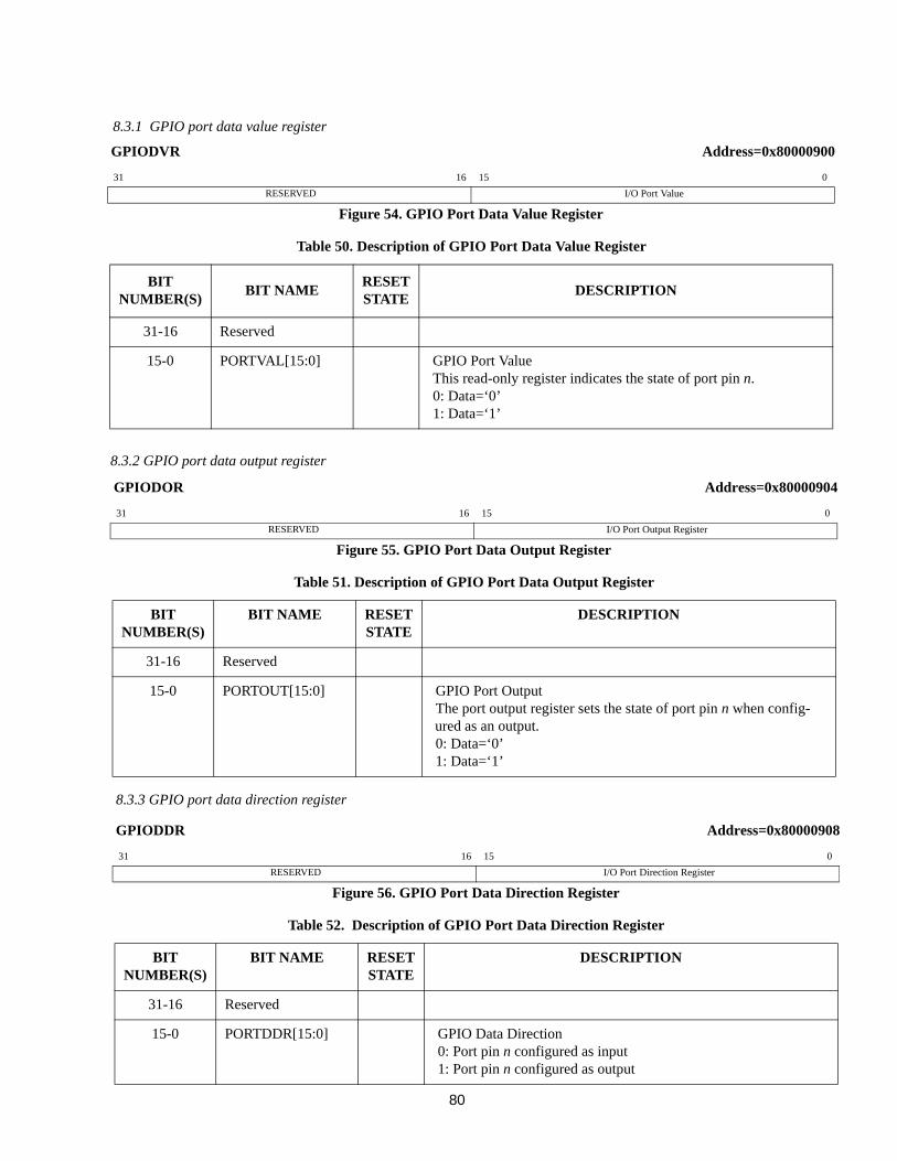
80
GPIODVR Address=0x80000900
31 16 15 0
RESERVED I/O Port Value
Figure 54. GPIO Port Data Value Register
Table 50. Description of GPIO Port Data Value Register
BIT NUMBER(S)
BIT NAMERESET STATE
DESCRIPTION
31-16 Reserved
15-0 PORTVAL[15:0] GPIO Port ValueThis read-only register indicates the state of port pin n.0: Data=‘0’1: Data=‘1’
GPIODOR Address=0x80000904
31 16 15 0
RESERVED I/O Port Output Register
Figure 55. GPIO Port Data Output Register
Table 51. Description of GPIO Port Data Output Register
BIT NUMBER(S)
BIT NAME RESET STATE
DESCRIPTION
31-16 Reserved
15-0 PORTOUT[15:0] GPIO Port OutputThe port output register sets the state of port pin n when config-ured as an output.0: Data=‘0’1: Data=‘1’
GPIODDR Address=0x80000908
31 16 15 0
RESERVED I/O Port Direction Register
Figure 56. GPIO Port Data Direction Register
Table 52. Description of GPIO Port Data Direction Register
BIT NUMBER(S)
BIT NAME RESET STATE
DESCRIPTION
31-16 Reserved
15-0 PORTDDR[15:0] GPIO Data Direction0: Port pin n configured as input1: Port pin n configured as output
8.3.2 GPIO port data output register
8.3.3 GPIO port data direction register
8.3.1 GPIO port data value register
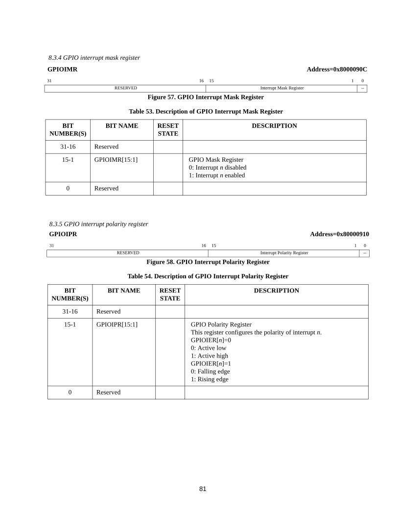
81
GPIOIMR Address=0x8000090C
31 16 15 1 0
RESERVED Interrupt Mask Register --
Figure 57. GPIO Interrupt Mask Register
Table 53. Description of GPIO Interrupt Mask Register
BIT NUMBER(S)
BIT NAME RESET STATE
DESCRIPTION
31-16 Reserved
15-1 GPIOIMR[15:1] GPIO Mask Register0: Interrupt n disabled1: Interrupt n enabled
0 Reserved
8.3.4 GPIO interrupt mask register
GPIOIPR Address=0x80000910
31 16 15 1 0
RESERVED Interrupt Polarity Register --
Figure 58. GPIO Interrupt Polarity Register
Table 54. Description of GPIO Interrupt Polarity Register
BIT NUMBER(S)
BIT NAME RESET STATE
DESCRIPTION
31-16 Reserved
15-1 GPIOIPR[15:1] GPIO Polarity RegisterThis register configures the polarity of interrupt n.GPIOIER[n]=00: Active low1: Active highGPIOIER[n]=10: Falling edge1: Rising edge
0 Reserved
8.3.5 GPIO interrupt polarity register
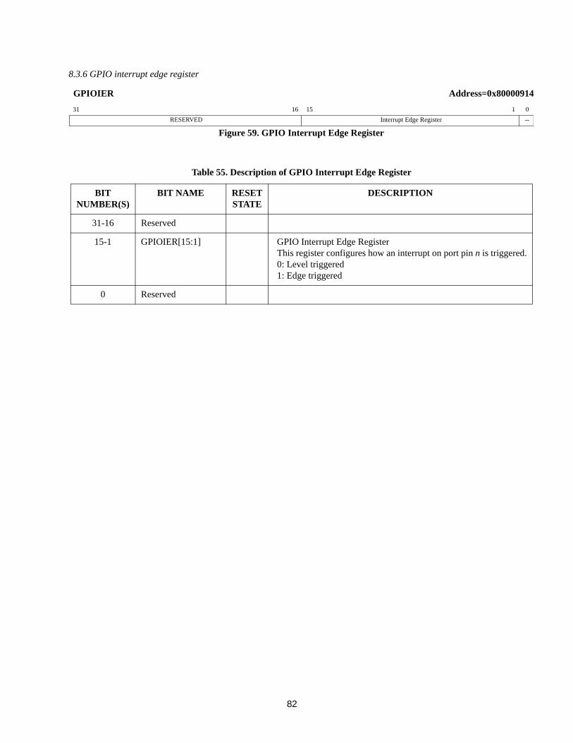
82
GPIOIER Address=0x80000914
31 16 15 1 0
RESERVED Interrupt Edge Register --
Figure 59. GPIO Interrupt Edge Register
Table 55. Description of GPIO Interrupt Edge Register
BIT NUMBER(S)
BIT NAME RESET STATE
DESCRIPTION
31-16 Reserved
15-1 GPIOIER[15:1] GPIO Interrupt Edge RegisterThis register configures how an interrupt on port pin n is triggered.0: Level triggered1: Edge triggered
0 Reserved
8.3.6 GPIO interrupt edge register
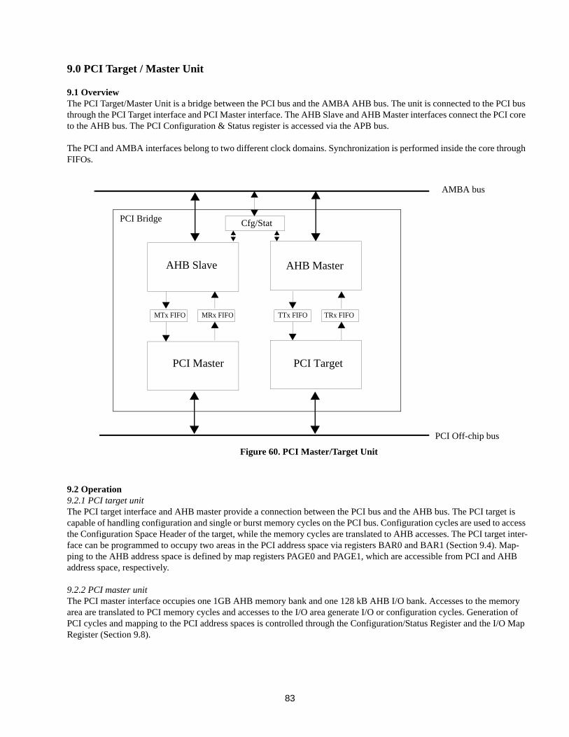
83
9.0 PCI Target / Master Unit
9.1 OverviewThe PCI Target/Master Unit is a bridge between the PCI bus and the AMBA AHB bus. The unit is connected to the PCI bus through the PCI Target interface and PCI Master interface. The AHB Slave and AHB Master interfaces connect the PCI core to the AHB bus. The PCI Configuration & Status register is accessed via the APB bus.
The PCI and AMBA interfaces belong to two different clock domains. Synchronization is performed inside the core through FIFOs.
9.2 Operation9.2.1 PCI target unitThe PCI target interface and AHB master provide a connection between the PCI bus and the AHB bus. The PCI target is capable of handling configuration and single or burst memory cycles on the PCI bus. Configuration cycles are used to access the Configuration Space Header of the target, while the memory cycles are translated to AHB accesses. The PCI target inter-face can be programmed to occupy two areas in the PCI address space via registers BAR0 and BAR1 (Section 9.4). Map-ping to the AHB address space is defined by map registers PAGE0 and PAGE1, which are accessible from PCI and AHB address space, respectively.
9.2.2 PCI master unitThe PCI master interface occupies one 1GB AHB memory bank and one 128 kB AHB I/O bank. Accesses to the memory area are translated to PCI memory cycles and accesses to the I/O area generate I/O or configuration cycles. Generation of PCI cycles and mapping to the PCI address spaces is controlled through the Configuration/Status Register and the I/O Map Register (Section 9.8).
PCI Master PCI Target
AHB Slave AHB Master
Cfg/Stat
AMBA bus
PCI Off-chip bus
PCI Bridge
MTx FIFO MRx FIFO TTx FIFO TRx FIFO
Figure 60. PCI Master/Target Unit
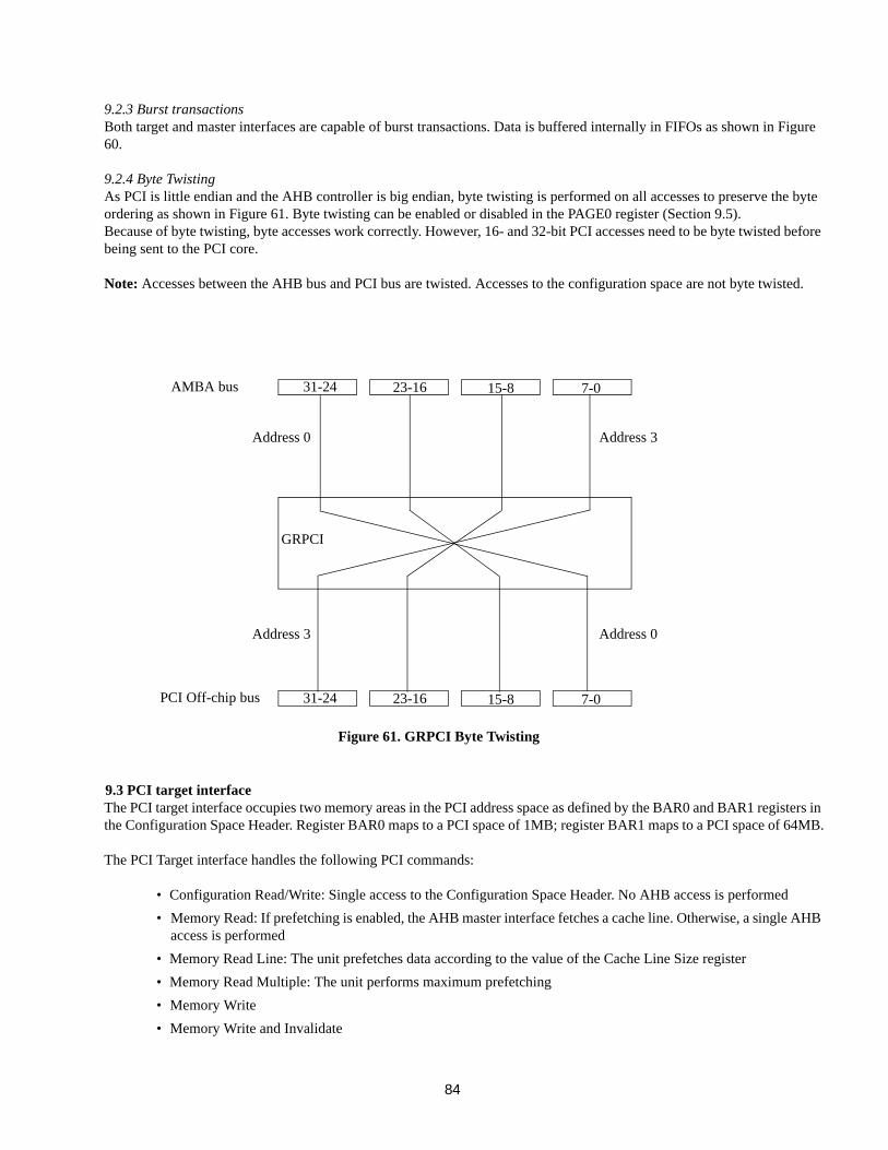
84
9.2.3 Burst transactionsBoth target and master interfaces are capable of burst transactions. Data is buffered internally in FIFOs as shown in Figure 60.
9.2.4 Byte TwistingAs PCI is little endian and the AHB controller is big endian, byte twisting is performed on all accesses to preserve the byte ordering as shown in Figure 61. Byte twisting can be enabled or disabled in the PAGE0 register (Section 9.5).Because of byte twisting, byte accesses work correctly. However, 16- and 32-bit PCI accesses need to be byte twisted before being sent to the PCI core.
Note: Accesses between the AHB bus and PCI bus are twisted. Accesses to the configuration space are not byte twisted.
9.3 PCI target interfaceThe PCI target interface occupies two memory areas in the PCI address space as defined by the BAR0 and BAR1 registers in the Configuration Space Header. Register BAR0 maps to a PCI space of 1MB; register BAR1 maps to a PCI space of 64MB.
The PCI Target interface handles the following PCI commands:
• Configuration Read/Write: Single access to the Configuration Space Header. No AHB access is performed
• Memory Read: If prefetching is enabled, the AHB master interface fetches a cache line. Otherwise, a single AHB access is performed
• Memory Read Line: The unit prefetches data according to the value of the Cache Line Size register
• Memory Read Multiple: The unit performs maximum prefetching
• Memory Write
• Memory Write and Invalidate
AMBA bus
PCI Off-chip bus 31-24 23-16 15-8 7-0
31-24 23-16 15-8 7-0
GRPCI
Address 0
Address 0
Address 3
Address 3
Figure 61. GRPCI Byte Twisting
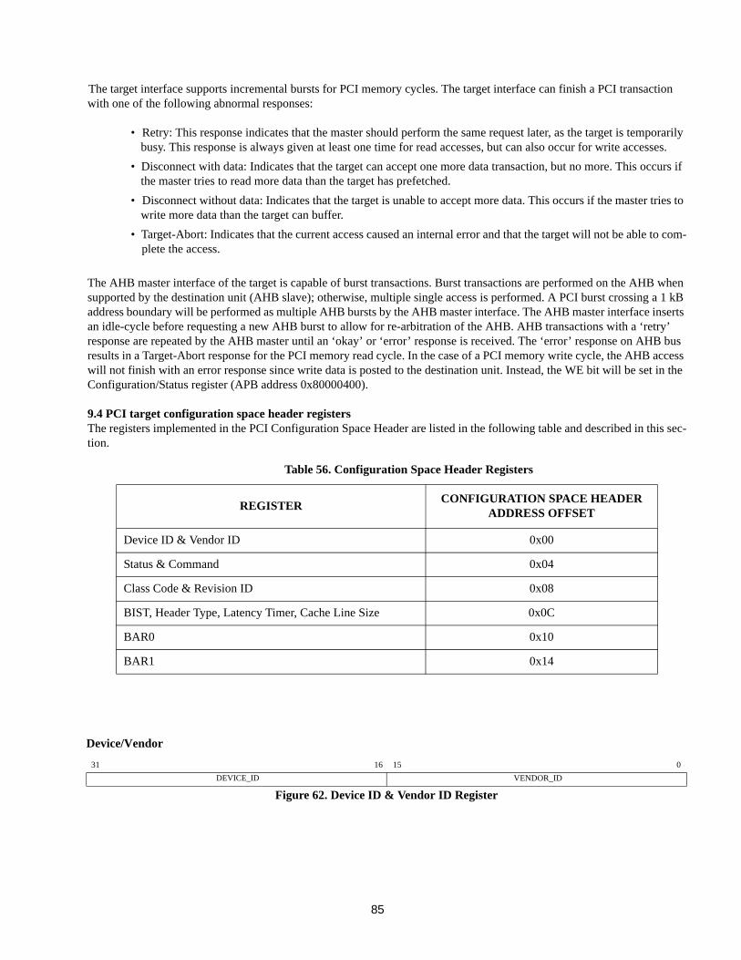
85
The target interface supports incremental bursts for PCI memory cycles. The target interface can finish a PCI transaction with one of the following abnormal responses:
• Retry: This response indicates that the master should perform the same request later, as the target is temporarily busy. This response is always given at least one time for read accesses, but can also occur for write accesses.
• Disconnect with data: Indicates that the target can accept one more data transaction, but no more. This occurs if the master tries to read more data than the target has prefetched.
• Disconnect without data: Indicates that the target is unable to accept more data. This occurs if the master tries to write more data than the target can buffer.
• Target-Abort: Indicates that the current access caused an internal error and that the target will not be able to com-plete the access.
The AHB master interface of the target is capable of burst transactions. Burst transactions are performed on the AHB when supported by the destination unit (AHB slave); otherwise, multiple single access is performed. A PCI burst crossing a 1 kB address boundary will be performed as multiple AHB bursts by the AHB master interface. The AHB master interface inserts an idle-cycle before requesting a new AHB burst to allow for re-arbitration of the AHB. AHB transactions with a ‘retry’ response are repeated by the AHB master until an ‘okay’ or ‘error’ response is received. The ‘error’ response on AHB bus results in a Target-Abort response for the PCI memory read cycle. In the case of a PCI memory write cycle, the AHB access will not finish with an error response since write data is posted to the destination unit. Instead, the WE bit will be set in the Configuration/Status register (APB address 0x80000400).
9.4 PCI target configuration space header registersThe registers implemented in the PCI Configuration Space Header are listed in the following table and described in this sec-tion.
Table 56. Configuration Space Header Registers
REGISTERCONFIGURATION SPACE HEADER
ADDRESS OFFSET
Device ID & Vendor ID 0x00
Status & Command 0x04
Class Code & Revision ID 0x08
BIST, Header Type, Latency Timer, Cache Line Size 0x0C
BAR0 0x10
BAR1 0x14
Device/Vendor
31 16 15 0
DEVICE_ID VENDOR_ID
Figure 62. Device ID & Vendor ID Register
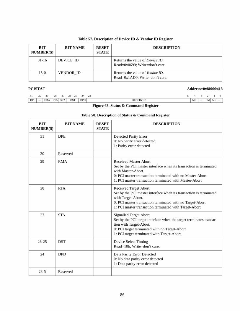
86
Table 57. Description of Device ID & Vendor ID Register
BIT NUMBER(S)
BIT NAME RESET STATE
DESCRIPTION
31-16 DEVICE_ID Returns the value of Device ID.Read=0x0699; Write=don’t care.
15-0 VENDOR_ID Returns the value of Vendor ID.Read=0x1AD0; Write=don’t care.
Table 58. Description of Status & Command Register
BIT NUMBER(S)
BIT NAME RESET STATE
DESCRIPTION
31 DPE Detected Parity Error0: No parity error detected1: Parity error detected
30 Reserved
29 RMA Received Master AbortSet by the PCI master interface when its transaction is terminated with Master-Abort.0: PCI master transaction terminated with no Master-Abort1: PCI master transaction terminated with Master-Abort
28 RTA Received Target AbortSet by the PCI master interface when its transaction is terminated with Target-Abort.0: PCI master transaction terminated with no Target-Abort1: PCI master transaction terminated with Target-Abort
27 STA Signalled Target AbortSet by the PCI target interface when the target terminates transac-tion with Target-Abort.0: PCI target terminated with no Target-Abort1: PCI target terminated with Target-Abort
26-25 DST Device Select TimingRead=10b; Write=don’t care.
24 DPD Data Parity Error Detected0: No data parity error detected1: Data parity error detected
23-5 Reserved
PCISTAT Address=0x80000418
31 30 29 28 27 26 25 24 23 5 4 3 2 1 0
DPE -- RMA RTA STA DST DPD RESERVED MIE -- BM MS --
Figure 63. Status & Command Register
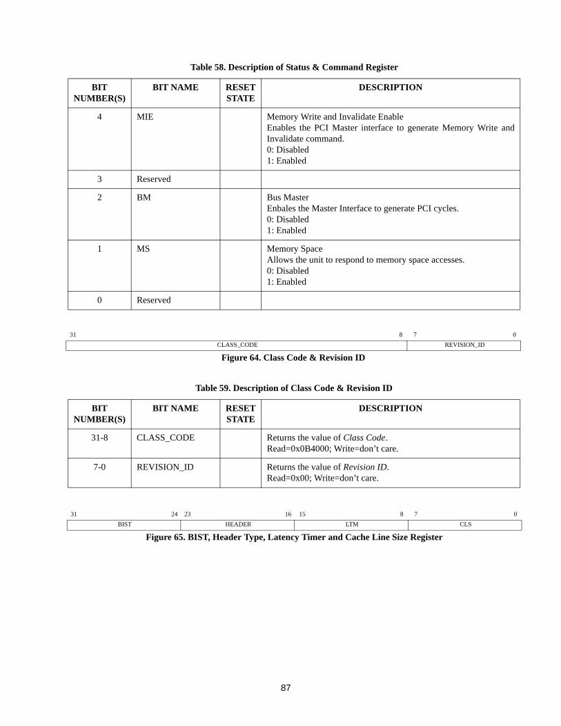
87
BIT NUMBER(S)
BIT NAME RESET STATE
DESCRIPTION
4 MIE Memory Write and Invalidate EnableEnables the PCI Master interface to generate Memory Write andInvalidate command.0: Disabled1: Enabled
3 Reserved
2 BM Bus MasterEnbales the Master Interface to generate PCI cycles.0: Disabled1: Enabled
1 MS Memory SpaceAllows the unit to respond to memory space accesses.0: Disabled1: Enabled
0 Reserved
Table 59. Description of Class Code & Revision ID
BIT NUMBER(S)
BIT NAME RESET STATE
DESCRIPTION
31-8 CLASS_CODE Returns the value of Class Code.Read=0x0B4000; Write=don’t care.
7-0 REVISION_ID Returns the value of Revision ID.Read=0x00; Write=don’t care.
Table 58. Description of Status & Command Register
31 8 7 0
CLASS_CODE REVISION_ID
Figure 64. Class Code & Revision ID
31 24 23 16 15 8 7 0
BIST HEADER LTM CLS
Figure 65. BIST, Header Type, Latency Timer and Cache Line Size Register
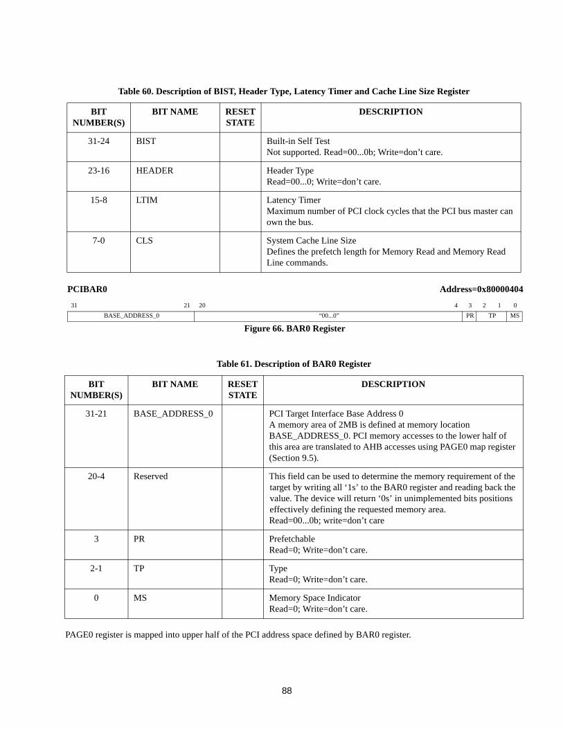
88
PAGE0 register is mapped into upper half of the PCI address space defined by BAR0 register.
Table 60. Description of BIST, Header Type, Latency Timer and Cache Line Size Register
BIT NUMBER(S)
BIT NAME RESET STATE
DESCRIPTION
31-24 BIST Built-in Self TestNot supported. Read=00...0b; Write=don’t care.
23-16 HEADER Header TypeRead=00...0; Write=don’t care.
15-8 LTIM Latency TimerMaximum number of PCI clock cycles that the PCI bus master can own the bus.
7-0 CLS System Cache Line SizeDefines the prefetch length for Memory Read and Memory Read Line commands.
Table 61. Description of BAR0 Register
BIT NUMBER(S)
BIT NAME RESET STATE
DESCRIPTION
31-21 BASE_ADDRESS_0 PCI Target Interface Base Address 0A memory area of 2MB is defined at memory location BASE_ADDRESS_0. PCI memory accesses to the lower half of this area are translated to AHB accesses using PAGE0 map register (Section 9.5).
20-4 Reserved This field can be used to determine the memory requirement of the target by writing all ‘1s’ to the BAR0 register and reading back the value. The device will return ‘0s’ in unimplemented bits positions effectively defining the requested memory area.Read=00...0b; write=don’t care
3 PR PrefetchableRead=0; Write=don’t care.
2-1 TP TypeRead=0; Write=don’t care.
0 MS Memory Space IndicatorRead=0; Write=don’t care.
PCIBAR0 Address=0x80000404
31 21 20 4 3 2 1 0
BASE_ADDRESS_0 “00...0” PR TP MS
Figure 66. BAR0 Register
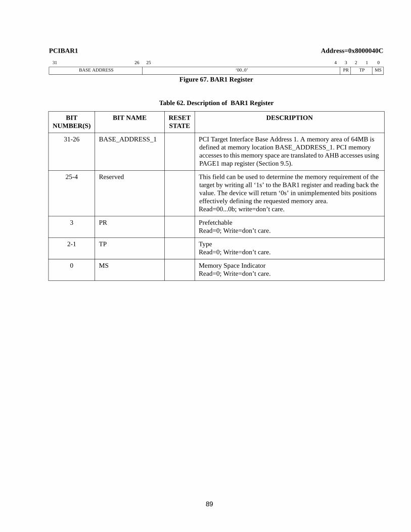
89
Table 62. Description of BAR1 Register
BIT NUMBER(S)
BIT NAME RESET STATE
DESCRIPTION
31-26 BASE_ADDRESS_1 PCI Target Interface Base Address 1. A memory area of 64MB is defined at memory location BASE_ADDRESS_1. PCI memory accesses to this memory space are translated to AHB accesses using PAGE1 map register (Section 9.5).
25-4 Reserved This field can be used to determine the memory requirement of the target by writing all ‘1s’ to the BAR1 register and reading back the value. The device will return ‘0s’ in unimplemented bits positions effectively defining the requested memory area.Read=00...0b; write=don’t care.
3 PR PrefetchableRead=0; Write=don’t care.
2-1 TP TypeRead=0; Write=don’t care.
0 MS Memory Space IndicatorRead=0; Write=don’t care.
PCIBAR1 Address=0x8000040C
31 26 25 4 3 2 1 0
BASE ADDRESS ‘00..0’ PR TP MS
Figure 67. BAR1 Register
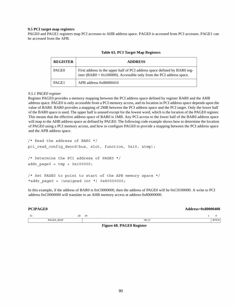
90
9.5 PCI target map registersPAGE0 and PAGE1 registers map PCI accesses to AHB address space. PAGE0 is accessed from PCI accesses. PAGE1 can be accessed from the APB.
9.5.1 PAGE0 registerRegister PAGE0 provides a memory mapping between the PCI address space defined by register BAR0 and the AHB address space. PAGE0 is only accessible from a PCI memory access, and its location in PCI address space depends upon the value of BAR0. BAR0 provides a mapping of 2MB between the PCI address space and the PCI target. Only the lower half of the BAR0 space is used. The upper half is unused except for the lowest word, which is the location of the PAGE0 register. This means that the effective address space of BAR0 is 1MB. Any PCI access to the lower half of the BAR0 address space will map to the AHB address space as defined by PAGE0. The following code example shows how to determine the location of PAGE0 using a PCI memory access, and how to configure PAGE0 to provide a mapping between the PCI address space and the APB address space.
/* Read the address of BAR0 */
pci_read_config_dword(bus, slot, function, 0x10, &tmp);
/* Determine the PCI address of PAGE0 */
addr_page0 = tmp + 0x100000;
/* Set PAGE0 to point to start of the APB memory space */
*addr_page0 = (unsigned int *) 0x80000000;
In this example, if the address of BAR0 is 0xC0000000, then the address of PAGE0 will be 0xC0100000. A write to PCI address 0xC0000000 will translate to an AHB memory access at address 0x80000000.
Table 63. PCI Target Map Registers
REGISTER ADDRESS
PAGE0 First address in the upper half of PCI address space defined by BAR0 reg-ister (BAR0 + 0x100000). Accessible only from the PCI address space.
PAGE1 APB address 0x80000410
PCIPAGE0 Address=0x80000408
31 20 19 1 0
PAGE0_MAP ‘00..0’ BTEN
Figure 68. PAGE0 Register
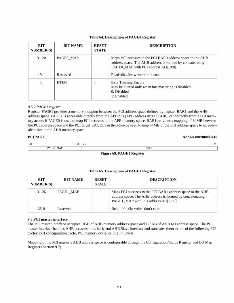
91
9.5.2 PAGE1 registerRegister PAGE1 provides a memory mapping between the PCI address space defined by register BAR1 and the AHB address space. PAGE1 is accessible directly from the APB bus (APB address 0x80000410), or indirectly from a PCI mem-ory access if PAGE0 is used to map PCI accesses to the APB memory space. BAR1 provides a mapping of 64MB between the PCI address space and the PCI target. PAGE1 can therefore be used to map 64MB of the PCI address space to an equiv-alent size in the AHB memory space.
9.6 PCI master interfaceThe PCI master interface occupies 1GB of AHB memory address space and 128 kB of AHB I/O address space. The PCI master interface handles AHB accesses to its back-end AHB Slave interface and translates them to one of the following PCI cycles: PCI configuration cycle, PCI memory cycle, or PCI I/O cycle.
Mapping of the PCI master’s AHB address space is configurable through the Configuration/Status Register and I/O Map Register (Section 9.7).
Table 64. Description of PAGE0 Register
BIT NUMBER(S)
BIT NAME RESET STATE
DESCRIPTION
31-20 PAGE0_MAP Maps PCI accesses to the PCI BAR0 address space to the AHB address space. The AHB address is formed by concatenating PAGE0_MAP with PCI address AD[19:0].
19-1 Reserved Read=00...0b; write=don’t care.
0 BTEN 1 Byte Twisting EnableMay be altered only when bus mastering is disabled.0: Disabled1: Enabled
Table 65. Description of PAGE1 Register
BIT NUMBER(S)
BIT NAME RESET STATE
DESCRIPTION
31-26 PAGE1_MAP Maps PCI accesses to the PCI BAR1 address space to the AHB address space. The AHB address is formed by concatenating PAGE1_MAP with PCI address AD[25:0].
25-0 Reserved Read=00...0b; write=don’t care.
PCIPAGE1 Address=0x80000410
31 26 25 0
PAGE1_MAP ‘00..0’
Figure 69. PAGE1 Register
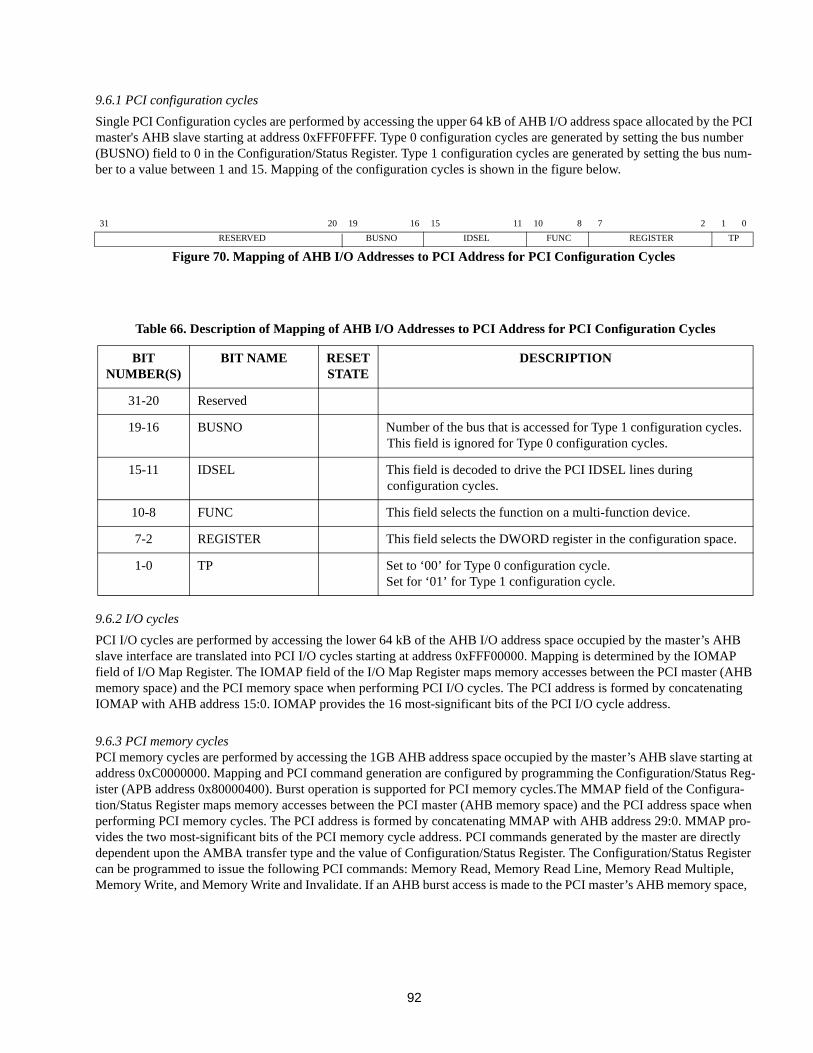
92
9.6.1 PCI configuration cycles
Single PCI Configuration cycles are performed by accessing the upper 64 kB of AHB I/O address space allocated by the PCI master's AHB slave starting at address 0xFFF0FFFF. Type 0 configuration cycles are generated by setting the bus number (BUSNO) field to 0 in the Configuration/Status Register. Type 1 configuration cycles are generated by setting the bus num-ber to a value between 1 and 15. Mapping of the configuration cycles is shown in the figure below.
9.6.2 I/O cycles
PCI I/O cycles are performed by accessing the lower 64 kB of the AHB I/O address space occupied by the master’s AHB slave interface are translated into PCI I/O cycles starting at address 0xFFF00000. Mapping is determined by the IOMAP field of I/O Map Register. The IOMAP field of the I/O Map Register maps memory accesses between the PCI master (AHB memory space) and the PCI memory space when performing PCI I/O cycles. The PCI address is formed by concatenating IOMAP with AHB address 15:0. IOMAP provides the 16 most-significant bits of the PCI I/O cycle address.
9.6.3 PCI memory cyclesPCI memory cycles are performed by accessing the 1GB AHB address space occupied by the master’s AHB slave starting at address 0xC0000000. Mapping and PCI command generation are configured by programming the Configuration/Status Reg-ister (APB address 0x80000400). Burst operation is supported for PCI memory cycles.The MMAP field of the Configura-tion/Status Register maps memory accesses between the PCI master (AHB memory space) and the PCI address space when performing PCI memory cycles. The PCI address is formed by concatenating MMAP with AHB address 29:0. MMAP pro-vides the two most-significant bits of the PCI memory cycle address. PCI commands generated by the master are directly dependent upon the AMBA transfer type and the value of Configuration/Status Register. The Configuration/Status Register can be programmed to issue the following PCI commands: Memory Read, Memory Read Line, Memory Read Multiple, Memory Write, and Memory Write and Invalidate. If an AHB burst access is made to the PCI master’s AHB memory space,
Table 66. Description of Mapping of AHB I/O Addresses to PCI Address for PCI Configuration Cycles
BIT NUMBER(S)
BIT NAME RESET STATE
DESCRIPTION
31-20 Reserved
19-16 BUSNO Number of the bus that is accessed for Type 1 configuration cycles. This field is ignored for Type 0 configuration cycles.
15-11 IDSEL This field is decoded to drive the PCI IDSEL lines during configuration cycles.
10-8 FUNC This field selects the function on a multi-function device.
7-2 REGISTER This field selects the DWORD register in the configuration space.
1-0 TP Set to ‘00’ for Type 0 configuration cycle.Set for ‘01’ for Type 1 configuration cycle.
31 20 19 16 15 11 10 8 7 2 1 0
RESERVED BUSNO IDSEL FUNC REGISTER TP
Figure 70. Mapping of AHB I/O Addresses to PCI Address for PCI Configuration Cycles
it is translated to burst PCI memory cycle. When the PCI master interface is busy performing the transaction on the PCI bus, its AHB slave interface will not be able to accept new requests. A ‘Retry’ response will be given to all accesses to its AHB slave interface. The requesting AHB master repeats its request until an ‘OK’ or ‘Error’ response is given by the PCI master’s AHB slave interface.
Note: ‘RETRY’ responses on the PCI bus are not transparent and will automatically be retried by the master PCI interface until the transfer is either finished or aborted. For burst accesses, only linear-incremental mode is supported and is directly translated from AMBA commands. Byte enables on the PCI bus are translated from the HSIZE control AHB signal and the AHB address according to the table below. Only WORD, HALF-WORD and BYTE values of HSIZE are valid.
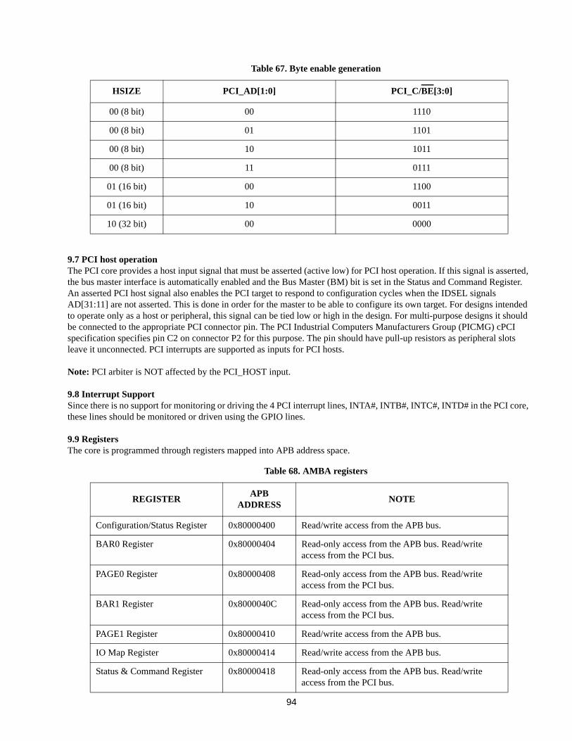
94
9.7 PCI host operationThe PCI core provides a host input signal that must be asserted (active low) for PCI host operation. If this signal is asserted, the bus master interface is automatically enabled and the Bus Master (BM) bit is set in the Status and Command Register. An asserted PCI host signal also enables the PCI target to respond to configuration cycles when the IDSEL signals AD[31:11] are not asserted. This is done in order for the master to be able to configure its own target. For designs intended to operate only as a host or peripheral, this signal can be tied low or high in the design. For multi-purpose designs it should be connected to the appropriate PCI connector pin. The PCI Industrial Computers Manufacturers Group (PICMG) cPCI specification specifies pin C2 on connector P2 for this purpose. The pin should have pull-up resistors as peripheral slots leave it unconnected. PCI interrupts are supported as inputs for PCI hosts.
Note: PCI arbiter is NOT affected by the PCI_HOST input.
9.8 Interrupt SupportSince there is no support for monitoring or driving the 4 PCI interrupt lines, INTA#, INTB#, INTC#, INTD# in the PCI core, these lines should be monitored or driven using the GPIO lines.
9.9 RegistersThe core is programmed through registers mapped into APB address space.
Table 67. Byte enable generation
HSIZE PCI_AD[1:0] PCI_C/BE[3:0]
00 (8 bit) 00 1110
00 (8 bit) 01 1101
00 (8 bit) 10 1011
00 (8 bit) 11 0111
01 (16 bit) 00 1100
01 (16 bit) 10 0011
10 (32 bit) 00 0000
Table 68. AMBA registers
REGISTERAPB
ADDRESSNOTE
Configuration/Status Register 0x80000400 Read/write access from the APB bus.
BAR0 Register 0x80000404 Read-only access from the APB bus. Read/write access from the PCI bus.
PAGE0 Register 0x80000408 Read-only access from the APB bus. Read/write access from the PCI bus.
BAR1 Register 0x8000040C Read-only access from the APB bus. Read/write access from the PCI bus.
PAGE1 Register 0x80000410 Read/write access from the APB bus.
IO Map Register 0x80000414 Read/write access from the APB bus.
Status & Command Register 0x80000418 Read-only access from the APB bus. Read/write access from the PCI bus.
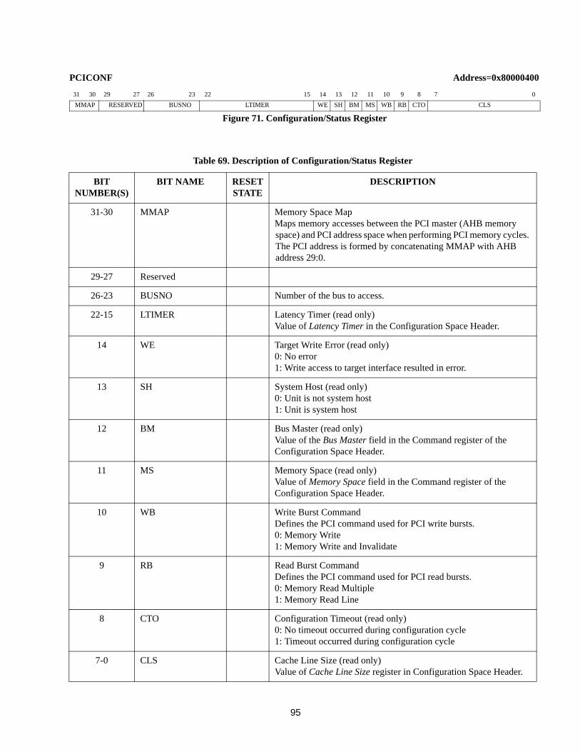
95
Table 69. Description of Configuration/Status Register
BIT NUMBER(S)
BIT NAME RESET STATE
DESCRIPTION
31-30 MMAP Memory Space MapMaps memory accesses between the PCI master (AHB memory space) and PCI address space when performing PCI memory cycles. The PCI address is formed by concatenating MMAP with AHB address 29:0.
29-27 Reserved
26-23 BUSNO Number of the bus to access.
22-15 LTIMER Latency Timer (read only)Value of Latency Timer in the Configuration Space Header.
14 WE Target Write Error (read only)0: No error1: Write access to target interface resulted in error.
13 SH System Host (read only)0: Unit is not system host1: Unit is system host
12 BM Bus Master (read only)Value of the Bus Master field in the Command register of the Configuration Space Header.
11 MS Memory Space (read only)Value of Memory Space field in the Command register of the Configuration Space Header.
10 WB Write Burst CommandDefines the PCI command used for PCI write bursts.0: Memory Write1: Memory Write and Invalidate
9 RB Read Burst CommandDefines the PCI command used for PCI read bursts.0: Memory Read Multiple1: Memory Read Line
8 CTO Configuration Timeout (read only)0: No timeout occurred during configuration cycle1: Timeout occurred during configuration cycle
7-0 CLS Cache Line Size (read only)Value of Cache Line Size register in Configuration Space Header.
PCICONF Address=0x80000400
31 30 29 27 26 23 22 15 14 13 12 11 10 9 8 7 0
MMAP RESERVED BUSNO LTIMER WE SH BM MS WB RB CTO CLS
Figure 71. Configuration/Status Register
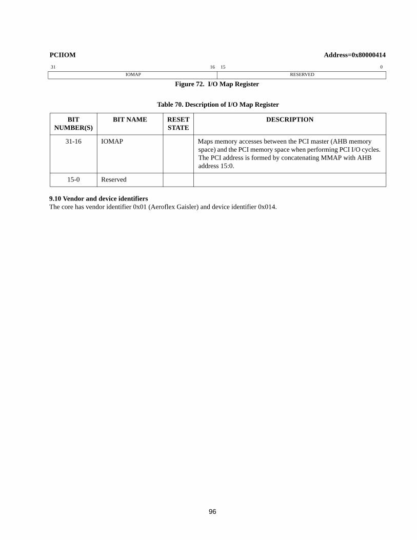
96
9.10 Vendor and device identifiersThe core has vendor identifier 0x01 (Aeroflex Gaisler) and device identifier 0x014.
Table 70. Description of I/O Map Register
BIT NUMBER(S)
BIT NAME RESET STATE
DESCRIPTION
31-16 IOMAP Maps memory accesses between the PCI master (AHB memory space) and the PCI memory space when performing PCI I/O cycles. The PCI address is formed by concatenating MMAP with AHB address 15:0.
15-0 Reserved
PCIIOM Address=0x80000414
31 16 15 0
IOMAP RESERVED
Figure 72. I/O Map Register
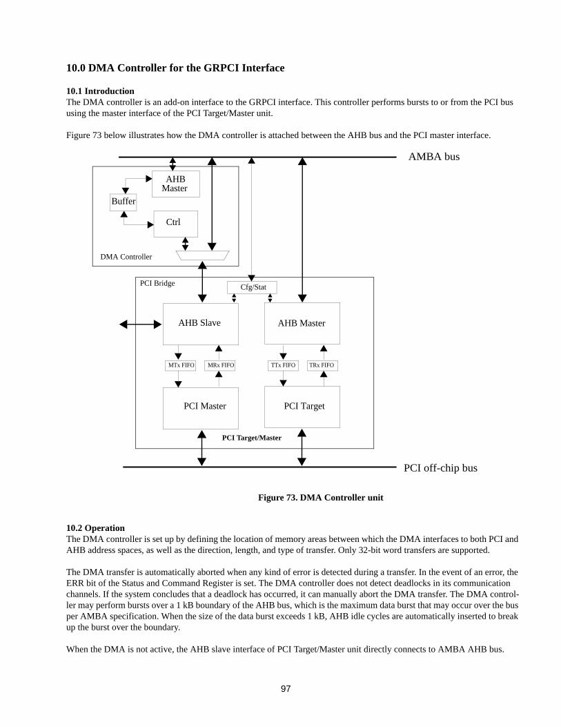
97
10.0 DMA Controller for the GRPCI Interface
10.1 IntroductionThe DMA controller is an add-on interface to the GRPCI interface. This controller performs bursts to or from the PCI bus using the master interface of the PCI Target/Master unit.
Figure 73 below illustrates how the DMA controller is attached between the AHB bus and the PCI master interface.
10.2 OperationThe DMA controller is set up by defining the location of memory areas between which the DMA interfaces to both PCI and AHB address spaces, as well as the direction, length, and type of transfer. Only 32-bit word transfers are supported.
The DMA transfer is automatically aborted when any kind of error is detected during a transfer. In the event of an error, the ERR bit of the Status and Command Register is set. The DMA controller does not detect deadlocks in its communication channels. If the system concludes that a deadlock has occurred, it can manually abort the DMA transfer. The DMA control-ler may perform bursts over a 1 kB boundary of the AHB bus, which is the maximum data burst that may occur over the bus per AMBA specification. When the size of the data burst exceeds 1 kB, AHB idle cycles are automatically inserted to break up the burst over the boundary.
When the DMA is not active, the AHB slave interface of PCI Target/Master unit directly connects to AMBA AHB bus.
Figure 73. DMA Controller unit
PCI Master PCI Target
AHB Slave AHB Master
Cfg/Stat
AMBA bus
PCI off-chip bus
PCI Bridge
MTx FIFO MRx FIFO TTx FIFO TRx FIFO
AHB
Ctrl
BufferMaster
DMA Controller
PCI Target/Master
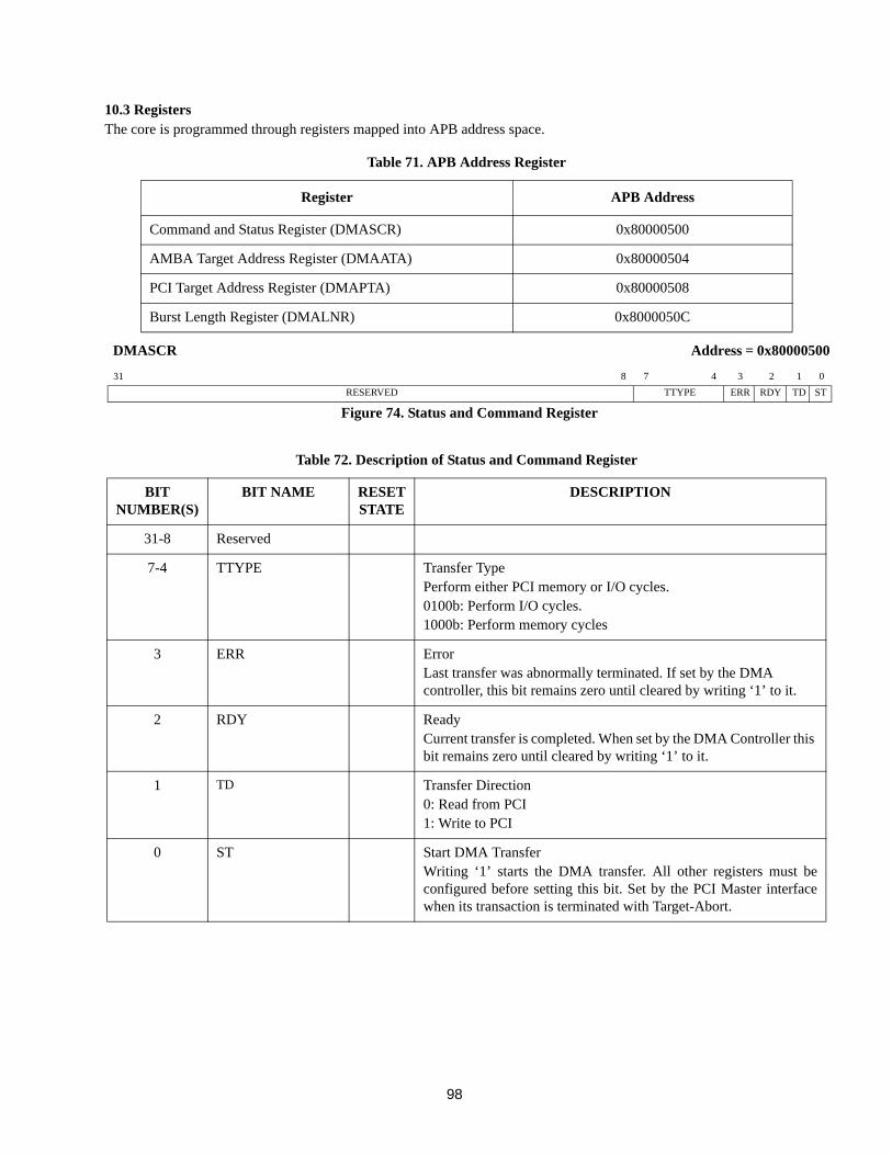
98
10.3 RegistersThe core is programmed through registers mapped into APB address space.
Table 71. APB Address Register
Register APB Address
Command and Status Register (DMASCR) 0x80000500
AMBA Target Address Register (DMAATA) 0x80000504
PCI Target Address Register (DMAPTA) 0x80000508
Burst Length Register (DMALNR) 0x8000050C
Table 72. Description of Status and Command Register
BIT NUMBER(S)
BIT NAME RESET STATE
DESCRIPTION
31-8 Reserved
7-4 TTYPE Transfer TypePerform either PCI memory or I/O cycles.0100b: Perform I/O cycles.1000b: Perform memory cycles
3 ERR ErrorLast transfer was abnormally terminated. If set by the DMA controller, this bit remains zero until cleared by writing ‘1’ to it.
2 RDY ReadyCurrent transfer is completed. When set by the DMA Controller this bit remains zero until cleared by writing ‘1’ to it.
1 TD Transfer Direction0: Read from PCI1: Write to PCI
0 ST Start DMA TransferWriting ‘1’ starts the DMA transfer. All other registers must beconfigured before setting this bit. Set by the PCI Master interfacewhen its transaction is terminated with Target-Abort.
DMASCR Address = 0x80000500
31 8 7 4 3 2 1 0
RESERVED TTYPE ERR RDY TD ST
Figure 74. Status and Command Register
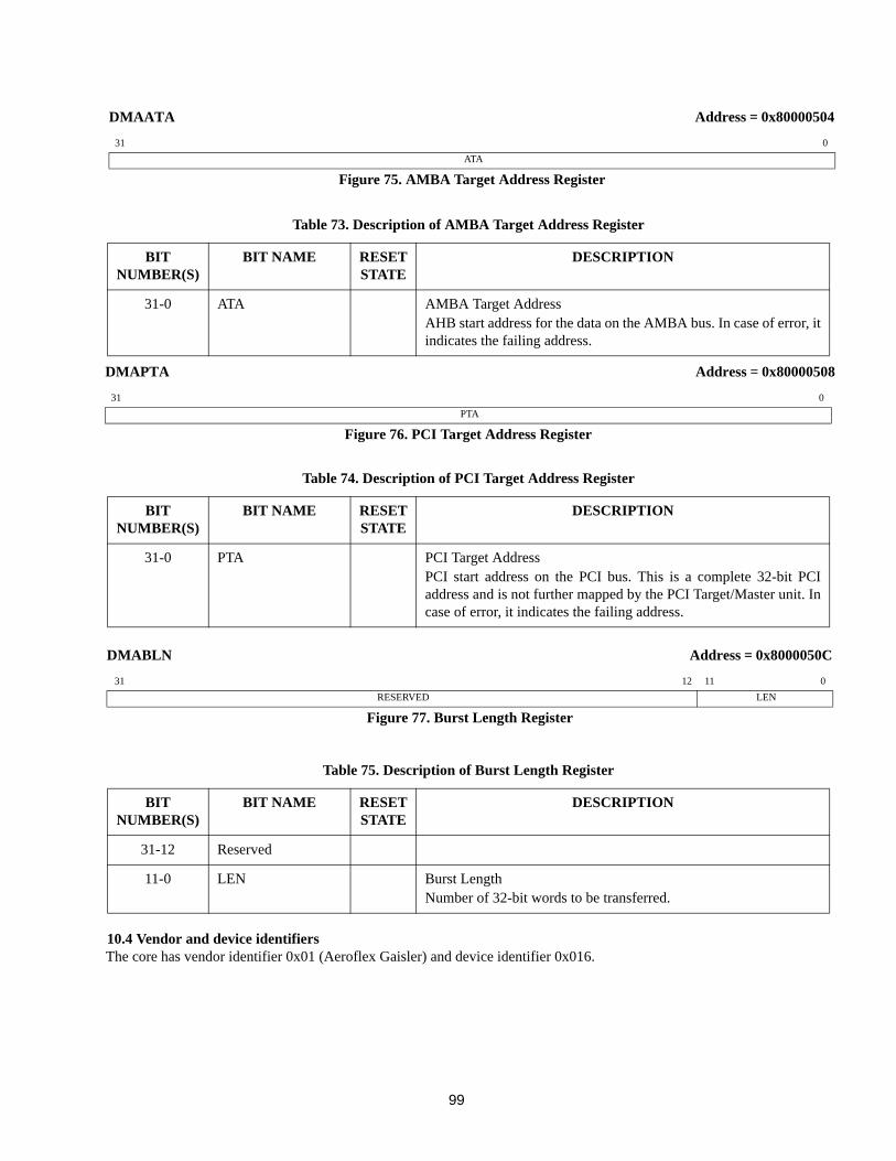
99
10.4 Vendor and device identifiersThe core has vendor identifier 0x01 (Aeroflex Gaisler) and device identifier 0x016.
Table 73. Description of AMBA Target Address Register
BIT NUMBER(S)
BIT NAME RESET STATE
DESCRIPTION
31-0 ATA AMBA Target AddressAHB start address for the data on the AMBA bus. In case of error, itindicates the failing address.
Table 74. Description of PCI Target Address Register
BIT NUMBER(S)
BIT NAME RESET STATE
DESCRIPTION
31-0 PTA PCI Target AddressPCI start address on the PCI bus. This is a complete 32-bit PCIaddress and is not further mapped by the PCI Target/Master unit. Incase of error, it indicates the failing address.
Table 75. Description of Burst Length Register
BIT NUMBER(S)
BIT NAME RESET STATE
DESCRIPTION
31-12 Reserved
11-0 LEN Burst LengthNumber of 32-bit words to be transferred.
DMAPTA Address = 0x80000508
31 0
PTA
Figure 76. PCI Target Address Register
DMABLN Address = 0x8000050C
31 12 11 0
RESERVED LEN
Figure 77. Burst Length Register
DMAATA Address = 0x80000504
31 0
ATA
Figure 75. AMBA Target Address Register
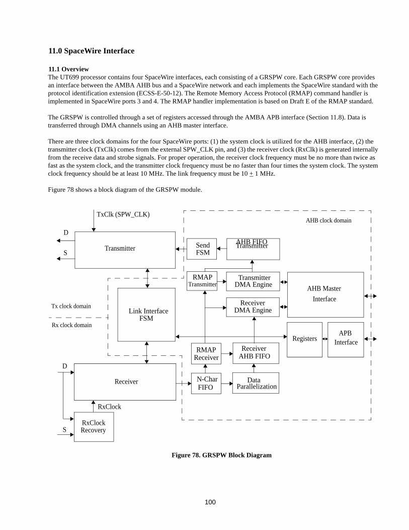
100
11.0 SpaceWire Interface
11.1 OverviewThe UT699 processor contains four SpaceWire interfaces, each consisting of a GRSPW core. Each GRSPW core provides an interface between the AMBA AHB bus and a SpaceWire network and each implements the SpaceWire standard with the protocol identification extension (ECSS-E-50-12). The Remote Memory Access Protocol (RMAP) command handler is implemented in SpaceWire ports 3 and 4. The RMAP handler implementation is based on Draft E of the RMAP standard.
The GRSPW is controlled through a set of registers accessed through the AMBA APB interface (Section 11.8). Data is transferred through DMA channels using an AHB master interface.
There are three clock domains for the four SpaceWire ports: (1) the system clock is utilized for the AHB interface, (2) the transmitter clock (TxClk) comes from the external SPW_CLK pin, and (3) the receiver clock (RxClk) is generated internally from the receive data and strobe signals. For proper operation, the receiver clock frequency must be no more than twice as fast as the system clock, and the transmitter clock frequency must be no faster than four times the system clock. The system clock frequency should be at least 10 MHz. The link frequency must be 10 + 1 MHz.
Figure 78 shows a block diagram of the GRSPW module.
Transmitter
Receiver
D
S
S
D
RxClockRecovery
TxClk (SPW_CLK)
RxClock
AHB Master
Interface
Transmitter
N-CharFIFO
Link InterfaceFSM
AHB clock domain
Tx clock domain
Rx clock domain
Data Parallelization
Receiver AHB FIFO
TransmitterDMA Engine
RegistersAPB
Interface
ReceiverDMA Engine
SendFSM
RMAPReceiver
RMAPTransmitter
Figure 78. GRSPW Block Diagram
AHB FIFO
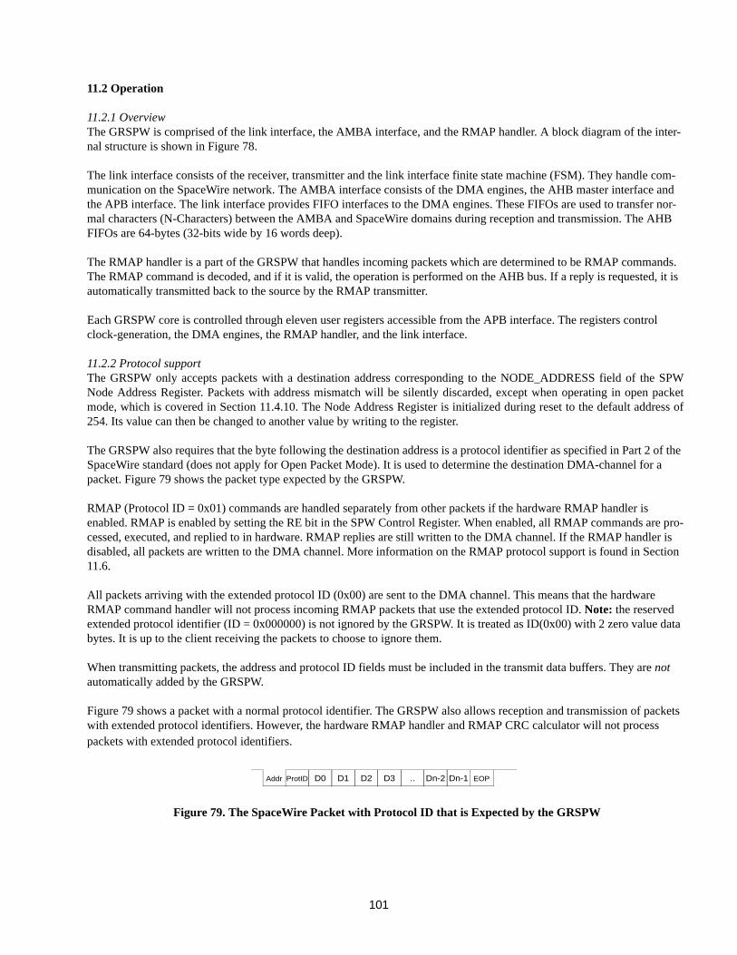
101
11.2 Operation
11.2.1 OverviewThe GRSPW is comprised of the link interface, the AMBA interface, and the RMAP handler. A block diagram of the inter-nal structure is shown in Figure 78.
The link interface consists of the receiver, transmitter and the link interface finite state machine (FSM). They handle com-munication on the SpaceWire network. The AMBA interface consists of the DMA engines, the AHB master interface and the APB interface. The link interface provides FIFO interfaces to the DMA engines. These FIFOs are used to transfer nor-mal characters (N-Characters) between the AMBA and SpaceWire domains during reception and transmission. The AHB FIFOs are 64-bytes (32-bits wide by 16 words deep).
The RMAP handler is a part of the GRSPW that handles incoming packets which are determined to be RMAP commands. The RMAP command is decoded, and if it is valid, the operation is performed on the AHB bus. If a reply is requested, it is automatically transmitted back to the source by the RMAP transmitter.
Each GRSPW core is controlled through eleven user registers accessible from the APB interface. The registers control clock-generation, the DMA engines, the RMAP handler, and the link interface.
11.2.2 Protocol supportThe GRSPW only accepts packets with a destination address corresponding to the NODE_ADDRESS field of the SPWNode Address Register. Packets with address mismatch will be silently discarded, except when operating in open packetmode, which is covered in Section 11.4.10. The Node Address Register is initialized during reset to the default address of254. Its value can then be changed to another value by writing to the register.
The GRSPW also requires that the byte following the destination address is a protocol identifier as specified in Part 2 of the SpaceWire standard (does not apply for Open Packet Mode). It is used to determine the destination DMA-channel for a packet. Figure 79 shows the packet type expected by the GRSPW.
RMAP (Protocol ID = 0x01) commands are handled separately from other packets if the hardware RMAP handler is enabled. RMAP is enabled by setting the RE bit in the SPW Control Register. When enabled, all RMAP commands are pro-cessed, executed, and replied to in hardware. RMAP replies are still written to the DMA channel. If the RMAP handler is disabled, all packets are written to the DMA channel. More information on the RMAP protocol support is found in Section 11.6.
All packets arriving with the extended protocol ID (0x00) are sent to the DMA channel. This means that the hardware RMAP command handler will not process incoming RMAP packets that use the extended protocol ID. Note: the reserved extended protocol identifier (ID = 0x000000) is not ignored by the GRSPW. It is treated as ID(0x00) with 2 zero value data bytes. It is up to the client receiving the packets to choose to ignore them.
When transmitting packets, the address and protocol ID fields must be included in the transmit data buffers. They are not automatically added by the GRSPW.
Figure 79 shows a packet with a normal protocol identifier. The GRSPW also allows reception and transmission of packets with extended protocol identifiers. However, the hardware RMAP handler and RMAP CRC calculator will not process packets with extended protocol identifiers.
Addr ProtID Dn-2..D3D2D1D0 Dn-1 EOP
Figure 79. The SpaceWire Packet with Protocol ID that is Expected by the GRSPW

102
11.3 Link interfaceThe link interface handles the communication on the SpaceWire network and consists of the transmitter, receiver, a finite state machine (FSM), and FIFO interfaces. An overview of the architecture is found in Figure 80.
11.3.1 Link interface FSMThe FSM controls the link interface (a more detailed description is found in the SpaceWire standard). The low-level protocol handling (the signal and character level of the SpaceWire standard) is handled by the transmitter and receiver, while the FSM in the host domain handles the exchange level.
The link interface FSM is controlled through the SPW Control Register. The link can be disabled through the Link Disable (LD) bit, which depending on the current state, either prevents the link interface from reaching the started state, or forces it to the error-reset state. When the link is enabled, the link interface FSM is allowed to enter the started state when either the link start (LS) bit is set, or when a NULL character has been received with the Autostart (AS) bit set.
The current state of the link interface determines which type of characters are allowed to be transmitted. Together with the requests made from the host interfaces, the current state determine what character will be sent. The current state can be determined by reading the Link State (LS) field of the SPW Status Register.
Time codes are sent when the FSM is in the run-state and a request is made through the time interface. This is described in section 11.3.4.
When the link interface is in either the connecting- or run-state, it is allowed to send link Characters (L-Char). L-Char’s are sent automatically by the link interface when possible. This is done based on the maximum value of 56 for the outstanding credit counter and the currently free space in the receiver N-Char FIFO. FCTs are sent as long as the outstanding counter is less than or equal to 48 and there are at least 8 more empty FIFO entries than the counter value.
N-Chars are sent in the run-state when they are available from the transmitter FIFO and there are credits available. NULLs are sent when no other character transmission is requested or when the FSM is in a state that does not allow any transmis-sions to occur.
The credit counter (incoming credits) is automatically increased when FCTs are received and decreased when N-Chars are transmitted. Received N-Chars are stored to the receiver N-Char FIFO for further handling by the DMA interface. Received time-codes are handled by the time-interface.
11.3.2 TransmitterThe state of the FSM, credit counters, requests from the time-interface and requests from the DMA-interface are used to determine the next character to be transmitted. The type of character and the character itself (for N-Chars and time-codes) to be transmitted are presented to the low-level transmitter which is located in the TxClk clock domain.
The separate clock domains allow the SpaceWire link to run on a different frequency than the host system clock. The UT699 has a separate clock input which is used to generate the transmitter clock. Since the transmitter often runs at frequencies greater than 100MHz, as much logic as possible has been placed in the slower system clock domain to minimize power con-sumption and timing issues.
The transmitter logic in the host clock domain decides what character to send next, sets the proper control signal, and pres-ents any required characters to the low-level transmitter as shown in Figure 80. The transmitter handles sends the requested characters and generates parity and control bits as needed. If no requests are made from the host domain, NULLs are sent as long as the transmitter is enabled. Most of the signal and character levels of the SpaceWire standard are handled in the trans-mitter.
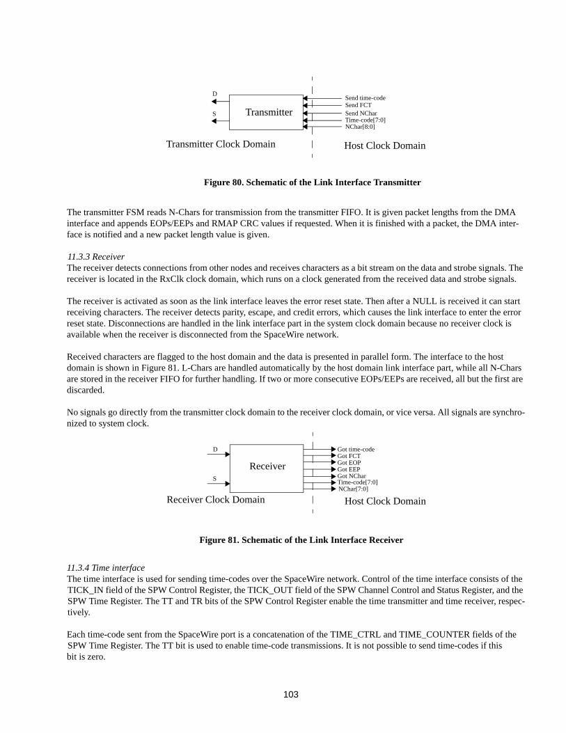
103
The transmitter FSM reads N-Chars for transmission from the transmitter FIFO. It is given packet lengths from the DMA interface and appends EOPs/EEPs and RMAP CRC values if requested. When it is finished with a packet, the DMA inter-face is notified and a new packet length value is given.
11.3.3 ReceiverThe receiver detects connections from other nodes and receives characters as a bit stream on the data and strobe signals. The receiver is located in the RxClk clock domain, which runs on a clock generated from the received data and strobe signals.
The receiver is activated as soon as the link interface leaves the error reset state. Then after a NULL is received it can start receiving characters. The receiver detects parity, escape, and credit errors, which causes the link interface to enter the error reset state. Disconnections are handled in the link interface part in the system clock domain because no receiver clock is available when the receiver is disconnected from the SpaceWire network.
Received characters are flagged to the host domain and the data is presented in parallel form. The interface to the host domain is shown in Figure 81. L-Chars are handled automatically by the host domain link interface part, while all N-Chars are stored in the receiver FIFO for further handling. If two or more consecutive EOPs/EEPs are received, all but the first are discarded.
No signals go directly from the transmitter clock domain to the receiver clock domain, or vice versa. All signals are synchro-nized to system clock.
11.3.4 Time interfaceThe time interface is used for sending time-codes over the SpaceWire network. Control of the time interface consists of the TICK_IN field of the SPW Control Register, the TICK_OUT field of the SPW Channel Control and Status Register, and the SPW Time Register. The TT and TR bits of the SPW Control Register enable the time transmitter and time receiver, respec-tively.
Each time-code sent from the SpaceWire port is a concatenation of the TIME_CTRL and TIME_COUNTER fields of the SPW Time Register. The TT bit is used to enable time-code transmissions. It is not possible to send time-codes if thisbit is zero.
Transmitter Clock Domain Host Clock Domain
Transmitter
D
S
Send time-codeSend FCTSend NCharTime-code[7:0]NChar[8:0]
Figure 80. Schematic of the Link Interface Transmitter
Receiver Clock Domain Host Clock Domain
Receiver
D
S
Got time-codeGot FCT
Got NCharTime-code[7:0]NChar[7:0]
Got EEPGot EOP
Figure 81. Schematic of the Link Interface Receiver
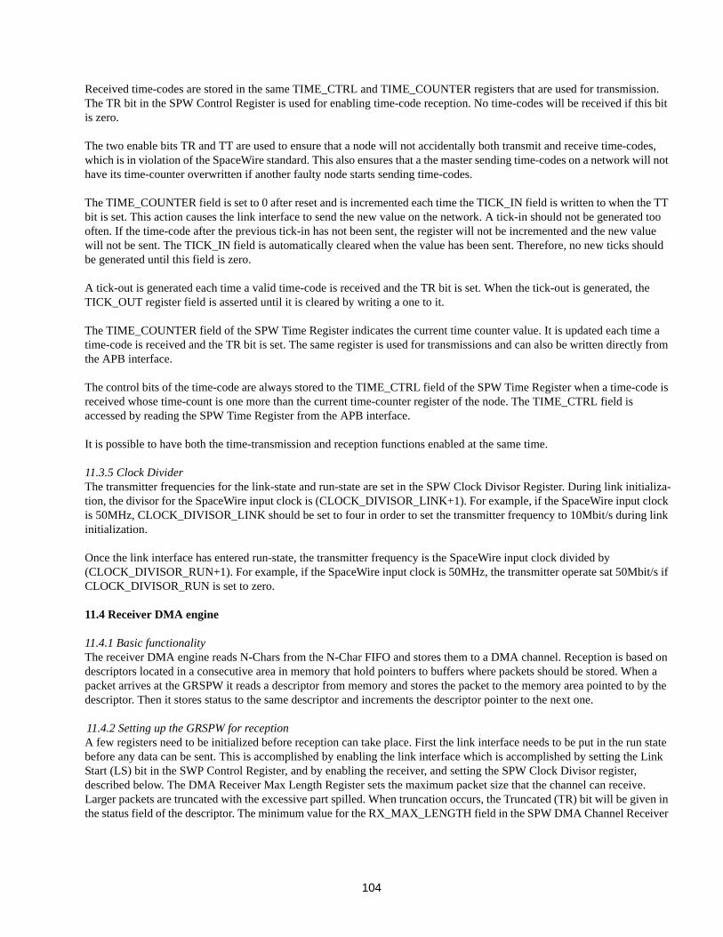
104
Received time-codes are stored in the same TIME_CTRL and TIME_COUNTER registers that are used for transmission. The TR bit in the SPW Control Register is used for enabling time-code reception. No time-codes will be received if this bit is zero.
The two enable bits TR and TT are used to ensure that a node will not accidentally both transmit and receive time-codes, which is in violation of the SpaceWire standard. This also ensures that a the master sending time-codes on a network will not have its time-counter overwritten if another faulty node starts sending time-codes.
The TIME_COUNTER field is set to 0 after reset and is incremented each time the TICK_IN field is written to when the TT bit is set. This action causes the link interface to send the new value on the network. A tick-in should not be generated too often. If the time-code after the previous tick-in has not been sent, the register will not be incremented and the new value will not be sent. The TICK_IN field is automatically cleared when the value has been sent. Therefore, no new ticks should be generated until this field is zero.
A tick-out is generated each time a valid time-code is received and the TR bit is set. When the tick-out is generated, the TICK_OUT register field is asserted until it is cleared by writing a one to it.
The TIME_COUNTER field of the SPW Time Register indicates the current time counter value. It is updated each time a time-code is received and the TR bit is set. The same register is used for transmissions and can also be written directly from the APB interface.
The control bits of the time-code are always stored to the TIME_CTRL field of the SPW Time Register when a time-code is received whose time-count is one more than the current time-counter register of the node. The TIME_CTRL field is accessed by reading the SPW Time Register from the APB interface.
It is possible to have both the time-transmission and reception functions enabled at the same time.
11.3.5 Clock DividerThe transmitter frequencies for the link-state and run-state are set in the SPW Clock Divisor Register. During link initializa-tion, the divisor for the SpaceWire input clock is (CLOCK_DIVISOR_LINK+1). For example, if the SpaceWire input clock is 50MHz, CLOCK_DIVISOR_LINK should be set to four in order to set the transmitter frequency to 10Mbit/s during link initialization.
Once the link interface has entered run-state, the transmitter frequency is the SpaceWire input clock divided by (CLOCK_DIVISOR_RUN+1). For example, if the SpaceWire input clock is 50MHz, the transmitter operate sat 50Mbit/s if CLOCK_DIVISOR_RUN is set to zero.
11.4 Receiver DMA engine
11.4.1 Basic functionalityThe receiver DMA engine reads N-Chars from the N-Char FIFO and stores them to a DMA channel. Reception is based on descriptors located in a consecutive area in memory that hold pointers to buffers where packets should be stored. When a packet arrives at the GRSPW it reads a descriptor from memory and stores the packet to the memory area pointed to by the descriptor. Then it stores status to the same descriptor and increments the descriptor pointer to the next one.
11.4.2 Setting up the GRSPW for receptionA few registers need to be initialized before reception can take place. First the link interface needs to be put in the run state before any data can be sent. This is accomplished by enabling the link interface which is accomplished by setting the Link Start (LS) bit in the SWP Control Register, and by enabling the receiver, and setting the SPW Clock Divisor register, described below. The DMA Receiver Max Length Register sets the maximum packet size that the channel can receive. Larger packets are truncated with the excessive part spilled. When truncation occurs, the Truncated (TR) bit will be given in the status field of the descriptor. The minimum value for the RX_MAX_LENGTH field in the SPW DMA Channel Receiver
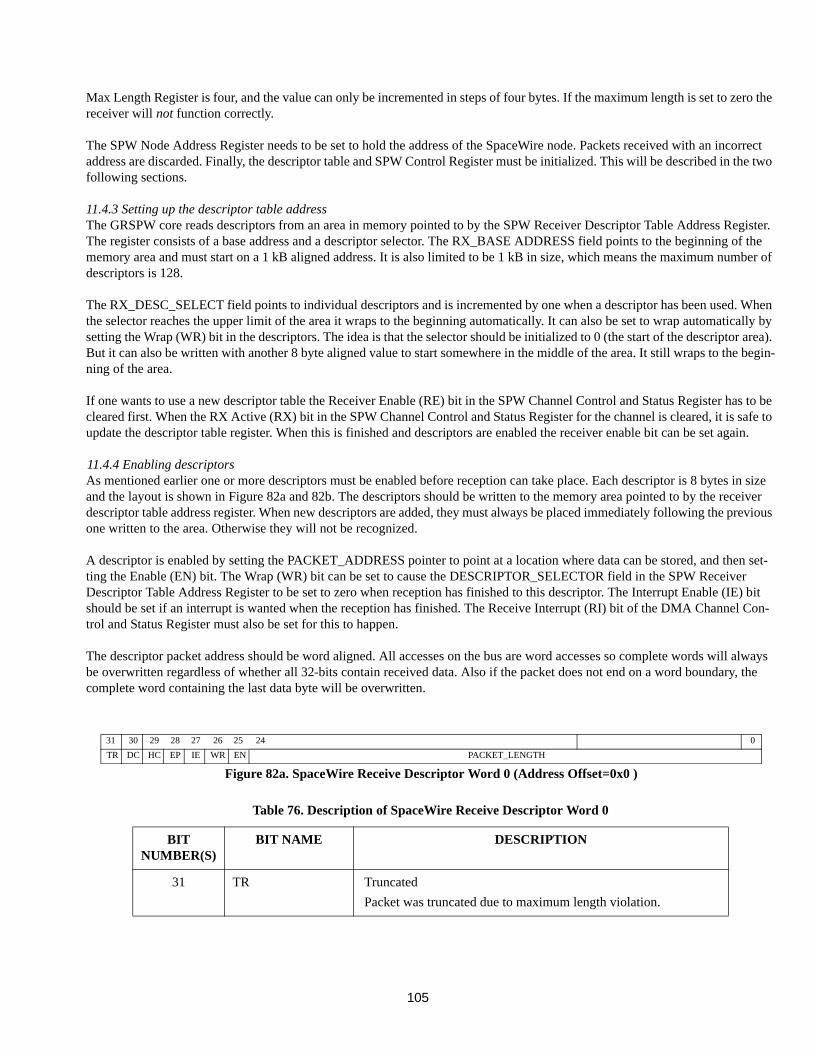
105
Max Length Register is four, and the value can only be incremented in steps of four bytes. If the maximum length is set to zero the receiver will not function correctly.
The SPW Node Address Register needs to be set to hold the address of the SpaceWire node. Packets received with an incorrect address are discarded. Finally, the descriptor table and SPW Control Register must be initialized. This will be described in the two following sections.
11.4.3 Setting up the descriptor table addressThe GRSPW core reads descriptors from an area in memory pointed to by the SPW Receiver Descriptor Table Address Register. The register consists of a base address and a descriptor selector. The RX_BASE ADDRESS field points to the beginning of the memory area and must start on a 1 kB aligned address. It is also limited to be 1 kB in size, which means the maximum number of descriptors is 128.
The RX_DESC_SELECT field points to individual descriptors and is incremented by one when a descriptor has been used. When the selector reaches the upper limit of the area it wraps to the beginning automatically. It can also be set to wrap automatically by setting the Wrap (WR) bit in the descriptors. The idea is that the selector should be initialized to 0 (the start of the descriptor area). But it can also be written with another 8 byte aligned value to start somewhere in the middle of the area. It still wraps to the begin-ning of the area.
If one wants to use a new descriptor table the Receiver Enable (RE) bit in the SPW Channel Control and Status Register has to be cleared first. When the RX Active (RX) bit in the SPW Channel Control and Status Register for the channel is cleared, it is safe to update the descriptor table register. When this is finished and descriptors are enabled the receiver enable bit can be set again.
11.4.4 Enabling descriptorsAs mentioned earlier one or more descriptors must be enabled before reception can take place. Each descriptor is 8 bytes in size and the layout is shown in Figure 82a and 82b. The descriptors should be written to the memory area pointed to by the receiver descriptor table address register. When new descriptors are added, they must always be placed immediately following the previous one written to the area. Otherwise they will not be recognized.
A descriptor is enabled by setting the PACKET_ADDRESS pointer to point at a location where data can be stored, and then set-ting the Enable (EN) bit. The Wrap (WR) bit can be set to cause the DESCRIPTOR_SELECTOR field in the SPW Receiver Descriptor Table Address Register to be set to zero when reception has finished to this descriptor. The Interrupt Enable (IE) bit should be set if an interrupt is wanted when the reception has finished. The Receive Interrupt (RI) bit of the DMA Channel Con-trol and Status Register must also be set for this to happen.
The descriptor packet address should be word aligned. All accesses on the bus are word accesses so complete words will always be overwritten regardless of whether all 32-bits contain received data. Also if the packet does not end on a word boundary, the complete word containing the last data byte will be overwritten.
Table 76. Description of SpaceWire Receive Descriptor Word 0
BIT NUMBER(S)
BIT NAME DESCRIPTION
31 TR Truncated
Packet was truncated due to maximum length violation.
31 30 29 28 27 26 25 24 0
TR DC HC EP IE WR EN PACKET_LENGTH
Figure 82a. SpaceWire Receive Descriptor Word 0 (Address Offset=0x0 )
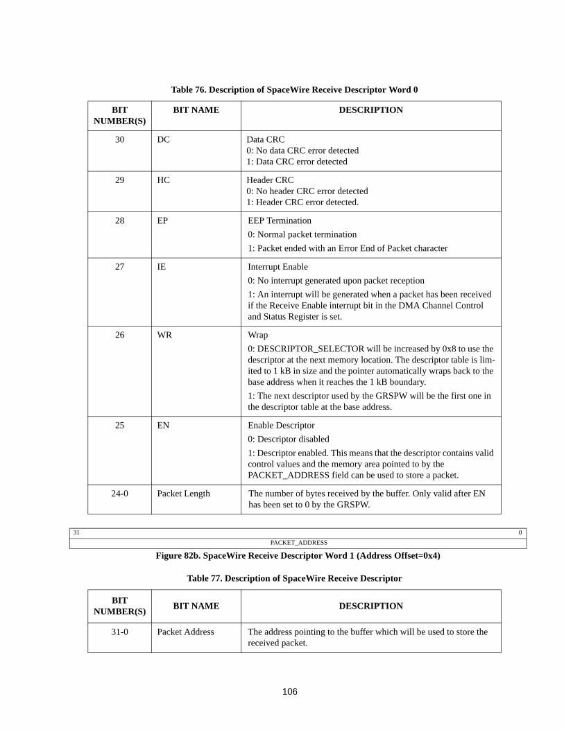
106
Table 76. Description of SpaceWire Receive Descriptor Word 0
BIT NUMBER(S)
BIT NAME DESCRIPTION
30 DC Data CRC0: No data CRC error detected1: Data CRC error detected
29 HC Header CRC0: No header CRC error detected1: Header CRC error detected.
28 EP EEP Termination
0: Normal packet termination
1: Packet ended with an Error End of Packet character
27 IE Interrupt Enable
0: No interrupt generated upon packet reception
1: An interrupt will be generated when a packet has been received if the Receive Enable interrupt bit in the DMA Channel Control and Status Register is set.
26 WR Wrap
0: DESCRIPTOR_SELECTOR will be increased by 0x8 to use the descriptor at the next memory location. The descriptor table is lim-ited to 1 kB in size and the pointer automatically wraps back to the base address when it reaches the 1 kB boundary.
1: The next descriptor used by the GRSPW will be the first one in the descriptor table at the base address.
25 EN Enable Descriptor
0: Descriptor disabled
1: Descriptor enabled. This means that the descriptor contains valid control values and the memory area pointed to by the PACKET_ADDRESS field can be used to store a packet.
24-0 Packet Length The number of bytes received by the buffer. Only valid after EN has been set to 0 by the GRSPW.
Table 77. Description of SpaceWire Receive Descriptor
BIT NUMBER(S)
BIT NAME DESCRIPTION
31-0 Packet Address The address pointing to the buffer which will be used to store the received packet.
31 0
PACKET_ADDRESS
Figure 82b. SpaceWire Receive Descriptor Word 1 (Address Offset=0x4)
107
11.4.5 Setting up the DMA control registerThe final step to receive packets is to set the control register in the following steps: The receiver must be enabled by setting the Receiver Enable (RE) bit in the SPW DMA Channel Control and Status Register. This can be done anytime; before this bit is set, no receiver operation will occur. The Receiver Descriptors Available (RD) bit in the DMA Control Register is then set to indicate that there are new active descriptors. This must always be done after the descriptors have been enabled or the GRSPW might not notice the new descriptors. More descriptors can be activated when reception has already started by enabling the descriptors and setting the RD bit. When these bits are set, reception starts immediately as soon as data arrives.
11.4.6 The effect to the control bits during receptionWhen the receiver is disabled all packets going to the DMA-channel are discarded. If the receiver is enabled the next state is entered where the RD bit is checked. This bit indicates whether there are active descriptors or not and should be set by the external application using the DMA channel each time descriptors are enabled as mentioned above. If the RD is ‘0’ and the No Spill (NS) bit is 0, the packets will be discarded. If NS is ‘1’, the GRSPW core waits until RD is set and then stores the received data. When RD is set the next descriptor is read and if enabled, the packet is received to the buffer. If the read descriptor is not enabled, i.e. the EN bit in the descriptor is 0, RD is set to ‘0’ and the packet is spilled depending on the value of NS.
The receiver can be disabled at any time and causes all packets received afterwards to be discarded. If a packet is currently being received when the receiver is disabled, the reception will finish normally. The RD bit can also be cleared at any time. It will not affect any ongoing receptions, but no more descriptors will be read until it is set again. RD is also cleared by the GRSPW when it reads a disabled descriptor as discussed above.
11.4.7 Address recognition and packet handlingWhen the receiver N-Char FIFO is not empty, N-Chars are read by the receiver DMA engine. The first character is inter-preted as the logical address, which is compared to the node address register. If it does not match, the complete packet is dis-carded (up to and including the next EOP/EEP). Otherwise, the next action taken depends on whether the node is configured with RMAP or not. If RMAP is disabled all packets are stored to the DMA channel, and depending on the conditions men-tioned in the previous section, the packet will be received or not. If the packet is received, complete packet including address and protocol ID, but excluding EOP/EEP, is stored to the address indicated in the descriptor. Otherwise, the complete packet is discarded.
If RMAP is enabled, the Protocol Identifier and Packet Type / Command / Source Path Address Length bytes in the received packet are first checked before any decisions are made. If the incoming packet is a RMAP packet (ID = 0x01) and the Com-mand field is 01b, the packet is processed by the RMAP command handler which is described in Section 11.6. Otherwise, the packet is processed by the DMA engine as when RMAP is disabled.
At least 2 non-EOP/EEP N-Chars need to be received for a packet to be stored to the DMA channel. If it is an RMAP packet with hardware RMAP enabled, 3 N-Chars are needed since the Command field of the Packet Type / Command / Source Path Address Length byte determines where the packet is processed. Packets smaller than these sizes are discarded.
11.4.8 Status bitsWhen the reception of a packet is finished, the enable (EN) bit in the current descriptor is set to ‘0’. When EN is ‘0’, the sta-tus bits are also valid as are the number of received bytes indicated in the PACKET_LENGTH field. The Packet Received (PR) bit in the SPW DMA Channel Control and Status Register is set each time a packet has been received. The GRSPW can also be made to generate an interrupt for this event if the Receive Interrupt (RI) bit is set.
CRC is always checked for all RMAP packets. If the received packet is not of RMAP type, the CRC error indication bits in the descriptor should be ignored. If the received packet is of RMAP type, the bits are valid and the Header CRC (HC) bit is set if a header CRC error was detected. In this case, the data CRC will not be calculated and the Data CRC (DC) bit is unde-fined. If the header CRC was correct, the DC bit will also contain a valid value and is set to ‘1’ if a data CRC error was detected.
108
11.4.9 Error handlingIf a packet reception needs to be aborted because of congestion on the network, the suggested solution is to set the Link Dis-able (LD) bit in the SPW Control Register to ‘1’. Unfortunately, this will also cause the packet currently being transmitted to be truncated, but this is the only safe solution since packet reception is a passive operation depending on the transmitter at the other end. A channel reset bit could be provided, but is not a satisfactory solution since the untransmitted characters would still be in the transmitter node. The next character (somewhere in the middle of the packet) would be interpreted as the node address which would probably cause the packet to be discarded, but not with 100% certainty. Usually this action is performed when a reception is stuck because of the transmitter not providing additional data. The channel reset would not resolve this congestion.
If an AHB error occurs during reception, the current packet is spilled up to and including the next EEP/EOP. The currently active channel is disabled and the receiver enters the idle state. The Link Disable (LD) bit in the SPW Control Register and the Link State (LS) bit in the SPW Status Register indicate this condition.
11.4.10 Open Packet modeThe GRSPW supports an open packet mode where all the data received is stored to the DMA channel regardless of the node address and possible early EOPs/EEPs. This means that all non-EOP/EEP N-Chars received will be stored to the DMA channel. The RX_MAX_LENGTH field of the SPW DMA Channel Receiver Max Length Register is still checked and packets exceeding this size will be truncated.
RMAP commands will be handled by the RMAP handler when open packet mode is enabled by setting the OPM bit in the SPW Control Register, provided that the RMAP Enable (RE) bit is also set. If RE is cleared, RMAP commands will be stored to the DMA channel.
11.5 Transmitter DMA engine
11.5.1 Basic functionalityThe transmitter DMA engine reads data from the AHB bus and stores it to the transmitter FIFO for transmission on the SpaceWire network. Transmission is based on the same type of descriptors as for the receiver and the descriptor table has the same alignment and size restrictions. When new descriptors are enabled, the GRSPW reads them and transfers the amount of data indicated by the descriptor.
11.5.2 Setting up the GRSPW for transmissionFour steps need to be performed before transmissions can be done with the GRSPW. First, the link interface must be enabled and started by setting the Link Start (LS) bit in the SPW Control Register. Then the address of the descriptor table needs to be written to the TX_BASE_ADDRESS field of the SPW Transmitter Descriptor Table Address Register and one or more descriptors must be enabled in the table. Finally, the Transmit Enable (TE) bit in the SPW DMA Channel Control and Status Register is written with a ‘1’ to initiate transmission. These steps will be covered in more detail in the next sections.
11.5.3 Enabling descriptorsThe transmitter descriptor table address register works in the same way as the corresponding address register for the receiver descriptor table, which was covered in Section 11.4.3.
To transmit packets, one or more descriptors have to be initialized in memory as follows: First, the number of bytes to be transmitted must be written to the HEADER_LENGTH and DATA_LENGTH fields. Next, a pointer to the header and data has to be set by writing to the HEADER_ADDRESS and DATA_ADDRESS fields. There are two different length and address fields in the transmit descriptors because there are separate pointers for header and data. If a length field is zero, the corresponding part of a packet is skipped. If both are zero, no packet is sent. The maximum header length is 255 bytes and the maximum data length is 16MB - 1. When the pointer and length fields have been set, the Enable (EN) bit should be set to enable the descriptor. This must always be done last. The other control bits must also be set before enabling the descriptor.
The transmit descriptors occupy 16-bytes in memory and the maximum number of descriptors in a single table is 64. The different fields of a descriptor are shown in the following figure along with their relative memory offsets.
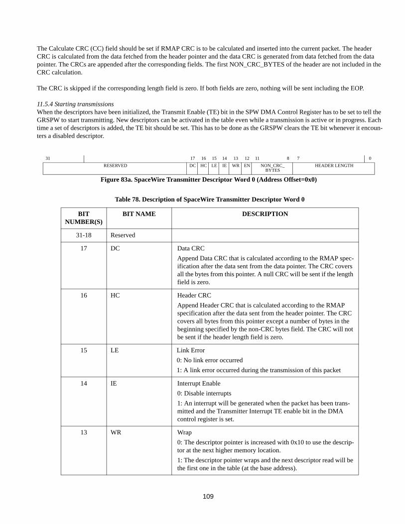
109
The Calculate CRC (CC) field should be set if RMAP CRC is to be calculated and inserted into the current packet. The header CRC is calculated from the data fetched from the header pointer and the data CRC is generated from data fetched from the data pointer. The CRCs are appended after the corresponding fields. The first NON_CRC_BYTES of the header are not included in the CRC calculation.
The CRC is skipped if the corresponding length field is zero. If both fields are zero, nothing will be sent including the EOP.
11.5.4 Starting transmissionsWhen the descriptors have been initialized, the Transmit Enable (TE) bit in the SPW DMA Control Register has to be set to tell the GRSPW to start transmitting. New descriptors can be activated in the table even while a transmission is active or in progress. Each time a set of descriptors is added, the TE bit should be set. This has to be done as the GRSPW clears the TE bit whenever it encoun-ters a disabled descriptor.
Table 78. Description of SpaceWire Transmitter Descriptor Word 0
BIT NUMBER(S)
BIT NAME DESCRIPTION
31-18 Reserved
17 DC Data CRC
Append Data CRC that is calculated according to the RMAP spec-ification after the data sent from the data pointer. The CRC covers all the bytes from this pointer. A null CRC will be sent if the length field is zero.
16 HC Header CRC
Append Header CRC that is calculated according to the RMAP specification after the data sent from the header pointer. The CRC covers all bytes from this pointer except a number of bytes in the beginning specified by the non-CRC bytes field. The CRC will not be sent if the header length field is zero.
15 LE Link Error
0: No link error occurred
1: A link error occurred during the transmission of this packet
14 IE Interrupt Enable
0: Disable interrupts
1: An interrupt will be generated when the packet has been trans-mitted and the Transmitter Interrupt TE enable bit in the DMA control register is set.
13 WR Wrap
0: The descriptor pointer is increased with 0x10 to use the descrip-tor at the next higher memory location.
1: The descriptor pointer wraps and the next descriptor read will be the first one in the table (at the base address).
31 17 16 15 14 13 12 11 8 7 0
RESERVED DC HC LE IE WR EN NON_CRC_ BYTES
HEADER LENGTH
Figure 83a. SpaceWire Transmitter Descriptor Word 0 (Address Offset=0x0)
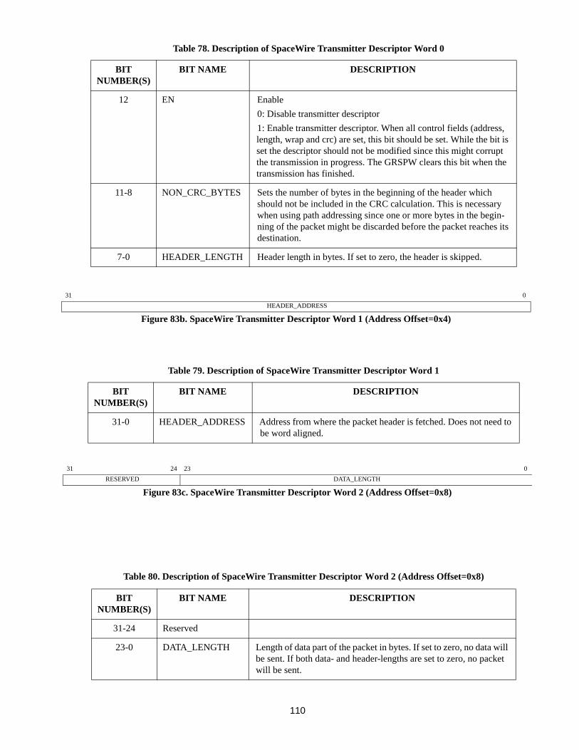
110
BIT NUMBER(S)
BIT NAME DESCRIPTION
12 EN Enable
0: Disable transmitter descriptor
1: Enable transmitter descriptor. When all control fields (address, length, wrap and crc) are set, this bit should be set. While the bit is set the descriptor should not be modified since this might corrupt the transmission in progress. The GRSPW clears this bit when the transmission has finished.
11-8 NON_CRC_BYTES Sets the number of bytes in the beginning of the header which should not be included in the CRC calculation. This is necessary when using path addressing since one or more bytes in the begin-ning of the packet might be discarded before the packet reaches its destination.
7-0 HEADER_LENGTH Header length in bytes. If set to zero, the header is skipped.
Table 79. Description of SpaceWire Transmitter Descriptor Word 1
BIT NUMBER(S)
BIT NAME DESCRIPTION
31-0 HEADER_ADDRESS Address from where the packet header is fetched. Does not need to be word aligned.
Table 80. Description of SpaceWire Transmitter Descriptor Word 2 (Address Offset=0x8)
BIT NUMBER(S)
BIT NAME DESCRIPTION
31-24 Reserved
23-0 DATA_LENGTH Length of data part of the packet in bytes. If set to zero, no data will be sent. If both data- and header-lengths are set to zero, no packet will be sent.
Table 78. Description of SpaceWire Transmitter Descriptor Word 0
31 0
HEADER_ADDRESS
Figure 83b. SpaceWire Transmitter Descriptor Word 1 (Address Offset=0x4)
31 24 23 0
RESERVED DATA_LENGTH
Figure 83c. SpaceWire Transmitter Descriptor Word 2 (Address Offset=0x8)
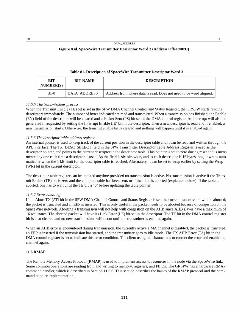
111
11.5.5 The transmissions processWhen the Transmit Enable (TE) bit is set in the SPW DMA Channel Control and Status Register, the GRSPW starts reading descriptors immediately. The number of bytes indicated are read and transmitted. When a transmission has finished, the Enable (EN) field of the descriptor will be cleared and a Packet Sent (PS) bit set in the DMA control register. An interrupt will also be generated if requested by setting the Interrupt Enable (IE) bit in the descriptor. Then a new descriptor is read and if enabled, a new transmission starts. Otherwise, the transmit enable bit is cleared and nothing will happen until it is enabled again.
11.5.6 The descriptor table address registerAn internal pointer is used to keep track of the current position in the descriptor table and it can be read and written through the APB interface. The TX_DESC_SELECT field in the SPW Transmitter Descriptor Table Address Register is used as the descriptor pointer, and points to the current descriptor in the descriptor table. This pointer is set to zero during reset and is incre-mented by one each time a descriptor is used. As the field is six bits wide, and as each descriptor is 16 bytes long, it wraps auto-matically when the 1 kB limit for the descriptor table is reached. Alternately, it can be set to wrap earlier by setting the Wrap (WR) bit in the current descriptor.
The descriptor table register can be updated anytime provided no transmission is active. No transmission is active if the Trans-mit Enable (TE) bit is zero and the complete table has been sent, or if the table is aborted (explained below). If the table is aborted, one has to wait until the TE bit is ‘0’ before updating the table pointer.
11.5.7 Error handlingIf the Abort TX (AT) bit in the SPW DMA Channel Control and Status Register is set, the current transmission will be aborted; the packet is truncated and an EEP is inserted. This is only useful if the packet needs to be aborted because of congestion on the SpaceWire network. Aborting a transmission will not help with congestion on the AHB since AHB slaves have a maximum of 16 waitstates. The aborted packet will have its Link Error (LE) bit set in the descriptor. The TE bit in the DMA control register bit is also cleared and no new transmissions will occur until the transmitter is enabled again.
When an AHB error is encountered during transmission, the currently active DMA channel is disabled, the packet is truncated, an EEP is inserted if the transmission has started, and the transmitter goes to idle mode. The TX AHB Error (TA) bit in the DMA control register is set to indicate this error condition. The client using the channel has to correct the error and enable the channel again.
11.6 RMAP
The Remote Memory Access Protocol (RMAP) is used to implement access to resources in the node via the SpaceWire link. Some common operations are reading from and writing to memory, registers, and FIFOs. The GRSPW has a hardware RMAP command handler, which is described in Section 11.6.6. This section describes the basics of the RMAP protocol and the com-mand handler implementation.
Table 81. Description of SpaceWire Transmitter Descriptor Word 3
BIT NUMBER(S)
BIT NAME DESCRIPTION
31-0 DATA_ADDRESS Address from where data is read. Does not need to be word aligned.
31 0
DATA_ADDRESS
Figure 83d. SpaceWire Transmitter Descriptor Word 3 (Address Offset=0xC)
112
11.6.1 Fundamentals of the protocolRMAP is a protocol that is designed to provide remote access to memory mapped resources on a SpaceWire node via a SpaceWire network. RMAP commands are those that have the Protocol Identifier byte of a SpaceWire packet set to 0x01. RMAP provides three operations: write, read and read-modify-write. These operations are posted operations, which means that a source does not wait for an acknowledge or reply. It also implies that any number of operations can be outstanding at any time and that no timeout mechanism is implemented in the protocol. Time-outs must be implemented in the user appli-cation that sent the commands. Data payloads of up to 16 Mb - 1 are supported by the protocol. A destination can be requested to send replies and to verify data before executing an operation. A complete description of the protocol is found in the RMAP standard.
11.6.2 ImplementationThe GRSPW includes a handler for RMAP commands that processes all incoming packets with protocol ID = 0x01 and Packet Type field in the Command byte set to 0x01. When such a packet is detected, it is not stored to the DMA channel. Instead, it is passed to the RMAP receiver, which is seen in Figure 78.
The GRSPW implements all three commands defined in the standard with some restrictions. The implementation is based on Draft C of the RMAP standard. Support is only provided for 32-bit, big-endian systems. This means that the first byte received is the MSB in a word. The command handler will not receive RMAP packets using the extended protocol ID. These are always sent to the DMA channel.
The RMAP receiver processes commands. If they are correct and accepted, the operation is performed on the AHB bus and a reply is formatted. If an acknowledge is requested, the RMAP transmitter automatically sends the reply. RMAP transmis-sions have priority over DMA channel transmissions.
Packets with a mismatching destination logical address are never passed to the RMAP handler. The DESTINATION_KEY field of the SPW Destination Key Register must match the Destination Key byte of the incoming packet. If there is a mis-match and a reply has been requested, the error code of the Status byte is set to ‘3’. Replies are sent if and only if the Ack field in the Command byte is set to ‘1’.
Detection of all error codes is supported. When a failure occurs during a bus access the error code is set to 1 (General error). There is predetermined order in which error-codes are set in the case of multiple errors in the GRSPW as shown in Table 82.
Table 82. The SpaceWire RMAP Packet Error Codes and Detection Order (Highest Priority is 1)
DETECTION ORDER
ERROR CODE
ERROR ERROR DESCRIPTIONAPPLICABILITY
WRITE READ RMW 0 0 Command
executed successfully
X X X
6* 1 General error code
The detected error does not fit into the other error cases or the node does not support further distinction between the errors
X X X
1 2 Unused RMAP Packet Type or Command Code
The Header CRC was decoded correctly but the packet type is reserved or the command is not used by the RMAP protocol.
X X X
113
Note: *The AHB error is not guaranteed to be detected before Early EOP/EEP or Invalid Data CRC. For very long accesses the AHB error detection might be delayed causing the other two errors to appear first.
Read accesses are performed on the fly; that is, they are not stored in a temporary buffer before transmitting. This means that the error code 1 (General error) will never be seen in a read reply since the header has already been sent when the data is read. If the AHB error occurs, the packet will be truncated and ended with an EEP.
2 3 Invalid key The Header CRC was decoded correctly but the device key did not match that expected by the target user application.
X X X
DETECTION ORDER
ERROR CODE
ERROR ERROR DESCRIPTIONAPPLICABILITY
WRITE READ RMW 11 4 Invalid Data
CRC Error in the CRC of the data field X X
7 5 Early EOP EOP marker detected before the end of the data.
X X X
11 6 Too much data
More than the expected amount of data in a command has been received.
X X X
7 7 EEP EEP marker detected immediately after the header CRC or during the transfer of data and Data CRC or immediately thereafter. Indicates that there was a communication failure of some sort on the network.
X X X
NA 8 Reserved Reserved 3 9 Verify buffer
overrun The verify before write bit of the command was set so that the data field was buffered in order to verify the Data CRC before transferring the data to target memory. The data field was longer than able to fit inside the verify buffer resulting in a buffer overrun. Note that the command is not executed in this case.
X X
5 10 RMAP Command not implemented or not authorized
The target user application did not authorize the requested operation. This may be because the command requested has not been implemented.
X X X
4 11 RMW Data Length error
The amount of data in a RMW command is invalid (0x01, 0x03, 0x05, 0x07 or greater than 0x08).
X
12 12 Invalid Target Logical Address
The Header CRC was decoded correctly but the Target Logical Address was not the value expected by the target.
X X X
Table 82. The SpaceWire RMAP Packet Error Codes and Detection Order (Highest Priority is 1)
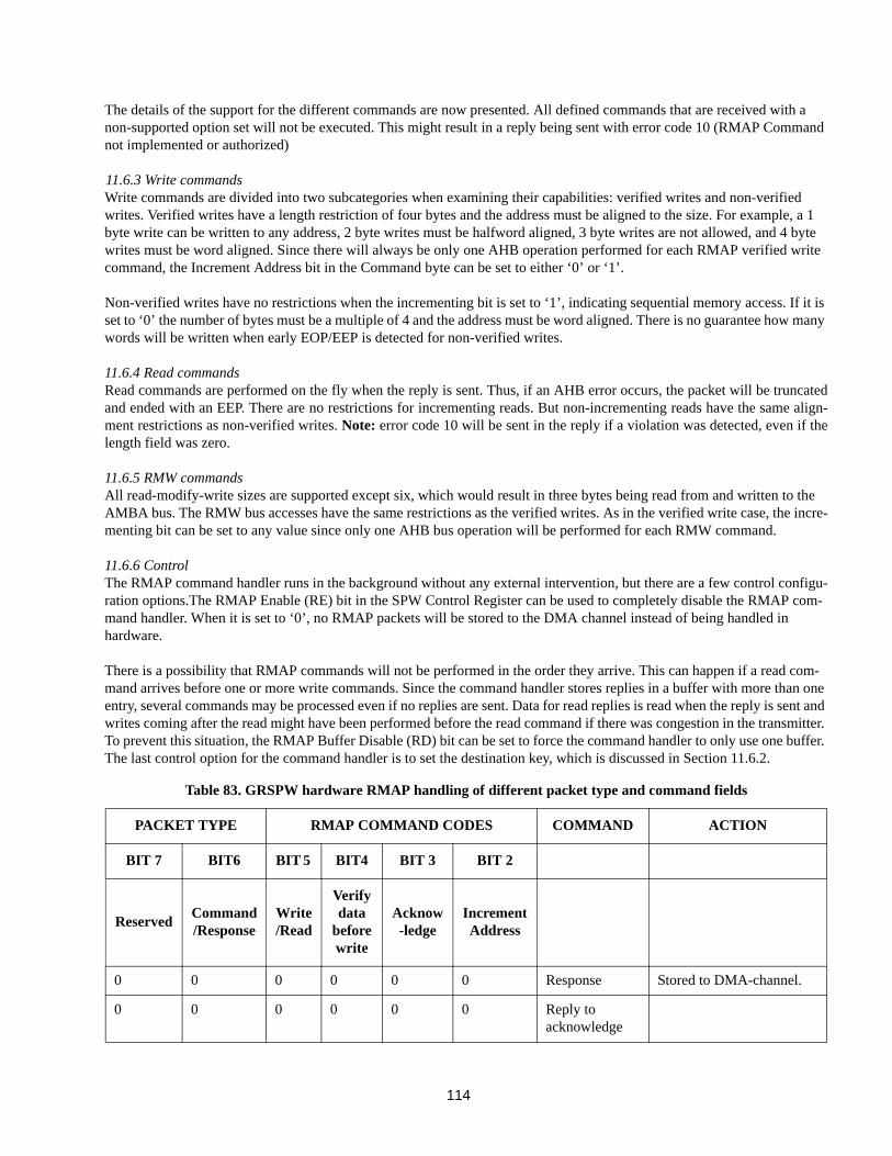
114
The details of the support for the different commands are now presented. All defined commands that are received with a non-supported option set will not be executed. This might result in a reply being sent with error code 10 (RMAP Command not implemented or authorized)
11.6.3 Write commandsWrite commands are divided into two subcategories when examining their capabilities: verified writes and non-verified writes. Verified writes have a length restriction of four bytes and the address must be aligned to the size. For example, a 1 byte write can be written to any address, 2 byte writes must be halfword aligned, 3 byte writes are not allowed, and 4 byte writes must be word aligned. Since there will always be only one AHB operation performed for each RMAP verified write command, the Increment Address bit in the Command byte can be set to either ‘0’ or ‘1’.
Non-verified writes have no restrictions when the incrementing bit is set to ‘1’, indicating sequential memory access. If it is set to ‘0’ the number of bytes must be a multiple of 4 and the address must be word aligned. There is no guarantee how many words will be written when early EOP/EEP is detected for non-verified writes.
11.6.4 Read commandsRead commands are performed on the fly when the reply is sent. Thus, if an AHB error occurs, the packet will be truncatedand ended with an EEP. There are no restrictions for incrementing reads. But non-incrementing reads have the same align-ment restrictions as non-verified writes. Note: error code 10 will be sent in the reply if a violation was detected, even if thelength field was zero.
11.6.5 RMW commandsAll read-modify-write sizes are supported except six, which would result in three bytes being read from and written to the AMBA bus. The RMW bus accesses have the same restrictions as the verified writes. As in the verified write case, the incre-menting bit can be set to any value since only one AHB bus operation will be performed for each RMW command.
11.6.6 ControlThe RMAP command handler runs in the background without any external intervention, but there are a few control configu-ration options.The RMAP Enable (RE) bit in the SPW Control Register can be used to completely disable the RMAP com-mand handler. When it is set to ‘0’, no RMAP packets will be stored to the DMA channel instead of being handled in hardware.
There is a possibility that RMAP commands will not be performed in the order they arrive. This can happen if a read com-mand arrives before one or more write commands. Since the command handler stores replies in a buffer with more than one entry, several commands may be processed even if no replies are sent. Data for read replies is read when the reply is sent and writes coming after the read might have been performed before the read command if there was congestion in the transmitter. To prevent this situation, the RMAP Buffer Disable (RD) bit can be set to force the command handler to only use one buffer. The last control option for the command handler is to set the destination key, which is discussed in Section 11.6.2.
Table 83. GRSPW hardware RMAP handling of different packet type and command fields
PACKET TYPE RMAP COMMAND CODES COMMAND ACTION
BIT 7 BIT6 BIT 5 BIT4 BIT 3 BIT 2
ReservedCommand /Response
Write /Read
Verify data
before write
Acknow-ledge
Increment Address
0 0 0 0 0 0 Response Stored to DMA-channel.
0 0 0 0 0 0 Reply to acknowledge
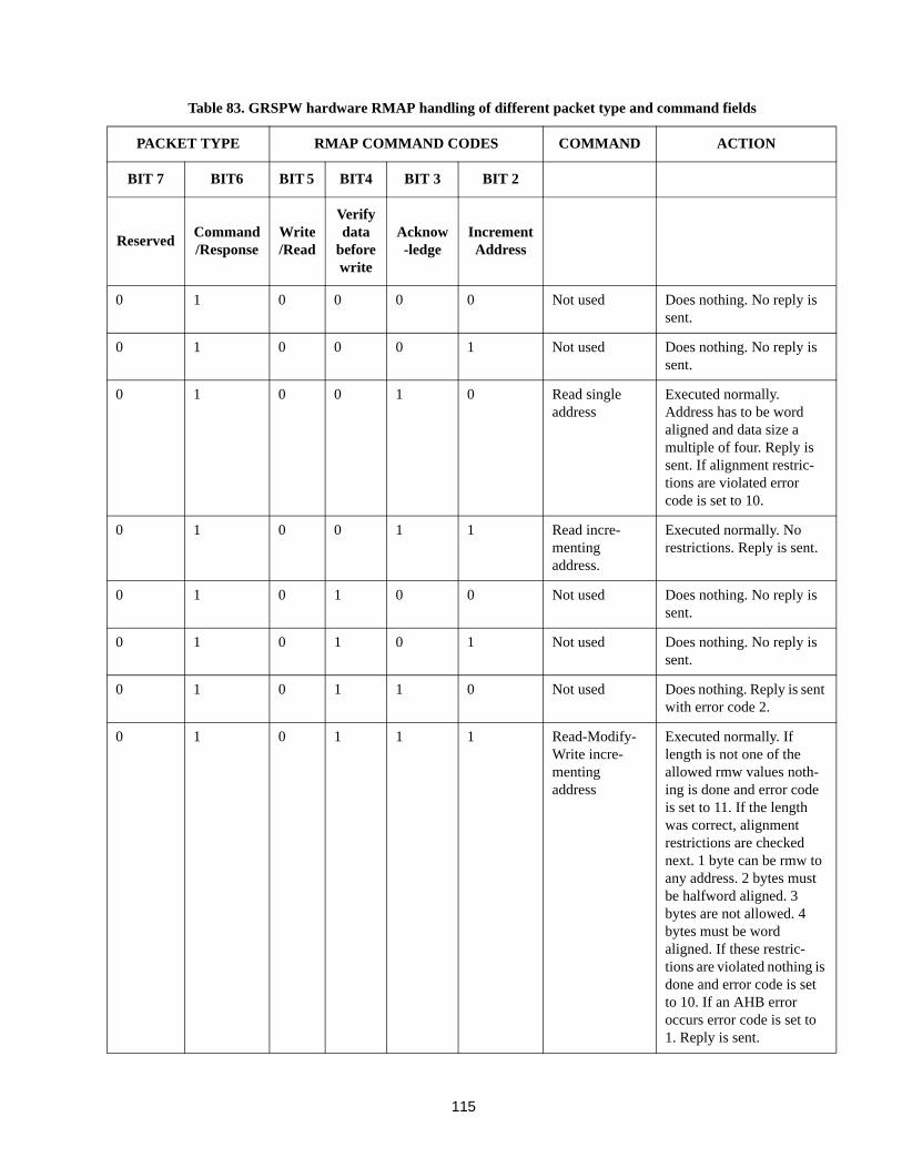
115
0 1 0 0 0 0 Not used Does nothing. No reply is sent.
0 1 0 0 0 1 Not used Does nothing. No reply is sent.
0 1 0 0 1 0 Read single address
Executed normally. Address has to be word aligned and data size a multiple of four. Reply is sent. If alignment restric-tions are violated error code is set to 10.
0 1 0 0 1 1 Read incre-menting address.
Executed normally. No restrictions. Reply is sent.
0 1 0 1 0 0 Not used Does nothing. No reply is sent.
0 1 0 1 0 1 Not used Does nothing. No reply is sent.
0 1 0 1 1 0 Not used Does nothing. Reply is sent with error code 2.
0 1 0 1 1 1 Read-Modify-Write incre-menting address
Executed normally. If length is not one of the allowed rmw values noth-ing is done and error code is set to 11. If the length was correct, alignment restrictions are checked next. 1 byte can be rmw to any address. 2 bytes must be halfword aligned. 3 bytes are not allowed. 4 bytes must be word aligned. If these restric-tions are violated nothing is done and error code is set to 10. If an AHB error occurs error code is set to 1. Reply is sent.
Table 83. GRSPW hardware RMAP handling of different packet type and command fields
PACKET TYPE RMAP COMMAND CODES COMMAND ACTION
BIT 7 BIT6 BIT 5 BIT4 BIT 3 BIT 2
ReservedCommand /Response
Write /Read
Verify data
before write
Acknow-ledge
Increment Address
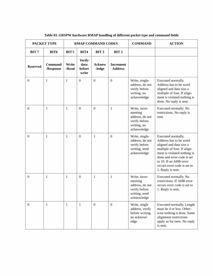
0 1 1 0 0 0 Write, single-address, do not verify before writing, no acknowledge
Executed normally. Address has to be word aligned and data size a multiple of four. If align-ment is violated nothing is done. No reply is sent.
0 1 1 0 0 1 Write, incre-menting address, do not verify before writing, no acknowledge
Executed normally. No restrictions. No reply is sent.
0 1 1 0 1 0 Write, single-address, do not verify before writing, send acknowledge
Executed normally. Address has to be word aligned and data size a multiple of four. If align-ment is violated nothing is done and error code is set to 10. If an AHB error occurs error code is set to 1. Reply is sent.
0 1 1 0 1 1 Write, incre-menting address, do not verify before writing, send acknowledge
Executed normally. No restrictions. If AHB error occurs error code is set to 1. Reply is sent.
0 1 1 1 0 0 Write, single address, verify before writing, no acknowl-edge
Executed normally. Length must be 4 or less. Other-wise nothing is done. Same alignment restrictions apply as for rmw. No reply is sent.
Table 83. GRSPW hardware RMAP handling of different packet type and command fields
PACKET TYPE RMAP COMMAND CODES COMMAND ACTION
BIT 7 BIT6 BIT 5 BIT4 BIT 3 BIT 2
ReservedCommand /Response
Write /Read
Verify data
before write
Acknow-ledge
Increment Address
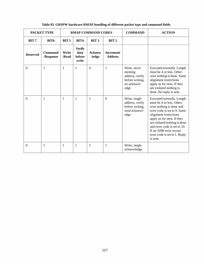
117
0 1 1 1 0 1 Write, incre-menting address, verify before writing, no acknowl-edge
Executed normally. Length must be 4 or less. Other-wise nothing is done. Same alignment restrictions apply as for rmw. If they are violated nothing is done. No reply is sent.
0 1 1 1 1 0 Write, single address, verify before writing, send acknowl-edge
Executed normally. Length must be 4 or less. Other-wise nothing is done and error code is set to 9. Same alignment restrictions apply as for rmw. If they are violated nothing is done and error code is set to 10. If an AHB error occurs error code is set to 1. Reply is sent.
0 1 1 1 1 1 Write, single acknowledge
Table 83. GRSPW hardware RMAP handling of different packet type and command fields
PACKET TYPE RMAP COMMAND CODES COMMAND ACTION
BIT 7 BIT6 BIT 5 BIT4 BIT 3 BIT 2
ReservedCommand /Response
Write /Read
Verify data
before write
Acknow-ledge
Increment Address
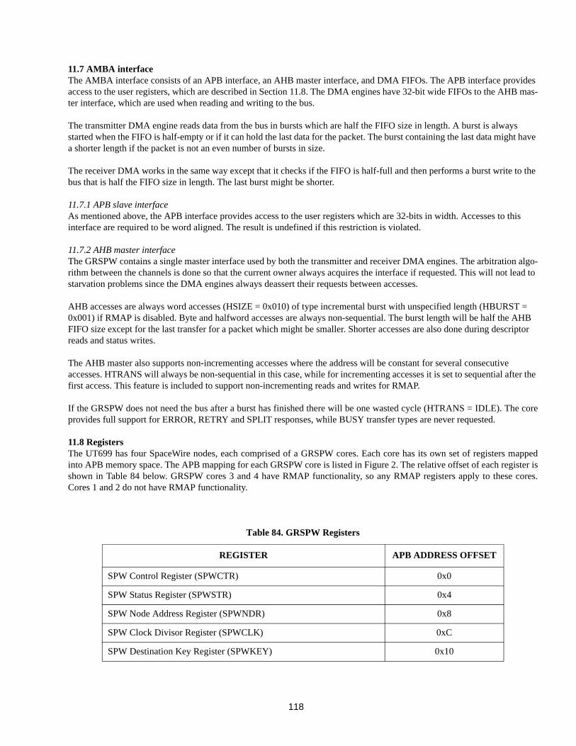
118
11.7 AMBA interfaceThe AMBA interface consists of an APB interface, an AHB master interface, and DMA FIFOs. The APB interface provides access to the user registers, which are described in Section 11.8. The DMA engines have 32-bit wide FIFOs to the AHB mas-ter interface, which are used when reading and writing to the bus.
The transmitter DMA engine reads data from the bus in bursts which are half the FIFO size in length. A burst is always started when the FIFO is half-empty or if it can hold the last data for the packet. The burst containing the last data might have a shorter length if the packet is not an even number of bursts in size.
The receiver DMA works in the same way except that it checks if the FIFO is half-full and then performs a burst write to the bus that is half the FIFO size in length. The last burst might be shorter.
11.7.1 APB slave interfaceAs mentioned above, the APB interface provides access to the user registers which are 32-bits in width. Accesses to this interface are required to be word aligned. The result is undefined if this restriction is violated.
11.7.2 AHB master interfaceThe GRSPW contains a single master interface used by both the transmitter and receiver DMA engines. The arbitration algo-rithm between the channels is done so that the current owner always acquires the interface if requested. This will not lead to starvation problems since the DMA engines always deassert their requests between accesses.
AHB accesses are always word accesses (HSIZE = 0x010) of type incremental burst with unspecified length (HBURST = 0x001) if RMAP is disabled. Byte and halfword accesses are always non-sequential. The burst length will be half the AHB FIFO size except for the last transfer for a packet which might be smaller. Shorter accesses are also done during descriptor reads and status writes.
The AHB master also supports non-incrementing accesses where the address will be constant for several consecutive accesses. HTRANS will always be non-sequential in this case, while for incrementing accesses it is set to sequential after the first access. This feature is included to support non-incrementing reads and writes for RMAP.
If the GRSPW does not need the bus after a burst has finished there will be one wasted cycle (HTRANS = IDLE). The coreprovides full support for ERROR, RETRY and SPLIT responses, while BUSY transfer types are never requested.
11.8 Registers The UT699 has four SpaceWire nodes, each comprised of a GRSPW cores. Each core has its own set of registers mappedinto APB memory space. The APB mapping for each GRSPW core is listed in Figure 2. The relative offset of each register isshown in Table 84 below. GRSPW cores 3 and 4 have RMAP functionality, so any RMAP registers apply to these cores.Cores 1 and 2 do not have RMAP functionality.
Table 84. GRSPW Registers
REGISTER APB ADDRESS OFFSET
SPW Control Register (SPWCTR) 0x0
SPW Status Register (SPWSTR) 0x4
SPW Node Address Register (SPWNDR) 0x8
SPW Clock Divisor Register (SPWCLK) 0xC
SPW Destination Key Register (SPWKEY) 0x10
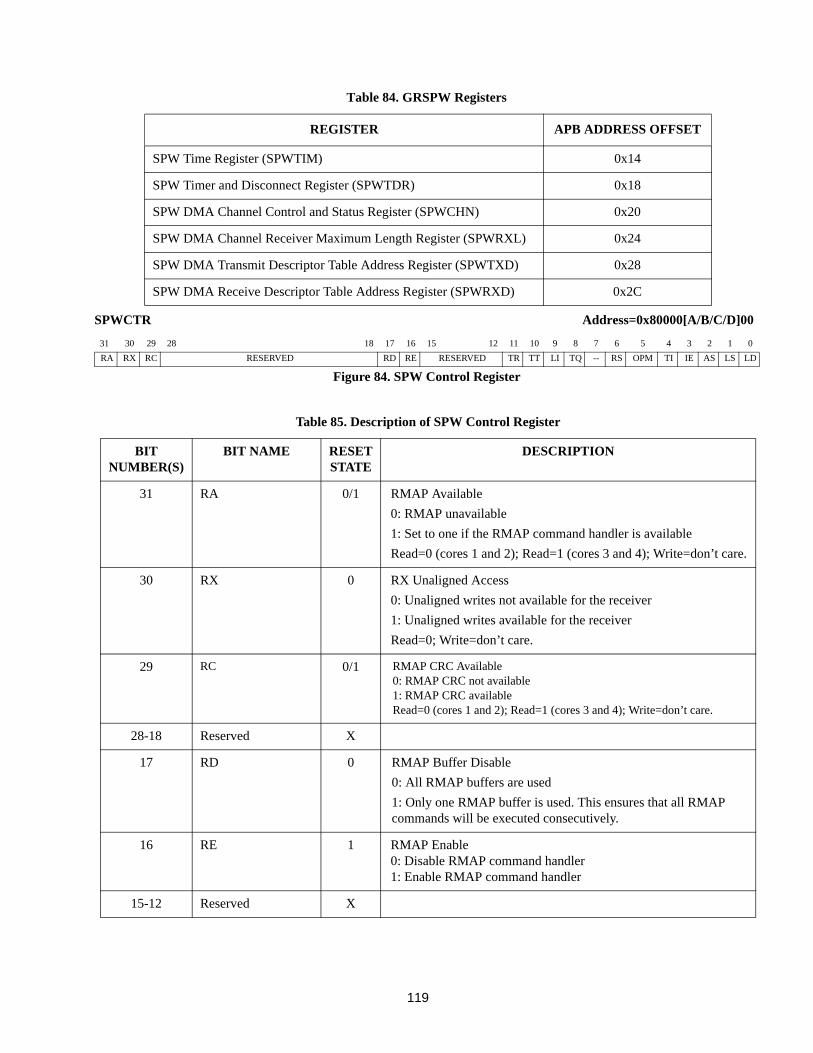
119
SPW Time Register (SPWTIM) 0x14
SPW Timer and Disconnect Register (SPWTDR) 0x18
SPW DMA Channel Control and Status Register (SPWCHN) 0x20
SPW DMA Channel Receiver Maximum Length Register (SPWRXL) 0x24
SPW DMA Transmit Descriptor Table Address Register (SPWTXD) 0x28
SPW DMA Receive Descriptor Table Address Register (SPWRXD) 0x2C
Table 85. Description of SPW Control Register
BIT NUMBER(S)
BIT NAME RESET STATE
DESCRIPTION
31 RA 0/1 RMAP Available
0: RMAP unavailable
1: Set to one if the RMAP command handler is available
Read=0 (cores 1 and 2); Read=1 (cores 3 and 4); Write=don’t care.
30 RX 0 RX Unaligned Access
0: Unaligned writes not available for the receiver
1: Unaligned writes available for the receiver
Read=0; Write=don’t care.
29 RC 0/1 RMAP CRC Available0: RMAP CRC not available1: RMAP CRC availableRead=0 (cores 1 and 2); Read=1 (cores 3 and 4); Write=don’t care.
28-18 Reserved X
17 RD 0 RMAP Buffer Disable
0: All RMAP buffers are used
1: Only one RMAP buffer is used. This ensures that all RMAP commands will be executed consecutively.
16 RE 1 RMAP Enable0: Disable RMAP command handler1: Enable RMAP command handler
15-12 Reserved X
Table 84. GRSPW Registers
REGISTER APB ADDRESS OFFSET
SPWCTR Address=0x80000[A/B/C/D]00
31 30 29 28 18 17 16 15 12 11 10 9 8 7 6 5 4 3 2 1 0
RA RX RC RESERVED RD RE RESERVED TR TT LI TQ -- RS OPM TI IE AS LS LD
Figure 84. SPW Control Register
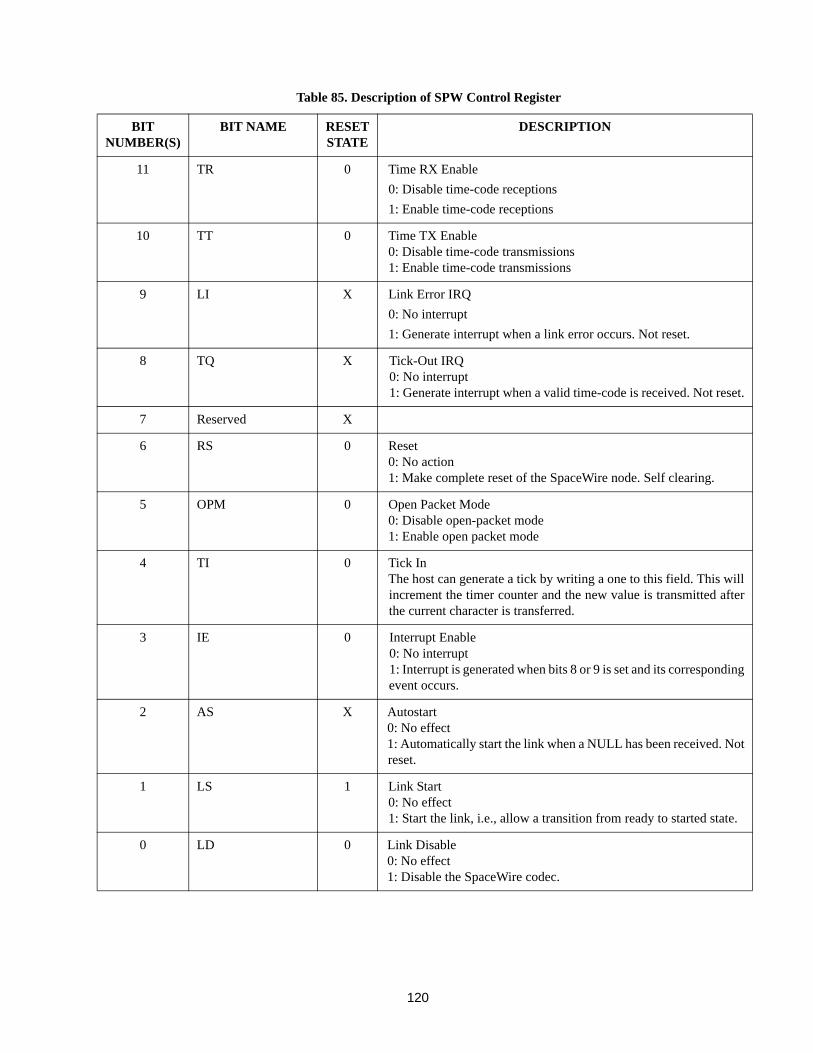
120
BIT NUMBER(S)
BIT NAME RESET STATE
DESCRIPTION
11 TR 0 Time RX Enable
0: Disable time-code receptions
1: Enable time-code receptions
10 TT 0 Time TX Enable0: Disable time-code transmissions1: Enable time-code transmissions
9 LI X Link Error IRQ
0: No interrupt
1: Generate interrupt when a link error occurs. Not reset.
8 TQ X Tick-Out IRQ0: No interrupt1: Generate interrupt when a valid time-code is received. Not reset.
7 Reserved X
6 RS 0 Reset0: No action1: Make complete reset of the SpaceWire node. Self clearing.
5 OPM 0 Open Packet Mode0: Disable open-packet mode1: Enable open packet mode
4 TI 0 Tick InThe host can generate a tick by writing a one to this field. This willincrement the timer counter and the new value is transmitted afterthe current character is transferred.
3 IE 0 Interrupt Enable0: No interrupt1: Interrupt is generated when bits 8 or 9 is set and its correspondingevent occurs.
2 AS X Autostart0: No effect1: Automatically start the link when a NULL has been received. Notreset.
1 LS 1 Link Start0: No effect1: Start the link, i.e., allow a transition from ready to started state.
0 LD 0 Link Disable0: No effect1: Disable the SpaceWire codec.
Table 85. Description of SPW Control Register
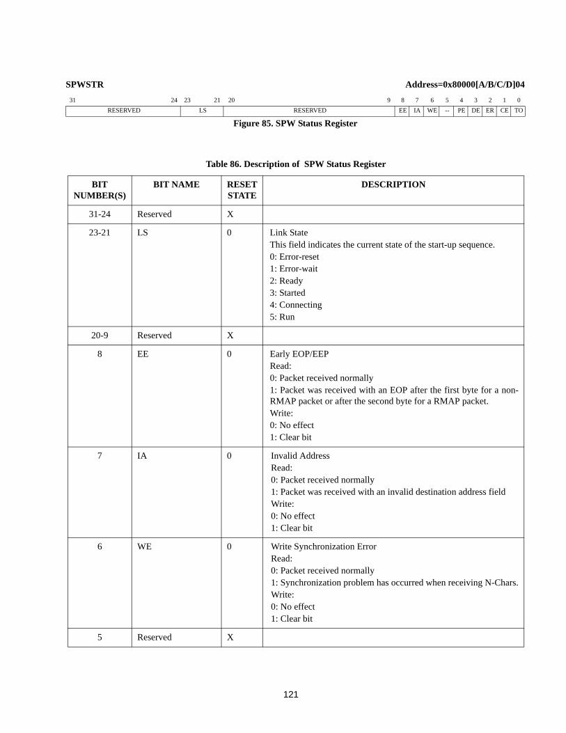
121
Table 86. Description of SPW Status Register
BIT NUMBER(S)
BIT NAME RESET STATE
DESCRIPTION
31-24 Reserved X
23-21 LS 0 Link StateThis field indicates the current state of the start-up sequence.0: Error-reset1: Error-wait2: Ready3: Started4: Connecting5: Run
20-9 Reserved X
8 EE 0 Early EOP/EEPRead:0: Packet received normally1: Packet was received with an EOP after the first byte for a non-RMAP packet or after the second byte for a RMAP packet.Write:0: No effect1: Clear bit
7 IA 0 Invalid AddressRead:0: Packet received normally1: Packet was received with an invalid destination address fieldWrite:0: No effect1: Clear bit
6 WE 0 Write Synchronization ErrorRead:0: Packet received normally1: Synchronization problem has occurred when receiving N-Chars.Write:0: No effect1: Clear bit
5 Reserved X
SPWSTR Address=0x80000[A/B/C/D]04
31 24 23 21 20 9 8 7 6 5 4 3 2 1 0
RESERVED LS RESERVED EE IA WE -- PE DE ER CE TO
Figure 85. SPW Status Register
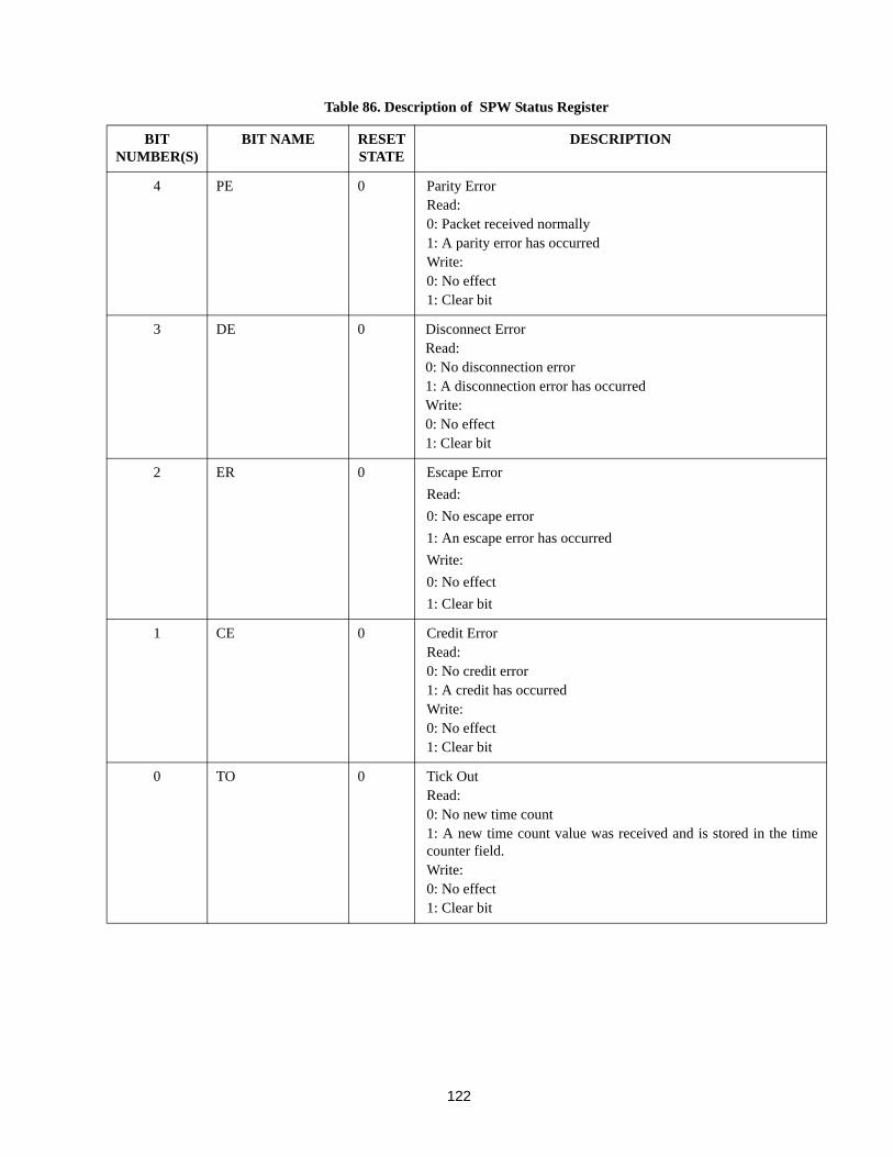
122
BIT NUMBER(S)
BIT NAME RESET STATE
DESCRIPTION
4 PE 0 Parity ErrorRead:0: Packet received normally1: A parity error has occurredWrite:0: No effect1: Clear bit
3 DE 0 Disconnect ErrorRead:0: No disconnection error1: A disconnection error has occurredWrite:0: No effect1: Clear bit
2 ER 0 Escape Error
Read:
0: No escape error
1: An escape error has occurred
Write:
0: No effect
1: Clear bit
1 CE 0 Credit ErrorRead:0: No credit error1: A credit has occurredWrite:0: No effect1: Clear bit
0 TO 0 Tick OutRead:0: No new time count1: A new time count value was received and is stored in the timecounter field.Write:0: No effect1: Clear bit
Table 86. Description of SPW Status Register
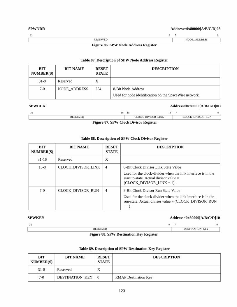
123
Table 87. Description of SPW Node Address Register
BIT NUMBER(S)
BIT NAME RESET STATE
DESCRIPTION
31-8 Reserved X
7-0 NODE_ADDRESS 254 8-Bit Node Address
Used for node identification on the SpaceWire network.
Table 88. Description of SPW Clock Divisor Register
BIT NUMBER(S)
BIT NAME RESET STATE
DESCRIPTION
31-16 Reserved X
15-8 CLOCK_DIVISOR_LINK 4 8-Bit Clock Divisor Link State Value
Used for the clock-divider when the link interface is in the startup-state. Actual divisor value = (CLOCK_DIVISOR_LINK + 1).
7-0 CLOCK_DIVISOR_RUN 4 8-Bit Clock Divisor Run State Value
Used for the clock-divider when the link interface is in the run-state. Actual divisor value = (CLOCK_DIVISOR_RUN + 1).
Table 89. Description of SPW Destination Key Register
BIT NUMBER(S)
BIT NAME RESET STATE
DESCRIPTION
31-8 Reserved X
7-0 DESTINATION_KEY 0 RMAP Destination Key
SPWKEY Address=0x80000[A/B/C/D]10
31 8 7 0
RESERVED DESTINATION_KEY
Figure 88. SPW Destination Key Register
SPWCLK Address=0x80000[A/B/C/D]0C
31 16 15 8 7 0
RESERVED CLOCK_DIVISOR_LINK CLOCK_DIVISOR_RUN
Figure 87. SPW Clock Divisor Register
SPWNDR Address=0x80000[A/B/C/D]08
31 8 7 0
RESERVED NODE_ ADDRESS
Figure 86. SPW Node Address Register
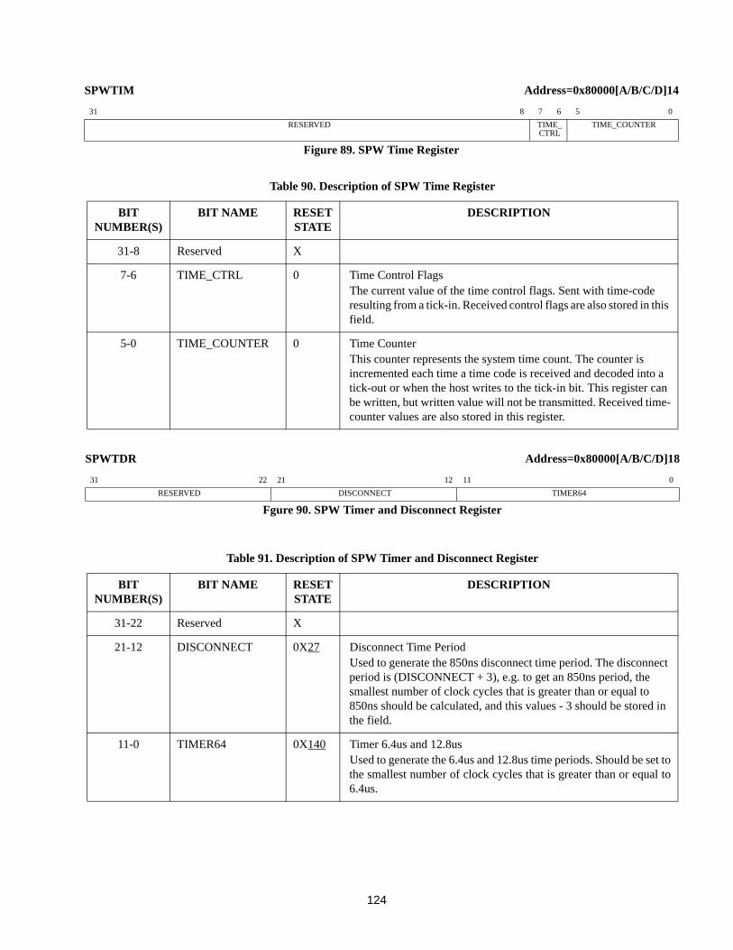
124
Table 90. Description of SPW Time Register
BIT NUMBER(S)
BIT NAME RESET STATE
DESCRIPTION
31-8 Reserved X
7-6 TIME_CTRL 0 Time Control FlagsThe current value of the time control flags. Sent with time-code resulting from a tick-in. Received control flags are also stored in this field.
5-0 TIME_COUNTER 0 Time CounterThis counter represents the system time count. The counter is incremented each time a time code is received and decoded into a tick-out or when the host writes to the tick-in bit. This register can be written, but written value will not be transmitted. Received time-counter values are also stored in this register.
Table 91. Description of SPW Timer and Disconnect Register
BIT NUMBER(S)
BIT NAME RESET STATE
DESCRIPTION
31-22 Reserved X
21-12 DISCONNECT 0X27 Disconnect Time PeriodUsed to generate the 850ns disconnect time period. The disconnect period is (DISCONNECT + 3), e.g. to get an 850ns period, the smallest number of clock cycles that is greater than or equal to 850ns should be calculated, and this values - 3 should be stored in the field.
11-0 TIMER64 0X140 Timer 6.4us and 12.8usUsed to generate the 6.4us and 12.8us time periods. Should be set tothe smallest number of clock cycles that is greater than or equal to6.4us.
SPWTDR Address=0x80000[A/B/C/D]18
31 22 21 12 11 0
RESERVED DISCONNECT TIMER64
Fgure 90. SPW Timer and Disconnect Register
SPWTIM Address=0x80000[A/B/C/D]14
31 8 7 6 5 0
RESERVED TIME_CTRL
TIME_COUNTER
Figure 89. SPW Time Register
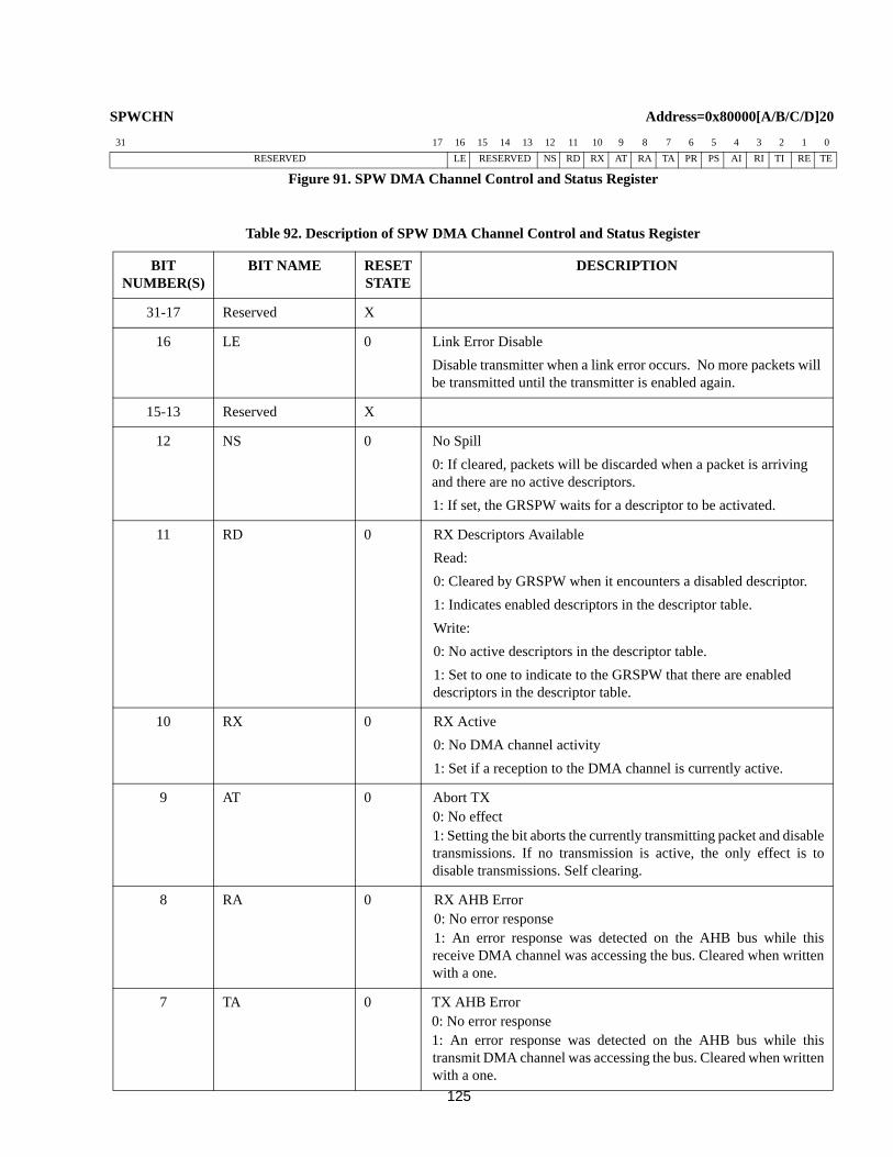
125
Table 92. Description of SPW DMA Channel Control and Status Register
BIT NUMBER(S)
BIT NAME RESET STATE
DESCRIPTION
31-17 Reserved X
16 LE 0 Link Error Disable
Disable transmitter when a link error occurs. No more packets will be transmitted until the transmitter is enabled again.
15-13 Reserved X
12 NS 0 No Spill
0: If cleared, packets will be discarded when a packet is arriving and there are no active descriptors.
1: If set, the GRSPW waits for a descriptor to be activated.
11 RD 0 RX Descriptors Available
Read:
0: Cleared by GRSPW when it encounters a disabled descriptor.
1: Indicates enabled descriptors in the descriptor table.
Write:
0: No active descriptors in the descriptor table.
1: Set to one to indicate to the GRSPW that there are enabled descriptors in the descriptor table.
10 RX 0 RX Active
0: No DMA channel activity
1: Set if a reception to the DMA channel is currently active.
9 AT 0 Abort TX0: No effect1: Setting the bit aborts the currently transmitting packet and disabletransmissions. If no transmission is active, the only effect is todisable transmissions. Self clearing.
8 RA 0 RX AHB Error0: No error response1: An error response was detected on the AHB bus while thisreceive DMA channel was accessing the bus. Cleared when writtenwith a one.
7 TA 0 TX AHB Error0: No error response1: An error response was detected on the AHB bus while thistransmit DMA channel was accessing the bus. Cleared when writtenwith a one.
SPWCHN Address=0x80000[A/B/C/D]20
31 17 16 15 14 13 12 11 10 9 8 7 6 5 4 3 2 1 0
RESERVED LE RESERVED NS RD RX AT RA TA PR PS AI RI TI RE TE
Figure 91. SPW DMA Channel Control and Status Register
126
BIT NUMBER(S)
BIT NAME RESET STATE
DESCRIPTION
6 PR 0 Packet Received0: No new packet1: This bit is set each time a packet has been received. Not selfclearing. Cleared when written with a one.
5 PS 0 Packet Sent0: No packet sent1: This bit is set each time a packet has been sent. Not self clearing.Cleared when written with a one.
4 AI X AHB Error Interrupt0: No interrupt will be generated1: If set, an interrupt will be generated each time an AHB erroroccurs when this DMA channel is accessing the bus. Not reset.
3 RI X Receive Interrupt0: No interrupt will be generated1: If set, an interrupt will be generated each time a packet has beenreceived. This happens if either the packet is terminated by an EEPor EOP. Not reset.
2 TI X Transmit Interrupt0: No interrupt will be generated1: If set, an interrupt will be generated each time a packet is transmitted. The interrupt is generated regardless of whether the transmission was successful or not. Not reset.
1 RE 0 Receiver Enable0: Channel is not allowed to receive packets1: Channel is allowed to receive packets
0 TE 0 Transmitter EnableRead:0: Cleared by GRSPW when it encounters a disabled descriptor.
1: Indicates enabled descriptors in the descriptor table.
Write:
0: No active descriptors in the descriptor table.
1: Set to one to indicate to the GRSPW that there are enabled descriptors in the descriptor table. Writing a one will cause the GRSPW to read a new descriptor and try to transmit the packet to which it points.
Table 92. Description of SPW DMA Channel Control and Status Register
127
Table 93. Description of SPW DMA Channel Receiver Max Length Register
BIT NUMBER(S)
BIT NAME RESET STATE
DESCRIPTION
31-25 Reserved X
24-0 RX_MAX_LENGTH X Receiver Packet Maximum LengthThe maximum number of bytes in a packet that may be received.Only bits 24-2 are writable. Bits 1-0 always read 0. Not reset.
Table 94. Description of SPW Transmitter Descriptor Table Address Register
BIT NUMBER(S)
BIT NAME RESET STATE
DESCRIPTION
31-10 TX_BASE_ADDRESS X Transmitter Descriptor Table Base AddressSets the base address of the descriptor table. Not reset.
9-4 TX_DESC_SELECT 0 Transmitter Descriptor SelectorThis is the relative offset into the descriptor table and indicateswhich descriptor is currently used by the GRSPW. For each newdescriptor read, TX_DESC_SELECT will increase by one andwrap to zero when the field increments to 64.
3-0 Reserved X
Table 95. Description of SPW Receiver Descriptor Table Address Register
BIT NUMBER(S)
BIT NAME RESET STATE
DESCRIPTION
31-10 RX_BASE_ADDRESS X Receiver Descriptor Table Base AddressSets the base address of the descriptor table. Not reset.
9-3 RX_DESC_SELECT 0 Receiver Descriptor SelectorThis is the relative offset into the descriptor table and indicateswhich descriptor is currently used by the GRSPW. For each newdescriptor read, RX_DESC_SELECT will increase by one andwrap to zero when the field increments to 128.
2-0 Reserved X
SPWRXL Address=0x80000[A/B/C/D]24
31 25 24 0
RESERVED RX_MAX_LENGTH
Figure 92. SPW DMA Channel Receiver Max Length Register
SPWTXD Address=0x80000[A/B/C/D]28
31 10 9 4 3 0
TX_BASE_ADDRESS TX_DESC_SELECT RES
Figure 93. SPW Transmitter Descriptor Table Address Register
SPWRXD Address=0x80000[A/B/C/D]2C
31 10 9 3 2 0
RX_BASE_ADDRESS RX_DESC_SELECT RES
Figure 94. SPW Receiver Descriptor Table Address Register
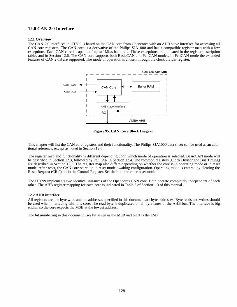
128
12.0 CAN-2.0 Interface
12.1 OverviewThe CAN-2.0 interfaces in UT699 is based on the CAN core from Opencores with an AHB slave interface for accessing allCAN core registers. The CAN core is a derivative of the Philips SJA1000 and has a compatible register map with a fewexceptions. Each CAN core is capable of up to 1Mb/s band rate. These exceptions are indicated in the register descriptiontables and in Section 12.6. The CAN core supports both BasicCAN and PeliCAN modes. In PeliCAN mode the extendedfeatures of CAN 2.0B are supported. The mode of operation is chosen through the clock divider register.
This chapter will list the CAN core registers and their functionality. The Philips SJA1000 data sheet can be used as an addi-tional reference, except as noted in Section 12.6.
The register map and functionality is different depending upon which mode of operation is selected. BasicCAN mode willbe described in Section 12.3, followed by PeliCAN in Section 12.4. The common registers (Clock Divisor and Bus Timing)are described in Section 12.5. The register map also differs depending on whether the core is in operating mode or in resetmode. After reset, the CAN core starts up in reset mode awaiting configuration. Operating mode is entered by clearing theReset Request (CR.0) bit in the Control Register. Set the bit to re-enter reset mode.
The UT699 implements two identical instances of the Opencores CAN core. Both operate completely independent of eachother. The AHB register mapping for each core is indicated in Table 2 of Section 1.3 of this manual.
12.2 AHB interfaceAll registers are one byte wide and the addresses specified in this document are byte addresses. Byte reads and writes shouldbe used when interfacing with this core. The read byte is duplicated on all byte lanes of the AHB bus. The interface is bigendian so the core expects the MSB at the lowest address.
The bit numbering in this document uses bit seven as the MSB and bit 0 as the LSB.
Figure 95. CAN Core Block Diagram
AHB slave interface
AMBA AHB
Buffer RAMCAN CoreCAN_RXI
CAN_TXO
CAN Core with AHB
IRQ
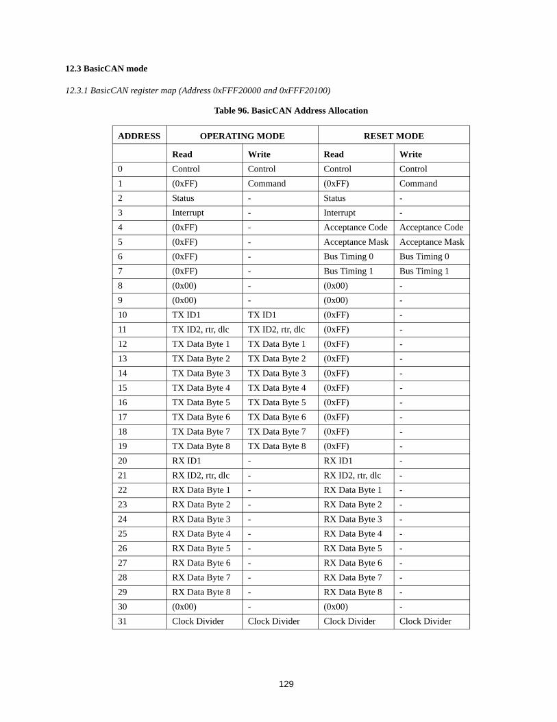
129
12.3 BasicCAN mode
12.3.1 BasicCAN register map (Address 0xFFF20000 and 0xFFF20100)
Table 96. BasicCAN Address Allocation
ADDRESS OPERATING MODE RESET MODE
Read Write Read Write
0 Control Control Control Control
1 (0xFF) Command (0xFF) Command
2 Status - Status -
3 Interrupt - Interrupt -
4 (0xFF) - Acceptance Code Acceptance Code
5 (0xFF) - Acceptance Mask Acceptance Mask
6 (0xFF) - Bus Timing 0 Bus Timing 0
7 (0xFF) - Bus Timing 1 Bus Timing 1
8 (0x00) - (0x00) -
9 (0x00) - (0x00) -
10 TX ID1 TX ID1 (0xFF) -
11 TX ID2, rtr, dlc TX ID2, rtr, dlc (0xFF) -
12 TX Data Byte 1 TX Data Byte 1 (0xFF) -
13 TX Data Byte 2 TX Data Byte 2 (0xFF) -
14 TX Data Byte 3 TX Data Byte 3 (0xFF) -
15 TX Data Byte 4 TX Data Byte 4 (0xFF) -
16 TX Data Byte 5 TX Data Byte 5 (0xFF) -
17 TX Data Byte 6 TX Data Byte 6 (0xFF) -
18 TX Data Byte 7 TX Data Byte 7 (0xFF) -
19 TX Data Byte 8 TX Data Byte 8 (0xFF) -
20 RX ID1 - RX ID1 -
21 RX ID2, rtr, dlc - RX ID2, rtr, dlc -
22 RX Data Byte 1 - RX Data Byte 1 -
23 RX Data Byte 2 - RX Data Byte 2 -
24 RX Data Byte 3 - RX Data Byte 3 -
25 RX Data Byte 4 - RX Data Byte 4 -
26 RX Data Byte 5 - RX Data Byte 5 -
27 RX Data Byte 6 - RX Data Byte 6 -
28 RX Data Byte 7 - RX Data Byte 7 -
29 RX Data Byte 8 - RX Data Byte 8 -
30 (0x00) - (0x00) -
31 Clock Divider Clock Divider Clock Divider Clock Divider
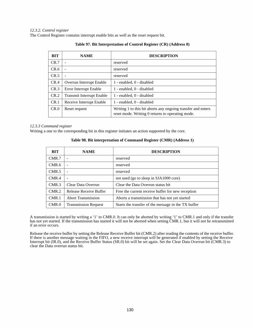
130
12.3.2. Control registerThe Control Register contains interrupt enable bits as well as the reset request bit.
12.3.3 Command registerWriting a one to the corresponding bit in this register initiates an action supported by the core.
A transmission is started by writing a ‘1’ to CMR.0. It can only be aborted by writing ‘1’ to CMR.1 and only if the transfer has not yet started. If the transmission has started it will not be aborted when setting CMR.1, but it will not be retransmitted if an error occurs.
Release the receive buffer by setting the Release Receive Buffer bit (CMR.2) after reading the contents of the receive buffer. If there is another message waiting in the FIFO, a new receive interrupt will be generated if enabled by setting the Receive Interrupt bit (IR.0), and the Receive Buffer Status (SR.0) bit will be set again. Set the Clear Data Overrun bit (CMR.3) to clear the Data overrun status bit.
Table 97. Bit Interpretation of Control Register (CR) (Address 0)
BIT NAME DESCRIPTION
CR.7 - reserved
CR.6 - reserved
CR.5 - reserved
CR.4 Overrun Interrupt Enable 1 - enabled, 0 - disabled
CR.3 Error Interrupt Enable 1 - enabled, 0 - disabled
CR.2 Transmit Interrupt Enable 1 - enabled, 0 - disabled
CR.1 Receive Interrupt Enable 1 - enabled, 0 - disabled
CR.0 Reset request Writing 1 to this bit aborts any ongoing transfer and enters reset mode. Writing 0 returns to operating mode.
Table 98. Bit interpretation of Command Register (CMR) (Address 1)
BIT NAME DESCRIPTION
CMR.7 - reserved
CMR.6 - reserved
CMR.5 - reserved
CMR.4 - not used (go to sleep in SJA1000 core)
CMR.3 Clear Data Overrun Clear the Data Overrun status bit
CMR.2 Release Receive Buffer Free the current receive buffer for new reception
CMR.1 Abort Transmission Aborts a transmission that has not yet started
CMR.0 Transmission Request Starts the transfer of the message in the TX buffer
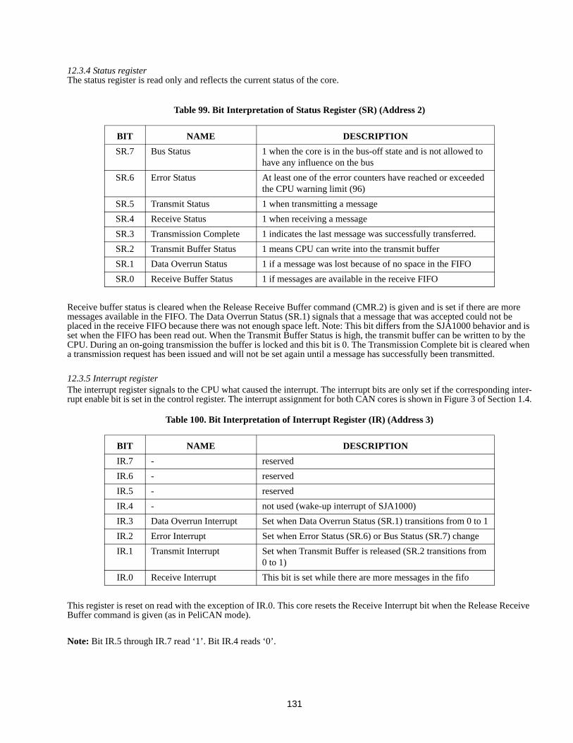
131
12.3.4 Status registerThe status register is read only and reflects the current status of the core.
Receive buffer status is cleared when the Release Receive Buffer command (CMR.2) is given and is set if there are more messages available in the FIFO. The Data Overrun Status (SR.1) signals that a message that was accepted could not be placed in the receive FIFO because there was not enough space left. Note: This bit differs from the SJA1000 behavior and is set when the FIFO has been read out. When the Transmit Buffer Status is high, the transmit buffer can be written to by the CPU. During an on-going transmission the buffer is locked and this bit is 0. The Transmission Complete bit is cleared when a transmission request has been issued and will not be set again until a message has successfully been transmitted.
12.3.5 Interrupt registerThe interrupt register signals to the CPU what caused the interrupt. The interrupt bits are only set if the corresponding inter-rupt enable bit is set in the control register. The interrupt assignment for both CAN cores is shown in Figure 3 of Section 1.4.
This register is reset on read with the exception of IR.0. This core resets the Receive Interrupt bit when the Release Receive Buffer command is given (as in PeliCAN mode).
Note: Bit IR.5 through IR.7 read ‘1’. Bit IR.4 reads ‘0’.
Table 99. Bit Interpretation of Status Register (SR) (Address 2)
BIT NAME DESCRIPTION
SR.7 Bus Status 1 when the core is in the bus-off state and is not allowed to have any influence on the bus
SR.6 Error Status At least one of the error counters have reached or exceeded the CPU warning limit (96)
SR.5 Transmit Status 1 when transmitting a message
SR.4 Receive Status 1 when receiving a message
SR.3 Transmission Complete 1 indicates the last message was successfully transferred.
SR.2 Transmit Buffer Status 1 means CPU can write into the transmit buffer
SR.1 Data Overrun Status 1 if a message was lost because of no space in the FIFO
SR.0 Receive Buffer Status 1 if messages are available in the receive FIFO
Table 100. Bit Interpretation of Interrupt Register (IR) (Address 3)
BIT NAME DESCRIPTION
IR.7 - reserved
IR.6 - reserved
IR.5 - reserved
IR.4 - not used (wake-up interrupt of SJA1000)
IR.3 Data Overrun Interrupt Set when Data Overrun Status (SR.1) transitions from 0 to 1
IR.2 Error Interrupt Set when Error Status (SR.6) or Bus Status (SR.7) change
IR.1 Transmit Interrupt Set when Transmit Buffer is released (SR.2 transitions from 0 to 1)
IR.0 Receive Interrupt This bit is set while there are more messages in the fifo
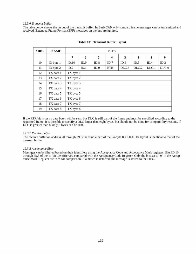
132
12.3.6 Transmit bufferThe table below shows the layout of the transmit buffer. In BasicCAN only standard frame messages can be transmitted and received. Extended Frame Format (EFF) messages on the bus are ignored.
If the RTR bit is set no data bytes will be sent, but DLC is still part of the frame and must be specified according to the requested frame. It is possible to specify a DLC larger than eight bytes, but should not be done for compatibility reasons. If DLC is greater than 8, only 8 bytes can be sent.
12.3.7 Receive bufferThe receive buffer on address 20 through 29 is the visible part of the 64-byte RX FIFO. Its layout is identical to that of the transmit buffer.
12.3.8 Acceptance filterMessages can be filtered based on their identifiers using the Acceptance Code and Acceptance Mask registers. Bits ID.10 through ID.3 of the 11-bit identifier are compared with the Acceptance Code Register. Only the bits set to ‘0’ in the Accep-tance Mask Register are used for comparison. If a match is detected, the message is stored to the FIFO.
Table 101. Transmit Buffer Layout
ADDR NAME BITS
7 6 5 4 3 2 1 0
10 ID byte 1 ID.10 ID.9 ID.8 ID.7 ID.6 ID.5 ID.4 ID.3
11 ID byte 2 ID.2 ID.1 ID.0 RTR DLC.3 DLC.2 DLC.1 DLC.0
12 TX data 1 TX byte 1
13 TX data 2 TX byte 2
14 TX data 3 TX byte 3
15 TX data 4 TX byte 4
16 TX data 5 TX byte 5
17 TX data 6 TX byte 6
18 TX data 7 TX byte 7
19 TX data 8 TX byte 8
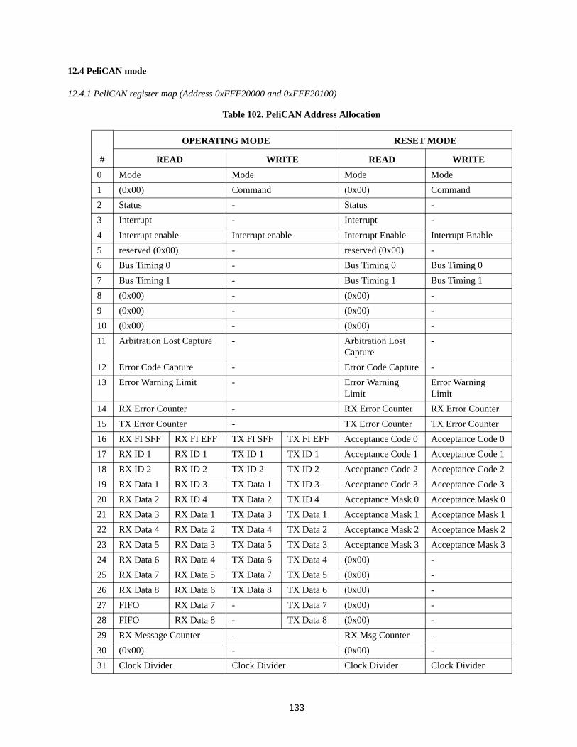
133
12.4 PeliCAN mode
12.4.1 PeliCAN register map (Address 0xFFF20000 and 0xFFF20100)
Table 102. PeliCAN Address Allocation
#
OPERATING MODE RESET MODE
READ WRITE READ WRITE
0 Mode Mode Mode Mode
1 (0x00) Command (0x00) Command
2 Status - Status -
3 Interrupt - Interrupt -
4 Interrupt enable Interrupt enable Interrupt Enable Interrupt Enable
5 reserved (0x00) - reserved (0x00) -
6 Bus Timing 0 - Bus Timing 0 Bus Timing 0
7 Bus Timing 1 - Bus Timing 1 Bus Timing 1
8 (0x00) - (0x00) -
9 (0x00) - (0x00) -
10 (0x00) - (0x00) -
11 Arbitration Lost Capture - Arbitration Lost Capture
-
12 Error Code Capture - Error Code Capture -
13 Error Warning Limit - Error Warning Limit
Error Warning Limit
14 RX Error Counter - RX Error Counter RX Error Counter
15 TX Error Counter - TX Error Counter TX Error Counter
16 RX FI SFF RX FI EFF TX FI SFF TX FI EFF Acceptance Code 0 Acceptance Code 0
17 RX ID 1 RX ID 1 TX ID 1 TX ID 1 Acceptance Code 1 Acceptance Code 1
18 RX ID 2 RX ID 2 TX ID 2 TX ID 2 Acceptance Code 2 Acceptance Code 2
19 RX Data 1 RX ID 3 TX Data 1 TX ID 3 Acceptance Code 3 Acceptance Code 3
20 RX Data 2 RX ID 4 TX Data 2 TX ID 4 Acceptance Mask 0 Acceptance Mask 0
21 RX Data 3 RX Data 1 TX Data 3 TX Data 1 Acceptance Mask 1 Acceptance Mask 1
22 RX Data 4 RX Data 2 TX Data 4 TX Data 2 Acceptance Mask 2 Acceptance Mask 2
23 RX Data 5 RX Data 3 TX Data 5 TX Data 3 Acceptance Mask 3 Acceptance Mask 3
24 RX Data 6 RX Data 4 TX Data 6 TX Data 4 (0x00) -
25 RX Data 7 RX Data 5 TX Data 7 TX Data 5 (0x00) -
26 RX Data 8 RX Data 6 TX Data 8 TX Data 6 (0x00) -
27 FIFO RX Data 7 - TX Data 7 (0x00) -
28 FIFO RX Data 8 - TX Data 8 (0x00) -
29 RX Message Counter - RX Msg Counter -
30 (0x00) - (0x00) -
31 Clock Divider Clock Divider Clock Divider Clock Divider
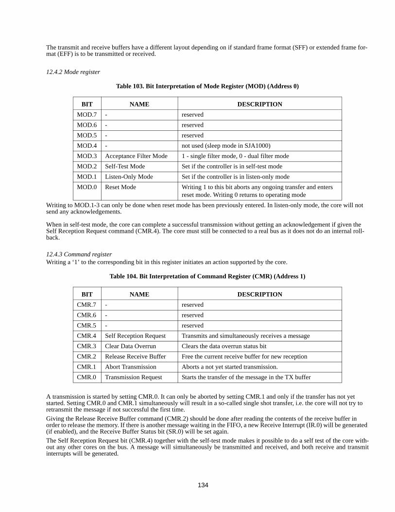
134
The transmit and receive buffers have a different layout depending on if standard frame format (SFF) or extended frame for-mat (EFF) is to be transmitted or received.
12.4.2 Mode register
Writing to MOD.1-3 can only be done when reset mode has been previously entered. In listen-only mode, the core will not send any acknowledgements.
When in self-test mode, the core can complete a successful transmission without getting an acknowledgement if given the Self Reception Request command (CMR.4). The core must still be connected to a real bus as it does not do an internal roll-back.
12.4.3 Command registerWriting a ‘1’ to the corresponding bit in this register initiates an action supported by the core.
A transmission is started by setting CMR.0. It can only be aborted by setting CMR.1 and only if the transfer has not yet started. Setting CMR.0 and CMR.1 simultaneously will result in a so-called single shot transfer, i.e. the core will not try to retransmit the message if not successful the first time.
Giving the Release Receive Buffer command (CMR.2) should be done after reading the contents of the receive buffer in order to release the memory. If there is another message waiting in the FIFO, a new Receive Interrupt (IR.0) will be generated (if enabled), and the Receive Buffer Status bit (SR.0) will be set again.
The Self Reception Request bit (CMR.4) together with the self-test mode makes it possible to do a self test of the core with-out any other cores on the bus. A message will simultaneously be transmitted and received, and both receive and transmitinterrupts will be generated.
Table 103. Bit Interpretation of Mode Register (MOD) (Address 0)
BIT NAME DESCRIPTION
MOD.7 - reserved
MOD.6 - reserved
MOD.5 - reserved
MOD.4 - not used (sleep mode in SJA1000)
MOD.3 Acceptance Filter Mode 1 - single filter mode, 0 - dual filter mode
MOD.2 Self-Test Mode Set if the controller is in self-test mode
MOD.1 Listen-Only Mode Set if the controller is in listen-only mode
MOD.0 Reset Mode Writing 1 to this bit aborts any ongoing transfer and enters reset mode. Writing 0 returns to operating mode
Table 104. Bit Interpretation of Command Register (CMR) (Address 1)
BIT NAME DESCRIPTION
CMR.7 - reserved
CMR.6 - reserved
CMR.5 - reserved
CMR.4 Self Reception Request Transmits and simultaneously receives a message
CMR.3 Clear Data Overrun Clears the data overrun status bit
CMR.2 Release Receive Buffer Free the current receive buffer for new reception
CMR.1 Abort Transmission Aborts a not yet started transmission.
CMR.0 Transmission Request Starts the transfer of the message in the TX buffer
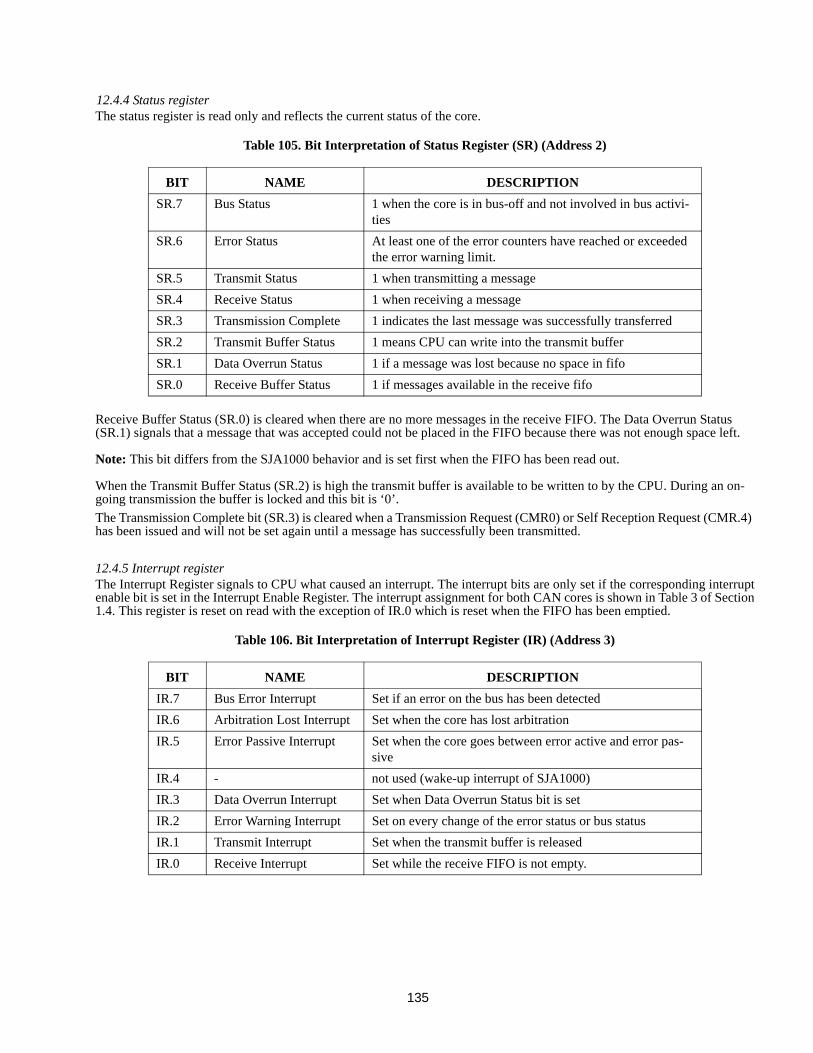
135
12.4.4 Status registerThe status register is read only and reflects the current status of the core.
Receive Buffer Status (SR.0) is cleared when there are no more messages in the receive FIFO. The Data Overrun Status (SR.1) signals that a message that was accepted could not be placed in the FIFO because there was not enough space left.
Note: This bit differs from the SJA1000 behavior and is set first when the FIFO has been read out.
When the Transmit Buffer Status (SR.2) is high the transmit buffer is available to be written to by the CPU. During an on-going transmission the buffer is locked and this bit is ‘0’.
The Transmission Complete bit (SR.3) is cleared when a Transmission Request (CMR0) or Self Reception Request (CMR.4) has been issued and will not be set again until a message has successfully been transmitted.
12.4.5 Interrupt registerThe Interrupt Register signals to CPU what caused an interrupt. The interrupt bits are only set if the corresponding interruptenable bit is set in the Interrupt Enable Register. The interrupt assignment for both CAN cores is shown in Table 3 of Section1.4. This register is reset on read with the exception of IR.0 which is reset when the FIFO has been emptied.
Table 105. Bit Interpretation of Status Register (SR) (Address 2)
BIT NAME DESCRIPTION
SR.7 Bus Status 1 when the core is in bus-off and not involved in bus activi-ties
SR.6 Error Status At least one of the error counters have reached or exceeded the error warning limit.
SR.5 Transmit Status 1 when transmitting a message
SR.4 Receive Status 1 when receiving a message
SR.3 Transmission Complete 1 indicates the last message was successfully transferred
SR.2 Transmit Buffer Status 1 means CPU can write into the transmit buffer
SR.1 Data Overrun Status 1 if a message was lost because no space in fifo
SR.0 Receive Buffer Status 1 if messages available in the receive fifo
Table 106. Bit Interpretation of Interrupt Register (IR) (Address 3)
BIT NAME DESCRIPTION
IR.7 Bus Error Interrupt Set if an error on the bus has been detected
IR.6 Arbitration Lost Interrupt Set when the core has lost arbitration
IR.5 Error Passive Interrupt Set when the core goes between error active and error pas-sive
IR.4 - not used (wake-up interrupt of SJA1000)
IR.3 Data Overrun Interrupt Set when Data Overrun Status bit is set
IR.2 Error Warning Interrupt Set on every change of the error status or bus status
IR.1 Transmit Interrupt Set when the transmit buffer is released
IR.0 Receive Interrupt Set while the receive FIFO is not empty.
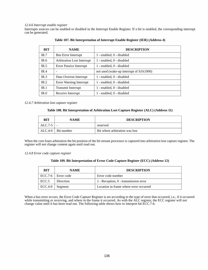
136
12.4.6 Interrupt enable registerInterrupts sources can be enabled or disabled in the Interrupt Enable Register. If a bit is enabled, the corresponding interruptcan be generated.
12.4.7 Arbitration lost capture register
When the core loses arbitration the bit position of the bit stream processor is captured into arbitration lost capture register. The register will not change content again until read out.
12.4.8 Error code capture register
When a bus error occurs, the Error Code Capture Register is set according to the type of error that occurred, i.e., if it occurred while transmitting or receiving, and where in the frame it occurred. As with the ALC register, the ECC register will not change value until it has been read out. The following table shows how to interpret bit ECC.7-6.
Table 107. Bit Interpretation of Interrupt Enable Register (IER) (Address 4)
BIT NAME DESCRIPTION
IR.7 Bus Error Interrupt 1 - enabled, 0 - disabled
IR.6 Arbitration Lost Interrupt 1 - enabled, 0 - disabled
IR.5 Error Passive Interrupt 1 - enabled, 0 - disabled
IR.4 - not used (wake-up interrupt of SJA1000)
IR.3 Data Overrun Interrupt 1 - enabled, 0 - disabled
IR.2 Error Warning Interrupt 1 - enabled, 0 - disabled.
IR.1 Transmit Interrupt 1 - enabled, 0 - disabled
IR.0 Receive Interrupt 1 - enabled, 0 - disabled
Table 108. Bit Interpretation of Arbitration Lost Capture Register (ALC) (Address 11)
BIT NAME DESCRIPTION
ALC.7-5 - reserved
ALC.4-0 Bit number Bit where arbitration was lost
Table 109. Bit Interpretation of Error Code Capture Register (ECC) (Address 12)
BIT NAME DESCRIPTION
ECC.7-6 Error code Error code number
ECC.5 Direction 1 - Reception, 0 - transmission error
ECC.4-0 Segment Location in frame where error occurred
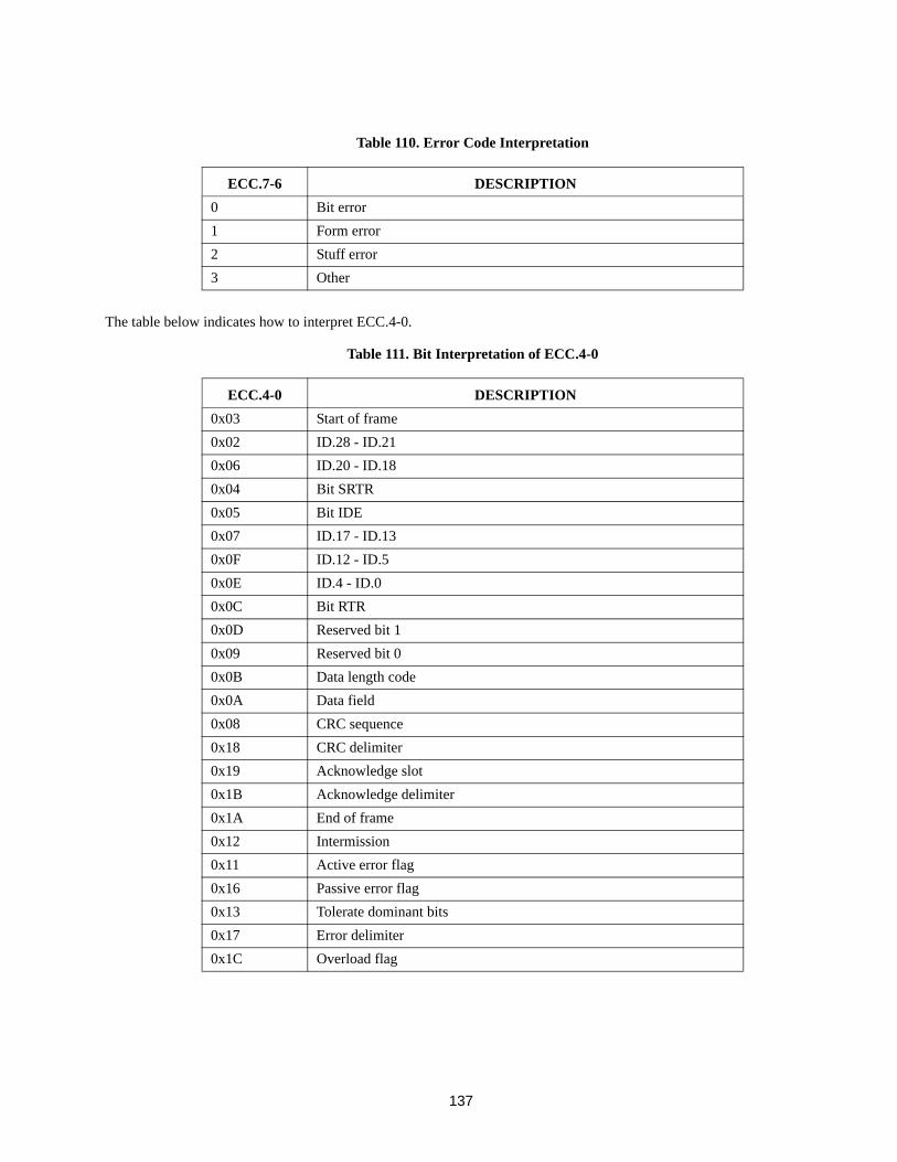
137
The table below indicates how to interpret ECC.4-0.
Table 110. Error Code Interpretation
ECC.7-6 DESCRIPTION
0 Bit error
1 Form error
2 Stuff error
3 Other
Table 111. Bit Interpretation of ECC.4-0
ECC.4-0 DESCRIPTION
0x03 Start of frame
0x02 ID.28 - ID.21
0x06 ID.20 - ID.18
0x04 Bit SRTR
0x05 Bit IDE
0x07 ID.17 - ID.13
0x0F ID.12 - ID.5
0x0E ID.4 - ID.0
0x0C Bit RTR
0x0D Reserved bit 1
0x09 Reserved bit 0
0x0B Data length code
0x0A Data field
0x08 CRC sequence
0x18 CRC delimiter
0x19 Acknowledge slot
0x1B Acknowledge delimiter
0x1A End of frame
0x12 Intermission
0x11 Active error flag
0x16 Passive error flag
0x13 Tolerate dominant bits
0x17 Error delimiter
0x1C Overload flag
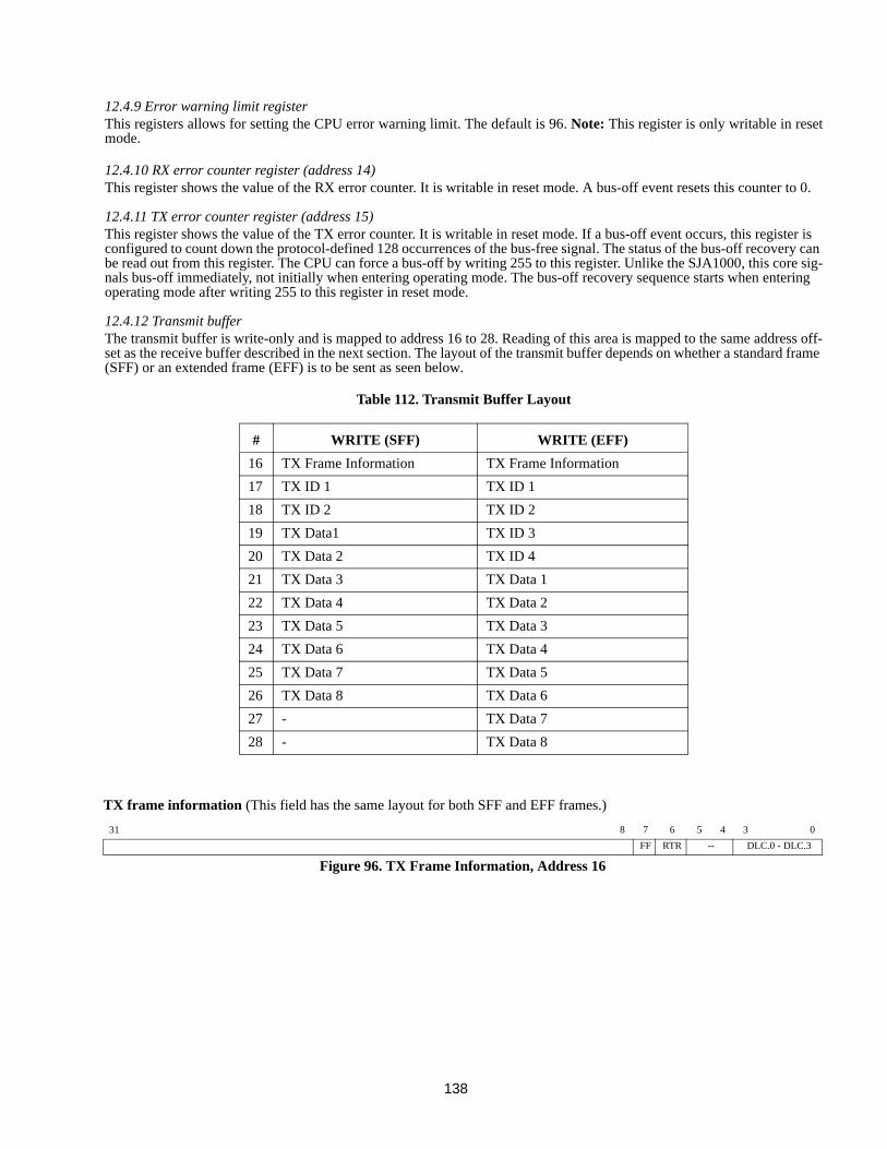
138
12.4.9 Error warning limit registerThis registers allows for setting the CPU error warning limit. The default is 96. Note: This register is only writable in resetmode.
12.4.10 RX error counter register (address 14)This register shows the value of the RX error counter. It is writable in reset mode. A bus-off event resets this counter to 0.
12.4.11 TX error counter register (address 15)This register shows the value of the TX error counter. It is writable in reset mode. If a bus-off event occurs, this register is configured to count down the protocol-defined 128 occurrences of the bus-free signal. The status of the bus-off recovery can be read out from this register. The CPU can force a bus-off by writing 255 to this register. Unlike the SJA1000, this core sig-nals bus-off immediately, not initially when entering operating mode. The bus-off recovery sequence starts when entering operating mode after writing 255 to this register in reset mode.
12.4.12 Transmit bufferThe transmit buffer is write-only and is mapped to address 16 to 28. Reading of this area is mapped to the same address off-set as the receive buffer described in the next section. The layout of the transmit buffer depends on whether a standard frame (SFF) or an extended frame (EFF) is to be sent as seen below.
Table 112. Transmit Buffer Layout
# WRITE (SFF) WRITE (EFF)
16 TX Frame Information TX Frame Information
17 TX ID 1 TX ID 1
18 TX ID 2 TX ID 2
19 TX Data1 TX ID 3
20 TX Data 2 TX ID 4
21 TX Data 3 TX Data 1
22 TX Data 4 TX Data 2
23 TX Data 5 TX Data 3
24 TX Data 6 TX Data 4
25 TX Data 7 TX Data 5
26 TX Data 8 TX Data 6
27 - TX Data 7
28 - TX Data 8
TX frame information (This field has the same layout for both SFF and EFF frames.)
31 8 7 6 5 4 3 0
FF RTR -- DLC.0 - DLC.3
Figure 96. TX Frame Information, Address 16
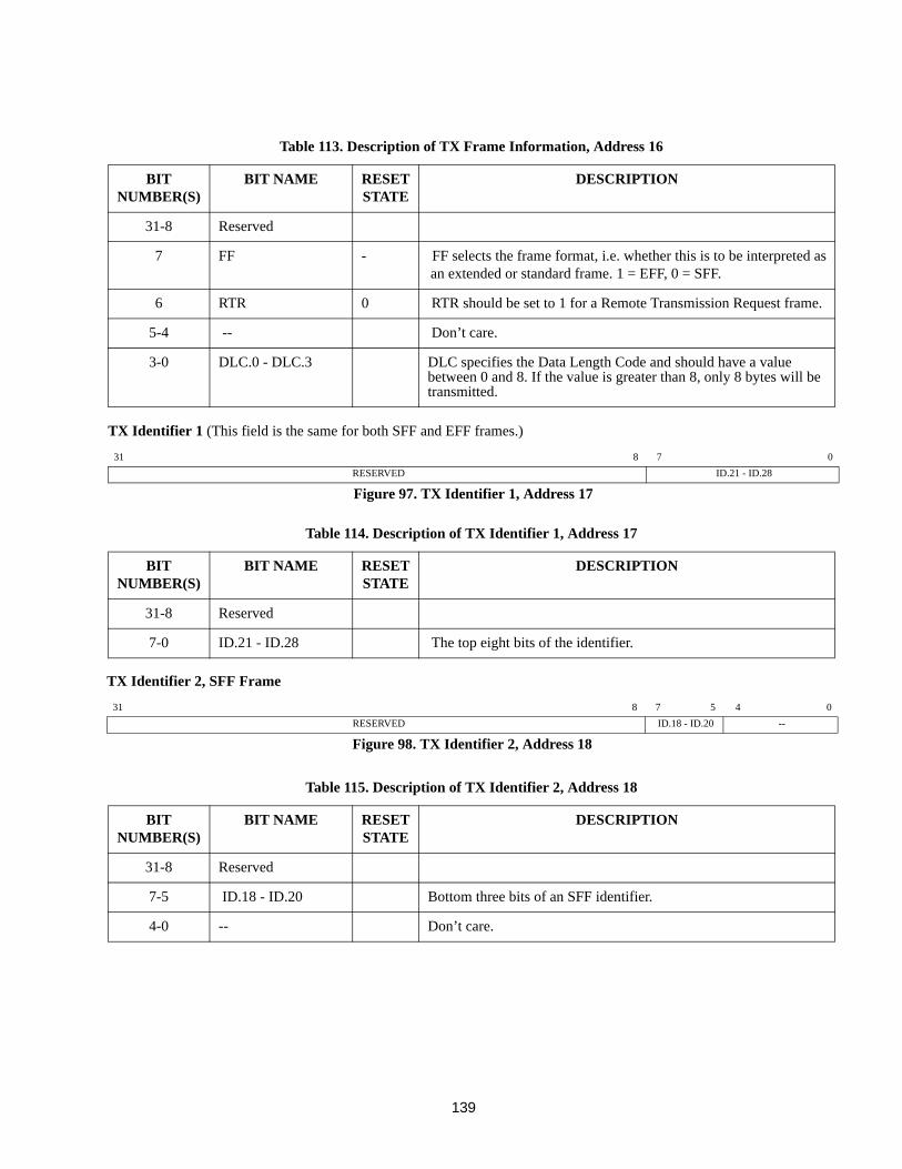
139
Table 113. Description of TX Frame Information, Address 16
BIT NUMBER(S)
BIT NAME RESET STATE
DESCRIPTION
31-8 Reserved
7 FF - FF selects the frame format, i.e. whether this is to be interpreted asan extended or standard frame. 1 = EFF, 0 = SFF.
6 RTR 0 RTR should be set to 1 for a Remote Transmission Request frame.
5-4 -- Don’t care.
3-0 DLC.0 - DLC.3 DLC specifies the Data Length Code and should have a value between 0 and 8. If the value is greater than 8, only 8 bytes will be transmitted.
Table 114. Description of TX Identifier 1, Address 17
BIT NUMBER(S)
BIT NAME RESET STATE
DESCRIPTION
31-8 Reserved
7-0 ID.21 - ID.28 The top eight bits of the identifier.
Table 115. Description of TX Identifier 2, Address 18
BIT NUMBER(S)
BIT NAME RESET STATE
DESCRIPTION
31-8 Reserved
7-5 ID.18 - ID.20 Bottom three bits of an SFF identifier.
4-0 -- Don’t care.
TX Identifier 1 (This field is the same for both SFF and EFF frames.)
31 8 7 0
RESERVED ID.21 - ID.28
Figure 97. TX Identifier 1, Address 17
TX Identifier 2, SFF Frame
31 8 7 5 4 0
RESERVED ID.18 - ID.20 --
Figure 98. TX Identifier 2, Address 18
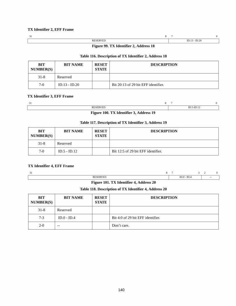
140
Table 116. Description of TX Identifier 2, Address 18
BIT NUMBER(S)
BIT NAME RESET STATE
DESCRIPTION
31-8 Reserved
7-0 ID.13 - ID.20 Bit 20:13 of 29 bit EFF identifier.
Table 117. Description of TX Identifier 3, Address 19
BIT NUMBER(S)
BIT NAME RESET STATE
DESCRIPTION
31-8 Reserved
7-0 ID.5 - ID.12 Bit 12:5 of 29 bit EFF identifier.
Table 118. Description of TX Identifier 4, Address 20
BIT NUMBER(S)
BIT NAME RESET STATE
DESCRIPTION
31-8 Reserved
7-3 ID.0 - ID.4 Bit 4:0 of 29 bit EFF identifier.
2-0 -- Don’t care.
TX Identifier 2, EFF Frame
31 8 7 0
RESERVED ID.13 - ID.20
Figure 99. TX Identifier 2, Address 18
TX Identifier 3, EFF Frame
31 8 7 0
RESERVED ID.5-ID.12
Figure 100. TX Identifier 3, Address 19
TX Identifier 4, EFF Frame
31 8 7 3 2 0
RESERVED ID.0 - ID.4 --
Figure 101. TX Identifier 4, Address 20
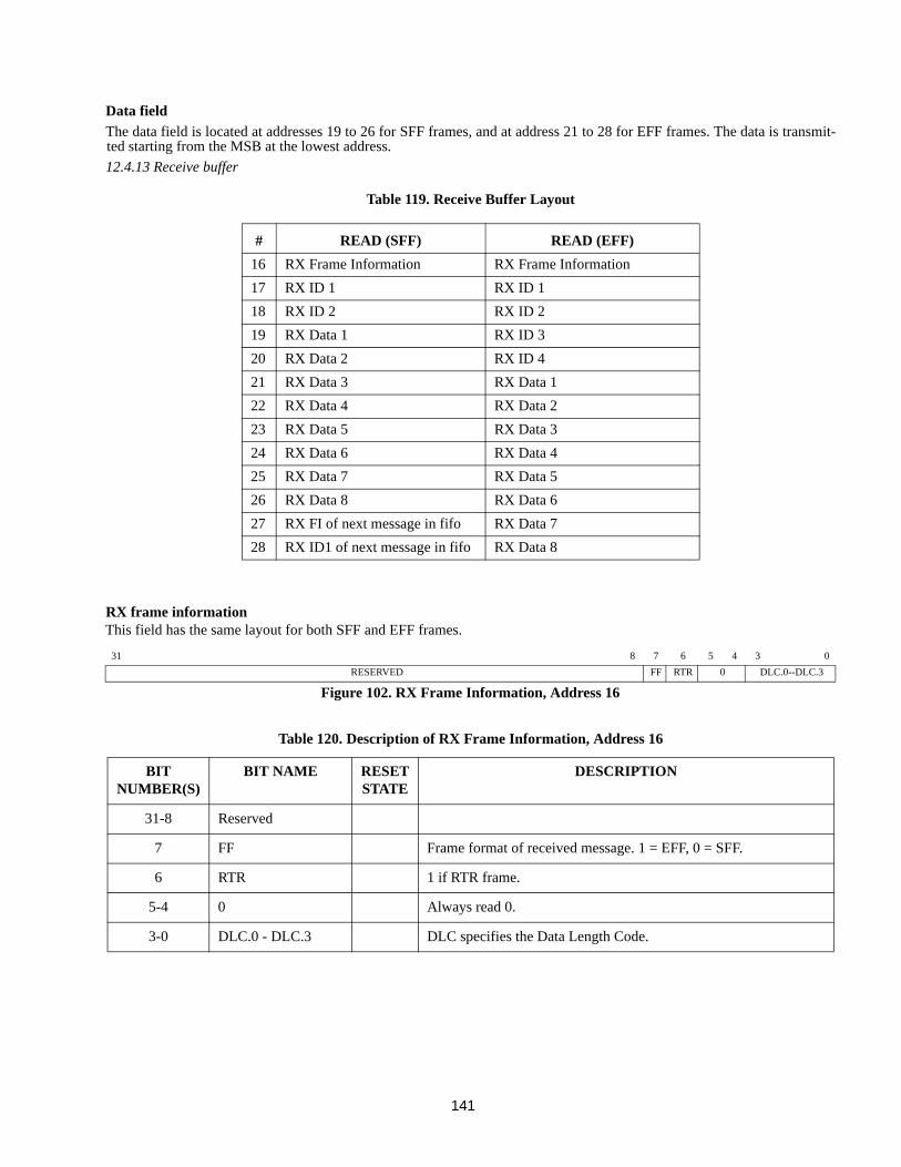
141
Data field
The data field is located at addresses 19 to 26 for SFF frames, and at address 21 to 28 for EFF frames. The data is transmit-ted starting from the MSB at the lowest address.
12.4.13 Receive buffer
RX frame information
Table 119. Receive Buffer Layout
# READ (SFF) READ (EFF)
16 RX Frame Information RX Frame Information
17 RX ID 1 RX ID 1
18 RX ID 2 RX ID 2
19 RX Data 1 RX ID 3
20 RX Data 2 RX ID 4
21 RX Data 3 RX Data 1
22 RX Data 4 RX Data 2
23 RX Data 5 RX Data 3
24 RX Data 6 RX Data 4
25 RX Data 7 RX Data 5
26 RX Data 8 RX Data 6
27 RX FI of next message in fifo RX Data 7
28 RX ID1 of next message in fifo RX Data 8
Table 120. Description of RX Frame Information, Address 16
BIT NUMBER(S)
BIT NAME RESET STATE
DESCRIPTION
31-8 Reserved
7 FF Frame format of received message. 1 = EFF, 0 = SFF.
6 RTR 1 if RTR frame.
5-4 0 Always read 0.
3-0 DLC.0 - DLC.3 DLC specifies the Data Length Code.
This field has the same layout for both SFF and EFF frames.
31 8 7 6 5 4 3 0
RESERVED FF RTR 0 DLC.0--DLC.3
Figure 102. RX Frame Information, Address 16
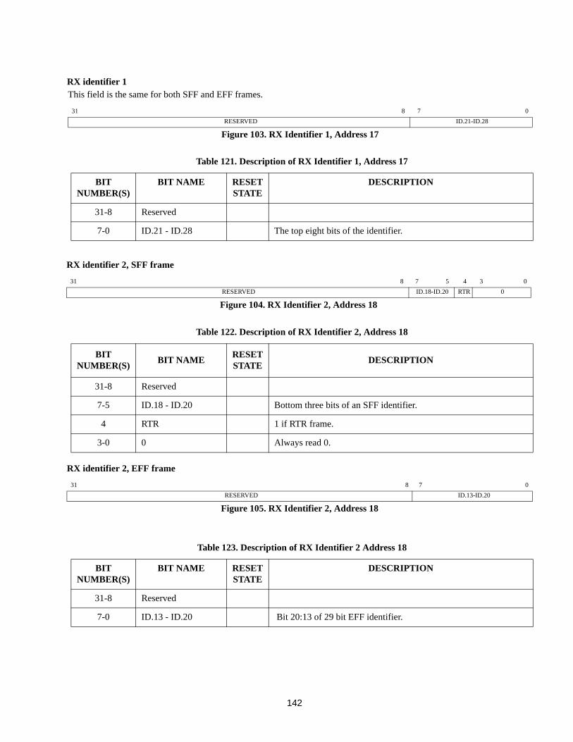
142
RX identifier 1
Table 121. Description of RX Identifier 1, Address 17
BIT NUMBER(S)
BIT NAME RESET STATE
DESCRIPTION
31-8 Reserved
7-0 ID.21 - ID.28 The top eight bits of the identifier.
Table 122. Description of RX Identifier 2, Address 18
BIT NUMBER(S)
BIT NAMERESET STATE
DESCRIPTION
31-8 Reserved
7-5 ID.18 - ID.20 Bottom three bits of an SFF identifier.
4 RTR 1 if RTR frame.
3-0 0 Always read 0.
Table 123. Description of RX Identifier 2 Address 18
BIT NUMBER(S)
BIT NAME RESET STATE
DESCRIPTION
31-8 Reserved
7-0 ID.13 - ID.20 Bit 20:13 of 29 bit EFF identifier.
RX identifier 2, SFF frame
31 8 7 5 4 3 0
RESERVED ID.18-ID.20 RTR 0
Figure 104. RX Identifier 2, Address 18
This field is the same for both SFF and EFF frames.
31 8 7 0
RESERVED ID.21-ID.28
Figure 103. RX Identifier 1, Address 17
RX identifier 2, EFF frame
31 8 7 0
RESERVED ID.13-ID.20
Figure 105. RX Identifier 2, Address 18
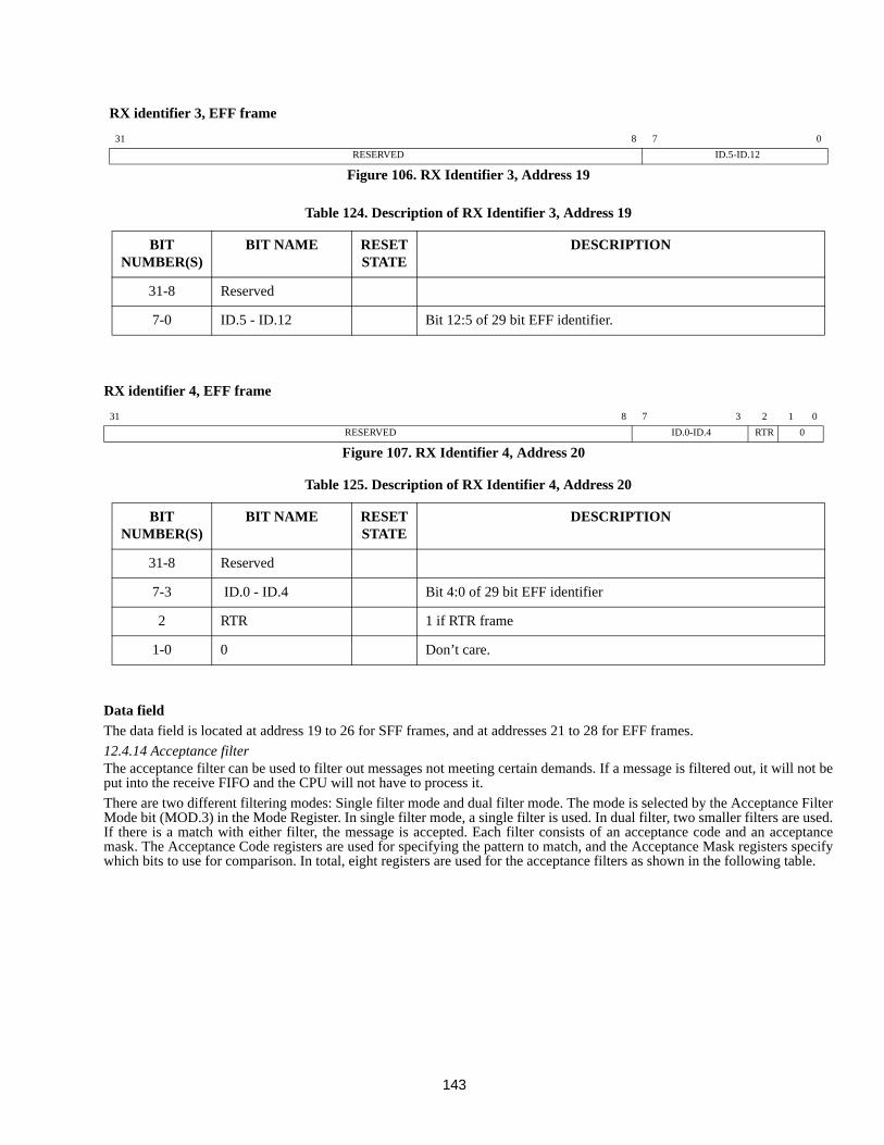
143
Data field
The data field is located at address 19 to 26 for SFF frames, and at addresses 21 to 28 for EFF frames.
12.4.14 Acceptance filterThe acceptance filter can be used to filter out messages not meeting certain demands. If a message is filtered out, it will not beput into the receive FIFO and the CPU will not have to process it.
There are two different filtering modes: Single filter mode and dual filter mode. The mode is selected by the Acceptance FilterMode bit (MOD.3) in the Mode Register. In single filter mode, a single filter is used. In dual filter, two smaller filters are used.If there is a match with either filter, the message is accepted. Each filter consists of an acceptance code and an acceptancemask. The Acceptance Code registers are used for specifying the pattern to match, and the Acceptance Mask registers specifywhich bits to use for comparison. In total, eight registers are used for the acceptance filters as shown in the following table.
Table 124. Description of RX Identifier 3, Address 19
BIT NUMBER(S)
BIT NAME RESET STATE
DESCRIPTION
31-8 Reserved
7-0 ID.5 - ID.12 Bit 12:5 of 29 bit EFF identifier.
Table 125. Description of RX Identifier 4, Address 20
BIT NUMBER(S)
BIT NAME RESET STATE
DESCRIPTION
31-8 Reserved
7-3 ID.0 - ID.4 Bit 4:0 of 29 bit EFF identifier
2 RTR 1 if RTR frame
1-0 0 Don’t care.
RX identifier 3, EFF frame
31 8 7 0
RESERVED ID.5-ID.12
Figure 106. RX Identifier 3, Address 19
RX identifier 4, EFF frame
31 8 7 3 2 1 0
RESERVED ID.0-ID.4 RTR 0
Figure 107. RX Identifier 4, Address 20
144
Note: The registers are only read/writable in reset mode.
Single filter mode, standard frame
When receiving a standard frame in single filter mode the registers ACR0-3 are compared against the incoming message inthe following way:
ACR0.7-0 & ACR1.7-5 are compared to ID.28-18
ACR1.4 is compared to the RTR bit.
ACR1.3-0 are unused.
ACR2 & ACR3 are compared to data byte 1 & 2.
The corresponding bits in the AMR registers select which bits are used for comparison. A set bit in the mask register meansdon’t care.
Single filter mode, extended frame
When receiving an extended frame in single filter mode the registers ACR0-3 are compared against the incoming message inthe following way:
ACR0.7-0 & ACR1.7-0 are compared to ID.28-13
ACR2.7-0 & ACR3.7-3 are compared to ID.12-0
ACR3.2 are compared to the RTR bit
ACR3.1-0 are unused.
The corresponding bits in the AMR registers select which bits are used for comparison. A set bit in the mask register meansdon’t care.
Dual filter mode, standard frame
When receiving a standard frame in dual filter mode the registers ACR0-3 are compared against the incoming message in thefollowing way:
Filter 1
ACR0.7-0 & ACR1.7-5 are compared to ID.28-18
ACR1.4 is compared to the RTR bit.
ACR1.3-0 are compared against upper nibble of data byte 1
ACR3.3-0 are compared against lower nibble of data byte 1
Table 126. Acceptance Filter Registers
ADDRESS DESCRIPTION
16 Acceptance Code 0 (ACR0)
17 Acceptance Code 1 (ACR1)
18 Acceptance Code 2 (ACR2)
19 Acceptance Code 3 (ACR3)
20 Acceptance Mask 0 (AMR0)
21 Acceptance Mask 1 (AMR1)
22 Acceptance Mask 2 (AMR2)
23 Acceptance Mask 3 (AMR3)
145
Filter 2
ACR2.7-0 & ACR3.7-5 are compared to ID.28-18
ACR3.4 is compared to the RTR bit.
The corresponding bits in the AMR registers select which bits are used for comparison. A set bit in the mask register meansdon’t care.
Dual filter mode, extended frame
When receiving a standard frame in dual filter mode the registers ACR0-3 are compared against the incoming message in thefollowing way:
Filter 1
ACR0.7-0 & ACR1.7-0 are compared to ID.28-13
Filter 2
ACR2.7-0 & ACR3.7-0 are compared to ID.28-13
The corresponding bits in the AMR registers select which bits are used for comparison. A set bit in the mask register meansdon’t care.
12.4.15 RX Message CounterThe RX message counter register at address 29 holds the number of messages currently stored in the receive FIFO. The topthree bits are always 0.
12.5 Common registersThere are three common registers that are at the same addresses and have the same functionality in both BasiCAN and PeliCAN mode. These are the Clock Divider Register and Bit Timing Registers 0 and 1.
12.5.1 Clock Divider RegisterThe only function of this register in the GRLIB version of the Opencores CAN is to choose between PeliCAN and BasiCAN.
Table 127. Bit Interpretation of Clock Divider Register (CDR) (Address 31)
BIT NAME DESCRIPTION
CDR.7 CAN mode 1 - PeliCAN, 0 - BasiCAN
CDR.6 - unused
CDR.5 - unused
CDR.4 - reserved
CDR.3 - reserved
CDR.2 - reserved
CDR.1 - reserved
CDR.0 - reserved
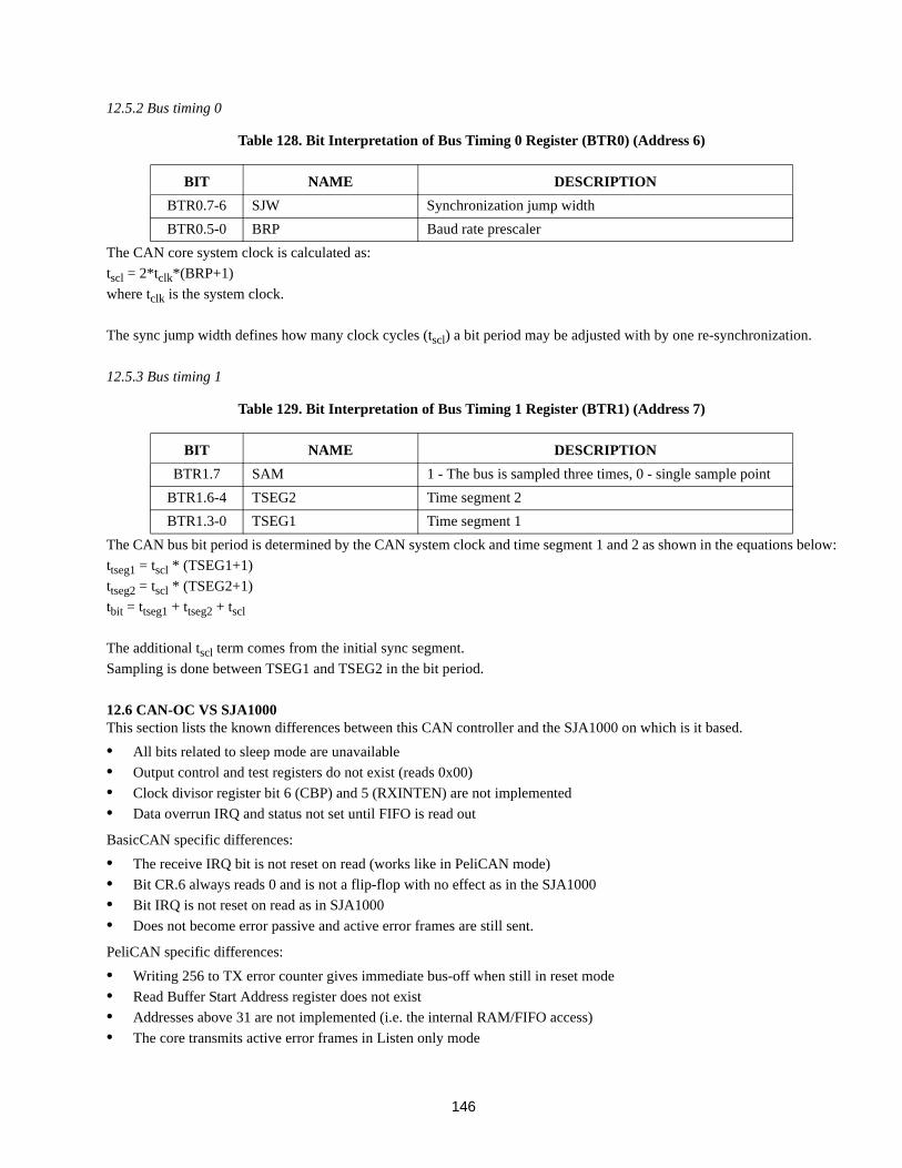
146
12.5.2 Bus timing 0
The CAN core system clock is calculated as:
tscl = 2*tclk*(BRP+1)
where tclk is the system clock.
The sync jump width defines how many clock cycles (tscl) a bit period may be adjusted with by one re-synchronization.
12.5.3 Bus timing 1
The CAN bus bit period is determined by the CAN system clock and time segment 1 and 2 as shown in the equations below:
ttseg1 = tscl * (TSEG1+1)
ttseg2 = tscl * (TSEG2+1)
tbit = ttseg1 + ttseg2 + tscl
The additional tscl term comes from the initial sync segment.
Sampling is done between TSEG1 and TSEG2 in the bit period.
12.6 CAN-OC VS SJA1000This section lists the known differences between this CAN controller and the SJA1000 on which is it based.
• All bits related to sleep mode are unavailable
• Output control and test registers do not exist (reads 0x00)
• Clock divisor register bit 6 (CBP) and 5 (RXINTEN) are not implemented
• Data overrun IRQ and status not set until FIFO is read out
BasicCAN specific differences:
• The receive IRQ bit is not reset on read (works like in PeliCAN mode)
• Bit CR.6 always reads 0 and is not a flip-flop with no effect as in the SJA1000
• Bit IRQ is not reset on read as in SJA1000
• Does not become error passive and active error frames are still sent.
PeliCAN specific differences:
• Writing 256 to TX error counter gives immediate bus-off when still in reset mode
• Read Buffer Start Address register does not exist
• Addresses above 31 are not implemented (i.e. the internal RAM/FIFO access)
• The core transmits active error frames in Listen only mode
Table 128. Bit Interpretation of Bus Timing 0 Register (BTR0) (Address 6)
BIT NAME DESCRIPTION
BTR0.7-6 SJW Synchronization jump width
BTR0.5-0 BRP Baud rate prescaler
Table 129. Bit Interpretation of Bus Timing 1 Register (BTR1) (Address 7)
BIT NAME DESCRIPTION
BTR1.7 SAM 1 - The bus is sampled three times, 0 - single sample point
BTR1.6-4 TSEG2 Time segment 2
BTR1.3-0 TSEG1 Time segment 1
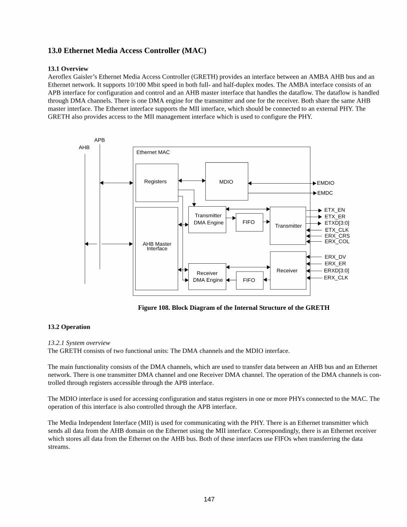
147
13.0 Ethernet Media Access Controller (MAC)
13.1 OverviewAeroflex Gaisler’s Ethernet Media Access Controller (GRETH) provides an interface between an AMBA AHB bus and an Ethernet network. It supports 10/100 Mbit speed in both full- and half-duplex modes. The AMBA interface consists of an APB interface for configuration and control and an AHB master interface that handles the dataflow. The dataflow is handled through DMA channels. There is one DMA engine for the transmitter and one for the receiver. Both share the same AHB master interface. The Ethernet interface supports the MII interface, which should be connected to an external PHY. The GRETH also provides access to the MII management interface which is used to configure the PHY.
13.2 Operation
13.2.1 System overviewThe GRETH consists of two functional units: The DMA channels and the MDIO interface.
The main functionality consists of the DMA channels, which are used to transfer data between an AHB bus and an Ethernet network. There is one transmitter DMA channel and one Receiver DMA channel. The operation of the DMA channels is con-trolled through registers accessible through the APB interface.
The MDIO interface is used for accessing configuration and status registers in one or more PHYs connected to the MAC. The operation of this interface is also controlled through the APB interface.
The Media Independent Interface (MII) is used for communicating with the PHY. There is an Ethernet transmitter which sends all data from the AHB domain on the Ethernet using the MII interface. Correspondingly, there is an Ethernet receiver which stores all data from the Ethernet on the AHB bus. Both of these interfaces use FIFOs when transferring the data streams.
AHBAPB
Ethernet MAC
Registers MDIO
EMDIO
EMDC
AHB MasterInterface
Transmitter
Receiver
Transmitter
Receiver
DMA Engine
DMA Engine
FIFO
FIFO
ETX_ENETX_ERETXD[3:0]ETX_CLKERX_CRSERX_COL
ERX_DVERX_ERERXD[3:0]ERX_CLK
Figure 108. Block Diagram of the Internal Structure of the GRETH
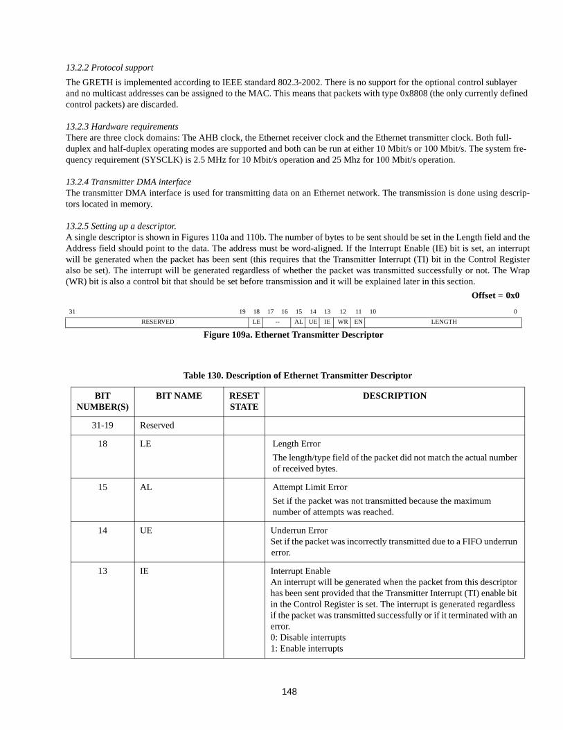
148
13.2.2 Protocol support
The GRETH is implemented according to IEEE standard 802.3-2002. There is no support for the optional control sublayer and no multicast addresses can be assigned to the MAC. This means that packets with type 0x8808 (the only currently defined control packets) are discarded.
13.2.3 Hardware requirementsThere are three clock domains: The AHB clock, the Ethernet receiver clock and the Ethernet transmitter clock. Both full-duplex and half-duplex operating modes are supported and both can be run at either 10 Mbit/s or 100 Mbit/s. The system fre-quency requirement (SYSCLK) is 2.5 MHz for 10 Mbit/s operation and 25 Mhz for 100 Mbit/s operation.
13.2.4 Transmitter DMA interfaceThe transmitter DMA interface is used for transmitting data on an Ethernet network. The transmission is done using descrip-tors located in memory.
13.2.5 Setting up a descriptor.A single descriptor is shown in Figures 110a and 110b. The number of bytes to be sent should be set in the Length field and theAddress field should point to the data. The address must be word-aligned. If the Interrupt Enable (IE) bit is set, an interruptwill be generated when the packet has been sent (this requires that the Transmitter Interrupt (TI) bit in the Control Registeralso be set). The interrupt will be generated regardless of whether the packet was transmitted successfully or not. The Wrap(WR) bit is also a control bit that should be set before transmission and it will be explained later in this section.
Table 130. Description of Ethernet Transmitter Descriptor
BIT NUMBER(S)
BIT NAME RESET STATE
DESCRIPTION
31-19 Reserved
18 LE Length Error
The length/type field of the packet did not match the actual number of received bytes.
15 AL Attempt Limit Error
Set if the packet was not transmitted because the maximum number of attempts was reached.
14 UE Underrun ErrorSet if the packet was incorrectly transmitted due to a FIFO underrun error.
13 IE Interrupt EnableAn interrupt will be generated when the packet from this descriptor has been sent provided that the Transmitter Interrupt (TI) enable bit in the Control Register is set. The interrupt is generated regardless if the packet was transmitted successfully or if it terminated with an error.0: Disable interrupts1: Enable interrupts
Offset = 0x0
31 19 18 17 16 15 14 13 12 11 10 0
RESERVED LE -- AL UE IE WR EN LENGTH
Figure 109a. Ethernet Transmitter Descriptor
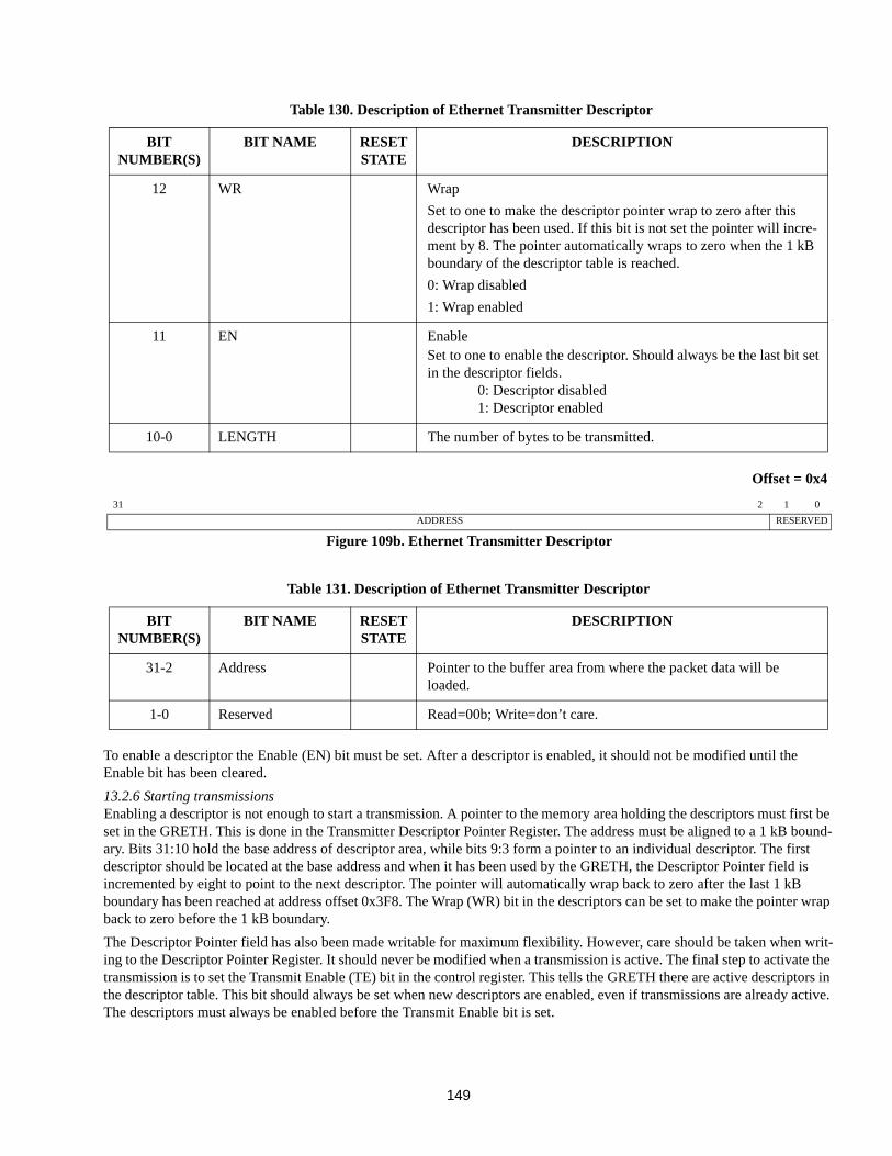
149
To enable a descriptor the Enable (EN) bit must be set. After a descriptor is enabled, it should not be modified until the Enable bit has been cleared.
13.2.6 Starting transmissionsEnabling a descriptor is not enough to start a transmission. A pointer to the memory area holding the descriptors must first be set in the GRETH. This is done in the Transmitter Descriptor Pointer Register. The address must be aligned to a 1 kB bound-ary. Bits 31:10 hold the base address of descriptor area, while bits 9:3 form a pointer to an individual descriptor. The first descriptor should be located at the base address and when it has been used by the GRETH, the Descriptor Pointer field is incremented by eight to point to the next descriptor. The pointer will automatically wrap back to zero after the last 1 kB boundary has been reached at address offset 0x3F8. The Wrap (WR) bit in the descriptors can be set to make the pointer wrap back to zero before the 1 kB boundary.
The Descriptor Pointer field has also been made writable for maximum flexibility. However, care should be taken when writ-ing to the Descriptor Pointer Register. It should never be modified when a transmission is active. The final step to activate the transmission is to set the Transmit Enable (TE) bit in the control register. This tells the GRETH there are active descriptors in the descriptor table. This bit should always be set when new descriptors are enabled, even if transmissions are already active. The descriptors must always be enabled before the Transmit Enable bit is set.
BIT NUMBER(S)
BIT NAME RESET STATE
DESCRIPTION
12 WR Wrap
Set to one to make the descriptor pointer wrap to zero after this descriptor has been used. If this bit is not set the pointer will incre-ment by 8. The pointer automatically wraps to zero when the 1 kB boundary of the descriptor table is reached.
0: Wrap disabled
1: Wrap enabled
11 EN EnableSet to one to enable the descriptor. Should always be the last bit setin the descriptor fields.
0: Descriptor disabled1: Descriptor enabled
10-0 LENGTH The number of bytes to be transmitted.
Table 131. Description of Ethernet Transmitter Descriptor
BIT NUMBER(S)
BIT NAME RESET STATE
DESCRIPTION
31-2 Address Pointer to the buffer area from where the packet data will be loaded.
1-0 Reserved Read=00b; Write=don’t care.
Table 130. Description of Ethernet Transmitter Descriptor
Offset = 0x4
31 2 1 0
ADDRESS RESERVED
Figure 109b. Ethernet Transmitter Descriptor
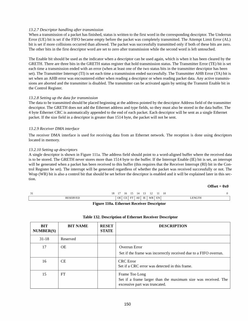
150
13.2.7 Descriptor handling after transmissionWhen a transmission of a packet has finished, status is written to the first word in the corresponding descriptor. The Underrun Error (UE) bit is set if the FIFO became empty before the packet was completely transmitted. The Attempt Limit Error (AL) bit is set if more collisions occurred than allowed. The packet was successfully transmitted only if both of these bits are zero. The other bits in the first descriptor word are set to zero after transmission while the second word is left untouched.
The Enable bit should be used as the indicator when a descriptor can be used again, which is when it has been cleared by the GRETH. There are three bits in the GRETH status register that hold transmission status. The Transmitter Error (TE) bit is set each time a transmission ended with an error (when at least one of the two status bits in the transmitter descriptor has been set). The Transmitter Interrupt (TI) is set each time a transmission ended successfully. The Transmitter AHB Error (TA) bit is set when an AHB error was encountered either when reading a descriptor or when reading packet data. Any active transmis-sions are aborted and the transmitter is disabled. The transmitter can be activated again by setting the Transmit Enable bit in the Control Register.
13.2.8 Setting up the data for transmissionThe data to be transmitted should be placed beginning at the address pointed by the descriptor Address field of the transmitter descriptor. The GRETH does not add the Ethernet address and type fields, so they must also be stored in the data buffer. The 4 byte Ethernet CRC is automatically appended to the end of each packet. Each descriptor will be sent as a single Ethernet packet. If the size field in a descriptor is greater than 1514 byte, the packet will not be sent.
13.2.9 Receiver DMA interface
The receiver DMA interface is used for receiving data from an Ethernet network. The reception is done using descriptorslocated in memory.
13.2.10 Setting up descriptorsA single descriptor is shown in Figure 111a. The address field should point to a word-aligned buffer where the received datais to be stored. The GRETH never stores more than 1514 byte to the buffer. If the Interrupt Enable (IE) bit is set, an interruptwill be generated when a packet has been received to this buffer (this requires that the Receiver Interrupt (RI) bit in the Con-trol Register be set). The interrupt will be generated regardless of whether the packet was received successfully or not. TheWrap (WR) bit is also a control bit that should be set before the descriptor is enabled and it will be explained later in this sec-tion.
Table 132. Description of Ethernet Receiver Descriptor
BIT NUMBER(S)
BIT NAME RESET STATE
DESCRIPTION
31-18 Reserved
17 OE Overrun Error
Set if the frame was incorrectly received due to a FIFO overrun.
16 CE CRC ErrorSet if a CRC error was detected in this frame.
15 FT Frame Too LongSet if a frame larger than the maximum size was received. Theexcessive part was truncated.
Offset = 0x0
31 18 17 16 15 14 13 12 11 10 0
RESERVED OE CE FT AE IE WR EN LENGTH
Figure 110a. Ethernet Receiver Descriptor
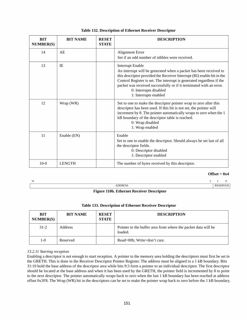
151
13.2.11 Starting receptionEnabling a descriptor is not enough to start reception. A pointer to the memory area holding the descriptors must first be set in the GRETH. This is done in the Receiver Descriptor Pointer Register. The address must be aligned to a 1 kB boundary. Bits 31:10 hold the base address of the descriptor area while bits 9:3 form a pointer to an individual descriptor. The first descriptor should be located at the base address and when it has been used by the GRETH, the pointer field is incremented by 8 to point to the next descriptor. The pointer automatically wraps back to zero when the last 1 kB boundary has been reached at address offset 0x3F8. The Wrap (WR) bit in the descriptors can be set to make the pointer wrap back to zero before the 1 kB boundary.
BIT NUMBER(S)
BIT NAME RESET STATE
DESCRIPTION
14 AE Alignment ErrorSet if an odd number of nibbles were received.
13 IE Interrupt EnableAn interrupt will be generated when a packet has been received to this descriptor provided the Receiver Interrupt (RI) enable bit in the Control Register is set. The interrupt is generated regardless if the packet was received successfully or if it terminated with an error.
0: Interrupts disabled1: Interrupts enabled
12 Wrap (WR) Set to one to make the descriptor pointer wrap to zero after this descriptor has been used. If this bit is not set, the pointer will increment by 8. The pointer automatically wraps to zero when the 1 kB boundary of the descriptor table is reached.
0: Wrap disabled1: Wrap enabled
11 Enable (EN) EnableSet to one to enable the descriptor. Should always be set last of all the descriptor fields.
0: Descriptor disabled1: Descriptor enabled
10-0 LENGTH The number of bytes received by this descriptor.
Table 133. Description of Ethernet Receiver Descriptor
BIT NUMBER(S)
BIT NAME RESET STATE
DESCRIPTION
31-2 Address Pointer to the buffer area from where the packet data will be loaded.
1-0 Reserved Read=00b; Write=don’t care.
Table 132. Description of Ethernet Receiver Descriptor
Offset = 0x4
31 2 1 0
ADDRESS RESERVED
Figure 110b. Ethernet Receiver Descriptor
152
The Descriptor Pointer field has also been made writable for maximum flexibility, but care should be taken when writing to the descriptor pointer register. It should never be modified when reception is active.
The final step to activate reception is to set the Receiver Enable (RE) bit in the Control Register. This will make the GRETH read the first descriptor and wait for an incoming packet.
13.2.12 Descriptor handling after receptionThe GRETH indicates a completed reception by clearing the descriptor’s Enable bit. Control bits WR and IE are also cleared. The number of received bytes is shown in the Length field. The parts of the Ethernet frame stored are the destina-tion address, source address, type, and data fields. Bits 17:14 in the first descriptor word are status bits indicating different receive errors. All four bits are zero after a reception without errors. The status bits are described in preceeding table. Pack-ets arriving that are smaller than the minimum Ethernet size of 64 bytes are not considered valid and are discarded. The cur-rent receive descriptor will be left untouched and used for the first packet arriving with an accepted size. The Too Small (TS) bit in the Status Register is set each time this event occurs.
If a packet is received with an address not accepted by the MAC, the Invalid Address (IA) bit in the Status Register will be set.
Packets larger than maximum size cause the Frame Too Long (FT) bit in the receiver descriptor to be set. In this case, the Length field is not guaranteed to hold the correct value of received bytes. The counting stops after the word containing the last byte up to the maximum size limit has been written to memory.
The address word of the descriptor is never touched by the GRETH.
13.2.13 Reception with AHB errorsIf an AHB error occurs during a descriptor read or data store, the Receiver AHB Error (RA) bit in the Status Register will be set and the receiver is disabled. The current reception is aborted. The receiver can be enabled again by setting the Receive Enable (RE) bit in the Control Register.
13.2.14 MDIO interfaceThe MDIO interface provides access to PHY configuration and status registers through a two-wire interface which is included in the MII interface. The GRETH provides full support for the MDIO interface.
The MDIO interface can be used to access from 1 to 32 PHYs containing 1 to 32 16-bit registers. A read transfer is set up by writing to the PHY Address and Register Address fields of the MDIO Control and Status Register and setting the Read (RD) bit. This causes the Busy (BU) bit to be set, and the operation is finished when the Busy bit is cleared. If the operation was successful, the Link Fail (LF) bit is cleared and the data field contains the read data. An unsuccessful operation is indicated by the Link Fail bit being set. The data field is undefined in this case.
A write operation is started by writing to the 16-bit Data field and to the PHY Address and Register field of the MDIO Con-trol Register, and setting the Write (WR) bit. The operation is finished when the Busy (BU) bit is cleared and it was success-ful if the Link Fail bit is zero.
13.2.15 Media independent interfacesThere are several interfaces defined between the MAC sublayer and the physical layer. The GRETH supports the Media Independent Interface. The MII was defined in the 802.3 standard and is most commonly supported. The Ethernet interface has been implemented according to this specification and uses 16 signals
13.2.16 Software driversDrivers for the GRETH MAC is provided for the following operating systems: RTEMS, eCos, uClinux and Linux-2.6. The drivers are freely available in full source code under the GPL license from Aeroflex Gaisler.
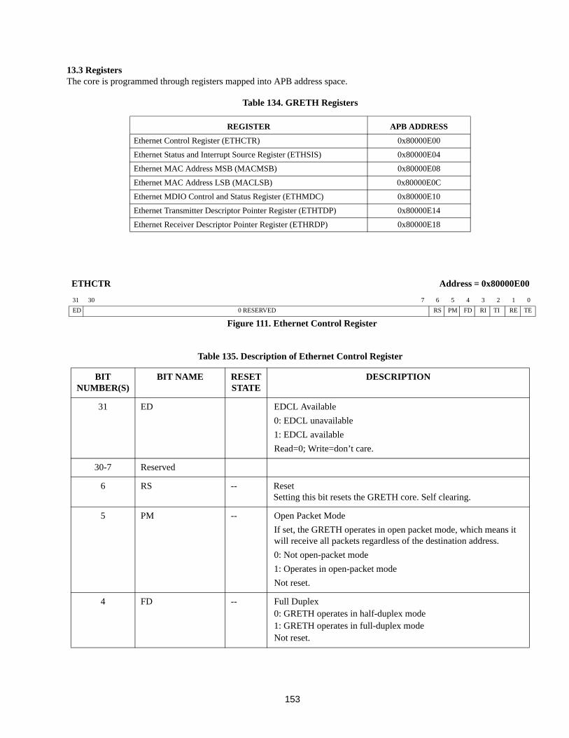
153
13.3 Registers The core is programmed through registers mapped into APB address space.
Table 134. GRETH Registers
REGISTER APB ADDRESS
Ethernet Control Register (ETHCTR) 0x80000E00
Ethernet Status and Interrupt Source Register (ETHSIS) 0x80000E04
Ethernet MAC Address MSB (MACMSB) 0x80000E08
Ethernet MAC Address LSB (MACLSB) 0x80000E0C
Ethernet MDIO Control and Status Register (ETHMDC) 0x80000E10
Ethernet Transmitter Descriptor Pointer Register (ETHTDP) 0x80000E14
Ethernet Receiver Descriptor Pointer Register (ETHRDP) 0x80000E18
Table 135. Description of Ethernet Control Register
BIT NUMBER(S)
BIT NAME RESET STATE
DESCRIPTION
31 ED EDCL Available
0: EDCL unavailable
1: EDCL available
Read=0; Write=don’t care.
30-7 Reserved
6 RS -- ResetSetting this bit resets the GRETH core. Self clearing.
5 PM -- Open Packet Mode
If set, the GRETH operates in open packet mode, which means it will receive all packets regardless of the destination address.
0: Not open-packet mode
1: Operates in open-packet mode
Not reset.
4 FD -- Full Duplex0: GRETH operates in half-duplex mode1: GRETH operates in full-duplex modeNot reset.
ETHCTR Address = 0x80000E00
31 30 7 6 5 4 3 2 1 0
ED 0 RESERVED RS PM FD RI TI RE TE
Figure 111. Ethernet Control Register
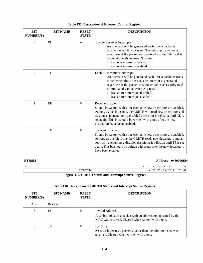
154
BIT NUMBER(S)
BIT NAME RESET STATE
DESCRIPTION
3 RI -- Enable Receiver InterruptsAn interrupt will be generated each time a packet is received when this bit is set. The interrupt is generated regardless if the packet was received successfully or if it terminated with an error. Not reset.0: Receiver interrupts disabled1: Receiver interrupts enabled
2 TI Enable Transmitter InterruptsAn interrupt will be generated each time a packet is trans-mitted when this bit is set. The interrupt is generated regardless if the packet was transmitted successfully or if it terminated with an error. Not reset.0: Transmitter interrupts disabled1: Transmitter interrupts enabled
1 RE 0 Receive EnableShould be written with a one each time new descriptors are enabled. As long as this bit is one, the GRETH will read new descriptors and as soon as it encounters a disabled descriptor it will stop until RE is set again. This bit should be written with a one after the new descriptors have been enabled.
0 TE 0 Transmit EnableShould be written with a one each time new descriptors are enabled. As long as this bit is one the GRETH reads new descriptors and as soon as it encounters a disabled descriptor it will stop until TE is set again. This bit should be written with a one after the new descriptors have been enabled.
Table 136. Description of GRETH Status and Interrupt Source Register
BIT NUMBER(S)
BIT NAME RESET STATE
DESCRIPTION
31-8 Reserved
7 IA 0 Invalid Address
A set bit indicates a packet with an address not accepted by the MAC was received. Cleared when written with a one.
6 TS 0 Too SmallA set bit indicates a packet smaller than the minimum size was received. Cleared when written with a one.
Table 135. Description of Ethernet Control Register
ETHSIS Address = 0x80000E04
31 8 7 6 5 4 3 2 1 0
RESERVED IA TS TA RA TI RI TE RE
Figure 112. GRETH Status and Interrupt Source Register
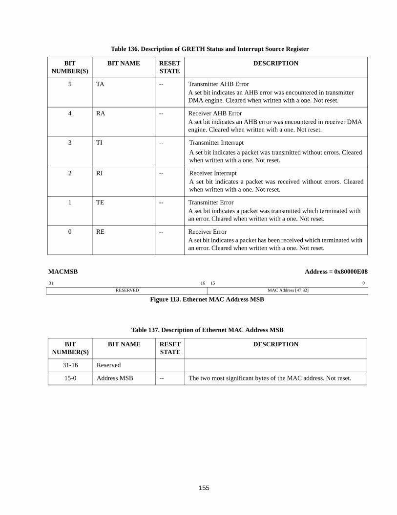
155
BIT NUMBER(S)
BIT NAME RESET STATE
DESCRIPTION
5 TA -- Transmitter AHB ErrorA set bit indicates an AHB error was encountered in transmitter DMA engine. Cleared when written with a one. Not reset.
4 RA -- Receiver AHB ErrorA set bit indicates an AHB error was encountered in receiver DMA engine. Cleared when written with a one. Not reset.
3 TI -- Transmitter Interrupt
A set bit indicates a packet was transmitted without errors. Cleared when written with a one. Not reset.
2 RI -- Receiver InterruptA set bit indicates a packet was received without errors. Clearedwhen written with a one. Not reset.
1 TE -- Transmitter ErrorA set bit indicates a packet was transmitted which terminated with an error. Cleared when written with a one. Not reset.
0 RE -- Receiver ErrorA set bit indicates a packet has been received which terminated with an error. Cleared when written with a one. Not reset.
Table 137. Description of Ethernet MAC Address MSB
BIT NUMBER(S)
BIT NAME RESET STATE
DESCRIPTION
31-16 Reserved
15-0 Address MSB -- The two most significant bytes of the MAC address. Not reset.
Table 136. Description of GRETH Status and Interrupt Source Register
MACMSB Address = 0x80000E08
31 16 15 0
RESERVED MAC Address [47:32]
Figure 113. Ethernet MAC Address MSB
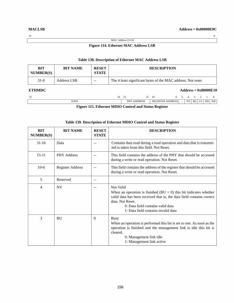
156
Table 138. Description of Ethernet MAC Address LSB
BIT NUMBER(S)
BIT NAME RESET STATE
DESCRIPTION
31-0 Address LSB -- The 4 least significant bytes of the MAC address. Not reset.
Table 139. Description of Ethernet MDIO Control and Status Register
BIT NUMBER(S)
BIT NAME RESET STATE
DESCRIPTION
31-16 Data -- Contains data read during a read operation and data that is transmit-ted is taken from this field. Not Reset.
15-11 PHY Address -- This field contains the address of the PHY that should be accessedduring a write or read operation. Not Reset.
10-6 Register Address -- This field contains the address of the register that should be accessedduring a write or read operation. Not Reset.
5 Reserved --
4 NV -- Not ValidWhen an operation is finished (BU = 0) this bit indicates whethervalid data has been received that is, the data field contains correctdata. Not Reset.
0: Data field contains valid data1: Data field contains invalid data
3 BU 0 BusyWhen an operation is performed this bit is set to one. As soon as theoperation is finished and the management link is idle this bit iscleared.
0: Management link idle1: Management link active
ETHMDC Address = 0x80000E10
31 16 15 11 10 6 5 4 3 2 1 0
DATA PHY ADDRESS REGISTER ADDRESS - NV BU LF RD WR
Figure 115. Ethernet MDIO Control and Status Register
MACLSB Address = 0x80000E0C
31 0
MAC Address [31:0]
Figure 114. Ethernet MAC Address LSB
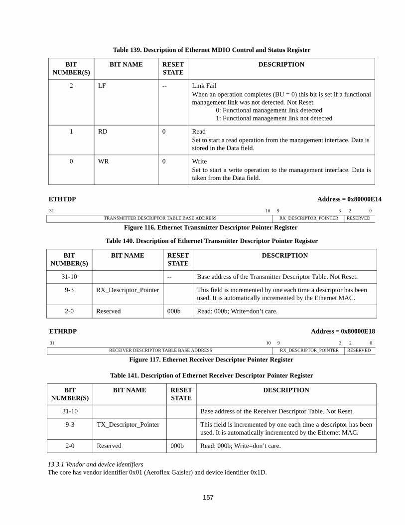
157
13.3.1 Vendor and device identifiersThe core has vendor identifier 0x01 (Aeroflex Gaisler) and device identifier 0x1D.
BIT NUMBER(S)
BIT NAME RESET STATE
DESCRIPTION
2 LF -- Link FailWhen an operation completes (BU = 0) this bit is set if a functionalmanagement link was not detected. Not Reset.
0: Functional management link detected1: Functional management link not detected
1 RD 0 ReadSet to start a read operation from the management interface. Data is stored in the Data field.
0 WR 0 WriteSet to start a write operation to the management interface. Data istaken from the Data field.
Table 140. Description of Ethernet Transmitter Descriptor Pointer Register
BIT NUMBER(S)
BIT NAME RESET STATE
DESCRIPTION
31-10 -- Base address of the Transmitter Descriptor Table. Not Reset.
9-3 RX_Descriptor_Pointer This field is incremented by one each time a descriptor has beenused. It is automatically incremented by the Ethernet MAC.
2-0 Reserved 000b Read: 000b; Write=don’t care.
Table 141. Description of Ethernet Receiver Descriptor Pointer Register
BIT NUMBER(S)
BIT NAME RESET STATE
DESCRIPTION
31-10 Base address of the Receiver Descriptor Table. Not Reset.
9-3 TX_Descriptor_Pointer This field is incremented by one each time a descriptor has beenused. It is automatically incremented by the Ethernet MAC.
2-0 Reserved 000b Read: 000b; Write=don’t care.
Table 139. Description of Ethernet MDIO Control and Status Register
ETHTDP Address = 0x80000E14
31 10 9 3 2 0
TRANSMITTER DESCRIPTOR TABLE BASE ADDRESS RX_DESCRIPTOR_POINTER RESERVED
Figure 116. Ethernet Transmitter Descriptor Pointer Register
ETHRDP Address = 0x80000E18
31 10 9 3 2 0
RECEIVER DESCRIPTOR TABLE BASE ADDRESS RX_DESCRIPTOR_POINTER RESERVED
Figure 117. Ethernet Receiver Descriptor Pointer Register
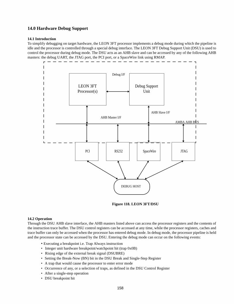
158
14.0 Hardware Debug Support
14.1 IntroductionTo simplify debugging on target hardware, the LEON 3FT processor implements a debug mode during which the pipeline is idle and the processor is controlled through a special debug interface. The LEON 3FT Debug Support Unit (DSU) is used to control the processor during debug mode. The DSU acts as an AHB slave and can be accessed by any of the following AHB masters: the debug UART, the JTAG port, the PCI port, or a SpaceWire link using RMAP.
14.2 OperationThrough the DSU AHB slave interface, the AHB masters listed above can access the processor registers and the contents of the instruction trace buffer. The DSU control registers can be accessed at any time, while the processor registers, caches and trace buffer can only be accessed when the processor has entered debug mode. In debug mode, the processor pipeline is held and the processor state can be accessed by the DSU. Entering the debug mode can occur on the following events:
• Executing a breakpoint i.e. Trap Always instruction• Integer unit hardware breakpoint/watchpoint hit (trap 0x0B)• Rising edge of the external break signal (DSUBRE)• Setting the Break-Now (BN) bit in the DSU Break and Single-Step Register• A trap that would cause the processor to enter error mode• Occurrence of any, or a selection of traps, as defined in the DSU Control Register• After a single-step operation• DSU breakpoint hit
Processor(s)LEON 3FT
Unit
AMBA AHB BUS
Debug Support
AHB Slave I/F
Debug I/F
AHB Master I/F
SpaceWire
DEBUG HOST
RS232 JTAGPCI
Figure 118. LEON 3FT/DSU
159
Debug mode can only be entered when the debug support unit is enabled by setting the DSUEN pin high. When debug mode is entered, the following actions are taken:
• PC and nPC are saved in temporary registers (accessible by the debug unit)• An output signal (DSUACT) is asserted to indicate the debug state• The timer unit is (optionally) stopped to freeze the LEON 3FT timers and watchdog
The instruction that caused the processor to enter debug mode is not executed and the processor state is kept unmodified. Execution is resumed by clearing the BN bit in the DSU Control Register or by de-asserting DSUEN. The timer unit will be re-enabled and execution will continue from the saved PC and nPC. Debug mode can also be entered after the processor has entered error mode, for instance when an application has terminated and halted the processor. Error mode can be reset and the processor restarted at any address.
When a processor is in debug mode, accesses to the ASI diagnostic area are forwarded to the IU, which performs accesses with the ASI equal to value in the DSU ASI Diagnostic Register and address consisting of 20 least-significant bits of the original address.
14.3 AHB Trace BufferThe AHB trace buffer consists of a circular buffer that stores AHB data transfers. The address, data, and various control sig-nals of the AHB bus are stored and can be read out for later analysis. The trace buffer is 128 bits wide and 128 lines deep. The information stored is indicated in the table below:
In addition to the AHB signals, the DSU time tag counter is also stored in the trace.
Table 142. AHB Trace Buffer Data Allocation
BITS NAME DEFINITION
127 AHB breakpoint hit Set to ‘1’ if a DSU AHB breakpoint hit occurred.
126 - Not used
125:96 Time tag DSU time tag counter
95 - Not used
94:80 Hirq AHB HIRQ[15:1]
79 Hwrite AHB HWRITE
78:77 Htrans AHB HTRANS
76:74 Hsize AHB HSIZE
73:71 Hburst AHB HBURST
70:67 Hmaster AHB HMASTER
66 Hmastlock AHB HMASTLOCK
65:64 Hresp AHB HRESP
63:32 Load/Store data AHB HRDATA or HWDATA
31:0 Load/Store address AHB HADDR
160
The trace buffer is enabled by setting the Enable (EN) bit in the AHB Trace Buffer Control Register. Each AHB transfer is then stored in the buffer in a circular manner. The address to which the next transfer is written is held in the Trace Buffer Index Register and is automatically incremented after each transfer. Tracing is stopped when the EN bit is cleared, or when an AHB breakpoint is hit. Tracing is temporarily suspended when the processor enters debug mode. Neither the trace buffer memory nor the breakpoint registers (see below) can be read/written by software when the trace buffer is enabled.
14.4 Instruction trace bufferThe instruction trace buffer consists of a circular buffer that stores executed instructions. The instruction trace buffer is located in the processor and read out via the DSU. The trace buffer is 128 bits wide and 128 lines deep. The information stored is indicated in the table below:
During tracing, one instruction is stored per line in the trace buffer with the exception of multi-cycle instructions. Multi-cycle instructions are entered two or three times in the trace buffer. For store instructions, bits 63:32 correspond to the store address on the first entry and to the stored data on the second entry (and the third in case of an STD instruction). Bit 126 is set on the second and third entry to indicate this. A double load (LDD) instruction is entered twice in the trace buffer with bits 63:32 containing the loaded data. Multiply and divide instructions are entered twice, but only the last entry contains the result. Bit 126 is set for the second entry. For FPU operation producing a double-precision result, the first entry puts the most-significant 32 bits of the results in bits 63:32, while the second entry puts the least-significant 32 bits in this field.
When the processor enters debug mode, tracing is suspended. The trace buffer and the AHB Trace Buffer Control Register can be read and written to, while the processor is in debug mode. During instruction tracing (processor in normal mode) the trace buffer and the AHB Trace Buffer Control Register can not be accessed
14.5 DSU memory mapThe DSU memory map can be seen in table 1.3 below. The base address is 0x90000000.
Table 143. Instruction Trace Buffer Data Allocation
BITS NAME DEFINITION
127 - Unused
126 Multi-cycle instruction Set to ‘1’ on the second and third instance of a multi-cycle instruction (LDD, ST or FPOP)
125:96 Time tag The value of the DSU time tag counter
95:64 Load/Store parameters Instruction result, Store address or Store data
63:34 Program counter Program counter (2 lsb bits removed since they are always zero)
33 Instruction trap Set to ‘1’ if traced instruction trapped
32 Processor error mode Set to ‘1’ if the traced instruction caused processor error mode
31:0 Opcode Instruction opcode
Table 144. DSU Memory Map
REGISTER ADDRESS
DSU Control Register 0x90000000
DSU Trace Buffer Time Tag Counter Register 0x90000008
DSU Break and Single-Step Register 0x90000020
161
AHB Trace Buffer Control Register 0x90000040
AHB Trace Buffer Index Register 0x90000044
AHB Trace Buffer Breakpoint Address Register 1 0x90000050
AHB Trace Buffer Breakpoint Mask Register 1 0x90000054
AHB Trace Buffer Breakpoint Address Register 2 0x90000058
AHB Trace Buffer Breakpoint Mask Register 2 0x9000005c
Instruction Trace Buffer 0x90100000 - 0x90110000
Instruction Trace Buffer Control Register 0x90110000
AHB Trace Buffer 0x90200000 - 0x90210000
IU Register File 0x90300000 - 0x90300FFC
FPU Register File 0x90301000 - 0x9030107C
IU Special Purpose Registers 0x90400000 - 0x904FFFFC
Y Register 0x90400000
PSR Register 0x90400004
WIM Register 0x90400008
TBR Register 0x9040000C
PC Register 0x90400010
NPC Register 0x90400014
FSR Register 0x90400018
CPSR Register 0x9040001C
DSU Trap Register 0x90400020
DSU ASI Diagnostic Access Register 0x90400024
ASR16 - ASR31 (when implemented) 0x90400040 - 0x9040007C
ASI Diagnostic Access (ASI = value in DSU ASI register, address = address[19:0])ASI = 0x9: Local instruction RAMASI = 0xB: Local data RAMASI = 0xC: Instruction cache tagsASI = 0xD: Instruction cache dataASI = 0xE: Data cache tagsASI = 0xF: Instruction cache data
0x90700000 - 0x907FFFFC
Table 144. DSU Memory Map
REGISTER ADDRESS
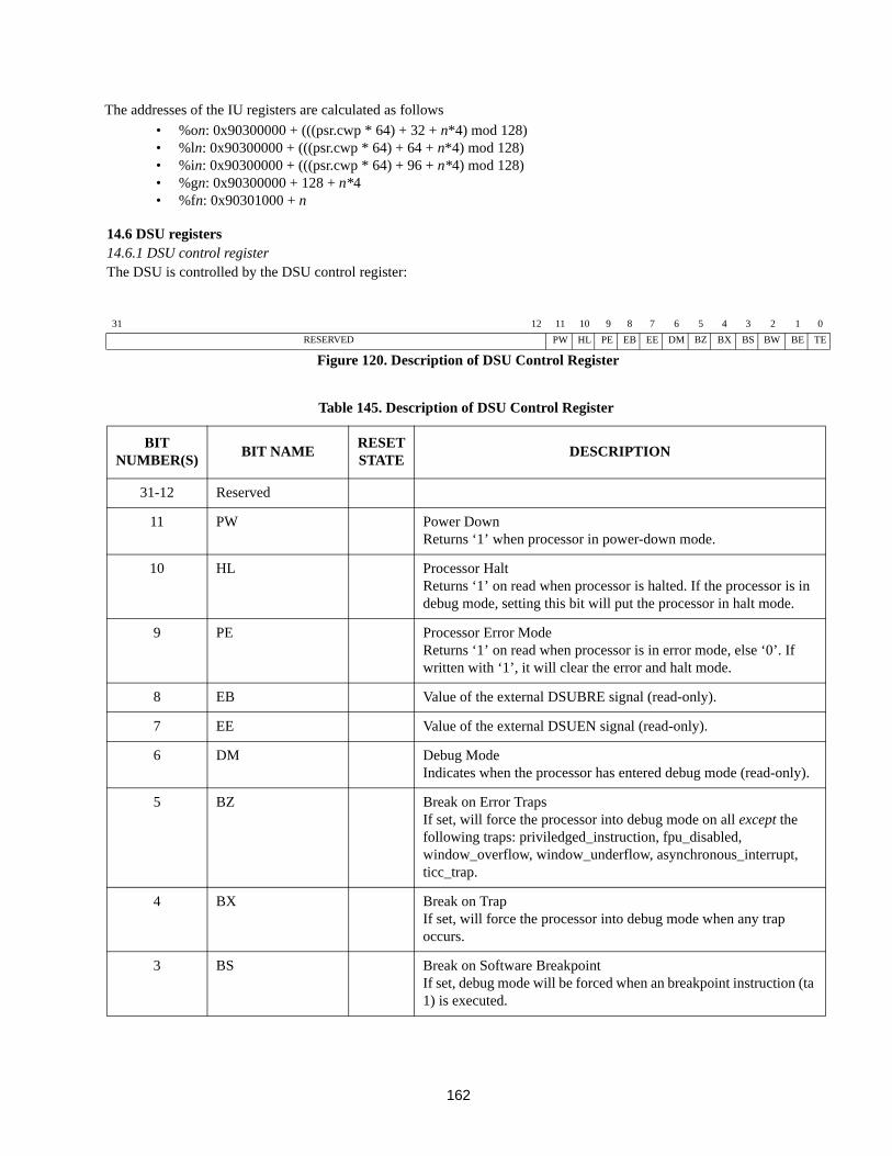
162
The addresses of the IU registers are calculated as follows
• %on: 0x90300000 + (((psr.cwp * 64) + 32 + n*4) mod 128)• %ln: 0x90300000 + (((psr.cwp * 64) + 64 + n*4) mod 128)• %in: 0x90300000 + (((psr.cwp * 64) + 96 + n*4) mod 128)• %gn: 0x90300000 + 128 + n*4• %fn: 0x90301000 + n
14.6 DSU registers14.6.1 DSU control registerThe DSU is controlled by the DSU control register:
Table 145. Description of DSU Control Register
BIT NUMBER(S)
BIT NAMERESET STATE
DESCRIPTION
31-12 Reserved
11 PW Power DownReturns ‘1’ when processor in power-down mode.
10 HL Processor HaltReturns ‘1’ on read when processor is halted. If the processor is in debug mode, setting this bit will put the processor in halt mode.
9 PE Processor Error ModeReturns ‘1’ on read when processor is in error mode, else ‘0’. If written with ‘1’, it will clear the error and halt mode.
8 EB Value of the external DSUBRE signal (read-only).
7 EE Value of the external DSUEN signal (read-only).
6 DM Debug ModeIndicates when the processor has entered debug mode (read-only).
5 BZ Break on Error TrapsIf set, will force the processor into debug mode on all except the following traps: priviledged_instruction, fpu_disabled, window_overflow, window_underflow, asynchronous_interrupt, ticc_trap.
4 BX Break on TrapIf set, will force the processor into debug mode when any trap occurs.
3 BS Break on Software BreakpointIf set, debug mode will be forced when an breakpoint instruction (ta 1) is executed.
31 12 11 10 9 8 7 6 5 4 3 2 1 0
RESERVED PW HL PE EB EE DM BZ BX BS BW BE TE
Figure 120. Description of DSU Control Register
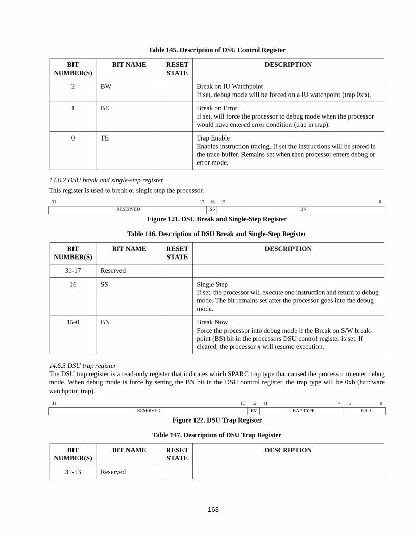
163
14.6.2 DSU break and single-step register
This register is used to break or single step the processor.
14.6.3 DSU trap registerThe DSU trap register is a read-only register that indicates which SPARC trap type that caused the processor to enter debugmode. When debug mode is force by setting the BN bit in the DSU control register, the trap type will be 0xb (hardwarewatchpoint trap).
BIT NUMBER(S)
BIT NAME RESET STATE
DESCRIPTION
2 BW Break on IU WatchpointIf set, debug mode will be forced on a IU watchpoint (trap 0xb).
1 BE Break on ErrorIf set, will force the processor to debug mode when the processor would have entered error condition (trap in trap).
0 TE Trap EnableEnables instruction tracing. If set the instructions will be stored in the trace buffer. Remains set when then processor enters debug or error mode.
31 17 16 15 0
RESERVED SS BN
Figure 121. DSU Break and Single-Step Register
Table 146. Description of DSU Break and Single-Step Register
BIT NUMBER(S)
BIT NAME RESET STATE
DESCRIPTION
31-17 Reserved
16 SS Single StepIf set, the processor will execute one instruction and return to debug mode. The bit remains set after the processor goes into the debug mode.
15-0 BN Break NowForce the processor into debug mode if the Break on S/W break-point (BS) bit in the processors DSU control register is set. If cleared, the processor x will resume execution.
31 13 12 11 4 3 0
RESERVED EM TRAP TYPE 0000
Figure 122. DSU Trap Register
Table 147. Description of DSU Trap Register
BIT NUMBER(S)
BIT NAME RESET STATE
DESCRIPTION
31-13 Reserved
Table 145. Description of DSU Control Register
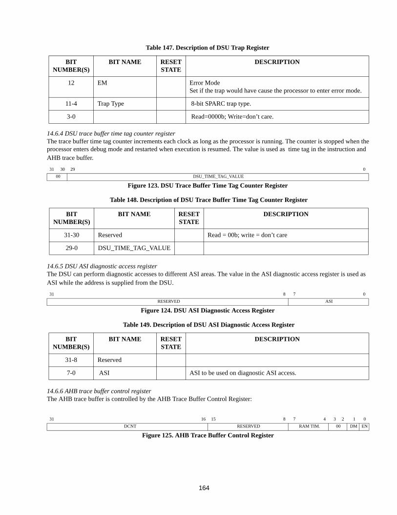
164
14.6.4 DSU trace buffer time tag counter registerThe trace buffer time tag counter increments each clock as long as the processor is running. The counter is stopped when the processor enters debug mode and restarted when execution is resumed. The value is used as time tag in the instruction and AHB trace buffer.
14.6.5 DSU ASI diagnostic access registerThe DSU can perform diagnostic accesses to different ASI areas. The value in the ASI diagnostic access register is used as ASI while the address is supplied from the DSU.
14.6.6 AHB trace buffer control registerThe AHB trace buffer is controlled by the AHB Trace Buffer Control Register:
BIT NUMBER(S)
BIT NAME RESET STATE
DESCRIPTION
12 EM Error ModeSet if the trap would have cause the processor to enter error mode.
11-4 Trap Type 8-bit SPARC trap type.
3-0 Read=0000b; Write=don’t care.
31 30 29 0
00 DSU_TIME_TAG_VALUE
Figure 123. DSU Trace Buffer Time Tag Counter Register
Table 148. Description of DSU Trace Buffer Time Tag Counter Register
BIT NUMBER(S)
BIT NAME RESET STATE
DESCRIPTION
31-30 Reserved Read = 00b; write = don’t care
29-0 DSU_TIME_TAG_VALUE
31 8 7 0
RESERVED ASI
Figure 124. DSU ASI Diagnostic Access Register
Table 149. Description of DSU ASI Diagnostic Access Register
BIT NUMBER(S)
BIT NAME RESET STATE
DESCRIPTION
31-8 Reserved
7-0 ASI ASI to be used on diagnostic ASI access.
31 16 15 8 7 4 3 2 1 0
DCNT RESERVED RAM TIM. 00 DM EN
Figure 125. AHB Trace Buffer Control Register
Table 147. Description of DSU Trap Register
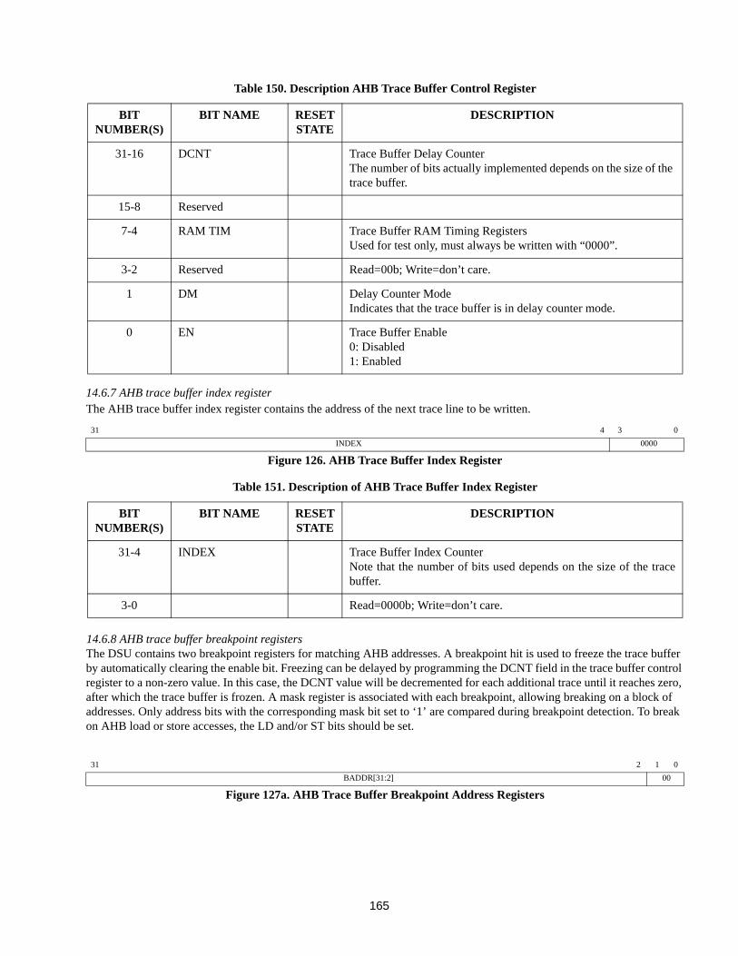
165
14.6.7 AHB trace buffer index registerThe AHB trace buffer index register contains the address of the next trace line to be written.
14.6.8 AHB trace buffer breakpoint registersThe DSU contains two breakpoint registers for matching AHB addresses. A breakpoint hit is used to freeze the trace buffer by automatically clearing the enable bit. Freezing can be delayed by programming the DCNT field in the trace buffer control register to a non-zero value. In this case, the DCNT value will be decremented for each additional trace until it reaches zero, after which the trace buffer is frozen. A mask register is associated with each breakpoint, allowing breaking on a block of addresses. Only address bits with the corresponding mask bit set to ‘1’ are compared during breakpoint detection. To break on AHB load or store accesses, the LD and/or ST bits should be set.
Table 150. Description AHB Trace Buffer Control Register
BIT NUMBER(S)
BIT NAME RESET STATE
DESCRIPTION
31-16 DCNT Trace Buffer Delay CounterThe number of bits actually implemented depends on the size of the trace buffer.
15-8 Reserved
7-4 RAM TIM Trace Buffer RAM Timing RegistersUsed for test only, must always be written with “0000”.
3-2 Reserved Read=00b; Write=don’t care.
1 DM Delay Counter ModeIndicates that the trace buffer is in delay counter mode.
0 EN Trace Buffer Enable0: Disabled1: Enabled
31 4 3 0
INDEX 0000
Figure 126. AHB Trace Buffer Index Register
Table 151. Description of AHB Trace Buffer Index Register
BIT NUMBER(S)
BIT NAME RESET STATE
DESCRIPTION
31-4 INDEX Trace Buffer Index CounterNote that the number of bits used depends on the size of the tracebuffer.
3-0 Read=0000b; Write=don’t care.
31 2 1 0
BADDR[31:2] 00
Figure 127a. AHB Trace Buffer Breakpoint Address Registers
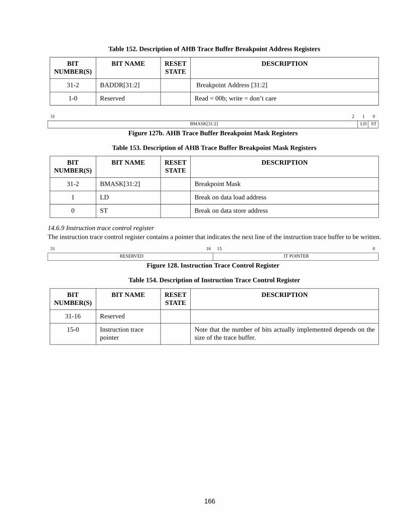
166
14.6.9 Instruction trace control registerThe instruction trace control register contains a pointer that indicates the next line of the instruction trace buffer to be written.
Table 152. Description of AHB Trace Buffer Breakpoint Address Registers
BIT NUMBER(S)
BIT NAME RESET STATE
DESCRIPTION
31-2 BADDR[31:2] Breakpoint Address [31:2]
1-0 Reserved Read = 00b; write = don’t care
31 2 1 0
BMASK[31:2] LD ST
Figure 127b. AHB Trace Buffer Breakpoint Mask Registers
Table 153. Description of AHB Trace Buffer Breakpoint Mask Registers
BIT NUMBER(S)
BIT NAME RESET STATE
DESCRIPTION
31-2 BMASK[31:2] Breakpoint Mask
1 LD Break on data load address
0 ST Break on data store address
31 16 15 0
RESERVED IT POINTER
Figure 128. Instruction Trace Control Register
Table 154. Description of Instruction Trace Control Register
BIT NUMBER(S)
BIT NAME RESET STATE
DESCRIPTION
31-16 Reserved
15-0 Instruction trace pointer
Note that the number of bits actually implemented depends on thesize of the trace buffer.
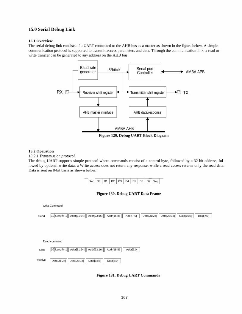
167
15.0 Serial Debug Link
15.1 OverviewThe serial debug link consists of a UART connected to the AHB bus as a master as shown in the figure below. A simple communication protocol is supported to transmit access parameters and data. Through the communication link, a read or write transfer can be generated to any address on the AHB bus.
15.2 Operation15.2.1 Transmission protocolThe debug UART supports simple protocol where commands consist of a control byte, followed by a 32-bit address, fol-lowed by optional write data. a Write access does not return any response, while a read access returns only the read data.Data is sent on 8-bit basis as shown below.
RX TXReceiver shift register Transmitter shift register
AHB master interface AHB data/response
AMBA AHB
Serial portController
8*bitclkBaud-rategenerator AMBA APB
Figure 129. Debug UART Block Diagram
Start D0 StopD6D5D4D3D2D1 D7
Figure 130. Debug UART Data Frame
Write Command
11 Length -1 Addr[31:24] Addr[7:0]Addr[15:8]Addr[23:16] Data[31:24] Data[7:0]Data[15:8]Data[23:16]Send
10 Length -1 Addr[31:24] Addr[7:0]Addr[15:8]Addr[23:16]Send
Read command
Receive Data[31:24] Data[7:0]Data[15:8]Data[23:16]
Figure 131. Debug UART Commands
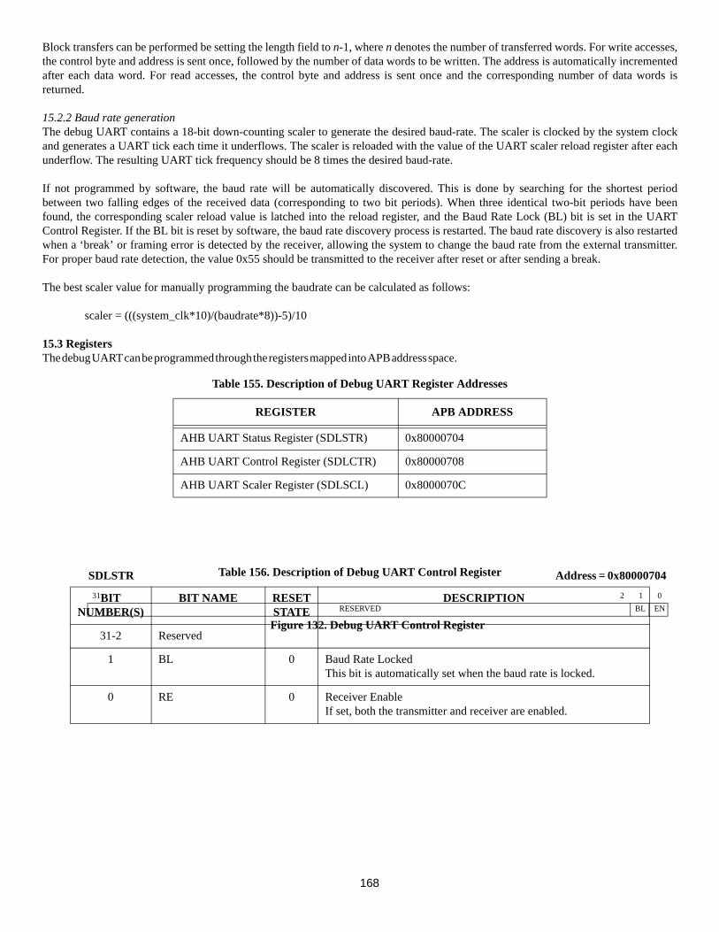
168
Block transfers can be performed be setting the length field to n-1, where n denotes the number of transferred words. For write accesses,the control byte and address is sent once, followed by the number of data words to be written. The address is automatically incrementedafter each data word. For read accesses, the control byte and address is sent once and the corresponding number of data words isreturned.
15.2.2 Baud rate generationThe debug UART contains a 18-bit down-counting scaler to generate the desired baud-rate. The scaler is clocked by the system clockand generates a UART tick each time it underflows. The scaler is reloaded with the value of the UART scaler reload register after eachunderflow. The resulting UART tick frequency should be 8 times the desired baud-rate.
If not programmed by software, the baud rate will be automatically discovered. This is done by searching for the shortest periodbetween two falling edges of the received data (corresponding to two bit periods). When three identical two-bit periods have beenfound, the corresponding scaler reload value is latched into the reload register, and the Baud Rate Lock (BL) bit is set in the UARTControl Register. If the BL bit is reset by software, the baud rate discovery process is restarted. The baud rate discovery is also restartedwhen a ‘break’ or framing error is detected by the receiver, allowing the system to change the baud rate from the external transmitter.For proper baud rate detection, the value 0x55 should be transmitted to the receiver after reset or after sending a break.
The best scaler value for manually programming the baudrate can be calculated as follows:
scaler = (((system_clk*10)/(baudrate*8))-5)/10
15.3 RegistersThe debug UART can be programmed through the registers mapped into APB address space.
Table 155. Description of Debug UART Register Addresses
REGISTER APB ADDRESS
AHB UART Status Register (SDLSTR) 0x80000704
AHB UART Control Register (SDLCTR) 0x80000708
AHB UART Scaler Register (SDLSCL) 0x8000070C
Table 156. Description of Debug UART Control Register
BIT NUMBER(S)
BIT NAME RESET STATE
DESCRIPTION
31-2 Reserved
1 BL 0 Baud Rate LockedThis bit is automatically set when the baud rate is locked.
0 RE 0 Receiver EnableIf set, both the transmitter and receiver are enabled.
SDLSTR Address = 0x80000704
31 2 1 0
RESERVED BL EN
Figure 132. Debug UART Control Register
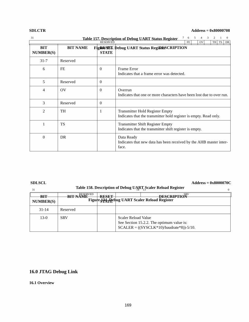
169
16.0 JTAG Debug Link
16.1 Overview
Table 157. Description of Debug UART Status Register
BIT NUMBER(S)
BIT NAME RESET STATE
DESCRIPTION
31-7 Reserved
6 FE 0 Frame ErrorIndicates that a frame error was detected.
5 Reserved 0
4 OV 0 OverrunIndicates that one or more characters have been lost due to over run.
3 Reserved 0
2 TH 1 Transmitter Hold Register EmptyIndicates that the transmitter hold register is empty. Read only.
1 TS Transmitter Shift Register EmptyIndicates that the transmitter shift register is empty.
0 DR Data ReadyIndicates that new data has been received by the AHB master inter-face.
Table 158. Description of Debug UART Scaler Reload Register
BIT NUMBER(S)
BIT NAME RESET STATE
DESCRIPTION
31-14 Reserved
13-0 SRV Scaler Reload ValueSee Section 15.2.2. The optimum value is:SCALER = ((SYSCLK*10)/baudrate*8))-5/10.
SDLCTR Address = 0x80000708
31 7 6 5 4 3 2 1 0
RESERVED FE OV TH TS DR
Figure 133. Debug UART Status Register
SDLSCL Address = 0x8000070C
31 14 13 0
RESERVED SRV
Figure 134. Debug UART Scaler Reload Register
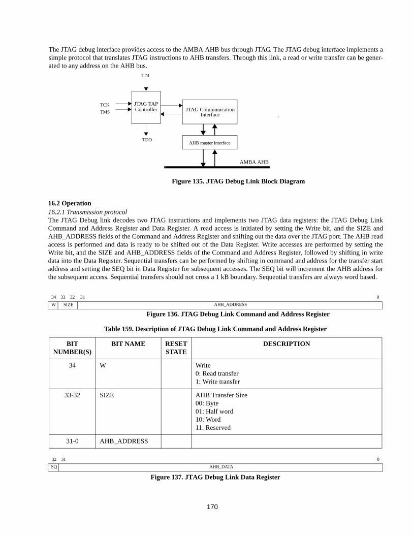
170
The JTAG debug interface provides access to the AMBA AHB bus through JTAG. The JTAG debug interface implements asimple protocol that translates JTAG instructions to AHB transfers. Through this link, a read or write transfer can be gener-ated to any address on the AHB bus.
16.2 Operation16.2.1 Transmission protocolThe JTAG Debug link decodes two JTAG instructions and implements two JTAG data registers: the JTAG Debug LinkCommand and Address Register and Data Register. A read access is initiated by setting the Write bit, and the SIZE andAHB_ADDRESS fields of the Command and Address Register and shifting out the data over the JTAG port. The AHB readaccess is performed and data is ready to be shifted out of the Data Register. Write accesses are performed by setting theWrite bit, and the SIZE and AHB_ADDRESS fields of the Command and Address Register, followed by shifting in writedata into the Data Register. Sequential transfers can be performed by shifting in command and address for the transfer startaddress and setting the SEQ bit in Data Register for subsequent accesses. The SEQ bit will increment the AHB address forthe subsequent access. Sequential transfers should not cross a 1 kB boundary. Sequential transfers are always word based.
34 33 32 31 0
W SIZE AHB_ADDRESS
Figure 136. JTAG Debug Link Command and Address Register
Table 159. Description of JTAG Debug Link Command and Address Register
BIT NUMBER(S)
BIT NAME RESET STATE
DESCRIPTION
34 W Write0: Read transfer1: Write transfer
33-32 SIZE AHB Transfer Size00: Byte01: Half word10: Word11: Reserved
31-0 AHB_ADDRESS
32 31 0
SQ AHB_DATA
Figure 137. JTAG Debug Link Data Register
Figure 135. JTAG Debug Link Block Diagram
AHB master interface
AMBA AHB
JTAG CommunicationInterface
JTAG TAPController
TCK
TMS
TDI
TDO
171
16.3 RegistersThe core does not implement any registers mapped in the AMBA AHB or APB address space.
16.4 Vendor and device identifiersThe core has vendor identifier 0x01 (Gaisler Research) and device identifier 0x01C.
17.0 CLKGATE Clock Gating Unit
17.1 OverviewThe CLKGATE clock gating unit provides a means to save power by disabling the clock to unutilized core blocks. The unit
Table 160. Description of JTAG Debug Link Data Register
BIT NUMBER(S)
BIT NAME RESET STATE
DESCRIPTION
32 SQ Sequential Transfer0: Non-sequential transfer1: When read data is shifted out or write data shifted in, the subse-quent transfer will be to next word address.
31-0 AHB_DATA For byte and half-word transfers, data is aligned according to big-endian order where data with address offset 0 data is placed in MSB bits.
172
can enable and disable up to 7 individual clock signals or reset the core state and registers to default.
17.2 OperationThe operation of the clock gating unit is controlled through three registers: the unlock, clock enable and core reset registers. The clock enable register defines if a clock is enabled or disabled. A ‘1’ in a bit location will enable the corresponding clock, while a ‘0’ will disable the clock. The core reset register resets each core to a default state. A reset will be generated as long as the corresponding bit is set to ‘1’. The bits in clock enable and core reset registers can only be written when the corre-sponding bit in the unlock register is 1. If the a bit in the unlock register is 0, the corresponding bits in the clock enable and core reset registers cannot be written.
To gate the clock for a core, the following procedure should be applied:
1. Disable the core through software to make sure it does not initialize any AHB accesses
2. Write a 1 to the corresponding bit in the unlock register
3. Write a 0 to the corresponding bit in the clock enable register
4. Write a 0 to the corresponding bit in the unlock register
To enable the clock for a core, the following procedure should be applied
1. Write a 1 to the corresponding bit in the unlock register
2. Write a 1 to the corresponding bit in the clock enable register
3. Write a 0 to the corresponding bit in the unlock register
Repeat this procedure to reset a specific core using the core reset register in place of the clock enable register.
The cores connected to the clock gating unit are defined in the table below:
Table 161. Clocks Controlled by CLKGATE Unit
17.3 RegistersTable 161 shows the clock gating unit registers. The base address for the registers is 0x80000600.
BIT FUNCTIONAL MODE
0 GRSPW Spacewire link 0
1 GRSPW Spacewire link 1
2 GRSPW Spacewire link 2
3 GRSPW Spacewire link 3
4 CAN core 1 & 2
5 GRETH 10/100 Mbit Ethernet MAC (AHB Clock)
6 GRPCI 32-bit PCI Bridge (AHB Clock)

173
Table 162. Clock Unit Control Registers
17.4 Vendor and device identifiersThe clock gating unit has vendor identifier 0x01 (Aeroflex Gaisler) and device identifier 0x02C.
APB ADDRESS FUNCTIONAL MODULERESET VALUE
0x80000600 Unlock Register 0000000
0x80000604 Clock Enable Register 1111111
0x80000608 Core Reset Register 0000000
174
COLORADO Toll Free: 800-645-8862 Fax: 719-594-8468
SE AND MID-ATLANTIC Tel: 321-951-4164 Fax: 321-951-4254
INTERNATIONALTel: 805-778-9229Fax: 805-778-1980
WEST COAST Tel: 949-362-2260Fax: 949-362-2266
NORTHEASTTel: 603-888-3975Fax: 603-888-4585
CENTRALTel: 719-594-8017Fax: 719-594-8468
w w w . a e r o f l e x . c o m i n f o - a m s @ a e r o f l e x . c o m
Our passion for performance is defined by threeattributes represented by these three icons:
solution-minded, performance-driven and customer-focused
Aeroflex Colorado Springs, Inc., reserves the right to make changes to any products and services herein at any time without notice. Consult Aeroflex or an authorized sales representative to verify that the information in this data sheet is current before using this product. Aeroflex does not assume any responsibility or liability arising out of the application or use of any product or service described herein, except as expressly agreed to in writing by Aeroflex; nor does the purchase, lease, or use of a product or service from Aeroflex convey a license under any patent rights, copyrights, trademark rights, or any other of the intellectual rights of Aeroflex or of third parties.
Aeroflex Colorado Springs, Inc.LEON Manual
Edits since March 11, 2010
Edits made March 11, 2010
Chapter 1.0, Section 1.2 Page 10Table 1 -Added ‘Version’ column with valuesAHBSTAT – Changed function statement to ‘AHB status register’Added underscore to CAN_OCAdded PCIARB line
Chapter 1.0, Section 1.6.2 Page 16Changed third sentence of paragraph to read, ‘See Section 17.0 for more details.’
Chapter 2, Section 2.2.9 Page 24Removed last sentence – ‘The external error signal will be asserted.’
Chapter 3, Section 3.16 Page 52Replaced Figure 20
Chapter 3, Section 3.16 Page 53Replaced Figure 21
Chapter 3, Section 3.16 Page 54Replaced Figure 22
Chapter 3, Section 3.16 Page 55Replaced Figure 23
Chapter 3, Section 3.16 Page 58Replaced Figure 26
Chapter 3, Section 3.16 Page 59Replaced Figure 27
Chapter 3, Section 3.16 Page 60Replaced Figure 28
Chapter 6, Section 6.4.4 Page 73Changed address on UARTSCR Scaler Register to 0x8000010C
A e r o f l e x C o l o r a d o S p r i n g s - D a t a s h e e t D e f i n i t i o n
A d v a n c e d D a t a s h e e t - P r o d u c t I n D e v e l o p m e n t
P r e l i m i n a r y D a t a s h e e t - S h i p p i n g P r o t o t y p e
D a t a s h e e t - S h i p p i n g Q M L & R e d u c e d H i - R e l
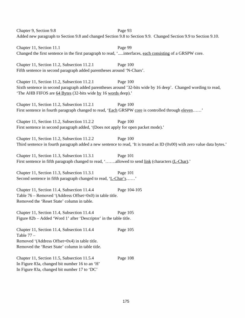
175
Chapter 9, Section 9.8 Page 93Added new paragraph to Section 9.8 and changed Section 9.8 to Section 9.9. Changed Section 9.9 to Section 9.10.
Chapter 11, Section 11.1 Page 99Changed the first sentence in the first paragraph to read, ‘.....interfaces, each consisting of a GRSPW core.
Chapter 11, Section 11.2, Subsection 11.2.1 Page 100Fifth sentence in second paragraph added parentheses around ‘N-Chars’.
Chapter 11, Section 11.2, Subsection 11.2.1 Page 100Sixth sentence in second paragraph added parentheses around ’32-bits wide by 16 deep’. Changed wording to read, ‘The AHB FIFOS are 64 Bytes (32-bits wide by 16 words deep).’
Chapter 11, Section 11.2, Subsection 11.2.1 Page 100First sentence in fourth paragraph changed to read, ‘Each GRSPW core is controlled through eleven……’
Chapter 11, Section 11.2, Subsection 11.2.2 Page 100First sentence in second paragraph added, ‘(Does not apply for open packet mode).’
Chapter 11, Section 11.2, Subsection 11.2.2 Page 100Third sentence in fourth paragraph added a new sentence to read, ‘It is treated as ID (0x00) with zero value data bytes.’
Chapter 11, Section 11.3, Subsection 11.3.1 Page 101First sentence in fifth paragraph changed to read, ‘…….allowed to send link (characters (L-Char).’
Chapter 11, Section 11.3, Subsection 11.3.1 Page 101Second sentence in fifth paragraph changed to read, ‘L-Char’s……’
Chapter 11, Section 11.4, Subsection 11.4.4 Page 104-105Table 76 – Removed ‘(Address Offset=0x0) in table title.Removed the ‘Reset State’ column in table.
Chapter 11, Section 11.4, Subsection 11.4.4 Page 105Figure 82b – Added ‘Word 1’ after ‘Descriptor’ in the table title.
Chapter 11, Section 11.4, Subsection 11.4.4 Page 105Table 77 – Removed ‘(Address Offset=0x4) in table title.Removed the ‘Reset State’ column in table title. Chapter 11, Section 11.5, Subsection 11.5.4 Page 108In Figure 83a, changed bit number 16 to an ‘H’ In Figure 83a, changed bit number 17 to ‘DC’
176
Chapter 11, Section 11.5, Subsection 11.5.4 Page 108-109Table 78 –Changed bit numbers in the first row to read, ’31-18’.Changed bit name in bit number 16 to ‘HC’.Added new description to bit number 16.Added bit number 17. Added description to bit number 17.Removed ‘Reset State’ column in table.
Chapter 11, Section 11.5, Subsection 11.5.4 Page 109Table 79 – Removed ‘Reset State’ column.
Chapter 11, Section 11.5, Subsection 11.5.4 Page 109 Table 80 –Removed ‘(Address Offset=0x8) in table title.Removed ‘Reset State’ column in table.
Chapter 11, Section 11.5, Subsection 11.5.4 Page 110 Table 81 –Removed ‘(Address Offset=0xC) in table title.Removed ‘Reset State’ column in table.
Chapter 11, Section 11.8 Page 118-119Table 85 –Added missing values to the ‘Reset State’ column for bit numbers 31, 30, 29, 28-18, 16, 15-12, 9, 8, 7, and 2.
Chapter 11, Section 11.8 Page 120Table 86 –Added missing values to the ‘Reset State’ column for bit numbers 31-24, 20-9, and 5.
Chapter 11, Section 11.8 Page 122Table 87 –Added missing values to the ‘Reset State’ column for bit numbers 31-8.
Chapter 11, Section 11.8 Page 122Table 88 –Added missing values to the ‘Reset State’ column for all bit numbers.
Chapter 11, Section 11.8 Page 122Table 89 –Added missing values to the ‘Reset State’ column for all bit numbers.
177
Chapter 11, Section 11.8 Page 122Table 90 –Corrected spelling for ‘Description’ in table title.Added missing values to the ‘Reset State’ column for bit number 31-8.Added description to bit number 5-0.
Chapter 11, Section 11.8 Page 122Table 91 –Added missing values to the ‘Reset State’ column for all bit numbers.
Chapter 11, Section 11.8 Page 124-125Table 92 –Added missing values to the ‘Reset State’ column for bit number 31-13, 12, 4, 3, and 2.
Chapter 11, Section 11.8 Page 126Table 93 –Added missing values to the ‘Reset State’ column for all bit numbers.
Chapter 11, Section 11.8 Page 126Table 94 –Added missing values to the ‘Reset State’ column for all bit numbers.
Chapter 11, Section 11.8 Page 126Table 95 –Added missing values to the ‘Reset State’ column for all bit numbers.
Chapter 13, Section 13.2, Subsection 13.2.16 Page 154Table 137 –Added bit name to bit number 15-0.
Chapter 15, Section 15.3 Page 167Changed sentence to read, ‘The STET….’Added spaces between all of the words in this sentence.Removed second sentence.
Chapter 15, Section 15.3 Page 167Table 155 – Changed table title to read, ‘Description of STET….’Removed extra spaces in title.
Chapter 15, Section 15.3 Page 167Figure 132 – Changed figure title to read, ‘DEBUG….’
178
Chapter 15, Section 15.3 Page 167Table 156 – Changed figure title to read, ‘Description of DEBUG….’
Edits made January 4, 2012
Chapter 1.0, Section 1.2 Page 10Added underscore to CAN_OC
Chapter 2.0, Section 2.1, Subsection 2.1.1 Page 17Changed second sentence of paragraph to read, ‘The integer unit has eight register windows providing a….’
Chapter 2.0, Section 2.2, Subsection 2.2.14 Page 26Changed first sentence of paragraph to read, ‘….implemented with a Bose-Chauduri-Hooquenghem….’
Chapter 2.0, Section 2.4, Subsection 2.4.5 Page 30Figure 8 - Changed figure title to read, ‘….Layout for 4kB per Way….’
Chapter 2.0, Section 3.5 Page 40-41Figure 12 – Changed labels in the ‘Memory Controller’ box: First label to read, ‘*ROMS[1:0]’; Fourth and fifth label to read, ‘*RAMS[4:0]’; Sixth label to read, ‘RWE[3:0]Added note to read, ‘*When the EDAC is enabled in 8-bit bus mode, only the first bank select (RAMS[0], ROMS[0] can be used.’
Figure 14 – Changed labels in the ‘Memory Controller’ box: First label to read, ‘ROMS[1:0]’; Fourth and fifth label to read, ‘RAMS[4:0]’
Chapter 3.0, Section 3.10 Page 43Changed fifth sentence of third paragraph to read, ‘….data memory while the top 20% is used….’
Chapter 3.0, Section 3.16 Page 56-57Figure 24 – Changed figure title to read, ‘….Write Cycle on a 32-bit bus’
Figure 25 - Changed figure title to read, ‘….SRAM 16-bit write cycle on a 16-bit bus’Added note to read, ‘*For 8-bit bus architectures, ADDR[27:0] and Data [31:24] and RWE[3] are used.’
179
Chapter 3.0, Section 3.16 Page 61Figure 29 – Changed label on next to the last bar to read, ‘*ADDR[27:2]’Changed label on the last bar to read, ‘*DATA[31:0]’Added note to read, ‘*For 16-bit I/O bus configurations ADDR[27:1] and Data [31:16] are used. For 8-bit I/O bus configurations ADDR[27:0] and Data[31:13] are used.’
Chapter 11.0, Section 11.5, Subsection 11.5.4 Page 108Table 78 –Description for Bit Number 17 added, ‘Data CRC’Changed second paragraph to read, ‘Append CRC….’Changed Bit Name for Bit Number 16 to read, ‘HC’
Chapter 11.0, Section 11.8 Page 119Table 85 –Added an ‘X’ to Reset State for Bit Number 7.
Chapter 13.0, Section 13.3 Page 155Table 138 –Changed Bit Name to read, ‘Address LSB’.
Chapter 15.0, Section 15.3 Page 168Table 157 – Changed Description for Bit Number 2, third sentence, to read, ‘Read only.’
Edits made January, 2012
Chapter 2.0, Section 2.4, Subsection 2.4.11 Page 34Fourth sentence, added space between ‘register’ and ‘%gl’.Fifth sentence, added space between ‘of’ and ‘%gl’.
Chapter 3.0, Section 3.5 Page 40Figure 12 –Changed note to read, ‘….(RAMS[0], ROMS[0])….’
Chapter 3.0, Section 3.9, Subsection 3.9.3 Page 42Added line space between Subsection 3.9.3 and Subsection 3.9.4
Chapter 3.0, Section 3.9, Subsection 3.9.6 Page 43Changed second sentence to read, ‘….internal system clock….’
Chapter 3.0, Section 3.10 Page 43Changed third paragraph, third sentence, removed comma after address.
180
Chapter 3.0, Section 3.16 Page 61Changed first sentence of note to read, ‘….ADDR[27:1]…’. Changed second sentence of note to read, ‘….ADDR[27:0]….’.
Chapter 11.0, Section 11.5, Subsection 11.5.4 Page 108Table 78 – Changed Description for Bit Number 16 to read, ‘Header CRC’.Changed third sentence of Description for Bit Number 16 - Added an ‘l’ to ‘length’.
Chapter 11.0, Section 11.5, Subsection 11.5.4 Page 110Table 81 –Removed ‘(Address Offset=0xC) in table title.
Chapter 11.0, Section 11.8 Page 124Table 92 -Added a ‘0’ to the Reset State column for Bit Number 16.Changed bit number to 15-13 rather than 13-15.
Chapter 13.0, Section 13.3 Page 155Table 138 – Changed Bit Name to Address LSB rather than Address CSB.
Chapter 15.0, Section 15.3 Page 167Table 156 –Added ‘0’ to Reset State Column for Bit Number(s) 1 and 0.
Chapter 15.0, Section 15.3 Page 168Table 157 - Corrected spelling of the word ‘characters’ under the Description for Bit Number 4.Under the Description of Bit Number 2, second paragraph, changed ‘Indicated’ to ‘Indicates’.
Edits made February 16, 2012
Chapter 2.0, Section 2.4, Subsection 2.4.11 Page 34Third sentence, added an ‘r’ to register.
Edits made March 1, 2012
Chapter 11.0, Section 11.8 Page 126Table 95 –Changed Bit Number to 9-3 from 9-4.Changed Bit Number 2-0 from 3-0.Changed Description under Bit Number 9-3, third sentence to read, ‘….increments to 128….’
181
Edits made March 12, 2012
Chapter 3.0, Section 3.14, Subsection 3.14.1 Page 49Changed Bit Name for Bit Number 9 to ‘RE’ from ‘SE’.Changed Description for Bit Number 9, first sentence to read, ‘….SRAM/SDRAM areas’.
Edits made March 20, 2012
Application Notes Page 174Added total of eight notes to this section.
Edits made April 2, 2012
Chapter 3.0, Section 3.10 Page 43Added paragraph four to read, ‘NOTE: When the EDAC is enabled in 8-bit bus mode, only the first bank select (ROMS[0], RAMS[0]) can be used.’
Chapter 3.0, Section 3.10 and Section 3.11 Page 43Removed a line space between Section 3.10 and Section 3.11.
Edits made May 22, 2012
Chapter 3.0, Section 3.2 Page 39PROM access clarification to paragraph 1.
Edits made June 20, 2012
Chapter 3.0, Section 3.2 Page 39PROM access clarification to paragraph 1.
Edits made July 23, 2012
Chapter 2.0, Section 2.4.6Page 30Changed paragraph wording to:Both instruction and data caches are flushed by executing the FLUSH instr uction or by writing to any location withASI=0x10 or ASI=0x11. In addition, the entire instruction cache is flushed by setting the FI bit in the cache control reg-ister (CCR). The entire data cache is flushed by seting the FD bit in the CCR. Cache flushing takes one cycle per cacheline, during which, the IU will not be halted and the caches are disabled. When the flush operation is completed, thecache resumes the state (disabled, enabled or frozen) indicated in the cache control register. Diagnostic access to thecache is not possible during a FLUSH operation and will cause a data exception (tt=0x09) if attempted.
Chapter 2.0, Section 2.5.1Page 35Edited table
182
Chapter 9.0, Section 9.6.1Page 96Changed paragraph text to:Both instruction and data caches are flushed by executing the FLUSH instr uction or by writing to any location withASI=0x10 or ASI=0x11. In addition, the entire instruction cache is flushed by setting the FI bit in the cache control reg-ister (CCR). The entire data cache is flushed by seting the FD bit in the CCR. Cache flushing takes one cycle per cacheline, during which, the IU will not be halted and the caches are disabled. When the flush operation is completed, thecache resumes the state (disabled, enabled or frozen) indicated in the cache control register. Diagnostic access to thecache is not possible during a FLUSH operation and will cause a data exception (tt=0x09) if attempted.
Chapter 9.0, Table 66 editedPage 96
Chapter 9, table 69 editedPage 97
183
APPLICATION NOTES
UT699 L1 Data and Instruction Cache (7/11)
UT699 Minimum System Design (6/11)
LEON 3FT Memory Configuration (6/11)
LEON 3FT Memory Configuration Worksheet (6/11)
GRMON Scripts for the LEON 3FT (6/11)
LEON 3FT to SuMMIT Interface (5/11)
UT699 External Memory Mapping (3/11)
UT699 Power Calculator (5/10)
LEON 3FT Sample SPARC Functions (4/12)

184

185