Embed Size (px)
Citation preview
41713HK/82912HKPC 018-11-0093 No.A2109-1/12
http://onsemi.com
Semiconductor Components Industries, LLC, 2013 April, 2013
STK433-890N-E
Overview The STK433-890N-E is 4 channels class-AB audio frequency power amplifier hybrid IC.
Application Audio Power amplifiers
Features Pin-to-pin compatible outputs ranging from 40W to 80W. Miniature package. Output load impedance: RL = 6 recommended. Allowable load shorted time: 0.3 second Allows the use of predesigned applications for standby and mute circuit.
Series model STK433-040N-E STK433-060N-E STK433-130N-E
Output1 (10%/1kHz) 40W 2ch 50W 2ch 150W 2ch
Output2 (0.4%/20Hz to 20kHz) 25W 2ch 35W 2ch 100W 2ch
Max. rating VCC (quiescent) 38V 46V 71.5V
Max. rating VCC (6) 36V 40V 63V
Recommended operating VCC (6) 24V 27V 44V
Dimensions (excluding pin height) 47.0mm25.6mm9.0mm 67.0mm25.6mm9.0mm
STK433-330N-E STK433-840N-E STK433-890N-E
Output1 (10%/1kHz) 150W 3ch 40W 4ch 80W 4ch
Output2 (0.4%/20Hz to 20kHz) 100W 3ch 25W 4ch 50W 4ch
Max. rating VCC (quiescent) 71.5V 38V 54V
Max. rating VCC (6) 63V 36V 47V
Recommended operating VCC (6) 44V 25V 34V
Dimensions (excluding pin height) 64.0mm36.6mm9.0mm 64.0mm31.1mm9.0mm 78.0mm44.1mm9.0mm
Specifications Absolute Maximum Ratings at Ta = 25C, Tc = 25C unless otherwise specified
Parameter Symbol Conditions Ratings Unit
Maximum power supply voltage VCC max (0) Non signal 54 V
VCC max (1) Signal, RL 6 47 V
VCC max (2) Signal, RL = 4 40 V
Minimum operation supply voltage VCC min 10 V
#13 Operating voltage *5 VST OFF max #13pin voltage -0.3 to +5.5 V
Thermal resistance j-c Per power transistor 2.1 C/W
Junction temperature Tj max Both the Tj max and Tc max
conditions must be met.
150 C
Operating substrate temperature Tc max 125 C
Storage temperature Tstg -30 to +125 C
Allowable time for load short-circuit
*4
ts VCC = 34V, RL = 6, f = 50Hz
PO = 50W, 1ch drive 0.3 s
Ordering number : ENA2109 Ordering number : ENA2101A Ordering number : ENA2109A
Thick-Film Hybrid IC
4ch class-AB Audio Power IC 80W4ch
Stresses exceeding Maximum Ratings may damage the device. Maximum Ratings are stress ratings only. Functional operation above the Recommended OperatingConditions is not implied. Extended exposure to stresses above the Recommended Operating Conditions may affect device reliability.
ORDERING INFORMATION See detailed ordering and shipping information on page 12 of this data sheet.
STK433-890N-E
No.A2109-2/12
Operating Characteristics at Tc = 25C, RL = 6 (Non-inductive Load), Rg = 600, VG = 30dB
Parameter Symbol
Conditions *2 Ratings
Unit VCC
[V]
f
[Hz]
PO
[W]
THD
[%] min typ max
Output power *1 PO 1 ±34 20 to 20k 0.6 47 50 W
PO 2 ±34 1k 10 80
Total harmonic distortion *1 THD 1 ±34 20 to 20k 5.0
VG=30dB
0.6%
THD 2 ±34 1k 0.02
Frequency characteristics *1 fL, fH ±34 1.0 +0 -3dB 20 to 50k Hz
Input impedance ri ±34 1k 1.0 55 k
Output noise voltage *3 VNO ±40 Rg=2.2k 1.0 mVrms
Quiescent current ICCO ±40 No load 90 150 210 mA
Quiescent current at stand-by ICST ±40 VST=0V 1.0 mA
Neutral voltage VN ±40 -70 0 +70 mV
#13 Stand-by ON threshold *5 VST ON ±34 Stand-by 0 0.6 V
#13 Stand-by OFF threshold *5 VST OFF ±34 Operation 2.5 3.0 5.5 V
Note *1. 1channel operation. *2. All tests are measured using a constant-voltage supply unless otherwise specified *3. The output noise voltage is peak value of an average-reading meter with a rms value scale (VTVM).
A regulated AC supply (50Hz) should be used to eliminate the effects of AC primary line flicker noise *4. Allowable time for load short-circuit and output noise voltage are measured using the specified transformer power
supply. *5. The impression voltage of ‘#13 (Stand-By) pin’ must not exceed the maximum rating.
Power amplifier operate by impressing voltage +2.5 to +5.5V to ‘#13 (Stand-By) pin’. * Please connect - PreVCC pin (#1 pin) with the stable minimum voltage.
and connect so that current does not flow in by reverse bias. * In case of heat sink design, we request customer to design in the condition to have assumed market. * The case of this Hybrid-IC is using thermosetting silicon adhesive (TSE322SX). * Weight of HIC : (typ) 37.0g
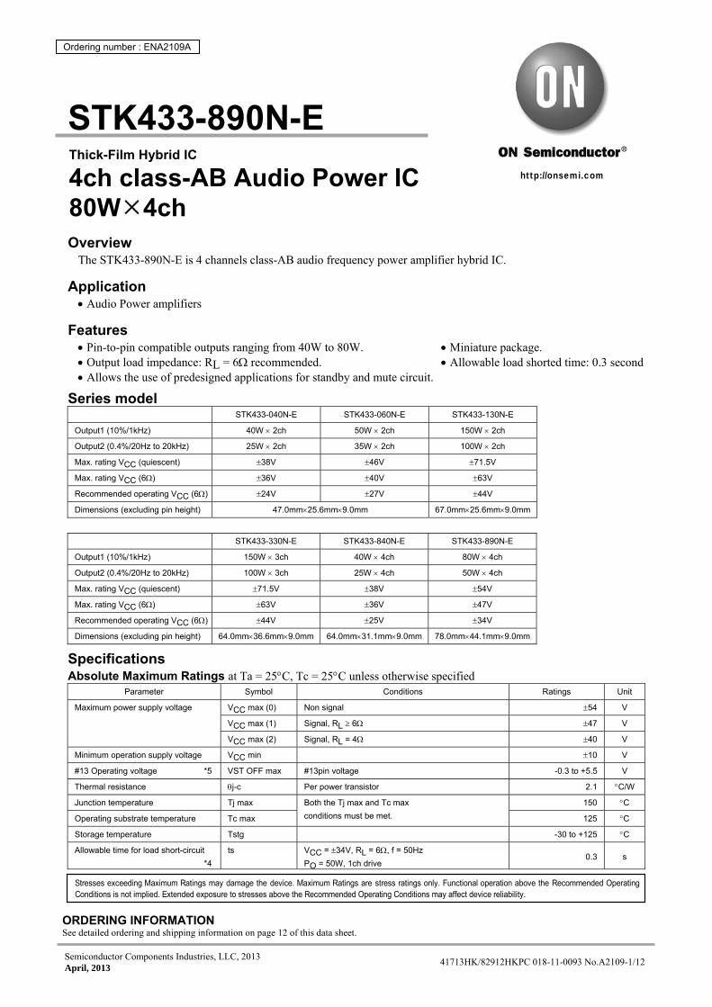
Outer carton dimensions (W×L×H) : 452mm×325mm×192mm Specified transformer power supply (Equivalent to MG-200)
+
+
10000F
10000F
500
500
DBA40C+VCC
-VCC
STK433-890N-E
No.A2109-3/12
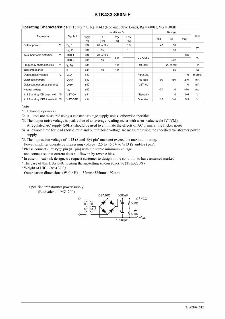
Package Dimensions unit : mm (typ)
RoHS directive pass Equivalent Circuit
9SUB
IC1+-
+-
Stand-byCircuit
Stand-byCircuit
38
202167 1918171614 1310151112 232254
IC2+-
+-
21
9.0
2.9
5.5
0.4
4.0
26.5
78.0
70.0
1 23
44.1
21.7
(R1.8)
5.0
3.6
22 2.0=44.0
2.0
(13.0)
0.5
STK433-890N-E
No.A2109-4/12
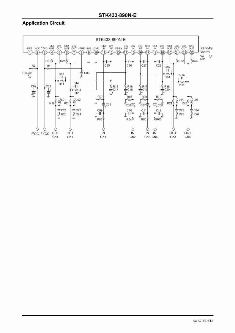
Application Circuit
12 13 14 151110987654321Stand-byControl
-VCC
-PRE -VCC +VCCCh1OUT
Ch1OUT
Ch2OUT
Ch2OUT +PRE
STK433-890N-E
R2
R27
R1
R28
R11
C13C04
R15C17
C26C25
SUB GNDCh1IN
Ch1NF ST-BY
Ch2NF
Ch2IN
C27
C11
R12
C14
1716
Ch3NF
Ch3IN
+
+R09
C07 +
+VCC
C28
21201918
Ch4IN
Ch4NF
Ch3OUT
Ch3OUT
Ch4OUT
Ch4OUT
2322
C02
+
C01+
C21
L01
R23
R19
OUTCh1
C22
L02
R24
R20
OUTCh1
INCh3
R13
C15
R14
R31
C16
C23
L04
R25
R21
OUTCh3
R29 R30
C24
L03
R26
R22
OUTCh4
C03+
R17C19
+
R18C20
+
R16C18
+
C10
R08
C06 +
INCh2
C09
R07
R03 R04 R05 R06
C05+
INCh1
C12
R10
C08+
INCh4
STK433-890N-E
No.A2109-6/12
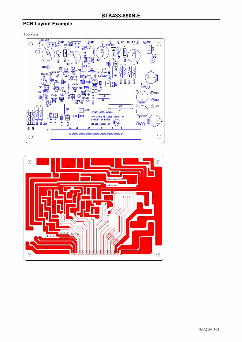
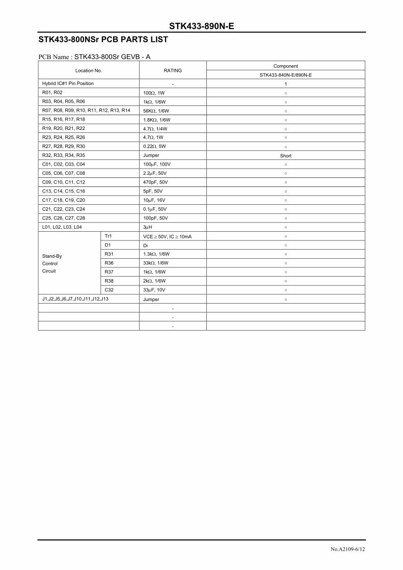
STK433-800NSr PCB PARTS LIST PCB Name : STK433-800Sr GEVB - A
Location No. RATING Component
STK433-840N-E/890N-E
Hybrid IC#1 Pin Position - 1
R01, R02 100, 1W
R03, R04, R05, R06 1k, 1/6W
R07, R08, R09, R10, R11, R12, R13, R14 56K, 1/6W
R15, R16, R17, R18 1.8K, 1/6W
R19, R20, R21, R22 4.7, 1/4W
R23, R24, R25, R26 4.7, 1W
R27, R28, R29, R30 0.22, 5W
R32, R33, R34, R35 Jumper Short
C01, C02, C03, C04 100F, 100V
C05, C06, C07, C08 2.2F, 50V
C09, C10, C11, C12 470pF, 50V
C13, C14, C15, C16 5pF, 50V
C17, C18, C19, C20 10F, 16V
C21, C22, C23, C24 0.1F, 50V
C25, C26, C27, C28 100pF, 50V
L01, L02, L03, L04 3H
Stand-By
Control
Circuit
Tr1 VCE 50V, IC 10mA
D1 Di
R31 1.3k, 1/6W
R36 33k, 1/6W
R37 1k, 1/6W
R38 2k, 1/6W
C32 33F, 10V
J1,J2,J5,J6,J7,J10,J11,J12,J13 Jumper
-
-
-
STK433-890N-E
No.A2109-7/12
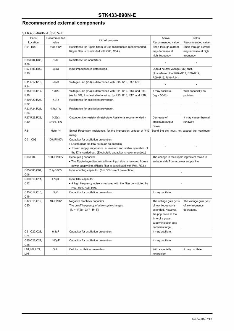
Recommended external components STK433-840N-E/890N-E
Parts
Location
Recommended
value Circuit purpose
Above
Recommended value
Below
Recommended value
R01, R02 100/1W Resistance for Ripple filters. (Fuse resistance is recommended.
Ripple filter is constituted with C03, C04.)
Short-through current
may decrease at
high frequency.
Short-through current
may increase at high
frequency.
R03,R04,R05,
R06
1k Resistance for input filters. - -
R07,R08,R09,
R10
56k Input impedance is determined. Output neutral voltage (VN) shift.
(It is referred that R07=R11, R08=R12,
R09=R13, R10=R14)
R11,R12,R13,
R14
56k Voltage Gain (VG) is determined with R15, R16, R17, R18 - -
R15,R16,R17,
R18
1.8k Voltage Gain (VG) is determined with R11, R12, R13, and R14.
(As for VG, it is desirable to set up by R15, R16, R17, and R18.)
It may oscillate.
(Vg < 30dB)
With especially no
problem
R19,R20,R21,
R22
4.7 Resistance for oscillation prevention. - -
R23,R24,R25,
R26
4.7/1W Resistance for oscillation prevention. - -
R27,R28,R29,
R30
0.22
10%, 5W
Output emitter resistor (Metal-plate Resistor is recommended.) Decrease of
Maximum output
Power
It may cause thermal
runaway
R31 Note *4 Select Restriction resistance, for the impression voltage of ‘#13 (Stand-By) pin’ must not exceed the maximum
rating.
C01, C02 100F/100V Capacitor for oscillation prevention.
Locate near the HIC as much as possible.
Power supply impedance is lowered and stable operation of
the IC is carried out. (Electrolytic capacitor is recommended.)
- -
C03,C04 100F/100V Decoupling capacitor
The Ripple ingredient mixed in an input side Is removed from a
power supply line. (Ripple filter is constituted with R01, R02.)
The change in the Ripple ingredient mixed in
an input side from a power supply line
C05,C06,C07,
C08
2.2F/50V Input coupling capacitor. (For DC current prevention.) -
C09,C10,C11,
C12
470pF Input filter capacitor
A high frequency noise is reduced with the filter constituted by
R03, R04, R05, R06.
-
C13,C14,C15,
C16
5pF Capacitor for oscillation prevention. It may oscillate.
C17,C18,C19,
C20
10F/10V Negative feedback capacitor.
The cutoff frequency of a low cycle changes.
(fL = 1/(2 C17 R15))
The voltage gain (VG)
of low frequency is
extended. However,
the pop noise at the
time of a power
supply injection also
becomes large.
The voltage gain (VG)
of low frequency
decreases.
C21,C22,C23,
C24
0.1F Capacitor for oscillation prevention. It may oscillate.
C25,C26,C27,
C28
100pF Capacitor for oscillation prevention. It may oscillate.
L01,L02,L03,
L04
3H Coil for oscillation prevention. With especially
no problem
It may oscillate.
STK433-890N-E
No.A2109-8/12
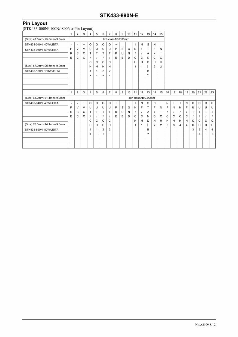
Pin Layout [STK433-000N/-100N/-800Nsr Pin Layout]
1 2 3 4 5 6 7 8 9 10 11 12 13 14 15
(Size) 47.0mm25.6mm9.0mm 2ch classAB/2.00mm
STK433-040N 40W/JEITA -
P
R
E
-
V
C
C
+
V
C
C
O
U
T
/
C
H
1
+
O
U
T
/
C
H
1
-
O
U
T
/
C
H
2
+
O
U
T
/
C
H
2
-
+
P
R
E
S
U
B
G
N
D
I
N
/
C
H
1
N
F
/
C
H
1
S
T
A
N
D
B
Y
N
F
/
C
H
2
I
N
/
C
H
2
STK433-060N 50W/JEITA
(Size) 67.0mm25.6mm9.0mm
STK433-130N 150W/JEITA
1 2 3 4 5 6 7 8 9 10 11 12 13 14 15 16 17 18 19 20 21 22 23
(Size) 64.0mm31.1mm9.0mm 4ch classAB/2.00mm
STK433-840N 40W/JEITA -
P
R
E
-
V
C
C
+
V
C
C
O
U
T
/
C
H
1
+
O
U
T
/
C
H
1
-
O
U
T
/
C
H
2
+
O
U
T
/
C
H
2
-
+
P
R
E
S
U
B
G
N
D
I
N
/
C
H
1
N
F
/
C
H
1
S
T
A
N
D
B
Y
N
F
/
C
H
2
I
N
/
C
H
2
N
F
/
C
H
3
I
N
/
C
H
3
I
N
/
C
H
4
N
F
/
C
H
4
O
U
T
/
C
H
3
-
O
U
T
/
C
H
3
+
O
U
T
/
C
H
4
-
O
U
T
/
C
H
4
+
(Size) 78.0mm44.1mm9.0mm
STK433-890N 80W/JEITA
STK433-890N-E
No.A2109-9/12
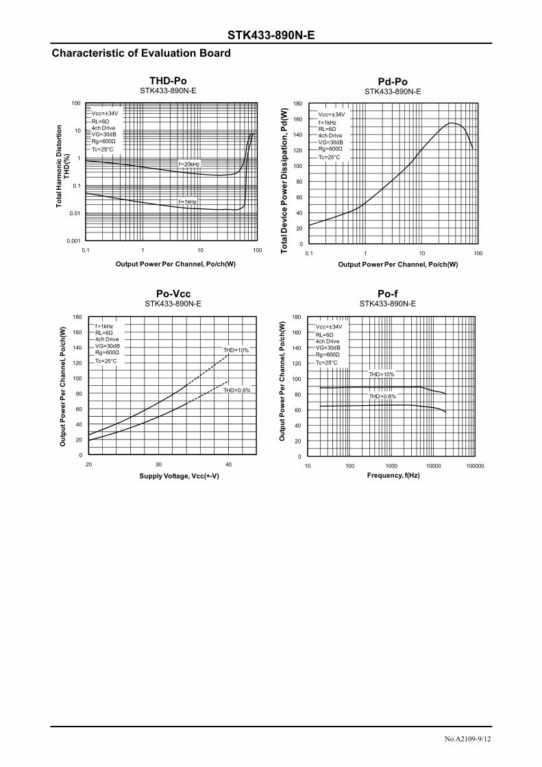
Characteristic of Evaluation Board
0.001
0.01
0.1
1
10
100
0.1 1 10 100
To
tal H
arm
on
ic D
isto
rtio
nT
HD
(%)
Output Power Per Channel, Po/ch(W)
THD-PoSTK433-890N-E
Vcc=±34V
RL=6Ω4ch DriveVG=30dBRg=600Ω
Tc=25°C
f=1kHz
f=20kHz
0
20
40
60
80
100
120
140
160
180
0.1 1 10 100To
tal D
evi
ce
Po
we
r Dis
sip
ati
on
, Pd
(W)
Output Power Per Channel, Po/ch(W)
Pd-PoSTK433-890N-E
Vcc=±34V
f=1kHzRL=6Ω4ch DriveVG=30dBRg=600Ω
Tc=25°C
0
20
40
60
80
100
120
140
160
180
20 30 40
Ou
tpu
t P
ow
er
Pe
r C
ha
nn
el,
Po
/ch
(W)
Supply Voltage, Vcc(+-V)
Po-VccSTK433-890N-E
f=1kHzRL=6Ω4ch DriveVG=30dBRg=600Ω
Tc=25°C
THD=0.6%
THD=10%
0
20
40
60
80
100
120
140
160
180
10 100 1000 10000 100000
Ou
tpu
t P
ow
er
Pe
r C
ha
nn
el,
Po
/ch
(W)
Frequency, f(Hz)
Po-fSTK433-890N-E
Vcc=±34V
RL=6Ω4ch DriveVG=30dBRg=600Ω
Tc=25°C
THD=0.6%
THD=10%
STK433-890N-E
No.A2109-10/12
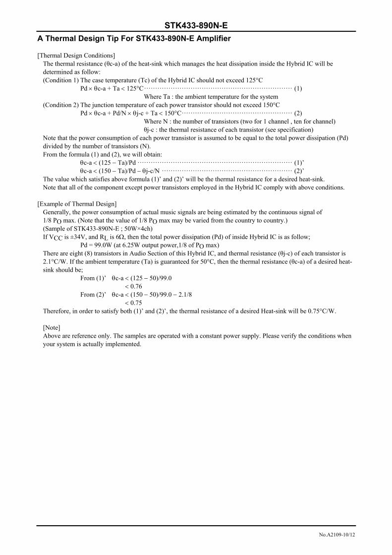
A Thermal Design Tip For STK433-890N-E Amplifier [Thermal Design Conditions]
The thermal resistance (θc-a) of the heat-sink which manages the heat dissipation inside the Hybrid IC will be determined as follow: (Condition 1) The case temperature (Tc) of the Hybrid IC should not exceed 125°C
Pd c-a + Ta 125°C ··································································· (1) Where Ta : the ambient temperature for the system
(Condition 2) The junction temperature of each power transistor should not exceed 150°C Pd c-a + Pd/N j-c + Ta 150°C ·················································· (2)
Where N : the number of transistors (two for 1 channel , ten for channel) θj-c : the thermal resistance of each transistor (see specification)
Note that the power consumption of each power transistor is assumed to be equal to the total power dissipation (Pd) divided by the number of transistors (N). From the formula (1) and (2), we will obtain:
c-a (125 Ta)/Pd ······································································ (1)’ c-a (150 Ta)/Pd j-c/N ··························································· (2)’
The value which satisfies above formula (1)’ and (2)’ will be the thermal resistance for a desired heat-sink. Note that all of the component except power transistors employed in the Hybrid IC comply with above conditions.
[Example of Thermal Design]
Generally, the power consumption of actual music signals are being estimated by the continuous signal of 1/8 PO max. (Note that the value of 1/8 PO max may be varied from the country to country.) (Sample of STK433-890N-E ; 50W×4ch) If VCC is ±34V, and RL is 6, then the total power dissipation (Pd) of inside Hybrid IC is as follow;
Pd = 99.0W (at 6.25W output power,1/8 of PO max) There are eight (8) transistors in Audio Section of this Hybrid IC, and thermal resistance (θj-c) of each transistor is 2.1°C/W. If the ambient temperature (Ta) is guaranteed for 50°C, then the thermal resistance (θc-a) of a desired heat-sink should be;
From (1)’ c-a (125 50)/99.0 0.76
From (2)’ c-a (150 50)/99.0 2.1/8 0.75
Therefore, in order to satisfy both (1)’ and (2)’, the thermal resistance of a desired Heat-sink will be 0.75°C/W. [Note] Above are reference only. The samples are operated with a constant power supply. Please verify the conditions when your system is actually implemented.
STK433-890N-E
No.A2109-11/12
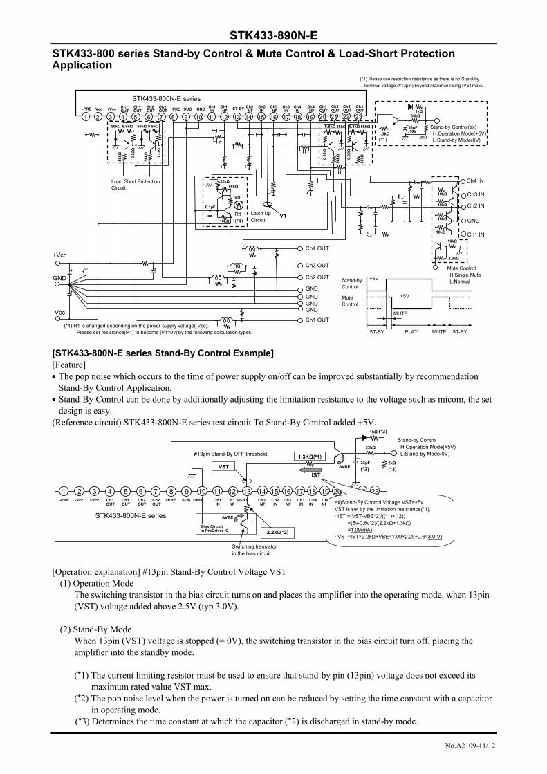
STK433-800 series Stand-by Control & Mute Control & Load-Short Protection Application [STK433-800N-E series Stand-By Control Example] [Feature] The pop noise which occurs to the time of power supply on/off can be improved substantially by recommendation
Stand-By Control Application. Stand-By Control can be done by additionally adjusting the limitation resistance to the voltage such as micom, the set
design is easy. (Reference circuit) STK433-800N-E series test circuit To Stand-By Control added +5V. [Operation explanation] #13pin Stand-By Control Voltage VST
(1) Operation Mode The switching transistor in the bias circuit turns on and places the amplifier into the operating mode, when 13pin (VST) voltage added above 2.5V (typ 3.0V).
(2) Stand-By Mode
When 13pin (VST) voltage is stopped (= 0V), the switching transistor in the bias circuit turn off, placing the amplifier into the standby mode.
(*1) The current limiting resistor must be used to ensure that stand-by pin (13pin) voltage does not exceed its
maximum rated value VST max. (*2) The pop noise level when the power is turned on can be reduced by setting the time constant with a capacitor
in operating mode. (*3) Determines the time constant at which the capacitor (*2) is discharged in stand-by mode.
(*1) Please use restriction resistance as there is no Stand-by
terminal voltage (#13pin) beyond maximun rating (VSTmax).
Stand-by Control(ex) H:Operation Mode(+5V) L:Stand-by Mode(0V)
33μF /10V
33kΩ 1kΩ
2kΩ 1.3kΩ
(*1)
STK433-800N-E series
+Vcc Ch1 IN
Ch1 NF
Ch2 IN
Ch2 NF
Ch2 OUT
Ch1 OUT -Vcc SUB GND +PRE ST-BYCh1
OUT Ch2OUT
2 3 4 5 8 7 6 9 10 11 12 13 14 15 1
-PRE Ch3 IN
Ch3 NF
16 17 18 19
Mute Control H:Single Mute L:Normal
GND
Ch1 IN
GND
+Vcc
-Vcc
Ch2 OUT
Ch1 OUT
GND
GND
Ch3 OUT
20 21 22 23
Ch3OUT
Ch4 IN
Ch4 NF
Ch3OUT
Ch4OUT
Ch4OUT
Ch4 OUT
10kΩ
10kΩ
10kΩ
2.2kΩ
10kΩ
10kΩ
Ch4 IN
GNDGND
Ch2 IN
Ch3 IN
0.2
2Ω
56kΩ
6.8kΩ
56kΩ
Latch Up Circuit 10kΩ
56kΩ
1kΩ
22kΩ
0.1μF R1 (*4)
V1
0.2
2Ω
56kΩ6.8kΩ
56kΩ
0.2
2Ω
56kΩ6.8kΩ
56kΩ
0.2
2Ω
56kΩ
6.8kΩ
56kΩ
Load Short Protection Circuit
(*4) R1 is changed depending on the power-supply voltage(-Vcc). Please set resistance(R1) to become [V1=0v] by the following calculation types.
+5V
+5V
Stand-by Control
Mute Control
ST-BY PLAY ST-BYMUTE
MUTE
Stand-by Control H:Operation Mode(+5V) L:Stand-by Mode(0V)
1.3KΩ(*1)
IST
∆VBE
1 2 3 4 7 6 5 8 9 10 11 12
STK433-800N-E series
13 14+Vcc Ch1
IN Ch1 NF
Ch2 IN
Ch2 NF
Ch2 OUT
Ch1 OUT
-Vcc SUB GND +PRE ST-BYCh1 OUT
Ch2 OUT
Bias Circuit in PreDriver IC
∆VBE
-PRE Ch3 NF
Ch4NF
Ch4IN
Ch3 IN
#13pin Stand-By OFF threshold.
VST 33μF
(*2)
33kΩ
1kΩ (*3)
2kΩ
(*3)
2.2kΩ(*2)
15 16 17 18 19 20 21 22 23Ch3OUT
Ch3OUT
Ch4OUT
Ch4OUT ex)Stand-By Control Voltage VST=+5v
VST is set by the limitation resistance(*1). · IST =(VST-VBE*2)/((*1)+(*2))
=(5v-0.6v*2)/(2.2kΩ+1.3kΩ) =1.09(mA)
· VST=IST×2.2kΩ+VBE=1.09×2.2k+0.6=3.0(V)
Switching transistor in the bias circuit
STK433-890N-E
No.A2109-12/12
ORDERING INFORMATION
Device Package Shipping (Qty / Packing)
STK433-890N-E SIP23
(Pb-Free) 25 / Bulk Box
PS
ON Semiconductor and the ON logo are registered trademarks of Semiconductor Components Industries, LLC (SCILLC). SCILLC owns the rights to a numberof patents, trademarks, copyrights, trade secrets, and other intellectual property. A listing of SCILLC’s product/patent coverage may be accessed atwww.onsemi.com/site/pdf/Patent-Marking.pdf. SCILLC reserves the right to make changes without further notice to any products herein. SCILLC makes nowarranty, representation or guarantee regarding the suitability of its products for any particular purpose, nor does SCILLC assume any liability arising out of theapplication or use of any product or circuit, and specifically disclaims any and all liability, including without limitation special, consequential or incidentaldamages. “Typical” parameters which may be provided in SCILLC data sheets and/or specifications can and do vary in different applications and actualperformance may vary over time. All operating parameters, including “Typicals” must be validated for each customer application by customer’s technicalexperts. SCILLC does not convey any license under its patent rights nor the rights of others. SCILLC products are not designed, intended, or authorized for useas components in systems intended for surgical implant into the body, or other applications intended to support or sustain life, or for any other application inwhich the failure of the SCILLC product could create a situation where personal injury or death may occur. Should Buyer purchase or use SCILLC products forany such unintended or unauthorized application, Buyer shall indemnify and hold SCILLC and its officers, employees, subsidiaries, affiliates, and distributorsharmless against all claims, costs, damages, and expenses, and reasonable attorney fees arising out of, directly or indirectly, any claim of personal injury ordeath associated with such unintended or unauthorized use, even if such claim alleges that SCILLC was negligent regarding the design or manufacture of thepart. SCILLC is an Equal Opportunity/Affirmative Action Employer. This literature is subject to all applicable copyright laws and is not for resale in any manner.