Embed Size (px)
Citation preview
NASA Tech Briefs, January 2004 13
host computer during the pixel readout,the present design reduces ROI-readouttimes to attain higher frame rates.
This camera (see figure) includes animager card consisting of a commercialCCD imager and two signal-processorchips. The imager card converts transis-tor/transistor-logic (TTL)-level signalsfrom a field programmable gate array(FPGA) controller card. These signalsare transmitted to the imager card via alow-voltage differential signaling(LVDS) cable assembly. The FPGA con-troller card is connected to the hostcomputer via a standard peripheralcomponent interface (PCI). The hostcomputer sends control parameters tothe FPGA controller card and reads
camera-status and pixel data from theFPGA controller card. Some of the op-erational parameters of the camera areprogrammable in hardware. Com-mands are loaded from the host com-puter into the FPGA controller card todefine such parameters as the framerate, integration time, and the size andlocation of an ROI.
There are two modes of operation:image capture and ROI readout. Inimage-capture mode, whole frames ofpixels are repeatedly transferred fromthe image area to the storage area of theCCD, with timing defined by the framerate and integration time registersloaded into the FPGA controller card. InROI readout, the host computer sends
commands to the FPGA controller speci-fying the size and location of an ROI inaddition to the frame rate and integra-tion time. The commands result inscrolling through unwanted lines andthrough unwanted pixels on lines untilpixels in the ROI are reached. The hostcomputer can adjust the sizes and loca-tions of the ROIs within a frame periodfor dynamic control to changes in theimage (e.g., for tracking targets).
This work was done by Steve Monacos,Angel Portillo, Gerardo Ortiz, James Alexan-der, Raymond Lam, and William Liu of Cal-tech for NASA’s Jet Propulsion Laboratory.Further information is contained in a TSP (seepage 1)NPO-30878
Stroboscope Controller for Imaging Helicopter RotorsThis unit can be programmed to operate in a variety of configurations.Ames Research Center, Moffett Field, California
A versatile electronic timing-and-con-trol unit, denoted a rotorcraft strobecontroller, has been developed for usein controlling stroboscopes, lasers, videocameras, and other instruments for cap-turing still images of rotating machineparts — especially helicopter rotors.This unit is designed to be compatiblewith a variety of sources of input shaft-angle or timing signals and to be capa-ble of generating a variety of output sig-nals suitable for triggering instrumentscharacterized by different input-signalspecifications. It is also designed to beflexible and reconfigurable in that it canbe modified and updated throughchanges in its control software, withoutneed to change its hardware.
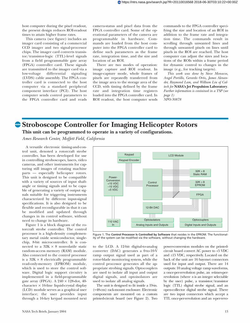
Figure 1 is a block diagram of the ro-torcraft strobe controller. The controlprocessor is a high-density complemen-tary metal oxide semiconductor, single-chip, 8-bit microcontroller. It is con-nected to a 32K × 8 nonvolatile staticrandom-access memory (RAM) module.Also connected to the control processoris a 32K × 8 electrically programmableread-only-memory (EPROM) module,which is used to store the control soft-ware. Digital logic support circuitry isimplemented in a field-programmablegate array (FPGA). A 240 × 128-dot, 40-character × 16-line liquid-crystal display(LCD) module serves as a graphical userinterface; the user provides inputthrough a 16-key keypad mounted next
to the LCD. A 12-bit digital-to-analogconverter (DAC) generates a 0-to-10-Vramp output signal used as part of arotor-blade monitoring system, while thecontrol processor generates all the ap-propriate strobing signals. Optocouplersare used to isolate all input and outputdigital signals, and optoisolators areused to isolate all analog signals.
The unit is designed to fit inside a 19-in.(≈48-cm) rack-mount enclosure. Electroniccomponents are mounted on a customprinted-circuit board (see Figure 2). Two
power-conversion modules on the printed-circuit board convert AC power to +5 VDCand ±15 VDC, respectively. Located on theback of the unit are 16 bayonet connectorsused for input and output. There are 14outputs: 10 analog voltage ramp waveforms,a once-per-revolution pulse, an n-times-per-revolution (where n is an integer selectableby the user) pulse, a transistor/transistorlogic (TTL) digital strobe signal, and anopen-collector digital strobe signal. Thereare two input connectors which accept aTTL once-per-revolution and an n-per-revo-
Keypad LCD Module
Keypad Encoder
Power-Conversion+15 VDC–15 VDC+5 VDC
110 VACIn
ControlProcessor
12-Bit DAC
Optoisolators
Analog Inputs and Outputs
Optocouplers
Digital Inputs and Outputs
32K × 8Static RAM
32K × 8EPROM
FPGA
Figure 1. The Control Processor Is Controlled by Software that resides in the EPROM. The functional-ity of the system can be modified via the software, without changing the hardware.
https://ntrs.nasa.gov/search.jsp?R=20110016568 2018-06-30T03:10:22+00:00Z

14 NASA Tech Briefs, January 2004
lution signal. They can be either single-ended, floating, or differential.
The control software was written in theC language. The main functions of the soft-ware are to read data present on the con-trol-processor ports, generate the strobesignals, generate the ramp informationused to monitor rotor-blade parameters bywriting to the 12-bit DAC, save and retrieveconfiguration settings to and from thenonvolatile RAM, communicate with theFPGA, accept keypad input, and controland update the LCD by paging though ap-propriate user selections and menus. Theuser can gain access to several menus to setsuch parameters as the number of bladesto track, the blade-offset angle, and thenumber of pulses per revolution.
This work was completed for Jon Lauten-schlager of the U.S. Army Aviation and Mis-sile Command by Scott Jensen, John Marmie,and Nghia Mai of Ames Research Center.Further information is contained in a TSP(see page 1)
Inquiries concerning rights for the commer-cial use of this invention should be addressedto the Patent Counsel, Ames Research Center,(650) 604-5104. Refer to ARC-14966.
19"
Figure 2. The Rack-Mount Enclosure was photographed from above and behind with the cover re-moved to show components mounted on the printed-circuit board.