Embed Size (px)
Citation preview
www.sciencemag.org/cgi/content/full/science.1222360/DC1
Supplementary Materials for
Signatures of Majorana Fermions in Hybrid Superconductor-Semiconductor Nanowire Devices
V. Mourik, K. Zuo, S. M. Frolov, S. R. Plissard, E. P. A. M. Bakkers, L. P. Kouwenhoven*
*To whom correspondence should be addressed. E-mail: [email protected]
Published 12 April 2012 on Science Express
DOI: 10.1126/science.1222360
This PDF file includes:
Supplementary Text Figs. S1 to S14 Full Reference List
Other Supplementary Material for this manuscript includes the following: (available at www.sciencemag.org/cgi/content/full/science.1222360/DC1)
Data Files as a zipped archives: 1222360raw_majorana.zip Raw data files underlying figures in the paper, in text (ASCII) format. Data format is described in readme.txt file included in the archive. All questions on this material should be addressed to the authors.
Supplementary Materials:
Signatures of Majorana fermions in hybrid superconductor‐semiconductor nanowire devices
V. Mourik, K. Zuo, S.M. Frolov, S.R. Plissard, E.P.A.M. Bakkers and L.P. Kouwenhoven
1
Summary of Supplementary Figures
Below we provide details of nanowire sample fabrication as well as supporting measurements from multiple devices. The main observations of the paper, i.e. zero‐bias peak (ZBP) that appears at finite magnetic field and persists over a significant range of field and gate voltages, are reproduced in three N‐NW‐S devices measured in two setups (Figs. S1, S3, S6, S7, S10, S11). Furthermore we demonstrate S‐NW‐S devices and N‐NW‐N devices (Figs. S12‐S14). In S‐NW‐S devices persistent zero‐bias peaks are also observed, however they cannot be distinguished from Josephson supercurrents. In N‐NW‐N devices zero‐bias peaks are also observed for a small range of gate voltages (Fig. S13, S14), however only when gate‐and field‐tunable states pass through zero bias. This indicates that superconductivity is a required ingredient for the observation of a persistent zero‐bias peak.
Specifically, we present more examples of magnetic field dependences of the zero bias peak in N‐NW‐S devices (Figs. S3, S6, S7, S10). These data establish the magnetic field range of the zero‐bias peak from ~70 mT and up to 1.0 T (varying for different gate settings). Additional gate dependences investigate the splitting of the zero‐bias peak (Figs. S4, S5). Examples of tunnel barrier gate dependences are provided in Figs. S9 and S11. Finally, other features that occur at zero bias are studied in Figs. S2 and S8. In Fig. S2 we identify Andreev bound states confined in the nanowire segment covered by the superconductor. In Fig. S8 we investigate zero‐bias peaks observed at zero magnetic field.
Author contributions. L.P.K. and S.M.F. supervised the experiments; S.R.P. and E.P.A.M.B. grew the nanowires; V.M. and K.Z. fabricated nanowire devices; V.M., K.Z. and S.M.F. performed the measurements; V.M., K.Z., S.M.F. and L.P.K. analyzed the data; the manuscript has been prepared with contributions from all authors.
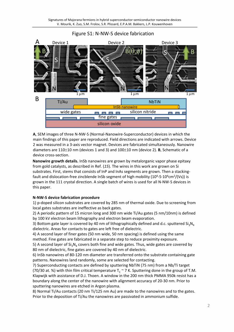
Figure S1: N‐NW‐S device fabrication
S
N
S
N
S
N
Device 1 Device 2 Device 3
A, SEM images of three N‐NW‐S (Normal‐Nanowire‐Superconductor) devices in which the main findings of this paper are reproduced. Field directions are indicated with arrows. Device 2 was measured in a 3‐axis vector magnet. Devices are fabricated simultaneously. Nanowire diameters are 11010 nm (devices 1 and 3) and 10010 nm (device 2). B, Schematic of a device cross‐section.
1 m 1 m 1 m
2
Signatures of Majorana fermions in hybrid superconductor‐semiconductor nanowire devicesV. Mourik, K. Zuo, S.M. Frolov, S.R. Plissard, E.P.A.M. Bakkers, L.P. Kouwenhoven
Nanowire growth details. InSb nanowires are grown by metalorganic vapor phase epitaxy from gold catalysts, as described in Ref. (15). The wires in this work are grown on Si substrates. First, stems that consists of InP and InAs segments are grown. Then a stacking‐fault and dislocation‐free zincblende InSb segment of high mobility (104‐5∙104cm2/(Vs)) is grown in the 111 crystal direction. A single batch of wires is used for all N‐NW‐S devices in this paper.
N‐NW‐S device fabrication procedure1) p‐doped silicon substrates are covered by 285 nm of thermal oxide. Due to screening from local gates substrates are ineffective as back gates.2) A periodic pattern of 15 micron long and 300 nm wide Ti/Au gates (5 nm/10nm) is defined by 100 kV electron beam lithography and electron beam evaporation.3) Bottom gate layer is covered by 40 nm of lithographically defined and d.c. sputtered Si3N4
dielectric. Areas for contacts to gates are left free of dielectric.4) A second layer of finer gates (50 nm wide, 50 nm spacing) is defined using the same method. Fine gates are fabricated in a separate step to reduce proximity exposure.5) A second layer of Si3N4 covers both fine and wide gates. Thus, wide gates are covered by 80 nm of dielectric, fine gates are covered by 40 nm of dielectric.6) InSb nanowires of 80‐120 nm diameter are transferred onto the substrate containing gate patterns. Nanowires land randomly, some are selected for contacting.7) Superconducting contacts are defined by sputtering NbTiN (75 nm) from a Nb/Ti target (70/30 at. %) with thin film critical temperature TC ~ 7 K. Sputtering done in the group of T.M. Klapwijk with assistance of D.J. Thoen. A window in the 200 nm thick PMMA 950k resist has a boundary along the center of the nanowire with alignment accuracy of 20‐30 nm. Prior to sputtering nanowires are etched in Argon plasma.8) Normal Ti/Au contacts (20 nm Ti/125 nm Au) are made to the nanowires and to the gates. Prior to the deposition of Ti/Au the nanowires are passivated in ammonium sulfide.
NbTiNTi/AuInSb nanowire
silicon oxide
silicon nitridewide gatesfine gates
B BB()A
B
Gate 2 (V)‐5.0 7.5
dI/dV (2e2/h)
0.1
0.5
V (mV)
0
‐4
4
2
‐2
B (T)0 0.5 1.5 2.0
V (mV)
0
‐2
2
1
‐1
dI/dV (2e2/h)
0.1
0.5
Gate 4 (V)‐5.0 ‐3.0
Gate 2 (V)
‐5.5
‐3.0 dI/dV (2e2/h)
0.25
0.45
0.1
0.2
0.3
0.4
0.5
-4 -2 0 2 4
Gate 2 = -7.2 V
V (mV)
dI/d
V (
2e2/h
)
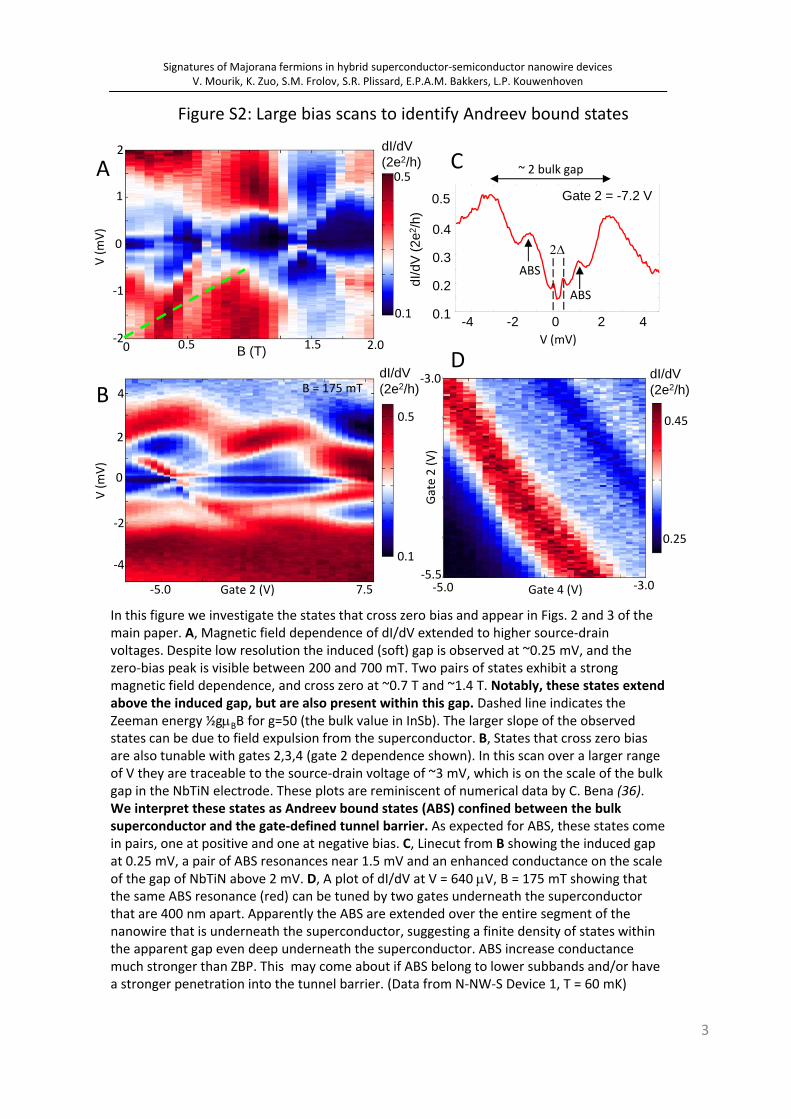
Figure S2: Large bias scans to identify Andreev bound states
In this figure we investigate the states that cross zero bias and appear in Figs. 2 and 3 of the main paper. A, Magnetic field dependence of dI/dV extended to higher source‐drain voltages. Despite low resolution the induced (soft) gap is observed at ~0.25 mV, and the zero‐bias peak is visible between 200 and 700 mT. Two pairs of states exhibit a strong magnetic field dependence, and cross zero at ~0.7 T and ~1.4 T. Notably, these states extend above the induced gap, but are also present within this gap. Dashed line indicates the Zeeman energy ½gBB for g=50 (the bulk value in InSb). The larger slope of the observed states can be due to field expulsion from the superconductor. B, States that cross zero bias are also tunable with gates 2,3,4 (gate 2 dependence shown). In this scan over a larger range of V they are traceable to the source‐drain voltage of ~3 mV, which is on the scale of the bulk gap in the NbTiN electrode. These plots are reminiscent of numerical data by C. Bena (36). We interpret these states as Andreev bound states (ABS) confined between the bulk superconductor and the gate‐defined tunnel barrier. As expected for ABS, these states come in pairs, one at positive and one at negative bias. C, Linecut from B showing the induced gap at 0.25 mV, a pair of ABS resonances near 1.5 mV and an enhanced conductance on the scale of the gap of NbTiN above 2 mV. D, A plot of dI/dV at V = 640 V, B = 175 mT showing that the same ABS resonance (red) can be tuned by two gates underneath the superconductor that are 400 nm apart. Apparently the ABS are extended over the entire segment of the nanowire that is underneath the superconductor, suggesting a finite density of states within the apparent gap even deep underneath the superconductor. ABS increase conductance much stronger than ZBP. This may come about if ABS belong to lower subbands and/or have a stronger penetration into the tunnel barrier. (Data from N‐NW‐S Device 1, T = 60 mK)
A
B
C
D
ABS
ABS
~ 2 bulk gap
3
B = 175 mT
Signatures of Majorana fermions in hybrid superconductor‐semiconductor nanowire devicesV. Mourik, K. Zuo, S.M. Frolov, S.R. Plissard, E.P.A.M. Bakkers, L.P. Kouwenhoven
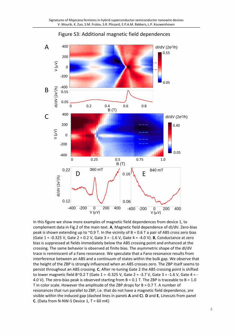
Figure S3: Additional magnetic field dependences
0.05
0.55
0 0.2 0.4 0.6 0.8
V (V
)
0
‐400
400
200
‐200
dI/dV (2e2/h)
B (T)
dI/dV (2e2/h)
0.05
0.55V (V
)
0
‐400
400
200
‐200
B (T)0 0.25 0.5 0.75 1.0
dI/dV (2e2/h)
0.05
0.40
In this figure we show more examples of magnetic field dependences from device 1, to complement data in Fig.2 of the main text. A, Magnetic field dependence of dI/dV. Zero‐bias peak is shown extending up to ~0.9 T. In the vicinity of B = 0.6 T a pair of ABS cross zero bias (Gate 1 = ‐0.325 V, Gate 2 = 0.2 V, Gate 3 = ‐1.6 V, Gate 4 = ‐4.0 V). B, Conductance at zero bias is suppressed at fields immediately below the ABS crossing point and enhanced at the crossing. The same behavior is observed at finite bias. The asymmetric shape of the dI/dV trace is reminiscent of a Fano resonance. We speculate that a Fano resonance results from interference between an ABS and a continuum of states within the bulk gap. We observe that the height of the ZBP is strongly influenced when an ABS crosses zero. The ZBP itself seems to persist throughout an ABS crossing. C, After re‐tuning Gate 2 the ABS crossing point is shifted to lower magnetic field B~0.2 T (Gate 1 = ‐0.325 V, Gate 2 = ‐3.7 V, Gate 3 = ‐1.6 V, Gate 4 = ‐4.0 V). The zero‐bias peak is observed starting from B = 0.1 T. The ZBP is traceable to B = 1.0 T in color scale. However the amplitude of the ZBP drops for B > 0.7 T. A number of resonances that run parallel to ZBP, i.e. that do not have a magnetic field dependence, are visible within the induced gap (dashed lines in panels A and C). D and E, Linecuts from panel C. (Data from N‐NW‐S Device 1, T = 60 mK)
A
B
C
4
0.12
0.22
-400 -200 0 200 400
360 mT
0.06
0.16
-400 -200 0 200 400
840 mT
dI/dV (2e2/h)
V (V) V (V)
D E
Signatures of Majorana fermions in hybrid superconductor‐semiconductor nanowire devicesV. Mourik, K. Zuo, S.M. Frolov, S.R. Plissard, E.P.A.M. Bakkers, L.P. Kouwenhoven
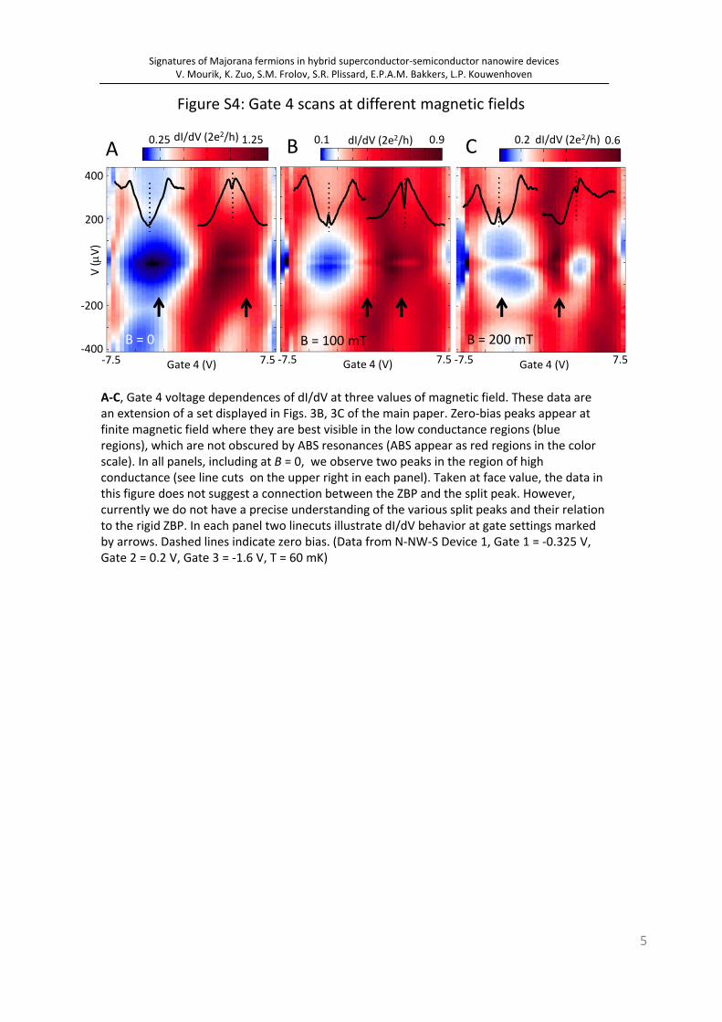
Figure S4: Gate 4 scans at different magnetic fields
Gate 4 (V)‐7.5 7.5 Gate 4 (V)‐7.5 7.5 Gate 4 (V)‐7.5 7.5
V (V
)
‐400
400
200
‐200
dI/dV (2e2/h) 1.250.25 0.90.1 0.60.2dI/dV (2e2/h) dI/dV (2e2/h)
A‐C, Gate 4 voltage dependences of dI/dV at three values of magnetic field. These data are an extension of a set displayed in Figs. 3B, 3C of the main paper. Zero‐bias peaks appear at finite magnetic field where they are best visible in the low conductance regions (blue regions), which are not obscured by ABS resonances (ABS appear as red regions in the color scale). In all panels, including at B = 0, we observe two peaks in the region of high conductance (see line cuts on the upper right in each panel). Taken at face value, the data in this figure does not suggest a connection between the ZBP and the split peak. However, currently we do not have a precise understanding of the various split peaks and their relation to the rigid ZBP. In each panel two linecuts illustrate dI/dV behavior at gate settings marked by arrows. Dashed lines indicate zero bias. (Data from N‐NW‐S Device 1, Gate 1 = ‐0.325 V, Gate 2 = 0.2 V, Gate 3 = ‐1.6 V, T = 60 mK)
A B C
B = 200 mTB = 100 mTB = 0
5
Signatures of Majorana fermions in hybrid superconductor‐semiconductor nanowire devicesV. Mourik, K. Zuo, S.M. Frolov, S.R. Plissard, E.P.A.M. Bakkers, L.P. Kouwenhoven
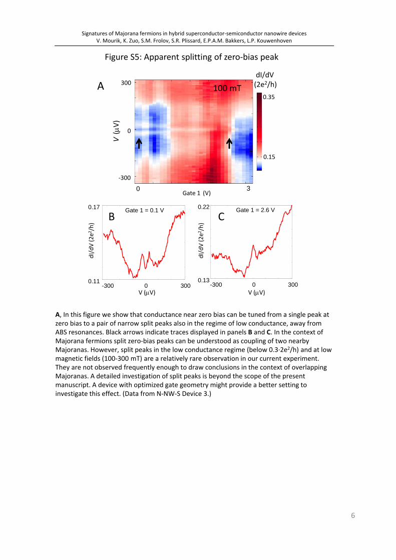
Figure S5: Apparent splitting of zero‐bias peak
A, In this figure we show that conductance near zero bias can be tuned from a single peak at zero bias to a pair of narrow split peaks also in the regime of low conductance, away from ABS resonances. Black arrows indicate traces displayed in panels B and C. In the context of Majorana fermions split zero‐bias peaks can be understood as coupling of two nearby Majoranas. However, split peaks in the low conductance regime (below 0.3∙2e2/h) and at low magnetic fields (100‐300 mT) are a relatively rare observation in our current experiment. They are not observed frequently enough to draw conclusions in the context of overlapping Majoranas. A detailed investigation of split peaks is beyond the scope of the present manuscript. A device with optimized gate geometry might provide a better setting to investigate this effect. (Data from N‐NW‐S Device 3.)
6
0 3Gate 1 (V)
dI/dV (2e2/h)300
0
V(V)
‐300
0.15
0.35
Signatures of Majorana fermions in hybrid superconductor‐semiconductor nanowire devicesV. Mourik, K. Zuo, S.M. Frolov, S.R. Plissard, E.P.A.M. Bakkers, L.P. Kouwenhoven
0.11
0.17
-300 0 300
Gate 1 = 0.1 V
0.13
0.22
-300 0 300
Gate 1 = 2.6 V
dI/dV(2e2/h)
dI/dV(2e2/h)
V (V) V (V)
A
B C
100 mT
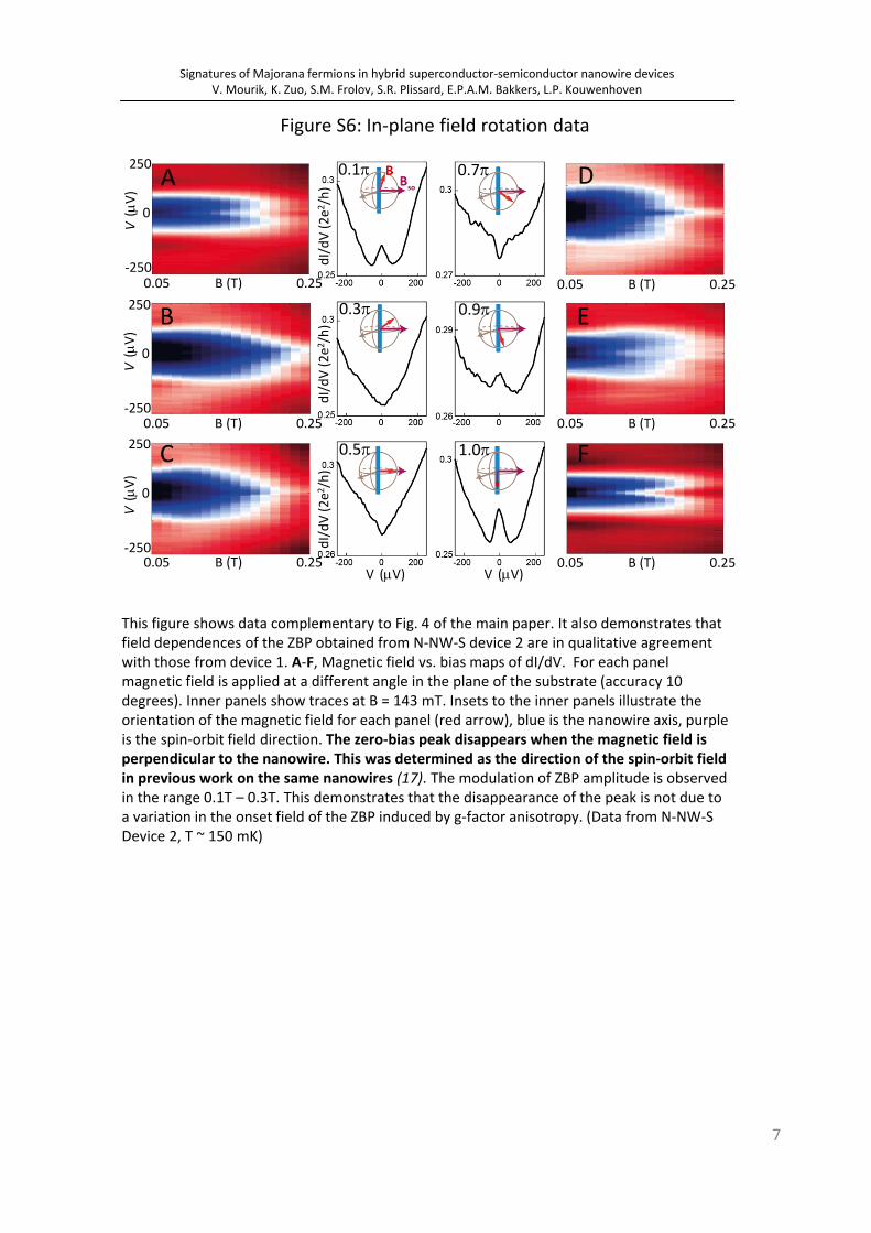
Figure S6: In‐plane field rotation data
7
V(V)
0
250
‐250B (T)0.05 0.25
V (V) V (V)
B (T)0.05 0.25
B (T)0.05 0.25
V(V)
0
250
‐250
V(V)
0
250
‐250
dI/dV(2e2/h)
dI/dV(2e2/h)
dI/dV(2e2/h)
B (T)0.05 0.25
B (T)0.05 0.25
B (T)0.05 0.25
A
B
C
D
E
F
This figure shows data complementary to Fig. 4 of the main paper. It also demonstrates that field dependences of the ZBP obtained from N‐NW‐S device 2 are in qualitative agreement with those from device 1. A‐F, Magnetic field vs. bias maps of dI/dV. For each panel magnetic field is applied at a different angle in the plane of the substrate (accuracy 10 degrees). Inner panels show traces at B = 143 mT. Insets to the inner panels illustrate the orientation of the magnetic field for each panel (red arrow), blue is the nanowire axis, purple is the spin‐orbit field direction. The zero‐bias peak disappears when the magnetic field is perpendicular to the nanowire. This was determined as the direction of the spin‐orbit field in previous work on the same nanowires (17). The modulation of ZBP amplitude is observed in the range 0.1T – 0.3T. This demonstrates that the disappearance of the peak is not due to a variation in the onset field of the ZBP induced by g‐factor anisotropy. (Data from N‐NW‐S Device 2, T ~ 150 mK)
Signatures of Majorana fermions in hybrid superconductor‐semiconductor nanowire devicesV. Mourik, K. Zuo, S.M. Frolov, S.R. Plissard, E.P.A.M. Bakkers, L.P. Kouwenhoven
0.1
0.3
0.5
0.7
0.9
1.0
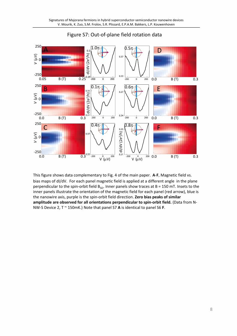
Figure S7: Out‐of‐plane field rotation data
8
V(V)
0
250
‐250B (T)0.05 0.25
V (V) V (V)
B (T)0.0 0.3
B (T)0.0 0.3
V(V)
0
250
‐250
V(V)
0
250
‐250
dI/dV(2e2/h)
dI/dV(2e2/h)
dI/dV(2e2/h)
B (T)0.0 0.3
B (T)0.0 0.3
B (T)0.0 0.3
A
B
C
D
E
F
This figure shows data complementary to Fig. 4 of the main paper. A‐F, Magnetic field vs.
bias maps of dI/dV. For each panel magnetic field is applied at a different angle in the plane perpendicular to the spin‐orbit field BSO. Inner panels show traces at B = 150 mT. Insets to the inner panels illustrate the orientation of the magnetic field for each panel (red arrow), blue is the nanowire axis, purple is the spin‐orbit field direction. Zero bias peaks of similar amplitude are observed for all orientations perpendicular to spin‐orbit field. (Data from N‐NW‐S Device 2, T ~ 150mK.) Note that panel S7 A is identical to panel S6 F.
Signatures of Majorana fermions in hybrid superconductor‐semiconductor nanowire devicesV. Mourik, K. Zuo, S.M. Frolov, S.R. Plissard, E.P.A.M. Bakkers, L.P. Kouwenhoven
1.0
0.1
0.4
0.5
0.6
0.8
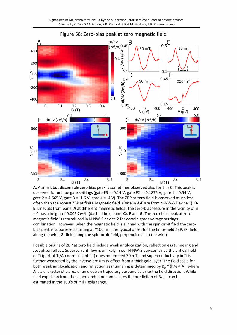
Figure S8: Zero‐bias peak at zero magnetic fieldV (V
)
‐400
400
200
‐200
dI/dV(2e2/h)
0.1
0.4
B (T)0 0.1 0.2 0.3 0.4
0.1
0.45-30 mT
0.1
0.510 mT
0.05
0.4 90 mT
0.15
0.45250 mT
dI/dV (2e2/h
dI/dV (2e2/h)
‐400 400V (V)
‐400 400V (V)
0 0
dI/dV (2e2/h) dI/dV (2e2/h)
‐300
300
0
V (V
)
0
‐300
300
0
V (V
)
B (T)0 0.1 0.2 0.3
B (T)0 0.1 0.2 0.3
0.4 0.5 0.4 0.5
A
A, A small, but discernible zero bias peak is sometimes observed also for B 0. This peak is observed for unique gate settings (gate F3 = ‐0.14 V, gate F2 = ‐0.1875 V, gate 1 = 0.54 V, gate 2 = 4.665 V, gate 3 = ‐1.6 V, gate 4 = ‐4 V). The ZBP at zero field is observed much less often than the robust ZBP at finite magnetic field. (Data in A‐E are from N‐NW‐S Device 1). B‐E, Linecuts from panel A at different magnetic fields. The zero‐bias feature in the vicinity of B = 0 has a height of 0.005∙2e2/h (dashed box, panel C). F and G, The zero‐bias peak at zero magnetic field is reproduced in N‐NW‐S device 2 for certain gates voltage settings combination. However, when the magnetic field is aligned with the spin‐orbit field the zero‐bias peak is suppressed starting at ~100 mT, the typical onset for the finite‐field ZBP. (F: field along the wire, G: field along the spin‐orbit field, perpendicular to the wire).
Possible origins of ZBP at zero field include weak antilocalization, reflectionless tunneling and Josephson effect. Supercurrent flow is unlikely in our N‐NW‐S devices, since the critical field of Ti (part of Ti/Au normal contact) does not exceed 30 mT, and superconductivity in Ti is further weakened by the inverse proximity effect from a thick gold layer. The field scale for both weak antilocalization and reflectionless tunneling is determined by B0 ~ (h/e)/(A), where A is a characteristic area of an electron trajectory perpendicular to the field direction. While field expulsion from the superconductor complicates the prediction of B0 , it can be estimated in the 100’s of milliTesla range.
B C
D E
F G
9
Signatures of Majorana fermions in hybrid superconductor‐semiconductor nanowire devicesV. Mourik, K. Zuo, S.M. Frolov, S.R. Plissard, E.P.A.M. Bakkers, L.P. Kouwenhoven
B
BSO BBSO
ANbTiNTi/Au
nanowire
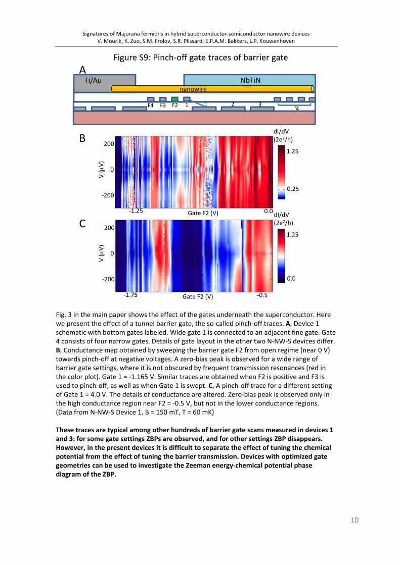
Figure S9: Pinch‐off gate traces of barrier gate
dI/dV (2e2/h)
0.25
1.25
dI/dV (2e2/h)
0.0
1.25
V (V
)
0
V (V
)
0
200
‐200
200
‐200
Gate F2 (V)‐1.25 0.0
Gate F2 (V)‐1.75 ‐0.5
Fig. 3 in the main paper shows the effect of the gates underneath the superconductor. Here we present the effect of a tunnel barrier gate, the so‐called pinch‐off traces. A, Device 1 schematic with bottom gates labeled. Wide gate 1 is connected to an adjacent fine gate. Gate 4 consists of four narrow gates. Details of gate layout in the other two N‐NW‐S devices differ. B, Conductance map obtained by sweeping the barrier gate F2 from open regime (near 0 V) towards pinch‐off at negative voltages. A zero‐bias peak is observed for a wide range of barrier gate settings, where it is not obscured by frequent transmission resonances (red in the color plot). Gate 1 = ‐1.165 V. Similar traces are obtained when F2 is positive and F3 is used to pinch‐off, as well as when Gate 1 is swept. C, A pinch‐off trace for a different setting of Gate 1 = 4.0 V. The details of conductance are altered. Zero‐bias peak is observed only in the high conductance region near F2 = ‐0.5 V, but not in the lower conductance regions. (Data from N‐NW‐S Device 1, B = 150 mT, T = 60 mK)
These traces are typical among other hundreds of barrier gate scans measured in devices 1 and 3: for some gate settings ZBPs are observed, and for other settings ZBP disappears. However, in the present devices it is difficult to separate the effect of tuning the chemical potential from the effect of tuning the barrier transmission. Devices with optimized gate geometries can be used to investigate the Zeeman energy‐chemical potential phase diagram of the ZBP.
B
C
10
1F2F3F4 1 2 34
Signatures of Majorana fermions in hybrid superconductor‐semiconductor nanowire devicesV. Mourik, K. Zuo, S.M. Frolov, S.R. Plissard, E.P.A.M. Bakkers, L.P. Kouwenhoven
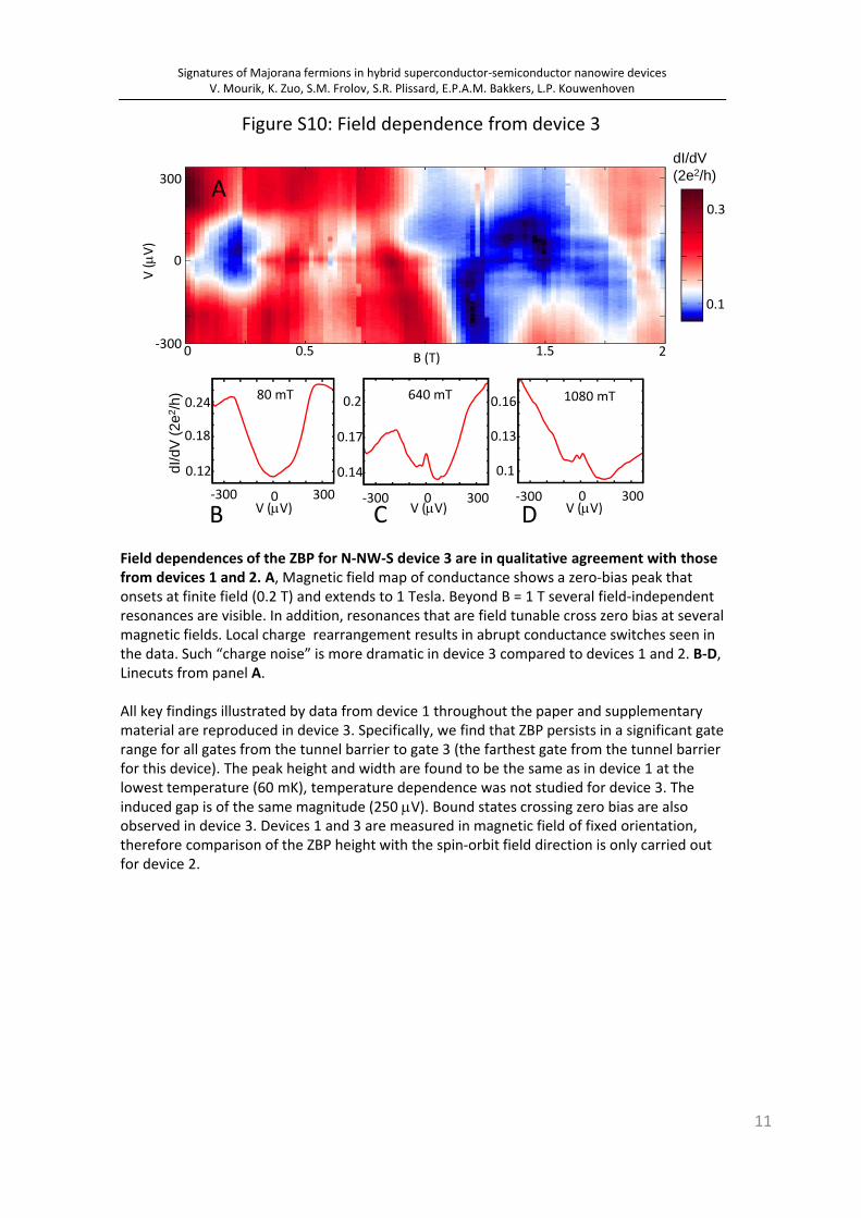
Figure S10: Field dependence from device 3
0.14
0.17
0.2
‐300 0 300
640 mT
0.12
0.18
0.24
‐300 0 300
0.1
0.13
0.16
‐300 0 300
80 mT 1080 mT
‐300
300
0
V (V
)
dI/d
V (
2e2/h
)
V (V) V (V) V (V)
dI/dV(2e2/h)
0.1
0.3
Field dependences of the ZBP for N‐NW‐S device 3 are in qualitative agreement with those from devices 1 and 2. A, Magnetic field map of conductance shows a zero‐bias peak that onsets at finite field (0.2 T) and extends to 1 Tesla. Beyond B = 1 T several field‐independent resonances are visible. In addition, resonances that are field tunable cross zero bias at several magnetic fields. Local charge rearrangement results in abrupt conductance switches seen in the data. Such “charge noise” is more dramatic in device 3 compared to devices 1 and 2. B‐D, Linecuts from panel A.
All key findings illustrated by data from device 1 throughout the paper and supplementary material are reproduced in device 3. Specifically, we find that ZBP persists in a significant gate range for all gates from the tunnel barrier to gate 3 (the farthest gate from the tunnel barrier for this device). The peak height and width are found to be the same as in device 1 at the lowest temperature (60 mK), temperature dependence was not studied for device 3. The induced gap is of the same magnitude (250 V). Bound states crossing zero bias are also observed in device 3. Devices 1 and 3 are measured in magnetic field of fixed orientation, therefore comparison of the ZBP height with the spin‐orbit field direction is only carried out for device 2.
A
B C D
11
Signatures of Majorana fermions in hybrid superconductor‐semiconductor nanowire devicesV. Mourik, K. Zuo, S.M. Frolov, S.R. Plissard, E.P.A.M. Bakkers, L.P. Kouwenhoven
B (T)0 20.5 1.5
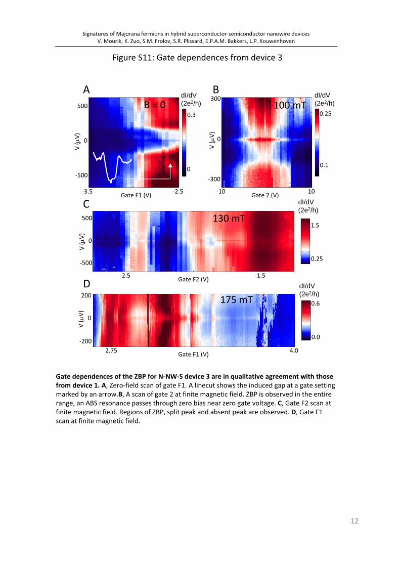
Figure S11: Gate dependences from device 3
Gate dependences of the ZBP for N‐NW‐S device 3 are in qualitative agreement with those from device 1. A, Zero‐field scan of gate F1. A linecut shows the induced gap at a gate setting marked by an arrow.B, A scan of gate 2 at finite magnetic field. ZBP is observed in the entire range, an ABS resonance passes through zero bias near zero gate voltage. C, Gate F2 scan at finite magnetic field. Regions of ZBP, split peak and absent peak are observed. D, Gate F1 scan at finite magnetic field.
A
12
Signatures of Majorana fermions in hybrid superconductor‐semiconductor nanowire devicesV. Mourik, K. Zuo, S.M. Frolov, S.R. Plissard, E.P.A.M. Bakkers, L.P. Kouwenhoven
‐500
500
V (V
)
0
Gate F1 (V)‐3.5 ‐2.5
dI/dV(2e2/h)
0
0.3
B
‐300
300
V (V
)
0
dI/dV(2e2/h)
0.1
0.25
Gate 2 (V)‐10 10
C
D
‐500
500
V (V
)
0
Gate F2 (V)‐2.5 ‐1.5
dI/dV(2e2/h)
0.25
1.5
B = 0 100 mT
Gate F1 (V)2.75 4.0
‐200
200
V (V
)
0
dI/dV(2e2/h)
0.0
0.6
130 mT
175 mT
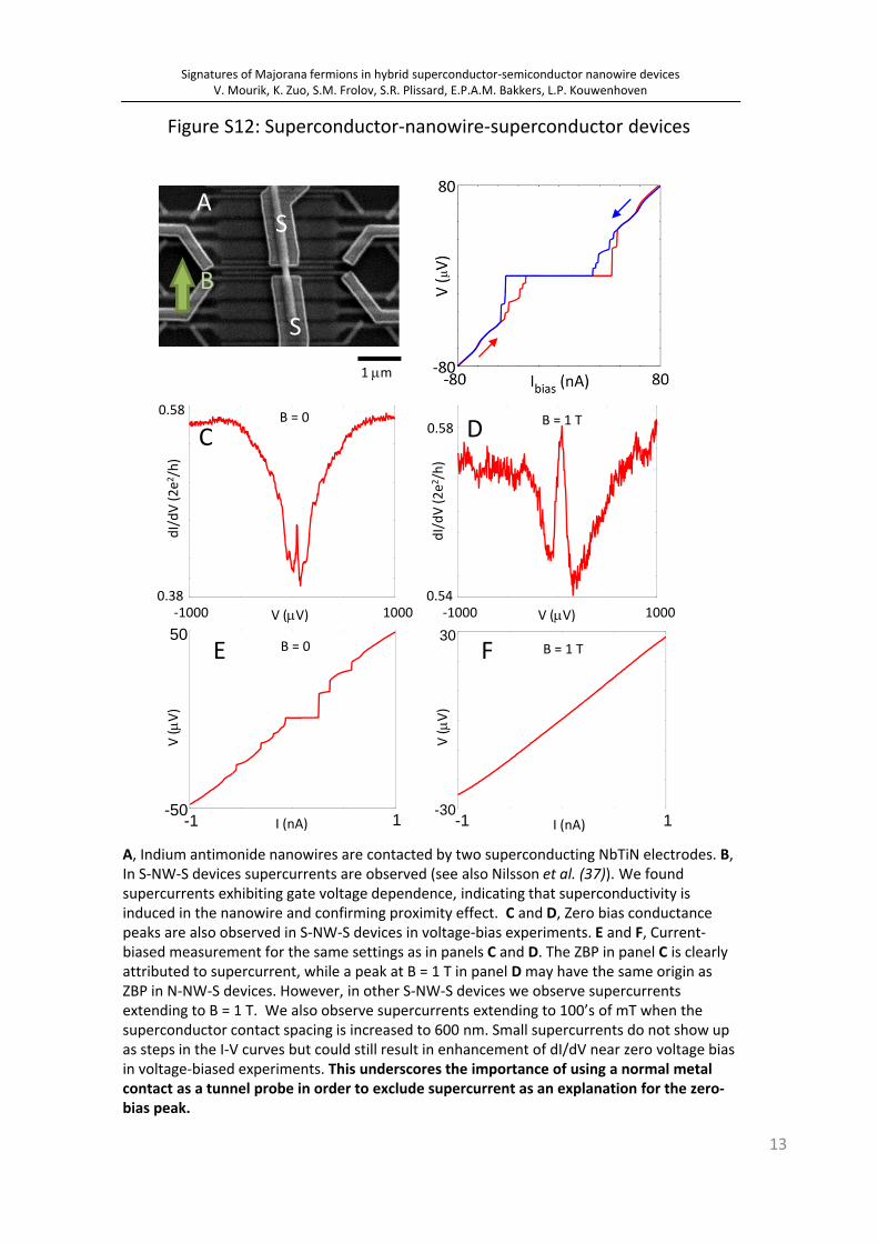
Figure S12: Superconductor‐nanowire‐superconductor devices
0.38
0.58
‐1000 10000.54
0.58
‐1000 1000
dI/dV(2e2/h)
dI/dV(2e2/h)
V (V) V (V)
V (V
)
V (V
)
I (nA) I (nA)-50
50
-1 1-30
30
1-1
1 m
A, Indium antimonide nanowires are contacted by two superconducting NbTiN electrodes. B, In S‐NW‐S devices supercurrents are observed (see also Nilsson et al. (37)). We found supercurrents exhibiting gate voltage dependence, indicating that superconductivity is induced in the nanowire and confirming proximity effect. C and D, Zero bias conductance peaks are also observed in S‐NW‐S devices in voltage‐bias experiments. E and F, Current‐biased measurement for the same settings as in panels C and D. The ZBP in panel C is clearly attributed to supercurrent, while a peak at B = 1 T in panel Dmay have the same origin as ZBP in N‐NW‐S devices. However, in other S‐NW‐S devices we observe supercurrents extending to B = 1 T. We also observe supercurrents extending to 100’s of mT when the superconductor contact spacing is increased to 600 nm. Small supercurrents do not show up as steps in the I‐V curves but could still result in enhancement of dI/dV near zero voltage bias in voltage‐biased experiments. This underscores the importance of using a normal metal contact as a tunnel probe in order to exclude supercurrent as an explanation for the zero‐bias peak.
A B
C D
E F
B = 0
B = 0
B = 1 T
B = 1 T
13
S
S
Signatures of Majorana fermions in hybrid superconductor‐semiconductor nanowire devicesV. Mourik, K. Zuo, S.M. Frolov, S.R. Plissard, E.P.A.M. Bakkers, L.P. Kouwenhoven
B
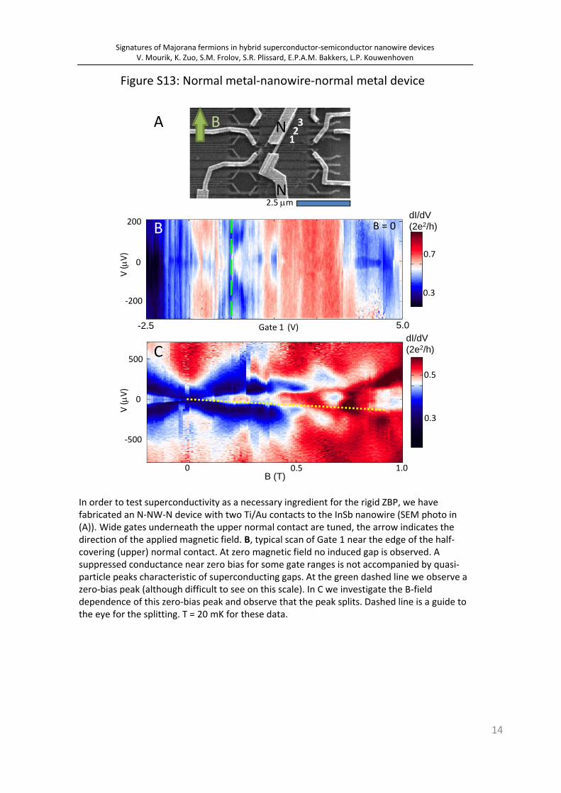
Figure S13: Normal metal‐nanowire‐normal metal device
14
Signatures of Majorana fermions in hybrid superconductor‐semiconductor nanowire devicesV. Mourik, K. Zuo, S.M. Frolov, S.R. Plissard, E.P.A.M. Bakkers, L.P. Kouwenhoven
‐200
200
0
V (V
)
‐500
500
0
V (V
)
-2.5 5.0Gate 1 (V)
B (T)0 0.5 1.0
dI/dV(2e2/h)
0.3
0.7
dI/dV(2e2/h)
0.3
0.5
B
A
C
In order to test superconductivity as a necessary ingredient for the rigid ZBP, we have fabricated an N‐NW‐N device with two Ti/Au contacts to the InSb nanowire (SEM photo in (A)). Wide gates underneath the upper normal contact are tuned, the arrow indicates the direction of the applied magnetic field. B, typical scan of Gate 1 near the edge of the half‐covering (upper) normal contact. At zero magnetic field no induced gap is observed. A suppressed conductance near zero bias for some gate ranges is not accompanied by quasi‐particle peaks characteristic of superconducting gaps. At the green dashed line we observe a zero‐bias peak (although difficult to see on this scale). In C we investigate the B‐field dependence of this zero‐bias peak and observe that the peak splits. Dashed line is a guide to the eye for the splitting. T = 20 mK for these data.
2.5 mN
N
B = 0
B123
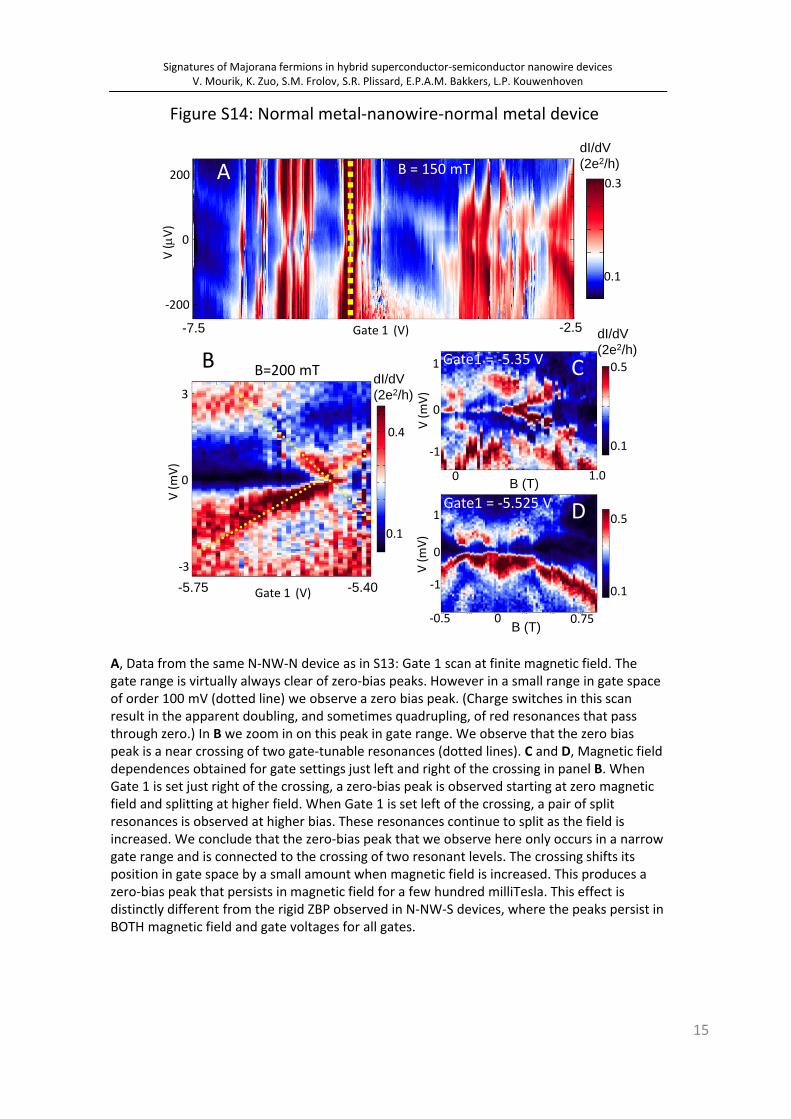
Figure S14: Normal metal‐nanowire‐normal metal device
15
Signatures of Majorana fermions in hybrid superconductor‐semiconductor nanowire devicesV. Mourik, K. Zuo, S.M. Frolov, S.R. Plissard, E.P.A.M. Bakkers, L.P. Kouwenhoven
A, Data from the same N‐NW‐N device as in S13: Gate 1 scan at finite magnetic field. The gate range is virtually always clear of zero‐bias peaks. However in a small range in gate space of order 100 mV (dotted line) we observe a zero bias peak. (Charge switches in this scan result in the apparent doubling, and sometimes quadrupling, of red resonances that pass through zero.) In B we zoom in on this peak in gate range. We observe that the zero bias peak is a near crossing of two gate‐tunable resonances (dotted lines). C and D, Magnetic field dependences obtained for gate settings just left and right of the crossing in panel B. When Gate 1 is set just right of the crossing, a zero‐bias peak is observed starting at zero magnetic field and splitting at higher field. When Gate 1 is set left of the crossing, a pair of split resonances is observed at higher bias. These resonances continue to split as the field is increased. We conclude that the zero‐bias peak that we observe here only occurs in a narrow gate range and is connected to the crossing of two resonant levels. The crossing shifts its position in gate space by a small amount when magnetic field is increased. This produces a zero‐bias peak that persists in magnetic field for a few hundred milliTesla. This effect is distinctly different from the rigid ZBP observed in N‐NW‐S devices, where the peaks persist in BOTH magnetic field and gate voltages for all gates.
‐200
200
0
V (V
)
dI/dV(2e2/h)
0.1
0.3B = 150 mT
-7.5 -2.5Gate 1 (V)
Gate 1 (V) -5.40-5.75
‐3
3
0
V (mV)
dI/dV(2e2/h)
0.1
0.4
‐1
1
0V (mV)
dI/dV(2e2/h)
0.1
0.5
B (T)0 1.0
‐1
1
0
V (mV)
0.1
0.5
B (T)‐0.5 0.750
A
B C
D
B=200 mTGate1 = ‐5.35 V
Gate1 = ‐5.525 V