Embed Size (px)
Citation preview

ADVANCED COMMUNICATIONS & SENSING
Rev 1 – 30th Oct. 2009 1 www.semtech.com
SX1507/SX1508/SX1509 World’s Lowest Voltage Level Shifting GPIO
with LED Driver and Keypad Engine
SX1507/SX1508/SX1509 World’s Lowest Voltage Level Shifting GPIO with LED Driver and Keypad Engine
GENERAL DESCRIPTION The SX1507, SX1508 and SX1509 are complete ultra low voltage 1.2V to 3.6V General Purpose parallel Input/Output (GPIO) expanders ideal for low power handheld battery powered equipment. This family of GPIOs comes in 4-, 8-, 16-channel configuration and allows easy serial expansion of I/O through a standard 400kHz I2C interface. GPIO devices can provide additional control and monitoring when the microcontroller or chipset has insufficient I/O ports, or in systems where serial communication and control from a remote location is advantageous.
These devices can also act as a level shifter to connect a microcontroller running at one voltage level to a component running at a different voltage level, thus eliminating the need for extra level translating circuits. The core is operating as low as 1.425V while the dual I/O banks can operate between 1.2V and 3.6V independent of the core voltage and each other (5.5V tolerant).
The SX1507, SX1508 and SX1509 feature a fully programmable LED Driver with internal oscillator for enhanced lighting control such as intensity (via 256-step PWM), blinking and breathing (fade in/out) make them highly versatile for a wide range of LED applications.
In addition, keypad application is also supported with the on-chip scanning engine which enables continuous keypad monitoring up to 64 keys without any additional host interaction and further reduce the bus activity.
The SX1507, SX1508 and SX1509 have the ability to generate mask-programmable interrupts based on falling/rising edge of any of its GPIO lines. A dedicated pin indicates to a host controller that a state change occurred in one or more of the lines. Each GPIO is programmable via 8-bit configuration registers such as data registers, direction registers, pull-up/pull-down registers, interrupt mask registers and interrupt registers. These I/O expanders come in small footprint packages and are rated from -40°C t o +85°C temperature range.
ORDERING INFORMATION
Part Number I/O Channels Package
SX1507XXX(1) 4 QFN-UT-14 SX1508IULTRT 8 QFN-UT-20 SX1509IULTRT 16 QFN-UT-28
SX1508EVK 8 Evaluation Kit SX1509EVK 16 Evaluation Kit
(1) Future product
KEY PRODUCT FEATURES • 1.2V to 3.6V Low Operating Voltage with Dual
Independent I/O Rails (VCC1, VCC2) Enable Direct Level Shifting Between I/O
Banks and Host Controller • 5.5V Tolerant I/Os, Up to 15mA Output Sink on
All I/Os (No Total Sink Current Limit) • Integrated LED Driver for Enhanced Lighting
Intensity Control (256-step PWM) Blink Control (224 On/Off values) Breathing Control (224 Fade In/Out values)
• On-Chip Keypad Scanning Engine Support Up to 8x8 Matrix (64 Keys) Configurable Input Debouncer
• 4/8/16 Channels of True Bi-directional Style I/O Programmable Pull-up/Pull-down Push/Pull or Open-drain outputs Programmable Polarity
• Open Drain Active Low Interrupt Output (NINT) Bit Maskable Programmable Edge Sensitivity
• Built-in Clock Management (Internal 2MHz Oscillator/External Clock Input, 7 clock values) OSCIO can be Configured as GPO
• 400kHz I2C Compatible Slave Interface • 4 User-Selectable I²C Slave Addresses • Power-On Reset and Reset Input (NRESET) • Ultra Low Current Consumption of typ. 1uA • -40°C to +85°C Operating Temperature Range • 2kV HBM ESD Protection • Small Footprint Packages • Pb & Halogen Free, RoHS/WEEE compliant
TYPICAL APPLICATIONS • Cell phones, PDAs, MP3 players • Digital camera, Notebooks, GPS Units • Any battery powered equipment

ADVANCED COMMUNICATIONS & SENSING
Rev 1 – 30th Oct. 2009 2 www.semtech.com
SX1507/SX1508/SX1509 World’s Lowest Voltage Level Shifting GPIO
with LED Driver and Keypad Engine
Table of Contents
GENERAL DESCRIPTION ..................................................................................................................... 1
ORDERING INFORMATION................................................................................................................... 1
KEY PRODUCT FEATURES.................................................................................................................. 1
TYPICAL APPLICATIONS ..................................................................................................................... 1
1 PIN DESCRIPTION ...................................................................................................................... 4
1.1 SX1507 4-channel I 2C GPIO with LED Driver 4 1.2 SX1508 8-channel I 2C GPIO with LED Driver and Keypad Engine 5 1.3 SX1509 16-channel I 2C GPIO with LED Driver and Keypad Engine 6 1.4 I/Os Feature Summary 7
2 ELECTRICAL CHARACTERISTICS ............................................................................................... 8
2.1 Absolute Maximum Ratings 8 2.2 Electrical Specifications 8
3 TYPICAL OPERATING CHARACTERISTICS ............................................................................... 11
4 BLOCK DETAILED DESCRIPTION ............................................................................................. 12
4.1 SX1507 4-channel I 2C GPIO with LED Driver 12 4.2 SX1508 8-channel I 2C GPIO with LED Driver and Keypad Engine 12 4.3 SX1509 16-channel I 2C GPIO with LED Driver and Keypad Engine 13 4.4 Reset 13
4.4.1 Hardware (NRESET) 13 4.4.2 Software (RegReset) 14
4.5 2-Wire Interface (I 2C) 14 4.5.1 WRITE 14 4.5.2 READ 15
4.6 I/O Banks 15 4.6.1 Input Debouncer 15 4.6.2 Keypad Scanning Engine 16 4.6.3 Level Shifter 16 4.6.4 Polarity Inverter 18
4.7 Interrupt (NINT) 18 4.8 Clock Management 18 4.9 LED Driver 18
4.9.1 Overview 18 4.9.2 Static Mode 19 4.9.3 Single Shot Mode 20 4.9.4 Blink Mode 20 4.9.5 LED Driver Modes 20 4.9.6 Synchronization of LED Drivers across several ICs 21 4.9.7 Tutorial 22
5 CONFIGURATION REGISTERS.................................................................................................. 23
5.1 SX1507 4-channel GPIO with LED Driver 23 5.2 SX1508 8-channel GPIO with LED Driver and Keypad En gine 26 5.3 SX1509 16-channel GPIO with LED Driver and Keypad E ngine 30
6 APPLICATION INFORMATION ................................................................................................... 36
6.1 Typical Application Circuit 36 6.2 Typical LED Connection 36

ADVANCED COMMUNICATIONS & SENSING
Rev 1 – 30th Oct. 2009 3 www.semtech.com
SX1507/SX1508/SX1509 World’s Lowest Voltage Level Shifting GPIO
with LED Driver and Keypad Engine
7 PACKAGING INFORMATION ..................................................................................................... 37
7.1 QFN-UT 14-pin Outline Drawing 37 7.2 QFN-UT 14-pin Land Pattern 37 7.3 QFN-UT 20-pin Outline Drawing 38 7.4 QFN-UT 20-pin Land Pattern 38 7.5 QFN-UT 28-pin Outline Drawing 39 7.6 QFN-UT 28-pin Land Pattern 39
8 SOLDERING PROFILE .............................................................................................................. 40

ADVANCED COMMUNICATIONS & SENSING
Rev 1 – 30th Oct. 2009 4 www.semtech.com
SX1507/SX1508/SX1509 World’s Lowest Voltage Level Shifting GPIO
with LED Driver and Keypad Engine
1 PIN DESCRIPTION
1.1 SX1507 4-channel I 2C GPIO with LED Driver
Pin Symbol Type Description X NRESET DIO Active low reset X SDA DIO I2C serial data line X SCL DI I2C serial clock line X ADDR0 DI Address input bit 0, connect to VDDM or GND X ADDR1 DI Address input bit 1, connect to VDDM or GND X NINT DO Active low interrupt output X OSCIO DIO Oscillator input/output, can also be used as GPO X VDDM P Main supply voltage X VCC1 P I/O supply voltage X GND P Ground Pin
X I/O[0] DIO (*1) I/O[0], at power-on configured as an input LED driver : Intensity control (PWM), Blinking
X I/O[1] DIO (*1) I/O[1], at power-on configured as an input LED driver : Intensity control (PWM), Blinking, Breathing (Fade In/Out)
X I/O[2] DIO (*1) I/O[2], at power-on configured as an input LED driver : Intensity control (PWM), Blinking, Breathing (Fade In/Out)
X I/O[3] DIO (*1) I/O[3], at power-on configured as an input LED driver : Intensity control (PWM), Blinking, Breathing (Fade In/Out)
D/I/O/P: Digital/Input/Output/Power (*1) This pin is programmable through the I2C interface
Table 1 – SX1507 Pin Description

ADVANCED COMMUNICATIONS & SENSING
Rev 1 – 30th Oct. 2009 5 www.semtech.com
SX1507/SX1508/SX1509 World’s Lowest Voltage Level Shifting GPIO
with LED Driver and Keypad Engine
1.2 SX1508 8-channel I 2C GPIO with LED Driver and Keypad Engine
Pin Symbol Type Description 1 NRESET DIO Active low reset 2 SDA DIO I2C serial data line 3 SCL DI I2C serial clock line 4 ADDR0 DI Address input bit 0, connect to VDDM or GND
5 I/O[0] DIO (*1) I/O[0], at power-on configured as an input LED driver : Intensity control (PWM)
6 I/O[1] DIO (*1) I/O[1], at power-on configured as an input LED driver : Intensity control (PWM)
7 VCC1 P Supply voltage for Bank A I/O[3-0] 8 GND P Ground Pin
9 I/O[2] DIO (*1) I/O[2], at power-on configured as an input LED driver : Intensity control (PWM), Blinking
10 I/O[3] DIO (*1) I/O[3], at power-on configured as an input LED driver : Intensity control (PWM), Blinking, Breathing (Fade In/Out)
11 NINT DO Active low interrupt output 12 ADDR1 DI Address input bit 1, connect to VDDM or GND 13 OSCIO DIO Oscillator input/output, can also be used as GPO 14 VDDM P Main supply voltage
15 I/O[4] DIO (*1) I/O[4], at power-on configured as an input LED driver : Intensity control (PWM)
16 I/O[5] DIO (*1) I/O[5], at power-on configured as an input LED driver : Intensity control (PWM)
17 VCC2 P Supply voltage for Bank B I/O[7-4] 18 GND P Ground Pin
19 I/O[6] DIO (*1) I/O[6], at power-on configured as an input LED driver : Intensity control (PWM), Blinking
20 I/O[7] DIO (*1) I/O[7], at power-on configured as an input LED driver : Intensity control (PWM), Blinking, Breathing (Fade In/Out)
D/I/O/P: Digital/Input/Output/Power (*1) This pin is programmable through the I2C interface
Table 2 – SX1508 Pin Description
Figure 1 – SX1508 QFN-UT-20 Pinout
NRESET
SDA
SCL
ADDR0
I/O[0]
I/O[1
] V
CC
1 G
ND
I/O
[2]
I/O[3
]
I/O[4] VDDM OSCIO ADDR1 NINT
I/O[7
] I/O
[6]
GN
D
VC
C2
I/O[5
]
GND (PAD)

ADVANCED COMMUNICATIONS & SENSING
Rev 1 – 30th Oct. 2009 6 www.semtech.com
SX1507/SX1508/SX1509 World’s Lowest Voltage Level Shifting GPIO
with LED Driver and Keypad Engine
1.3 SX1509 16-channel I 2C GPIO with LED Driver and Keypad Engine
Pin Symbol Type Description
1 I/O[2] DIO (*1) I/O[2], at power-on configured as an input LED driver : Intensity control (PWM), Blinking
2 I/O[3] DIO (*1) I/O[3], at power-on configured as an input LED driver : Intensity control (PWM), Blinking
3 GND P Ground Pin 4 VCC1 P Supply voltage for Bank A I/O[7-0]
5 I/O[4] DIO (*1) I/O[4], at power-on configured as an input LED driver : Intensity control (PWM), Blinking, Breathing (Fade In/Out)
6 I/O[5] DIO (*1) I/O[5], at power-on configured as an input LED driver : Intensity control (PWM), Blinking, Breathing (Fade In/Out)
7 I/O[6] DIO (*1) I/O[6], at power-on configured as an input LED driver : Intensity control (PWM), Blinking, Breathing (Fade In/Out)
8 I/O[7] DIO (*1) I/O[7], at power-on configured as an input LED driver : Intensity control (PWM), Blinking, Breathing (Fade In/Out)
9 NINT DO Active low interrupt output 10 ADDR1 DI Address input bit 1, connect to VDDM or GND 11 OSCIO DO Oscillator input/output, can also be used as GPO 12 VDDM P Main supply voltage
13 I/O[8] DIO (*1) I/O[8], at power-on configured as an input LED driver : Intensity control (PWM), Blinking
14 I/O[9] DIO (*1) I/O[9], at power-on configured as an input LED driver : Intensity control (PWM), Blinking
15 I/O[10] DIO (*1) I/O[10], at power-on configured as an input LED driver : Intensity control (PWM), Blinking
16 I/O[11] DIO (*1) I/O[11], at power-on configured as an input LED driver : Intensity control (PWM), Blinking
17 GND P Ground Pin 18 VCC2 P Supply voltage for Bank B I/O[15-8]
19 I/O[12] DIO (*1) I/O[12], at power-on configured as an input LED driver : Intensity control (PWM), Blinking, Breathing (Fade In/Out)
20 I/O[13] DIO (*1) I/O[13], at power-on configured as an input LED driver : Intensity control (PWM), Blinking, Breathing (Fade In/Out)
21 I/O[14] DIO (*1) I/O[14], at power-on configured as an input LED driver : Intensity control (PWM), Blinking, Breathing (Fade In/Out)
22 I/O[15] DIO (*1) I/O[15], at power-on configured as an input LED driver : Intensity control (PWM), Blinking, Breathing (Fade In/Out)
23 NRESET DIO Active low reset 24 SDA DIO I2C serial data line 25 SCL DI I2C serial clock line 26 ADDR0 DI Address input bit 0, connect to VDDM or GND
27 I/O[0] DIO (*1) I/O[0], at power-on configured as an input LED driver : Intensity control (PWM), Blinking
28 I/O[1] DIO (*1) I/O[1], at power-on configured as an input LED driver : Intensity control (PWM), Blinking
(*1) This pin is programmable through the I2C interface
Table 3 – SX1509 Pin Description
Figure 2 – SX1509 QFN-UT-28 Pinout
I/O[2]
I/O[3]
GND
VCC1
I/O[4]
I/O[5]
I/O[6]
I/O[7
] N
INT
A
DD
R1
OS
CIO
V
DD
M
I/O[8
] I/O
[9]
I/O[14] I/O[13] I/O[12] VCC2 GND I/O[11] I/O[10]
I/O[1
] I/O
[0]
AD
DR
0 S
CL
SD
A
NR
ES
ET
I/O
[15]
TOP VIEW
GND (PAD)
21
20
19
18
17
16
15
28
27
26
25
24
23
22
8 9 10
11
12
13
14
1 2 3 4 5 6 7
ADVANCED COMMUNICATIONS & SENSING
Rev 1 – 30th Oct. 2009 7 www.semtech.com
SX1507/SX1508/SX1509 World’s Lowest Voltage Level Shifting GPIO
with LED Driver and Keypad Engine
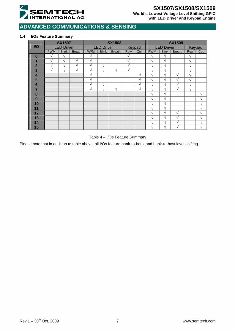
1.4 I/Os Feature Summary
SX1507 SX1508 SX1509 LED Driver LED Driver Keypad LED Driver Keypad I/O
PWM Blink Breath PWM Blink Breath Row Col. PWM Blink Breath Row Col.
0 √ √ √ √ √ √ √ 1 √ √ √ √ √ √ √ √ 2 √ √ √ √ √ √ √ √ √ 3 √ √ √ √ √ √ √ √ √ √ 4 √ √ √ √ √ √ 5 √ √ √ √ √ √ 6 √ √ √ √ √ √ √ 7 √ √ √ √ √ √ √ √ 8 √ √ √ 9 √ √ √ 10 √ √ √ 11 √ √ √ 12 √ √ √ √ 13 √ √ √ √ 14 √ √ √ √ 15 √ √ √ √
Table 4 – I/Os Feature Summary
Please note that in addition to table above, all I/Os feature bank-to-bank and bank-to-host level shifting.

ADVANCED COMMUNICATIONS & SENSING
Rev 1 – 30th Oct. 2009 8 www.semtech.com
SX1507/SX1508/SX1509 World’s Lowest Voltage Level Shifting GPIO
with LED Driver and Keypad Engine
2 ELECTRICAL CHARACTERISTICS
2.1 Absolute Maximum Ratings Table below applies to SX1508 and SX1509. Stress above the limits listed in the following table may cause permanent failure. Exposure to absolute ratings for extended time periods may affect device reliability. The limiting values are in accordance with the Absolute Maximum Rating System (IEC 134). All voltages are referenced to ground (GND).
Symbol Description Min Max Unit
Vmax_VDDM Main supply voltage - 0.4 3.7 V
Vmax_VCC1-2 Digital I/O pin supply voltage - 0.4 3.7 V
Electrostatic handling HBM model(1) (SX1508) - 2000 VES_HBM
Electrostatic handling HBM model(1) (SX1509) - 1500 V
VES_CDM Electrostatic handling CDM model - 1000 V
Electrostatic handling MM model (SX1508) - 200 VES_MM
Electrostatic handling MM model (SX1509) - 150 V
TA Operating ambient temperature range -40 +85 °C
TC Junction temperature range -40 +125 °C
TSTG Storage temperature range -55 +150 °C
Ilat Latchup-free input pin current(2) +/-100 - mA (1) Tested according to JESD22-A114A (2) Static latch-up values are valid at maximum temperature according to JEDEC 78 specification
Table 5 - Absolute Maximum Ratings
2.2 Electrical Specifications Table below applies to SX1508 and SX1509 with default registers values, unless otherwise specified. Typical values are given for TA = +25°C, VDDM=VCC1=VCC2=3.3V. Symbol Description Conditions Min Typ Max Unit Supply VDDM Main supply voltage - 1.425 - 3.6 V VCC1,2 I/O banks supply voltage - 1.2 - 3.6 V
Internal osc. OFF - 1 5 Internal osc. ON (2MHz) - 175 235
Main supply current (SX1508, I2C inactive)
External osc. (32kHz) - 10 - µA
Internal osc. OFF - 1 5 Internal osc. ON (2MHz) - 365 460
IDDM Main supply current (SX1509, I2C inactive)
External osc. (32kHz) - 10 - µA
ICC1,2 I/O banks supply current(1) - 1 2 µA I/Os set as Input
VCC1,2 >= 2V 0.7* VCC1,2 - 5.5(8)
VIH High level input voltage VCC1,2 < 2V 0.8*
VCC1,2 - 5.5(8) V
VCC1,2 >= 2V -0.4 - 0.3* VCC1,2 VIL Low level input voltage
VCC1,2 < 2V -0.4 - 0.2* VCC1,2
V
ILEAK Input leakage current Assuming no active pull-up/down -1 - 1 µA
CI Input capacitance - - - 10 pF I/Os set as Output
VOH High level output voltage - VCC1,2 – 0.3 - VCC1,2 V
VOL Low level output voltage - -0.4 - 0.3 V VCC1,2 >= 2V - - 8(2) IOH High level output source current VCC1,2 < 2V - - 2(2)
mA
IOL Low level output sink current VCC1,2 >= 2V - - 15(2) mA

ADVANCED COMMUNICATIONS & SENSING
Rev 1 – 30th Oct. 2009 9 www.semtech.com
SX1507/SX1508/SX1509 World’s Lowest Voltage Level Shifting GPIO
with LED Driver and Keypad Engine
Symbol Description Conditions Min Typ Max Unit VCC1,2 < 2V - - 8(2)
tPV Output data valid timing Cf. Figure 9 - - 200 ns NINT (Output)
VOL Low level output voltage - -0.4 - 0.3 V VDDM >= 2V - - 8 IOLM Low level output sink current VDDM < 2V - - 4
mA
tIV Interrupt valid timing From input data change - - 4 µs
tIR Interrupt reset timing From RegInterruptSource clearing - - 4 µs
NRESET (Input/Output) VOL Low level output voltage - -0.4 - 0.3 V
VDDM >= 2V - - 8 IOLM Low level output sink current VDDM < 2V - - 4
mA
VCC1,2 >= 2V 0.7* VDDM - 3.6
VIHMR High level input voltage VCC1,2 < 2V 0.8*
VDDM - 3.6 V
VCC1,2 >= 2V -0.4 - 0.3* VDDM VILM Low level input voltage
VCC1,2 < 2V -0.4 - 0.2* VDDM
V
ILEAK Input leakage current - -1 - 1 µA CI Input capacitance - - - 10 pF
VPOR Power-On-Reset voltage Cf. Figure 7 - 0.8 - V VDROPH High brown-out voltage Cf. Figure 7 - VDDM-1 - V VDROPL Low brown-out voltage Cf. Figure 7 - 0.2 - V
tRESET Reset time Cf. Figure 7 0.6 - 2.5 ms tPULSE Reset pulse from host uC Cf. Figure 7 200 - - ns
ADDR0, ADDR1 (Inputs)
VCC1,2 >= 2V 0.7* VDDM - VDDM
+0.3 VIHMA High level input voltage VCC1,2 < 2V 0.8*
VDDM - VDDM +0.3
V
VCC1,2 >= 2V -0.4 - 0.3* VDDM VILM Low level input voltage
VCC1,2 < 2V -0.4 - 0.2* VDDM
V
ILEAK Input leakage current - -1 - 1 µA CI Input capacitance - - - 10 pF
OSCIO (Input/Output)
VCC1,2 >= 2V 0.7* VDDM - VDDM
+0.3 VIHMA High level input voltage VCC1,2 < 2V 0.8*
VDDM - VDDM +0.3
V
VCC1,2 >= 2V -0.4 - 0.3* VDDM VILM Low level input voltage
VCC1,2 < 2V -0.4 - 0.2* VDDM
V
ILEAK Input leakage current - -1 - 1 µA CI Input capacitance - - - 10 pF
VOHM High level output voltage - VDDM – 0.3 - VDDM V
VOL Low level output voltage - -0.4 - 0.3 V VDDM >= 2V - - 8 IOHM High level output source current VDDM < 2V - - 2
mA
VDDM >= 2V - - 8 IOLM Low level output sink current VDDM < 2V - - 4
mA
SCL (Input) and SDA (Input/Output) (3)

ADVANCED COMMUNICATIONS & SENSING
Rev 1 – 30th Oct. 2009 10 www.semtech.com
SX1507/SX1508/SX1509 World’s Lowest Voltage Level Shifting GPIO
with LED Driver and Keypad Engine
Symbol Description Conditions Min Typ Max Unit Interface complies with slave F/S mode I2C interface as described by Philips I2C specification version 2.1 dated January, 2000. Please refer to that document for more detailed I2C specifications.
VOL Low level output voltage - -0.4 - 0.3 V
VDDM >= 2V - - 8 IOLM Low level output sink current VDDM < 2V - - 4
mA
VCC1,2 >= 2V 0.7* VDDM - 3.6
VIHMR High level input voltage VCC1,2 < 2V 0.8*
VDDM - 3.6 V
VCC1,2 >= 2V -0.4 - 0.3* VDDM VILM Low level input voltage
VCC1,2 < 2V -0.4 - 0.2* VDDM
V
fSCL SCL clock frequency - - - 400 kHz
tHD;STA Hold time (repeated) START condition - 0.6 - - µs
tLOW LOW period of the SCL clock - 1.3 - - µs tHIGH HIGH period of the SCL clock - 0.6 - - µs
tSU;STA Set-up time for a repeated START condition - 0.6 - - µs
tHD;DAT Data hold time - 0(4) - 0.9(5) µs tSU;DAT Data set-up time - 100(6) - - ns tr Rise time of both SDA and SCL - 20+0.1Cb
(7) - 300 ns tf Fall time of both SDA and SCL - 20+0.1Cb
(7) - 300 ns tSU;STO Set-up time for STOP condition - 0.6 - - µs
tBUF Bus free time between a STOP and START condition - 1.3 - - µs
Cb Capacitive load for each bus line - - - 400 pF
VnL Noise margin at the LOW level for each connected device (including hysteresis)
- - 0.1* VDDM - V
VnH Noise margin at the HIGH level for each connected device (including hysteresis)
- - 0.2* VDDM - V
tSP Pulse width of spikes suppressed by the input filter - - - 50 ns
Miscellaneous
RPULL Programmable pull-up/down resistors for IO[0-7] - - 42 - kΩ
Internal 1.3 2 2.6 fOSC Oscillator frequency External from OSCIN - - 2.6
MHz
(1) Assuming no load connected to outputs and inputs fixed to VCC1,2 or GND.
(2) Can be increased by tying together and driving simultaneously several I/Os.
(3) All values referred to VIHMR min and VILM max levels. (4) A device must internally provide a hold time of at least 300ns for the SDA signal (referred to VIHMR min) to bridge the undefined region of the falling edge of SCL. (5) The maximum tHD;DAT has only to be met if the device does not stretch the LOW period (tLOW) of the SCL signal. (6) A Fast-mode I2C-bus device can be used in a Standard-mode I2C-bus system, but the requirement tSU;DAT ≥ 250 ns must then be met. This will automatically be the case if the device does not stretch the LOW period of the SCL signal. If such a device does stretch the LOW period of the SCL signal, it must output the next data bit to the SDA line tr max+ tSU;DAT = 1000 + 250 = 1250 ns (according to the Standard-mode I2C-bus specification) before the SCL line is released. (7) Cb = total capacitance of one bus line in pF. If mixed with Hs-mode devices, faster fall-times are allowed. (8) With RegHighInput bit enabled (VCCx min =1.65V), else 3.6V (VCCx min = 1.2V)
Table 6 – Electrical Specifications

ADVANCED COMMUNICATIONS & SENSING
Rev 1 – 30th Oct. 2009 11 www.semtech.com
SX1507/SX1508/SX1509 World’s Lowest Voltage Level Shifting GPIO
with LED Driver and Keypad Engine
3 TYPICAL OPERATING CHARACTERISTICS
Figure 3 – Typical Operating Characteristics
Fosc vs.Temperature (VDDM = 3.6V)
1.3
1.5
1.7
1.9
2.1
2.3
2.5
-50 -30 -10 10 30 50 70 90
Temp (oC)
Fo
sc (
MH
z)
SX1509 IDDM vs.Temperature (VDDM = 3.6V, Oscillator Enabled)
330
335
340
345
350
355
360
365
370
-50 -30 -10 10 30 50 70 90
Temp (oC)
IDD
M (
uA
)
VOL vs.Temperature (VCCx = 3.6V, IOL = 15mA)
0
0.05
0.1
0.15
0.2
0.25
0.3
-50 -30 -10 10 30 50 70 90
Temp (oC)
VO
L (V
)
VOH vs. Temperature (VCCx = 3.6V, IOH = 8mA)
3.2
3.25
3.3
3.35
3.4
3.45
3.5
3.55
3.6
-50 -30 -10 10 30 50 70 90
Temp (oC)
VO
H (
V)
SX1509 IDDM vs.VDDM (Oscillator Enabled)
100
120
140
160
180
200
220
240
260
280
300
320
340
360
1.3 1.5 1.7 1.9 2.1 2.3 2.5 2.7 2.9 3.1 3.3 3.5
VDDM (V)
IDD
M (
uA)
VOH vs. IOH (VDDM = 3.6V, Temp 25C)
3.2
3.25
3.3
3.35
3.4
3.45
3.5
3.55
3.6
-8 -7 -6 -5 -4 -3 -2 -1 0
IOH (mA)
VO
H (
V)
VOL vs. IOL (VCCx = 3.6V, Temp 25C)
0
0.05
0.1
0.15
0.2
0.25
0.3
0 2 4 6 8 10 12 14
IOL (mA)
VO
L (V
)
Fosc vs. VDDM
1.3
1.5
1.7
1.9
2.1
2.3
2.5
1.3 1.5 1.7 1.9 2.1 2.3 2.5 2.7 2.9 3.1 3.3 3.5
VDDM (V)
Fos
c (M
Hz)

ADVANCED COMMUNICATIONS & SENSING
Rev 1 – 30th Oct. 2009 12 www.semtech.com
SX1507/SX1508/SX1509 World’s Lowest Voltage Level Shifting GPIO
with LED Driver and Keypad Engine
4 BLOCK DETAILED DESCRIPTION
4.1 SX1507 4-channel I 2C GPIO with LED Driver
Input
Filter
Reset
VDDM
I2C Bus
Control
NRESET
SCL
SDA
Interrupt
4-Bit VCC1 I/O[0] I/O[1] I/O[2] I/O[3]
R/W
GND
LED Driver
Blink (Timer)
Breath (Ramp)
Intensity (PWM)
Clock Mgmt
Internal Oscillator
I/O Bank A A
SX1507 NINT
OSCIO
External Clock
ADDR1 ADDR0
Figure 4 – 4-channel Low Voltage GPIO with LED Driver
4.2 SX1508 8-channel I 2C GPIO with LED Driver and Keypad Engine
Input
Filter
Reset
VDDM
I2C Bus
Control
VCC1
NRESET
SCL
SDA
Interrupt
8-Bit
I/O[0] I/O[1] I/O[2] I/O[3]
R/W
I/O[4] I/O[5] I/O[6] I/O[7]
ADDR1
GND
VCC2
LED Driver
Blink (Timer)
Breath (Ramp)
Intensity (PWM)
Clock Mgmt
Internal Oscillator
External Clock
I/O Bank A A
I/O Bank B A
SX1508 NINT
OSCIO
ADDR0
Keypad Engine
16 Keys Max
Figure 5 – 8-channel Low Voltage GPIO with LED Driver and Keypad Engine

ADVANCED COMMUNICATIONS & SENSING
Rev 1 – 30th Oct. 2009 13 www.semtech.com
SX1507/SX1508/SX1509 World’s Lowest Voltage Level Shifting GPIO
with LED Driver and Keypad Engine
4.3 SX1509 16-channel I 2C GPIO with LED Driver and Keypad Engine
I2C Bus
Control
VCC1
Input
Filter
Reset
VDDM
NRESET
SCL
SDA
Interrupt
8-Bit
R/W
I/O[0] I/O[1] I/O[2] I/O[3] I/O[4] I/O[5] I/O[6] I/O[7]
GND
VCC2
LED Driver
Blink (Timer)
Breath (Ramp)
Intensity (PWM)
Clock Mgmt
Internal Oscillator
External Clock
I/O Bank A A
I/O Bank B A
SX1509
I/O[8] I/O[9] I/O[10] I/O[11] I/O[12] I/O[13] I/O[14] I/O[15]
8-Bit
R/W
NINT
OSCIO
ADDR1 ADDR0
Keypad Engine
64 Keys Max Auto
Sleep/Wakeup
Figure 6 – 16-channel Low Voltage GPIO with LED Driver and Keypad Engine
4.4 Reset
4.4.1 Hardware (NRESET) The SX1507, SX1508 and SX1509 generate their own power on reset signal after a power supply is connected to the VDDM pin. The reset signal is made available for the user at the pin NRESET. The rising edge of the NRESET indicates that the startup sequence of the SX1507, SX1508 or SX1509 has finished. NRESET must be connected to VDDM (or greater) either directly, or via a resistor.
Undefined
tRESET
NRESET
VDDM
VPOR
tPULSE
VDROPH
Undefined
tRESET
Undefined
1 2 3 4 5 6 21
VDROPL
Figure 7 – Power-On / Brown-out Reset Conditions
1. Device behavior is undefined until VDDM rises above VPOR, at which point NRESET is driven to GND by the SX1507, SX1508 or SX1509.
2. After tRESET, NRESET is released (high-impedance) by the SX1507, SX1508 or SX1509 to allow it to be pulled high by an external resistor.

ADVANCED COMMUNICATIONS & SENSING
Rev 1 – 30th Oct. 2009 14 www.semtech.com
SX1507/SX1508/SX1509 World’s Lowest Voltage Level Shifting GPIO
with LED Driver and Keypad Engine
3. In operation, the SX1507, SX1508 and SX1509 may be reset (POR like or LED driver counters only depending on RegMisc setting) at anytime by an external device driving NRESET low during tPULSE. Chip can be accessed normally again after NRESET rising edge.
4. During a brown-out event, if VDDM drops above VDROPH a reset will not occur. 5. During a brown-out event, if VDDM drops between VDROPH and VDROPL a reset may occur. 6. During a brown-out event, if VDDM drops below VDROPL a reset will occur next time VPOR is crossed.
Please note that a brown-out event is defined as a transient event on VDDM. If VDDM is attached to a battery, then the gradual decay of the battery voltage will not be interpreted as a brown-out event. Please also note that a sharp rise in VDDM (> 1V/us) may induce a circuit reset.
4.4.2 Software (RegReset) Writing consecutively 0x12 and 0x34 to RegReset register will reset all registers to their default values.
4.5 2-Wire Interface (I 2C) The SX1507, SX1508 and SX1509 2-wire interface operates only in slave mode. In this configuration, the device has one or 4 possible devices addresses defined by ADDR[1:0] pins:
Device ADDR[1:0] Address Description 00 0x20 (0100000) First address of the 2-wire interface 01 0x21 (0100001) Second address of the 2-wire interface 10 0x22 (0100010) Third address of the 2-wire interface
SX1508
11 0x23 (0100011) Fourth address of the 2-wire interface 00 0x3E (0111110) First address of the 2-wire interface 01 0x3F (0111111) Second address of the 2-wire interface 10 0x70 (1110000) Third address of the 2-wire interface
SX1507 & SX1509
11 0x71 (1110001) Fourth address of the 2-wire interface Table 7 - 2-Wire Interface Address
2 lines are used to exchange data between an external master host and the slave device: • SCL : Serial CLock • SDA : Serial DAta
The SX1507, SX1508 and SX1509 are read-write slave-mode I2C devices and comply with the Philips I2C standard Version 2.1 dated January, 2000. The SX1507, SX1508 and SX1509 have a few user-accessible internal 8-bits registers to set the various parameters of operation (Cf. §5 for detailed configuration registers description). The I2C interface has been designed for program flexibility, in that once the slave address has been sent to the SX1507, SX1508 or SX1509 enabling it to be a slave transmitter/receiver, any register can be written or read independently of each other. The start and stop commands frame the data-packet and the repeat start condition is allowed if necessary. Seven bit addressing is used and ten bit addressing is not allowed. Any general call address will be ignored by the SX1507, SX1508 and SX1509. The SX1507, SX1508 and SX1509 are not CBUS compatible and can operate in standard mode (100kbit/s) or fast mode (400kbit/s).
4.5.1 WRITE
After the start condition [S], the slave address (SA) is sent, followed by an eighth bit (‘0’) indicating a Write. The slave then Acknowledges [A] that it is being addressed, and the Master sends an 8 bit Data Byte consisting of the slave Register Address (RA). The Slave Acknowledges [A] and the master sends the appropriate 8 bit Data Byte (WD0). Again the slave Acknowledges [A]. In case the master needs to write more data, a succeeding 8 bit Data Byte will follow (WD1), acknowledged by the slave [A]. This sequence will be repeated until the master terminates the transfer with the Stop condition [P].

ADVANCED COMMUNICATIONS & SENSING
Rev 1 – 30th Oct. 2009 15 www.semtech.com
SX1507/SX1508/SX1509 World’s Lowest Voltage Level Shifting GPIO
with LED Driver and Keypad Engine
Figure 8 - 2-Wire Serial Interface, Write Operation
When successive register data (WD1...WDn) is supplied by the master, the register address can be automatically incremented or kept fixed depending on the setting programmed in RegMisc.
1
Figure 9 – Example: Write RegData Register
4.5.2 READ
After the start condition [S], the slave address (SA) is sent, followed by an eighth bit (‘0’) indicating a Write. The slave then Acknowledges [A] that it is being addressed, and the Master responds with an 8 bit Data consisting of the Register Address (RA). The slave Acknowledges [A] and the master sends the Repeated Start Condition [Sr]. Once again, the slave address (SA) is sent, followed by an eighth bit (‘1’) indicating a Read.
The slave responds with an Acknowledge [A] and the read Data byte (RD0). If the master needs to read more data it will acknowledge [A] and the slave will send the next read byte (RD1). This sequence can be repeated until the master terminates with a NACK [N] followed by a stop [P].
Figure 10 - 2-Wire Serial Interface, Read Operation
When successive register data (RD1...RDn) is read by the master, the register address will be automatically incremented or kept fixed depending on the setting programmed in RegMisc.
4.6 I/O Banks
4.6.1 Input Debouncer Each input can be individually debounced by setting corresponding bits in RegDebounce register. At power up the debounce function is disabled. After enabling the debouncer, the change of the input value is accepted only if the input value is identical at two consecutive sampling times.

ADVANCED COMMUNICATIONS & SENSING
Rev 1 – 30th Oct. 2009 16 www.semtech.com
SX1507/SX1508/SX1509 World’s Lowest Voltage Level Shifting GPIO
with LED Driver and Keypad Engine
The debounce time common to all IOs can be set in RegDebounceConfig register from 0.5 to 64ms (fOSC = 2MHz).
4.6.2 Keypad Scanning Engine SX1508, and SX1509 integrate a fully programmable keypad scanning engine to implement keypad applications up to 8x8 matrix (i.e. 64 keys). Please note that SX1509 also implements an Auto Sleep/Wakeup feature to save power consumption when no key has been pressed for a programmed time.
IO3
IO2
IO1
IO0
IO4
IO5
IO6
IO7
SX1508
- IO[3-0] as outputs (scanning) - IO[7-4] as inputs
X
Y
RegKeyData =
X Y Figure 11 – 4x4 Keypad Connection to SX1508
Following procedure should be implemented on the host controller for a 4x4 keypad: 1. Set RegDir to 0xF0 (IO[3-0] as outputs, IO[7-4] as inputs) , set RegOpenDrain to 0x0F (IO[3-0] as open-drain outputs), set RegPullup to 0xF0 (pull-ups enabled on inputs IO[7-4]). 2. Enable and configure debouncing on IO[7-4] (RegDebounceEnable = 0xF0, Ex : RegDebounceConfig = 0x05) 3. Enable and configure keypad scanning engine (Ex : RegKeyConfig = 0x7D) This will start an infinite loop with the following sequence to IO[3:0]: ZZZ0, ZZ0Z, Z0ZZ, 0ZZZ. Make sure that scan interval is set to higher value than the debounce time.
4. When a key is pressed, NINT goes low, key scan is halted and the key coordinates are stored in RegKeyData:
• The column data will be stored in RegKeyData[7:4] (Note: column indication is active low)
• The row data will be stored in RegKeyData[3:0] (Note: row indication is active low)
• When RegKeyData is read, this data along with the interrupt is automatically cleared (same behavior as reading RegData) and the key scan continues to the next row.
5. Restart from point 4.
This implementation allows the host to handle both single and multi-touches easily (fast AAAAAA sequence is a long press of key A, fast ABABABAB sequence is key A and key B pressed together, etc)
4.6.3 Level Shifter Because of their 5.5V tolerant I/O banks with independent supply voltages between 1.2V and 3.6V, the SX1508 and SX1509 can perform level shifting of signals from one I/O bank to another without uC activity by programming the corresponding configuration register bits accordingly in RegLevelShifter (and RegDir). This can save significant BOM cost in a final application where only a few signals need to be level-shifted (no need for an additional external level shifter IC).

ADVANCED COMMUNICATIONS & SENSING
Rev 1 – 30th Oct. 2009 17 www.semtech.com
SX1507/SX1508/SX1509 World’s Lowest Voltage Level Shifting GPIO
with LED Driver and Keypad Engine
VCC1
IO0
1.2-3.6V
SX1508/9
VCC2
IO4
1.2-3.6V
1.2-5.5V
1.2-3.6V
tLevelShiftMin
Figure 12 – Level Shifting Example
The minimum pulse width tLevelShiftMin which can be level shifted properly depends on VCCx and VDDM:
tLevelShiftMin = Input Delay + Core Delay + Output Delay Input/Core/Output delays vs VCCx/VDDM are given in figures below.
Figure 13 – Level Shifter Max Frequency Calculation Data
SX1509 Digital Core Delay vs. Supply Voltage
14
16
18
20
22
24
26
28
1 1.5 2 2.5 3 3.5
VDDM (V)
Tde
lay
(ns)
Typical Worst Case
IO Input Delay vs. Supply Voltage
0.000
1.000
2.000
3.000
4.000
5.000
6.000
7.000
8.000
9.000
10.000
1.000 1.500 2.000 2.500 3.000 3.500
VCCx (V)
Tde
lay
(ns)
Typical Worst Case
SX1508 Digital Core Delay vs. Supply Voltage
14
16
18
20
22
24
26
28
1 1.5 2 2.5 3 3.5
VDDM (V)
Tdel
ay
(ns)
Typical Worst Case
IO Output Delay vs. Supply Voltage ( LowDriveEn=0, 20pF Load)
0.000
20.000
40.000
60.000
80.000
100.000
120.000
140.000
1.000 1.500 2.000 2.500 3.000 3.500
VCCx (V)
Tde
lay
(ns)
Typical Worst Case
IO Output Delay vs. Supply Voltage (LowDriveEn=1, 20pF Load)
0.000
20.000
40.000
60.000
80.000
100.000
120.000
140.000
1.000 1.500 2.000 2.500 3.000 3.500
VCCx (V)
Tdel
ay
(ns)
Typical Worst Case

ADVANCED COMMUNICATIONS & SENSING
Rev 1 – 30th Oct. 2009 18 www.semtech.com
SX1507/SX1508/SX1509 World’s Lowest Voltage Level Shifting GPIO
with LED Driver and Keypad Engine
4.6.4 Polarity Inverter Each IO’s polarity can be individually inverted by setting corresponding bit in RegPolarity register. Please note that polarity inversion can also be combined with level shifting feature.
4.7 Interrupt (NINT) At start-up, the transition detection logic is reset, and NINT is released to a high-impedance state. The interrupt mask register is set to 0xFF, disabling the interrupt output for transitions on all I/O ports. The transition flags are cleared to indicate no data changes. An interrupt NINT can be generated on any programmed combination of I/Os rising and/or falling edges through the RegInterruptMask and RegSense registers. If needed, the I/Os which triggered the interrupt can then be identified by reading RegInterruptSource register. When NINT is low (i.e. interrupt occurred), it can be reset back high (i.e. cleared) by writing 0xFF in RegInterruptSource (this will also clear corresponding bits in RegEventStatus register). The interrupt can also be cleared automatically when reading RegData register (Cf. RegMisc) Example: We want to detect rising edge of I/O[1] on SX1508 (NINT will go low).
1. We enable interrupt on I/O[1] in RegInterruptMask RegInterruptMask =“XXXXXX0X” 2. We set edge sense for I/O[1] in RegSense RegSenseLow =“XXXX01XX”
Please note that independently from the “user defined” process described above the keypad engine, when enabled, also uses NINT to indicate a key press. Hence we have NINT = “user defined condition occurred” OR “keypad engine condition occurred”.
4.8 Clock Management A main oscillator clock fOSC is needed by the LED driver, keypad engine and debounce features. Clock management block is illustrated in figure below.
OSCIO
Clock Mgmt
Internal Oscillator
External Clock fOSC Div
Figure 14 – Clock Management Overview
The block is configured in register RegClock (Cf §5 for more detailed information): Selection of internal clock source: none (OFF) or internal oscillator or external clock input from OSCIN. Definition of OSCIO pin function (OSCIN or OSCOUT) OSCOUT frequency setting (sub-multiple of fOSC)
Please note that if needed the OSCOUT feature can be used as an additional GPO (Cf. RegClock)
4.9 LED Driver
4.9.1 Overview Every IO has its own independent LED driver to perform intensity control, blinking and fading operation. (Cf §6.2 for typical LED connection) Please note that while all I/Os can perform intensity control (PWM) only some of them additionally include blinking and breathing features (Cf pin description §1) The LED drivers of all I/Os share the same clock ClkX configurable in RegMisc[6:4]. Please note that for power consumption reasons ClkX is OFF by default.

ADVANCED COMMUNICATIONS & SENSING
Rev 1 – 30th Oct. 2009 19 www.semtech.com
SX1507/SX1508/SX1509 World’s Lowest Voltage Level Shifting GPIO
with LED Driver and Keypad Engine
Assuming ClkX is not OFF, LED driver for IO[X] is enabled when RegLEDDriverEnable[X] = 1 in which case it can operate in one of the three modes below:
• Static mode (all I/Os, with or without fade in/out)
• Single shot mode (blinking capable I/Os only, with or without fade in/out)
• Blink mode (blinking capable I/Os only, with or without fade in/out)
t
t
1
0
Fade In
ON
Fade Out
OFF
0
100%
TRiseX TFallX TOnX TOffX
IO[X] Intensity (PWM value)
RegData[X]
IOffX
IOnX
Figure 15 – LED Driver Overview
Each IO[X] has its own set of programmable registers (Cf §5 for more detailed information):
RegTOnX (blinking capable I/Os only): TOnX, ON time of IO[X] RegIOnX (all I/Os): IOnX, ON intensity of IO[X] RegOffX (blinking capable I/Os only): TOffX and IOffX, OFF time and intensity of IO[X] RegTRiseX (breathing capable I/Os only): TRiseX, fade in time of IO[X] RegTFallX (breathing capable I/Os only): TFallX, fade out time of IO[X]
Please note that the LED driver mode is selectable for each IO bank between linear and logarithmic. (Cf §4.9.5) All the figures assume normal IO polarity, for inverse polarity RegData control must be inverted (does not invert the polarity of the IO signal itself).
4.9.2 Static Mode Only mode available for non blinking capable IOs (with Off intensity = 0), else invoked when TOnX = 0. If the I/O doesn’t support fading the LED intensity will step directly to the IOnX/IOffX value.
RegData(X)
IOLED(X) level
Off intensity(min) determined byregister RegIOffX
On intensity(max) determined by register RegIOnX
Fade in rate determined byregister RegTRiseX
Fade out rate determinedby register RegTFallX
Figure 16 – LED Driver Static Mode

ADVANCED COMMUNICATIONS & SENSING
Rev 1 – 30th Oct. 2009 20 www.semtech.com
SX1507/SX1508/SX1509 World’s Lowest Voltage Level Shifting GPIO
with LED Driver and Keypad Engine
4.9.3 Single Shot Mode Invoked when TOnX != 0 and TOffX = 0. If the I/O doesn’t support fading the LED intensity will step directly to the IOnX/IOffX value.
IOLED(X) levelOn intensity(max)
Off intensity(min)
RegData(X)
Fade in rate determined byregister RegTRiseX
Minimum intensity durationdetermined by register
RegData(x)
Fade out rate determinedby register RegTFallX
Figure 17 – LED Driver Single Shot Mode
4.9.4 Blink Mode Invoked when TOnX != 0 and TOffX != 0. If the I/O doesn’t support fading the LED intensity will step directly to the IOnX/IOffX value.
Off intensity(min)
RegData(X)
IOLED(X) level
Fade in rate determined byregister RegTRiseX Minimum intensity duration
determined by registerRegTOffX
Maximum intensityduration determined by
register RegTOnX
Fade out rate determinedby register RegTFallX
When RegData(X) is cleared, the LEDwill complete any current ramp, and then
stay at minimum intensity
On intensity(max)
Figure 18 – LED Driver Blink Mode
4.9.5 LED Driver Modes For each IO bank, the LED driver mode of fading capable IOs can be selected between linear or logarithmic in RegMisc. Lin. Log. Lin. Log. Lin. Log. Lin. Log. Lin. Log. Lin. Log. Lin. Log. Lin. Log.
0 0 32 4 64 13 96 28 128 53 160 88 192 135 224 198 1 0 33 4 65 13 97 28 129 53 161 88 193 135 225 198 2 0 34 4 66 13 98 30 130 53 162 88 194 135 226 198 3 0 35 4 67 13 99 30 131 53 163 88 195 135 227 198 4 0 36 5 68 14 100 31 132 56 164 93 196 142 228 207 5 0 37 5 69 14 101 31 133 56 165 93 197 142 229 207 6 0 38 5 70 14 102 32 134 56 166 93 198 142 230 207 7 0 39 5 71 14 103 32 135 56 167 93 199 142 231 207

ADVANCED COMMUNICATIONS & SENSING
Rev 1 – 30th Oct. 2009 21 www.semtech.com
SX1507/SX1508/SX1509 World’s Lowest Voltage Level Shifting GPIO
with LED Driver and Keypad Engine
8 1 40 6 72 16 104 34 136 60 168 98 200 150 232 216 9 1 41 6 73 16 105 34 137 60 169 98 201 150 233 216 10 1 42 6 74 17 106 35 138 60 170 98 202 150 234 216 11 1 43 6 75 17 107 35 139 60 171 98 203 150 235 216 12 1 44 7 76 18 108 36 140 65 172 104 204 157 236 225 13 1 45 7 77 18 109 36 141 65 173 104 205 157 237 225 14 1 46 7 78 19 110 38 142 65 174 104 206 157 238 225 15 1 47 7 79 19 111 38 143 65 175 104 207 157 239 225 16 2 48 8 80 20 112 39 144 69 176 110 208 165 240 235 17 2 49 8 81 20 113 39 145 69 177 110 209 165 241 235 18 2 50 8 82 21 114 41 146 69 178 110 210 165 242 235 19 2 51 8 83 21 115 41 147 69 179 110 211 165 243 235 20 2 52 9 84 22 116 42 148 73 180 116 212 172 244 245 21 2 53 9 85 22 117 42 149 73 181 116 213 172 245 245 22 2 54 9 86 23 118 44 150 73 182 116 214 172 246 245 23 2 55 9 87 23 119 44 151 73 183 116 215 172 247 245 24 3 56 10 88 24 120 46 152 78 184 122 216 181 248 255 25 3 57 10 89 24 121 46 153 78 185 122 217 181 249 255 26 3 58 10 90 25 122 46 154 78 186 122 218 181 250 255 27 3 59 10 91 25 123 46 155 78 187 122 219 181 251 255 28 3 60 11 92 26 124 49 156 83 188 129 220 189 252 255 29 3 61 11 93 26 125 49 157 83 189 129 221 189 253 255 30 3 62 12 94 27 126 49 158 83 190 129 222 189 254 255 31 3 63 12 95 27 127 49 159 83 191 129 223 189 255 255
Table 8 – LED Driver Linear vs Logarithmic Function (I)
0
50
100
150
200
250
300
1 10 19 28 37 46 55 64 73 82 91 100 109 118 127 136 145 154 163 172 181 190 199 208 217 226 235 244 253
RegIOn (4xRegOff[2:0])
IO
n (I
Off)
Linear mode
Log mode
Figure 19 – LED Driver Linear vs Logarithmic Function (II)
4.9.6 Synchronization of LED Drivers across several ICs When several GPIO expanders are used in the same application it may be useful that their LEDs drivers are synchronous for coherent global operation. In this case all ICs should share their fOSC through their OSCIO pins and have their NRESET pins connected together. When RegMisc of each IC is set accordingly, NRESET signal can then be used to reset all devices’ internal counters (but not the register settings) and allow synchronous LED operation (blinking, fading) across multiple devices.

ADVANCED COMMUNICATIONS & SENSING
Rev 1 – 30th Oct. 2009 22 www.semtech.com
SX1507/SX1508/SX1509 World’s Lowest Voltage Level Shifting GPIO
with LED Driver and Keypad Engine
4.9.7 Tutorial Below are the steps required to use the LED driver with the typical LED connection described §6.2:
- Disable input buffer (RegInputDisable) - Disable pull-up (RegPullUp) - Enable open drain (RegOpenDrain) - Set direction to output (RegDir) – by default RegData is set high => LED OFF - Enable oscillator (RegClock) - Configure LED driver clock and mode if relevant (RegMisc) - Enable LED driver operation (RegLEDDriverEnable) - Configure LED driver parameters (RegTOn, RegIOn, RegOff, RegTRise, RegTFall) - Set RegData bit low => LED driver started

ADVANCED COMMUNICATIONS & SENSING
Rev 1 – 30th Oct. 2009 23 www.semtech.com
SX1507/SX1508/SX1509 World’s Lowest Voltage Level Shifting GPIO
with LED Driver and Keypad Engine
5 CONFIGURATION REGISTERS
5.1 SX1507 4-channel GPIO with LED Driver
Address Name Description Default Device and IO Banks
0x00 RegInputDisable Input buffer disable register XXXX 0000 0x01 RegLongSlew Output buffer long slew register XXXX 0000 0x02 RegLowDrive Output buffer low drive register XXXX 0000 0x03 RegPullUp Pull-up register XXXX 0000 0x04 RegPullDown Pull-down register XXXX 0000 0x05 RegOpenDrain Open drain register XXXX 0000
0x06 RegPolarity Polarity register XXXX 0000 0x07 RegDir Direction register XXXX 1111 0x08 RegData Data register XXXX 1111* 0x09 RegInterruptMask Interrupt mask register XXXX 1111 0x0A RegSense Sense register 0000 0000 0x0B RegInterruptSource Interrupt source register XXXX 0000 0x0C RegEventStatus Event status register XXXX 0000 0x0D RegClock Clock management register 0000 0000 0x0E RegMisc Miscellaneous device settings register 0000 0000 0x0F RegLEDDriverEnable LED driver enable register XXXX 0000
Debounce 0x10 RegDebounceConfig Debounce configuration register 0000 0000 0x11 RegDebounceEnable Debounce enable register XXXX 0000
LED Driver (PWM, blinking, breathing) 0x12 RegTOn0 ON time register for I/O[0] 0000 0000 0x13 RegIOn0 ON intensity register for I/O[0] 1111 1111 0x14 RegOff0 OFF time/intensity register for I/O[0] 0000 0000 0x15 RegTOn1 ON time register for I/O[1] 0000 0000 0x16 RegIOn1 ON intensity register for I/O[1] 1111 1111 0x17 RegOff1 OFF time/intensity register for I/O[1] 0000 0000 0x18 RegTRise1 Fade in register for I/O[1] 0000 0000 0x19 RegTFall1 Fade out register for I/O[1] 0000 0000 0x1A RegTOn2 ON time register for I/O[2] 0000 0000 0x1B RegIOn2 ON intensity register for I/O[2] 1111 1111 0x1C RegOff2 OFF time/intensity register for I/O[2] 0000 0000 0x1D RegTRise2 Fade in register for I/O[2] 0000 0000 0x1E RegTFall2 Fade out register for I/O[2] 0000 0000 0x1F RegTOn3 ON time register for I/O[3] 0000 0000 0x20 RegIOn3 ON intensity register for I/O[3] 1111 1111 0x21 RegOff3 OFF time/intensity register for I/O[3] 0000 0000 0x22 RegTRise3 Fade in register for I/O[3] 0000 0000 0x23 RegTFall3 Fade out register for I/O[3] 0000 0000
Software Reset 0x7D RegReset Software reset register 0000 0000
Test (not to be written) 0x7E RegTest1 Test register 0000 0000 0x7F RegTest2 Test register 0000 0000
*Bits set as output take “1” as default value. Table 9 – SX1507 Configuration Registers Overview

ADVANCED COMMUNICATIONS & SENSING
Rev 1 – 30th Oct. 2009 24 www.semtech.com
SX1507/SX1508/SX1509 World’s Lowest Voltage Level Shifting GPIO
with LED Driver and Keypad Engine
Addr Name Default Bits Description
7:4 Unused
0x00 RegInputDisable 0xX0 3:0
Disables the input buffer of each IO 0 : Input buffer is enabled (input actually being used) 1 : Input buffer is disabled (input actually not being used or LED connection)
7:4 Unused
0x01 RegLongSlew 0xX0 3:0
Enables increased slew rate of the output buffer of each [output-configured] IO 0 : Increased slew rate is disabled 1 : Increased slew rate is enabled
7:4 Unused
0x02 RegLowDrive 0xX0 3:0
Enables reduced drive of the output buffer of each [output-configured] IO 0 : Reduced drive is disabled 1 : Reduced drive is enabled
7:4 Unused
0x03 RegPullUp 0xX0 3:0
Enables the pull-up for each IO 0 : Pull-up is disabled 1 : Pull-up is enabled
7:4 Unused
0x04 RegPullDown 0xX0 3:0
Enables the pull-down for each IO 0 : Pull-down is disabled 1 : Pull-down is enabled
7:4 Unused
0x05 RegOpenDrain 0xX0 3:0
Enables open drain operation for each [output-configured] IO 0 : Regular push-pull operation 1 : Open drain operation
7:4 Unused
0x06 RegPolarity 0xX0 3:0
Enables polarity inversion for each IO 0 : Normal polarity : RegData[x] = IO[x] 1 : Inverted polarity : RegData[x] = !IO[x] (for both input and output configured IOs)
7:4 Unused
0x07 RegDir 0xXF 3:0
Configures direction for each IO. 0 : IO is configured as an output 1 : IO is configured as an input
7:4 Unused 0x08 RegData 0xXF
3:0 Write: Data to be output to the output-configured IOs Read: Data seen at the IOs, independent of the direction configured.
7:4 Unused
0x09 RegInterruptMask 0xXF 3:0
Configures which [input-configured] IO will trigger an interrupt on NINT pin 0 : An event on this IO will trigger an interrupt 1 : An event on this IO will NOT trigger an interrupt
7:6 Edge sensitivity of RegData[3] 5:4 Edge sensitivity of RegData[2] 3:2 Edge sensitivity of RegData[1]
0x0A RegSense 0x00
1:0 Edge sensitivity of RegData[0]
00 : None 01 : Rising 10 : Falling 11 : Both
7:4 Unused
0x0B RegInterruptSource 0xX0 3:0
Interrupt source (from IOs set in RegInterruptMask) 0 : No interrupt has been triggered by this IO 1 : An interrupt has been triggered by this IO (an event as configured in relevant RegSense register occured). Writing '1' clears the bit in RegInterruptSource and in RegEventStatus When all bits are cleared, NINT signal goes back high.
7:4 Unused
0x0C RegEventStatus 0xX0 3:0
Event status of all IOs. 0 : No event has occured on this IO 1 : An event has occured on this IO (an edge as configured in relevant RegSense register occured). Writing '1' clears the bit in RegEventStatus and in RegInterruptSource if relevant. If the edge sensitivity of the IO is changed, the bit(s) will be cleared automatically
7 Unused
6:5
Oscillator frequency (fOSC) source 00 : OFF. LED driver and debounce features are disabled. 01 : External clock input (OSCIN) 10 : Internal 1MHz oscillator 11 : Reserved
4 OSCIO pin function (Cf. §4.8) 0 : OSCIO is an input (OSCIN) 1 : OSCIO is an output (OSCOUT)
0x0D RegClock 0x00
3:0
Frequency of the signal output on OSCOUT pin: 0x0 : 0Hz, permanent "0" logical level (GPO) 0xF : 0Hz, permanent "1" logical level (GPO) Else : fOSCOUT = fOSC/(2^(RegClock[3:0]-1))

ADVANCED COMMUNICATIONS & SENSING
Rev 1 – 30th Oct. 2009 25 www.semtech.com
SX1507/SX1508/SX1509 World’s Lowest Voltage Level Shifting GPIO
with LED Driver and Keypad Engine
7 Unused
6:4 Frequency of the LED Driver clock ClkX of all IOs: 0 : OFF. LED driver functionality is disabled for all IOs. Else : ClkX = fOSC/(2^(RegMisc[6:4]-1))
3 LED Driver mode for Bank A ‘s fading capable IOs (IO1-3) 0: Linear 1: Logarithmic
2
NRESET pin function when externally forced low (Cf. §4.4.1 and §4.9.5). 0: Equivalent to POR 1: Reset PWM/Blink/Fade counters (not user programmed values) This bit is can only be reset manually or by POR, not by NRESET.
1 Auto-increment register address (Cf. §4.5) 0: ON. When several consecutive data are read/written, register address is incremented. 1: OFF. When several consecutive data are read/written, register address is kept fixed.
0x0E RegMisc 0x00
0
Autoclear NINT on RegData read (Cf. §4.7) 0: ON. RegInterruptSource is also automatically cleared when RegData is read. 1: OFF. RegInterruptSource must be manually cleared, either directly or via RegEventStatus.
7:4 Unused
0x0F RegLEDDriverEnable 0xX0 3:0
Enables LED Driver for each [output-configured] IO 0 : LED Driver is disabled 1 : LED Driver is enabled
7:3 Unused
0x10 RegDebounceConfig 0x00 2:0
Debounce time (Cf. §4.6.1) 000: 0.5ms x 1MHz/fOSC 001: 1ms x 1MHz/fOSC 010: 2ms x 1MHz/fOSC 011: 4ms x 1MHz/fOSC 100: 8ms x 1MHz/fOSC 101: 16ms x 1MHz/fOSC 110: 32ms x 1MHz/fOSC 111: 64ms x 1MHz/fOSC
7:4 Unused
0x11 RegDebounceEnable 0xX0 3:0
Enables debouncing for each [input-configured] IO 0 : Debouncing is disabled 1 : Debouncing is enabled
7:5 Unused
0xXX RegTOnX 0x00 4:0
ON Time of IO[X]: 0 : Infinite (Static mode, TOn directly controlled by RegData, Cf §4.9.2) 1 - 15 : TOnX = 64 * RegTOnX * (255/ClkX) 16 - 31 : TOnX = 512 * RegTOnX * (255/ClkX)
0xXX RegIOnX 0xFF 7:0 ON Intensity of IO[X] - Linear mode : IOnX = RegIOnX - Logarithmic mode (fading capable IOs only) : IOnX = f(RegIOnX) , Cf §4.9.5
7:3
OFF Time of IO[X]: 0 : Infinite (Single shot mode, TOff directly controlled by RegData, Cf §4.9.3) 1 - 15 : TOffX = 64 * RegOffX[7:3] * (255/ClkX) 16 - 31 : TOffX = 512 * RegOffX[7:3] * (255/ClkX) 0xXX RegOffX 0x00
2:0 OFF Intensity of IO[X] - Linear mode : IOffX = 4 x RegOff[2:0] - Logarithmic mode (fading capable IOs only) : IOffX = f(4 x RegOffX[2:0]) , Cf §4.9.5
7:5 Unused
0xXX RegTRiseX 0x00 4:0
Fade In setting of IO[X] 0 : OFF 1 - 15 : TRiseX = (RegIOnX-(4xRegOffX[2:0])) * RegTRiseX * (255/ClkX) 16 - 31 : TRiseX = 16 * (RegIOnX-(4xRegOffX[2:0])) * RegTRiseX * (255/ClkX)
7:5 Unused
0xXX RegTFallX 0x00 4:0
Fade Out setting of IO[X] 0 : OFF 1 - 15 : TFallX = (RegIOnX-(4xRegOffX[2:0])) * RegTFallX * (255/ClkX) 16 - 31 : TFallX = 16 * (RegIOnX-(4xRegOffX[2:0])) * RegTFallX * (255/ClkX)
0x7D RegReset 0x00 7:0 Software reset register Writing consecutively 0x12 and 0x34 will reset the device (same as POR). Always reads 0.
Table 10 – SX1507 Configuration Registers Description

ADVANCED COMMUNICATIONS & SENSING
Rev 1 – 30th Oct. 2009 26 www.semtech.com
SX1507/SX1508/SX1509 World’s Lowest Voltage Level Shifting GPIO
with LED Driver and Keypad Engine
5.2 SX1508 8-channel GPIO with LED Driver and Keypa d Engine
Address Name Description Default Device and IO Banks
0x00 RegInputDisable Input buffer disable register 0000 0000 0x01 RegLongSlew Output buffer long slew register 0000 0000 0x02 RegLowDrive Output buffer low drive register 0000 0000 0x03 RegPullUp Pull-up register 0000 0000 0x04 RegPullDown Pull-down register 0000 0000 0x05 RegOpenDrain Open drain register 0000 0000
0x06 RegPolarity Polarity register 0000 0000 0x07 RegDir Direction register 1111 1111 0x08 RegData Data register 1111 1111* 0x09 RegInterruptMask Interrupt mask register 1111 1111 0x0A RegSenseHigh Sense register for I/O[7:4] 0000 0000 0x0B RegSenseLow Sense register for I/O[3:0] 0000 0000 0x0C RegInterruptSource Interrupt source register 0000 0000 0x0D RegEventStatus Event status register 0000 0000 0x0E RegLevelShifter Level shifter register 0000 0000 0x0F RegClock Clock management register 0000 0000 0x10 RegMisc Miscellaneous device settings register 0000 0000 0x11 RegLEDDriverEnable LED driver enable register 0000 0000
Debounce and Keypad Engine 0x12 RegDebounceConfig Debounce configuration register 0000 0000 0x13 RegDebounceEnable Debounce enable register 0000 0000 0x14 RegKeyConfig Key scan configuration register 0000 0000 0x15 RegKeyData Key value 1111 1111
LED Driver (PWM, blinking, breathing) 0x16 RegIOn0 ON intensity register for I/O[0] 1111 1111 0x17 RegIOn1 ON intensity register for I/O[1] 1111 1111 0x18 RegTOn2 ON time register for I/O[2] 0000 0000 0x19 RegIOn2 ON intensity register for I/O[2] 1111 1111 0x1A RegOff2 OFF time/intensity register for I/O[2] 0000 0000 0x1B RegTOn3 ON time register for I/O[3] 0000 0000 0x1C RegIOn3 ON intensity register for I/O[3] 1111 1111 0x1D RegOff3 OFF time/intensity register for I/O[3] 0000 0000 0x1E RegTRise3 Fade in register for I/O[3] 0000 0000 0x1F RegTFall3 Fade out register for I/O[3] 0000 0000 0x20 RegIOn4 ON intensity register for I/O[4] 1111 1111 0x21 RegIOn5 ON intensity register for I/O[5] 1111 1111 0x22 RegTOn6 ON time register for I/O[6] 0000 0000 0x23 RegIOn6 ON intensity register for I/O[6] 1111 1111 0x24 RegOff6 OFF time/intensity register for I/O[6] 0000 0000 0x25 RegTOn7 ON time register for I/O[7] 0000 0000 0x26 RegIOn7 ON intensity register for I/O[7] 1111 1111 0x27 RegOff7 OFF time/intensity register for I/O[7] 0000 0000 0x28 RegTRise7 Fade in register for I/O[7] 0000 0000 0x29 RegTFall7 Fade out register for I/O[7] 0000 0000
Miscellaneous 0x2A RegHighInput High input enable register 0000 0000
Software Reset 0x7D RegReset Software reset register 0000 0000
Test (not to be written) 0x7E RegTest1 Test register 0000 0000 0x7F RegTest2 Test register 0000 0000
*Bits set as output take “1” as default value. Table 11 – SX1508 Configuration Registers Overview

ADVANCED COMMUNICATIONS & SENSING
Rev 1 – 30th Oct. 2009 27 www.semtech.com
SX1507/SX1508/SX1509 World’s Lowest Voltage Level Shifting GPIO
with LED Driver and Keypad Engine
Addr Name Default Bits Description
0x00 RegInputDisable 0x00 7:0 Disables the input buffer of each IO 0 : Input buffer is enabled (input actually being used) 1 : Input buffer is disabled (input actually not being used or LED connection)
0x01 RegLongSlew 0x00 7:0 Enables increased slew rate of the output buffer of each [output-configured] IO 0 : Increased slew rate is disabled 1 : Increased slew rate is enabled
0x02 RegLowDrive 0x00 7:0 Enables reduced drive of the output buffer of each [output-configured] IO 0 : Reduced drive is disabled 1 : Reduced drive is enabled
0x03 RegPullUp 0x00 7:0 Enables the pull-up for each IO 0 : Pull-up is disabled 1 : Pull-up is enabled
0x04 RegPullDown 0x00 7:0 Enables the pull-down for each IO 0 : Pull-down is disabled 1 : Pull-down is enabled
0x05 RegOpenDrain 0x00 7:0 Enables open drain operation for each [output-configured] IO 0 : Regular push-pull operation 1 : Open drain operation
0x06 RegPolarity 0x00 7:0 Enables polarity inversion for each IO 0 : Normal polarity : RegData[x] = IO[x] 1 : Inverted polarity : RegData[x] = !IO[x] (for both input and output configured IOs)
0x07 RegDir 0xFF 7:0 Configures direction for each IO. 0 : IO is configured as an output 1 : IO is configured as an input
0x08 RegData 0xFF 7:0 Write: Data to be output to the output-configured IOs Read: Data seen at the IOs, independent of the direction configured.
0x09 RegInterruptMask 0xFF 7:0 Configures which [input-configured] IO will trigger an interrupt on NINT pin 0 : An event on this IO will trigger an interrupt 1 : An event on this IO will NOT trigger an interrupt
7:6 Edge sensitivity of RegData[7] 5:4 Edge sensitivity of RegData[6] 3:2 Edge sensitivity of RegData[5]
0x0A RegSenseHigh 0x00
1:0 Edge sensitivity of RegData[4]
00 : None 01 : Rising 10 : Falling 11 : Both
7:6 Edge sensitivity of RegData[3] 5:4 Edge sensitivity of RegData[2] 3:2 Edge sensitivity of RegData[1]
0x0B RegSenseLow 0x00
1:0 Edge sensitivity of RegData[0]
00 : None 01 : Rising 10 : Falling 11 : Both
0x0C RegInterruptSource 0x00 7:0
Interrupt source (from IOs set in RegInterruptMask) 0 : No interrupt has been triggered by this IO 1 : An interrupt has been triggered by this IO (an event as configured in relevant RegSense register occured). Writing '1' clears the bit in RegInterruptSource and in RegEventStatus When all bits are cleared, NINT signal goes back high.
0x0D RegEventStatus 0x00 7:0
Event status of all IOs. 0 : No event has occured on this IO 1 : An event has occured on this IO (an edge as configured in relevant RegSense register occured). Writing '1' clears the bit in RegEventStatus and in RegInterruptSource if relevant. If the edge sensitivity of the IO is changed, the bit(s) will be cleared automatically
7:6 Level shifter mode for IO[3] (Bank A) and IO[7] (Bank B) 5:4 Level shifter mode for IO[2] (Bank A) and IO[6] (Bank B) 3:2 Level shifter mode for IO[1] (Bank A) and IO[5] (Bank B)
0x0E RegLevelShifter 0x00
1:0 Level shifter mode for IO[0] (Bank A) and IO[4] (Bank B)
00 : OFF 01 : A->B 10 : B->A 11 : Reserved
7 Unused
6:5
Oscillator frequency (fOSC) source 00 : OFF. LED driver, keypad engine and debounce features are disabled. 01 : External clock input (OSCIN) 10 : Internal 2MHz oscillator 11 : Reserved
4 OSCIO pin function (Cf. §4.8) 0 : OSCIO is an input (OSCIN) 1 : OSCIO is an output (OSCOUT)
0x0F RegClock 0x00
3:0
Frequency of the signal output on OSCOUT pin: 0x0 : 0Hz, permanent "0" logical level (GPO) 0xF : 0Hz, permanent "1" logical level (GPO) Else : fOSCOUT = fOSC/(2^(RegClock[3:0]-1))
0x10 RegMisc 0x00 7 LED Driver mode for Bank B ‘s fading capable IOs (IO7) 0: Linear 1: Logarithmic

ADVANCED COMMUNICATIONS & SENSING
Rev 1 – 30th Oct. 2009 28 www.semtech.com
SX1507/SX1508/SX1509 World’s Lowest Voltage Level Shifting GPIO
with LED Driver and Keypad Engine
6:4 Frequency of the LED Driver clock ClkX of all IOs: 0 : OFF. LED driver functionality is disabled for all IOs. Else : ClkX = fOSC/(2^(RegMisc[6:4]-1))
3 LED Driver mode for Bank A ‘s fading capable IOs (IO3) 0: Linear 1: Logarithmic
2
NRESET pin function when externally forced low (Cf. §4.4.1 and §4.9.5). 0: Equivalent to POR 1: Reset PWM/Blink/Fade counters (not user programmed values) This bit is can only be reset manually or by POR, not by NRESET.
1 Auto-increment register address (Cf. §4.5) 0: ON. When several consecutive data are read/written, register address is incremented. 1: OFF. When several consecutive data are read/written, register address is kept fixed.
0
Autoclear NINT on RegData read (Cf. §4.7) 0: ON. RegInterruptSource is also automatically cleared when RegData is read. 1: OFF. RegInterruptSource must be manually cleared, either directly or via RegEventStatus.
0x11 RegLEDDriverEnable 0x00 7:0 Enables LED Driver for each [output-configured] IO 0 : LED Driver is disabled 1 : LED Driver is enabled
7:3 Unused
0x12 RegDebounceConfig 0x00 2:0
Debounce time (Cf. §4.6.1) 000: 0.5ms x 2MHz/fOSC 001: 1ms x 2MHz/fOSC 010: 2ms x 2MHz/fOSC 011: 4ms x 2MHz/fOSC 100: 8ms x 2MHz/fOSC 101: 16ms x 2MHz/fOSC 110: 32ms x 2MHz/fOSC 111: 64ms x 2MHz/fOSC
0x13 RegDebounceEnable 0x00 7:0 Enables debouncing for each [input-configured] IO 0 : Debouncing is disabled 1 : Debouncing is enabled
7 Unused
6:5
Number of rows (outputs) + key scan enable 00 : Key scan OFF 01 : 2 rows – IO[0:1] 10 : 3 rows – IO[0:2] 11 : 4 rows – IO[0:3]
4:3
Number of columns (inputs) 00 : 1 column – IO[4] 01 : 2 columns – IO[4:5] 10 : 3 columns – IO[4:6] 11 : 4 columns – IO[4:7]
0x14 RegKeyConfig 0x00
2:0
Scan time per row (must be set above debounce time). 000 : 1ms x 2MHz/fOSC 001 : 2ms x 2MHz/fOSC 010 : 4ms x 2MHz/fOSC 011 : 8ms x 2MHz/fOSC 100 : 16ms x 2MHz/fOSC 101 : 32ms x 2MHz/fOSC 110 : 64ms x 2MHz/fOSC 111 : 128ms x 2MHz/fOSC
0x15 RegKeyData 0xFF 7:0 Key which generated NINT (active low) Ex: RegKeyData=11011110 => key [IO5;IO0] has been pressed and generated NINT When read it is automatically cleared together with NINT and key scan continues.
7:5 Unused
0xXX RegTOnX 0x00 4:0
ON Time of IO[X]: 0 : Infinite (Static mode, TOn directly controlled by RegData, Cf §4.9.2) 1 - 15 : TOnX = 64 * RegTOnX * (255/ClkX) 16 - 31 : TOnX = 512 * RegTOnX * (255/ClkX)
0xXX RegIOnX 0xFF 7:0 ON Intensity of IO[X] - Linear mode : IOnX = RegIOnX - Logarithmic mode (fading capable IOs only) : IOnX = f(RegIOnX) , Cf §4.9.5
7:3
OFF Time of IO[X]: 0 : Infinite (Single shot mode, TOff directly controlled by RegData, Cf §4.9.3) 1 - 15 : TOffX = 64 * RegOffX[7:3] * (255/ClkX) 16 - 31 : TOffX = 512 * RegOffX[7:3] * (255/ClkX) 0xXX RegOffX 0x00
2:0 OFF Intensity of IO[X] - Linear mode : IOffX = 4 x RegOff[2:0] - Logarithmic mode (fading capable IOs only) : IOffX = f(4 x RegOffX[2:0]) , Cf §4.9.5
7:5 Unused
0xXX RegTRiseX 0x00 4:0
Fade In setting of IO[X] 0 : OFF 1 - 15 : TRiseX = (RegIOnX-(4xRegOffX[2:0])) * RegTRiseX * (255/ClkX) 16 - 31 : TRiseX = 16 * (RegIOnX-(4xRegOffX[2:0])) * RegTRiseX * (255/ClkX)

ADVANCED COMMUNICATIONS & SENSING
Rev 1 – 30th Oct. 2009 29 www.semtech.com
SX1507/SX1508/SX1509 World’s Lowest Voltage Level Shifting GPIO
with LED Driver and Keypad Engine
7:5 Unused
0xXX RegTFallX 0x00 4:0
Fade Out setting of IO[X] 0 : OFF 1 - 15 : TFallX = (RegIOnX-(4xRegOffX[2:0])) * RegTFallX * (255/ClkX) 16 - 31 : TFallX = 16 * (RegIOnX-(4xRegOffX[2:0])) * RegTFallX * (255/ClkX)
0x2A RegHighInput 0x00 7:0 Enables high input mode for each [input-configured] IO 0 : OFF. VIH max = 3.6V and VCCx min = 1.2V 1 : ON. VIH max = 5.5V and VCCx min = 1.65V
0x7D RegReset 0x00 7:0 Software reset register Writing consecutively 0x12 and 0x34 will reset the device (same as POR). Always reads 0.
Table 12 – SX1508 Configuration Registers Description

ADVANCED COMMUNICATIONS & SENSING
Rev 1 – 30th Oct. 2009 30 www.semtech.com
SX1507/SX1508/SX1509 World’s Lowest Voltage Level Shifting GPIO
with LED Driver and Keypad Engine
5.3 SX1509 16-channel GPIO with LED Driver and Keyp ad Engine
Address Name Description Default Device and IO Banks
0x00 RegInputDisableB Input buffer disable register - I/O[15-8] (Bank B) 0000 0000 0x01 RegInputDisableA Input buffer disable register - I/O[7-0] (Bank A) 0000 0000 0x02 RegLongSlewB Output buffer long slew register - I/O[15-8] (Bank B) 0000 0000 0x03 RegLongSlewA Output buffer long slew register - I/O[7-0] (Bank A) 0000 0000 0x04 RegLowDriveB Output buffer low drive register - I/O[15-8] (Bank B) 0000 0000 0x05 RegLowDriveA Output buffer low drive register - I/O[7-0] (Bank A) 0000 0000 0x06 RegPullUpB Pull-up register - I/O[15-8] (Bank B) 0000 0000 0x07 RegPullUpA Pull-up register - I/O[7-0] (Bank A) 0000 0000 0x08 RegPullDownB Pull-down register - I/O[15-8] (Bank B) 0000 0000 0x09 RegPullDownA Pull-down register - I/O[7-0] (Bank A) 0000 0000 0x0A RegOpenDrainB Open drain register - I/O[15-8] (Bank B) 0000 0000
0x0B RegOpenDrainA Open drain register - I/O[7-0] (Bank A) 0000 0000 0x0C RegPolarityB Polarity register - I/O[15-8] (Bank B) 0000 0000 0x0D RegPolarityA Polarity register - I/O[7-0] (Bank A) 0000 0000 0x0E RegDirB Direction register - I/O[15-8] (Bank B) 1111 1111 0x0F RegDirA Direction register - I/O[7-0] (Bank A) 1111 1111 0x10 RegDataB Data register - I/O[15-8] (Bank B) 1111 1111* 0x11 RegDataA Data register - I/O[7-0] (Bank A) 1111 1111* 0x12 RegInterruptMaskB Interrupt mask register - I/O[15-8] (Bank B) 1111 1111 0x13 RegInterruptMaskA Interrupt mask register - I/O[7-0] (Bank A) 1111 1111 0x14 RegSenseHighB Sense register for I/O[15:12] 0000 0000 0x15 RegSenseLowB Sense register for I/O[11:8] 0000 0000 0x16 RegSenseHighA Sense register for I/O[7:4] 0000 0000 0x17 RegSenseLowA Sense register for I/O[3:0] 0000 0000 0x18 RegInterruptSourceB Interrupt source register - I/O[15-8] (Bank B) 0000 0000 0x19 RegInterruptSourceA Interrupt source register - I/O[7-0] (Bank A) 0000 0000 0x1A RegEventStatusB Event status register - I/O[15-8] (Bank B) 0000 0000 0x1B RegEventStatusA Event status register - I/O[7-0] (Bank A) 0000 0000 0x1C RegLevelShifter1 Level shifter register 0000 0000 0x1D RegLevelShifter2 Level shifter register 0000 0000 0x1E RegClock Clock management register 0000 0000 0x1F RegMisc Miscellaneous device settings register 0000 0000 0x20 RegLEDDriverEnableB LED driver enable register - I/O[15-8] (Bank B) 0000 0000 0x21 RegLEDDriverEnableA LED driver enable register - I/O[7-0] (Bank A) 0000 0000
Debounce and Keypad Engine 0x22 RegDebounceConfig Debounce configuration register 0000 0000 0x23 RegDebounceEnableB Debounce enable register - I/O[15-8] (Bank B) 0000 0000 0x24 RegDebounceEnableA Debounce enable register - I/O[7-0] (Bank A) 0000 0000 0x25 RegKeyConfig1 Key scan configuration register 0000 0000 0x26 RegKeyConfig2 Key scan configuration register 0000 0000 0x27 RegKeyData1 Key value (column) 1111 1111 0x28 RegKeyData2 Key value (row) 1111 1111
LED Driver (PWM, blinking, breathing) 0x29 RegTOn0 ON time register for I/O[0] 0000 0000 0x2A RegIOn0 ON intensity register for I/O[0] 1111 1111 0x2B RegOff0 OFF time/intensity register for I/O[0] 0000 0000 0x2C RegTOn1 ON time register for I/O[1] 0000 0000 0x2D RegIOn1 ON intensity register for I/O[1] 1111 1111 0x2E RegOff1 OFF time/intensity register for I/O[1] 0000 0000 0x2F RegTOn2 ON time register for I/O[2] 0000 0000 0x30 RegIOn2 ON intensity register for I/O[2] 1111 1111 0x31 RegOff2 OFF time/intensity register for I/O[2] 0000 0000 0x32 RegTOn3 ON time register for I/O[3] 0000 0000 0x33 RegIOn3 ON intensity register for I/O[3] 1111 1111 0x34 RegOff3 OFF time/intensity register for I/O[3] 0000 0000 0x35 RegTOn4 ON time register for I/O[4] 0000 0000 0x36 RegIOn4 ON intensity register for I/O[4] 1111 1111 0x37 RegOff4 OFF time/intensity register for I/O[4] 0000 0000 0x38 RegTRise4 Fade in register for I/O[4] 0000 0000

ADVANCED COMMUNICATIONS & SENSING
Rev 1 – 30th Oct. 2009 31 www.semtech.com
SX1507/SX1508/SX1509 World’s Lowest Voltage Level Shifting GPIO
with LED Driver and Keypad Engine
Address Name Description Default 0x39 RegTFall4 Fade out register for I/O[4] 0000 0000 0x3A RegTOn5 ON time register for I/O[5] 0000 0000 0x3B RegIOn5 ON intensity register for I/O[5] 1111 1111 0x3C RegOff5 OFF time/intensity register for I/O[5] 0000 0000 0x3D RegTRise5 Fade in register for I/O[5] 0000 0000 0x3E RegTFall5 Fade out register for I/O[5] 0000 0000 0x3F RegTOn6 ON time register for I/O[6] 0000 0000 0x40 RegIOn6 ON intensity register for I/O[6] 1111 1111 0x41 RegOff6 OFF time/intensity register for I/O[6] 0000 0000 0x42 RegTRise6 Fade in register for I/O[6] 0000 0000 0x43 RegTFall6 Fade out register for I/O[6] 0000 0000 0x44 RegTOn7 ON time register for I/O[7] 0000 0000 0x45 RegIOn7 ON intensity register for I/O[7] 1111 1111 0x46 RegOff7 OFF time/intensity register for I/O[7] 0000 0000 0x47 RegTRise7 Fade in register for I/O[7] 0000 0000 0x48 RegTFall7 Fade out register for I/O[7] 0000 0000 0x49 RegTOn8 ON time register for I/O[8] 0000 0000 0x4A RegIOn8 ON intensity register for I/O[8] 1111 1111 0x4B RegOff8 OFF time/intensity register for I/O[8] 0000 0000 0x4C RegTOn9 ON time register for I/O[9] 0000 0000 0x4D RegIOn9 ON intensity register for I/O[9] 1111 1111 0x4E RegOff9 OFF time/intensity register for I/O[9] 0000 0000 0x4F RegTOn10 ON time register for I/O[10] 0000 0000 0x50 RegIOn10 ON intensity register for I/O[10] 1111 1111 0x51 RegOff10 OFF time/intensity register for I/O[10] 0000 0000 0x52 RegTOn11 ON time register for I/O[11] 0000 0000 0x53 RegIOn11 ON intensity register for I/O[11] 1111 1111 0x54 RegOff11 OFF time/intensity register for I/O[11] 0000 0000 0x55 RegTOn12 ON time register for I/O[12] 0000 0000 0x56 RegIOn12 ON intensity register for I/O[12] 1111 1111 0x57 RegOff12 OFF time/intensity register for I/O[12] 0000 0000 0x58 RegTRise12 Fade in register for I/O[12] 0000 0000 0x59 RegTFall12 Fade out register for I/O[12] 0000 0000 0x5A RegTOn13 ON time register for I/O[13] 0000 0000 0x5B RegIOn13 ON intensity register for I/O[13] 1111 1111 0x5C RegOff13 OFF time/intensity register for I/O[13] 0000 0000 0x5D RegTRise13 Fade in register for I/O[13] 0000 0000 0x5E RegTFall13 Fade out register for I/O[13] 0000 0000 0x5F RegTOn14 ON time register for I/O[14] 0000 0000 0x60 RegIOn14 ON intensity register for I/O[14] 1111 1111 0x61 RegOff14 OFF time/intensity register for I/O[14] 0000 0000 0x62 RegTRise14 Fade in register for I/O[14] 0000 0000 0x63 RegTFall14 Fade out register for I/O[14] 0000 0000 0x64 RegTOn15 ON time register for I/O[15] 0000 0000 0x65 RegIOn15 ON intensity register for I/O[15] 1111 1111 0x66 RegOff15 OFF time/intensity register for I/O[15] 0000 0000 0x67 RegTRise15 Fade in register for I/O[15] 0000 0000 0x68 RegTFall15 Fade out register for I/O[15] 0000 0000
Miscellaneous 0x69 RegHighInputB High input enable register - I/O[15-8] (Bank B) 0000 0000 0x6A RegHighInputA High input enable register - I/O[7-0] (Bank A) 0000 0000
Software Reset 0x7D RegReset Software reset register 0000 0000
Test (not to be written) 0x7E RegTest1 Test register 0000 0000 0x7F RegTest2 Test register 0000 0000
*Bits set as output take “1” as default value. Table 13 – SX1509 Configuration Registers Overview

ADVANCED COMMUNICATIONS & SENSING
Rev 1 – 30th Oct. 2009 32 www.semtech.com
SX1507/SX1508/SX1509 World’s Lowest Voltage Level Shifting GPIO
with LED Driver and Keypad Engine
Addr Name Default Bits Description
0x00 RegInputDisableB 0x00 7:0 Disables the input buffer of each IO 0 : Input buffer is enabled (input actually being used) 1 : Input buffer is disabled (input actually not being used or LED connection)
0x01 RegInputDisableA 0x00 7:0 Disables the input buffer of each IO 0 : Input buffer is enabled (input actually being used) 1 : Input buffer is disabled (input actually not being used, LED connection)
0x02 RegLongSlewB 0x00 7:0 Enables increased slew rate of the output buffer of each [output-configured] IO 0 : Increased slew rate is disabled 1 : Increased slew rate is enabled
0x03 RegLongSlewA 0x00 7:0 Enables increased slew rate of the output buffer of each [output-configured] IO 0 : Increased slew rate is disabled 1 : Increased slew rate is enabled
0x04 RegLowDriveB 0x00 7:0 Enables reduced drive of the output buffer of each [output-configured] IO 0 : Reduced drive is disabled 1 : Reduced drive is enabled
0x05 RegLowDriveA 0x00 7:0 Enables reduced drive of the output buffer of each [output-configured] IO 0 : Reduced drive is disabled 1 : Reduced drive is enabled
0x06 RegPullUpB 0x00 7:0 Enables the pull-up for each IO 0 : Pull-up is disabled 1 : Pull-up is enabled
0x07 RegPullUpA 0x00 7:0 Enables the pull-up for each IO 0 : Pull-up is disabled 1 : Pull-up is enabled
0x08 RegPullDownB 0x00 7:0 Enables the pull-down for each IO 0 : Pull-down is disabled 1 : Pull-down is enabled
0x09 RegPullDownA 0x00 7:0 Enables the pull-down for each IO 0 : Pull-down is disabled 1 : Pull-down is enabled
0x0A RegOpenDrainB 0x00 7:0 Enables open drain operation for each [output-configured] IO 0 : Regular push-pull operation 1 : Open drain operation
0x0B RegOpenDrainA 0x00 7:0 Enables open drain operation for each [output-configured] IO 0 : Regular push-pull operation 1 : Open drain operation
0x0C RegPolarityB 0x00 7:0 Enables polarity inversion for each IO 0 : Normal polarity : RegData[x] = IO[x] 1 : Inverted polarity : RegData[x] = !IO[x] (for both input and output configured IOs)
0x0D RegPolarityA 0x00 7:0 Enables polarity inversion for each IO 0 : Normal polarity : RegData[x] = IO[x] 1 : Inverted polarity : RegData[x] = !IO[x] (for both input and output configured IOs)
0x0E RegDirB 0xFF 7:0 Configures direction for each IO. 0 : IO is configured as an output 1 : IO is configured as an input
0x0F RegDirA 0xFF 7:0 Configures direction for each IO. 0 : IO is configured as an output 1 : IO is configured as an input
0x10 RegDataB 0xFF 7:0 Write: Data to be output to the output-configured IOs Read: Data seen at the IOs, independent of the direction configured.
0x11 RegDataA 0xFF 7:0 Write: Data to be output to the output-configured IOs Read: Data seen at the IOs, independent of the direction configured.
0x12 RegInterruptMaskB 0xFF 7:0 Configures which [input-configured] IO will trigger an interrupt on NINT pin 0 : An event on this IO will trigger an interrupt 1 : An event on this IO will NOT trigger an interrupt
0x13 RegInterruptMaskA 0xFF 7:0 Configures which [input-configured] IO will trigger an interrupt on NINT pin 0 : An event on this IO will trigger an interrupt 1 : An event on this IO will NOT trigger an interrupt
7:6 Edge sensitivity of RegData[15] 5:4 Edge sensitivity of RegData[14] 3:2 Edge sensitivity of RegData[13]
0x14 RegSenseHighB 0x00
1:0 Edge sensitivity of RegData[12]
00 : None 01 : Rising 10 : Falling 11 : Both
7:6 Edge sensitivity of RegData[11] 5:4 Edge sensitivity of RegData[10] 3:2 Edge sensitivity of RegData[9]
0x15 RegSenseLowB 0x00
1:0 Edge sensitivity of RegData[8]
00 : None 01 : Rising 10 : Falling 11 : Both
7:6 Edge sensitivity of RegData[7] 5:4 Edge sensitivity of RegData[6] 3:2 Edge sensitivity of RegData[5]
0x16 RegSenseHighA 0x00
1:0 Edge sensitivity of RegData[4]
00 : None 01 : Rising 10 : Falling 11 : Both
0x17 RegSenseLow A 0x00 7:6 Edge sensitivity of RegData[3] 00 : None

ADVANCED COMMUNICATIONS & SENSING
Rev 1 – 30th Oct. 2009 33 www.semtech.com
SX1507/SX1508/SX1509 World’s Lowest Voltage Level Shifting GPIO
with LED Driver and Keypad Engine
5:4 Edge sensitivity of RegData[2] 3:2 Edge sensitivity of RegData[1]
1:0 Edge sensitivity of RegData[0]
0x18 RegInterruptSourceB 0x00 7:0
Interrupt source (from IOs set in RegInterruptMask) 0 : No interrupt has been triggered by this IO 1 : An interrupt has been triggered by this IO (an event as configured in relevant RegSense register occured). Writing '1' clears the bit in RegInterruptSource and in RegEventStatus When all bits are cleared, NINT signal goes back high.
0x19 RegInterruptSourceA 0x00 7:0
Interrupt source (from IOs set in RegInterruptMask) 0 : No interrupt has been triggered by this IO 1 : An interrupt has been triggered by this IO (an event as configured in relevant RegSense register occured). Writing '1' clears the bit in RegInterruptSource and in RegEventStatus When all bits are cleared, NINT signal goes back high.
0x1A RegEventStatusB 0x00 7:0
Event status of all IOs. 0 : No event has occured on this IO 1 : An event has occured on this IO (an edge as configured in relevant RegSense register occured). Writing '1' clears the bit in RegEventStatus and in RegInterruptSource if relevant. If the edge sensitivity of the IO is changed, the bit(s) will be cleared automatically
0x1B RegEventStatusA 0x00 7:0
Event status of all IOs. 0 : No event has occured on this IO 1 : An event has occured on this IO (an edge as configured in relevant RegSense register occured). Writing '1' clears the bit in RegEventStatus and in RegInterruptSource if relevant. If the edge sensitivity of the IO is changed, the bit(s) will be cleared automatically
7:6 Level shifter mode for IO[7] (Bank A) and IO[15] (Bank B) 5:4 Level shifter mode for IO[6] (Bank A) and IO[14] (Bank B) 3:2 Level shifter mode for IO[5] (Bank A) and IO[13] (Bank B)
0x1C RegLevelShifter1 0x00
1:0 Level shifter mode for IO[4] (Bank A) and IO[12] (Bank B)
00 : OFF 01 : A->B 10 : B->A 11 : Reserved
7:6 Level shifter mode for IO[3] (Bank A) and IO[11] (Bank B) 5:4 Level shifter mode for IO[2] (Bank A) and IO[10] (Bank B) 3:2 Level shifter mode for IO[1] (Bank A) and IO[9] (Bank B)
0x1D RegLevelShifter2 0x00
1:0 Level shifter mode for IO[0] (Bank A) and IO[8] (Bank B)
00 : OFF 01 : A->B 10 : B->A 11 : Reserved
7 Unused
6:5
Oscillator frequency (fOSC) source 00 : OFF. LED driver, keypad engine and debounce features are disabled. 01 : External clock input (OSCIN) 10 : Internal 2MHz oscillator 11 : Reserved
4 OSCIO pin function (Cf. §4.8) 0 : OSCIO is an input (OSCIN) 1 : OSCIO is an output (OSCOUT)
0x1E RegClock 0x00
3:0
Frequency of the signal output on OSCOUT pin: 0x0 : 0Hz, permanent "0" logical level (GPO) 0xF : 0Hz, permanent "1" logical level (GPO) Else : fOSCOUT = fOSC/(2^(RegClock[3:0]-1))
7 LED Driver mode for Bank B ‘s fading capable IOs (IO15-12) 0: Linear 1: Logarithmic
6:4 Frequency of the LED Driver clock ClkX of all IOs: 0 : OFF. LED driver functionality is disabled for all IOs. Else : ClkX = fOSC/(2^(RegMisc[6:4]-1))
3 LED Driver mode for Bank A ‘s fading capable IOs (IO7-4) 0: Linear 1: Logarithmic
2
NRESET pin function when externally forced low (Cf. §4.4.1 and §4.9.5) 0: Equivalent to POR 1: Reset PWM/Blink/Fade counters (not user programmed values) This bit is can only be reset manually or by POR, not by NRESET.
1 Auto-increment register address (Cf. §4.5) 0: ON. When several consecutive data are read/written, register address is incremented. 1: OFF. When several consecutive data are read/written, register address is kept fixed.
0x1F RegMisc 0x00
0
Autoclear NINT on RegData read (Cf. §4.7) 0: ON. RegInterruptSourceA/B is also automatically cleared when RegDataA/B is read. 1: OFF. RegInterruptSourceA/B must be manually cleared, either directly or via RegEventStatusA/B.
0x20 RegLEDDriverEnableB 0x00 7:0 Enables LED Driver for each [output-configured] IO 0 : LED Driver is disabled 1 : LED Driver is enabled

ADVANCED COMMUNICATIONS & SENSING
Rev 1 – 30th Oct. 2009 34 www.semtech.com
SX1507/SX1508/SX1509 World’s Lowest Voltage Level Shifting GPIO
with LED Driver and Keypad Engine
0x21 RegLEDDriverEnableA 0x00 7:0 Enables LED Driver for each [output-configured] IO 0 : LED Driver is disabled 1 : LED Driver is enabled
7:3 Unused
0x22 RegDebounceConfig 0x00 2:0
Debounce time (Cf. §4.6.1) 000: 0.5ms x 2MHz/fOSC 001: 1ms x 2MHz/fOSC 010: 2ms x 2MHz/fOSC 011: 4ms x 2MHz/fOSC 100: 8ms x 2MHz/fOSC 101: 16ms x 2MHz/fOSC 110: 32ms x 2MHz/fOSC 111: 64ms x 2MHz/fOSC
0x23 RegDebounceEnableB 0x00 7:0 Enables debouncing for each [input-configured] IO 0 : Debouncing is disabled 1 : Debouncing is enabled
0x24 RegDebounceEnableA 0x00 7:0 Enables debouncing for each [input-configured] IO 0 : Debouncing is disabled 1 : Debouncing is enabled
7 Reserved
6:4
Auto Sleep time (no key press within this time will set keypad engine to sleep) 000 : OFF 001 : 128ms x 2MHz/fOSC 010 : 256ms x 2MHz/fOSC 011 : 512ms x 2MHz/fOSC 100 : 1sec x 2MHz/fOSC 101 : 2sec x 2MHz/fOSC 110 : 4sec x 2MHz/fOSC 111 : 8sec x 2MHz/fOSC
3 Unused
0x25 RegKeyConfig1 0x00
2:0
Scan time per row (must be set above debounce time). 000 : 1ms x 2MHz/fOSC 001 : 2ms x 2MHz/fOSC 010 : 4ms x 2MHz/fOSC 011 : 8ms x 2MHz/fOSC 100 : 16ms x 2MHz/fOSC 101 : 32ms x 2MHz/fOSC 110 : 64ms x 2MHz/fOSC 111 : 128ms x 2MHz/fOSC
7:6 Unused
5:3
Number of rows (outputs) + key scan enable 000 : Key scan OFF 001 : 2 rows – IO[0:1] 010 : 3 rows – IO[0:2] 011 : 4 rows – IO[0:3] 100 : 5 rows – IO[0:4] 101 : 6 rows – IO[0:5] 110 : 7 rows – IO[0:6] 111 : 8 rows – IO[0:7] 0x26 RegKeyConfig2 0x00
2:0
Number of columns (inputs) 000 : 1 column – IO[8] 001 : 2 columns – IO[8:9] 010 : 3 columns – IO[8:10] 011 : 4 columns – IO[8:11] 100 : 5 columns – IO[8:12] 101 : 6 columns – IO[8:13] 110 : 7 columns – IO[8:14] 111 : 8 columns – IO[8:15]
0x27 RegKeyData1 0xFF 7:0 Column which generated NINT (active low) Ex: RegKeyData1=11011111 => IO13 has generated NINT The register is automatically cleared when RegKeyData2 is read.
0x28 RegKeyData2 0xFF 7:0
Row which generated NINT (active low) Ex: RegKeyData2=11111110 => IO0 has generated NINT When the register is read both RegKeyData1 & RegKeyData2 are automatically cleared together with NINT and key scan continues.
7:5 Unused
0xXX RegTOnX 0x00 4:0
ON Time of IO[X]: 0 : Infinite (Static mode, TOn directly controlled by RegData, Cf §4.9.2) 1 - 15 : TOnX = 64 * RegTOnX * (255/ClkX) 16 - 31 : TOnX = 512 * RegTOnX * (255/ClkX)
0xXX RegIOnX 0xFF 7:0 ON Intensity of IO[X] - Linear mode : IOnX = RegIOnX - Logarithmic mode (fading capable IOs only) : IOnX = f(RegIOnX) , Cf §4.9.5

ADVANCED COMMUNICATIONS & SENSING
Rev 1 – 30th Oct. 2009 35 www.semtech.com
SX1507/SX1508/SX1509 World’s Lowest Voltage Level Shifting GPIO
with LED Driver and Keypad Engine
7:3
OFF Time of IO[X]: 0 : Infinite (Single shot mode, TOff directly controlled by RegData, Cf §4.9.3) 1 - 15 : TOffX = 64 * RegOffX[7:3] * (255/ClkX) 16 - 31 : TOffX = 512 * RegOffX[7:3] * (255/ClkX) 0xXX RegOffX 0x00
2:0 OFF Intensity of IO[X] - Linear mode : IOffX = 4 x RegOff[2:0] - Logarithmic mode (fading capable IOs only) : IOffX = f(4 x RegOffX[2:0]) , Cf §4.9.5
7:5 Unused
0xXX RegTRiseX 0x00 4:0
Fade In setting of IO[X] 0 : OFF 1 - 15 : TRiseX = (RegIOnX-(4xRegOffX[2:0])) * RegTRiseX * (255/ClkX) 16 - 31 : TRiseX = 16 * (RegIOnX-(4xRegOffX[2:0])) * RegTRiseX * (255/ClkX)
7:5 Unused
0xXX RegTFallX 0x00 4:0
Fade Out setting of IO[X] 0 : OFF 1 - 15 : TFallX = (RegIOnX-(4xRegOffX[2:0])) * RegTFallX * (255/ClkX) 16 - 31 : TFallX = 16 * (RegIOnX-(4xRegOffX[2:0])) * RegTFallX * (255/ClkX)
0x69 RegHighInputB 0x00 7:0 Enables high input mode for each [input-configured] IO 0 : OFF. VIH max = 3.6V and VCCx min = 1.2V 1 : ON. VIH max = 5.5V and VCCx min = 1.65V
0x6A RegHighInputA 0x00 7:0 Enables high input mode for each [input-configured] IO 0 : OFF. VIH max = 3.6V and VCCx min = 1.2V 1 : ON. VIH max = 5.5V and VCCx min = 1.65V
0x7D RegReset 0x00 7:0 Software reset register Writing consecutively 0x12 and 0x34 will reset the device (same as POR). Always reads 0.
Table 14 – SX1509 Configuration Registers Description

ADVANCED COMMUNICATIONS & SENSING
Rev 1 – 30th Oct. 2009 36 www.semtech.com
SX1507/SX1508/SX1509 World’s Lowest Voltage Level Shifting GPIO
with LED Driver and Keypad Engine
6 APPLICATION INFORMATION
6.1 Typical Application Circuit
Figure 20 - Typical Application Schematic
6.2 Typical LED Connection Typical LED Connection is described below. The LED is usually connected to a high voltage (VBAT) to take advantage of the high sink current of the I/O and to accommodate high LED threshold voltages (VLED). Please note that in this configuration the IO must be programmed as open drain output (RegOpenDrain) with no pull-up (RegPullUp) and input buffer must be disabled (RegInputBufferDisable). VCCx can take any value without compromising LED operation.
VCCx
IOx
VBAT VCCx
VLED*
*LED colour/technology dependent
SX1507/8/9
IOL
R
Figure 21 – Typical LED Operation
Serial R must be calculated for IOL not to exceed its max spec (Cf. Table 5) else VOL will increase.
VDDM
NRESET
SCL
SDA
ADDR1
GND
VCC1 I/O[0]
I/O[2] I/O[3]
NINT
I/O[4] I/O[5] I/O[6] I/O[7]
VCC2 SX1508
SCL
SDA
I/O
I/O
3.3V 2.5V
1.2V
5V
Optional (depends on the application)
5V
Host controlle r
OSCIO
I/O[1]
ADDR0
ADVANCED COMMUNICATIONS & SENSING
Rev 1 – 30th Oct. 2009 37 www.semtech.com
SX1507/SX1508/SX1509 World’s Lowest Voltage Level Shifting GPIO
with LED Driver and Keypad Engine
7 PACKAGING INFORMATION
7.1 QFN-UT 14-pin Outline Drawing QFN 14-pin, 2 x 2 mm, 0.4 mm pitch
Figure 22 – QFN-UT 14-pin Outline Drawing
7.2 QFN-UT 14-pin Land Pattern
Figure 23 – QFN-UT 14-pin Land Pattern

ADVANCED COMMUNICATIONS & SENSING
Rev 1 – 30th Oct. 2009 38 www.semtech.com
SX1507/SX1508/SX1509 World’s Lowest Voltage Level Shifting GPIO
with LED Driver and Keypad Engine
7.3 QFN-UT 20-pin Outline Drawing QFN-UT 20-pin, 3 x 3 mm, 0.4 mm pitch
Figure 24 - QFN-UT 20-pin Outline Drawing
7.4 QFN-UT 20-pin Land Pattern
Figure 25 - QFN-UT 20-pin Land Pattern

ADVANCED COMMUNICATIONS & SENSING
Rev 1 – 30th Oct. 2009 39 www.semtech.com
SX1507/SX1508/SX1509 World’s Lowest Voltage Level Shifting GPIO
with LED Driver and Keypad Engine
7.5 QFN-UT 28-pin Outline Drawing QFN-UT 28-pin, 4 x 4 mm, 0.4 mm pitch
Figure 26 - QFN-UT 28-pin Outline Drawing
7.6 QFN-UT 28-pin Land Pattern
Figure 27 - QFN-UT 28-pin Land Pattern

ADVANCED COMMUNICATIONS & SENSING
Rev 1 – 30th Oct. 2009 40 www.semtech.com
SX1507/SX1508/SX1509 World’s Lowest Voltage Level Shifting GPIO
with LED Driver and Keypad Engine
8 SOLDERING PROFILE The soldering reflow profile for the SX1507, SX1508 and SX1509 is described in the standard IPC/JEDEC J-STD-020C. For detailed information please go to http://www.jedec.org/download/search/jstd020c.pdf
Figure 28 - Classification Reflow Profile (IPC/JEDEC J-STD-020C)

ADVANCED COMMUNICATIONS & SENSING
Rev 1 – 30th Oct. 2009 41 www.semtech.com
SX1507/SX1508/SX1509 World’s Lowest Voltage Level Shifting GPIO
with LED Driver and Keypad Engine
Contact Information
© Semtech 2009 All rights reserved. Reproduction in whole or in part is prohibited without the prior written consent of the copyright owner. The information presented in this document does not form part of any quotation or contract, is believed to be accurate and reliable and may be changed without notice. No liability will be accepted by the publisher for any consequence of its use. Publication thereof does not convey nor imply any license under patent or other industrial or intellectual property rights. Semtech assumes no responsibility or liability whatsoever for any failure or unexpected operation resulting from misuse, neglect improper installation, repair or improper handling or unusual physical or electrical stress including, but not limited to, exposure to parameters beyond the specified maximum ratings or operation outside the specified range. SEMTECH PRODUCTS ARE NOT DESIGNED, INTENDED, AUTHORIZED OR WARRANTED TO BE SUITABLE FOR USE IN LIFE-SUPPORT APPLICATIONS, DEVICES OR SYSTEMS OR OTHER CRITICAL APPLICATIONS. INCLUSION OF SEMTECH PRODUCTS IN SUCH APPLICATIONS IS UNDERSTOOD TO BE UNDERTAKEN SOLELY AT THE CUSTOMER’S OWN RISK. Should a customer purchase or use Semtech products for any such unauthorized application, the customer shall indemnify and hold Semtech and its officers, employees, subsidiaries, affiliates, and distributors harmless against all claims, costs damages and attorney fees which could arise.
Taiwan Tel: 886-2-2748-3380
Fax: 886-2-2748-3390
Korea Tel: 82-2-527-4377
Fax: 82-2-527-4376
Shanghai Tel: 86-21-6391-0830
Fax: 86-21-6391-0831
Japan Tel: 81-3-6408-0950
Fax: 81-3-6408-0951
Switzerland Tel: 41-32-729-4000
Fax: 41-32-729-4001
United Kingdom Tel: 44-1794-527-600
Fax: 44-1794-527-601
France Tel: 33-(0)169-28-22-00
Fax: 33-(0)169-28-12-98
Germany Tel: 49-(0)8161-140-123 Fax: 49-(0)8161-140-124
Semtech International AG is a wholly-owned subsidiary of Semtech Corporation, which has its headquarters in the U.S.A