Embed Size (px)
Citation preview
DATA SHEET
Preliminary specificationFile under Integrated Circuits, IC02
January 1994
INTEGRATED CIRCUITS
Philips Semiconductors
TDA2579CSynchronization circuit withsynchronized vertical dividersystem for 60 Hz
January 1994 2
Philips Semiconductors Preliminary specification
Synchronization circuit with synchronizedvertical divider system for 60 Hz
TDA2579C
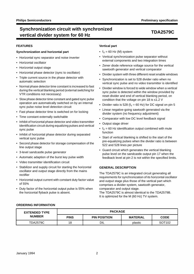
FEATURES
Synchronization and horizontal part
• Horizontal sync separator and noise inverter
• Horizontal oscillator
• Horizontal output stage
• Horizontal phase detector (sync to oscillator)
• Triple current source in the phase detector withautomatic selection
• Normal phase detector time constant is increased to fastduring the vertical blanking period (external switching forVTR conditions not necessary)
• Slow phase detector time constant and gated sync pulseoperation are automatically switched on by an internalsync pulse noise level detection circuit
• Fast phase detector time is switched on for locking
• Time constant externally switchable
• Inhibit of horizontal phase detector and video transmitteridentification circuit during equalizing pulses and verticalsync pulse
• Inhibit of horizontal phase detector during separatedvertical sync pulse
• Second phase detector for storage compensation of theline output stage
• 3-level sandcastle pulse generator
• Automatic adaption of the burst key pulse width
• Video transmitter identification circuit
• Stabilizer and supply circuit for starting the horizontaloscillator and output stage directly from the mainsrectifier
• Horizontal output current with constant duty factor valueof 55%
• Duty factor of the horizontal output pulse is 55% whenthe horizontal flyback pulse is absent.
Vertical part
• fV = 60 Hz (M) system
• Vertical synchronization pulse separator withoutexternal components and two integration times
• Zener diode reference voltage source for the verticalsawtooth generator and vertical comparator
• Divider system with three different reset enable windows
• Synchronization is set to 528 divider ratio when novertical sync pulse and no video transmitter is identified
• Divider window is forced to wide window when a verticalsync pulse is detected within the window provided byreset divider and end of vertical blanking period, oncondition that the voltage on pin 18 is ≤1.2 V
• Divider ratio is 528 (fV = 60 Hz) for DC signal on pin 5
• Linear negative-going sawtooth generated via thedivider system (no frequency adjustment)
• Comparator with low DC level feedback signal
• Output stage driver
• fV = 60 Hz identification output combined with mutefunction
• Start of vertical blanking is shifted to the start of thepre-equalizing pulses when the divider ratio is between522 and 528 lines per picture
• Guard circuit which generates the vertical blankingpulse level on the sandcastle output pin 17 when thefeedback level at pin 2 is not within the specified limits.
GENERAL DESCRIPTION
The TDA2579C is an integrated circuit generating allrequirements for synchronization of its horizontal oscillatorand output stage plus those of the vertical part whichcomprises a divider system, sawtooth generator,comparator and output stage.The TDA2579C is almost identical to the TDA2579B.It is optimized for the M (60 Hz) TV system.
ORDERING INFORMATION
EXTENDED TYPENUMBER
PACKAGE
PINS PIN POSITION MATERIAL CODE
TDA2579C 18 DIL plastic SOT102
January 1994 3
Philips Semiconductors Preliminary specification
Synchronization circuit with synchronizedvertical divider system for 60 Hz
TDA2579C
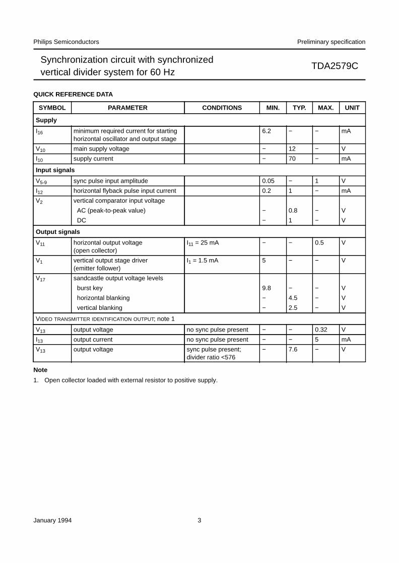
QUICK REFERENCE DATA
Note
1. Open collector loaded with external resistor to positive supply.
SYMBOL PARAMETER CONDITIONS MIN. TYP. MAX. UNIT
Supply
I16 minimum required current for startinghorizontal oscillator and output stage
6.2 − − mA
V10 main supply voltage − 12 − V
I10 supply current − 70 − mA
Input signals
V5-9 sync pulse input amplitude 0.05 − 1 V
I12 horizontal flyback pulse input current 0.2 1 − mA
V2 vertical comparator input voltage
AC (peak-to-peak value) − 0.8 − V
DC − 1 − V
Output signals
V11 horizontal output voltage(open collector)
I11 = 25 mA − − 0.5 V
V1 vertical output stage driver(emitter follower)
I1 = 1.5 mA 5 − − V
V17 sandcastle output voltage levels
burst key 9.8 − − V
horizontal blanking − 4.5 − V
vertical blanking − 2.5 − V
VIDEO TRANSMITTER IDENTIFICATION OUTPUT; note 1
V13 output voltage no sync pulse present − − 0.32 V
I13 output current no sync pulse present − − 5 mA
V13 output voltage sync pulse present;divider ratio <576
− 7.6 − V
January 1994 4
Philips Semiconductors Preliminary specification
Synchronization circuit with synchronizedvertical divider system for 60 Hz
TDA2579C
MG
A79
1
1 nF
9
100
nF
VE
RT
ICA
L/
HO
RIZ
ON
TA
L S
YN
C
SE
PA
RA
TO
R
NO
ISE
IN
VE
RT
ER
CO
INC
IDE
NC
E
DE
TE
CT
OR
PH
AS
E
DE
TE
CT
OR
ϕ1
GA
TIN
G
DIV
IDE
R
VE
RT
ICA
L Z
EN
ER
R
EF
ER
EN
CE
VE
RT
ICA
L C
OM
PA
RA
TO
R
SY
NC
PU
LSE
N
OIS
E L
EV
EL
DE
TE
CT
OR
ϕ1
RE
FE
RE
NC
E
VE
RT
ICA
L B
LAN
KIN
G
VE
RT
ICA
L G
UA
RD
C
IRC
UIT
VE
RT
ICA
L O
UT
PU
T
NO
ISE
D
ET
EC
TO
R
AN
TIT
OP
BU
RS
T
KE
Y
SA
ND
CA
ST
LE
OU
TP
UT
HO
RIZ
ON
TA
L O
SC
ILLA
TO
R
ϕ2
RE
FE
RE
NC
E
FLY
BA
CK
P
ULS
E
PR
OT
EC
TIO
N
PU
LSE
W
IDT
H
MO
DU
LAT
OR
PH
AS
E
DE
TE
CT
OR
ϕ2
TO
O L
OW
C
UR
RE
NT
P
RO
TE
CT
ION
HO
RIZ
ON
TA
L O
UT
PU
T
SU
PP
LY
SW
ITC
H
ST
AR
T
CIR
CU
IT
ST
AB
ILIZ
ER
VID
EO
T
RA
NS
MIT
TE
R
IDE
NT
IFIC
AT
ION
VE
RT
ICA
L/
OS
CIL
LAT
OR
S
AW
TO
OT
H
GE
NE
RA
TO
R
12
1016
158
5
131876
11
4.7
nF
Ω6.
8 k
horiz
onta
l dr
ive
to p
in 1
6
Ω22
0 k
TD
A25
79C
flyba
ck p
ulse
in
put
sand
cast
le
outp
utve
rtic
al
driv
e
vert
ical
fe
edba
ck
150
nFΩ
150
k
to v
ertic
al d
efle
ctio
n cu
rren
t mea
surin
g re
sist
or
43
21
17
22 µF
I
6.2
mA
68 n
F15
0 pF
6.8
µF
Ω1
kΩ
1.2
kvi
deo
sign
al
inpu
t
22 µ FΩ
22
Ω5.
6 k
2.2
µF
47 n
F Ω15
k
mut
e 60
Hz
12 V
Ω33
k
Ω4.
7 k
2.7
nF
12 V
14
R
=S
Fig
.1 B
lock
dia
gram
.
January 1994 5
Philips Semiconductors Preliminary specification
Synchronization circuit with synchronizedvertical divider system for 60 Hz
TDA2579C
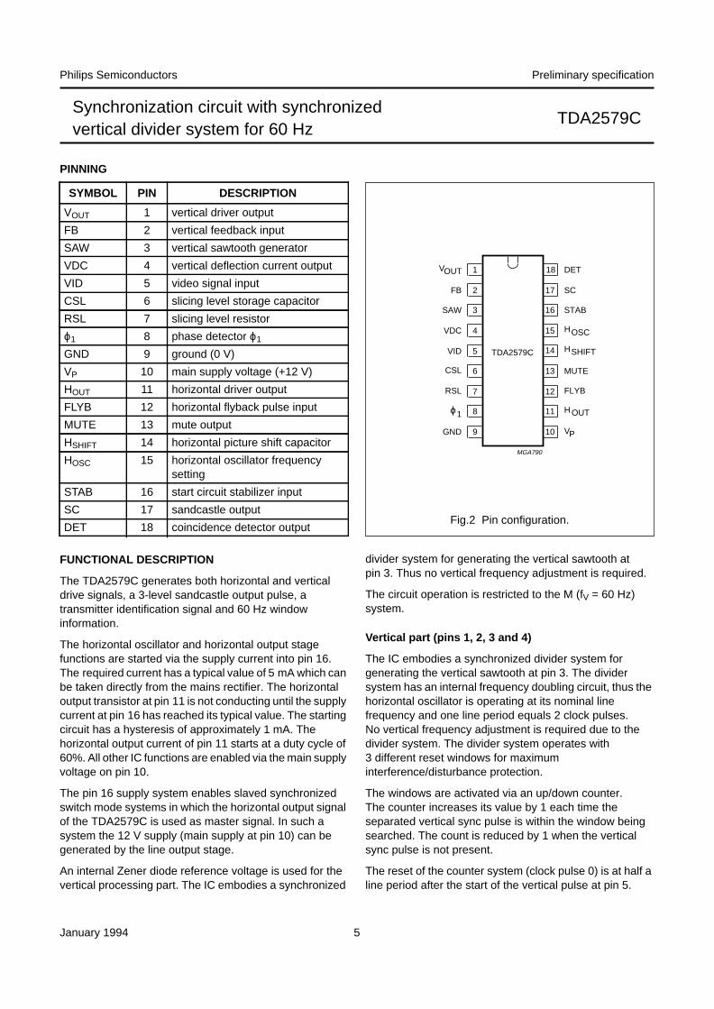
PINNING
SYMBOL PIN DESCRIPTION
VOUT 1 vertical driver output
FB 2 vertical feedback input
SAW 3 vertical sawtooth generator
VDC 4 vertical deflection current output
VID 5 video signal input
CSL 6 slicing level storage capacitor
RSL 7 slicing level resistor
ϕ1 8 phase detector ϕ1
GND 9 ground (0 V)
VP 10 main supply voltage (+12 V)
HOUT 11 horizontal driver output
FLYB 12 horizontal flyback pulse input
MUTE 13 mute output
HSHIFT 14 horizontal picture shift capacitor
HOSC 15 horizontal oscillator frequencysetting
STAB 16 start circuit stabilizer input
SC 17 sandcastle output
DET 18 coincidence detector outputFig.2 Pin configuration.
1
2
3
4
5
6
7
8
9
18
17
16
15
14
13
12
11
10
MGA790
V
FB
SAW
VDC
VID
CSL
RSL
1
GND
DET
SC
STAB
H
SHIFT
MUTE
FLYB
H
VP
ϕ
TDA2579C
OSC
OUT
H
OUT
FUNCTIONAL DESCRIPTION
The TDA2579C generates both horizontal and verticaldrive signals, a 3-level sandcastle output pulse, atransmitter identification signal and 60 Hz windowinformation.
The horizontal oscillator and horizontal output stagefunctions are started via the supply current into pin 16.The required current has a typical value of 5 mA which canbe taken directly from the mains rectifier. The horizontaloutput transistor at pin 11 is not conducting until the supplycurrent at pin 16 has reached its typical value. The startingcircuit has a hysteresis of approximately 1 mA. Thehorizontal output current of pin 11 starts at a duty cycle of60%. All other IC functions are enabled via the main supplyvoltage on pin 10.
The pin 16 supply system enables slaved synchronizedswitch mode systems in which the horizontal output signalof the TDA2579C is used as master signal. In such asystem the 12 V supply (main supply at pin 10) can begenerated by the line output stage.
An internal Zener diode reference voltage is used for thevertical processing part. The IC embodies a synchronized
divider system for generating the vertical sawtooth atpin 3. Thus no vertical frequency adjustment is required.
The circuit operation is restricted to the M (fV = 60 Hz)system.
Vertical part (pins 1, 2, 3 and 4)
The IC embodies a synchronized divider system forgenerating the vertical sawtooth at pin 3. The dividersystem has an internal frequency doubling circuit, thus thehorizontal oscillator is operating at its nominal linefrequency and one line period equals 2 clock pulses.No vertical frequency adjustment is required due to thedivider system. The divider system operates with3 different reset windows for maximuminterference/disturbance protection.
The windows are activated via an up/down counter.The counter increases its value by 1 each time theseparated vertical sync pulse is within the window beingsearched. The count is reduced by 1 when the verticalsync pulse is not present.
The reset of the counter system (clock pulse 0) is at half aline period after the start of the vertical pulse at pin 5.
January 1994 6
Philips Semiconductors Preliminary specification
Synchronization circuit with synchronizedvertical divider system for 60 Hz
TDA2579C
In accordance with the convention for the M system, fieldone line 1 number 1 starts at the first equalizing pulse, thereset of the divider system is at the start of line 4 for the firstfield and in the middle of line 265 for the second field.
Divider system
MODE A: LARGE (SEARCH) WINDOW
Divider ratio between 488 and 576.
This mode is valid for the following five conditions:
1. Divider is locking to a new transmitter.
2. Divider ratio found, not being within the narrow windowlimits.
3. Up/down counter value of the divider system operatingin the narrow window mode decreases below count 1.
4. External forced setting. This can be achieved byloading pin 18 with a 220 Ω resistor to earth or byconnecting a 3.6 V stabistor diode between pin 18 andground.
5. A vertical sync pulse was detected within the intervalprovided by reset divider (at 528) and the end of thevertical blanking while the voltage at pin 18 is ≤1.2 V.
MODE B: NARROW WINDOW
Divider ratio between 522 and 528.
The divider system switches over to this mode when theup/down counter has reached its maximum value of12 approved vertical sync pulses in the large windowmode. When count 12 is reached the vertical sync pulse istested for the standard TV-norm being the divider ratio525. When this value is valid for the 12th vertical pulse, theup/down counter is reset to 0 and the up/down countertests for a valid 525 divider ratio. When at the 12th verticalpulse the divider ratio is not equal to n = 525 then thedivider system remains in the narrow window mode andremains testing for the standard TV-norm. When thedivider operates in this mode and a vertical sync pulse ismissing within the window the divider is reset at the end ofthe window and the counter value is decreased by 1. At acounter value below count 1 the divider system switchesover to the large window mode.
MODE C: STANDARD TV-NORM
Divider ratio 525; fV = 60 Hz.
When the up/down counter has reached its maximumvalue of 12 in the narrow window mode and the dividerratio equals n = 525 the information applied to the up/downcounter is changed such that now the standard dividerratio value is tested and the up/down counter is reset to 0.
When the up/down counter reaches the value of14 approved M TV-norm pulses the divider system ischanged over to the standard divider ratio mode.In this mode the divider is always reset at the standardvalue even if the vertical sync pulse is missing. A missedvertical sync pulse decreases the counter value by 1.When the counter reaches the value of 10 the dividersystem is switched over to the large window mode. Thestandard TV-norm condition provides maximum protectionfor video recorders playing tapes with anti-copy guards.
MODE D: NO TV TRANSMITTER FOUND
At pin 18 the voltage level is less than 1.2 V.
In this condition, only noise is present and no vertical syncpulse is detected, the divider is reset to count 528. In thisway a stable picture display at normal height is achieved.
MODE E: VIDEO TAPE RECORDERS IN FEATURE MODE
NTSC (M system) 3-speed video tape recorders
It should be noted that some VTRs operating in the picturesearch mode, generate such distorted pictures that the noTV transmitter detection circuit can be activated as thevoltage on pin 18 drops below 1.2 V. This would imply arolling picture (Mode D). In general VTRs do use are-inserted vertical pulse in the feature mode. Thereforethe divider system has been designed such that the divideris forced to the wide window mode when V18 is below 1.2 Vand a vertical sync pulse is detected within the windowprovided by the reset divider at 528 and the end of thevertical blanking period.
General
The divider system also generates the anti-top-flutterpulse which inhibits the Phase 1 detector during thevertical sync pulse. The width of this pulse depends on thedivider mode. For the divider mode A the start is generatedat the reset of the divider. In modes B and C theanti-top-flutter pulse starts at the beginning of the firstequalizing pulse sequence. The anti-top-flutter ends afterthe second equalizing pulse sequence.
The vertical blanking pulse is also generated via thedivider system. The start is at the reset of the divider whilethe blanking pulse ends at count 34, the middle of line 21of field 1 and at the end of line 283 of field 2.
The vertical blanking pulse generated at the sandcastleoutput pin 17 is made by adding the anti-top-flutter pulseand the blanking pulse. In this way the vertical blankingpulse starts at the beginning of the first equalizing pulsewhen the divider operates in the B or C mode.
January 1994 7
Philips Semiconductors Preliminary specification
Synchronization circuit with synchronizedvertical divider system for 60 Hz
TDA2579C
Vertical sawtooth
To generate a vertical linear sawtooth voltage a capacitorshould be connected to pin 3. The recommended value is150 nF to 330 nF. The capacitor is charged via an internalcurrent source starting at the reset of the divider system.The voltage on the capacitor is monitored by a comparatorwhich is also activated at reset. When the capacitor hasreached a voltage value of 5.0 V the voltage is keptconstant until the charging period ends. The chargingperiod width is 26 clock pulses. At clock pulse 26 thecomparator is switched off and the capacitor is dischargedby an npn transistor current source the value of which canbe set by an external resistor connected between pin 4and ground (pin 9). Pin 4 is connected to a pnp transistorcurrent source which determines the current of the npncurrent source at pin 3. The pnp current source on pin 4 isconnected to an internal Zener diode reference voltagewhich has a typical voltage of 7.5 V. The recommendedoperating current range is 10 to 75 µA. The resistor atpin 4 should be 100 to 770 kΩ. By using a double currentmirror concept the vertical sawtooth pre-correction voltagecan be set to the required value by external componentsconnected between pins 3 and 4 or by superimposing acorrection voltage in series with the earth connection of theresistor connected to pin 4.The vertical amplitude is set by the current of pin 4.
Vertical feedback
The vertical feedback voltage of the output stage has to beapplied to pin 2. For the normal amplitude adjustment thevalues are DC = 1 V and AC = 0.8 V (p-p).The low DC voltage value improves the picture bouncebehaviour as less parabola compensation is required.Even a DC-coupled feedback circuit is possible.
Vertical guard
The IC also contains a vertical guard circuit. This circuitmonitors the vertical feedback signal on pin 2. When thelevel on pin 2 is below 0.35 V or higher than 1.85 V theguard circuit inserts a continuous voltage level of 2.5 V inthe sandcastle output signal of pin 17. This results inblanking of the picture displayed, thus preventing aburnt-in horizontal line.
Vertical driver output
The driver output is at pin 1, it can deliver a drive currentof 1.5 mA at 5 V output. The internal impedance isapproximately 170 Ω. The output pin is also connected toan internal current source with a sink current of 0.25 mA.
Integration time of the vertical synchronization pulseseparator
The vertical sync separator has two integration times:
• long time; typical 19 µs, valid for 1.8 ≤ V18 ≤ 7.8 V(no noise detected)
• short time; typical 12 µs, valid for noise detected andV18 ≥ 1.2 V.
When V18 drops below 1.2 V, the integration time is forcedback to 19 µs to prevent switching of the divider system tothe wide window mode for noise only conditions.
Sync separator, phase detector and TV-stationidentification (pins 5, 6, 7 and 18)
SYNC SEPARATOR
The video input signal is connected to pin 5. The syncseparator is designed such that the slicing level isindependent of the amplitude of the sync pulse. The blacklevel is measured and stored in the capacitor at pin 7. Theslicing level is stored in the capacitor at pin 6. The slicinglevel value can be chosen by the value of the externalresistor connected between pins 6 and 7. The value isgiven by the formula:
Where RS is the resistor connected between pins 6 and 7and the top sync levels equals 100%. The recommendedresistor value is 5.6 kΩ.
BLACK LEVEL DETECTOR
A gating signal is used for the black level detector. Thissignal is composed of an internal horizontal referencepulse with a duty factor of 50% and the flyback pulse atpin 12. In this way the TV transmitter identificationoperates also for all DC conditions at input pin 5 (no videomodulation, plain carrier only).During the vertical blanking interval the slicing detector isinhibited by a signal which starts with the anti-top-flutterpulse and ends with the reset of the vertical divider circuit.In this way shift of the slicing level due to the vertical syncsignal is reduced and separation of the vertical sync pulseis improved.An internal noise inverter is activated when the video levelat pin 5 decreases below 0.7 V.
pRS
5.3 RS×---------------------- 100 RS value in kΩ( ) .×=
January 1994 8
Philips Semiconductors Preliminary specification
Synchronization circuit with synchronizedvertical divider system for 60 Hz
TDA2579C
NOISE LEVEL DETECTOR
The IC also embodies a built-in sync pulse noise leveldetection circuit. This circuit is directly connected to pin 5and measures the noise level at the middle of thehorizontal sync pulse. When a signal-to-noise level (S/N)of ≤19 dB is detected a counter circuit is activated.
S/N
A video input signal is processed as "acceptable noisefree" when 12 out of 15 sync pulses have a noise levelbelow 19 dB for successive field periods. The sync pulsesare processed during a 15 line width gating periodgenerated by the divider system. The measuring circuithas a built-in noise level hysteresis of approximately 3 dB.The use of a filter of 1 kΩ and 150 pF in front of pin 5reduces the noise content of the CVBS signal byapproximately 6 dB.When the "acceptable noise free" condition is found thephase detector of pin 8 is switched to not gated and normaltime constant. When a higher sync pulse noise level isfound the phase detector is switched over to slow timeconstant and gated sync pulse detection. At the same timethe integration time of the vertical sync pulse separator isreduced providing V18 > 1.2 V.
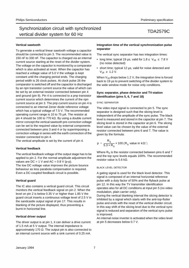
PHASE DETECTOR (SEE FIG.3)
The phase detector circuit is connected to pin 8. Thiscircuit consists of 3 separate phase detectors which areactivated depending on the voltage of pin 18 and the stateof the sync pulse noise detection circuit. For normal andfast time constants all three phase detectors are activatedduring the vertical blanking period, this with the exceptionof the anti-top-flutter pulse period, and the separatedvertical sync pulse time. As a result, phase jumps in thevideo signal related to the video head, take over of videorecorders are quickly restored within the vertical blankingperiod. At the end of the blanking period the phasedetector time constant is increased by a factor of 1.4.In this way there is no requirement for external VTR timeconstant switching, and thus all station numbers aresuitable for signals from VTR, video games or homecomputers.
= 20 logVideo voltage (black-to-white signal)
Noise (RMS)------------------------------------------------------------------------------------------------
For quick locking of a new TV station starting from a noiseonly signal condition (normal time constant) a specialcircuit is incorporated. A new TV station which is notlocked to the horizontal oscillator will result in a voltagedecrease below 0.1 V at pin 18. This will activate a fieldperiod counter which switches the phase detector to fastfor 3 field periods during the vertical scan period.The horizontal oscillator will now lock to the new TV stationand as a result, the voltage on pin 18 will increase toapproximately 6.5 V. When pin 18 reaches a level of 1.8 Vthe mute output transistor of pin 13 is switched off and thedivider is set to the large window. In general the mutesignal is switched off within 5 ms (C18 = 47 nF) afterreception of a new TV signal. When the voltage on pin 18reaches a level of 5 V, usually within 15 ms, the fieldcounter is switched off and the time constant is switchedfrom fast to normal during the vertical scan period.
If the new TV station is weak, the sync noise detector isactivated. This will result in a change over of pin 18 voltagefrom 6.5 V to approximately 10 V. When pin 18 exceedsthe level of 7.8 V the phase detector is switched to slowtime constant and gated sync pulse condition.The phase detector output current during the blankingperiod is now reduced from 2 mA to 1.35 mA.When desired, most conditions of the phase detector canalso be set by external means in the following way:
• fast time constant, TV transmitter identification circuitnot active, connect pin 18 to ground (pin 9)
• fast time constant, TV transmitter identification circuitactive, connect a 220 kΩ resistor between pin 18 andground; this condition can also be set by using a 3.6 Vstabistor diode instead of a resistor
• slow time constant (with the exception of the verticalblanking period), connect pin 18 via a 10 kΩ resistor to+12 V (pin 10); in this condition the transmitteridentification circuit is not active
• no switching to slow time constant required (transmitteridentification circuit active), connect a 6.8 V Zener diodebetween pin 18 and ground.
January 1994 9
Philips Semiconductors Preliminary specification
Synchronization circuit with synchronizedvertical divider system for 60 Hz
TDA2579C
Fig.3 Operation of the three phase detector circuits.
MGA792
mute (pin 13)
gating
1 detectorϕ
voltage (pin 18)
I8 0.35 mA1 detectorϕ
not gatedI8 1.0 mA
2 detectorϕ
not gatedI8 0.65 mA
3 detectorϕ
A B C D E F G
1
0
1
0
1
0
1
0
1
0
0.1 V 1.2 V 1.8 V 3.5 V 5 V 7.8 V
Explanation of areas A to G shown in Fig.3
A switching over to new TV station activates 3 fieldperiod counter
B noise only condition
C TV transmitter identification hysteresis range
D fast time constant
C-E fast time constant hysteresis range
F normal time constant
G sync pulse noise level detection circuit forcespin 18 to >7.8 V while signal-to-noise level<19 dB; slow time constant and gated sync pulseoperation.
Supply (pins 9, 10 and 16)
The IC has been designed such that the horizontaloscillator and output stage operate a very low supplycurrent into pin 16. The horizontal oscillator starts at asupply current of approximately 4 mA (V16 approximately6 V). The horizontal output stage is forced into thenon-conducting stage until the supply current has reacheda typical value of 5 mA.The circuit has been designed such that after starting thehorizontal output function, a current drop of approximately1 mA is allowed.The starting circuit has the ability to derive the main supply(pin 10) from the horizontal output stage. The horizontaloutput signal can also be used as oscillator signal forsynchronized switched-mode power supplies.

January 1994 10
Philips Semiconductors Preliminary specification
Synchronization circuit with synchronizedvertical divider system for 60 Hz
TDA2579C
The maximum allowed starting current is 9.7 mA(Tamb = 25 °C).The main supply should be connected to pin 10 and pin 9should be used for ground. When the voltage on pin 10increases from zero to its final value (typ. 12 V) a part ofthe supply current of the starting circuit is taken from pin 10via internal diodes and the voltage on pin 16 will stabilizeon a typical value of 9.3 V. In stabilized conditions(V10 > 10 V) the minimum required supply current intopin 16 is approximately 2.5 mA.All other IC functions are switched on via the main supplyvoltage on pin 10. When this voltage reaches a value ofapproximately 7 V the horizontal phase detector isactivated and the vertical ramp on pin 3 is started. Thesecond phase detector circuit and burst pulse circuit arestarted when the voltage on pin 10 reaches the stabilizedvoltage value of pin 16 typical 9.3 V.
To close the second phase detector loop a flyback pulsemust be applied to pin 12. When no flyback pulse isdetected the duty factor of the horizontal output stageis 50%.For remote switch-off pin 16 can be connected to ground(via a npn transistor with a collector series resistor ofapproximately 500 Ω) which decreases pin 16 voltage to≤5 V and switches off the horizontal output pulse.
Horizontal oscillator, horizontal output transistor andsecond phase detector
The horizontal oscillator is connected to pin 15. Thefrequency is set by an external RC combination betweenpin 15 and ground (pin 9). The open collector horizontaloutput stage is connected to pin 11. An internal Zenerdiode configuration limits the open voltage of pin 11 toapproximately 14.5 V. The horizontal output transistor atpin 11 is blocked until the current into pin 16 reaches avalue of approximately 5 mA.A higher current results in a horizontal output signal atpin 11, which starts with a duty factor of approximately40% HIGH.The duty factor is set by an internal current-source-loadednpn emitter follower stage connected to pin 14 duringstarting. When pin 16 changes over to voltage stabilizationthe npn emitter follower and current source load at pin 14are switched off and the second phase detector isactivated, provided a horizontal flyback pulse is present atpin 12. When no flyback pulse is detected at pin 12 theduty factor of the horizontal output stage is set to 50%. Thephase detector circuit at pin 14 compensates for storagetime in the horizontal deflection output state.
The horizontal output pulse duration is 29 µs HIGH forstorage times between 1 µs and 17 µs (flyback pulse of12 to 29 µs). A higher storage time increases theHIGH time.Horizontal picture shift is possible by forcing an externalcharge or discharge current into the capacitor at pin 14.
Mute output and 60 Hz identification (pin 13)
The collector of an npn transistor is connected to pin 13.When the voltage on pin 18 drops below 1.2 V (no TVtransmitter) the npn transistor is switched on. When thevoltage on pin 18 increases to a level of approximately1.8 V (new TV transmitter found) the npn transistor isswitched off.This function is available when pin 13 is connected topin 10 (+12 V) via an external pull-up resistor of 10 to20 kΩ. When no TV transmitter is identified the voltage onpin 13 will be LOW (<0.5 V).When an M-system TV transmitter with a divider ratio <576(60 Hz) is found an internal pnp transistor with its emitterconnected to pin 13 will force the output voltage down toapproximately 7.6 V.
Sandcastle output (pin 17)
The sandcastle output pulse generated at pin 17 has threedifferent voltage levels. The highest level (10.4 V) can beused for burst gating and black level clamping. The secondlevel (4.5 V) is obtained from the horizontal flyback pulseat pin 12 and is used for horizontal blanking. The third level(2.5 V) is used for vertical blanking and is derived via thevertical divider system. For 60 Hz the blanking pulseduration is 34 clock pulses started from the reset of thevertical divider system.
For TV signals which have a divider ratio between 522 and528 the vertical blanking pulse is started at the firstequalizing pulse.
January 1994 11
Philips Semiconductors Preliminary specification
Synchronization circuit with synchronizedvertical divider system for 60 Hz
TDA2579C
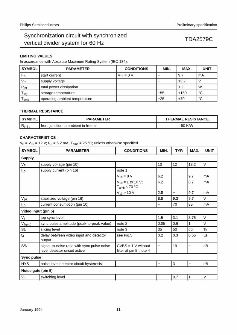
LIMITING VALUESIn accordance with Absolute Maximum Rating System (IEC 134).
THERMAL RESISTANCE
CHARACTERISTICSVP = V10 = 12 V; I16 = 6.2 mA; Tamb = 25 °C; unless otherwise specified.
SYMBOL PARAMETER CONDITIONS MIN. MAX. UNIT
I16 start current V10 = 0 V − 9.7 mA
VP supply voltage − 13.2 V
Ptot total power dissipation − 1.2 W
Tstg storage temperature −55 +150 °CTamb operating ambient temperature −25 +70 °C
SYMBOL PARAMETER THERMAL RESISTANCE
Rth j-a from junction to ambient in free air 50 K/W
SYMBOL PARAMETER CONDITIONS MIN. TYP. MAX. UNIT
Supply
VP supply voltage (pin 10) 10 12 13.2 V
I16 supply current (pin 16) note 1
V10 = 0 V 6.2 − 9.7 mA
V10 = 1 to 10 V;Tamb ≤ 70 °C
6.2 − 8.7 mA
V10 > 10 V 2.5 − 9.7 mA
V16 stabilized voltage (pin 16) 8.8 9.3 9.7 V
I10 current consumption (pin 10) − 70 85 mA
Video input (pin 5)
V5 top sync level 1.5 3.1 3.75 V
V5(p-p) sync pulse amplitude (peak-to-peak value) note 2 0.05 0.6 1 V
SL slicing level note 3 35 50 65 %
td delay between video input and detectoroutput
see Fig.5 0.2 0.3 0.55 µs
S/N signal-to-noise ratio with sync pulse noiselevel detector circuit active
CVBS = 1 V withoutfilter at pin 5; note 4
− 19 − dB
Sync pulse
HYS noise level detector circuit hysteresis − 3 − dB
Noise gate (pin 5)
V5 switching level − 0.7 1 V
January 1994 12
Philips Semiconductors Preliminary specification
Synchronization circuit with synchronizedvertical divider system for 60 Hz
TDA2579C
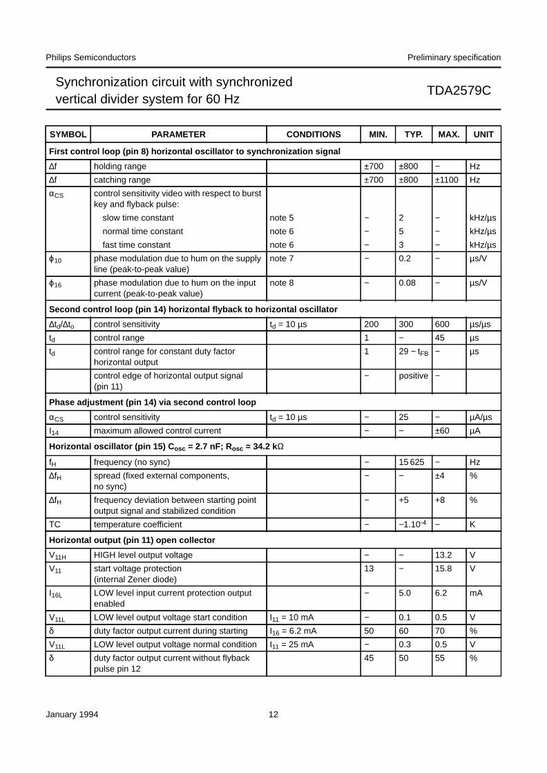
First control loop (pin 8) horizontal oscillator to synchronization signal
∆f holding range ±700 ±800 − Hz
∆f catching range ±700 ±800 ±1100 Hz
αCS control sensitivity video with respect to burstkey and flyback pulse:
slow time constant note 5 − 2 − kHz/µs
normal time constant note 6 − 5 − kHz/µs
fast time constant note 6 − 3 − kHz/µs
ϕ10 phase modulation due to hum on the supplyline (peak-to-peak value)
note 7 − 0.2 − µs/V
ϕ16 phase modulation due to hum on the inputcurrent (peak-to-peak value)
note 8 − 0.08 − µs/V
Second control loop (pin 14) horizontal flyback to horizontal oscillator
∆td/∆to control sensitivity td = 10 µs 200 300 600 µs/µs
td control range 1 − 45 µs
td control range for constant duty factorhorizontal output
1 29 − tFB − µs
control edge of horizontal output signal(pin 11)
− positive −
Phase adjustment (pin 14) via second control loop
αCS control sensitivity td = 10 µs − 25 − µA/µs
I14 maximum allowed control current − − ±60 µA
Horizontal oscillator (pin 15) C osc = 2.7 nF; Rosc = 34.2 kΩ
fH frequency (no sync) − 15 625 − Hz
∆fH spread (fixed external components,no sync)
− − ±4 %
∆fH frequency deviation between starting pointoutput signal and stabilized condition
− +5 +8 %
TC temperature coefficient − −1.10-4 − K
Horizontal output (pin 11) open collector
V11H HIGH level output voltage − − 13.2 V
V11 start voltage protection(internal Zener diode)
13 − 15.8 V
I16L LOW level input current protection outputenabled
− 5.0 6.2 mA
V11L LOW level output voltage start condition I11 = 10 mA − 0.1 0.5 V
δ duty factor output current during starting I16 = 6.2 mA 50 60 70 %
V11L LOW level output voltage normal condition I11 = 25 mA − 0.3 0.5 V
δ duty factor output current without flybackpulse pin 12
45 50 55 %
SYMBOL PARAMETER CONDITIONS MIN. TYP. MAX. UNIT
January 1994 13
Philips Semiconductors Preliminary specification
Synchronization circuit with synchronizedvertical divider system for 60 Hz
TDA2579C
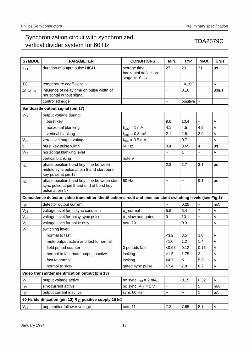
tOH duration of output pulse HIGH storage timehorizontal deflectionstage = 10 µs
27 29 31 µs
TC temperature coefficient − −4.10-2 − K
∆HW/Hd influence of delay time on pulse width ofhorizontal output signal
− 0.16 − µs/µs
controlled edge − positive −
Sandcastle output signal (pin 17)
V17 output voltage during:
burst key 9.8 10.4 − V
horizontal blanking Iload = 1 mA 4.1 4.5 4.9 V
vertical blanking Iload = 0.3 mA 2.1 2.5 2.9 V
V17 zero level output voltage Isink = 0.5 mA − 0.7 − V
tP burst key pulse width 60 Hz 3.4 3.65 4 µs
V12 horizontal blanking level − 1 − V
vertical blanking note 9
td1 phase position burst key time betweenmiddle sync pulse at pin 5 and start burstkey pulse at pin 17
2.3 2.7 3.1 µs
td2 phase position burst key time between startsync pulse at pin 5 and end of burst keypulse at pin 17
60 Hz − − 9.1 µs
Coincidence detector, video transmitter identification circuit and time constant switching levels (see Fig.1)
I18 detector output current − 0.25 − mA
V18 voltage level for in sync condition ϕ1 normal 5.8 6.4 7 V
V18 voltage level for noisy sync pulse ϕ1 slow and gated 9 10.1 − V
V18 voltage level for noise only note 10 − 0.3 − V
V18 switching level:
normal to fast <3.2 3.5 3.8 V
mute output active and fast to normal <1.0 1.2 1.4 V
field period counter 3 periods fast <0.08 0.12 0.16 V
normal to fast mute output inactive locking >1.5 1.75 2 V
fast to normal locking >4.7 5 5.3 V
normal to slow gated sync pulse >7.4 7.8 8.2 V
Video transmitter identification output (pin 13)
V13 output voltage active no sync; I13 = 2 mA − 0.15 0.32 V
I13 sink current active no sync; V13 = 1 V − − 5 mA
I13 output current inactive sync 60 Hz − − 1 µA
60 Hz identification (pin 13) R 13 positive supply 15 k Ω
V13 pnp emitter follower voltage note 11 7.2 7.65 8.1 V
SYMBOL PARAMETER CONDITIONS MIN. TYP. MAX. UNIT
January 1994 14
Philips Semiconductors Preliminary specification
Synchronization circuit with synchronizedvertical divider system for 60 Hz
TDA2579C
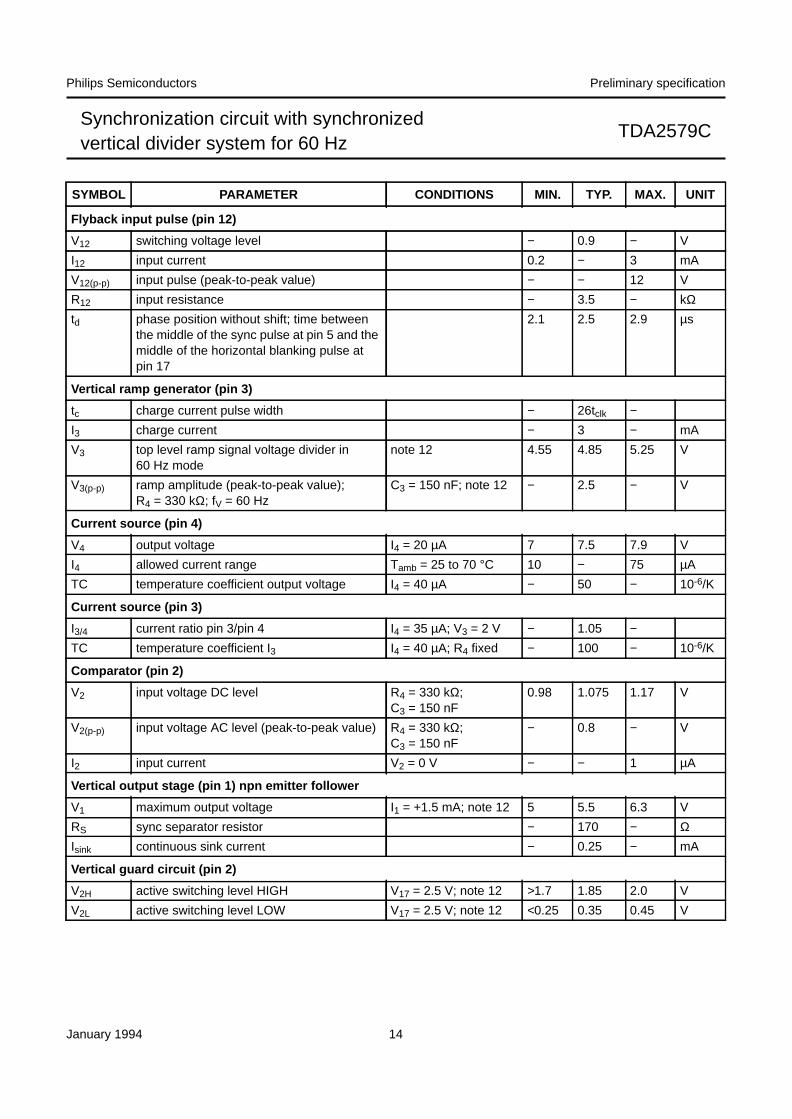
Flyback input pulse (pin 12)
V12 switching voltage level − 0.9 − V
I12 input current 0.2 − 3 mA
V12(p-p) input pulse (peak-to-peak value) − − 12 V
R12 input resistance − 3.5 − kΩtd phase position without shift; time between
the middle of the sync pulse at pin 5 and themiddle of the horizontal blanking pulse atpin 17
2.1 2.5 2.9 µs
Vertical ramp generator (pin 3)
tc charge current pulse width − 26tclk −I3 charge current − 3 − mA
V3 top level ramp signal voltage divider in60 Hz mode
note 12 4.55 4.85 5.25 V
V3(p-p) ramp amplitude (peak-to-peak value);R4 = 330 kΩ; fV = 60 Hz
C3 = 150 nF; note 12 − 2.5 − V
Current source (pin 4)
V4 output voltage I4 = 20 µA 7 7.5 7.9 V
I4 allowed current range Tamb = 25 to 70 °C 10 − 75 µA
TC temperature coefficient output voltage I4 = 40 µA − 50 − 10-6/K
Current source (pin 3)
I3/4 current ratio pin 3/pin 4 I4 = 35 µA; V3 = 2 V − 1.05 −TC temperature coefficient I3 I4 = 40 µA; R4 fixed − 100 − 10-6/K
Comparator (pin 2)
V2 input voltage DC level R4 = 330 kΩ;C3 = 150 nF
0.98 1.075 1.17 V
V2(p-p) input voltage AC level (peak-to-peak value) R4 = 330 kΩ;C3 = 150 nF
− 0.8 − V
I2 input current V2 = 0 V − − 1 µA
Vertical output stage (pin 1) npn emitter follower
V1 maximum output voltage I1 = +1.5 mA; note 12 5 5.5 6.3 V
RS sync separator resistor − 170 − ΩIsink continuous sink current − 0.25 − mA
Vertical guard circuit (pin 2)
V2H active switching level HIGH V17 = 2.5 V; note 12 >1.7 1.85 2.0 V
V2L active switching level LOW V17 = 2.5 V; note 12 <0.25 0.35 0.45 V
SYMBOL PARAMETER CONDITIONS MIN. TYP. MAX. UNIT
January 1994 15
Philips Semiconductors Preliminary specification
Synchronization circuit with synchronizedvertical divider system for 60 Hz
TDA2579C
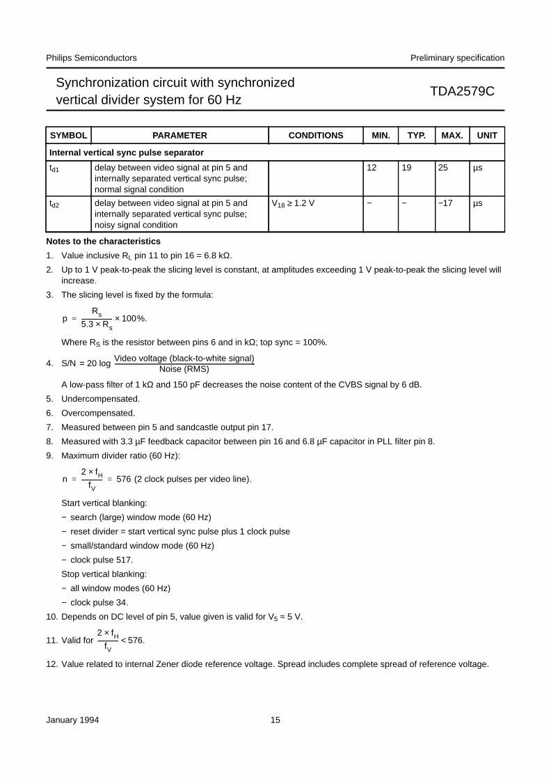
Notes to the characteristics
1. Value inclusive RL pin 11 to pin 16 = 6.8 kΩ.
2. Up to 1 V peak-to-peak the slicing level is constant, at amplitudes exceeding 1 V peak-to-peak the slicing level willincrease.
3. The slicing level is fixed by the formula:
Where RS is the resistor between pins 6 and in kΩ; top sync = 100%.
4. S/N
A low-pass filter of 1 kΩ and 150 pF decreases the noise content of the CVBS signal by 6 dB.
5. Undercompensated.
6. Overcompensated.
7. Measured between pin 5 and sandcastle output pin 17.
8. Measured with 3.3 µF feedback capacitor between pin 16 and 6.8 µF capacitor in PLL filter pin 8.
9. Maximum divider ratio (60 Hz):
Start vertical blanking:
− search (large) window mode (60 Hz)
− reset divider = start vertical sync pulse plus 1 clock pulse
− small/standard window mode (60 Hz)
− clock pulse 517.
Stop vertical blanking:
− all window modes (60 Hz)
− clock pulse 34.
10. Depends on DC level of pin 5, value given is valid for V5 ≈ 5 V.
11. Valid for
12. Value related to internal Zener diode reference voltage. Spread includes complete spread of reference voltage.
Internal vertical sync pulse separator
td1 delay between video signal at pin 5 andinternally separated vertical sync pulse;normal signal condition
12 19 25 µs
td2 delay between video signal at pin 5 andinternally separated vertical sync pulse;noisy signal condition
V18 ≥ 1.2 V − − −17 µs
SYMBOL PARAMETER CONDITIONS MIN. TYP. MAX. UNIT
pRs
5.3 Rs×--------------------- 100%.×=
= 20 logVideo voltage (black-to-white signal)
Noise (RMS)------------------------------------------------------------------------------------------------
n2 fH×
fV-------------- 576 (2 clock pulses per video line).= =
2 fH×fV
-------------- 576.<
January 1994 16
Philips Semiconductors Preliminary specification
Synchronization circuit with synchronizedvertical divider system for 60 Hz
TDA2579C
Fig.4 Counter system.
10
26
34
130
160
488
525
517
528
576
0start
vertical sawtooth charge pulse blocking pulse phase detector 1 vertical blanking
search mode
end of blocking pulse (60 Hz)
end of vertical sawtooth charge pulse
end of vertical blanking (60 Hz)
noise detector window
startblocking pulse phase detector 1 (60 Hz) vertical blanking (60 Hz) normal and narrow window
normal reset
reset divider when mute is active; no vertical sync found
60 Hz identification
search window
MGA793
One video line equals two counter pulses.
Reset counter 32 µs after start of vertical sync pulse at pin 5.
Reset counter = counter state 0.
January 1994 17
Philips Semiconductors Preliminary specification
Synchronization circuit with synchronizedvertical divider system for 60 Hz
TDA2579C
Fig.5 Timing diagram.
Two counter pulses equals one video line.
MGA794
10.4 V
4.5 V
1/2 t FBstorage time horizontal
deflection stage
switching level
video input
separated horizontal sync pulse
horizontal oscillator sawtooth
internal gating pulse
0V
2.5 V
reference
ϕ detector1
output I8
ϕ detector1
ϕ reference level1
2ϕ reference level0.3 sµ
4.7 sµ5-9signal V
horizontal flyback pulse
2.5 sµ
7.5 sµ
3.75 sµ3.75 sµ
coincidence detector
18output I
reference
ϕ detector2
external horizontal
flybackpulse V12-9
output I14
ϕ detector2
29 sµ
horizontal output
signal V11-9
sandcastle output
signal V17-9
0.2 sµ
tP
12 sµ6 sµ 0.7 V
divider in search window mode60 Hz: 34 clock pulses
other divider modes60 Hz: 42 clock pulses
1/2 t FBt FB
January 1994 18
Philips Semiconductors Preliminary specification
Synchronization circuit with synchronizedvertical divider system for 60 Hz
TDA2579C
MG
A79
6
Ω560 Ω880
C
8.4 Ω
k
Ω560 Ω880
C
4.7 Ω
k
Ω560 Ω880
C
2.4 Ω
k
2.4 Ω
k
9.5 Ω
k 4 Ωk
D18
Ωk
Ω36
k
V 2.8
Vre
f
DE
TE
CT
OR
ϕ1
C
A
B
9 Ωk
Ω36
0
5.6 Ω
k
A
6.2 Ω
k
A4.
3 Ωk
SY
NC
SE
PA
RA
TO
R
2 V
ref
eren
ce
0 V
Ω1
k
150
pF
Ω2
kΩ
10 k
A
11 Ωk
10.5 Ω
k
1 Ωk
6 Ωk
B
2 Ωk
3.5 Ω
knois
e de
tect
or
5
VID
EO
IN
PU
T
7.7 Ω
k
Ω1.
5 k
1.3 Ω
kΩ
1.5
k
Ω200
I
Vst
ab
VE
RT
ICA
L S
AW
TO
OT
H G
EN
ER
AT
OR
2.15 Ω
k
Ω2
kI
K
Ω160 Ω150
2 Ωk
µ A25
0
µ A25
0
Ω5.
1 k
Ω1
k
Ω12
k
1.2 Ω
k 12 Ωk
60 H
z id
entif
icat
ion
6 Ωk
11 Ωk 2.
7 Ωk
Ω1.
8 k
1.4
mA
Ω16
0
0.8
mA
1.4
mAΩ
1 k
ϕ 2de
tect
or
stab
ilize
r
5.6 Ω
k
11 Ωk
G
H
pin
16pi
n 10
G
star
t up
Ω3.
9 k
Ω2.
2 kΩ
2.2
k
ϕ2
I
HG
III
pin
16
star
t up
E
F
pin
10
E
FD
Ω220
stab
ilize
r
6.2 Ω
k
DE
TE
CT
OR
ϕ 2H
OR
IZO
NT
AL
OS
CIL
LAT
OR
HO
RIZ
ON
TA
L F
LYB
AC
KH
OR
IZO
NT
AL
OU
TP
UT
VE
RT
ICA
L C
OM
PA
RA
TO
R
Vst
abili
zer
VE
RT
ICA
L D
RIV
ER
C
OIN
CID
EN
CE
DE
TE
CT
OR
T
RA
NS
MIT
TE
R ID
EN
TIF
ICA
TIO
N
SA
ND
CA
ST
LE
SU
PP
LY
12 V
6.8
Ωkpin
16
3.0
mA
0.2
mA
100
nFΩ
33 k
Ω4.
7 k
2.7
nF
Ω1.
2 k
68 n
F
µ F6.
8
Ω22
µF
22µ F
2.2
5.6
Ωk
µF
4.7
3.6 Ω
k
43Ω
k15
0 nF
150 Ω
k
220
Ωk
4.3 Ω
k4.
3 Ωk
100
nF15
Ωk
12 V
TD
A25
79C
43
21
1813
17
91610
1112
1415
87
6
K
Fig
.6 I
nter
nal c
ircui
try
January 1994 19
Philips Semiconductors Preliminary specification
Synchronization circuit with synchronizedvertical divider system for 60 Hz
TDA2579C
Fig.7 TDA2579C and TDA3654 combination 110° Flat Square picture tube.
(1) Dependent on printed-circuit board layout.
MGA795
9
100 nF
1210 1615
8 5
13 14
7 6
11
4.7 nF
sandcastlehorizontal drive
horizontal flyback
150 nF
4 3 2 1
17
22µF
68 nF 6.8µF
Ω1.2 k
video input
22µF
Ω22Ω5.6 k
100 nF
12 V
26 V
18
2.2µF
150 pF
220Ωk
150Ωk
Ωk1
Ω0.5
Ω3.6 k
4.7 µF
TDA2579C
47Ωk
Ω6.8 k
100µF
Ω12 k
Ω39 k
0.2 to 3.0 mA
horizontal shift
2.7 nF
100Ωk
33Ωk
4.7Ωk
f adj.ostart
voltage
6.2 mA to 9.7 mA
transmission identification 60 Hz identification
10 nF
Ω1 k
Ω1 k Ω43 k1000µF
DEFLECTION COIL
Ω270 Ω4.3 k Ω4.3 k
470 pF
(1)
220µF Ω560Ω4.7
100 µF
BAX12
VERTICAL DEFLECTION CIRCUIT TDA3654
9 8 57 6 4 3 2 1
1 nF 10 nF
(1)

January 1994 20
Philips Semiconductors Preliminary specification
Synchronization circuit with synchronizedvertical divider system for 60 Hz
TDA2579C
PACKAGE OUTLINE
Fig.8 18-lead dual in-line; plastic (SOT102).
Dimensions in mm.
8.25 7.80
0.32 max
7.62
9.5 8.3
MSA259
18
1
10
9
1.4 max
6.48 6.14
22.00 21.35
3.7 max 4.7
max
0.51 min
3.9 3.4
seat
ing
plan
e
0.254 M0.53 max
2.54(8x)0.85
max
SOLDERING
Plastic dual in-line packages
BY DIP OR WAVE
The maximum permissible temperature of the solder is260 °C; this temperature must not be in contact with thejoint for more than 5 s. The total contact time of successivesolder waves must not exceed 5 s.
The device may be mounted up to the seating plane, butthe temperature of the plastic body must not exceed thespecified storage maximum. If the printed-circuit board hasbeen pre-heated, forced cooling may be necessaryimmediately after soldering to keep the temperature withinthe permissible limit.
REPAIRING SOLDERED JOINTS
Apply the soldering iron below the seating plane (or notmore than 2 mm above it). If its temperature is below300 °C, it must not be in contact for more than 10 s; ifbetween 300 and 400 °C, for not more than 5 s.

January 1994 21
Philips Semiconductors Preliminary specification
Synchronization circuit with synchronizedvertical divider system for 60 Hz
TDA2579C
DEFINITIONS
LIFE SUPPORT APPLICATIONS
These products are not designed for use in life support appliances, devices, or systems where malfunction of theseproducts can reasonably be expected to result in personal injury. Philips customers using or selling these products foruse in such applications do so at their own risk and agree to fully indemnify Philips for any damages resulting from suchimproper use or sale.
Data sheet status
Objective specification This data sheet contains target or goal specifications for product development.
Preliminary specification This data sheet contains preliminary data; supplementary data may be published later.
Product specification This data sheet contains final product specifications.
Limiting values
Limiting values given are in accordance with the Absolute Maximum Rating System (IEC 134). Stress above one ormore of the limiting values may cause permanent damage to the device. These are stress ratings only and operationof the device at these or at any other conditions above those given in the Characteristics sections of the specificationis not implied. Exposure to limiting values for extended periods may affect device reliability.
Application information
Where application information is given, it is advisory and does not form part of the specification.

January 1994 22
Philips Semiconductors Preliminary specification
Synchronization circuit with synchronizedvertical divider system for 60 Hz
TDA2579C
NOTES
January 1994 23
Philips Semiconductors Preliminary specification
Synchronization circuit with synchronizedvertical divider system for 60 Hz
TDA2579C
NOTES
Philips Semiconductors
Philips Semiconductors – a worldwide companyArgentina: IEROD, Av. Juramento 1992 - 14.b, (1428)
BUENOS AIRES, Tel. (541)786 7633, Fax. (541)786 9367Australia: 34 Waterloo Road, NORTH RYDE, NSW 2113,
Tel. (02)805 4455, Fax. (02)805 4466Austria: Triester Str. 64, A-1101 WIEN, P.O. Box 213,
Tel. (01)60 101-1236, Fax. (01)60 101-1211Belgium: Postbus 90050, 5600 PB EINDHOVEN, The Netherlands,
Tel. (31)40 783 749, Fax. (31)40 788 399Brazil: Rua do Rocio 220 - 5th floor, Suite 51,
CEP: 04552-903-SÃO PAULO-SP, Brazil.P.O. Box 7383 (01064-970).Tel. (011)829-1166, Fax. (011)829-1849
Canada: INTEGRATED CIRCUITS:Tel. (800)234-7381, Fax. (708)296-8556DISCRETE SEMICONDUCTORS: 601 Milner Ave,SCARBOROUGH, ONTARIO, M1B 1M8,Tel. (0416)292 5161 ext. 2336, Fax. (0416)292 4477
Chile: Av. Santa Maria 0760, SANTIAGO,Tel. (02)773 816, Fax. (02)777 6730
Colombia: Carrera 21 No. 56-17, BOGOTA, D.E., P.O. Box 77621,Tel. (571)217 4609, Fax. (01)217 4549
Denmark: Prags Boulevard 80, PB 1919, DK-2300 COPENHAGEN S,Tel. (032)88 2636, Fax. (031)57 1949
Finland: Sinikalliontie 3, FIN-02630 ESPOO,Tel. (9)0-50261, Fax. (9)0-520971
France: 4 rue du Port-aux-Vins, BP317,92156 SURESNES Cedex,Tel. (01)4099 6161, Fax. (01)4099 6427
Germany: P.O. Box 10 63 23, 20095 HAMBURG ,Tel. (040)3296-0, Fax. (040)3296 213
Greece: No. 15, 25th March Street, GR 17778 TAVROS,Tel. (01)4894 339/4894 911, Fax. (01)4814 240
Hong Kong: 15/F Philips Ind. Bldg., 24-28 Kung Yip St.,KWAI CHUNG, Tel. (0)4245 121, Fax. (0)4806 960
India: PEICO ELECTRONICS & ELECTRICALS Ltd.,Components Dept., Shivsagar Estate, Block 'A',Dr. Annie Besant Rd., Worli, BOMBAY 400 018,Tel. (022)4938 541, Fax. (022)4938 722
Indonesia: Philips House, Jalan H.R. Rasuna Said Kav. 3-4,P.O. Box 4252, JAKARTA 12950,Tel. (021)5201 122, Fax. (021)5205 189
Ireland: Newstead, Clonskeagh, DUBLIN 14,Tel. (01)640 000, Fax. (01)640 200
Italy: Viale F. Testi, 327, 20162 MILANO,Tel. (02)6752.1, Fax. (02)6752.3350
Japan: Philips Bldg 13-37, Kohnan 2 -chome, Minato-ku, KOKIO 108,Tel. (03)3740 5101, Fax. (03)3740 0570
Korea: (Republic of) Philips House, 260-199 Itaewon-dong,Yongsan-ku, SEOUL, Tel. (02)794-5011, Fax. (02)798-8022
Malaysia: No. 76 Jalan Universiti, 46200 PETALING JAYA,SELANGOR, Tel. (03)757 5511, Fax. (03)757 4880
Mexico: Philips Components, 5900 Gateway East, Suite 200,EL PASO, TX 79905, Tel. 9-5(800)234-7381, Fax. (708)296-8556
Netherlands: Postbus 90050, 5600 PB EINDHOVEN,Tel. (040)78 37 49, Fax. (040)78 83 99
New Zealand: 2 Wagener Place, C.P.O. Box 1041, AUCKLAND,Tel. (09)849-4160, Fax. (09)849-7811
Norway: Box 1, Manglerud 0612, OSLO,Tel. (22)74 8000, Fax. (22)74 8341
Pakistan: Philips Markaz, M.A. Jinnah Rd., KARACHI 3,Tel. (021)577 039, Fax. (021)569 1832
Philippines: PHILIPS SEMICONDUCTORS PHILIPPINES Inc,106 Valero St. Salcedo Village, P.O. Box 911, MAKATI,Metro MANILA, Tel. (02)810 0161, Fax. (02)817 3474
Portugal: Av. Eng. Duarte Pacheco 6, 1009 LISBOA Codex,Tel. (01)683 121, Fax. (01)658 013
Singapore: Lorong 1, Toa Payoh, SINGAPORE 1231,Tel. (65)350 2000, Fax. (65)251 6500
South Africa: 195-215 Main Road, Martindale,P.O. Box 7430,JOHANNESBURG 2000,Tel. (011)470-5433, Fax. (011)470-5494
Spain: Balmes 22, 08007 BARCELONA,Tel. (03)301 6312, Fax. (03)301 42 43
Sweden: Kottbygatan 7, Akalla. S-164 85 STOCKHOLM,Tel. (0)8-632 2000, Fax. (0)8-632 2745
Switzerland: Allmendstrasse 140, CH-8027 ZÜRICH,Tel. (01)488 2211, Fax. (01)481 7730
Taiwan: 69, Min Sheng East Road, Sec 3, P.O. Box 22978,TAIPEI 10446, Tel. (2)509 7666, Fax. (2)500 5899
Thailand: PHILIPS ELECTRONICS (THAILAND) Ltd.,60/14 MOO 11, Bangna - Trad Road Km. 3Prakanong, BANGKOK 10260,Tel. (2)399-3280 to 9, (2)398-2083, Fax. (2)398-2080
Turkey: Talatpasa Cad. No. 5, 80640 LEVENT/ISTANBUL,Tel. (0212)279 2770, Fax. (0212)269 3094
United Kingdom: Philips Semiconductors Limited, P.O. Box 65,Philips House, Torrington Place, LONDON, WC1E 7HD,Tel. (071)436 41 44, Fax. (071)323 03 42
United States: INTEGRATED CIRCUITS:811 East Arques Avenue, SUNNYVALE, CA 94088-3409,Tel. (800)234-7381, Fax. (708)296-8556DISCRETE SEMICONDUCTORS: 2001 West Blue Heron Blvd.,P.O. Box 10330, RIVIERA BEACH, FLORIDA 33404,Tel. (800)447-3762 and (407)881-3200, Fax. (407)881-3300
Uruguay: Coronel Mora 433, MONTEVIDEO,Tel. (02)70-4044, Fax. (02)92 0601
For all other countries apply to: Philips Semiconductors,International Marketing and Sales, Building BAF-1,P.O. Box 218, 5600 MD, EINDHOVEN, The Netherlands,Telex 35000 phtcnl, Fax. +31-40-724825
SCD27 © Philips Electronics N.V. 1993
All rights are reserved. Reproduction in whole or in part is prohibited without theprior written consent of the copyright owner.
The information presented in this document does not form part of any quotationor contract, is believed to be accurate and reliable and may be changed withoutnotice. No liability will be accepted by the publisher for any consequence of itsuse. Publication thereof does not convey nor imply any license under patent- orother industrial or intellectual property rights.
Printed in The Netherlands 9397 725 20011