Embed Size (px)
Citation preview

https://daffy1108.wordpress.com/2014/06/08/synchronizers-for-asynchronous-signals/ Synchronizers for Asynchronous Signals Asynchronous signals causes the big issue with clock domains, namely metastability. This is a situation where the clock domain trying to capture the asynchronous event goes into a metastable state. Is the asychronous signal a logic “1” or a logic “0” state? Metastability cannot be prevented but it can be reduce. High-speed digital circuits rely on synchronizers to create a time buffer for recovering from a metastable event, thereby reducing the possibility that metastability will cause a circuit to malfunction. EDA companies such as Synopsys, Cadence and Mentor Graphics, create software to automatically read verilog code and detect synchronization problems. There are two basic types of synchronizers: 1) Asynchronous signal wider than the clock period of the synchronizer clock domain and 2) Asynchronous signal smaller than the clock period of the synchronizer clock domain.
Asynchronous signal > Synchronizer clock period If designed into an ASIC (Application Specific Integrated Circuit), this synchronizer is typically put into a special library cell to keep the two back to back D flip-flop close to each other functionally and to minimize any clock skew in the ASIC. In addition, as a rule of thumb, this synchronizer usually has a special cell name like “sync_ss”, meaning synchronize slow input signal.
1
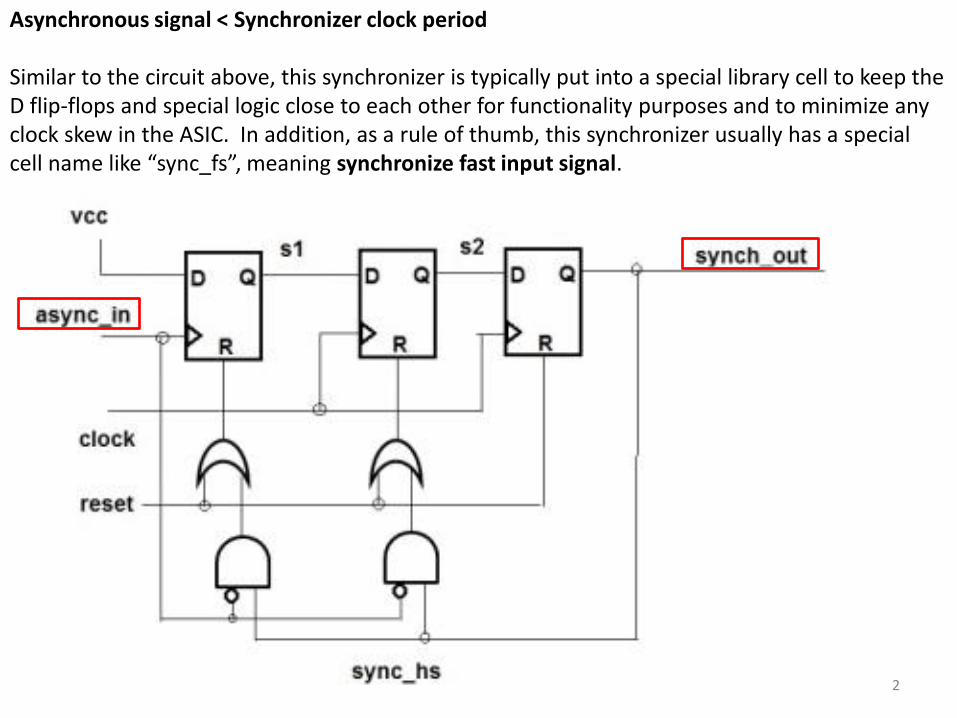
Asynchronous signal < Synchronizer clock period Similar to the circuit above, this synchronizer is typically put into a special library cell to keep the D flip-flops and special logic close to each other for functionality purposes and to minimize any clock skew in the ASIC. In addition, as a rule of thumb, this synchronizer usually has a special cell name like “sync_fs”, meaning synchronize fast input signal.
2

https://inst.eecs.berkeley.edu/~cs150/sp10/Collections/Papers/ClockCrossing.pdf AS DIGITAL DESIGN BECOMES INCREASINGLY SOPHISTICATED, CIRCUITS WITH MULTIPLE CLOCKS MUST RELIABLY COMMUNICATE WITH EACH OTHER When signals travel from one clock domain to another, the signal appears to be asynchronous in the new clock domain. The circuit that receives this signal needs to synchronize it. Synchronization prevents the metastable state of the first storage element (flip-flop) in the new clock domain from propagating through the circuit. Metastability is the inability of a flip-flop to arrive at a known state in a specific amount of time. When a flip-flop enters a metastable state, you can predict neither the element’s output voltage level nor when the output will settle to a correct voltage level. During this settling time, the flip-flop’s output is at some intermediate voltage level or may oscillate and can cascade the invalid output level to flip-flops farther down the signal path. The input must be stable during a small window of time around the active edge of the clock for any flip-flop. FPGA manufacturers and IC foundries qualify their flip-flops and determine their characteristics. “MTBF”(mean time between failures) describes the metastability characteristic of a flip-flop using statistics to determine the probability of a flip-flop’s failure. Manufacturers base the MTBF in part on the length of the time window during which a change in the input signal causes the flip-flop to become unstable. In addition, MTBF calculation uses the frequency of the input signal and the frequency of the clock driving the flip-flop.
3

Each type of flip-flop in an ASIC or FPGA library has timing requirements to help you determine the window of vulnerability. “Setup time” describes the time an input signal to a flip-flop must be stable before the clock edge. “Hold time” is the time the signal must remain stable after the clock edge. These specifications are usually conservative to account for all the possible variations in supply voltage, operating temperature, signal quality, and fabrication. If a design meets these timing requirements, the possibility is negligible that the flip-flop will fail. Synthesis programs in modern IC and FPGA designs ensure that digital circuits meet the setup-and-hold requirements for each flip-flop in the design; however, asynchronous signals pose problems for the software. A signal crossing a clock domain appears to be asynchronous to the logic in the new clock domain. SIGNAL SYNCHRONIZATION The purpose of synchronizing signals is to protect downstream logic from the metastable state of the first flip-flop in a new clock domain. A simple synchronizer comprises two flip-flops in series without any combinational circuitry between them. This design ensures that the first flip-flop exits its metastable state and its output settles before the second flip-flop samples it. You also need to place the flip-flops close to each other to ensure the smallest possible clock skew between them. IC foundries help with signal synchronization by providing synchronizer cells. These cells usually comprise a flip-flop with a very high gain that uses more power and is larger than a standard flip-flop. Such a flip-flop has reduced setup-and hold-time requirements for the input signal and is resistant to oscillation when the input signal causes a metastable condition.
4

For synchronization to work properly, the signal crossing a clock domain should pass from flip-flop in the original clock domain to the first flip-flop of the synchronizer without passing through any combinational logic between the two. This requirement is important because the first stage of a synchronizer is sensitive to glitches that combination logic produces. A synchronized signal is valid in the new clock domain after two clock edges. The signal delay is between one and two clock periods in the new clock domain. A rule of thumb is that a synchronizer circuit causes two clock cycles of delay in the new clock domain.
5

The edge-detecting synchronizer circuit adds a flip-flop to the output of the level synchronizer.
This circuit detects the rising edge of the input to the synchronizer and generates a clockwide, active-high pulse. Switching the inverter on the AND gate inputs creates a synchronizer that detects the falling edge of the input signal. Changing the AND gate to a NAND gate results in a circuit that generates an active-low pulse. The edge-detecting synchronizer works well at synchronizing a pulse going to a faster clock domain. This circuit produces a pulse that indicates the rising or falling edge of the input signal. One restriction of this synchronizer is that the width of the input pulse must be greater than the period of the synchronizer clock plus the required hold time of the first synchronizer flip-flop. The safest pulse width is twice the synchronizer clock period. This synchronizer does not work if the input is a single clock wide pulse entering a slower clock domain.
6

The input signal of a pulse synchronizer is a single clockwide pulse that triggers a toggle circuit in the originating clock. The output of the toggle circuit switches from high to low and vice versa each time it receives a pulse and passes through the level synchronizer to arrive at one input of the XOR gate, while a one-clock-cycle-delayed version goes to the other input of the XOR. For one clock cycle, each time the toggle circuit changes state, the output of this synchronizer generates a single clockwide pulse.
The basic function of a pulse synchronizer is to take a single clockwide pulse from one clock domain and create a single clockwide pulse in the new domain. One restriction of a pulse synchronizer is that input pulses must have a minimum spacing between pulses equal to two synchronizer clock periods. If the input pulses are closer, the output pulses in the new clock domain are adjacent to each other, resulting in an output pulse that is wider than one clock cycle. This problem is more severe when the clock period of input pulse is greater than twice the synchronizer clock period. In this case, if the input pulses are too close, the synchronizer does not detect every one.
7

8
https://web.stanford.edu/class/ee183/handouts_spr2003/synchronization_pres.pdf

9

10
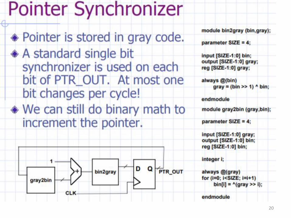
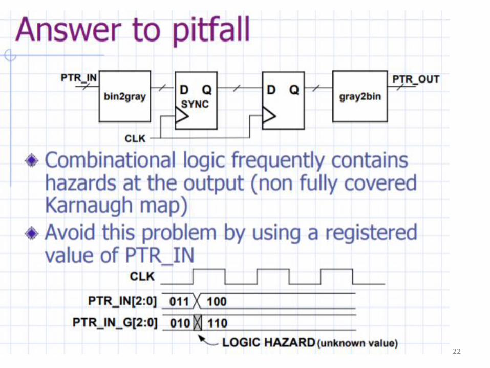
Bus Synchronization Obvious approach is to use single signal synchronizers on each bit : WRONG! Handshaking is the Answer

11

12

13

14

15

16

17

18

19
20

21
22

23

24

25
https://moodle.epfl.ch/pluginfile.php/466321/mod_resource/content/0/Presentation_ES_A2008/DFF_Synchronization.pdf
Some synchronization problems with logic in FPGA Problem to solve: If an external asynchronous signal is used inside a synchronous system it needs to be synchronized before use. Why ? 1. Metastability problem 2. At the same clk sampling time (i.e. rising_edge(Clk)), all the logic elements using this signal
and clocking it, need to see it at the same logical level !! Metastability problem: To be correctly sampled by a FF (Flip-Flop or D-register) a signal (D) needs to respect 2 very important timings: • tsu: Set up time: D valid before ↑Clk • thold: Hold time: D stay valid after ↑Clk

26
If the rule is NOT respected: • The output can be '0' or '1' good • The output can be in an intermediate level for an undefined time metastable level
DFF.. Sampling of input signals • The level of the metastable signal is between the '0' and the '1'. • The time the metastable signal stays is probabilistic and theoretically could be infinitive. Practically it disappears at the next signal sampling. • Usually a DFF sampling a metastable level would not propagate it. As for this intermediate level, a decision is take for a '0' or a '1'. • It could propagate to a next DFF if the level change just at the sampling point to the metastable threshold, the probability is very low but not 0 ! • Thus depending on the hardness of the design to do, more DFF are needed. Manufacturer provides information about the parameters for metastability.

27
DFF.. Sampling of input signals View of the same value for all the sampling FF. If the rule is NOT respected: • Very bad for 1 DFF worst if the same signal D is going to more than 1 DFF: • each DFF could see a different input level Qa, Qb : 2 different DFF outputs

28
DFF.. Sampling of input signals At the same clk sampling time (i.e. rising_edge), all the logics using the signal and clocking it, need to see it at the same logic level !! A synchronizing system is necessary

29
DFF.. Sampling of input signals The first DFF can have a metastable signal as output Qm The second one will probably filter it For very high reliability system more DFF could be necessary, delay added !!
DFF.. Sampling of input signals The Qsn signal can be used by all the logic that need it: the level will be the same for all the logic elements
Async Input

30
DFF.. Sampling of input signals Clock distribution Inside the FPGA all the DFF using the same D signal need to use the same Clock. Special global lines are available inside a FPGA for that purpose. They are limited in number. If we expect to use a normal signal as a clock for a FF it's a very bad idea We need to use the Clock Enable feature of a DFF in a FPGA
DFF.. Conclusion Asynchronous signals need to be synchronized before use in a FPGA
A simple DFF can generate metastable output
At least a second DFF is necessary to filter this metastable signal

31
http://www2.elo.utfsm.cl/~lsb/elo211/aplicaciones/katz/chapter6/chapter06.doc4.html The Problem of Asynchronous Inputs Sometimes asynchronous inputs cannot be avoided for example, when a signal must pass from the outside world into the synchronous system. An example might be a reset signal, triggered by an operator pressing a push-button. It is particularly dangerous to fan out an asynchronous input to many points in the clocked system: if the input changes close to the clock event, it may be seen at some flip-flops but not others, leading to an "impossible" state. An incorrect circuit for handling an asynchronous input is shown in Figure Two positive edge-triggered D flip-flops are driven by the same asynchronous input. You would expect both devices to hold the same state, yet because of different wiring and other internal delays, one flip-flop is set while the other remains reset. The assumption that both flip-flops hold the same state is now invalid.


![PLSQL.ppt [modalità compatibilità]bias.csr.unibo.it/golfarelli/LabDB/MaterialeDidattico/13-PLSQL.pdf · IllinguaggioproceduraleperlIl linguaggio procedurale per lestensione’estensionedel](https://img.pdfslide.net/doc/110x75/5c66901909d3f2d0218c7ba8/plsqlppt-modalita-compatibilitabiascsruniboitgolfarellilabdbmaterialedidattico13-plsqlpdf.jpg)


![web2.ppt [Sola lettura] - biblioteca.asmn.re.itbiblioteca.asmn.re.it/allegati/MaterialeDidattico/Vanna Pistotti.pdf · Microsoft PowerPoint - web2.ppt [Sola lettura] Author: rossii](https://img.pdfslide.net/doc/110x75/60012ce70adebd0a0159f154/web2ppt-sola-lettura-pistottipdf-microsoft-powerpoint-web2ppt-sola-lettura.jpg)