Embed Size (px)
Citation preview

Hindawi Publishing CorporationAdvances in Optical TechnologiesVolume 2008, Article ID 315724, 8 pagesdoi:10.1155/2008/315724
Research ArticleSynthesis of Planar Reflective Gratings forSilicon Interconnects
Ronald Millett, Jamie Ramsey, Przemek Bock, Julie Nkanta, Henry Schriemer,Trevor J. Hall, and Serge Bidnyk
School of Information Technology and Engineering, University of Ottawa, Ottawa, Canada ON K1N 6N5
Correspondence should be addressed to Ronald Millett, [email protected]
Received 29 November 2007; Accepted 13 March 2008
Recommended by Pavel Cheben
The design and simulations of planar reflective gratings for building optical interconnects in silicon-on-insulator (SOI) werestudied for a range of silicon core thicknesses of 0.1 to 10 μm. The verticality of the grating facets has been shown to be the maincontributing factor to the cumulative crosstalk in thick silicon cores. The dispersion property of the slab was found to limit theminimal thickness of the core for polarization-insensitive gratings. The effects of polarization-dependent confinement on opticalcrosstalk were studied. The findings were used to design and simulate a polarization-insensitive 18-channel coarse wavelengthdivision demultiplexer (CWDM) with a free spectral range of over 600 nm. The CWDM demultiplexer uses a 1.7 μm silicon coreand combines a shallow-etch tapered rib structure and multimode silicon channels to produce box-like passbands for integratedreceiver applications. The diffraction grating was constructed using double astigmatic point design with phase-corrected gratingfacets to reduce astigmatism. Optical properties of the planar gratings have been simulated using quasivectorial diffraction gratingtheory. The simulation results confirm that there is high diffraction efficiency and low optical crosstalk over the entire range ofoperation. Applications of planar silicon gratings to the synthesis of silicon interconnects are discussed.
Copyright © 2008 Ronald Millett et al. This is an open access article distributed under the Creative Commons Attribution License,which permits unrestricted use, distribution, and reproduction in any medium, provided the original work is properly cited.
1. INTRODUCTION
Over the past several decades, data transfer rates overelectronic interconnects have been increasing exponentiallyfollowing Moore’s law. The clock speed of silicon-basedelectronic processors has reached microwave frequencies ofover 4 GHz causing severe problems with the signal integrityof electronic interconnects. At these frequencies, traditionalstripline interconnects suffer from a fundamental cross-coupling penalty and large radiation losses. The researchin silicon photonics has been driven primarily by theobjective of overcoming the limitations of stripline inter-connects. Recently, several key elements, including siliconlasers, modulators, and photodetectors, have been realizedin silicon using low-cost CMOS-compatible processes [1,2]. Further research in silicon-on-insulator (SOI) showspromise for implementing additional key functionality—demultiplexing—to enable wavelength division multiplexingand transferring data over multiple channels. The highindex contrast of SOI waveguides also permits smaller
device footprints compared to more weakly guided materialsystems.
Due to performance limitations, arrayed waveguidegrating- (AWG-) based demultiplexers in SOI have not beenable to compete effectively with silica-based AWGs. PortingAWG technology directly from silica to SOI has been achallenge, mainly due to high waveguide propagation losses,limited spectral range, strong polarization dependence, andpoor optical crosstalk arising from phase noise in the delayline region of SOI-based AWGs [3]. In order to overcomeAWG limitations in SOI, several research groups haveexplored the possibility of using planar reflective gratingsas an alternative to AWGs. To generate diffraction, planarreflective gratings, also known as Echelle gratings, rely on theoptical properties of a 2D silicon slab as opposed to a phasearray of waveguides in AWGs. SOI-based planar reflectivegratings have now been realized with SOI core thicknessesof 0.22 μm [4], 3 μm [5], and 5 μm [6]. These initial studiesare very promising and demonstrate that on-chip insertion

2 Advances in Optical Technologies
losses of less than 2 dB are readily achievable in both thinand thick core SOI-based planar gratings [4, 5].
In this paper, we theoretically explore the opticalproperties of planar reflective grating demultiplexers basedon silicon cores of various thicknesses. We show thatthe thickness of the silicon core layer has a profoundeffect on the polarization and crosstalk performance ofthe SOI grating. The results of our findings were usedto synthesize a polarization-insensitive 18-channel coarsewavelength division demultiplexer (CWDM) with box-likeresponses based on a planar reflective grating. The devicecombines a shallow-etch tapered rib structure and multi-mode silicon channels. The grating was optimized to reduceaberration effects. The polarization-insensitive performanceof the demultiplexer was confirmed using quasi-vectorialdiffraction theory. Applications of planar reflective gratingsto building silicon interconnects are discussed.
2. PLANAR REFLECTIVE GRATING DESIGN
The success of AWGs in meeting the requirements of themultichannel demultiplexer market has been largely due tothe silica platform where AWGs can be fabricated usingshallow etched waveguides in a relatively simple fabrica-tion process. In spite of a considerably smaller footprint,the fabrication of planar reflective gratings in silica wasmore complex compared to AWGs and required additionalresearch into controlling the verticality and smoothness ofthe reflective facets. Contrary to silica, there are a numberof well-established processes for producing deep, smooth,and highly vertical-etched structures in SOI. One of thekey advantages of planar grating devices compared to free-space bulk gratings is that they are lithographically producedand any grating shape is readily achievable. Techniques foretching silicon have benefited from recent advancements inthe fabrication of microelectromechanical systems. Planarreflective gratings in SOI have the potential for monolithicintegration with large-scale electronic-integrated circuits.
An SOI-based planar grating uses a variety of input andoutput structures, as shown in Figure 1. In a rib-waveguideSOI structure, the fundamental mode of the waveguide isasymmetrically positioned below the center of the slab core.In order to improve the waveguide-to-slab coupling, theinput waveguide is usually tapered at the entrance to the slabregion. In the slab, the light remains confined in the verticaldirection but expands horizontally until it encounters a seriesof reflectors. The grating not only diffracts but also refocusesthe light into the output waveguides, as shown in Figure 1.
The lithographic approach to making planar gratingscarries little design restrictions on the shape of the launchingmode or the shapes of the diffracting elements. Suchflexibility in planar grating design has recently resulted in thesuccessful demonstration of planar gratings with facet widthsvarying from 4 to 1000 μm [4, 7]. Diffractive elements in SOIcan be created by either a single dielectric-to-metal interface[5], a reflective dielectric stack [8], or using total-internalreflection facets [6].
The first planar reflective gratings were realized usingthe Rowland configuration [9]. Research into novel grating
Inpu
t
Ou
tpu
ts
Shallow etch
I
O1
Oi
λ1
λi
EllipticalFacets
Xi
Deep etch
Figure 1: Architecture of the planar reflective grating in a silicon-on-insulator optical interconnect. A shallow etch (0.5 μm) definesthe input structure, whereas a deep etch (1.7 μm) defines the outputwaveguides and grating facets.
designs has since yielded a methodology for eliminating theaberration effects caused by grating facets [10]. Subsequently,a mechanism of compensating for the dispersion of therefractive index of glass has been discovered, resulting in thesuccessful demonstration of interleavers [7].
A comparative analysis of both planar reflective gratingsand arrayed waveguide gratings recently performed byCheben found that the traditional scalar approach to thesimulation of planar gratings is unable to reconcile simulatedand measured data [11]. Numerical difficulties posed bythe large number of diffraction orders, deep triangulargrooves with high blaze angles, and small wavelength-to-grating pitch ratios have made the calculation of diffractionefficiency one of the most intractable problems of electro-magnetic theory.
Until a decade ago, simple relationships between funda-mental grating parameters, such as diffraction order, diffrac-tion angle, resolving power, Rowland circle radius, gratingpitch, were deemed sufficient to model planar reflectivegratings. The linear dispersion strength of a planar gratingcan be readily computed through the angle of incidence, α,and reflected angle, α′ [12]:
L∂α′
∂λ= L
sinα + sinα′
λcos α′
[1− λ
n
∂n
∂λ
], (1)
where L is the length of the slab region. Theoretically, it ispossible to use infinite permutations of diffraction angles andslab lengths to produce gratings with almost identical charac-teristics. However, in practice, researchers have realized thattheoretically equivalent gratings can exhibit vastly differentperformance characteristics.
Vector diffraction theories that replaced the traditionalscalar approach revealed that the shape and metallizationof the grating facets affect both the grating efficiency andpolarization sensitivity. Delage and Dossou [13] solvedMaxwell’s equations in proximity to the grating facets using afinite-element method and matched their numerical solutionnear the grating surface to a Rayleigh expansion. Their workshowed that metallization had a profound impact on theabsolute and relative grating efficiencies of both TE and TMpolarized light.

Ronald Millett et al. 3
The design of planar gratings in SOI requires carefulstudies on the effects of silicon core thickness and grating ver-ticality on the polarization dependence and optical crosstalk.Particular consideration should be given to the selection ofdiffraction angles for the planar grating in SOI.
3. POLARIZATION DEPENDENCE OFPLANAR GRATINGS
The polarization dependence of the wavelength (PDW) hasdifferent origins in AWGs and planar reflective gratings.PDW in an SOI-based AWG is predominantly caused bywaveguide birefringence in the phase array region. Con-tributing factors to the waveguide birefringence includewaveguide cross-section variations and stress. Both of thesefactors can be used to eliminate modal birefringence in SOI-ridge waveguides [14]. Consequently, the selection of properwaveguide dimensions and cladding layers is essential forimproving the PDW performance of AWGs.
Contrary to AWGs, the PDW of SOI planar waveguidegratings depends only on birefringence of the slab and notthe waveguides. The geometry of waveguides can be selectedindependently, thus providing additional design flexibility inoptimizing other planar lightwave circuit subcomponents,such as fiber-to-waveguide mode converters and bend waveg-uide regions.
The modes of an asymmetric slab waveguide can befound using analytical expressions that assume that thewaveguide is infinite in the transverse direction [15]. Thethree layers of the infinite asymmetric slab waveguide area cladding layer of air (n0 = 1), a core layer of silicon(n1 = 3.48), and a substrate layer of SiO2(n2 = 1.445). Thethickness of the cladding and substrate layers are assumed tobe infinite in these calculations, a good approximation due tothe strong modal confinement in the high-index silicon core.The equations for the TM mode are found using the dualityrelationships between TE and TM electric and magneticfields. The computation was performed for a wavelength of1.55 μm.
The results of the effective index computations areshown in Figure 2 (left axis). The effective index of thefundamental slab mode in a silicon core has been found todepend strongly on the core thickness, due to the high indexcontrast of SOI. The birefringence of the slab waveguidebecomes greater as the core thickness decreases, with onlythe TE mode propagating at core thicknesses of <0.12 μm.In silica, researchers have found a way of eliminating the slabbirefringence through a use of a compensator region [16].In SOI, the amount of birefringence is orders of magnitudelarger.
Polarization compensation in SOI is possible for arange of core thicknesses using, for example, the approachdescribed in [16]. The difficulty associated with thisapproach is that a large mode profile mismatch betweenthe slab and compensator regions can excite undesirablehigher modes. This problem has been solved by Cheben etal. using silicon-oxide-silicon compensators that can provide
0.1 1 10
Core thickness (μm)
2
2.5
3
3.5
Eff
ecti
vein
dex
0
2
4
6
8
10
PD
W(n
m)
TETM
Figure 2: (i) Dependence of the effective refractive index of thefundamental mode on the core thickness of the slab for TE- andTM-polarized lights (left axis); and (ii) polarization dependence ofthe wavelength as a function of the slab thickness (right axis).
sufficiently strong birefringence correction with minimalfield profile mismatch [17, 18].
The present manuscript is limited only to the con-sideration of planar gratings containing no polarizationcompensators. The design and architecture of compensatorsis a subject of our present research in this field. A strongslab birefringence has a profound effect on the opticalproperties of silicon interconnects based on planar reflectivegratings. In Figure 2 (right axis), we have computed theamount of PDW that is caused by slab birefringence. Thedata clearly shows that, in devices with a silicon corethickness of <1 μm (PDW = λ·Δn/n > 10 nm), it is notpossible to achieve polarization-independent performancefor most practical applications. In a different approach, ithas been suggested that the polarization diversity schemecan potentially be applied to overcome the polarizationdependence of reflective interconnects [19]. This, however,would likely lead to doubling the number of optical andelectronic subcomponents and would also require integrat-ing polarization splitters and combiners. The complexity ofthe polarization diversity scheme will likely outweigh thebenefits of silicon photonic integration for the majority ofapplications that require polarization insensitivity.
In addition to PDW, SOI-based devices also experiencepolarization-dependent loss (PDL). Nanometer-scale side-wall roughness is the prime cause of polarization-dependentwaveguide loss in silicon waveguides [20]. In AWGs, PDLprimarily arises from different waveguide propagation lossesassociated with the two polarizations in the phase arrayregion. Planar reflective gratings, in contrast, require nophase-array waveguides, but rather a slab region that can bemade polarization-insensitive. However, PDL does arise dueto the presence of nonreflecting sidewalls between adjacentgrating facets. The approach to reduce this source of PDLwill be discussed later in this manuscript.

4 Advances in Optical Technologies
4. OPTICAL CROSSTALK
Optical crosstalk also has different origins for AWGs andplanar reflective gratings. In AWGs, the theoretical crosstalklimit depends on the number of waveguides (the Gaussianfield truncation) and waveguide phase errors. The Gaussianfield truncation can be overcome by merely increasing thenumber of waveguides in the phase array region. However,controlling the phase noise in SOI waveguides is very chal-lenging. Even nanometer-scale variations in the waveguidegeometry leads to severe phase distortions. Phase error noisein SOI typically results in optical crosstalk values unsuitablefor most applications [3]. This limitation underscores thedifficulty of implementing the AWG architecture in SOI.
Planar reflective gratings offer the unique possibility ofovercoming the crosstalk limitations of the SOI platform.The optical crosstalk of planar reflective gratings is notdegraded by waveguide geometry phase errors since diffrac-tion occurs in the slab region. The slab region typically has ahigh refractive index and thickness uniformity. The two maincontributors to optical crosstalk in planar gratings are gratinganomalies and facet verticality. A numerical model whichsimulates the spectral characteristics of the demultiplexerincluding grating anomalies due to the pixilation effect,random stage movement error, and gain error has alreadybeen established and discussed in the literature [21]. In thisstudy, we primarily examine the effects of grating verticalityon the cumulative optical crosstalk.
In a multichannel demultiplexer, the cumulative opticalcrosstalk arising from a grating facet tilted by θ degreesfrom the vertical can be computed by considering thephase distortion of the mode reflected from the facet. Forthe TE mode (and similarly for the TM mode) the modereflected from a tilted interface, Etilted, is given by the inputfundamental slab mode, Eslab, multiplied by a phase-shiftingfactor
Etilted = Eslabei2β y tan θ , (2)
where y is the coordinate in the growth direction and β is theslab mode propagation constant. Crosstalk originates fromthe fact that the reflected mode does not perfectly couplewith the fundamental slab mode, and the uncoupled portionof the light can contribute to the crosstalk. Assuming thatall fields are normalized, the amount of cumulative crosstalkcan be estimated by calculating the coupling loss between thereflected mode and the fundamental slab mode (wavelengthdependence is implicit):
ηTE = 1−∣∣∣∣1
2
∫∞−∞Ey,slabH
∗x,tilteddx
∣∣∣∣2
,
ηTM = 1−∣∣∣∣1
2
∫∞−∞Ex,slabH
∗y,tilteddx
∣∣∣∣2
.
(3)
This gives the worst case crosstalk estimate, as some ofthe reflected mode may couple to radiation modes and notcontribute to the crosstalk. In multichannel planar gratingdemultiplexers, the spectral response from each channel,including side-lobes and other crosstalk limiting features,
0.1 1 10
Core thickness (μm)
0
0.5
1
1.5
2
2.5
3
3.5
Tilt
angl
e(d
egre
es)
TETM
−40 dB−30 dB
−20 dB−10 dB
Figure 3: Cumulative optical crosstalk as a function of siliconcore thickness and facet tilt angle (relative to vertical) for differentisolation requirements. In order to achieve −30 dB isolation in 1.7-μm-thick silicon slab, the verticality of facets should be controlledto within ±0.4 degree.
is very similar if channels are spectrally shifted by theamount of channel spacing and overlaid [12]. Higher-orderslab modes have different propagation constants and willgenerally diffract at different angles, focusing at spatiallydifferent locations along the Rowland circle, resulting in“ghost peaks” appearing in the other channels. Effectively,each channel will experience crosstalk from a differentspectral window coming from every other channel. Thus,the cumulative optical crosstalk can be estimated by eitheradding together crosstalks in different spectral windowsfrom all the channels, or alternatively performing a spectralintegral of crosstalk coming from a single channel, as givenby the above formulas.
The results of our simulations are shown in Figure 3.Each curve shows the maximum vertical tilt angle of thegrating permissible for a given silicon core thickness so asto maintain a particular amount of cumulative crosstalk,from −10 dB to −40 dB. From Figure 3, silicon cores with athickness of ∼0.3 μm are capable of withstanding the largestgrating facet tilt with the smallest amount of crosstalk. Forthicker silicon cores, crosstalk values become unacceptableeven for relatively vertical grating facets (e.g., crosstalk ηTE ≈ηTM = −15 dB for core thickness of 5 μm and a tilt angle ofθ = 0.5◦).
Figure 3 also shows the polarization dependence of thecumulative crosstalk. For thinner cores (<0.2 μm), TM-polarized light is more sensitive to the facet tilt angle,while for larger core thicknesses TE-polarized light is moresensitive. For reflective gratings with thick cores (>10 μm),the TE- and TM-polarized modes are both equally highlysensitive to the tilt angle. These results can be explainedby examining the confinement of the optical mode. As theoptical power in the mode becomes more diffuse in the
Ronald Millett et al. 5
vertical direction, the edges of the modal field experiencea greater phase shift according to (2), and the mode willbecome more sensitive to grating verticality. The peaks inFigure 3 occur at core thicknesses where the TE or TM modeis the most vertically confined.
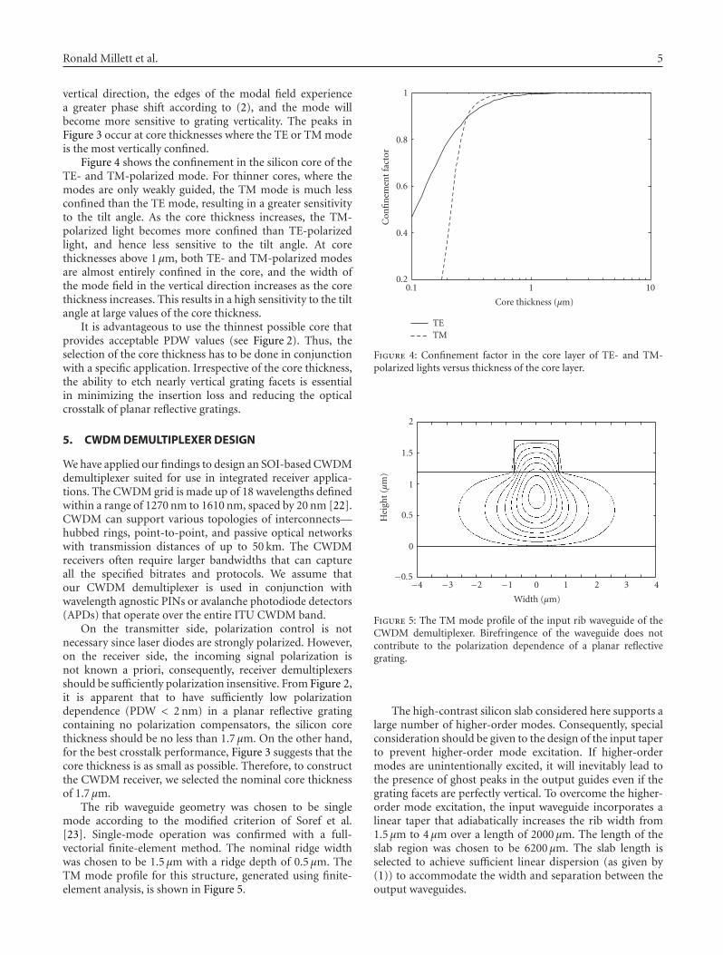
Figure 4 shows the confinement in the silicon core of theTE- and TM-polarized mode. For thinner cores, where themodes are only weakly guided, the TM mode is much lessconfined than the TE mode, resulting in a greater sensitivityto the tilt angle. As the core thickness increases, the TM-polarized light becomes more confined than TE-polarizedlight, and hence less sensitive to the tilt angle. At corethicknesses above 1 μm, both TE- and TM-polarized modesare almost entirely confined in the core, and the width ofthe mode field in the vertical direction increases as the corethickness increases. This results in a high sensitivity to the tiltangle at large values of the core thickness.
It is advantageous to use the thinnest possible core thatprovides acceptable PDW values (see Figure 2). Thus, theselection of the core thickness has to be done in conjunctionwith a specific application. Irrespective of the core thickness,the ability to etch nearly vertical grating facets is essentialin minimizing the insertion loss and reducing the opticalcrosstalk of planar reflective gratings.
5. CWDM DEMULTIPLEXER DESIGN
We have applied our findings to design an SOI-based CWDMdemultiplexer suited for use in integrated receiver applica-tions. The CWDM grid is made up of 18 wavelengths definedwithin a range of 1270 nm to 1610 nm, spaced by 20 nm [22].CWDM can support various topologies of interconnects—hubbed rings, point-to-point, and passive optical networkswith transmission distances of up to 50 km. The CWDMreceivers often require larger bandwidths that can captureall the specified bitrates and protocols. We assume thatour CWDM demultiplexer is used in conjunction withwavelength agnostic PINs or avalanche photodiode detectors(APDs) that operate over the entire ITU CWDM band.
On the transmitter side, polarization control is notnecessary since laser diodes are strongly polarized. However,on the receiver side, the incoming signal polarization isnot known a priori, consequently, receiver demultiplexersshould be sufficiently polarization insensitive. From Figure 2,it is apparent that to have sufficiently low polarizationdependence (PDW < 2 nm) in a planar reflective gratingcontaining no polarization compensators, the silicon corethickness should be no less than 1.7 μm. On the other hand,for the best crosstalk performance, Figure 3 suggests that thecore thickness is as small as possible. Therefore, to constructthe CWDM receiver, we selected the nominal core thicknessof 1.7 μm.
The rib waveguide geometry was chosen to be singlemode according to the modified criterion of Soref et al.[23]. Single-mode operation was confirmed with a full-vectorial finite-element method. The nominal ridge widthwas chosen to be 1.5 μm with a ridge depth of 0.5 μm. TheTM mode profile for this structure, generated using finite-element analysis, is shown in Figure 5.
0.1 1 10
Core thickness (μm)
0.2
0.4
0.6
0.8
1
Con
fin
emen
tfa
ctor
TETM
Figure 4: Confinement factor in the core layer of TE- and TM-polarized lights versus thickness of the core layer.
−4 −3 −2 −1 0 1 2 3 4
Width (μm)
−0.5
0
0.5
1
1.5
2
Hei
ght
(μm
)
Figure 5: The TM mode profile of the input rib waveguide of theCWDM demultiplexer. Birefringence of the waveguide does notcontribute to the polarization dependence of a planar reflectivegrating.
The high-contrast silicon slab considered here supports alarge number of higher-order modes. Consequently, specialconsideration should be given to the design of the input taperto prevent higher-order mode excitation. If higher-ordermodes are unintentionally excited, it will inevitably lead tothe presence of ghost peaks in the output guides even if thegrating facets are perfectly vertical. To overcome the higher-order mode excitation, the input waveguide incorporates alinear taper that adiabatically increases the rib width from1.5 μm to 4 μm over a length of 2000 μm. The length of theslab region was chosen to be 6200 μm. The slab length isselected to achieve sufficient linear dispersion (as given by(1)) to accommodate the width and separation between theoutput waveguides.

6 Advances in Optical Technologies
The selection of the diffraction grating order is dictatedby the requirements imposed by the free spectral range (FSR)of the device. In general, the overlap between different ordersis determined by
(N + 1)λ1 = Nλ2. (4)
In order to accommodate all 18 channels spaced at 20 nm, asrequired for a CWDM receiver, Δλ = λ2− λ1 should be morethan 400 nm. Such a wide-free spectral range demands thediffraction order to be N = 1, yielding a free spectral range ofover 600 nm. While low-diffraction order devices are easilyachievable using the planar reflective grating technology,realizing such wide-free spectral range device using the AWGarchitecture would require an impractically large phase arrayregion that would have severe crosstalk limitations in SOI.
The Rowland circle configuration was chosen as a zero-order approximation to the position of refractive elementsand the plane of the input and output waveguides. The first-order correction was obtained through the use of standarddouble-astigmatic point improvement to the position ofthe grating facets [11]. In our case, we chose 1270 nmand 1610 nm as astigmatic wavelengths to compensate forthe reduced diffraction efficiency in the end channels. Theenergy of light diffracted by the grating was optimized byselecting a blaze wavelength of 1440 nm.
Careful consideration should be given to the selection ofdiffraction angles for the planar grating in SOI. Traditionally,planar reflective gratings in SOI have been selected tohave incident and reflected angles of around 40 degrees[4, 6]. However, building a wide-free spectral range CWDMdemultiplexer at such large diffracting angles would lead tosuboptimally shaped grating facets that are susceptible tocorner rounding and polarization dependence. While it ispossible to remove reflective material from the nonreflectivefacets to improve the grating efficiency, this would requireadditional postprocessing steps such as selective metal etchremoval.
The reduction in the planar grating diffraction efficiencydue to corner rounding is approximately equal to the ratiobetween the size of the round corner and the size ofthe reflective portion of the facet. It is advantageous tohave the size of the reflective facet much larger comparedto the corner rounding. Furthermore, the ratio of thereflective to nonreflective facet has been shown to be thekey for overcoming PDL in planar reflective gratings [24].Consequently, the diffraction angle should be low enoughto produce sufficiently wide reflecting facets for ease ofmanufacturing, while keeping the size of the nonreflectingfacets small enough to eliminate corner rounding andpolarization effects.
Our analysis of the grating parameters yielded a value of3.5 degrees for the angle of diffraction. At this diffractionangle, an average size of the reflective facet is 3 μm whilethe nonreflecting sidewall is only 0.2 μm. This results in theaspect ratio of the reflecting to nonreflecting facet of 15 :1, putting a limit of −0.3 dB on the maximum diffractionefficiency loss due to corner rounding. The total numberof facets was chosen to be 600. This ensured that well over
1.25 1.3 1.35 1.4 1.45 1.5 1.55 1.6
Wavelength (μm)
−40
−30
−20
−10
0
Tran
smis
sion
(dB
)
Figure 6: Transmission spectra of an 18-channel CWDM demulti-plexer for TM polarization. No decrease in the diffraction efficiencywas observed for the end channels. Optical crosstalk of better than−35 dB was achieved.
99% of the light from the input waveguide is capturedby the grating. Each grating facet was chosen to be anelliptical shape to further reduce aberration effects. Detailsof aberration reduction are described in [10].
To achieve a box-like channel profile for the CWDMdemultiplexer, the output waveguides are formed using a1.7-μm-deep etch with a waveguide width of 8 μm anda separation between waveguides of approximately 4 μm(see Figure 1). This output waveguide structure can supporta large number of modes. Since the proposed device isspecifically designed for use in receiver applications, weassume that the active area of the photodetector is sufficientlylarge to absorb all of the light in the multimode guide.
To simulate the grating performance, we used a full-vectorial finite-element method to compute the modes ofinput and output guides. An asymptotic approximation forHankel functions of large argument was then used to obtainthe intensity on the grating facets. This approximation wasused once again to obtain the reflected field Θ(λ) on theplane of the output waveguide structures. The demultiplexertransmission intensity at a specific wavelength was obtainedby a convolution of the diffracted light with the intensityprofile of each individual mode ϕi(λ) in each outputmultimode output waveguide:
T(λ) =∑i
⟨Θ(λ) | φi(λ)
⟩. (5)
The results of our simulation are shown in Figure 6 forTM polarization. It is worth pointing out that the diffractionefficiency at the end channels is as strong as the efficiency ofthe central channels. This was possible by our selection of theblaze wavelength of the planar grating to be in the middle ofthe free spectral range, and the use of the end wavelengthsfor astigmatic points. Crosstalk values of better than −35 dBhave been computed for all 18 channels. The 0.5-dB spectralwidth of an individual channel was estimated to be 16 nm.Considering that this device has a projected PDW of 2 nmdue to the slab birefringence, centering the wavelengthbetween the two extreme polarizations can potentially yield

Ronald Millett et al. 7
15 nm of useful bandwidth for each individual channel.Such wide spectral passbands can be useful for transmittinglarge-bandwidth data while still allowing for the temperaturedrift of the demultiplexer and the transmitter laser diodes.This work confirms that planar reflective gratings in SOIcan be used to achieve both wide-free spectral range andpolarization-insensitive performance.
Multiplexing and demultiplexing light is only one ofmany possible applications of planar reflective gratings insilicon interconnects. Planar reflective gratings can also beused in add-drop filters, repeaters, dispersion compensators,and gain equalizers. Because of their reflective nature,planar gratings can be very effective in stabilizing lasersources through wavelength locking. Additional applicationsof planar gratings will likely be found in optical clockingthrough the use of time domain to frequency domaininterferometry in silicon interconnects.
6. SUMMARY
In summary, we have investigated the optical properties ofplanar reflective gratings for building optical interconnectsin silicon on insulator for various silicon core thicknesses. Wehave shown that the dispersion of the slab can be controlledthrough the core thickness selection to produce polarization-insensitive gratings. The verticality of the grating facets hasbeen found to be the main contributing factor to the cumula-tive crosstalk in thick silicon cores. Our findings were appliedtowards the design and simulation of an 18-channel coarsewavelength division demultiplexer that has both a wide-free spectral range and polarization-insensitive performance.These results demonstrate that planar reflective gratingscan become an essential element in building many siliconphotonics applications.
REFERENCES
[1] A. W. Fang, H. Park, O. Cohen, R. Jones, M. J. Paniccia, andJ. E. Bowers, “Electrically pumped hybrid AlGaInAs-siliconevanescent laser,” Optics Express, vol. 14, no. 20, pp. 9203–9210, 2006.
[2] H. Park, A. W. Fang, R. Jones, et al., “A hybrid siliconevanescent photodetector,” in Proceedings of the 65th AnnualDevice Research Conference (DRC ’07), pp. 185–186, SouthBend, Ind, USA, June 2007.
[3] W. Bogaerts, P. Dumon, D. Van Thourhout, et al., “Compactwavelength-selective functions in silicon-on-insulator pho-tonic wires,” IEEE Journal on Selected Topics in QuantumElectronics, vol. 12, no. 6, pp. 1394–1401, 2006.
[4] J. Brouckaert, W. Bogaerts, P. Dumon, D. Van Thourhout,and R. Baets, “Planar concave grating demultiplexer fabricatedon a nanophotonic silicon-on-insulator platform,” Journal ofLightwave Technology, vol. 25, no. 5, pp. 1269–1275, 2007.
[5] S. Bidnyk, D. Feng, A. Balakrishnan, et al., “Silicon-on-insulator-based planar circuit for passive optical networkapplications,” IEEE Photonics Technology Letters, vol. 18, no.22, pp. 2392–2394, 2006.
[6] W. Wang, Y. Tang, Y. Wang, et al., “Etched-diffraction-grating-based planar waveguide demultiplexer on silicon-on-insulator,” Optical and Quantum Electronics, vol. 36, no. 6, pp.559–566, 2004.
[7] S. Bidnyk, A. Balakrishnan, A. Delage, et al., “Novel archi-tecture for design of planar lightwave interleavers,” Journal ofLightwave Technology, vol. 23, no. 3, pp. 1435–1440, 2005.
[8] J. Brouckaert, W. Bogaerts, P. Dumon, et al., “Planar concavegrating demultiplexer with distributed bragg reflection facets,”in Proceedings of the 4th IEEE International Conference onGroup IV Photonics, pp. 1–3, Tokyo, Japan, September 2007.
[9] H. W. Yen, H. R. Friedrich, R. J. Morrison, and G. L. Tangonan,“Planar Rowland spectrometer for fiber-optic wavelengthdemultiplexing,” Optics Letters, vol. 6, no. 12, pp. 639–641,1981.
[10] S. Bidnyk, A. Balakrishnan, A. Delage, et al., “Planar comb fil-ters based on aberration-free elliptical grating facets,” Journalof Lightwave Technology, vol. 23, no. 3, pp. 1239–1243, 2005.
[11] P. Cheben, “Wavelength dispersive planar waveguide devices:echelle gratings and arrayed waveguide gratings,” in OpticalWaveguides: From Theory to Applied Technologies, M. L. Calvoand V. Laksminarayanan, Eds., chapter 5, CRC Press, London,UK, 2007.
[12] S. Bidnyk, A. Balakrishnan, M. Pearson, M. Gao, and T.Hall, “Configurable coarse wavelength division demultiplexersbased on planar reflective gratings,” Optics Communications,vol. 262, no. 1, pp. 82–86, 2006.
[13] A. Delage and K. Dossou, “Polarisation dependent losscalculation in echelle gratings using finite element method andRayleigh expansion,” Optical and Quantum Electronics, vol. 36,no. 1–3, pp. 223–238, 2004.
[14] D.-X. Xu, P. Cheben, D. Dalacu, et al., “Eliminating thebirefringence in silicon-on-insulator ridge waveguides by useof cladding stress,” Optics Letters, vol. 29, no. 20, pp. 2384–2386, 2004.
[15] S. L. Chuang, Physics of Optoelectronic Devices, Wiley-Interscience, New York, NY, USA, 1995.
[16] J. J. He, E. S. Koteles, L. Erickson, B. Lamontagne, and A.Delage, “Optical grating-based device having a slab waveguidepolarization compensating region,” US patent 5937113, 1999.
[17] P. Cheben, D.-X. Xu, S. Janz, A. Delage, and D. Dalacu,“Birefringence compensation in silicon-on-insulator planarwaveguide demultiplexers using a buried oxide layer,” in Pho-tonics Packaging and Integration III, vol. 4997 of Proceedings ofSPIE, pp. 181–189, San Jose, Calif, USA, January 2003.
[18] P. Cheben, D.-X. Xu, S. Janz, and A. Delage, “Scaling downphotonic waveguide devices on the SOI platform,” in VLSICircuits and Systems, vol. 5117 of Proceedings of SPIE, pp. 147–156, Maspalomas, Spain, May 2003.
[19] W. Bogaerts, D. Taillaert, P. Dumon, E. Pluk, D. VanThourhout, and R. Baets, “A compact polarization-indepen-dent wavelength duplexer using a polarization-diversity SOIphotonic wire circuit,” in Proceedings of the Optical Fiber Com-munication and the National Fiber Optic Engineers Conference(OFC/NFOEC ’07), pp. 1–3, Anaheim, Calif, USA, March2007, paper OTuM2.
[20] D. K. Sparacin, S. J. Spector, and L. C. Kimerling, “Siliconwaveguide sidewall smoothing by wet chemical oxidation,”Journal of Lightwave Technology, vol. 23, no. 8, pp. 2455–2461,2005.
[21] J.-J. He, B. Lamontagne, A. Delage, L. Erickson, M. Davies,and E. S. Koteles, “Monolithic integrated wavelength demul-tiplexer based on a waveguide Rowland circle grating inInGaAsP/InP,” Journal of Lightwave Technology, vol. 16, no. 4,pp. 631–637, 1998.
[22] International Telecommunication Union, ITU-T Recommen-dation G.694.2, 2002.

8 Advances in Optical Technologies
[23] R. A. Soref, J. Schmidtchen, and K. Petermann, “Large single-mode RIB waveguides in GeSi-Si and Si-on-SiO2,” IEEEJournal of Quantum Electronics, vol. 27, no. 8, pp. 1971–1974,1991.
[24] S. Bidnyk, A. Balakrishnan, and M. Pearson, “Planar waveg-uide reflective diffraction grating,” US patent 7151635, 2006.

International Journal of
AerospaceEngineeringHindawi Publishing Corporationhttp://www.hindawi.com Volume 2010
RoboticsJournal of
Hindawi Publishing Corporationhttp://www.hindawi.com Volume 2014
Hindawi Publishing Corporationhttp://www.hindawi.com Volume 2014
Active and Passive Electronic Components
Control Scienceand Engineering
Journal of
Hindawi Publishing Corporationhttp://www.hindawi.com Volume 2014
International Journal of
RotatingMachinery
Hindawi Publishing Corporationhttp://www.hindawi.com Volume 2014
Hindawi Publishing Corporation http://www.hindawi.com
Journal ofEngineeringVolume 2014
Submit your manuscripts athttp://www.hindawi.com
VLSI Design
Hindawi Publishing Corporationhttp://www.hindawi.com Volume 2014
Hindawi Publishing Corporationhttp://www.hindawi.com Volume 2014
Shock and Vibration
Hindawi Publishing Corporationhttp://www.hindawi.com Volume 2014
Civil EngineeringAdvances in
Acoustics and VibrationAdvances in
Hindawi Publishing Corporationhttp://www.hindawi.com Volume 2014
Hindawi Publishing Corporationhttp://www.hindawi.com Volume 2014
Electrical and Computer Engineering
Journal of
Advances inOptoElectronics
Hindawi Publishing Corporation http://www.hindawi.com
Volume 2014
The Scientific World JournalHindawi Publishing Corporation http://www.hindawi.com Volume 2014
SensorsJournal of
Hindawi Publishing Corporationhttp://www.hindawi.com Volume 2014
Modelling & Simulation in EngineeringHindawi Publishing Corporation http://www.hindawi.com Volume 2014
Hindawi Publishing Corporationhttp://www.hindawi.com Volume 2014
Chemical EngineeringInternational Journal of Antennas and
Propagation
International Journal of
Hindawi Publishing Corporationhttp://www.hindawi.com Volume 2014
Hindawi Publishing Corporationhttp://www.hindawi.com Volume 2014
Navigation and Observation
International Journal of
Hindawi Publishing Corporationhttp://www.hindawi.com Volume 2014
DistributedSensor Networks
International Journal of