Embed Size (px)
Citation preview
Systems I: Computer Organization and Architecture
Lecture 10: Basic Computer Organization and Design
Instruction Codes
• An instruction code is a group of bits that instruct the computer to perform a specific operation.
• The operation code of an instruction is a group of bits that define operations such as addition, subtraction, shift, complement, etc.
• An instruction must also include one or more operands, which indicate the registers and/or memory addresses from which data is taken or to which data is deposited.
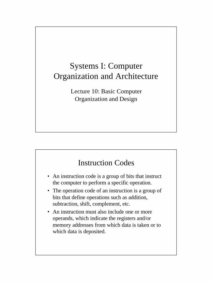
Microoperations
• The instructions are stored in computer memory in the same manner that data is stored.
• The control unit interprets these instructions and uses the operations code to determine the sequences of microoperations that must be performed to execute the instruction.
Stored Program Organization
• The operands are specified by indicating the registers and/or memory locations in which they are stored.– k bits can be used to specify which of 2k registers (or
memory locations) are to be used.• The simplest design is to have one processor register
(called the accumulator) and two fields in the instruction, one for the opcode and one for the operand.
• Any operation that does not need a memory operand frees the other bits to be used for other purposes, such as specifying different operations.
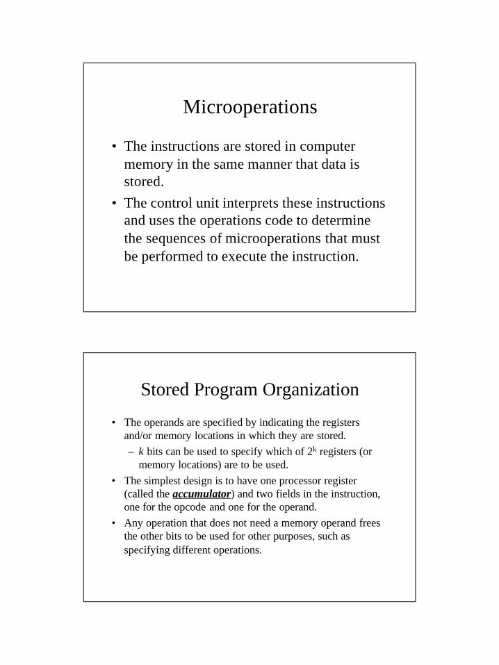
Stored Program Organization
Opcode Address
0111215
Instruction format
Binary operand
015
Memory4096 x 16
Instructions (programs)
Operands(data)
Processor Register(accumulator or AC)
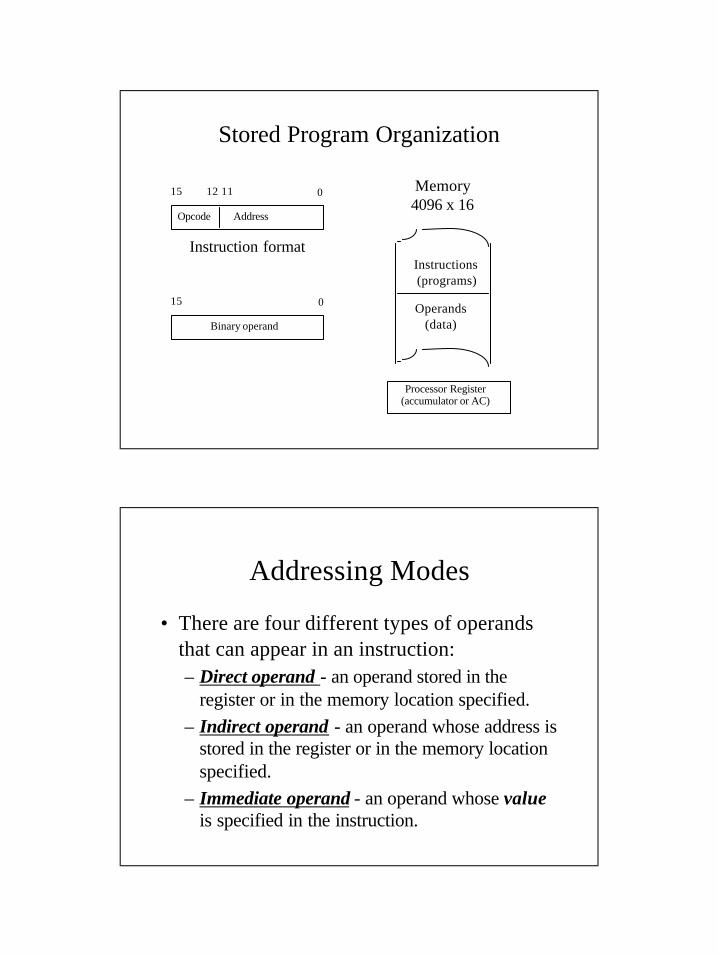
Addressing Modes
• There are four different types of operands that can appear in an instruction:– Direct operand - an operand stored in the
register or in the memory location specified.– Indirect operand - an operand whose address is
stored in the register or in the memory location specified.
– Immediate operand - an operand whose valueis specified in the instruction.
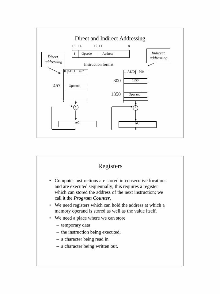
Direct and Indirect Addressing
Opcode Address
0111215
Instruction format
I
14
AC
Operand
0 ADD 457
+
AC
Operand
1 ADD 300
+
1350
457300
1350
IndirectaddressingDirect
addressing
Registers
• Computer instructions are stored in consecutive locations and are executed sequentially; this requires a register which can stored the address of the next instruction; we call it the Program Counter.
• We need registers which can hold the address at which a memory operand is stored as well as the value itself.
• We need a place where we can store– temporary data– the instruction being executed, – a character being read in – a character being written out.
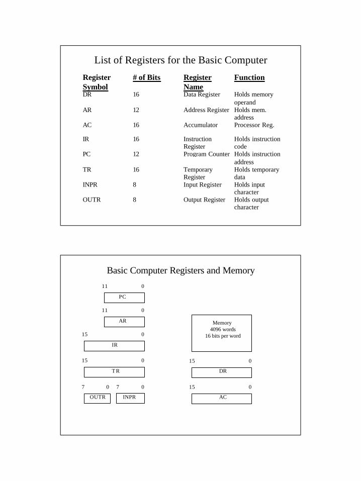
List of Registers for the Basic Computer
RegisterSymbol
# of Bits Register Name
Function
DR 16 Data Register Holds memoryoperand
AR 12 Address Register Holds mem.address
AC 16 Accumulator Processor Reg.
IR 16 InstructionRegister
Holds instructioncode
PC 12 Program Counter Holds instructionaddress
TR 16 TemporaryRegister
Holds temporarydata
INPR 8 Input Register Holds inputcharacter
OUTR 8 Output Register Holds outputcharacter
Basic Computer Registers and Memory
PC
011
AR
011
IR
015
T R
015
OUTR
07
INPR
0 7
DR
015
AC
015
Memory 4096 words
16 bits per word
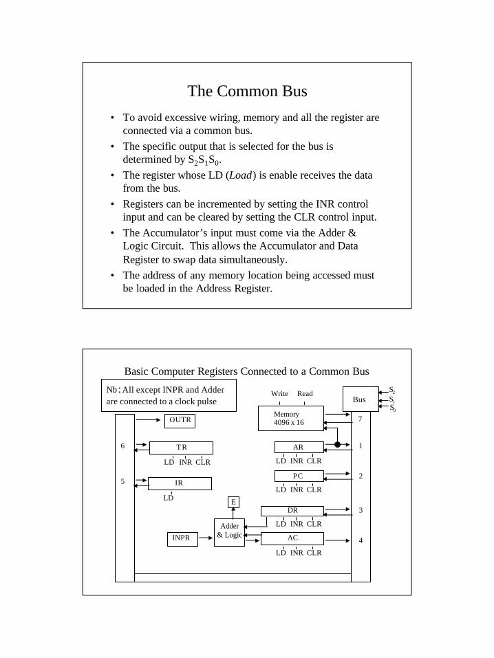
The Common Bus• To avoid excessive wiring, memory and all the register are
connected via a common bus.• The specific output that is selected for the bus is
determined by S2S1S0.• The register whose LD (Load) is enable receives the data
from the bus.• Registers can be incremented by setting the INR control
input and can be cleared by setting the CLR control input.• The Accumulator’s input must come via the Adder &
Logic Circuit. This allows the Accumulator and Data Register to swap data simultaneously.
• The address of any memory location being accessed must be loaded in the Address Register.
Basic Computer Registers Connected to a Common Bus
Bus
Memory4096 x 16
Write Read
AR
LD INR CLR
PC
LD INR CLR
DR
LD INR CLR
AC
LD INR CLR
Adder& Logic
E
INPR
IR
LD
T R
LD INR CLR
OUTR 7
1
2
3
4
6
5
S2
S1S0
Nb :All except INPR and Adder are connected to a clock pulse
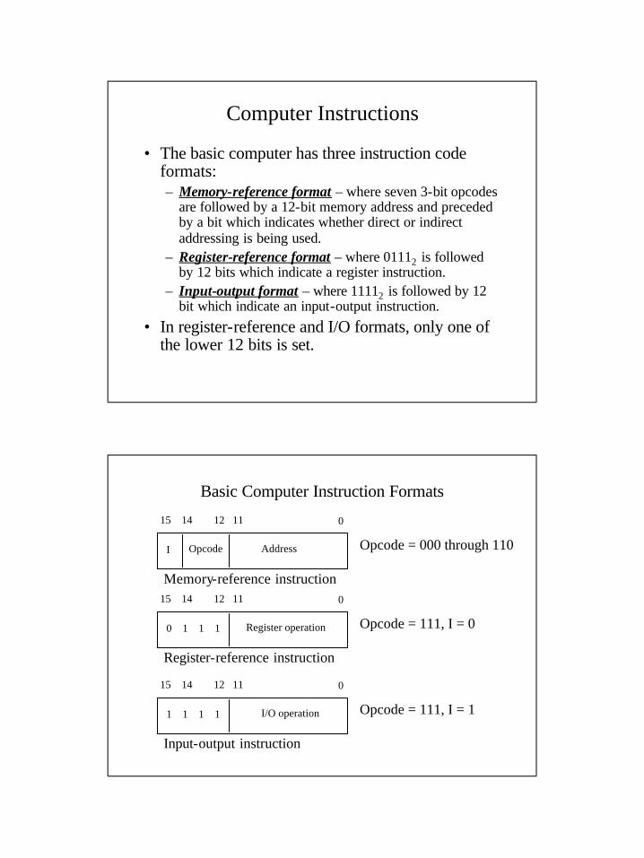
Computer Instructions
• The basic computer has three instruction code formats:– Memory-reference format – where seven 3-bit opcodes
are followed by a 12-bit memory address and preceded by a bit which indicates whether direct or indirect addressing is being used.
– Register-reference format – where 01112 is followed by 12 bits which indicate a register instruction.
– Input-output format – where 11112 is followed by 12 bit which indicate an input-output instruction.
• In register-reference and I/O formats, only one of the lower 12 bits is set.
Basic Computer Instruction Formats
011121415
I Opcode Address
Memory-reference instruction
Opcode = 000 through 110
011121415
0 1 1 1 Register operation
Register-reference instruction
Opcode = 111, I = 0
011121415
1 1 1 1 I/O operation
Input-output instruction
Opcode = 111, I = 1
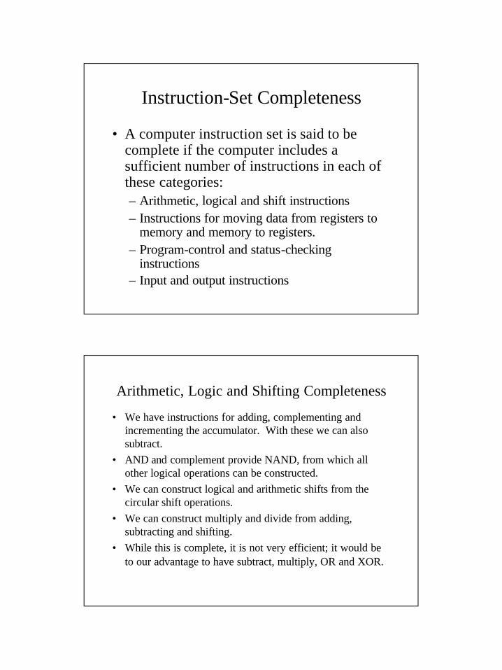
Instruction-Set Completeness
• A computer instruction set is said to be complete if the computer includes a sufficient number of instructions in each of these categories:– Arithmetic, logical and shift instructions– Instructions for moving data from registers to
memory and memory to registers.– Program-control and status-checking
instructions– Input and output instructions
Arithmetic, Logic and Shifting Completeness
• We have instructions for adding, complementing and incrementing the accumulator. With these we can also subtract.
• AND and complement provide NAND, from which all other logical operations can be constructed.
• We can construct logical and arithmetic shifts from the circular shift operations.
• We can construct multiply and divide from adding, subtracting and shifting.
• While this is complete, it is not very efficient; it would be to our advantage to have subtract, multiply, OR and XOR.
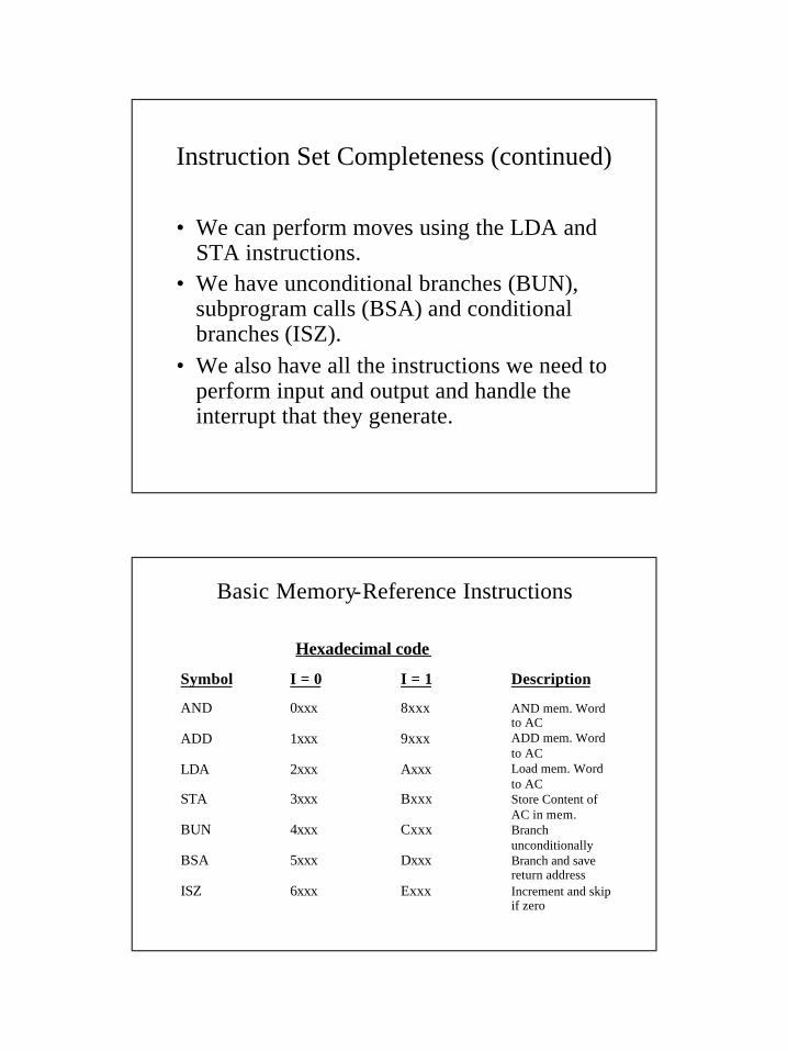
Instruction Set Completeness (continued)
• We can perform moves using the LDA and STA instructions.
• We have unconditional branches (BUN), subprogram calls (BSA) and conditional branches (ISZ).
• We also have all the instructions we need to perform input and output and handle the interrupt that they generate.
Basic Memory-Reference Instructions
Symbol I = 0 I = 1 Description
AND 0xxx 8xxx AND mem. Wordto AC
ADD 1xxx 9xxx ADD mem. Wordto AC
LDA 2xxx Axxx Load mem. Wordto AC
STA 3xxx Bxxx Store Content ofAC in mem.
BUN 4xxx Cxxx Branchunconditionally
BSA 5xxx Dxxx Branch and savereturn address
ISZ 6xxx Exxx Increment and skipif zero
Hexadecimal code
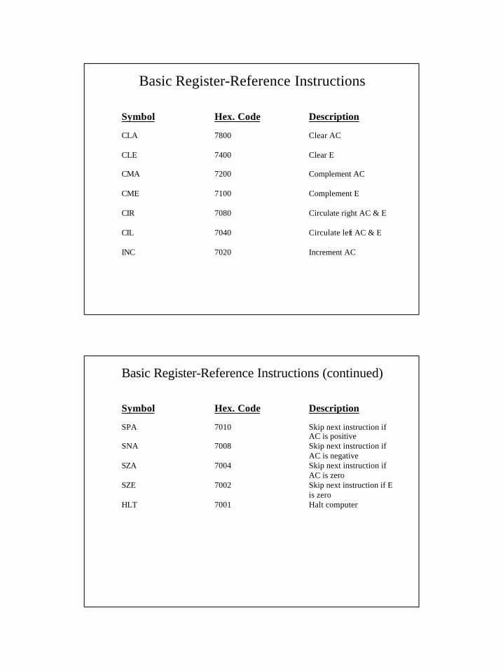
Basic Register-Reference Instructions
Symbol Hex. Code Description
CLA 7800 Clear AC
CLE 7400 Clear E
CMA 7200 Complement AC
CME 7100 Complement E
CIR 7080 Circulate right AC & E
CIL 7040 Circulate left AC & E
INC 7020 Increment AC
Basic Register-Reference Instructions (continued)
Symbol Hex. Code Description
SPA 7010 Skip next instruction ifAC is positive
SNA 7008 Skip next instruction ifAC is negative
SZA 7004 Skip next instruction ifAC is zero
SZE 7002 Skip next instruction if Eis zero
HLT 7001 Halt computer
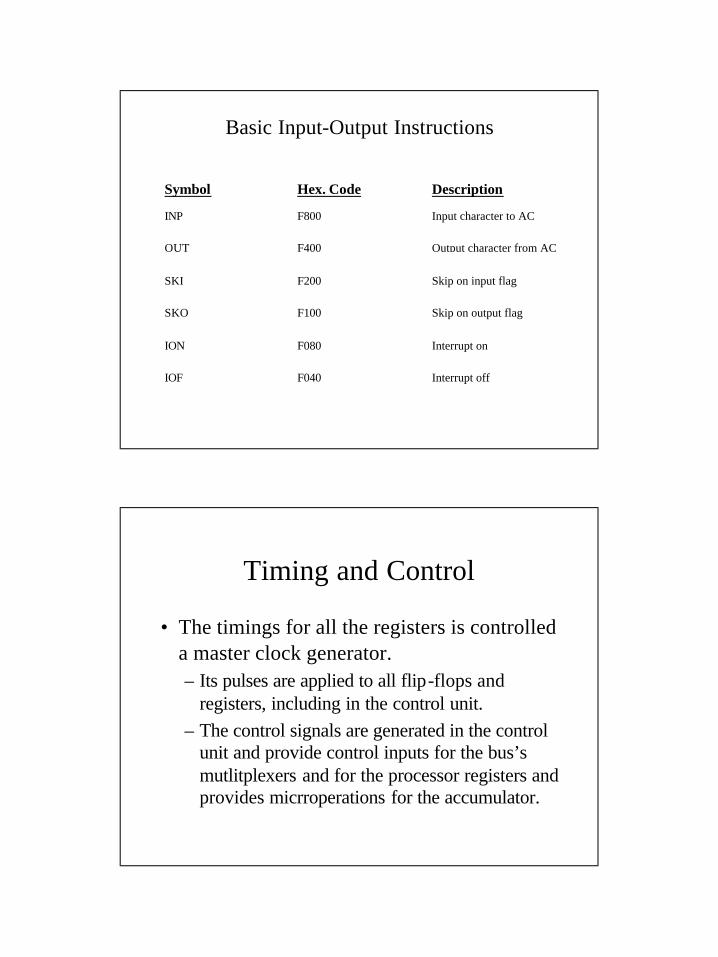
Basic Input-Output Instructions
Symbol Hex. Code Description
INP F800 Input character to AC
OUT F400 Output character from AC
SKI F200 Skip on input flag
SKO F100 Skip on output flag
ION F080 Interrupt on
IOF F040 Interrupt off
Timing and Control
• The timings for all the registers is controlled a master clock generator.– Its pulses are applied to all flip-flops and
registers, including in the control unit.– The control signals are generated in the control
unit and provide control inputs for the bus’s mutlitplexers and for the processor registers and provides micrroperations for the accumulator.
Control
• There are two types of control:– Hardwired – control logic is implemented with
gates, flip-flops, decoders and other digital circuits.
– Microprogrammed – control information is stored in a control program, which is programmed to perform the necessary steps to implement instructions.
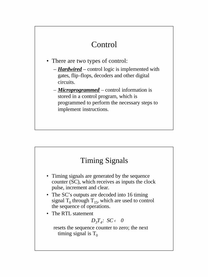
Timing Signals
• Timing signals are generated by the sequence counter (SC), which receives as inputs the clock pulse, increment and clear.
• The SC’s outputs are decoded into 16 timing signal T0 through T15, which are used to control the sequence of operations.
• The RTL statement D3T4: SC ← 0
resets the sequence counter to zero; the next timing signal is T0
Control Unit of Basic Computer
ControlLogicGates
Controloutputs
Other inputs
15 14 13 12 11 - 0
Instruction Register(IR)
3 x 8decoder
7 6 5 4 3 2 1 0D0
D7
15 0
T15
T0
4 x 16decoder
4-bitsequence counter
(SC)
Increment(INR)
Clear (CLR)
Clock
Examples of Control Timing Signals
ClockT0 T1 T2 T3 T4 T0
T0
T1
T2
T3
T4
D3
CLRSC
Instruction Cycle
• The instructions of a program are carried out by a process called the instruction cycle.
• The instruction cycle consists of these phases:– Fetch an instruction from memory– Decode the instruction– Read the effective address from memory if the
operand has an indirect address.– Execute the instruction.
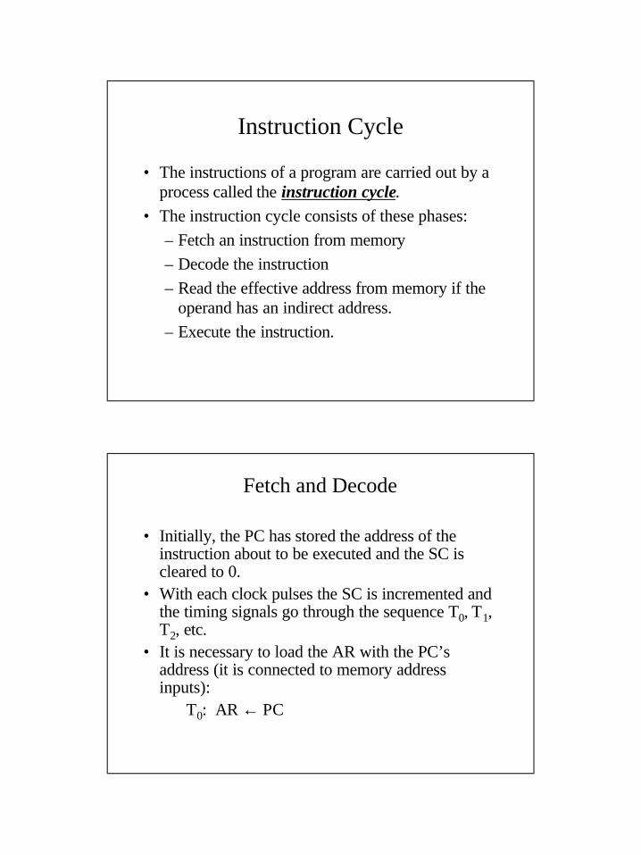
Fetch and Decode
• Initially, the PC has stored the address of the instruction about to be executed and the SC is cleared to 0.
• With each clock pulses the SC is incremented and the timing signals go through the sequence T0, T1, T2, etc.
• It is necessary to load the AR with the PC’s address (it is connected to memory address inputs):
T0: AR ← PC
Fetch and Decode
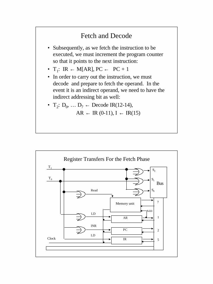
• Subsequently, as we fetch the instruction to be executed, we must increment the program counter so that it points to the next instruction:
• T1: IR ← M[AR], PC ← PC + 1• In order to carry out the instruction, we must
decode and prepare to fetch the operand. In the event it is an indirect operand, we need to have the indirect addressing bit as well:
• T2: D0, … D7 ← Decode IR(12-14), AR ← IR (0-11), I ← IR(15)
Register Transfers For the Fetch Phase
Bus
Memory unit 7
AR
Addr
1
Read
LD
PCINR
IRLD
T1
T0
2
5Clock
S2
S1
S0
Type of Instruction and Addressing
• During time T3, the control unit determines if this is a memory-reference, register-reference or input/output instruction.– The latter two are distinguished by the I (indirect) bit.– If it is a memory-reference instruction, the I bit will
determine direct or indirect addressing.• The four separate paths are:
D7’IT3: AR ← M[AR]D7’I’T3: NothingD7I’T3: Execute a register-reference instructionD7IT3: Execute an input-output instruction
Flowchart For Instruction CycleStart
SC ← 0
AR ← PC
T0
IR ←M[AR}, PC ← PC + 1
Decode opcode in IR(12-14)AR ←IR(0-11), I ← IR(15)
T1
T2
D7
(Register or I/O) = 1 = 0 (Memory-ref.)I I= 0 (reg.)
= 1 (I/O)
Exec. I/O inst.SC ← 0
Exec. reg.inst.SC ← 0
= 1
= 0 (Direct)
NothingAR ← M[AR]
Exec. memory ref. .inst.SC ← 0
T3T3T3
T3
Execution of Register-Reference Instructions
D7I’T3 = r (common to all register-reference instructions)IR(I) = Bi [bit in IR(0-11) that specifies the operation]
r SC ← 0 Clear SCC L A rB 11 A C ← 0 Clear ACC L E rB 10 E ← 0 Clear EC M A rB 9 A C ← AC ' Complement ACC M E rB 8 E ← E' Complement ECIR rB 7 A C ← shr AC,
AC(15) ← EE ← AC(0)
Circulate right
CIL rB 6 A C ← shl AC,AC(0) ← EE ← AC(15)
Circulate left
INC rB 5 A C ← AC + 1 Increment AC
Execution of Register-Reference Instructions
SPA rB4 If (AC(15) = 0)then PC ← PC + 1
Skip if positive
SNA rB3 If (AC(15) = 1)Then PC ← PC + 1
Skip if negative
SZA rB2 If (AC = 0)Then PC ← PC + 1
Skip if AC zero
SZE rB1 If (E = 0)Then PC ← PC + 1
Skip if E zero
HLT rB0 S ← 0 (S is a start-stopflip-flop)
Halt computer
Memory-Reference InstructionsSymbol Op. Decoder Symb. Desc.
AND D0 AC ← AC ∧ M[AR]
ADD D1 AC ← AC + M[AR], E ← Cout
LDA D2 AC ← M[AR]
STA D3 M[AR] ← AC
BUN D4 PC ← AR
BSA D5 M[AR] ← PC PC ← AR + 1
ISZ D6 M[AR] ← M[AR] + 1 If M[AR] + 1 = 0 Then PC ← PC + 1
Memory-Reference Instructions
• All memory-reference instructions have to wait until T4 so that the timing is the same whether the operand is direct or indirect.
• AND, ADD and LDA must all be performed in two steps because AC can only be access via DR:
• AND: D0T4: DR ← M[AR]D0T5: AC ← AC ∧ DR, SC ← 0
• ADD: D1T4: DR ← M[AR]D1T5: AC ← AC + DR, E ← Cout, SC ← 0
• LDA: D2T4: DR ← M[AR]D0T5: AC ← DR, SC ← 0
Memory-Reference Instructions (continued)
• STA stores the contents of the AC, which can be applied directly to the bus:D3T4: M[AR] ← AC, SC ← 0
• BUN transfers control unconditionally to th effective address indicated by the effective address:D4T4: PC ← AR, SC ← 0
• BSA is used to branch to a subprogram. This requires saving the return address, which is saved at the operand’s effective address with the subprogram beginning one word later in memory:
• D5T4: M[AR] ← PC, AR ← AR + 1D5T5: PC ← AR, SC ← 0
Example of BSA Instruction Execution
Memory, PC, & AR at time T4
Memory
20
PC= 21
AR = 135
136
0 BSA 135
1 BUN 135
Next instruction
Subroutine
Memory & PC after execution
Memory
20
21
135
PC = 136
0 BSA 135
1 BUN 135
Next instruction
Subroutine
21
Memory-Reference Instructions (continued)
• ISZ skips the next instruction if the operand stored at the effective address is 0. This requires that the PC incremented, which cannot be done directly:
• D6T4: DR ← M[AR]D6T5: DR ← DR + 1D6T6: M[AR] ← DR,
if (DR = 0) then (PC ← PC + 1),SC ← 0
Flowchart For Memory-Reference Instructions
Memory -reference Instructions
DR ← M[AR]
D0T 4
DR ← M[AR]
D1T 4
DR ← M[AR]
D2T 4
M[AR] ← ACSC ← 0
D3T 4
AC ← AC ∧ DRSC ← 0
D0T 5
AC ← AC + DRE ← C outSC ← 0
D1T 5
AC ← DRSC ← 0
D2T 5
ADDAND LDA STA
Flowchart For Memory-Reference Instructions (continued)
Memory -reference Instructions
PC ← ARSC ← 0
D4T 4
M[AR] ← PCAR ← AR + 1
D5T 4
DR ← M[AR]
D6T 4
M[AR] ← DRIF (DR = 0)then (PC ← PC+1)SC ← 0
D6T 6PC ← ARSC ← 0
D5T 5
BSABUN ISZ
DR ← DR + 1
D6T 5
Input-Output Configuration
Serial Comm.Interface
Input-outputterminal
Comp. Registersand Flip-flops
FGO
OUTR
AC
INPR
FGI
ReceiverInterface
Printer
TransmitterInterface
Keyboard
= 1 NOP= 0 output
data
= 0 NOP= 1 input
waiting
Input-Output Instructions
p SC ← 0 Clear SC
INP pB11 AC(0-7) ← INPR,FGI ← 0
Input character
OUT pB10 OUTR ← AC(0-7),FGO ← 0
Output character
SKI pB9 If (FGI = 1)Then PC ← PC + 1
Skip on input flag
SKO pB8 If (FGO = 1)Then PC ← PC + 1
Skip on output flag
ION pB7 IEN ← 1 Interrupt enable on
IOF pB6 IEN ← 0 Interrupt enable off
Flowchart For Interrupt Cycle
R
Fetch & decodeinstruction
Executeinstruction
= 0
Store return addressin location 0M[0] ← PC
Branch to location 1PC ← 1
IEN ← 0R ← 0
IEN
FGI
FGO
= 0
= 1
= 0
R ← 1
= 1
= 1
= 1Instruction cycle Interrupt cycle
= 0
Demonstration of the Interrupt Cycle
Before Interrupt
Memory
0
1
PC = 255
256
0 BUN 1120
1 BUN 0
I/OProgram
After Interrupt Cycle
Memory
0
PC = 1
255
0 BUN 1120
1 BUN 0
256
MainProgram
1120 I/OProgram
256
MainProgram
Flowchart For Computer OperationStart
SC← 0, IEN ← 0, R ← 0
R
AR ← 0, TR ← PCAR ← PC
RT0R’T0
M[AR] ←TR, PC ← 0
RT1
IR ← M[AR], PC ← PC + 1
R’T1
= 0 = 1
PC ← PC + 1, IEN ← 0R ← 0, SC ← 0
RT2
AR ← IR(0-11), I ← IR(15)D0…D7 ← Decode IR(12-14)
R’T2
D7
I
InstructionCycle
InterruptCycle
Execute I/OInstruction
Execute Reg.Instruction
= 0= 1 D7I’T3D7IT3 I
AR ← M[AR] Nothing
= 0= 1 D’7I’T3D’7IT3
Execute Mem..Instruction
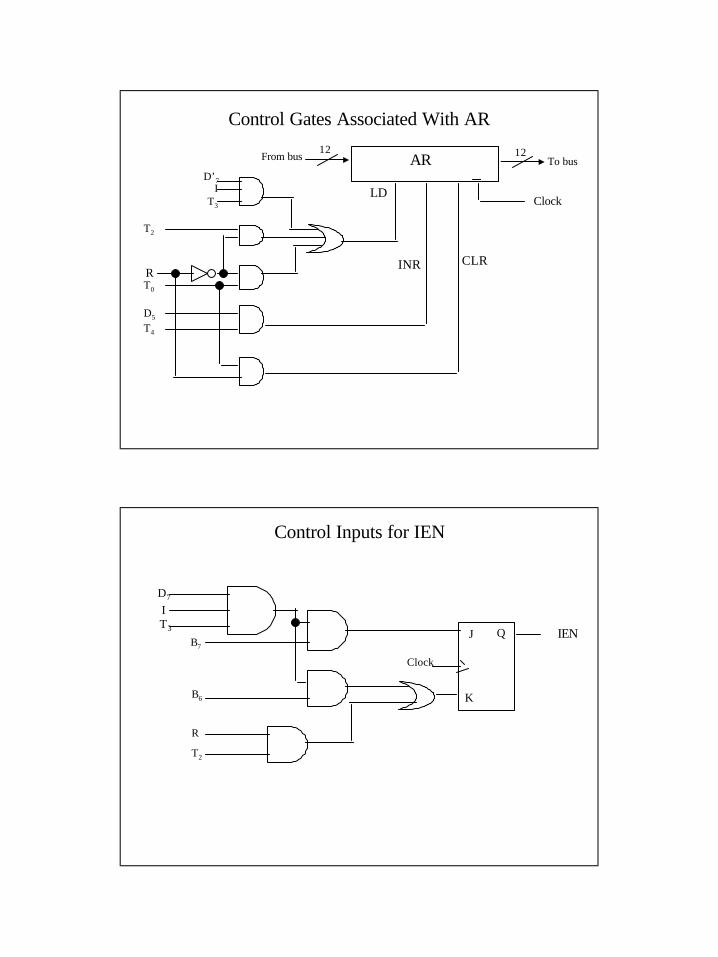
Control Gates Associated With AR
AR 12To bus
12From bus
Clock
D’7I
T3
T2
RT0
D5
T4
LD
INR CLR
Control Inputs for IEN
IENQJ
K
Clock
T3
ID7
B7
B6
R
T2
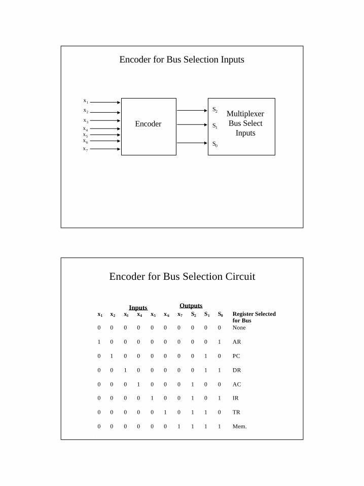
Encoder for Bus Selection Inputs
S1
S2
S0
MultiplexerBus Select
InputsEncoder
x1
x2
x3
x4x5x6
x7
Encoder for Bus Selection Circuit
x1 x2 x3 x4 x5 x 6 x7 S2 S1 S0 Register Selected for Bus
0 0 0 0 0 0 0 0 0 0 None
1 0 0 0 0 0 0 0 0 1 AR
0 1 0 0 0 0 0 0 1 0 PC
0 0 1 0 0 0 0 0 1 1 DR
0 0 0 1 0 0 0 1 0 0 AC
0 0 0 0 1 0 0 1 0 1 IR
0 0 0 0 0 1 0 1 1 0 TR
0 0 0 0 0 0 1 1 1 1 Mem. T R
Inputs Outputs
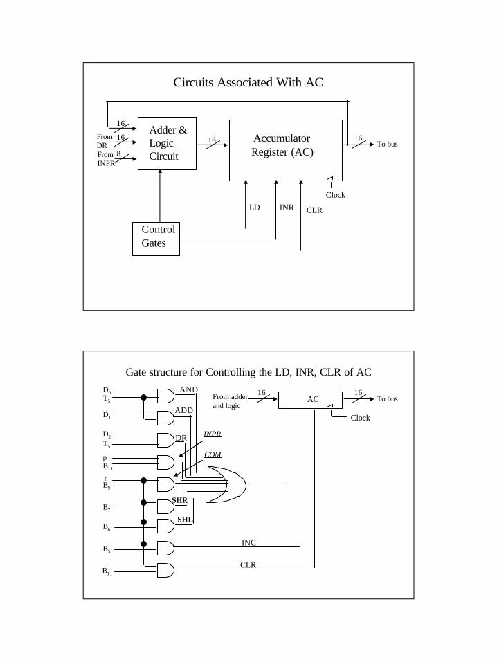
Circuits Associated With AC
16To bus16 Accumulator
Register (AC)
ControlGates
Clock
CLRINRLD
Adder &LogicCircuit
16
16
8
FromDRFromINPR
Gate structure for Controlling the LD, INR, CLR of AC
AC16
To bus
Clock
AND
ADD
DR INPR
COM
SHR
SHL
INC
CLR
rB9
B7
B6
B5
B11
D0T5
D1
D2
T5
pB11
16From adderand logic
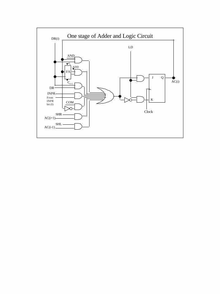
One stage of Adder and Logic Circuit
J
K
Q
Clock
AC(i)
FA
ci
Ci+1
DR(i)
DR
AND
ADD
INPRFromINPRbit (I)
COM
SHL
SHR
AC(i-1)
AC(i+1)
LD


![COMPUTER ORGANIZATION Subject Code: 10CS46 - VTU Solutionvtusolution.in/.../cse-iii-computer__organization_[15cs34]-notes.pdf · COMPUTER ORGANIZATION 10CS46 . COMPUTER ORGANIZATION](https://img.pdfslide.net/doc/110x75/5b7970717f8b9a331e8dcaf3/computer-organization-subject-code-10cs46-vtu-15cs34-notespdf-computer.jpg)