Embed Size (px)
Citation preview
TECHNISCHE UNIVERSITÄT DRESDEN
Fakultät für Maschinenwesen Institut für Werkstoffwissenschaft
DOKTORARBEIT
Study in analytical glow discharge spectrometry and
its application in materials science
zum Erlangen des akademischen Grades Doktoringenieur (Dr.-Ing.)
vorgelegt von Varvara Efimova
geboren am 07.12.1984


1. Gutachter: Prof. Dr. Jürgen Eckert
2. Gutachter: Prof. Dr. Arne Bengtson
Tag der Verteidigung: 18. August 2011
1
Content
Kurzfassung ........................................................................................................ 3
Abstract ............................................................................................................... 5
1 MOTIVATION AND DISSERTATION SCOPE .............................................. 8
2 INTRODUCTION ......................................................................................... 11
2.1 The Glow Discharge (GD) ......................................................................... 11
2.1.1 GD plasma......................................................................................... 11
2.1.2 GD sputtering vs. other sputtering techniques ................................... 15
2.1.3 GD sources........................................................................................ 16
2.2 Glow Discharge Optical Emission Spectrometry (GD OES) .................. 18
2.2.1 Basic principles of GD OES............................................................... 18
2.2.2 Quantification in GD OES .................................................................. 19
2.2.3 GD OES vs. other depth profiling methods ........................................ 23
2.3 Pulsed glow discharge (PGD)................................................................... 24
2.3.1 Virtues and shortcomings of the pulsed mode ................................... 24
2.3.2 Rf or dc pulsing?................................................................................ 26
2.3.3 How big is the thermal stress reduction when PGD is applied?......... 29
2.4 Measurement of the discharge gas temperature .................................... 31
2.4.1 What is the temperature of the GD gas?............................................ 31
2.4.2 Determination of the GD temperature from the rotational
spectra of the molecules............................................................................ 35
2.4.3 Determination of the GD temperature from the Doppler
width of spectral lines ................................................................................ 37
2.4.4 Laser-light scattering technique for the measurement
of the GD temperature ................................................................................ 37
2.5 Applications ............................................................................................... 38
2.5.1 CIGSe thin film solar cells.................................................................. 38
2.5.2 SAW devices ..................................................................................... 43
3 EXPERIMENTAL DETAILS ........................................................................ 46
3.1 Measurement of the electrical characteristics ........................................ 46
3.2 Measurement of the sputtered crater shapes ......................................... 47
Content
2
3.3 Light emission and spectra measurement...............................................48
3.4 GD OES depth profiling and quantification .............................................48
4 RESULTS AND DISCUSSION ....................................................................51
4.1 Study of pulsed glow discharge ...............................................................51
4.1.1 Defining the range of the PGD parameters ........................................51
4.1.2 Electrical properties of PGD ...............................................................56
4.1.2.1 Voltage-current plots of PGD......................................................................... 57
4.1.2.2 Voltage and current signal shapes within the pulse ...................................... 63
4.1.3 Measurements of the PGD gas temperature ......................................71
4.1.3.1 Voltage-current plots of the PGD as a thermometer for the GD gas............. 71
4.1.3.2 Determination of the GD temperature from the rotational spectra
of nitrogen species.................................................................................................... 75
4.1.4 Study of the sputtered crater formation in the PGD............................79
4.1.4.1 Investigation of the sputtering rates............................................................... 80
4.1.4.2 Investigation of the sputtered crater shapes.................................................. 84
4.1.4.3 Correlation of the observed crater formation effects with the
GD OES depth profiles ............................................................................................. 89
4.1.4.4 Sputter-induced surface topography formation ............................................. 93
4.1.5 Light emission and spectra of the PGD ..............................................99
4.1.6 Quantification of the GD OES depth profiles measured with PGD ...106
4.1.6.1 Matrix specific calibration – solar cell samples............................................ 108
4.1.6.2 Matrix independent calibration – SAW samples.......................................... 113
4.2 Application of PGD in GD OES analysis ................................................117
4.2.1 Layer stacks of CIGSe thin film solar cells .......................................117
4.2.1.1 Comparison of GD OES with other depth profiling techniques ................... 117
4.2.1.2 The role of an Al2O3 barrier layer in achieving high efficiency
solar cells on flexible steel substrates .................................................................... 120
4.2.1.3 Investigation of the growth procedure of the Cu(In,Ga)Se2-films ................ 122
4.2.1.4 Study of Zn incorporation into CuInS2 solar cell absorbers ......................... 124
4.2.2 Electrode metallizations of SAW devices .........................................126
4.2.2.1 The role of Al in high performance Cu-based SAW devices ....................... 126
5 CONCLUSIONS.........................................................................................130
Bibliography..................................................................................................... 134
Acknowledgements..........................................................................................147
3
Kurzfassung
Die optische Glimmentladungsspektroskopie (engl. Glow Discharge Optical Emission
Spectrometry - GD OES) hat sich als eine vielfältige und schnelle Methode für die
direkte Analyse von festen Materialien erwiesen. Die Anwendung von gepulsten
Glimmentladungen (GD) bietet eine Reihe von Vorteilen im Vergleich zu einer
kontinuierlichen Entladung und erweitert dadurch das analytische Potential der
Methode. Die praktische Anwendung von gepulsten GD erfordert jedoch ein tiefes
Verständnis der Prozesse, die in der Entladung und im elektrischen System
ablaufen. Der Einfluss der Puls- und Plasmaparameter auf die analytische Leistung
der gepulsten GD ist bislang noch nicht umfassend erforscht worden.
Die Zielstellung dieser Arbeit besteht in der Untersuchung der Eigenschaften
der gepulsten GD, welche von besonderer Bedeutung sowohl für das Verständnis
des Entladungsprozesses als auch für analytische Anwendungen ist. Die
Auswirkungen der Pulsparameter auf die gepulste GD wurde für den Gleichstrom-
(DC) und Hochfrequenz- (HF) Modus untersucht und verglichen. Die Reihenfolge der
Untersuchungen wurde in dieser Arbeit wie folgt gewählt: elektrische Parameter,
Sputterkraterformen, Sputterraten und Lichtemission. Die Form des Sputterkraters
korreliert stark mit der Pulsdauer, selbst wenn das Tastverhältnis konstant ist. Die
Pulsdauer beeinflusst nicht nur die Kraterform, sondern auch die Intensität der
Emissionslinien (bei konstantem Tastverhältnis). Darüber hinaus ist dieser Einfluss
unterschiedlich für Atome und Ionen. Dieses Verhalten wurde an mehreren
Emissionslinien (atomar bzw. ionisch) nachgewiesen.
Aus der Analyse der U-I-Kennlinien der gepulsten GD ergab sich, dass es zu
einer Erhitzung des Plasmas bei höherem Tastverhältnis kommt. Dieser Effekt wurde
zur Bestimmung der Plasma-Gastemperatur ausgenutzt. Die ermittelten
Temperaturen wurden mit einer andere Methode verglichen. Aus der Abschätzung
ergab sich, dass die Plasmatemperatur bei gepulsten GD um bis zu 100 K gesenkt
werden und durch die Pulsparameter genauer eingestellt werden kann.
Der Einfluss des Sputterns auf Cu(In,Ga)Se2 (CIGSe) Dünnschichten von
Solarzellen wurde erstmals beschrieben. REM-Untersuchungen an GD-gesputterten
CIGSe Schichten haben gezeigt, dass die Sputtereffekte durch die Variation der
Pulsparameter reduziert werden können.
Kurzfassung
4
Es konnte gezeigt werden, dass HF- und DC-Entladungen dieselben Effekte
aufweisen und sich nur geringfügig voneinander unterscheiden. Daraus kann
geschlussfolgert werden, dass DC- und HF-Entladungen in Bezug auf elektrische
Eigenschaften, Kraterformen, Lichtemission und Temperatur sehr ähnlich sind.
Die Quantifizierung der mit gepulsten GD gemessenen Tiefenprofile ergab
ferner, dass die Anwendung der Quantifizierungsmethoden für den kontinuierlichen
Modus unter den gegebenen Bedingungen zulässig ist. Die Tiefenprofile von
Solarzellen-Schichten sowie SAW-Metallisierungen wurden anhand gepulster GD
gemessen und quantifiziert. Die empfohlenen Quantifizierungsmethoden können mit
kommerziellen GD OES-Geräten durchgeführt werden.
Die Untersuchungen an gepulsten GD sind insbesondere relevant für GD
OES-Anwendungen im Bereich der Werkstoffwissenschaft. Während der
Zusammenarbeit mit dem Helmholtz-Zentrum Berlin für Materialien und Energie und
der Arbeitsgruppe von Dr. Thomas Gemming (IFW Dresden) konnten optimierte,
gepulste GD OES Messungen erfolgreich zur Untersuchung von Dünnschicht-
Solarzellen bzw. hochleistungsbeständigen SAW-Metallisierungen angewendet
werden. Für die Solarzellen haben GD OES und SIMS Messungen geholfen, die
Rolle der Al2O3-Barriere in CIGSe/Mo/Al2O3 Schichtstapeln auf flexiblem
Stahlsubstrat besser zu verstehen (Al2O3 soll die Diffusion der Fe-Atome in CIGSe
verhindern). Die gemeinsame Untersuchung getemperter CIGSe-Schichten mit
gepulster GD OES und in-situ Synchrotron-XRD ergab neue Erkenntnisse zum
Schichtwachstum. Der Diffusionskoeffizient von Zn in CuInS2 wurde erstmals aus GD
OES-Tiefenprofilen bestimmt. Im Fall der SAW-Metallisierungen konnte die GD OES
zur Bestimmung des geeignetsten Herstellungsverfahrens einen wichtigen Beitrag
leisten. Die gepulste GD OES hat neben anderen Untersuchungsmethoden wie
TEM-EDX, XPS und Lebensdauermessungen die Verbesserung der
Leistungsbeständigkeit von Cu-Metallisierungen durch geringen Al-Zusatz aufklären
können.
5
Abstract
Glow Discharge Optical Emission Spectrometry (GD OES) has proved to be a
versatile analytical technique for the direct analysis of solid samples. The application
of a pulsed power supply to the glow discharge (GD) has a number of advantages in
comparison with a continuous one and thereby broadens the analytical potential of
the GD. However, because the pulsed GD (PGD) is a relatively new operation mode,
the pulsing and plasma parameters as well as their influence on the analytical
performance of the GD are not yet comprehensively studied.
The aim of this dissertation consists in the investigation of the PGD features,
which are crucial for both understanding the discharge plasma processes and
analytical applications. The influence of the pulsing parameters on the PGD is
ascertained and compared for direct current (dc) and radio frequency (rf) discharges.
In the research attention is firstly paid on the electrical parameters of PGD, then on
the sputtered crater shapes, sputtering rates and finally on the light emission. It is
found that the sputtered crater shape is strongly affected by the duration of the
applied pulses even when the duty cycle is fixed. The pulse length influences the
intensity of the light emission as well (at constant duty cycle). Moreover this influence
is different for emission lines of atoms and ions in the plasma. This phenomenon can
be seen at the comparison of atomic and ionic lines of different elements.
The voltage–current plots of the PGD are found to indicate heating of the
discharge gas when operating at high duty cycles. Using this feature a new method
for the estimation of the discharge gas temperature from the voltage-current
characteristics of the PGD is developed. The calculated temperature values are
compared with another temperature measurement technique. Different temperature
estimation procedures have shown that the discharge gas temperature can be
reduced by around 100 K when PGD is applied. The temperature measurements
have also confirmed that the gas heating can be adjusted by variation of the pulsing
parameters.
The effect of sputtering on the Cu(In,Ga)Se2 (CIGSe) layer surface of the solar
cells is described for the first time. SEM investigations of the CIGSe layer of the solar
cells have shown that sputter induced effects can be reduced by variation of the
pulsing parameters.
Abstract
6
With regard to the question whether dc and rf pulsed discharges behave
similarly: nearly all phenomena found with dc discharges also appear in the rf case.
Hence it is concluded that the pulsed rf and dc discharges are very similar in terms of
the electrical properties, sputtered crater formation, light emission and temperature.
It is concluded that matrix specific, as well as matrix independent
quantification principles and the intensity correction developed by Arne Bengtson can
be applied for the pulsed mode, if special conditions are fulfilled. CIGSe solar cell
samples and thin layered electrode metallizations of SAW devices are measured and
quantified with application of PGD. The proposed quantification procedures are
performed at commercial GD OES devices and can be used for the analysis with
application of pulsed rf discharge.
The studies of the PGD performed in this dissertation are relevant for the
application of the GD OES analysis in materials science. During the collaborative
work with Helmholtz-Zentrum Berlin für Materialien und Energie and with the
research group of Dr. Thomas Gemming at IFW Dresden the optimized pulsed GD
OES measurements could be successfully applied at the investigation of thin film
solar cells with CIGSe light absorbing layer and electrode matallizations of SAW
devices. In case of solar cell samples pulsed GD OES depth profiling along with
SIMS measurements reveal the role of the Al2O3 barrier layer in high efficiency solar
cells consisting of a CIGSe/Mo/Al2O3/steel substrate layer stack (the barrier layer is
to prevent the Fe diffusion into the CIGSe). The features of the CIGSe films growth
are studied with help of pulsed GD OES and in situ synchrotron XRD measurements.
The diffusion coefficient of Zn into the CuInS2 layer is determined for the first time
from the measured GD OES depth profiles of the corresponding solar cell samples.
In case of SAW samples, pulsed GD OES measurements helped to evaluate the
different SAW electrode preparation procedures and to select the most suitable one.
In addition pulsed GD OES depth profiling along with XPS, TEM-EDX and electrode
lifetime measurements indicate the possible mechanism of power durability and
lifetime improvement of the SAW devices when a small amount of Al is added to the
Cu-based electrodes.

7
8
1 Motivation and dissertation scope
Glow Discharge Optical Emission Spectrometry (GD OES) has proved to be a
versatile analytical technique for the direct analysis of solid samples. The mild but at
the same time fast sputtering glow discharge (GD) plasma lends itself to a wide
range of analytical applications, including the analysis of bulk metals and alloys, non-
conductive samples as well as depth-resolved analyses. The application of pulsed
voltage to ignite and sustain the GD plasma broadens the analytical potential of the
GD. Pulsed Glow Discharge (PGD) has some attractive features, as compared to the
continuous discharge, in particular: (1) with additional discharge parameters (duty
cycle, frequency and pulse duration) the sample removal rate can be controlled with
greater precision; (2) due to the transient power there are fewer problems with
overheating of the sputtered sample; (3) by recording of the emission at a certain
time of the pulse one can either suppress or intensify the signal of plasma species.
Although the PGD offers a number of advantages, its use in commercial
spectrometers has some limitations. Firstly, on the one hand, additional control
parameters give bigger room for the sputtering control, but on the other hand, more
parameters complicate the analysis. To find proper measurement conditions one
should study the influence of all discharge parameters on the analytical discharge
performance (depth resolution, light emission, quantification). As the PGD is a
relatively new technique, the parameters of the PGD are not yet comprehensively
investigated. Secondly, it is difficult to quantify the profiles measured with PGD,
because the existing quantification model is established for the continuous discharge.
Therefore, PGD is applied with modern commercial devices mostly for qualitative
analysis.
Motivation and dissertation scope
9
Besides the limitations of the PGD use in the commercial scale there are two
more fundamental aspects of the PGD which are until now not clarified: (1) It is well
known that one of the outstanding possibilities of PGD is the reduction of thermal
stress caused by sputtering. However, the extent of thermal stress reduction when
pulses are applied is not often discussed and measured. Also the influence of the
pulsing parameters (duty cycle, pulse duration and frequency) on the discharge gas
and sample temperature is not known. (2) The ability of insulator sputtering is a well
known difference between radio frequency (rf) and direct current (dc) discharges and
widely applied for the analysis. The detailed comparison of dc and rf discharges is
still a topic for debates. Some researchers suppose that ionisation and sputtering
efficiencies are different in dc and rf modes, and others believe that both modes are
similar.
Based on the above mentioned problems and questions regarding the PGD,
which complicate and restrict its application in analytics, the goals of the present
dissertation are formulated as follows:
• As one of the keys to understand the glow discharge is its electrical behaviour, the
first task of the present work is to study the influence of the PGD parameters (pulse
duration, pulse frequency and duty cycle) on the voltage–current characteristics and
current and voltage signal shapes within the pulse.
• The next objective of the work is to reveal the influence of the pulsing parameters
on the shape and roughness of the sputtered crater as well as on the sputtering rate.
The correlation between the electrical parameters and the sputtered crater formation
should be taken into account.
• The influence of the pulsing parameters on the spectra of both pulsed dc and rf
discharges is to be investigated in present work. The correlation of electrical
parameters with light emission effects should be taken into account.
• The important tasks of the work are to estimate the reduction of the GD gas
temperature at the application of pulsed discharge and to ascertain the impact of the
pulsing parameters on the discharge gas heating.
• To answer the question whether dc and rf pulsed discharges behave similarly all
experiments concerning the electrical properties, sputtered crater formation, light
emission and discharge gas temperature are to be performed for both modes.
Motivation and dissertation scope
10
• It is worthwhile to find an approach to quantify the depth profiles measured with
PGD. First of all it should be examined whether the existing quantification principles,
which are established for continuous discharge, are valid also for the pulsed mode.
• The studies of the PGD to be done in the course of the work are relevant for the
application of the GD analysis in materials science. To demonstrate this, two types of
layered materials analyzed by means of pulsed GD OES will be considered: thin film
solar cells with Cu(In,Ga)Se2 light absorbing layer and electrode metallizations of
Surface Acoustic Wave (SAW) devices.
The dissertation is divided into five main parts: (1) Motivation and dissertation scope,
(2) Introduction, (3) Experimental details, (4) Results and discussion and (5)
Conclusions.
In the “Introduction” the fundamentals, as well as virtues and shortcomings of
the glow discharge and GD OES analysis are introduced. The statement of the
dissertation tasks is argued by the actual data known from the literature. With regard
to the thin film solar cells and SAW devices, the state of the art as well as present
challenges in the scientific and industrial fields of these two layered systems are
shown. The importance of GD OES depth profiling with application of pulsed glow
discharge is discussed.
The part “Experimental details” includes the description of the special
equipment used for these studies, which is not introduced in the “Results and
discussion”.
The chapter “Results and discussion” deals with the main results of the work
and their interpretation. The study of electrical parameters of PGD, sputtered crater
formation, sputtering rates, light emission and quantification are consequently
described. Finally some examples are shown, where optimized pulsed GD OES
measurements are helpful at the investigation of thin film solar cells and SAW
devices.
The most outstanding results on the fulfilling of the above listed dissertation
goals are summarized in the “Conclusions”.
11
2 Introduction
2.1 The Glow Discharge (GD)
2.1.1 GD plasma
In 1705 the English scientist Francis Hauksbee demonstrated a partly evacuated
glass globe, which while charging by static electricity could produce a light bright
enough to read by. It was the first demonstration of the discharge phenomenon in
gas. In 1857 the German physicist and glassblower Heinrich Geissler invented the
first low pressure glow discharge (GD) source – an evacuated glass cylinder with an
electrode at each end, which was later called Geissler tube. Geissler tubes filled with
different discharge gases were mass produced as entertainment devices, with
various spherical chambers and decorative serpentine paths. The gas discharge
phenomenon played an important role also for the science. William Crookes, the
English chemist and physicist used the discharge tubes to study the properties of
cathode rays. Later on (in 1897) the British physicist and Nobel laureate Joseph John
Thomson identified the cathode rays as negatively-charged particles, later named
electrons. In 1852 William Robert Grove discovered the sputtering of cathode
material in a GD, which nowadays got a wide application area in industry and
analytics.
The Geissler tube is the classical device serving the study of the discharge
processes till nowadays. It consists of two metal electrodes immersed into a glass
tube with some gas, typically Ar. When the voltage between the electrodes is raised,
the current sharply increases at a certain voltage Ub and light emission appears.
These are the signs of a breakdown, where the insulating by nature gas becomes
Introduction
12
conductive because of the avalanche ionisation in the electric field. As a certain
portion of the particles in the gas is ionized, it is called plasma. According to the
Paschen’s law,1 Ub depends on the distance between the electrodes and the
pressure in the discharge cell. The type of discharge that forms after the breakdown
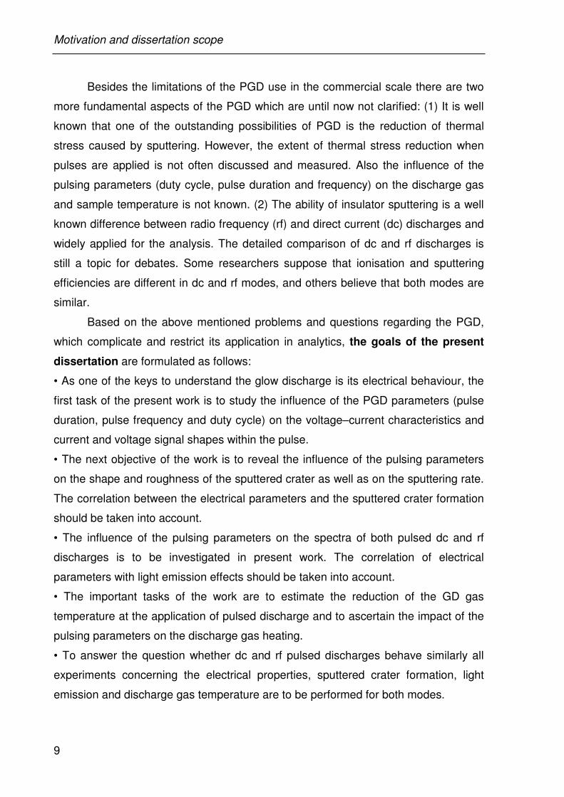
is defined by the applied voltage and current: Townsend discharge, normal GD,
abnormal GD or arc discharge (see Fig. 2-1). All these discharges are self-sustaining
because no external ionization agent, such as heating or X-ray radiation, is needed
to maintain them.
Fig. 2-1 Voltage-current characteristics of different self-sustaining gas discharges.
In Townsend discharge the voltage is equal to the ignition potential Ub and thus the
ionization degree is so small that the charge density (or current) has no influence on
the electric field. However at further current growth (for example at higher pressures)
the voltage across the electrodes begins to decrease and after a certain current the
fall stops indicating the normal glow discharge. The remarkable property of this mode
is that the current density doesn’t change. What is changed is the area through which
the current flows. When all the cathode area is exhausted the current density starts
to increase providing also a voltage increase. This discharge is said to be abnormal
and corresponds to the climbing area of the U-I curve in Fig. 2-1. When the discharge
current is high enough (around 1 A) an arc appears.2 For analytical purposes the
cathode is usually the sample itself. Hence the abnormal mode is most important,
Introduction
13
because the current density over the whole cathode area is the same what favors
homogeneous sputtering.
The GD develops under the following conditions: relatively low pressure of 1,3
- 13 hPa, low current of 10-6 – 10-1 A and a rather high voltage from hundreds to few
thousands of volts.2
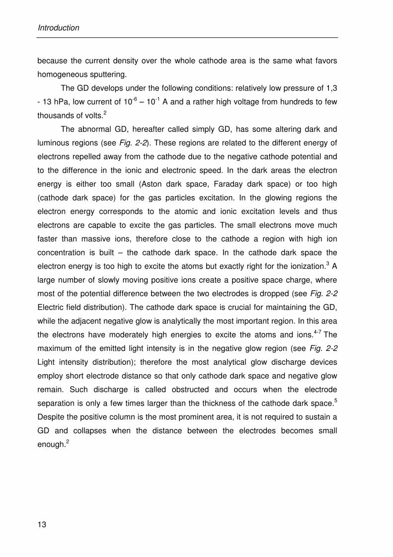
The abnormal GD, hereafter called simply GD, has some altering dark and
luminous regions (see Fig. 2-2). These regions are related to the different energy of
electrons repelled away from the cathode due to the negative cathode potential and
to the difference in the ionic and electronic speed. In the dark areas the electron
energy is either too small (Aston dark space, Faraday dark space) or too high
(cathode dark space) for the gas particles excitation. In the glowing regions the
electron energy corresponds to the atomic and ionic excitation levels and thus
electrons are capable to excite the gas particles. The small electrons move much
faster than massive ions, therefore close to the cathode a region with high ion
concentration is built – the cathode dark space. In the cathode dark space the
electron energy is too high to excite the atoms but exactly right for the ionization.3 A
large number of slowly moving positive ions create a positive space charge, where
most of the potential difference between the two electrodes is dropped (see Fig. 2-2
Electric field distribution). The cathode dark space is crucial for maintaining the GD,
while the adjacent negative glow is analytically the most important region. In this area
the electrons have moderately high energies to excite the atoms and ions.4-7 The
maximum of the emitted light intensity is in the negative glow region (see Fig. 2-2
Light intensity distribution); therefore the most analytical glow discharge devices
employ short electrode distance so that only cathode dark space and negative glow
remain. Such discharge is called obstructed and occurs when the electrode
separation is only a few times larger than the thickness of the cathode dark space.5
Despite the positive column is the most prominent area, it is not required to sustain a
GD and collapses when the distance between the electrodes becomes small
enough.2
Introduction
14
Fig. 2-2 Schematic picture and photo of the GD in tube as well as distribution of the electric field and glow intensity along the GD.
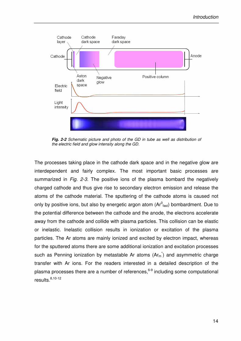
The processes taking place in the cathode dark space and in the negative glow are
interdependent and fairly complex. The most important basic processes are
summarized in Fig. 2-3. The positive ions of the plasma bombard the negatively
charged cathode and thus give rise to secondary electron emission and release the
atoms of the cathode material. The sputtering of the cathode atoms is caused not
only by positive ions, but also by energetic argon atom (Ar0fast) bombardment. Due to
the potential difference between the cathode and the anode, the electrons accelerate
away from the cathode and collide with plasma particles. This collision can be elastic
or inelastic. Inelastic collision results in ionization or excitation of the plasma
particles. The Ar atoms are mainly ionized and excited by electron impact, whereas
for the sputtered atoms there are some additional ionization and excitation processes
such as Penning ionization by metastable Ar atoms (Arm*) and asymmetric charge
transfer with Ar ions. For the readers interested in a detailed description of the
plasma processes there are a number of references,6-9 including some computational
results.8,10-12
Introduction
15
Fig. 2-3 Illustration of the most important basic processes that take place in an analytical GD plasma. Superscripts
0 and * denote the ground state and excited
states, respectively. Arm* symbolizes the Ar metastable atoms.
2.1.2 GD sputtering vs. other sputtering techniques
The ability to convert the solid samples directly into gaseous atoms and ions is a big
advantage for the analysis since a time consuming and laborious sample preparation
is avoided. The techniques which allow the direct analysis of solid samples are based
on ion bombardment, laser ablation and plasma-based processes.13,14 Ion beam
sputtering is used for depth profiling in SIMS, SNMS, XPS and AES. In these
methods a focused ion beam (ion energies in the keV region) is applied at high
vacuum conditions to sputter material from a specific location on a solid surface.15,16
Laser techniques are utilized in LIBS - the laser energy is transferred to the sample
surface resulting in the ejection of atoms and ions; the ablated sample material
generates a plasma and when local thermodynamic equilibrium is established, the
characteristic atomic emission lines of the elements can be observed.17 Moreover the
ablated material can be transferred to an ICP plasma and subsequently analyzed by
a mass spectrometer (LA-ICPMS).18 However the forming plasma is not reproducible;
therefore LIBS and LA-ICPMS suffer from poor precision. Among the plasma-based
techniques there are spark, arc and glow discharges. Sparks and arcs coupled to
Introduction
16
optical emission spectrometry are widely used for bulk analysis.14 Nevertheless the
erratic behavior renders them unable to depth profiling.
Sputtering in the GD is widely applied for both bulk and depth profile analysis
in GD OES and GD MS.19-22 GD sputtering has a greater number of attractive
features as compared to other sputtering techniques. Because of the relatively high
operational pressure (several hPa), atoms and ions in the GD undergo numerous
collisions transferring their kinetic energy and changing their trajectories (the mean
free path of the ions in the GD is around tens of µm).23 Hence in contrast to high
vacuum ion beam sputtering the atoms and ions in the GD strike the cathode with a
wide angular distribution.24,25 This favours homogeneous sputtering over the sample
surface, which in case of an ion beam can be reached only by sample rotation.26-28
Due to the frequent collisions the particles in the GD lose their energy and bombard
the cathode with significantly lower energies than at high vacuum sputtering (< 100
eV vs >1 keV).25,29-31 The trajectories of low energy ions in the bombarded material
are confined to a shallower depth. Also the number of collisions made by a projectile
in the solid is much smaller at low energies.32-34 The ejected atoms usually originate
from only few angstroms of the sample and have energies of 5 to 15 eV.35 Hence the
sputtering induced surface changes like ion implantation, atomic mixing and surface
topography formation36-40 are in case of GD less pronounced. As compared to high
vacuum sputtering, the GD has much greater current densities (100 mA/cm2 vs 1
µA/cm2) because of the higher pressure. Thus for GD sputtering the sample ablation
rates are much higher but with far less lattice damage.24
2.1.3 GD sources
The operation simplicity and the variety of analytical applications of GD led to the
development of several source configurations. The oldest one is the hollow
cathode.41 In this configuration a cylindrical hollow cathode is used so that the
negative glows from the opposite cylinder walls coalesce. Hence the current density,
the ionization and excitation efficiencies are much larger than the usual ones.42 The
hollow cathode source provides great sensitivity but its disadvantages are the
complicated sample geometry and exchange and the impossibility of depth profiling.
Another GD source configuration is the “pin-type” source, which is capable to sputter
Introduction
17
pin-shape samples or wires.43 This source is often used in mass spectrometry
because of the ion extraction simplicity and easy sample preparation. However,
depth profiling in the “pin-type” source is difficult.
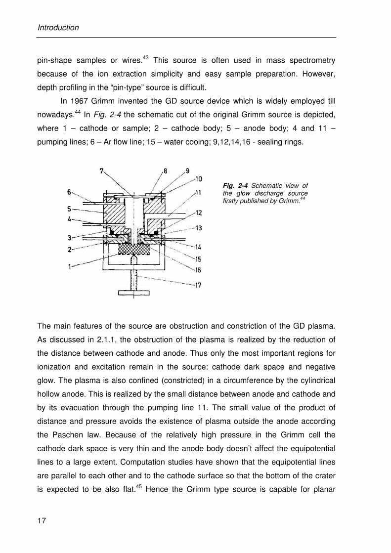
In 1967 Grimm invented the GD source device which is widely employed till
nowadays.44 In Fig. 2-4 the schematic cut of the original Grimm source is depicted,
where 1 – cathode or sample; 2 – cathode body; 5 – anode body; 4 and 11 –
pumping lines; 6 – Ar flow line; 15 – water cooing; 9,12,14,16 - sealing rings.
Fig. 2-4 Schematic view of the glow discharge source firstly published by Grimm.
44
The main features of the source are obstruction and constriction of the GD plasma.
As discussed in 2.1.1, the obstruction of the plasma is realized by the reduction of
the distance between cathode and anode. Thus only the most important regions for
ionization and excitation remain in the source: cathode dark space and negative
glow. The plasma is also confined (constricted) in a circumference by the cylindrical
hollow anode. This is realized by the small distance between anode and cathode and
by its evacuation through the pumping line 11. The small value of the product of
distance and pressure avoids the existence of plasma outside the anode according
the Paschen law. Because of the relatively high pressure in the Grimm cell the
cathode dark space is very thin and the anode body doesn’t affect the equipotential
lines to a large extent. Computation studies have shown that the equipotential lines
are parallel to each other and to the cathode surface so that the bottom of the crater
is expected to be also flat.45 Hence the Grimm type source is capable for planar
Introduction
18
sputtering of the sample at the proper discharge conditions46,47 and is well suited for
the depth profile analysis.48 In addition the Grimm geometry allows easy and fast
sample mounting.
For further improvement of the sputtered crater and thus of the depth
resolution, various attempts have been made to modify the basic Grimm source.49
For example a floating electrode50 or an auxiliary cathode51 were introduced between
cathode and anode. To increase the excitation efficiency boosted sources with
secondary discharge,52 magnetic field53 or additional gas flow towards the sample
surface54 have been designed. However the basic Grimm geometry is the most
abundant till nowadays.
2.2 Glow Discharge Optical Emission Spectrometry (GD OES)
2.2.1 Basic principles of GD OES
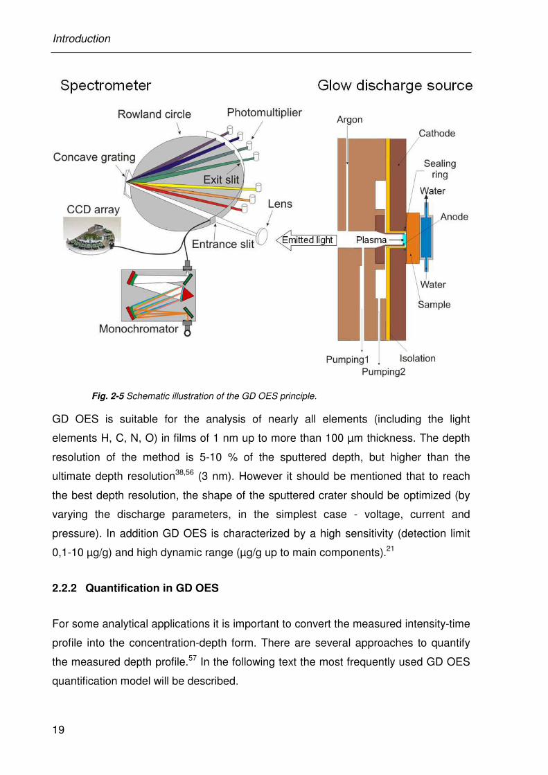
GD OES is known since 1967 when Grimm published the first results from his
analytical source.55 Starting from that time the interest in Grimm’s source in
combination with optical emission spectrometry has steadily grown. Nowadays GD
OES is employed for the analysis of steels and steel surfaces, other metallic coatings
and metals, PVD/CVD coatings, semiconductors, polymers, ceramics, lacquer layers,
etc.21
The principle of GD OES is the following: atoms of the sample are sputtered,
ionized, excited and emit characteristic light in the GD plasma (discharge gas - Ar);
this characteristic light is detected by an optical spectrometer. The detectors can be
either PMTs or CCD arrays mounted into a Rowland-circle or in combination with a
monochromator. In Fig. 2-5 there is a schematic representation of a modern
commercial GD OES spectrometer (Spectruma, GDA 750). As can be seen from Fig.
2-5 the modern GD cell is nearly identical with the source invented by Grimm in 1967
(see Fig. 2-4).
Introduction
19
Fig. 2-5 Schematic illustration of the GD OES principle.
GD OES is suitable for the analysis of nearly all elements (including the light
elements H, C, N, O) in films of 1 nm up to more than 100 µm thickness. The depth
resolution of the method is 5-10 % of the sputtered depth, but higher than the
ultimate depth resolution38,56 (3 nm). However it should be mentioned that to reach
the best depth resolution, the shape of the sputtered crater should be optimized (by
varying the discharge parameters, in the simplest case - voltage, current and
pressure). In addition GD OES is characterized by a high sensitivity (detection limit
0,1-10 µg/g) and high dynamic range (µg/g up to main components).21
2.2.2 Quantification in GD OES
For some analytical applications it is important to convert the measured intensity-time
profile into the concentration-depth form. There are several approaches to quantify
the measured depth profile.57 In the following text the most frequently used GD OES
quantification model will be described.
Introduction
20
In GD OES there are three independent processes which contribute to the
generation of the analytical signal: (1) the supply of the sputtered atoms; (2)
excitation – de-excitation of the atoms and ions in the plasma; (3) detection of the
emitted light. Hence all these processes are included into the equation of the emitted
light intensity Ii (see 2-1).
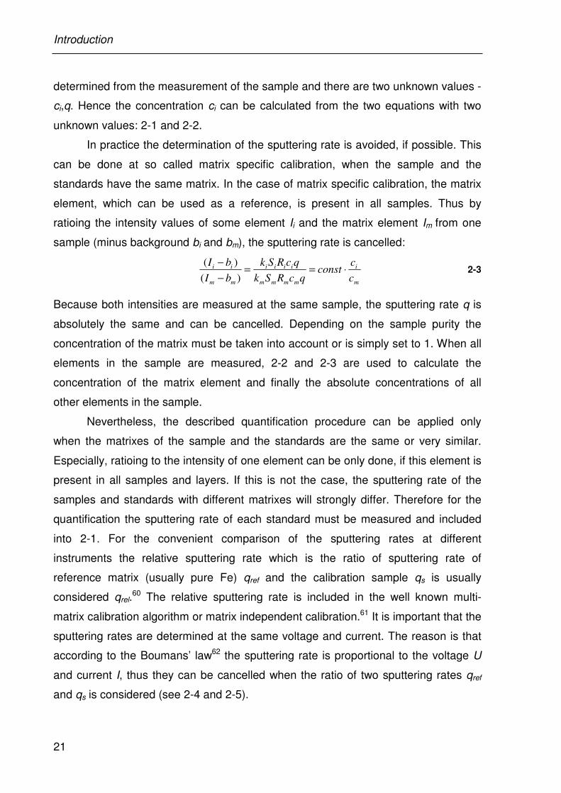
iiiiii bqcRSkI += 2-1
First of all the intensity Ii of the characteristic light of element i depends on the
concentration of this element in the sample ci [m%]. The sputtering rate of the sample
q [µg/s] is responsible for the supply of the sputtered atoms and is a constant when
the sputtered matrix doesn’t change. The process of excitation – de-excitation is
characterized by the emission yield Ri of the element i in the plasma and by the
correction of self-absorption Si. The detection process is taken into account by
introduction of the instrumental detection efficiency ki. bi – is a background value
which depends on the individual instrument. In any analysis it should be assumed
that the concentrations of all elements will add up to 100% (see 2-2).58
1=∑i
ic 2-2
The emission yield Ri is the number of photons with defined wavelength emitted per
atom or ion of element i in the plasma. Ri can be determined from the measurement
of standard samples with known concentration of element i. The advantage of GD
sputtering is that the sputtering and excitation processes are separated in space and
time; therefore the excitation or the emission yield of the sputtered particle is
independent of the sputtered matrix. Thus the emission yield determined from the
measurement of a standard sample is valid also for an unknown sample with different
matrix and can be used for quantification. However this assumption is valid only
when standard and unknown sample are sputtered under the same electrical
conditions, particularly the same voltage and current. This theory is known as “the
concept of constant emission yield” with the main principle that the emission yield is
almost matrix- and pressure-independent but strongly influenced by voltage and
current.59
Summarizing, the Ri is determined from the standards, the ki, Si, bi and
sputtering rate q (only when the sputtered matrix is the same) are constants, the Ii is
Introduction
21
determined from the measurement of the sample and there are two unknown values -
ci,q. Hence the concentration ci can be calculated from the two equations with two
unknown values: 2-1 and 2-2.
In practice the determination of the sputtering rate is avoided, if possible. This
can be done at so called matrix specific calibration, when the sample and the
standards have the same matrix. In the case of matrix specific calibration, the matrix
element, which can be used as a reference, is present in all samples. Thus by
ratioing the intensity values of some element Ii and the matrix element Im from one
sample (minus background bi and bm), the sputtering rate is cancelled:
m
i
mmmm
iiii
mm
ii
c
cconst
qcRSk
qcRSk
bI
bI⋅==
−
−
)(
)( 2-3
Because both intensities are measured at the same sample, the sputtering rate q is
absolutely the same and can be cancelled. Depending on the sample purity the
concentration of the matrix must be taken into account or is simply set to 1. When all
elements in the sample are measured, 2-2 and 2-3 are used to calculate the
concentration of the matrix element and finally the absolute concentrations of all
other elements in the sample.
Nevertheless, the described quantification procedure can be applied only
when the matrixes of the sample and the standards are the same or very similar.
Especially, ratioing to the intensity of one element can be only done, if this element is
present in all samples and layers. If this is not the case, the sputtering rate of the
samples and standards with different matrixes will strongly differ. Therefore for the
quantification the sputtering rate of each standard must be measured and included
into 2-1. For the convenient comparison of the sputtering rates at different
instruments the relative sputtering rate which is the ratio of sputtering rate of
reference matrix (usually pure Fe) qref and the calibration sample qs is usually
considered qrel.60 The relative sputtering rate is included in the well known multi-
matrix calibration algorithm or matrix independent calibration.61 It is important that the
sputtering rates are determined at the same voltage and current. The reason is that
according to the Boumans’ law62 the sputtering rate is proportional to the voltage U
and current I, thus they can be cancelled when the ratio of two sputtering rates qref
and qs is considered (see 2-4 and 2-5).
Introduction
22
)( 0UUCIq −= 2-4
)(
)(
0
0
UUIC
UUIC
q
s
ref
s
ref
rel−
−== 2-5
In the equation 2-4 U0 is a material dependent threshold voltage; C is a constant
depending on the material.
In some cases it is not possible to keep U and I constant within the
measurement. Therefore a special algorithm to compensate the variations of the
excitation conditions by means of empirically derived expressions was developed.63
For this the emission intensities were measured at different voltages and currents.
The observed dependencies were fitted to mathematical models giving the empirical
intensity expression (see 2-6 and 2-7).
)(UfCIckIA
iii = 2-6
3
3
2
210)( UaUaUaaUf +++= 2-7
The equations 2-6 and 2-7 show that the experimentally deduced intensity depends
exponentially on current and polynomial on voltage. The matrix-independent
constants (A, a0, a1, a2 and a3) are experimentally determined for a number of
spectral lines. Thus with known U and I one can normalize the emission intensity to a
standard voltage and current.
After conversion of the emission intensity to the concentration, the sputtering time
should be converted into the depth. For this the density of the sample is calculated as
the sum of the pure element densities ρi multiplied by their atomic fraction cAi in the
sample:
∑=i
iiAc ρρ 2-8
This assumption about the sample density is valid for metals and alloys;64 however
for the light elements it can bring some errors into the calculated depth. The
calculation of the sputtered depth ∆d within the time interval ∆t and at an anode area
O [cm2] is done according to 2-9:
)/( ρOtqd ∆=∆ 2-9
Introduction
23
The quantification algorithm is repeated for each time interval ∆t. Thus the overall
sputtered depth d is the sum of all ∆d (see 2-10).
∑∆=j
jdd 2-10
2.2.3 GD OES vs. other depth profiling methods
Along with GD OES, GD MS, SIMS, SNMS, AES and XPS are also often used for
depth profiling. The choice of the method depends on several criteria: the
concentration range to measure, the analysis time, the elements to detect, the
thickness of the layers in the sample, the required spatial resolution and of course
the measurement cost. For the trace element analysis in the ng/g concentration
range the mass spectrometric methods like GD MS, SIMS and SNMS are beyond
comparison. But up to µg/g concentrations GD OES is preferable. In comparative
studies GD OES was reported to be the fastest depth profiling method.65-68 The
reason is the previously discussed fast erosion rate in the GD plasma (see paragraph
2.1.2). In addition, GD OES devices are easy to use and have a high sample
throughput because no ultrahigh vacuum is required and the sample can be simply
exchanged. This also results in a reduction of the analysis costs – 100-150 euro for
the measurement. For comparison a MS measurement costs 500-1000 euro.
As compared to the depth profiling methods, which are using high vacuum ion
beam sputtering, GD OES has less matrix effects and therefore the quantification
procedure is less complicated for GD OES. Nevertheless, in contrast to XPS and
AES, GD OES doesn’t provide any information about the chemical bonds in the
sample. The lateral resolution of GD OES is limited by the anode diameter (minimum
1 mm) whereas the lateral resolution of SIMS, SNMS, XPS and AES is in the nm to
µm region.66 Good lateral resolution is a big advantage for the analysis of the thin
and ultrathin layers. In addition, ion beam sputtering allows avoiding the effect of the
sputtered crater on the depth resolution by exclusion of the crater edges from the
area of investigation. On the other hand, GD OES is proved to be also a reliable
depth profiling method for very thin (nm region) layered samples.69 Since the GD
OES is a relatively new depth profiling technique, there are several possibilities to
improve its depth resolution. The depth resolution is mostly affected by the non
Introduction
24
planar sputtered crater. Thus the measured depth profile is a function of the true
depth profile and some response function, which is determined by the sputtering
crater shape. There are several works where the response function was
mathematically described and deconvoluted from the measured depth profile,
providing evident improvement of the depth resolution.70-72 The depth resolution in
GD OES can be improved also experimentally by the application of novel sputtering
conditions. Nowadays pulsed glow discharge is becoming more and more popular in
GD OES and GD MS due to the ability to control the sputtering rates and crater
shapes with greater precision. Pulsed glow discharge will be detailed discussed in
the following paragraphs.
2.3 Pulsed glow discharge (PGD)
2.3.1 Virtues and shortcomings of the pulsed mode
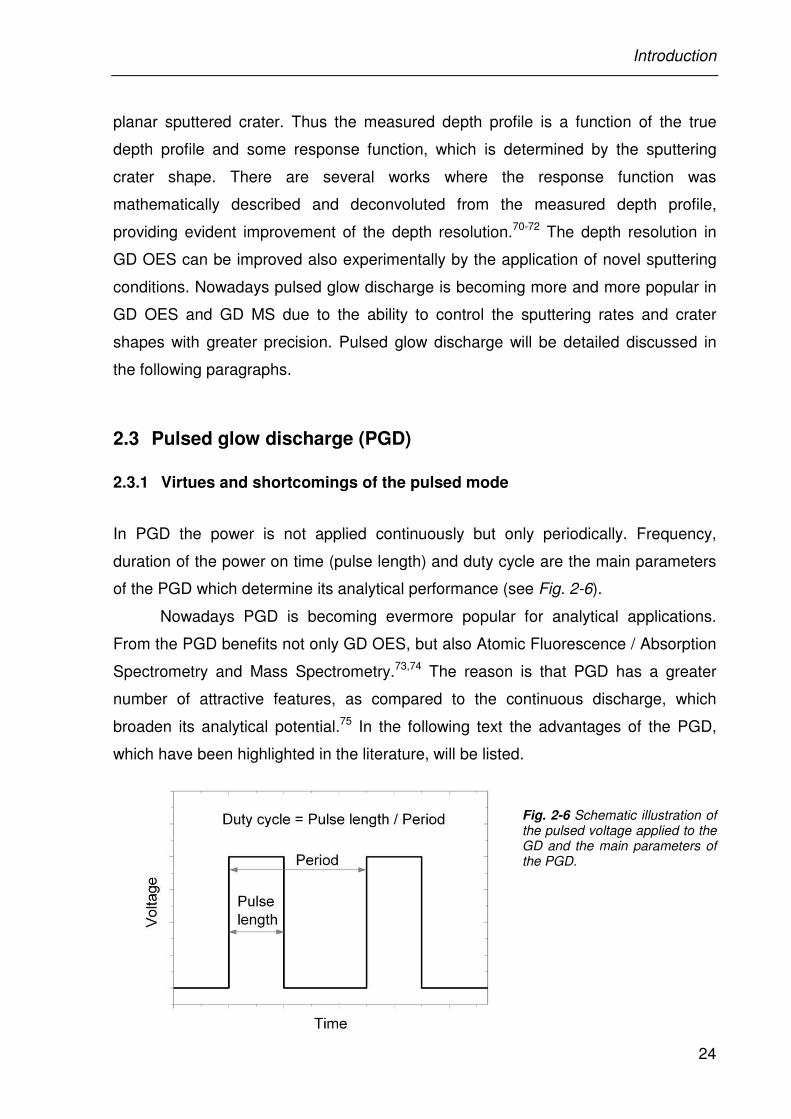
In PGD the power is not applied continuously but only periodically. Frequency,
duration of the power on time (pulse length) and duty cycle are the main parameters
of the PGD which determine its analytical performance (see Fig. 2-6).
Nowadays PGD is becoming evermore popular for analytical applications.
From the PGD benefits not only GD OES, but also Atomic Fluorescence / Absorption
Spectrometry and Mass Spectrometry.73,74 The reason is that PGD has a greater
number of attractive features, as compared to the continuous discharge, which
broaden its analytical potential.75 In the following text the advantages of the PGD,
which have been highlighted in the literature, will be listed.
Fig. 2-6 Schematic illustration of the pulsed voltage applied to the GD and the main parameters of the PGD.
Introduction
25
Additional control parameters Besides the common GD parameters – voltage,
current and pressure - the pulsed discharge has a duty cycle, pulse duration and
frequency. With these additional parameters the sample removal rate can be
controlled with greater precision. Thin films that would be immediately removed in the
continuous discharge, show moderate sputtering rates with PGD.76-79
Reduction of the sample heating In steady-state discharges the sample being
analyzed must continuously dissipate heat that is produced in the sputtering process,
which leads to the sample heating. Thus the continuous discharge is limited by the
power level which can be tolerated by the sample. It was found that the sample and
the discharge gas temperature affect the depth resolution and the sputtering rate.80,81
Too high temperature can even partly melt82 or mechanically destroy the sample. The
application of PGD reduces the sample heating during the analysis and thereby
promotes a good depth resolution. Thus with PGD also thermally fragile samples can
be analysed.83-87
As a result of the reduced sample heating, PGDs allow higher transient
powers than continuous discharges. Typical voltage ranges are 600 – 1200 V and
600 - 3000 V for the continuous and pulsed dc modes respectively. Likewise, the
currents are also considerably different – tens of mA for the continuous mode versus
tens to hundreds of mA of transient current in the pulsed dc discharge.
Enhanced ionisation and excitation efficiency Because of the higher voltages and
transient currents of PGD the ionisation and excitation efficiency within the pulse is
also higher. By gating the detector to acquire the signal only during the pulse, the
analytical signal may be maximized.88-90 The gated detection and investigations of
the temporal emission and ionisation within the pulse revealed a number of useful
effects. For example an interesting feature of PGD is the reduction of self-absorption
at the very beginning of the pulse (first µs). This effect is relevant for the GD OES
quantification, because the curvature of the calibration curves was observed to be
reduced when only the first microseconds of the pulse are detected.74,91
Introduction
26
Temporal resolution The pulsing process initiates different excitation and ionization
mechanisms at the beginning, during and after the pulse with strong, medium and
soft plasma conditions.92-94 Using this feature and time-of-flight mass spectrometry
one can extract elemental and molecular information from gaseous samples.95-98
Recent studies have shown that the direct oxidation state determination is also
possible in solid state materials.99,100 In addition by measuring the emission at a
defined time of the pulse one can discriminate the impact of contaminations or other
species in the plasma.101-103
In spite of the above-listed advantages of the PGD, its use in commercial
spectrometers has still some limitations. Firstly, on the one hand, additional control
parameters give bigger room for the sputtering control, but on the other hand, more
parameters complicate the analysis. To find proper measurement conditions one
should study the influence of all discharge parameters on the analytical discharge
performance (depth resolution, light emission, quantification). As the PGD is a
relatively new technique, the parameters of the PGD are not yet comprehensively
investigated. Secondly, it is difficult to quantify the profiles measured with PGD,
because the existing quantification model (see 2.2.2) is established for the
continuous discharge. Therefore, PGD is applied in modern commercial devices
mostly for qualitative analysis. In addition there are two more questions, which are
discussed in the following text (see 2.3.2 and 2.3.3).
2.3.2 Rf or dc pulsing?
PGD, as well as continuous discharge, can be operated either in direct current (dc) or
in radio frequency (rf) mode. The main difference between rf and dc modes is that
the rf discharge is able to sputter nonconductive samples. The simplified description
of the rf discharge processes is given in the following text. For analytical applications,
the rf voltage is delivered to the source through a capacitor. When the rf voltage is
applied, the surface is bombarded alternatively by positive ions and negative
electrons. The rf voltage is sinusoidal and bipolar. Therefore the ionic bombardment,
which is necessary for sputtering, should take 50 % of the whole rf cycle. However
after some rf cycles the surface potential shifts to a negative value providing almost
Introduction
27
continuous ion bombardment.104 The reason for this is that the electrons in the
plasma move much faster than massive ions and consequently the electron current is
greater than the ionic one. Because of the capacitive coupling no net current can flow
through the cathode. Therefore the electrons remain at the cathode surface within
the positive rf cycle. The slow ion flux within the negative rf cycle is not sufficient to
compensate this negative charge formed by electrons. So the excessive negative
charge remains at the cathode surface and the surface potential gets a negative
offset, which is also called dc bias. In this way in case of a conductive sample
(cathode) the capacitor between the rf generator and the source is responsible for
the biasing of the rf voltage to a negative value and sputtering of the sample by
positive ions. 105,106 In case of a nonconductive sample (cathode) the sample itself
acts as a capacitor, preventing the net current flow through the system. Thus the
bombarding electrons also form an electron sheath on the sample surface,
responsible for the cathode sputtering.107
Sometimes the rf mode is advantageous for the analysis of conductive
samples as well, because it is less affected by nonconductive surface oxide
contamination.88
The ability of insulator sputtering is the only difference between rf and dc
discharges which is well known and widely applied for the analysis. Further
comparison of the dc and rf discharges is still the topic of debates. In the following
text references will be highlighted where some authors suppose that ionisation and
sputtering efficiencies are different in dc and rf modes, and others which believe that
both modes are similar.
It has been reported that in rf discharges two different discharge regimes exist:
α and γ.74,108,109 In the α regime the electrons in the bulk plasma are heated by the rf
field oscillations. The energy of these electrons is high enough to cause ionisation
and to sustain the plasma. In case of the γ regime the discharge is sustained by the
electrons emitted from the cathode (secondary electrons). In dc discharges only the γ
regime exists. The absence of the α regime and also computational results indicate
that the ionization in dc mode is less efficient than in the rf one.109,110 However, later
modelling studies have shown that the calculated Cu atom and ion densities, optical
emission spectra, sputtering rates and sputter crater shapes are similar for rf and dc
Introduction
28
mode. These computational results are in good agreement with experimental data.111
Lewis et al. studied the temporal emission characteristics of pulsed dc and rf
discharges and found only negligible differences between dc and rf mode.112 Präßler
et al. have observed that the GD OES intensity-time profiles, crater shapes and
depth resolution are similar for rf and dc discharges.113 Alberts et al. have
investigated the emission pre-peak of the pulsed discharge and observed similar
behaviour for both rf and dc modes.91 On the other hand, a Langmuir probe study of
the rf glow discharge has shown that the electron energy and temperature are higher
for the rf mode than those for the dc one.114 In addition Harrison et al. have
mentioned that the efficiency of sputtering by an rf discharge is somewhat less than
that obtained by dc.88
Thus, from the literature it is difficult to conclude wether the dc and rf modes
are different or similar. At this point it is extremely important to emphasize at which
electrical conditions these two modes are compared. Two discharges can be
compared at the same pressure and only in the case when the power they are
consuming is the same. Hence, for the case of rf discharges equivalents to the dc-
voltage and dc-current are necessary. Bogaerts et al. have made the first mention
about the conditions at which rf and dc discharges should be compared: “in the dc
discharge a higher operating voltage was needed to yield the same amount of power,
compared to the corresponding dc bias voltage in the rf discharge”.109 Additional
studies115 and subsequent work105 have shown that the rf equivalent of the dc voltage
is the effective voltage Ueff, which is the cycle root mean square value of the periodic
voltage signal Up(t) plus bias Ubias (see 2-11). Indeed, as Bogaerts mentioned, the
Ueff is a little higher than the dc bias. The equivalent for the current value Ieff is the rf
power P divided by the effective voltage (see equations 2-12, 2-13, 2-14).
∫ −−=pt
o
pbias
p
eff dttUUt
U 2))((1
2-11
)()()( tItUtP pp ⋅= 2-12
dttPt
P
pt
t
p
)(1
0
∫= 2-13
Introduction
29
eff
effU
PI = 2-14
It must be mentioned that the determination of power, rf voltage and dc bias
deteriorates with increasing thickness of insulating samples. The quality of the power
measurement at fixed frequency generator systems depends on the power losses in
the matchbox and the quality of the used correction – the so-called subtraction
method. The rf voltage becomes lower throughout nonconductive samples,
depending on sample thickness, frequency and current. In principle, this voltage loss
can be corrected, if voltage and current are measured. The direct measurement of
the dc bias becomes totally impossible and calculation procedures105 or
estimations115 must be used.
In conclusion, there is no work where the dc and rf discharges are
comprehensive compared. The pulsed discharge is even less studied. However it is
shown that for the comparative studies the effective voltage in the rf mode should be
used as an equivalent to the dc voltage.
2.3.3 How big is the thermal stress reduction when PGD is applied?
One of the outstanding possibilities of PGD is the reduction of thermal stress caused
by sputtering (see 2.3.1). The heating of the discharge cell, in particular of the
cathode and the discharge gas, is a phenomenon frequently associated with GD
studies and applications. A number of publications, experimental and modeling
studies, have reported the considerable impact of the discharge gas and sample
heating. For example, it has been observed that the GD OES depth profile of a Zn-
on-steel thin film sample is changing being analyzed either with or without sample
cooling.80 Windawi has found a variation of the Cu sputtering yield when its
temperature is varied.81 Heyner et al. have shown that too high temperature can even
partly melt the sample.82 The cathode temperature has been identified as an
important parameter influencing the mass loss due to evaporation for zinc cathodes
in analytical glow discharge.116 Wilken et al. have found that the sample expands at
the moment of the plasma ignition and explained this effect by the increased
sputtered surface temperature.117 Experimental studies have shown that the
Introduction
30
discharge gas temperature influences the discharge current at constant voltage and
pressure: a temperature rise results in a decrease of the gas density, and thus
causes a decrease of the discharge current.2,118-121 This phenomenon has also been
confirmed by modeling results.122-124
In spite of the above-listed thermal effects and their considerable impact on
the GD performance, gas temperature and cathode (or sample) temperature
measurements are not often made in analytical GD spectrometry. However, for the
fundamental studies and analytical applications of PGD it is worthwhile to determine
the extent of thermal stress reduction when pulses are applied. It is also important to
study how the pulsing parameters (duty cycle, pulse duration and frequency)
influence the discharge gas and sample temperature. As of today there are only few
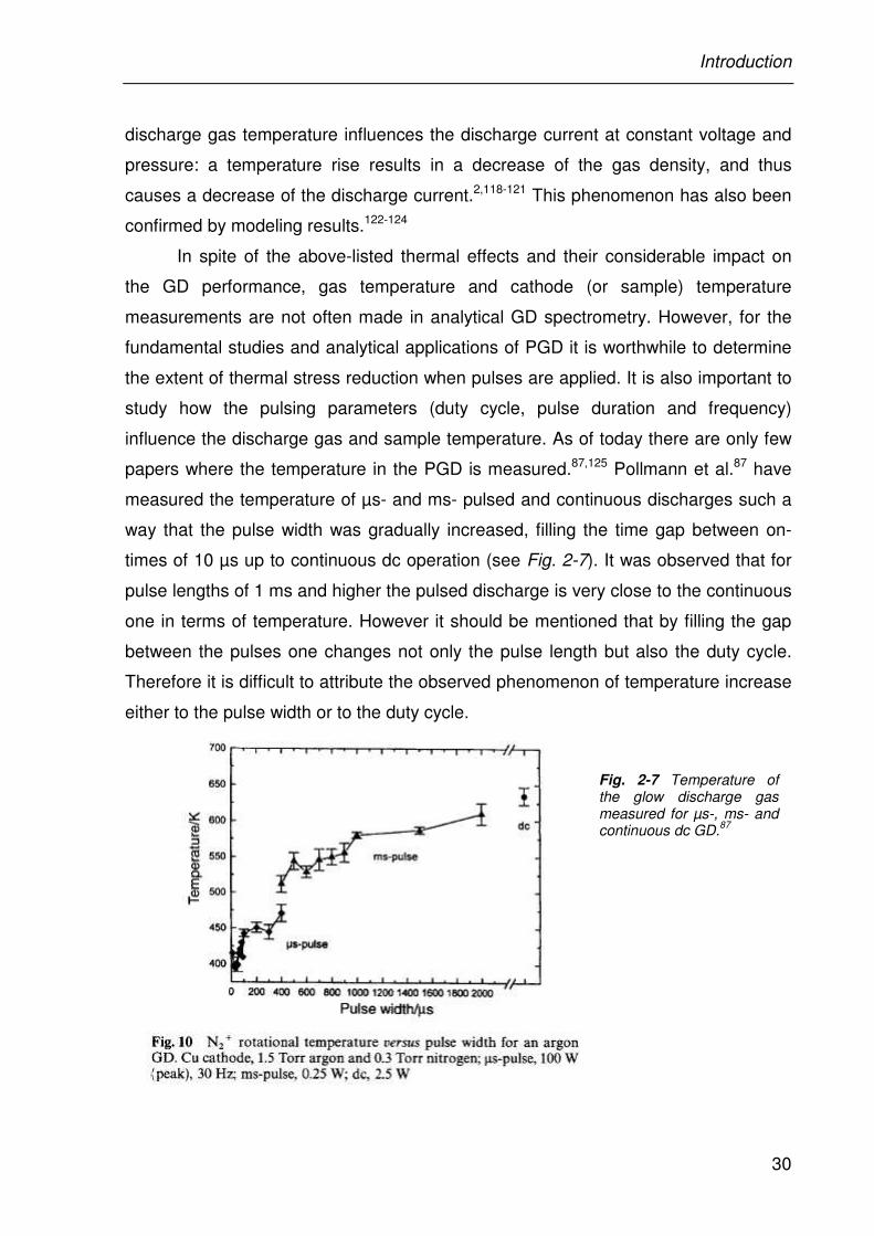
papers where the temperature in the PGD is measured.87,125 Pollmann et al.87 have
measured the temperature of µs- and ms- pulsed and continuous discharges such a
way that the pulse width was gradually increased, filling the time gap between on-
times of 10 µs up to continuous dc operation (see Fig. 2-7). It was observed that for
pulse lengths of 1 ms and higher the pulsed discharge is very close to the continuous
one in terms of temperature. However it should be mentioned that by filling the gap
between the pulses one changes not only the pulse length but also the duty cycle.
Therefore it is difficult to attribute the observed phenomenon of temperature increase
either to the pulse width or to the duty cycle.
Fig. 2-7 Temperature of the glow discharge gas measured for µs-, ms- and continuous dc GD.
87
Introduction
31
Jackson et al.125 and Gamez et al.126 have also measured the gas temperature of the
ms-pulsed GD, but have paid more attention on the spatial temperature distribution
above the cathode than on the influence of the pulsing parameters.
The lack of temperature studies in PGD is caused by the complexity of the
temperature measurement techniques. In the following chapter the methods of the
discharge gas temperature measurement and the corresponding complications are
briefly discussed.
2.4 Measurement of the discharge gas temperature
2.4.1 What is the temperature of the glow discharge gas?
Temperature relates to the thermal energy held by a matter, which is the kinetic
energy of the random motion of the particle constituents of matter. The empirical
definition of temperature arises from the conditions of thermodynamic equilibrium,
expressed as the zeroth law of thermodynamics: “Systems are in thermal equilibrium
if they do not exchange energy in the form of heat.” Hence the gas temperature is
characterized by the kinetic energy of the gas particles when these particles are in
the thermodynamic equilibrium (TE) with each other. Therefore, to understand what
is the temperature of the GD gas one should examine the particles in the GD and
their temperatures as well as the conditions of TE. It is well known that the GD gas
contains several types of particles: electrons, photons, ions, neutral atoms, excited
atoms and ions and also molecules or radicals. Thus the GD can be characterized by
different temperatures:
1. The electron temperature, which represents the kinetic energy of the electrons;
2. The neutral atom temperature, which characterizes the kinetic energy of the
neutral atoms;
3. The excitation temperature, which describes the population of the various energy
levels;
4. The ionization temperature, which governs the ionization equilibrium;
5. The rotational and vibrational temperatures of the molecules.
Introduction
32
If the GD gas were in TE, a single temperature value might describe all the above-
listed temperatures. Also the conditions of the TE would have to be fulfilled for the
GD:
1. The velocity distribution of all kinds of free particles (molecules, atoms, ions and
electrons) in all energy levels satisfies the Maxwell’s equation;
2. For each separate kind of particle the relative population of energy levels conforms
to Boltzmann’s distribution law.
3. Ionization of atoms, molecules and radicals is described by the Saha’s equation
and dissociation of molecules and radicals by the general equation for chemical
equilibrium.
4. Radiation density is consistent with Planck’s law.127-129
Nevertheless it is well known that in the GD the electron temperature is much higher
than the temperature of the other massive particles in the plasma: 10000 K versus
less than 1000 K.9,130,131 The reason is that the electrons continuously acquire the
energy in the electric field, but the energy transfer by means of elastic collisions from
the light electrons to the much heavier particles in the plasma is inefficient. In
addition the walls of the GD cell have a temperature different from the GD gas and
the discharge gas flow brings cold gas into the plasma; thus there is a heat exchange
in the system and some processes cannot be in equilibrium with their converse. Also
the velocity of the charged plasma particles depends not only on the temperature, as
it should be in TE, but also on the applied electric field. So it can be concluded that
the GD gas is not in thermodynamic equilibrium.130 It has to be noted that when the
gas is not in the TE a physical meaning for the gas temperature becomes vague.
Nevertheless the TE approach allows using the well known equations (see conditions
of TE above) to interpret the spectral line intensities and to simulate the plasma, what
is much simpler and faster than solving the non-thermal equations.132,133 Therefore
for plasmas which are close to thermal ones different approximations are usually
done. However one should be cautious in using these approximations because they
can cause unexpected errors for plasmas strongly departing from the TE. Thus there
are several criteria which help to estimate whether the plasma is predominantly
thermal or not.134-138 For the plasmas where the temperature gradient is small
(comparable with the distance at which the excited atom diffuses during its
Introduction
33
relaxation) and where the particles exchange their energy very frequently (collision
frequency is 10 times larger than the radiation frequency) each small portion of the
gaseous body can be characterized by a unique temperature. The equilibrium
conditions in such a non-homogeneous gas are called local thermodynamic
equilibrium (LTE).128,129,137 For the LTE the Boltzmann and Saha’s equations are
valid. The particle temperatures in the GD plasma, especially when comparing
electrons with atoms or ions, differ from each other. Therefore the GD gas is not in
LTE. On the other hand the GD is a weakly ionized plasma with an ionization degree
of less than 1 % and the number of electrons and ions in the plasma is much smaller
than the neutral atoms.7,139 Thus the particle velocity in the GD gas depends to a
lesser extent on the electric field than on the temperature. Also the huge electron
temperature has a small effect on the establishment of the LTE in the GD gas,
because the electrons are not capable to change the kinetic energy of the other
much heavier plasma particles significantly. So the GD gas can be assumed to be
close to the LTE. LTE can only be expected if collisional processes are more
important than radiative decay and recombination, and if the velocity distributions of
the colliding particles are thermal. Since most collisional excitations and ionizations
and their inverses involve electrons, the electron density mostly determines how
close the GD gas is to the LTE.137
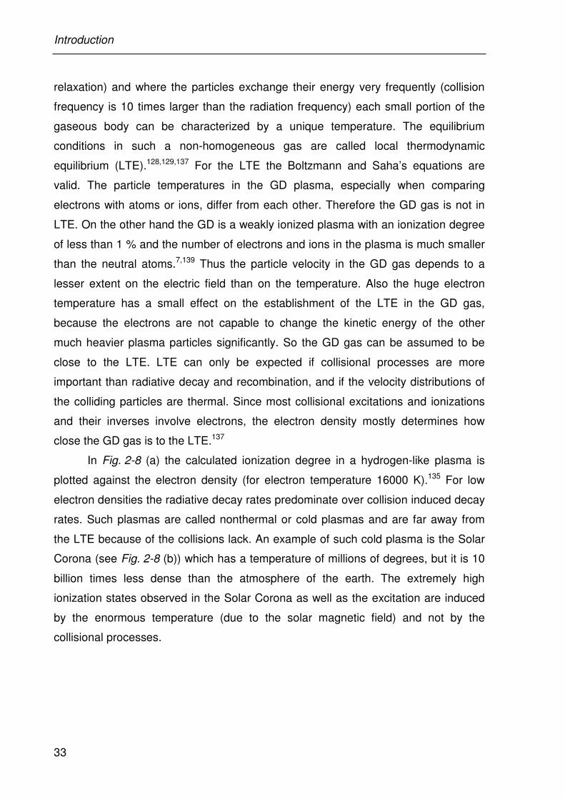
In Fig. 2-8 (a) the calculated ionization degree in a hydrogen-like plasma is
plotted against the electron density (for electron temperature 16000 K).135 For low
electron densities the radiative decay rates predominate over collision induced decay
rates. Such plasmas are called nonthermal or cold plasmas and are far away from
the LTE because of the collisions lack. An example of such cold plasma is the Solar
Corona (see Fig. 2-8 (b)) which has a temperature of millions of degrees, but it is 10
billion times less dense than the atmosphere of the earth. The extremely high
ionization states observed in the Solar Corona as well as the excitation are induced
by the enormous temperature (due to the solar magnetic field) and not by the
collisional processes.
Introduction
34
Fig. 2-8 (a) Ionization ration versus electron density measured for a hydrogen plasma
135 and (b) classification of plasmas in dependence on electron temperature
and density .140
The other extreme case is on the right side of Fig. 2-8 (a) and (b), which correspond
to high electron densities and thus to a complete LTE. In this area collision induced
decay dominates and all atomic levels have a thermal population, i.e. the Boltzmann
and Saha equations are valid. An example of a thermal plasma is the Sun Core
(thermal fusion plasmas in Fig. 2-8 (b)). The core is made of hot dense gas in the
plasmic state, which has a density of up to 150000 kg/m³ (150 times the density of
liquid water) and a temperature close to 15000000 K.
The GD plasma has an electron density of around 1015 cm-3 as can be seen
from Fig. 2-8 and is between the nonthermal and thermal plasmas.7,141,142 From
Fig. 2-8 one can see that depending on the electron density the GD plasma is either
close to a nonthermal or to a thermal plasma (dashed lines). Consequently the
further the GD plasma deviates from thermal one, the higher is the error which one
introduces using the thermal equations. For the GD and also similar plasmas it is
useful to apply the concept of partial LTE where only a limited range of energy levels
of electrons in the atoms and ions can be described by the Boltzmann and Saha
equations. It is known that in the collisional-radiative processes the upper levels
reach a thermal distribution with a continuum of free electrons more easily than the
lower levels. Thus one assumes that ions or atoms are in partial LTE if the population
density of one of theirs levels and all higher-lying levels can be described by the
Boltzmann and Saha equations.134 Therefore, an energy level for the electrons in
Introduction
35
ions or atoms exists, which can be called “thermal limit”, above which the
distributions approximate to thermal and below which they are approximately
nonthermal. As the electron density increases, the “thermal limit” drops lower and
lower; at sufficient high densities it reaches the ground level and all levels have
thermal population.135
In conclusion, it was shown that the definition of the GD gas temperature is not
trivial. However it can be assumed that the GD gas temperature is characterized by
the kinetic temperature of the plasma particles which are mostly close to the thermal
gas particles, in particular – neutral atoms, metastable atoms, some ions (generally in
the negative glow region where the electric field is not very strong) and molecules.
The approximation of the nonthermal GD gas to the thermal one can cause some
inaccuracies or even errors in both computational studies and interpretation of the
emission spectra.
2.4.2 Determination of the GD temperature from the rotational spectra of the
molecules
The discharge gas temperature is often determined from the rotational spectra of
diatomic molecules in the plasma (usually N2 or OH radicals).87,125,143-149 The
rotational temperature Trot is assumed to have generally the same magnitude as the
gas kinetic temperature because of the low energies involved in the rotational
process and the rapid exchange between rotational and kinetic energy of the
molecule. In other words when the discharge gas is in LTE, the rotational
temperature of the molecule in this gas should be equal to the kinetic gas
temperature. In this case the ratio of population or number density nk of bound
electrons at the rotational level with energy Ek and total number density of the
rotational states n is described by the Boltzmann distribution:
)(/)]/exp([/ TQkTEgnn rotkkk −= 2-15
where gk is the statistical weight of level k and Q(T) is the partition function which is
very close to the statistical weight of the ground state go at low temperatures.
The emission line intensity I is the product of number density nk and transition
probability A (s-1) for spontaneous emission:
Introduction
36
kAnhI )4/( πν= 2-16
Thus the intensity of a rotational line can be deduced from the equations 2-15 and 2-
16:
)/exp(3
rotk kTESDI −= ν 2-17
where the coefficient D contains the rotational partition function, the statistical weight
g=(2K´+1) and universal constants, S is the oscillator strength. Ek is the rotational
energy:
)1´´( += KhcKBEk ν 2-18
where Bν is a rotational constant belonging to the vibrational quantum number ν, and
K´ is the quantum number of the rotational level or the angular momentum.
From the 2-17 and 2-18 follows:
constKKkT
hcBSI
rot
++−= )1´´()/log( ν 2-19
The line strength S, the constants Bν, h, c, k and K´ are known from the literature.
Thus the rotational temperature Trot of the molecule can be determined from the
slope of the plot: log(I/S) vs K´(K´+1) plotted for the measured intensities of the
rotational lines from one vibrational band of the molecule.150
The Boltzmann plot method is often used for the determination of the
discharge gas temperature, because of its simplicity and the possibility of spatial
resolved measurements (e.g. at side-on intensity measurements). This method
doesn’t require a very high spectral resolution; therefore the rotational spectra can be
measured with common commercial spectrometers (resolution of around 20 pm).
Moreover when the measured spectrum is partially resolved, a special procedure of
the spectral contour fit can be applied to deduce the rotational temperature.151-153 On
the other hand the determination of the gas temperature by the measurement of
rotational emission line intensities is prone to error. Firstly the rotational temperature
of the molecule may not be similar with the kinetic gas temperature because of the
lack of LTE. In addition the accuracy with which one knows the transition probabilities
of the measured rotational lines is critical. It should be also mentioned that to obtain
measurable rotational spectra of the molecular species it is necessary to add enough
of those species, which can alter the temperature.
Introduction
37
2.4.3 Determination of the GD temperature from the Doppler width of spectral
lines
The phenomenon of Doppler broadening of the spectral lines due to the thermal
motion may be also applied for the determination of the discharge gas
temperature.152,154,155 When the GD gas particles are in thermal motion, i.e. in LTE,
the broadening depends only on the wavelength of the spectral line λ, the mass of
the emitting particles M, and their temperature T, and therefore can be used for
inferring the temperature of an emitting gas:
MT /1016,7 7
2/1 λλ −×=∆ 2-20
where ∆λ1/2 is the full emission line width at half intensity.154,156
The Doppler method of the GD temperature determination requires extremely
high spectral resolution which can be only achieved at special (e.g. Fourier
transform) spectrometers. The operation of these spectrometers is much more
complicated and spectrum measurements are time consuming in contrast to the
commercial low resolution spectrometers. Similarly to the rotational temperature, the
Doppler temperature can deviate from the kinetic gas temperature introducing an
error into the deduced kinetic gas temperature value.
2.4.4 Laser-light scattering technique for the measurement of the GD
temperature
The Rayleigh scattering of the laser on the plasma particles is frequently used for the
determination of the discharge gas temperature.126,131,157-160 Rayleigh scattering of
incident light occurs only from very small particles, and is proportional to the
concentration of the scatterers in the observation volume. In the GD, where the
ground-state argon atoms are by far the most prevalent scatterers, the Rayleigh
scattering is the measure of the localized argon number density. Thus, with known
number density the gas kinetic temperature can be calculated from the ideal gas law.
The laser-light scattering method requires special equipment and can not be
performed with a common GD source at a commercial spectrometer. However the
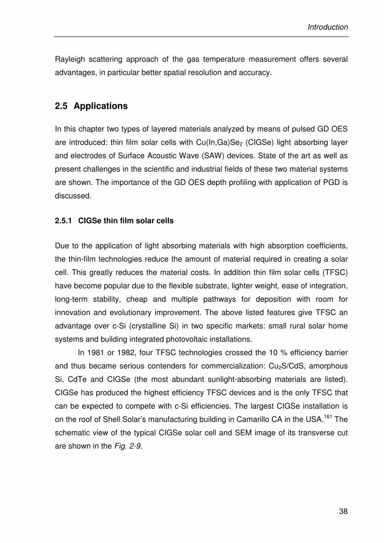
Introduction
38
Rayleigh scattering approach of the gas temperature measurement offers several
advantages, in particular better spatial resolution and accuracy.
2.5 Applications
In this chapter two types of layered materials analyzed by means of pulsed GD OES
are introduced: thin film solar cells with Cu(In,Ga)Se2 (CIGSe) light absorbing layer
and electrodes of Surface Acoustic Wave (SAW) devices. State of the art as well as
present challenges in the scientific and industrial fields of these two material systems
are shown. The importance of the GD OES depth profiling with application of PGD is
discussed.
2.5.1 CIGSe thin film solar cells
Due to the application of light absorbing materials with high absorption coefficients,
the thin-film technologies reduce the amount of material required in creating a solar
cell. This greatly reduces the material costs. In addition thin film solar cells (TFSC)
have become popular due to the flexible substrate, lighter weight, ease of integration,
long-term stability, cheap and multiple pathways for deposition with room for
innovation and evolutionary improvement. The above listed features give TFSC an
advantage over c-Si (crystalline Si) in two specific markets: small rural solar home
systems and building integrated photovoltaic installations.
In 1981 or 1982, four TFSC technologies crossed the 10 % efficiency barrier
and thus became serious contenders for commercialization: Cu2S/CdS, amorphous
Si, CdTe and CIGSe (the most abundant sunlight-absorbing materials are listed).
CIGSe has produced the highest efficiency TFSC devices and is the only TFSC that
can be expected to compete with c-Si efficiencies. The largest CIGSe installation is
on the roof of Shell Solar’s manufacturing building in Camarillo CA in the USA.161 The
schematic view of the typical CIGSe solar cell and SEM image of its transverse cut
are shown in the Fig. 2-9.
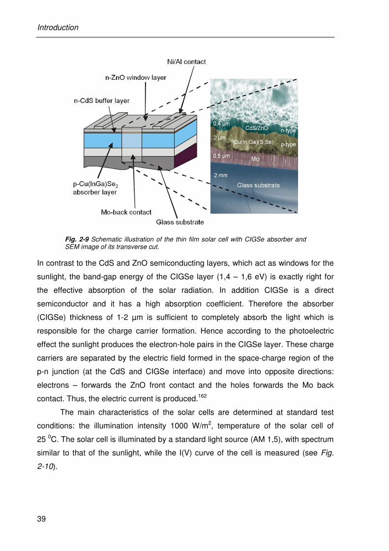
Introduction
39
Fig. 2-9 Schematic illustration of the thin film solar cell with CIGSe absorber and SEM image of its transverse cut.
In contrast to the CdS and ZnO semiconducting layers, which act as windows for the
sunlight, the band-gap energy of the CIGSe layer (1,4 – 1,6 eV) is exactly right for
the effective absorption of the solar radiation. In addition CIGSe is a direct
semiconductor and it has a high absorption coefficient. Therefore the absorber
(CIGSe) thickness of 1-2 µm is sufficient to completely absorb the light which is
responsible for the charge carrier formation. Hence according to the photoelectric
effect the sunlight produces the electron-hole pairs in the CIGSe layer. These charge
carriers are separated by the electric field formed in the space-charge region of the
p-n junction (at the CdS and CIGSe interface) and move into opposite directions:
electrons – forwards the ZnO front contact and the holes forwards the Mo back
contact. Thus, the electric current is produced.162
The main characteristics of the solar cells are determined at standard test
conditions: the illumination intensity 1000 W/m2, temperature of the solar cell of
25 0C. The solar cell is illuminated by a standard light source (AM 1,5), with spectrum
similar to that of the sunlight, while the I(V) curve of the cell is measured (see Fig.
2-10).
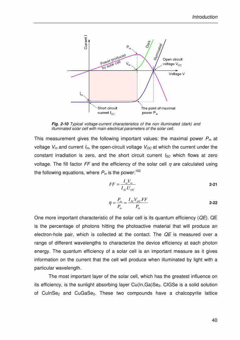
Introduction
40
Fig. 2-10 Typical voltage-current characteristics of the non illuminated (dark) and illuminated solar cell with main electrical parameters of the solar cell.
This measurement gives the following important values: the maximal power Pm at
voltage Vm and current Im, the open-circuit voltage VOC at which the current under the
constant irradiation is zero, and the short circuit current ISC which flows at zero
voltage. The fill factor FF and the efficiency of the solar cell η are calculated using
the following equations, where Pin is the power:162
OCSC
mm
UI
VIFF = 2-21
in
OCSC
in
m
P
FFVI
P
P==η 2-22
One more important characteristic of the solar cell is its quantum efficiency (QE). QE
is the percentage of photons hitting the photoactive material that will produce an
electron-hole pair, which is collected at the contact. The QE is measured over a
range of different wavelengths to characterize the device efficiency at each photon
energy. The quantum efficiency of a solar cell is an important measure as it gives
information on the current that the cell will produce when illuminated by light with a
particular wavelength.
The most important layer of the solar cell, which has the greatest influence on
its efficiency, is the sunlight absorbing layer Cu(In,Ga)Se2. CIGSe is a solid solution
of CuInSe2 and CuGaSe2. These two compounds have a chalcopyrite lattice
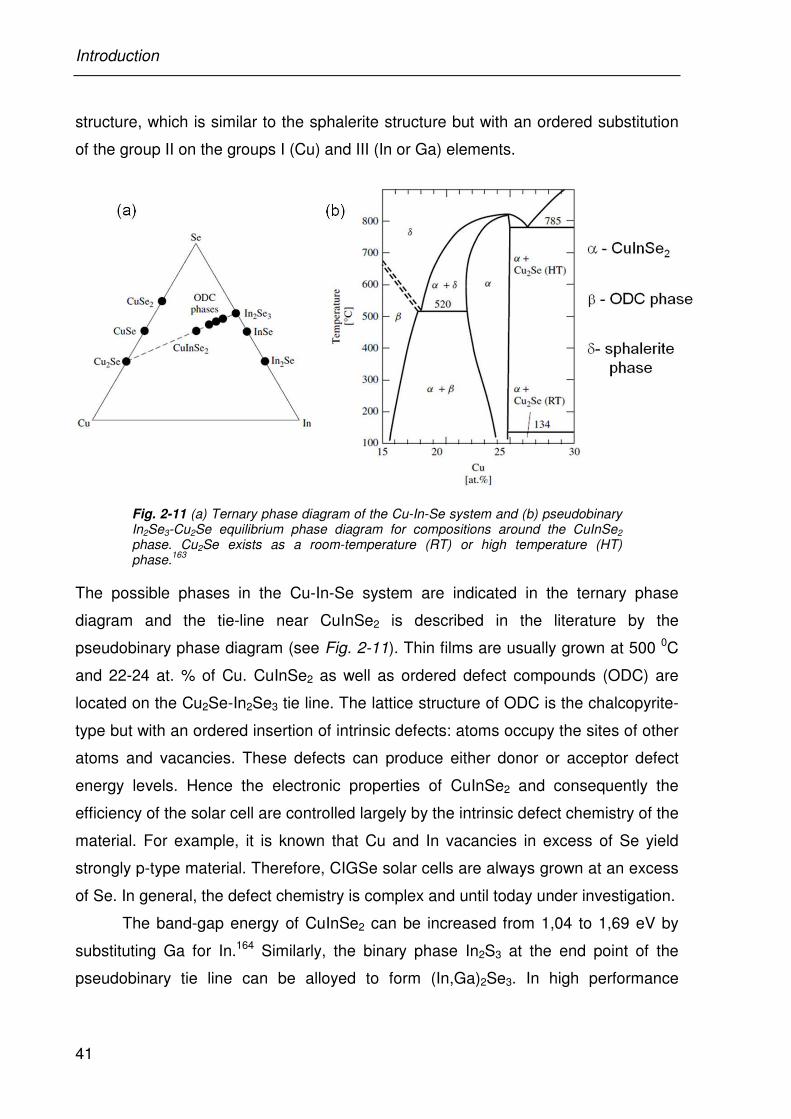
Introduction
41
structure, which is similar to the sphalerite structure but with an ordered substitution
of the group II on the groups I (Cu) and III (In or Ga) elements.
Fig. 2-11 (a) Ternary phase diagram of the Cu-In-Se system and (b) pseudobinary In2Se3-Cu2Se equilibrium phase diagram for compositions around the CuInSe2 phase. Cu2Se exists as a room-temperature (RT) or high temperature (HT) phase.
163
The possible phases in the Cu-In-Se system are indicated in the ternary phase
diagram and the tie-line near CuInSe2 is described in the literature by the
pseudobinary phase diagram (see Fig. 2-11). Thin films are usually grown at 500 0C
and 22-24 at. % of Cu. CuInSe2 as well as ordered defect compounds (ODC) are
located on the Cu2Se-In2Se3 tie line. The lattice structure of ODC is the chalcopyrite-
type but with an ordered insertion of intrinsic defects: atoms occupy the sites of other
atoms and vacancies. These defects can produce either donor or acceptor defect
energy levels. Hence the electronic properties of CuInSe2 and consequently the
efficiency of the solar cell are controlled largely by the intrinsic defect chemistry of the
material. For example, it is known that Cu and In vacancies in excess of Se yield
strongly p-type material. Therefore, CIGSe solar cells are always grown at an excess
of Se. In general, the defect chemistry is complex and until today under investigation.
The band-gap energy of CuInSe2 can be increased from 1,04 to 1,69 eV by
substituting Ga for In.164 Similarly, the binary phase In2S3 at the end point of the
pseudobinary tie line can be alloyed to form (In,Ga)2Se3. In high performance
Introduction
42
devices, the [Ga]/([Ga]+[In]) ratio is typically between 0,2 and 0,3. Substituting Se for
S increases the band gap energy. Further improvements are obtained by
incorporating Na into the CIGSe layer, although the Na role in improving the device
efficiency is not yet completely understood. Soda-lime glass used as substrate
provides uncontrollable source of Na, since during the layer growth at high
temperatures Na diffuses through the Mo layer into the CIGSe. There is a theory that
the chalcopyrite phase field α is increased by the addition of Ga or Na. However the
influence of Na and Ga as well as other elements (for example Zn or Fe) on the
CIGSe solar cells performance is still under study.162,163,165
Summarizing, the elemental composition of the absorber layer has great
influence on the intrinsic defect formation and the band gap of the light absorbing
material, which are crucial for the solar cell efficiency. Also the lateral distribution of
the elements in the absorbing layer has an influence on the solar cell
performance.166,167 Therefore the measurement of the elemental depth-distribution is
relevant for the study of the CIGSe and for a better understanding of its mode of
operation. As shown above, GD OES is a suitable and fast method providing either
qualitative (intensity-sputtering time) or quantitative (concentration-depth) depth
profiles (see 2.2).
Depth profiling is also useful for the development of the solar cells
manufacture as well as for controlling the quality of the deposited layers. There are
two common deposition methods for the CIGSe absorbers: multisource
coevaporation166,167 and two-stage processes of precursor deposition followed by Se
annealing.168,169 Junction and device formation is typically performed by chemical
bath deposition (CdS) and sputtering (ZnO). Despite the level of effort on developing
manufacturing processes, a large discrepancy remains in efficiency between the
laboratory-scale solar cells, and the best large-scale modules. For example, it may
be more cost effective to operate at much higher deposition rate in large-scale
manufacture and to accept a lower efficiency compared with a slower process
optimized for higher efficiency. Hence there is a necessity for developing new
processes and equipment for the large-area and high-throughput deposition, which is
complicated by the lack of a comprehensive scientific base for CIGSe materials and
devices.163

Introduction
43
It was already discussed before that the sputtering procedure at the GD OES
analysis causes heating of the sputtered sample (see 2.3.1). The most abundant
CIGSe substrate is soda lime glass, which is thermally fragile. Therefore, to avoid the
local overheating of the glass during sputtering and its damage due to the thermal
stress, application of the pulsed glow discharge is preferable. The effect of thermal
stress and sputtering on the CIGSe layer is not described in the literature and is
discussed for the first time in the experimental part of the present work.
2.5.2 SAW devices
SAW (Surface Acoustic Wave) devices have got a wide application spectrum due to
their small size and suitability for the large scale production. They are used as high
frequency filters in TV sets, mobile phones, keyless-entry systems, wireless-LAN
products, GPS navigation etc. A schematic drawing of the SAW frequency filter is
shown in the Fig. 2-12.
Fig. 2-12 Schematic drawing of the SAW filter and surface wave transduction by electrodes on piezoelectric substrate.
The electromagnetic radiation is received by the antenna of the SAW filter. If the
frequency of this radiation corresponds to the resonance frequency of the SAW
system, the acoustic surface waves with a well-defined wavelength appear along the
top of the piezoelectric substrate via the inverse piezoelectric effect. Another
electrode system, which is used as a receiver, transforms the mechanical information
of the acoustic wave back into an electrical signal. This way the electromagnetic
radiation with a defined frequency is filtered.170-172
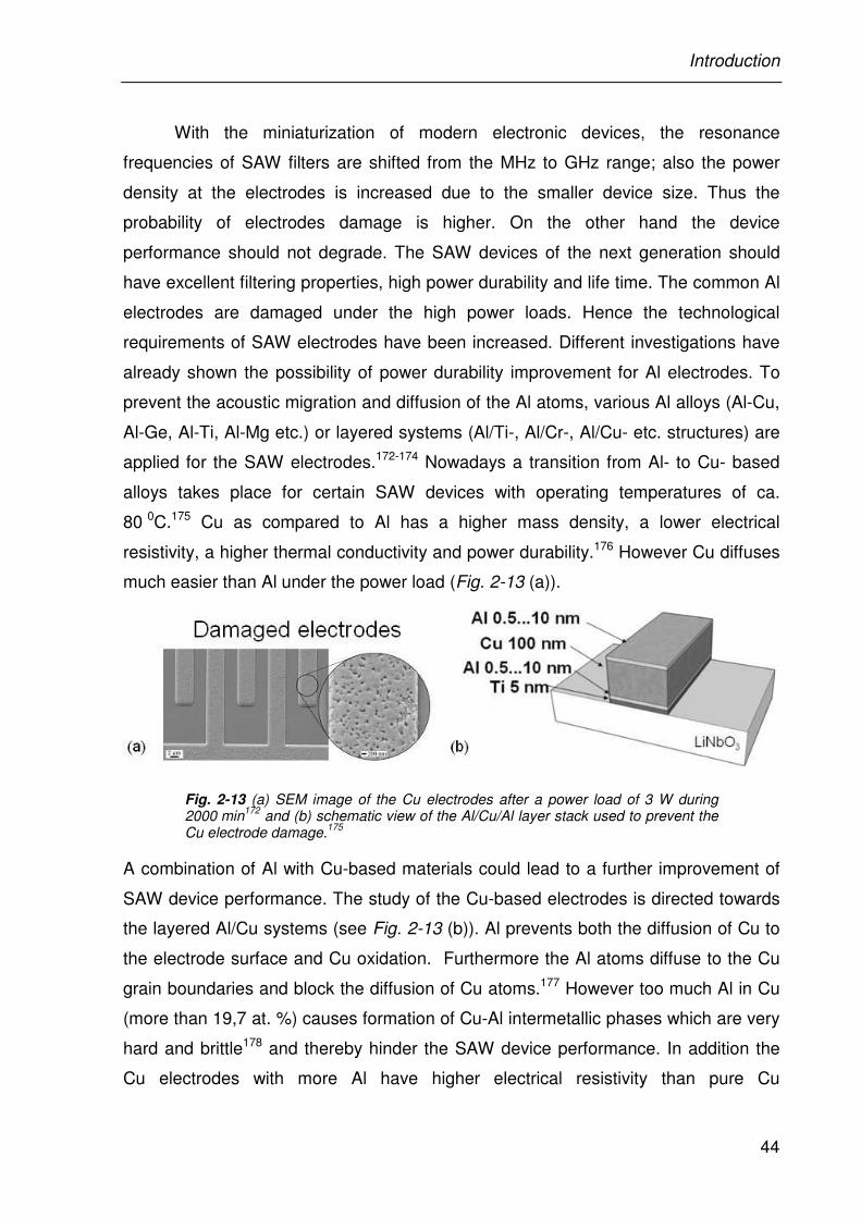
Introduction
44
With the miniaturization of modern electronic devices, the resonance
frequencies of SAW filters are shifted from the MHz to GHz range; also the power
density at the electrodes is increased due to the smaller device size. Thus the
probability of electrodes damage is higher. On the other hand the device
performance should not degrade. The SAW devices of the next generation should
have excellent filtering properties, high power durability and life time. The common Al
electrodes are damaged under the high power loads. Hence the technological
requirements of SAW electrodes have been increased. Different investigations have
already shown the possibility of power durability improvement for Al electrodes. To
prevent the acoustic migration and diffusion of the Al atoms, various Al alloys (Al-Cu,
Al-Ge, Al-Ti, Al-Mg etc.) or layered systems (Al/Ti-, Al/Cr-, Al/Cu- etc. structures) are
applied for the SAW electrodes.172-174 Nowadays a transition from Al- to Cu- based
alloys takes place for certain SAW devices with operating temperatures of ca.
80 0C.175 Cu as compared to Al has a higher mass density, a lower electrical
resistivity, a higher thermal conductivity and power durability.176 However Cu diffuses
much easier than Al under the power load (Fig. 2-13 (a)).
Fig. 2-13 (a) SEM image of the Cu electrodes after a power load of 3 W during 2000 min
172 and (b) schematic view of the Al/Cu/Al layer stack used to prevent the
Cu electrode damage.175
A combination of Al with Cu-based materials could lead to a further improvement of
SAW device performance. The study of the Cu-based electrodes is directed towards
the layered Al/Cu systems (see Fig. 2-13 (b)). Al prevents both the diffusion of Cu to
the electrode surface and Cu oxidation. Furthermore the Al atoms diffuse to the Cu
grain boundaries and block the diffusion of Cu atoms.177 However too much Al in Cu
(more than 19,7 at. %) causes formation of Cu-Al intermetallic phases which are very
hard and brittle178 and thereby hinder the SAW device performance. In addition the
Cu electrodes with more Al have higher electrical resistivity than pure Cu
Introduction
45
electrodes.177 Hence it is essential to find an optimal Al to Cu ratio which provides
both reduced Cu diffusion and oxidation and low electrical resistivity of the
electrodes. GD OES depth profiles of the Al/Cu/Al layer stacks allow controlling the
distribution of Al in Cu. As can be seen from the Fig. 2-13(b) the layers are in the nm
region. Such thin layers would be sputtered within some milliseconds in the
continuous discharge. Therefore to slow down the sputtering of the sample and to
have more control over the sample removal rate, pulsed discharge should be applied.
To characterize the life time of the SAW device the time-to failure (TTF) value
is used. To measure this value the high power loads (1-2 W) and temperatures (50-
100 0C) are applied to the electrodes until they are failing within some acceptable
time. The indicator of the electrode failure is the shift of the SAW filter resonance
frequency (50 kHz-2 MHz).172
46
3 Experimental details
3.1 Measurement of the electrical characteristics
For dc and pulsed dc measurements a 4 mm Grimm-type source from Spectruma is
used. The discharge pressure is measured in the anode body by a Pirani gauge,
calibrated by a Baratron manometer (MKS Baratron Type 127; range 0–100 hPa). A
high voltage generator (MCN 350-2000, FUG) is used to produce the continuous dc
GD. The pulsed dc GD is excited with a high voltage pulse generator (RUP 3-3a,
GBS Elektronik GmbH) and synchronized by an external TTL pulse generator
(33120A, HP). The discharge voltage and the current of the pulsed discharge are
transferred via a digital oscilloscope (11201, Tektronix) to a computer for further
evaluation.
For rf and pulsed rf measurements a modified Grimm-type glow discharge
source with a 4 mm anode tube is used. The GD is excited with a free running rf
generator (Forschungstechnik IFW, 3.37 MHz). The measurements of the transient
voltage and current are made by voltage and current probes integrated into the
source. The experimental setup and the measurement system are described in detail
in the paper of Wilken et al..179 The rf voltage is additionally measured by a 1:100
voltage divider (GE 3425, General Elektronik GmbH). The signals from the voltage
and current probes are fed into a high speed oscilloscope (LC584A, LeCroy) from
which they are subsequently transferred to a PC, where further evaluation is
conducted. For all electrical experiments 10 mm thick pure Cu samples or 0,7 mm
thick Si samples are used.
One part of the present work is dedicated to the optimization of the
experimental setup. This step is essential before performing any experiments to
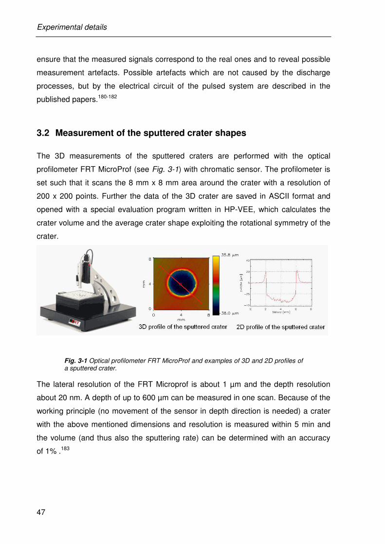
Experimental details
47
ensure that the measured signals correspond to the real ones and to reveal possible
measurement artefacts. Possible artefacts which are not caused by the discharge
processes, but by the electrical circuit of the pulsed system are described in the
published papers.180-182
3.2 Measurement of the sputtered crater shapes
The 3D measurements of the sputtered craters are performed with the optical
profilometer FRT MicroProf (see Fig. 3-1) with chromatic sensor. The profilometer is
set such that it scans the 8 mm x 8 mm area around the crater with a resolution of
200 x 200 points. Further the data of the 3D crater are saved in ASCII format and
opened with a special evaluation program written in HP-VEE, which calculates the
crater volume and the average crater shape exploiting the rotational symmetry of the
crater.
Fig. 3-1 Optical profilometer FRT MicroProf and examples of 3D and 2D profiles of a sputtered crater.
The lateral resolution of the FRT Microprof is about 1 µm and the depth resolution
about 20 nm. A depth of up to 600 µm can be measured in one scan. Because of the
working principle (no movement of the sensor in depth direction is needed) a crater
with the above mentioned dimensions and resolution is measured within 5 min and
the volume (and thus also the sputtering rate) can be determined with an accuracy
of 1% .183
Experimental details
48
3.3 Light emission and spectra measurement
The measurement of the spectra (see 4.1.5) are performed at the spectrometer GDA
650 from Spectruma with CCD arrays (spectral resolution of 20 pm) at 700 V 4 hPa
using the standard sample IARM 93B (Cu 85,42 m%, Al 10,33 m%, Fe 3,87 m%). To
avoid the saturation of strong spectral lines the dynamic detection mode with
integration time of 3 s is applied. In this mode 10 spectra of 10 ms, 5 of 20 ms, 8 of
50 ms, 9 of 100 ms and 6 of 250 ms are recorded and the intensity of all non
saturated pixels is used to calculate the intensity for a 10 ms integration time. This
means that e.g. the intensities measured with 100 ms integration time are divided by
10 before they are used to calculate the average intensity of all measured spectra.
The fast time resolved measurements of the characteristic emission lines
during the pulse are made at the Spectruma GDA 750 spectrometer with the
monochromator Digikröm DK480 and PMT detector R6357, Hamamatsu. A Standford
Low-Noise Current Preamplifier SR570 with a maximum bandwidth of 1 MHz in the 1
mA/V range was used to convert the PMT current into a voltage, which was
measured by the 11201, Tektronix oscilloscope. In the used amplification range
(2 µA/V) the bandwidth is still higher than 500 kHz.
3.4 GD OES depth profiling and quantification
Depth profiles of the solar cell samples are measured at the spectrometer GDA 650
with 100 ms integration time of the CCD detectors. The internal free running
Spectruma rf generator working at 5.9 MHz is used. Due to the low duty cycles
applied for the analysis of the thermally fragile solar cell samples, the GD plasma is
often not ignited or ignited with a long delay (up to some minutes) after switching on
the voltage. To avoid this and to provoke the plasma ignition at the beginning of the
analysis a special spark-generating device was developed, which generates a single
100 µs long high voltage pulse of 5 kV amplitude. This voltage generates a spark in
the anode body, strong enough to ignite the GD plasma.
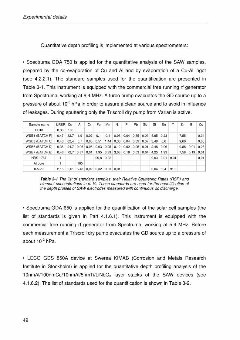
Experimental details
49
Quantitative depth profiling is implemented at various spectrometers:
• Spectruma GDA 750 is applied for the quantitative analysis of the SAW samples,
prepared by the co-evaporation of Cu and Al and by evaporation of a Cu-Al ingot
(see 4.2.2.1). The standard samples used for the quantification are presented in
Table 3-1. This instrument is equipped with the commercial free running rf generator
from Spectruma, working at 6,4 MHz. A turbo pump evacuates the GD source up to a
pressure of about 10-5 hPa in order to assure a clean source and to avoid in influence
of leakages. During sputtering only the Triscroll dry pump from Varian is active.
Sample name 1/RSR Cu Al Cr Fe Mn Ni P Pb Sb Si Sn Ti Zn Bi Co
CU10 0,35 100
WSB1 (BATCH F) 0,47 82,7 1,9 0,02 0,1 0,1 0,08 0,04 0,55 0,03 5,95 0,23 7,55 0,34
WSB3 (BATCH C) 0,46 82,4 0,7 0,05 0,51 1,44 0,36 0,04 0,39 0,07 3,48 0,6 9,66 0,05
WSB6 (BATCH D) 0,36 94,7 0,06 0,06 0,03 0,25 0,12 0,02 0,95 0,01 2,48 0,06 0,88 0,01 0,25
WSB7 (BATCH B) 0,46 72,7 3,87 0,01 1,95 3,39 3,03 0,19 0,03 0,64 4,25 1,93 7,58 0,19 0,01
NBS-1767 1 99,8 0,02 0,03 0,01 0,01 0,01
Al pure 1 100
TI-5-2-5 2,15 0,01 5,48 0,02 0,32 0,03 0,01 0,04 2,4 91,6
Table 3-1 The list of standard samples, their Relative Sputtering Rates (RSR) and element concentrations in m %. These standards are used for the quantification of the depth profiles of SAW electrodes measured with continuous dc discharge.
• Spectruma GDA 650 is applied for the quantification of the solar cell samples (the
list of standards is given in Part 4.1.6.1). This instrument is equipped with the
commercial free running rf generator from Spectruma, working at 5,9 MHz. Before
each measurement a Triscroll dry pump evacuates the GD source up to a pressure of
about 10-2 hPa.
• LECO GDS 850A device at Swerea KIMAB (Corrosion and Metals Research
Institute in Stockholm) is applied for the quantitative depth profiling analysis of the
10nmAl/100nmCu/10nmAl/5nmTi/LiNbO3 layer stacks of the SAW devices (see
4.1.6.2). The list of standards used for the quantification is shown in Table 3-2.
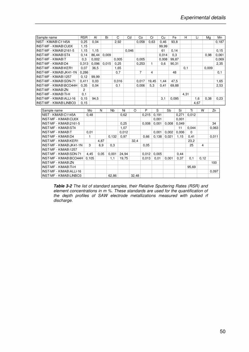
Experimental details
50
Sample name RSR Al Bi C Cd Co Cr Cu Fe H Li Mg MnNIST - KIMAB\C1145A 0,25 0,04 2,92 0,058 0,63 0,46 93,8 0,187INST-MF - KIMAB\CU0X 1,15 99,99INST-MF - KIMAB\2161-5 1,15 1,15 0,046 61 0,14 0,15INST-MF - KIMAB\ST4 0,14 86,44 0,009 0,014 0,3 0,98 0,061INST-MF - KIMAB\T 0,3 0,002 0,005 0,005 0,008 99,87 0,069INST-MF - KIMAB\D4 0,313 0,096 0,015 0,25 0,253 1 0,6 90,31 2,35INST-MF - KIMAB\KER1 0,07 36,5 1,65 0,1 0,009INST-MF - KIMAB\JK41-1N 0,286 0,7 7 4 48 0,1INST-MF - KIMAB\1257 0,12 99,99INST-MF - KIMAB\SDN-71 0,411 0,03 0,016 0,017 19,45 1,44 47,5 1,65INST-MF - KIMAB\BCO44H 0,35 0,04 0,1 0,006 5,3 0,41 69,88 2,53INST-MF - KIMAB\ZN 2INST-MF - KIMAB\TI-H 0,1 4,31INST-MF - KIMAB\ALLI-16 0,15 94,5 3,1 0,095 1,6 0,38 0,23INST-MF - KIMAB\LINBO3 0,15 4,67
Sample name Mo N Nb Ni O P S Sb Si Ti W ZnNIST - KIMAB\C1145A 0,48 0,62 0,215 0,191 0,271 0,012INST-MF - KIMAB\CU0X 0,001 0,001INST-MF - KIMAB\2161-5 0,25 0,008 0,001 0,008 0,049 34INST-MF - KIMAB\ST4 1,07 11 0,044 0,063INST-MF - KIMAB\T 0,01 0,012 0,001 0,002 0,006 0INST-MF - KIMAB\D4 1 0,132 0,97 0,66 0,138 0,021 1,15 0,41 0,011INST-MF - KIMAB\KER1 4,87 32,4 23,2INST-MF - KIMAB\JK41-1N 3 6,9 0,3 0,05 25 4INST-MF - KIMAB\1257INST-MF - KIMAB\SDN-71 4,45 0,05 0,001 24,94 0,012 0,005 0,44INST-MF - KIMAB\BCO44H 0,105 1,1 19,75 0,013 0,01 0,001 0,37 0,1 0,12INST-MF - KIMAB\ZN 100INST-MF - KIMAB\TI-H 95,69INST-MF - KIMAB\ALLI-16 0,097INST-MF - KIMAB\LINBO3 62,86 32,48
Table 3-2 The list of standard samples, their Relative Sputtering Rates (RSR) and element concentrations in m %. These standards are used for the quantification of the depth profiles of SAW electrode metallizations measured with pulsed rf discharge.
51
4 Results and discussion
4.1 Study of pulsed glow discharge
4.1.1 Defining the range of the PGD parameters
The parameters of PGD can be varied within a wide range providing either weak or
strong plasma with µs or ms pulse length. Therefore for the particular application it is
reasonable to select some narrow parameter ranges which favour reliable analysis
results. In the present work the studies are oriented to the analysis of layered and
thermally fragile samples. Therefore the main criteria for the selection of the
parameter ranges are: flat sputtered crater, moderate sputtering rates and minimal
thermal stress.
Voltage, current and pressure ranges In the introduction it was already mentioned
that the parameters of PGD are: voltage (U), current (I), pressure (p), duty cycle,
pulse length and frequency (see 2.3.1). The first three are fairly investigated for
continuous discharge. It is well known that U, I and p are not separately variable and
one can not change one of the parameters keeping two other immutable. But it was
found out that the pressure is a less important parameter for GD-OES.21,59 Also the
main sputtering equation of Boumans contains only U and I, which means that U and
I are the most convenient parameters to describe GD sputtering.62 If one assumes
that U and I have the greatest impact also for the pulsed discharge, the task of
defining the U, I and p ranges for PGD is simplified to only U and I.
For all analytical applications of the Grimm-type source, the GD is operated in
abnormal mode, where the sputtering is most stable and homogeneous. In this mode
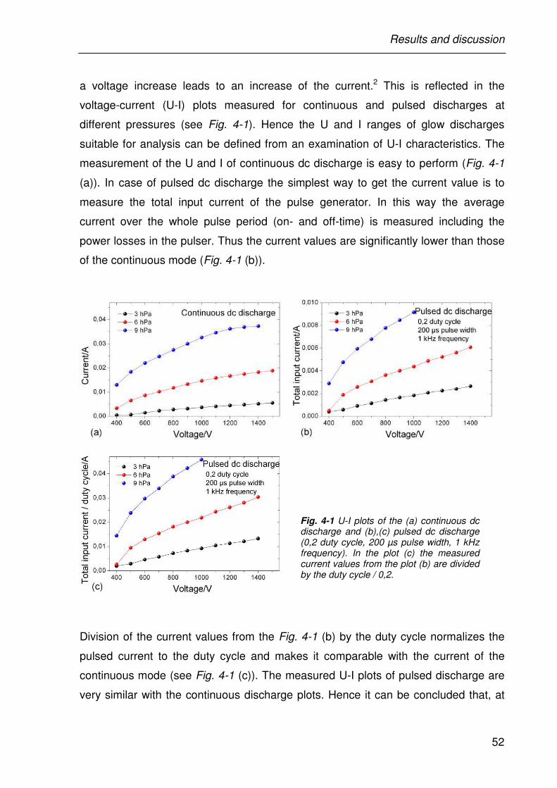
Results and discussion
52
a voltage increase leads to an increase of the current.2 This is reflected in the
voltage-current (U-I) plots measured for continuous and pulsed discharges at
different pressures (see Fig. 4-1). Hence the U and I ranges of glow discharges
suitable for analysis can be defined from an examination of U-I characteristics. The
measurement of the U and I of continuous dc discharge is easy to perform (Fig. 4-1
(a)). In case of pulsed dc discharge the simplest way to get the current value is to
measure the total input current of the pulse generator. In this way the average
current over the whole pulse period (on- and off-time) is measured including the
power losses in the pulser. Thus the current values are significantly lower than those
of the continuous mode (Fig. 4-1 (b)).
Fig. 4-1 U-I plots of the (a) continuous dc discharge and (b),(c) pulsed dc discharge (0,2 duty cycle, 200 µs pulse width, 1 kHz frequency). In the plot (c) the measured current values from the plot (b) are divided by the duty cycle / 0,2.
Division of the current values from the Fig. 4-1 (b) by the duty cycle normalizes the
pulsed current to the duty cycle and makes it comparable with the current of the
continuous mode (see Fig. 4-1 (c)). The measured U-I plots of pulsed discharge are
very similar with the continuous discharge plots. Hence it can be concluded that, at
Results and discussion
53
the same pressure range from 3-9 hPa, the voltage range of pulsed discharge, where
the U-I plots indicate the abnormal mode, is the same as in continuous discharge:
500 - 1400 V. It should be mentioned that the upper voltage limit for the pulsed
discharge can be higher and depends on the power supply. Nevertheless 1400 V
were chosen to be able to compare pulsed discharge with the continuous one,
because the maximum voltage of the continuous mode is limited to around 1400 V
due to the strong heating at high powers.
From the Fig 4-1 (a) and (c) can be seen that the slopes of the U-I plots of
continuous and pulsed discharges differ: U-I plots of the pulsed mode are steeper
than those of the continuous one. Also at high powers the U-I plots are more curved.
This important phenomenon is thoroughly analyzed in the following text and parts
4.1.2 and 4.1.3.1.
Measurement of the U-I plots of the pulsed rf discharge is even more complex
than for dc mode and will be discussed in the next parts. In this work the considered
voltage range for the pulsed rf discharge is the same as in dc mode – 400-1400 V.
The current range, similarly with voltage, can be deduced from the U-I plots.
For example for a 20 % duty cycle and 200 µs pulse length the total input current
values where observed to be from 1 to 7 mA. With these current values the U-I plot is
nearly linear, what indicates the abnormal mode. The corresponding pressure is
6 hPa. At commercial spectrometers or experimental setups in case of pulsed
discharge it is easier to measure pressure than current. Therefore, for most
experiments in this work the current is not recorded but the pressure is set to a value
close to 6 hPa.
Duty cycle, pulse length and frequency ranges The range of the pulse parameters
duty cycle, pulse length and frequency is not so often discussed as the electrical
parameters U, I and p. The applied frequencies can be from the Hz77 region to
several kHz,184 the pulse durations – from µs185 to ms.98,186 Correspondingly the duty
cycle may vary from 0 to 100 %. Studying the PGD within all these parameter ranges
can take a lot of time and makes no sense, because the analysis conditions of
layered or thermally fragile samples have limitations. It is worthwhile to determine
these limitations.
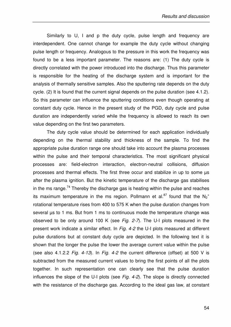
Results and discussion
54
Similarly to U, I and p the duty cycle, pulse length and frequency are
interdependent. One cannot change for example the duty cycle without changing
pulse length or frequency. Analogous to the pressure in this work the frequency was
found to be a less important parameter. The reasons are: (1) The duty cycle is
directly correlated with the power introduced into the discharge. Thus this parameter
is responsible for the heating of the discharge system and is important for the
analysis of thermally sensitive samples. Also the sputtering rate depends on the duty
cycle. (2) It is found that the current signal depends on the pulse duration (see 4.1.2).
So this parameter can influence the sputtering conditions even though operating at
constant duty cycle. Hence in the present study of the PGD, duty cycle and pulse
duration are independently varied while the frequency is allowed to reach its own
value depending on the first two parameters.
The duty cycle value should be determined for each application individually
depending on the thermal stability and thickness of the sample. To find the
appropriate pulse duration range one should take into account the plasma processes
within the pulse and their temporal characteristics. The most significant physical
processes are: field-electron interaction, electron-neutral collisions, diffusion
processes and thermal effects. The first three occur and stabilize in up to some µs
after the plasma ignition. But the kinetic temperature of the discharge gas stabilises
in the ms range.74 Thereby the discharge gas is heating within the pulse and reaches
its maximum temperature in the ms region. Pollmann et al.87 found that the N2+
rotational temperature rises from 400 to 575 K when the pulse duration changes from
several µs to 1 ms. But from 1 ms to continuous mode the temperature change was
observed to be only around 100 K (see Fig. 2-7). The U-I plots measured in the
present work indicate a similar effect. In Fig. 4-2 the U-I plots measured at different
pulse durations but at constant duty cycle are depicted. In the following text it is
shown that the longer the pulse the lower the average current value within the pulse
(see also 4.1.2.2 Fig. 4-13). In Fig. 4-2 the current difference (offset) at 500 V is
subtracted from the measured current values to bring the first points of all the plots
together. In such representation one can clearly see that the pulse duration
influences the slope of the U-I plots (see Fig. 4-2). The slope is directly connected
with the resistance of the discharge gas. According to the ideal gas law, at constant
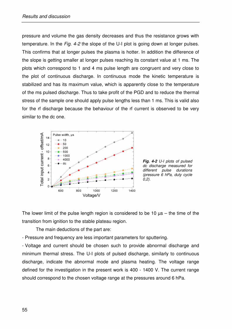
Results and discussion
55
pressure and volume the gas density decreases and thus the resistance grows with
temperature. In the Fig. 4-2 the slope of the U-I plot is going down at longer pulses.
This confirms that at longer pulses the plasma is hotter. In addition the difference of
the slope is getting smaller at longer pulses reaching its constant value at 1 ms. The
plots which correspond to 1 and 4 ms pulse length are congruent and very close to
the plot of continuous discharge. In continuous mode the kinetic temperature is
stabilized and has its maximum value, which is apparently close to the temperature
of the ms pulsed discharge. Thus to take profit of the PGD and to reduce the thermal
stress of the sample one should apply pulse lengths less than 1 ms. This is valid also
for the rf discharge because the behaviour of the rf current is observed to be very
similar to the dc one.
Fig. 4-2 U-I plots of pulsed dc discharge measured for different pulse durations (pressure 6 hPa, duty cycle 0,2).
The lower limit of the pulse length region is considered to be 10 µs – the time of the
transition from ignition to the stable plateau region.
The main deductions of the part are:
- Pressure and frequency are less important parameters for sputtering.
- Voltage and current should be chosen such to provide abnormal discharge and
minimum thermal stress. The U-I plots of pulsed discharge, similarly to continuous
discharge, indicate the abnormal mode and plasma heating. The voltage range
defined for the investigation in the present work is 400 - 1400 V. The current range
should correspond to the chosen voltage range at the pressures around 6 hPa.
Results and discussion
56
- The duty cycle should be determined individually for each sample. The application
of pulses longer than 1 ms causes a discharge gas heating close to that of the
continuous discharge. The pulse length range defined for the study is 10 – 1000 µs.
4.1.2 Electrical properties of PGD
One of the keys to understand the glow discharge is its electrical behaviour. The
electrical properties, in particular the U–I characteristics, current and voltage signal
shapes within the pulse, are important for the understanding of the processes taking
place in the glow discharge. Electrical properties are also closely related to the
analytical performance of PGD, due to their effect on the sputtering rates, sputtered
crater shapes and emission yields. 51,187-195 In addition in the previous part (see 4.1.1)
it was shown, that the voltage–current plots indicate whether the discharge is
operating in the abnormal mode, which is extremely important for homogeneous
sample sputtering and efficient excitation and ionization. Electrical parameters of the
discharge are also necessary for the plasma modelling studies.196,197 Nevertheless in
case of PGD there is a lack of studies where the current and voltage signals are
considered in detail. Even though the influence of the pulse parameters on the crater
shape78 and emission intensity198-200 is considered, less attention is paid on the
electrical properties of the PGD. Therefore, in this dissertation the 4.1.2 part is
dedicated to the electrical properties of PGD. The influence of the PGD parameters
(duty cycle and pulse duration) on the electrical properties is examined. The pulse
frequency is not considered because it is the less important parameter (see above
section 4.1.1) and is allowed to reach its own value depending on the duty cycle and
pulse duration.
In the introduction the question, whether dc and rf discharges behave similarly
is brought up (see 2.3.2). This question is actual till nowadays and for the PGD it is
even less studied. Therefore in this work the comparative studies of the electrical
properties of the dc and rf pulsed discharges are made. Nearly all experiments are
performed for both dc and rf pulsed discharges, keeping in mind that the effective
voltage should be used in the case of an rf discharge in order to obtain the same
plasma conditions as in dc mode.
Results and discussion
57
4.1.2.1 Voltage-current plots of PGD
The importance of the abnormal discharge mode for the analytical applications has
been already discussed in the introduction and in the previous section. In this mode
the discharge conditions are selected such that the current flows homogeneously
through the cathode surface thus providing flat craters and high power. The
expansion of the plasma over the cathode is obstructed by the anode. Therefore, at
higher voltages more electrons are extracted from the surface per unit area and the
current increases. This process defines the form of the U–I characteristics of the GD:
the current increases with voltage. The U-I plots of the PGD are found to resemble
the U-I plots of the continuous discharge (see Fig. 4-1). However whereas for the
continuous dc mode the measurement of the U-I plots is experimentally simple and
straightforward, for the pulsed mode there are several measurement options. It is
essential to choose a convenient type of current signal acquisition. This acquisition is
also different for the dc and rf pulses. Therefore in the following text the
measurement of the U-I plots of pulsed dc and rf discharges will be sequentially
described.
Dc pulsed discharge With the high voltage dc pulse generator RUP 3-3a, applied in
this work, there are two possibilities to record the current signal. One of them
provides a high time resolved measurement of the current within the pulse. The other
gives the total input current of the pulser. So, for the voltage–current plots one can
either measure the current within the pulse and calculate the average value during
the pulse on-time (method 1) or measure the input current and divide it by the duty
cycle (method 2). The second method is used in the section 4.1.1 (see Fig. 4-1 and
Fig. 4-2). Both methods produce an averaged current value during one pulse.
Experiments have shown that the current measured by method 2 exceeds the current
from the method 1 by about 15% (see Fig. 4-3).
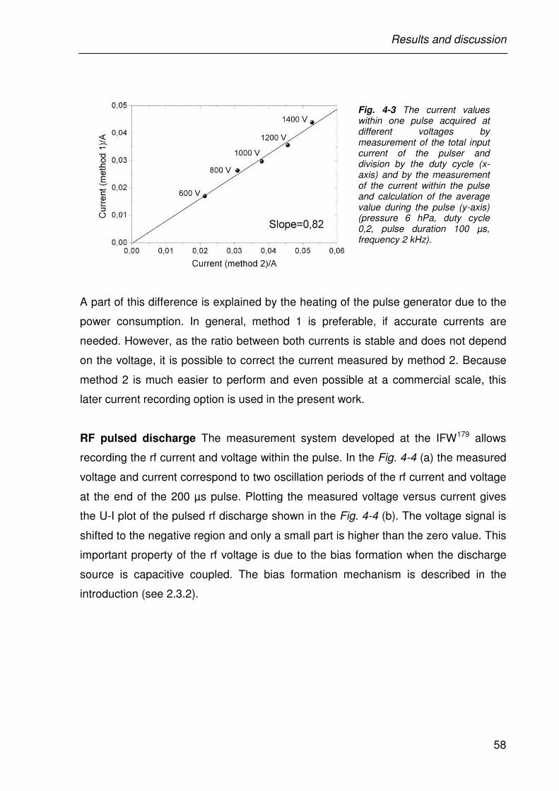
Results and discussion
58
Fig. 4-3 The current values within one pulse acquired at different voltages by measurement of the total input current of the pulser and division by the duty cycle (x-axis) and by the measurement of the current within the pulse and calculation of the average value during the pulse (y-axis) (pressure 6 hPa, duty cycle 0,2, pulse duration 100 µs, frequency 2 kHz).
A part of this difference is explained by the heating of the pulse generator due to the
power consumption. In general, method 1 is preferable, if accurate currents are
needed. However, as the ratio between both currents is stable and does not depend
on the voltage, it is possible to correct the current measured by method 2. Because
method 2 is much easier to perform and even possible at a commercial scale, this
later current recording option is used in the present work.
RF pulsed discharge The measurement system developed at the IFW179 allows
recording the rf current and voltage within the pulse. In the Fig. 4-4 (a) the measured
voltage and current correspond to two oscillation periods of the rf current and voltage
at the end of the 200 µs pulse. Plotting the measured voltage versus current gives
the U-I plot of the pulsed rf discharge shown in the Fig. 4-4 (b). The voltage signal is
shifted to the negative region and only a small part is higher than the zero value. This
important property of the rf voltage is due to the bias formation when the discharge
source is capacitive coupled. The bias formation mechanism is described in the
introduction (see 2.3.2).
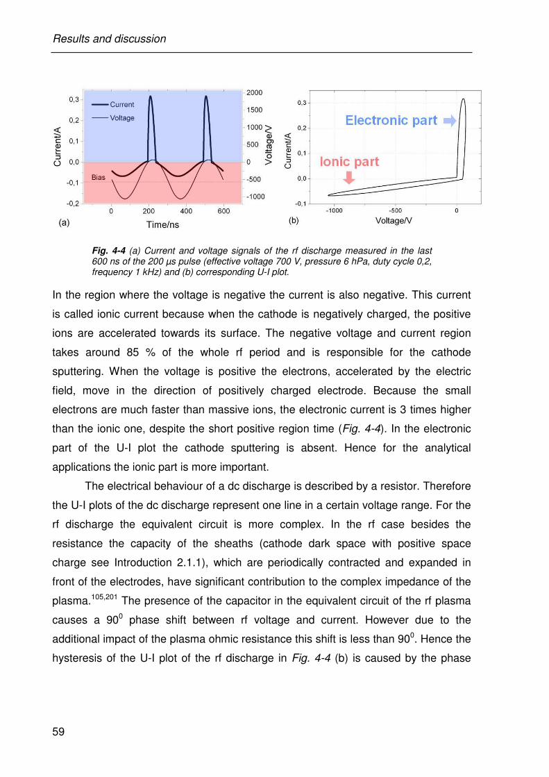
Results and discussion
59
Fig. 4-4 (a) Current and voltage signals of the rf discharge measured in the last 600 ns of the 200 µs pulse (effective voltage 700 V, pressure 6 hPa, duty cycle 0,2, frequency 1 kHz) and (b) corresponding U-I plot.
In the region where the voltage is negative the current is also negative. This current
is called ionic current because when the cathode is negatively charged, the positive
ions are accelerated towards its surface. The negative voltage and current region
takes around 85 % of the whole rf period and is responsible for the cathode
sputtering. When the voltage is positive the electrons, accelerated by the electric
field, move in the direction of positively charged electrode. Because the small
electrons are much faster than massive ions, the electronic current is 3 times higher
than the ionic one, despite the short positive region time (Fig. 4-4). In the electronic
part of the U-I plot the cathode sputtering is absent. Hence for the analytical
applications the ionic part is more important.
The electrical behaviour of a dc discharge is described by a resistor. Therefore
the U-I plots of the dc discharge represent one line in a certain voltage range. For the
rf discharge the equivalent circuit is more complex. In the rf case besides the
resistance the capacity of the sheaths (cathode dark space with positive space
charge see Introduction 2.1.1), which are periodically contracted and expanded in
front of the electrodes, have significant contribution to the complex impedance of the
plasma.105,201 The presence of the capacitor in the equivalent circuit of the rf plasma
causes a 900 phase shift between rf voltage and current. However due to the
additional impact of the plasma ohmic resistance this shift is less than 900. Hence the
hysteresis of the U-I plot of the rf discharge in Fig. 4-4 (b) is caused by the phase
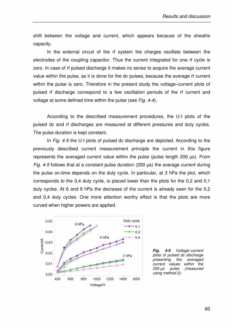
Results and discussion
60
shift between the voltage and current, which appears because of the sheaths
capacity.
In the external circuit of the rf system the charges oscillate between the
electrodes of the coupling capacitor. Thus the current integrated for one rf cycle is
zero. In case of rf pulsed discharge it makes no sense to acquire the average current
value within the pulse, as it is done for the dc pulses, because the average rf current
within the pulse is zero. Therefore in the present study the voltage–current plots of
pulsed rf discharge correspond to a few oscillation periods of the rf current and
voltage at some defined time within the pulse (see Fig. 4-4).
According to the described measurement procedures, the U-I plots of the
pulsed dc and rf discharges are measured at different pressures and duty cycles.
The pulse duration is kept constant.
In Fig. 4-5 the U-I plots of pulsed dc discharge are depicted. According to the
previously described current measurement principle the current in this figure
represents the averaged current value within the pulse (pulse length 200 µs). From
Fig. 4-5 follows that at a constant pulse duration (200 µs) the average current during
the pulse on-time depends on the duty cycle. In particular, at 3 hPa the plot, which
corresponds to the 0,4 duty cycle, is placed lower than the plots for the 0,2 and 0,1
duty cycles. At 6 and 9 hPa the decrease of the current is already seen for the 0,2
and 0,4 duty cycles. One more attention worthy effect is that the plots are more
curved when higher powers are applied.
Fig. 4-5 Voltage–current plots of pulsed dc discharge presenting the averaged current values within the 200 µs pulse (measured using method 2).
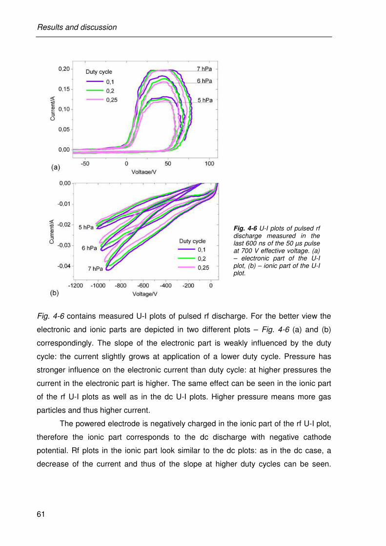
Results and discussion
61
Fig. 4-6 U-I plots of pulsed rf discharge measured in the last 600 ns of the 50 µs pulse at 700 V effective voltage. (a) – electronic part of the U-I plot, (b) – ionic part of the U-I plot.
Fig. 4-6 contains measured U-I plots of pulsed rf discharge. For the better view the
electronic and ionic parts are depicted in two different plots – Fig. 4-6 (a) and (b)
correspondingly. The slope of the electronic part is weakly influenced by the duty
cycle: the current slightly grows at application of a lower duty cycle. Pressure has
stronger influence on the electronic current than duty cycle: at higher pressures the
current in the electronic part is higher. The same effect can be seen in the ionic part
of the rf U-I plots as well as in the dc U-I plots. Higher pressure means more gas
particles and thus higher current.
The powered electrode is negatively charged in the ionic part of the rf U-I plot,
therefore the ionic part corresponds to the dc discharge with negative cathode
potential. Rf plots in the ionic part look similar to the dc plots: as in the dc case, a
decrease of the current and thus of the slope at higher duty cycles can be seen.
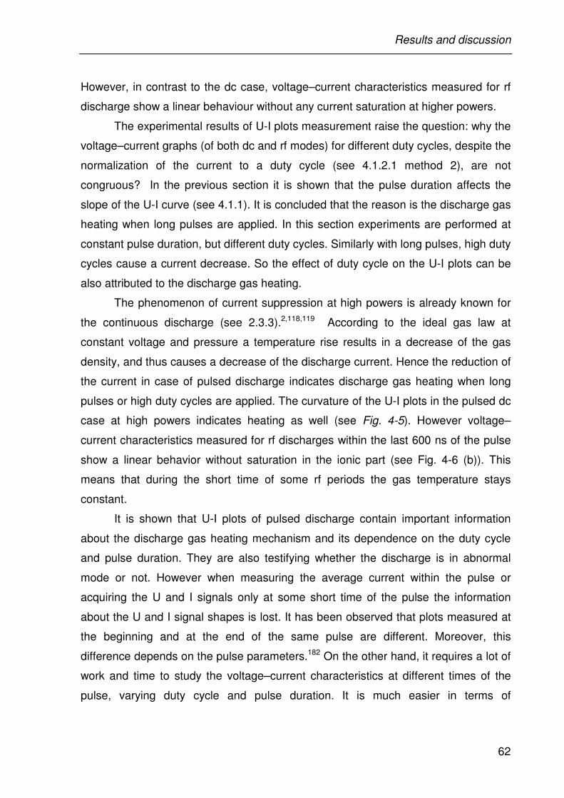
Results and discussion
62
However, in contrast to the dc case, voltage–current characteristics measured for rf
discharge show a linear behaviour without any current saturation at higher powers.
The experimental results of U-I plots measurement raise the question: why the
voltage–current graphs (of both dc and rf modes) for different duty cycles, despite the
normalization of the current to a duty cycle (see 4.1.2.1 method 2), are not
congruous? In the previous section it is shown that the pulse duration affects the
slope of the U-I curve (see 4.1.1). It is concluded that the reason is the discharge gas
heating when long pulses are applied. In this section experiments are performed at
constant pulse duration, but different duty cycles. Similarly with long pulses, high duty
cycles cause a current decrease. So the effect of duty cycle on the U-I plots can be
also attributed to the discharge gas heating.
The phenomenon of current suppression at high powers is already known for
the continuous discharge (see 2.3.3).2,118,119 According to the ideal gas law at
constant voltage and pressure a temperature rise results in a decrease of the gas
density, and thus causes a decrease of the discharge current. Hence the reduction of
the current in case of pulsed discharge indicates discharge gas heating when long
pulses or high duty cycles are applied. The curvature of the U-I plots in the pulsed dc
case at high powers indicates heating as well (see Fig. 4-5). However voltage–
current characteristics measured for rf discharges within the last 600 ns of the pulse
show a linear behavior without saturation in the ionic part (see Fig. 4-6 (b)). This
means that during the short time of some rf periods the gas temperature stays
constant.
It is shown that U-I plots of pulsed discharge contain important information
about the discharge gas heating mechanism and its dependence on the duty cycle
and pulse duration. They are also testifying whether the discharge is in abnormal
mode or not. However when measuring the average current within the pulse or
acquiring the U and I signals only at some short time of the pulse the information
about the U and I signal shapes is lost. It has been observed that plots measured at
the beginning and at the end of the same pulse are different. Moreover, this
difference depends on the pulse parameters.182 On the other hand, it requires a lot of
work and time to study the voltage–current characteristics at different times of the
pulse, varying duty cycle and pulse duration. It is much easier in terms of
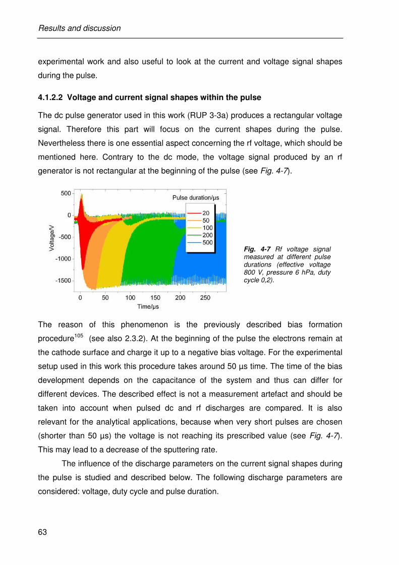
Results and discussion
63
experimental work and also useful to look at the current and voltage signal shapes
during the pulse.
4.1.2.2 Voltage and current signal shapes within the pulse
The dc pulse generator used in this work (RUP 3-3a) produces a rectangular voltage
signal. Therefore this part will focus on the current shapes during the pulse.
Nevertheless there is one essential aspect concerning the rf voltage, which should be
mentioned here. Contrary to the dc mode, the voltage signal produced by an rf
generator is not rectangular at the beginning of the pulse (see Fig. 4-7).
Fig. 4-7 Rf voltage signal measured at different pulse durations (effective voltage 800 V, pressure 6 hPa, duty cycle 0,2).
The reason of this phenomenon is the previously described bias formation
procedure105 (see also 2.3.2). At the beginning of the pulse the electrons remain at
the cathode surface and charge it up to a negative bias voltage. For the experimental
setup used in this work this procedure takes around 50 µs time. The time of the bias
development depends on the capacitance of the system and thus can differ for
different devices. The described effect is not a measurement artefact and should be
taken into account when pulsed dc and rf discharges are compared. It is also
relevant for the analytical applications, because when very short pulses are chosen
(shorter than 50 µs) the voltage is not reaching its prescribed value (see Fig. 4-7).
This may lead to a decrease of the sputtering rate.
The influence of the discharge parameters on the current signal shapes during
the pulse is studied and described below. The following discharge parameters are
considered: voltage, duty cycle and pulse duration.
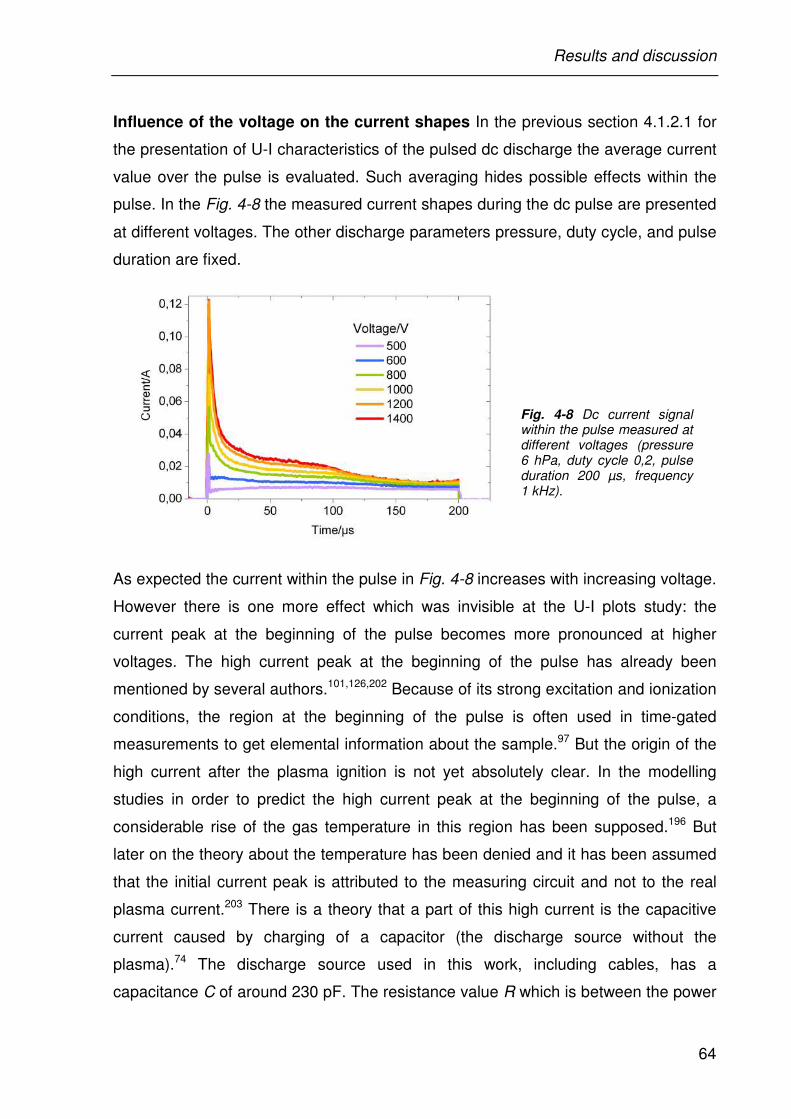
Results and discussion
64
Influence of the voltage on the current shapes In the previous section 4.1.2.1 for
the presentation of U-I characteristics of the pulsed dc discharge the average current
value over the pulse is evaluated. Such averaging hides possible effects within the
pulse. In the Fig. 4-8 the measured current shapes during the dc pulse are presented
at different voltages. The other discharge parameters pressure, duty cycle, and pulse
duration are fixed.
Fig. 4-8 Dc current signal within the pulse measured at different voltages (pressure 6 hPa, duty cycle 0,2, pulse duration 200 µs, frequency 1 kHz).
As expected the current within the pulse in Fig. 4-8 increases with increasing voltage.
However there is one more effect which was invisible at the U-I plots study: the
current peak at the beginning of the pulse becomes more pronounced at higher
voltages. The high current peak at the beginning of the pulse has already been
mentioned by several authors.101,126,202 Because of its strong excitation and ionization
conditions, the region at the beginning of the pulse is often used in time-gated
measurements to get elemental information about the sample.97 But the origin of the
high current after the plasma ignition is not yet absolutely clear. In the modelling
studies in order to predict the high current peak at the beginning of the pulse, a
considerable rise of the gas temperature in this region has been supposed.196 But
later on the theory about the temperature has been denied and it has been assumed
that the initial current peak is attributed to the measuring circuit and not to the real
plasma current.203 There is a theory that a part of this high current is the capacitive
current caused by charging of a capacitor (the discharge source without the
plasma).74 The discharge source used in this work, including cables, has a
capacitance C of around 230 pF. The resistance value R which is between the power
Results and discussion
65
supply and the source is 35 Ohm. So in this case the application of a voltage U0 (for
example 800 V) across the 230 pF capacitor will really produce a huge current peak
Imax of several Ampere, but it will decay in some ns (see Fig. 4-9).
Fig. 4-9 Simplified equivalent circuit of the dc discharge system (which includes the dc power generator, the resistance of the generator and the cables and the source capacity) and calculation of the corresponding capacitor charging time.
The huge peak of 22,9 A in the first ns of the pulse is very likely existing, but it is not
possible to record it with the equipment used in the present study (the applied
voltage probes are not made for such high frequency and current). Thereby the
assumption about the capacitive current doesn’t explain the often observed current
peak in the µs region, like in the Fig. 4-8. Therefore further work, especially
computational studies on this topic are necessary.
Compression of the time scale of the measured rf current signal from the Fig.
4-4 (a) gives the rf current shape within the pulse. In this way the rf current signal
shapes at different effective voltages, but constant duty cycle and pulse duration are
measured (see Fig. 4-10). It is interesting that the behaviour of the pulsed rf
discharge is rather like in the dc case (see Fig. 4-8) and current peaks appear in the
prepeak region as well in the both electronic (positive) and ionic (negative) parts. In
comparison with the plateau region the current peak at the beginning of the rf pulse is
not so high as in dc case. But one can clearly see the similarity between rf and dc
pulses: the peaks disappear at lower voltages.
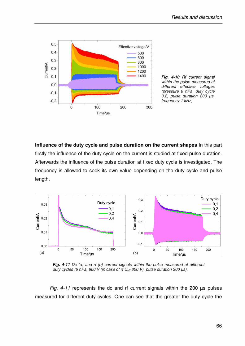
Results and discussion
66
Fig. 4-10 Rf current signal within the pulse measured at different effective voltages (pressure 6 hPa, duty cycle 0,2, pulse duration 200 µs, frequency 1 kHz).
Influence of the duty cycle and pulse duration on the current shapes In this part
firstly the influence of the duty cycle on the current is studied at fixed pulse duration.
Afterwards the influence of the pulse duration at fixed duty cycle is investigated. The
frequency is allowed to seek its own value depending on the duty cycle and pulse
length.
Fig. 4-11 Dc (a) and rf (b) current signals within the pulse measured at different duty cycles (6 hPa, 800 V (in case of rf Ueff 800 V), pulse duration 200 µs).
Fig. 4-11 represents the dc and rf current signals within the 200 µs pulses
measured for different duty cycles. One can see that the greater the duty cycle the
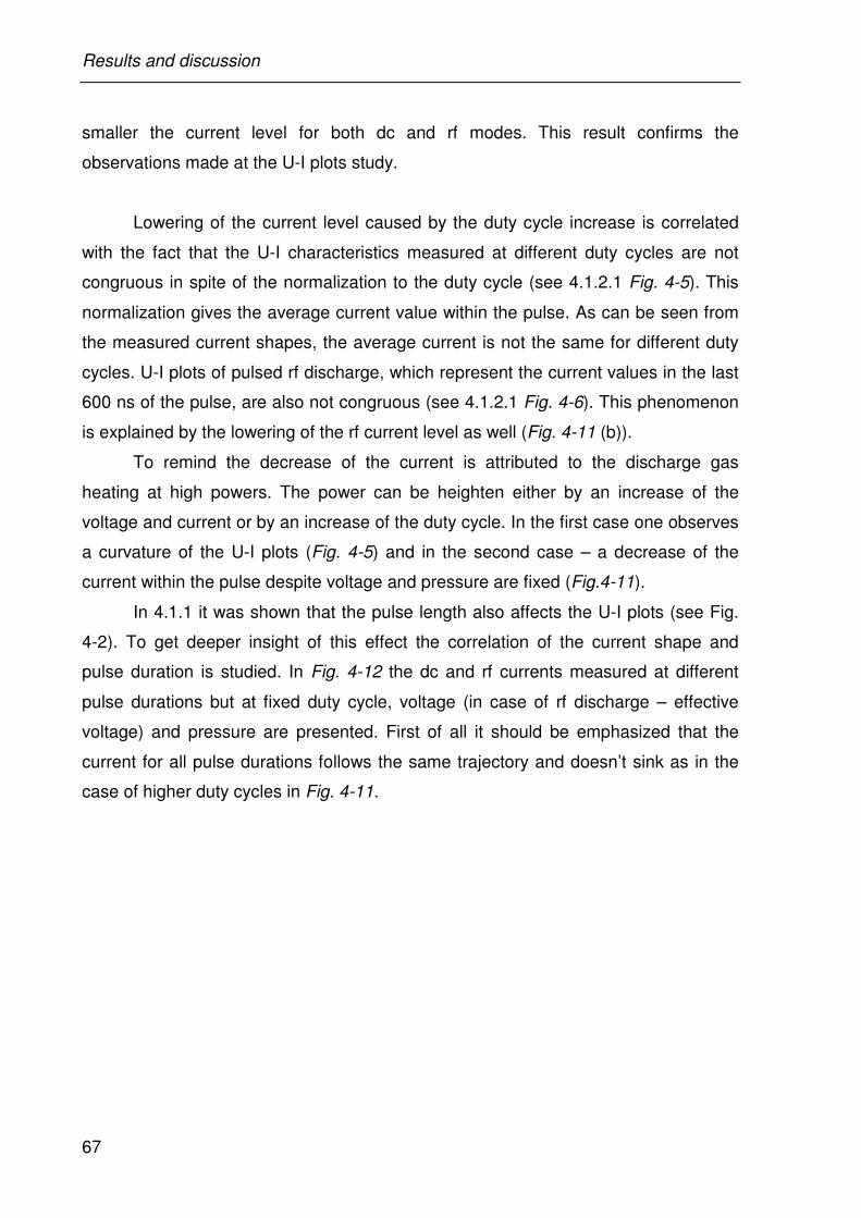
Results and discussion
67
smaller the current level for both dc and rf modes. This result confirms the
observations made at the U-I plots study.
Lowering of the current level caused by the duty cycle increase is correlated
with the fact that the U-I characteristics measured at different duty cycles are not
congruous in spite of the normalization to the duty cycle (see 4.1.2.1 Fig. 4-5). This
normalization gives the average current value within the pulse. As can be seen from
the measured current shapes, the average current is not the same for different duty
cycles. U-I plots of pulsed rf discharge, which represent the current values in the last
600 ns of the pulse, are also not congruous (see 4.1.2.1 Fig. 4-6). This phenomenon
is explained by the lowering of the rf current level as well (Fig. 4-11 (b)).
To remind the decrease of the current is attributed to the discharge gas
heating at high powers. The power can be heighten either by an increase of the
voltage and current or by an increase of the duty cycle. In the first case one observes
a curvature of the U-I plots (Fig. 4-5) and in the second case – a decrease of the
current within the pulse despite voltage and pressure are fixed (Fig.4-11).
In 4.1.1 it was shown that the pulse length also affects the U-I plots (see Fig.
4-2). To get deeper insight of this effect the correlation of the current shape and
pulse duration is studied. In Fig. 4-12 the dc and rf currents measured at different
pulse durations but at fixed duty cycle, voltage (in case of rf discharge – effective
voltage) and pressure are presented. First of all it should be emphasized that the
current for all pulse durations follows the same trajectory and doesn’t sink as in the
case of higher duty cycles in Fig. 4-11.
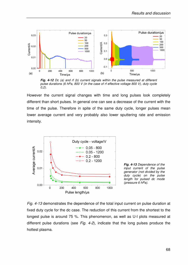
Results and discussion
68
Fig. 4-12 Dc (a) and rf (b) current signals within the pulse measured at different pulse durations (6 hPa, 800 V (in the case of rf effective voltage 800 V), duty cycle 0,2).
However the current signal changes with time and long pulses look completely
different than short pulses. In general one can see a decrease of the current with the
time of the pulse. Therefore in spite of the same duty cycle, longer pulses mean
lower average current and very probably also lower sputtering rate and emission
intensity.
Fig. 4-13 Dependence of the input current of the pulse generator (not divided by the duty cycle) on the pulse length for pulsed dc mode (pressure 6 hPa).
Fig. 4-13 demonstrates the dependence of the total input current on pulse duration at
fixed duty cycle for the dc case. The reduction of this current from the shortest to the
longest pulse is around 75 %. This phenomenon, as well as U-I plots measured at
different pulse durations (see Fig. 4-2), indicate that the long pulses produce the
hottest plasma.
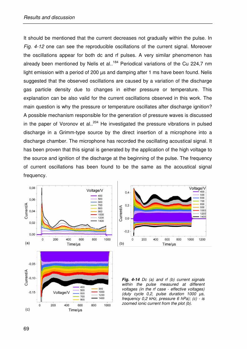
Results and discussion
69
It should be mentioned that the current decreases not gradually within the pulse. In
Fig. 4-12 one can see the reproducible oscillations of the current signal. Moreover
the oscillations appear for both dc and rf pulses. A very similar phenomenon has
already been mentioned by Nelis et al..184 Periodical variations of the Cu 224,7 nm
light emission with a period of 200 µs and damping after 1 ms have been found. Nelis
suggested that the observed oscillations are caused by a variation of the discharge
gas particle density due to changes in either pressure or temperature. This
explanation can be also valid for the current oscillations observed in this work. The
main question is why the pressure or temperature oscillates after discharge ignition?
A possible mechanism responsible for the generation of pressure waves is discussed
in the paper of Voronov et al..204 He investigated the pressure vibrations in pulsed
discharge in a Grimm-type source by the direct insertion of a microphone into a
discharge chamber. The microphone has recorded the oscillating acoustical signal. It
has been proven that this signal is generated by the application of the high voltage to
the source and ignition of the discharge at the beginning of the pulse. The frequency
of current oscillations has been found to be the same as the acoustical signal
frequency.
Fig. 4-14 Dc (a) and rf (b) current signals within the pulse measured at different voltages (in the rf case - effective voltages) (duty cycle 0,2, pulse duration 1000 µs, frequency 0,2 kHz, pressure 6 hPa); (c) - is zoomed ionic current from the plot (b).
Results and discussion
70
Observation of Voronov et al.204 can likely be an explanation of the current
oscillations found in this work for both dc and rf discharges. If a sharp voltage rise
induces the pressure waves in the discharge chamber, the oscillations should
disappear at lower voltages. This supposition is confirmed by the experimental
results in Fig. 4-14: oscillations, as well as the current peak at the leading age of the
pulse, are going down at lower voltages. In the rf case the pressure waves are
expected to affect both ionic and electronic current, which is also confirmed by the
experiment: electronic and ionic current show symmetrical oscillations (see Fig. 4-14
(b) and (c)).
In summary, part 4.1.2 covers the electrical features of the PGD which are crucial for
both understanding of the discharge processes and analytical applications.
Nearly all phenomena found for the dc discharge also appeared in the rf case.
No significant difference between rf and dc pulsed discharges have been found. The
current signal shape within the pulse has shown a similar behaviour in the rf and dc
modes: (1) growth of a current peak at the beginning of the pulse at higher voltages,
(2) sinking of the current level within the pulse when a higher duty cycle is applied
and (3) oscillations of the current signal within long (up to 1 ms) pulses. Thereby in
terms of the electrical properties the pulsed rf and dc discharges are very similar.
It has been found, that the current signal is not constant during the pulse. Thus
the pulse duration is an important parameter. The experimental results have shown
that at fixed duty cycle the average discharge current depends on the pulse duration.
The shorter is the dc pulse the higher is the average current. Presumably, the
sputtering rate and emission intensity are also influenced by the pulse length, in spite
of the fixed duty cycle. An important feature of the rf mode is that the rf voltage needs
around 50 µs to reach its prescribed value because of the bias formation. So the
choice of very short pulses can cause a decrease of the sputtering rate. The detailed
investigation of the sputtering rates and the emission intensities of the PGD
considering the results of the electrical properties is described in the parts 4.1.4 and
4.1.5.
For both, rf and dc discharges, a decrease of the current caused by a heating
of the discharge gas at higher powers has been observed. This effect provoked an
Results and discussion
71
idea of estimation of the discharge gas temperature from the U-I plots of PGD, which
is described in the next part (4.1.3.1).
4.1.3 Measurements of the PGD gas temperature
In 2.3.3 it is shown that knowledge of the discharge gas temperature is relevant for
the analysis of thermal fragile samples and for the fundamental studies as well. For
example the depth resolution and the sputtering rate depend on the temperature of
the sample and the discharge gas.80,81 Too high temperature can even partly melt82
or mechanically destroy the sample. The application of PGD allows reducing the
sample heating during the analysis and thereby promotes a good depth resolution. In
this part the reduction of the GD gas temperature at application of pulsed discharge
is estimated.
4.1.3.1 Voltage-current plots of the PGD as a thermometer for the GD gas
According to the previously made suggestion, the decrease of the current amplitude
with the duty cycle is due to the influence of discharge power on the temperature of
the gas. When the duty cycle increases the mean power consumption increases too.
This leads to a heating of the plasma gas. Under constant pressure according to the
thermodynamic law p=nkT an increase of the gas temperature leads to the decrease
of Ar atom concentration and therefore of the current. Processes like different
secondary electron emission yield at the sample surface caused by temperature
changes of the sample or changing concentration of the sputtered material in the
plasma are considered as less important.
The phenomenon of the current decrease at high powers gives an approach to
the estimation of the discharge gas temperature. The impedance of the plasma
depends strongly on the Ar atom concentration. But the concentration at low
temperature and low pressure corresponds to the same concentration at certain
higher temperatures and higher pressures: phigh/Thigh=plow/Tlow. In this equation plow
can be assumed to correspond to the discharge gas with the room temperature Tlow.
phigh is the pressure of the hot discharge gas with unknown temperature Thigh. phigh
and plow are easy measurable. Thus the only unknown value is Thigh which is deduced
from the: phigh/Thigh=plow/Tlow. In Fig. 4-15 the temperature estimation principle is
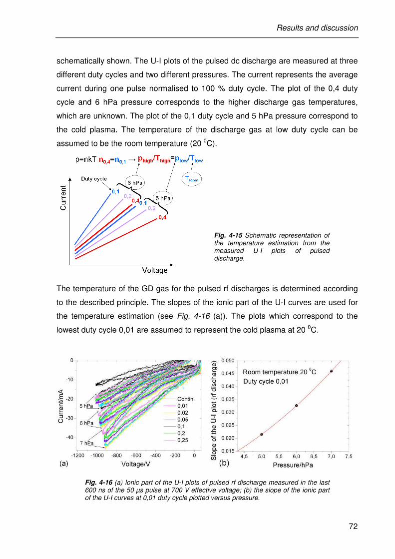
Results and discussion
72
schematically shown. The U-I plots of the pulsed dc discharge are measured at three
different duty cycles and two different pressures. The current represents the average
current during one pulse normalised to 100 % duty cycle. The plot of the 0,4 duty
cycle and 6 hPa pressure corresponds to the higher discharge gas temperatures,
which are unknown. The plot of the 0,1 duty cycle and 5 hPa pressure correspond to
the cold plasma. The temperature of the discharge gas at low duty cycle can be
assumed to be the room temperature (20 0C).
Fig. 4-15 Schematic representation of the temperature estimation from the measured U-I plots of pulsed discharge.
The temperature of the GD gas for the pulsed rf discharges is determined according
to the described principle. The slopes of the ionic part of the U-I curves are used for
the temperature estimation (see Fig. 4-16 (a)). The plots which correspond to the
lowest duty cycle 0,01 are assumed to represent the cold plasma at 20 0C.
Fig. 4-16 (a) Ionic part of the U-I plots of pulsed rf discharge measured in the last 600 ns of the 50 µs pulse at 700 V effective voltage; (b) the slope of the ionic part of the U-I curves at 0,01 duty cycle plotted versus pressure.
Results and discussion
73
To simplify the determination of plow, the dependence of the U-I slope on pressure at
room temperature (0,01 duty cycle) is plotted (see Fig. 4-16 (b)). From this plot plow is
determined for each U-I plot at duty cycles higher than 0,01. Further, with known
phigh, plow and Tlow the temperature Thigh is calculated using equation:
phigh/Thigh=plow/Tlow.
In case of pulsed dc discharge the U-I plots are measured for the same
pressures and duty cycles as for rf mode (see Fig. 4-17 (a)), using method 2
described in 4.1.2.1. However the temperature estimation from the slope of these
plots makes no sense because each point of the U-I plots corresponds to a different
power and therefore to a different temperature. To remind, the U-I plots of the rf
discharge are measured in the last 600 ns of the 50 µs pulse at constant effective
voltage (700 V). As already said in part 4.1.2.1, the U–I characteristics measured for
rf discharges within the last 600 ns of the pulse show a linear behavior without
saturation in the ionic part. This means that during the short time of some rf periods
the gas temperature stays constant. Hence the estimation of the discharge gas
temperature from the slope of the U-I plots is reliable for the rf discharge, but not for
the dc one.
To estimate the discharge gas temperature in case of pulsed dc discharge the
same principle as for rf mode is used, but instead of the slope just the current value
at 700 V is used. The 700 V voltage is taken for a better comparison of the
temperature of the dc and rf modes (the U-I plots of rf mode are measure at 700 V
effective voltage). Similarly to the rf mode, the current values (instead of the slope
values) measured at 700 V and 0,02 duty cycle are assumed to correspond to the
room temperature and plotted versus pressure (see Fig. 4-17 (b)). From this plot plow
is determined.
In Fig. 4-18 the temperature values determined from the U-I plots for dc and rf
pulsed discharges are plotted versus duty cycle. For both dc and rf mode the
temperature increases with increasing duty cycle. However in case of dc discharge
the gas is warming up faster with increasing duty cycle, which is most pronounced at
5 hPa. At higher pressures (6 and 7 hPa) the cold Ar flow which enters the discharge
chamber may affect the temperature of the discharge gas: the higher is the pressure
the colder is the discharge gas (see Fig. 4-18 (a)). This phenomenon doesn’t appear
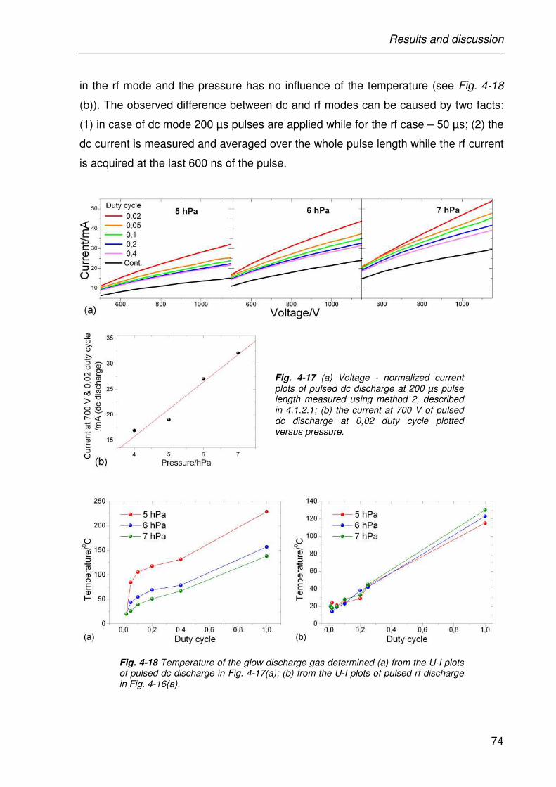
Results and discussion
74
in the rf mode and the pressure has no influence of the temperature (see Fig. 4-18
(b)). The observed difference between dc and rf modes can be caused by two facts:
(1) in case of dc mode 200 µs pulses are applied while for the rf case – 50 µs; (2) the
dc current is measured and averaged over the whole pulse length while the rf current
is acquired at the last 600 ns of the pulse.
Fig. 4-17 (a) Voltage - normalized current plots of pulsed dc discharge at 200 µs pulse length measured using method 2, described in 4.1.2.1; (b) the current at 700 V of pulsed dc discharge at 0,02 duty cycle plotted versus pressure.
Fig. 4-18 Temperature of the glow discharge gas determined (a) from the U-I plots of pulsed dc discharge in Fig. 4-17(a); (b) from the U-I plots of pulsed rf discharge in Fig. 4-16(a).
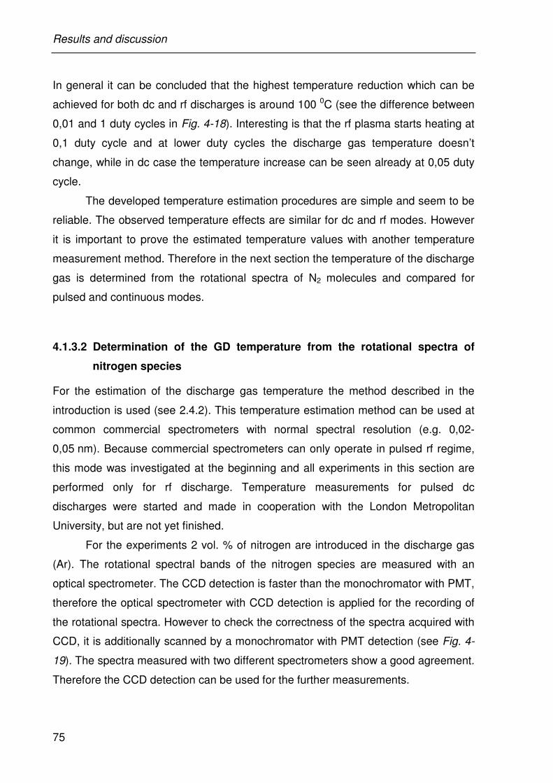
Results and discussion
75
In general it can be concluded that the highest temperature reduction which can be
achieved for both dc and rf discharges is around 100 0C (see the difference between
0,01 and 1 duty cycles in Fig. 4-18). Interesting is that the rf plasma starts heating at
0,1 duty cycle and at lower duty cycles the discharge gas temperature doesn’t
change, while in dc case the temperature increase can be seen already at 0,05 duty
cycle.
The developed temperature estimation procedures are simple and seem to be
reliable. The observed temperature effects are similar for dc and rf modes. However
it is important to prove the estimated temperature values with another temperature
measurement method. Therefore in the next section the temperature of the discharge
gas is determined from the rotational spectra of N2 molecules and compared for
pulsed and continuous modes.
4.1.3.2 Determination of the GD temperature from the rotational spectra of
nitrogen species
For the estimation of the discharge gas temperature the method described in the
introduction is used (see 2.4.2). This temperature estimation method can be used at
common commercial spectrometers with normal spectral resolution (e.g. 0,02-
0,05 nm). Because commercial spectrometers can only operate in pulsed rf regime,
this mode was investigated at the beginning and all experiments in this section are
performed only for rf discharge. Temperature measurements for pulsed dc
discharges were started and made in cooperation with the London Metropolitan
University, but are not yet finished.
For the experiments 2 vol. % of nitrogen are introduced in the discharge gas
(Ar). The rotational spectral bands of the nitrogen species are measured with an
optical spectrometer. The CCD detection is faster than the monochromator with PMT,
therefore the optical spectrometer with CCD detection is applied for the recording of
the rotational spectra. However to check the correctness of the spectra acquired with
CCD, it is additionally scanned by a monochromator with PMT detection (see Fig. 4-
19). The spectra measured with two different spectrometers show a good agreement.
Therefore the CCD detection can be used for the further measurements.
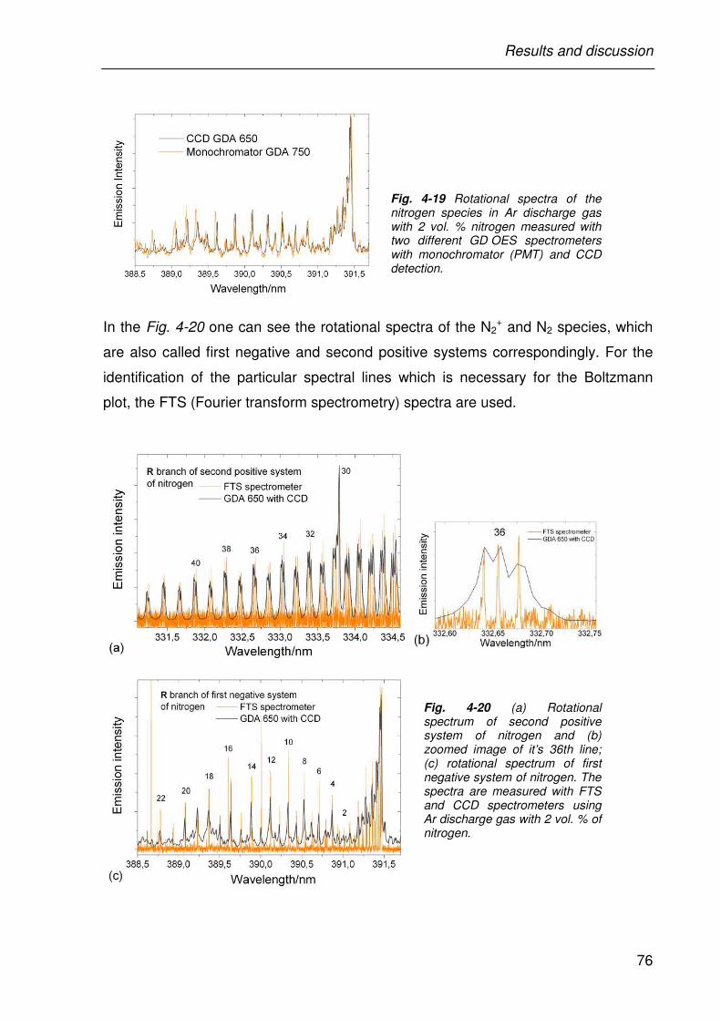
Results and discussion
76
Fig. 4-19 Rotational spectra of the nitrogen species in Ar discharge gas with 2 vol. % nitrogen measured with two different GD OES spectrometers with monochromator (PMT) and CCD detection.
In the Fig. 4-20 one can see the rotational spectra of the N2+ and N2 species, which
are also called first negative and second positive systems correspondingly. For the
identification of the particular spectral lines which is necessary for the Boltzmann
plot, the FTS (Fourier transform spectrometry) spectra are used.
Fig. 4-20 (a) Rotational spectrum of second positive system of nitrogen and (b) zoomed image of it’s 36th line; (c) rotational spectrum of first negative system of nitrogen. The spectra are measured with FTS and CCD spectrometers using Ar discharge gas with 2 vol. % of nitrogen.
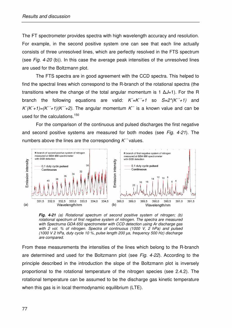
Results and discussion
77
The FT spectrometer provides spectra with high wavelength accuracy and resolution.
For example, in the second positive system one can see that each line actually
consists of three unresolved lines, which are perfectly resolved in the FTS spectrum
(see Fig. 4-20 (b)). In this case the average peak intensities of the unresolved lines
are used for the Boltzmann plot.
The FTS spectra are in good agreement with the CCD spectra. This helped to
find the spectral lines which correspond to the R-branch of the rotational spectra (the
transitions where the change of the total angular momentum is 1 ∆J=1). For the R
branch the following equations are valid: K´=K´´+1 so S=2*(K´´+1) and
K´(K´+1)=(K´´+1)(K´´+2). The angular momentum K´´ is a known value and can be
used for the calculations.150
For the comparison of the continuous and pulsed discharges the first negative
and second positive systems are measured for both modes (see Fig. 4-21). The
numbers above the lines are the corresponding K´´ values.
Fig. 4-21 (a) Rotational spectrum of second positive system of nitrogen; (b) rotational spectrum of first negative system of nitrogen. The spectra are measured with Spectruma GDA 650 spectrometer with CCD detection using Ar discharge gas with 2 vol. % of nitrogen. Spectra of continuous (1000 V, 2 hPa) and pulsed (1000 V 2 hPa, duty cycle 10 %, pulse length 200 µs, frequency 500 Hz) discharge are compared.
From these measurements the intensities of the lines which belong to the R-branch
are determined and used for the Boltzmann plot (see Fig. 4-22). According to the
principle described in the introduction the slope of the Boltzmann plot is inversely
proportional to the rotational temperature of the nitrogen species (see 2.4.2). The
rotational temperature can be assumed to be the discharge gas kinetic temperature
when this gas is in local thermodynamic equilibrium (LTE).
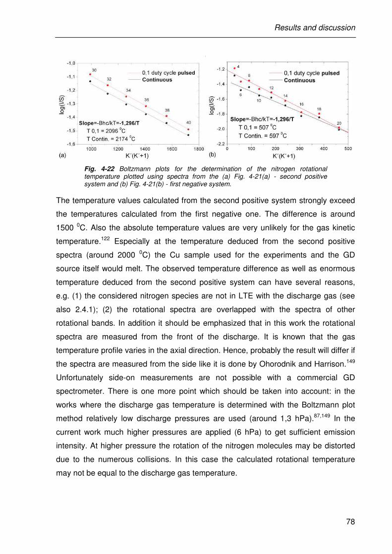
Results and discussion
78
Fig. 4-22 Boltzmann plots for the determination of the nitrogen rotational temperature plotted using spectra from the (a) Fig. 4-21(a) - second positive system and (b) Fig. 4-21(b) - first negative system.
The temperature values calculated from the second positive system strongly exceed
the temperatures calculated from the first negative one. The difference is around
1500 0C. Also the absolute temperature values are very unlikely for the gas kinetic
temperature.122 Especially at the temperature deduced from the second positive
spectra (around 2000 0C) the Cu sample used for the experiments and the GD
source itself would melt. The observed temperature difference as well as enormous
temperature deduced from the second positive system can have several reasons,
e.g. (1) the considered nitrogen species are not in LTE with the discharge gas (see
also 2.4.1); (2) the rotational spectra are overlapped with the spectra of other
rotational bands. In addition it should be emphasized that in this work the rotational
spectra are measured from the front of the discharge. It is known that the gas
temperature profile varies in the axial direction. Hence, probably the result will differ if
the spectra are measured from the side like it is done by Ohorodnik and Harrison.149
Unfortunately side-on measurements are not possible with a commercial GD
spectrometer. There is one more point which should be taken into account: in the
works where the discharge gas temperature is determined with the Boltzmann plot
method relatively low discharge pressures are used (around 1,3 hPa).87,149 In the
current work much higher pressures are applied (6 hPa) to get sufficient emission
intensity. At higher pressure the rotation of the nitrogen molecules may be distorted
due to the numerous collisions. In this case the calculated rotational temperature
may not be equal to the discharge gas temperature.
Results and discussion
79
There is one important result of the rotational temperature measurements. The
temperature difference between pulsed and continuous mode calculated from the
spectra of second positive system is 78 0C and from the spectra of first negative
system – 90 0C. These values are also close to the temperature difference deduced
from the U-I plots of the pulsed and continuous discharges - 100 0C (see 4.1.3.1).
Hence there are three different temperature estimation procedures (U-I plots,
rotational spectra of N2 and N2+) which indicate that the discharge gas temperature
can be reduced by around 100 0C when PGD is applied.
However the study of the discharge gas temperature is not completed. More
attention should be paid to the absolute value of the discharge gas temperature and
at the cathode (sample) temperature as well.
4.1.4 Study of the sputtered crater formation in the PGD
The advantages of GD sputtering (see 2.1.2) make GD OES to a suitable and fast
method for depth profiling of thin layers.48,66,205,206 Mild surface sputtering and fast
sampling time of commercial light detection systems should theoretically provide an
exceptionally high depth resolution in sub-nanometre level. Nevertheless the real
depth resolution of GD OES is limited by the ultimate depth resolution56 (some
nm38,207-209), formation of a nonplanar sputtered crater210-213 and sputter induced
roughening of the sample surface.82,214,215 Hence to reach the best possible depth
resolution (ultimate depth resolution) at GD OES depth profiling it is necessary to
optimize the analysis conditions such a way to get a most flat and smooth crater.
Besides the common discharge parameters of the GD – voltage, current and
pressure, in the case of PGD there are additional parameters – duty cycle, pulse
duration and pulse frequency (see 2.3.1). On the one hand, more discharge
parameters enable to control the heating and sputtering rate of the sample with
greater precision. But from the other hand it complicates the optimization procedure.
As a consequence, one should study the influence of all the PGD parameters on the
crater shape and roughness.
For the continuous discharge the influence of voltage, current and pressure on
the crater shape and depth resolution is well investigated.51,187-195 Also a number of
modelling works studied the crater formation and corresponding depth
Results and discussion
80
profiles.45,71,216-218 But in case of pulsed discharge very few authors consider the PGD
parameters.76-78,184,185 Oxley et al.78 suppose that pulse width and frequency have
little influence on crater shape, but Martin185 found that the pulse width plays an
important role in producing a good crater. The effect of pulsing parameters on the
sputtering rate77,184 and depth resolution76 is also studied, but only small pulse length
and frequency ranges are examined.
Apparently, PGD is a promising tool for GD OES depth profiling of thermally
sensitive and thin layered samples. Nevertheless to find optimal analysis conditions
more systematic studies on the relation between discharge parameters and crater
formation are necessary. Therefore, in the following sections the influence of all PGD
parameters (pulse duration, duty cycle as well as the electrical parameters voltage
and current) on the crater formation is studied. Pulsed dc and rf discharges are
compared in terms of sputtering rates and crater shapes. The observed changes of
the crater shape are reflected in depth profiles measured at different discharge
conditions (4.1.4.3).
4.1.4.1 Investigation of the sputtering rates
In this part the dependence of the sputtering rates on U, I, duty cycle and pulse
length is studied. These PGD parameters are sequentially considered following the
principle of varying only one parameter under investigation and keep all others
constant. In this way one can correlate the observed effect with a distinct operating
parameter.
Influence of voltage and current on sputtering rate It has been already mentioned
that voltage and current are very often considered and well studied for the continuous
discharge. As far back as 1972 Boumans62 found that the sputtering rate q linearly
depends on voltage and current (equation 2-4). The pressure is defined by the U and
I values and implicitly included in the formula. This result of experimental and
empirical work represents the dependence of the sputtering rate on voltage and
current and is especially used at quantitative GD OES analyses, where standards
with different matrix are used for calibration (see 2.2.2). Therefore it is reasonable to
check if it is valid also for pulsed discharge. For this one should consider such
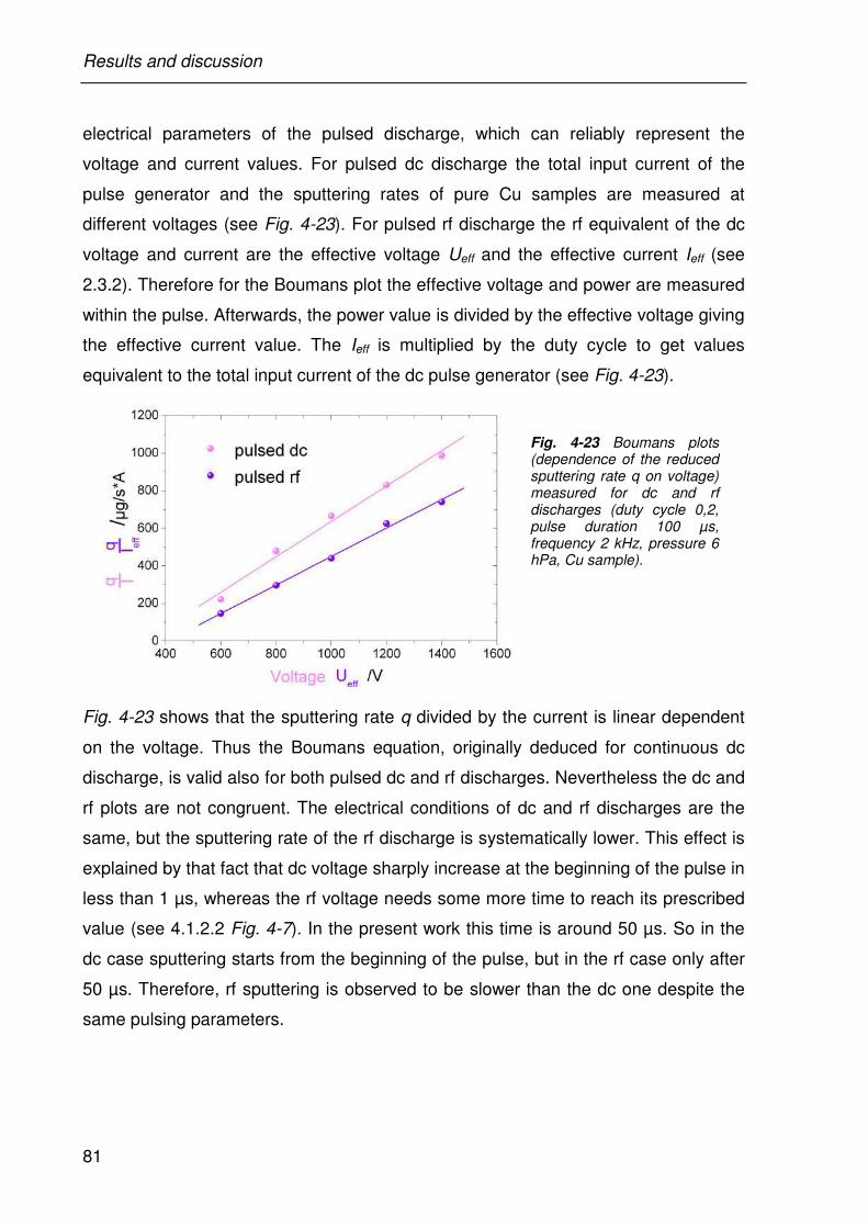
Results and discussion
81
electrical parameters of the pulsed discharge, which can reliably represent the
voltage and current values. For pulsed dc discharge the total input current of the
pulse generator and the sputtering rates of pure Cu samples are measured at
different voltages (see Fig. 4-23). For pulsed rf discharge the rf equivalent of the dc
voltage and current are the effective voltage Ueff and the effective current Ieff (see
2.3.2). Therefore for the Boumans plot the effective voltage and power are measured
within the pulse. Afterwards, the power value is divided by the effective voltage giving
the effective current value. The Ieff is multiplied by the duty cycle to get values
equivalent to the total input current of the dc pulse generator (see Fig. 4-23).
Fig. 4-23 Boumans plots (dependence of the reduced sputtering rate q on voltage) measured for dc and rf discharges (duty cycle 0,2, pulse duration 100 µs, frequency 2 kHz, pressure 6 hPa, Cu sample).
Fig. 4-23 shows that the sputtering rate q divided by the current is linear dependent
on the voltage. Thus the Boumans equation, originally deduced for continuous dc
discharge, is valid also for both pulsed dc and rf discharges. Nevertheless the dc and
rf plots are not congruent. The electrical conditions of dc and rf discharges are the
same, but the sputtering rate of the rf discharge is systematically lower. This effect is
explained by that fact that dc voltage sharply increase at the beginning of the pulse in
less than 1 µs, whereas the rf voltage needs some more time to reach its prescribed
value (see 4.1.2.2 Fig. 4-7). In the present work this time is around 50 µs. So in the
dc case sputtering starts from the beginning of the pulse, but in the rf case only after
50 µs. Therefore, rf sputtering is observed to be slower than the dc one despite the
same pulsing parameters.
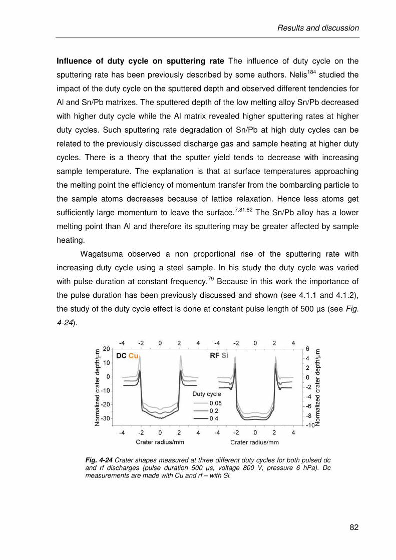
Results and discussion
82
Influence of duty cycle on sputtering rate The influence of duty cycle on the
sputtering rate has been previously described by some authors. Nelis184 studied the
impact of the duty cycle on the sputtered depth and observed different tendencies for
Al and Sn/Pb matrixes. The sputtered depth of the low melting alloy Sn/Pb decreased
with higher duty cycle while the Al matrix revealed higher sputtering rates at higher
duty cycles. Such sputtering rate degradation of Sn/Pb at high duty cycles can be
related to the previously discussed discharge gas and sample heating at higher duty
cycles. There is a theory that the sputter yield tends to decrease with increasing
sample temperature. The explanation is that at surface temperatures approaching
the melting point the efficiency of momentum transfer from the bombarding particle to
the sample atoms decreases because of lattice relaxation. Hence less atoms get
sufficiently large momentum to leave the surface.7,81,82 The Sn/Pb alloy has a lower
melting point than Al and therefore its sputtering may be greater affected by sample
heating.
Wagatsuma observed a non proportional rise of the sputtering rate with
increasing duty cycle using a steel sample. In his study the duty cycle was varied
with pulse duration at constant frequency.79 Because in this work the importance of
the pulse duration has been previously discussed and shown (see 4.1.1 and 4.1.2),
the study of the duty cycle effect is done at constant pulse length of 500 µs (see Fig.
4-24).
Fig. 4-24 Crater shapes measured at three different duty cycles for both pulsed dc and rf discharges (pulse duration 500 µs, voltage 800 V, pressure 6 hPa). Dc measurements are made with Cu and rf – with Si.
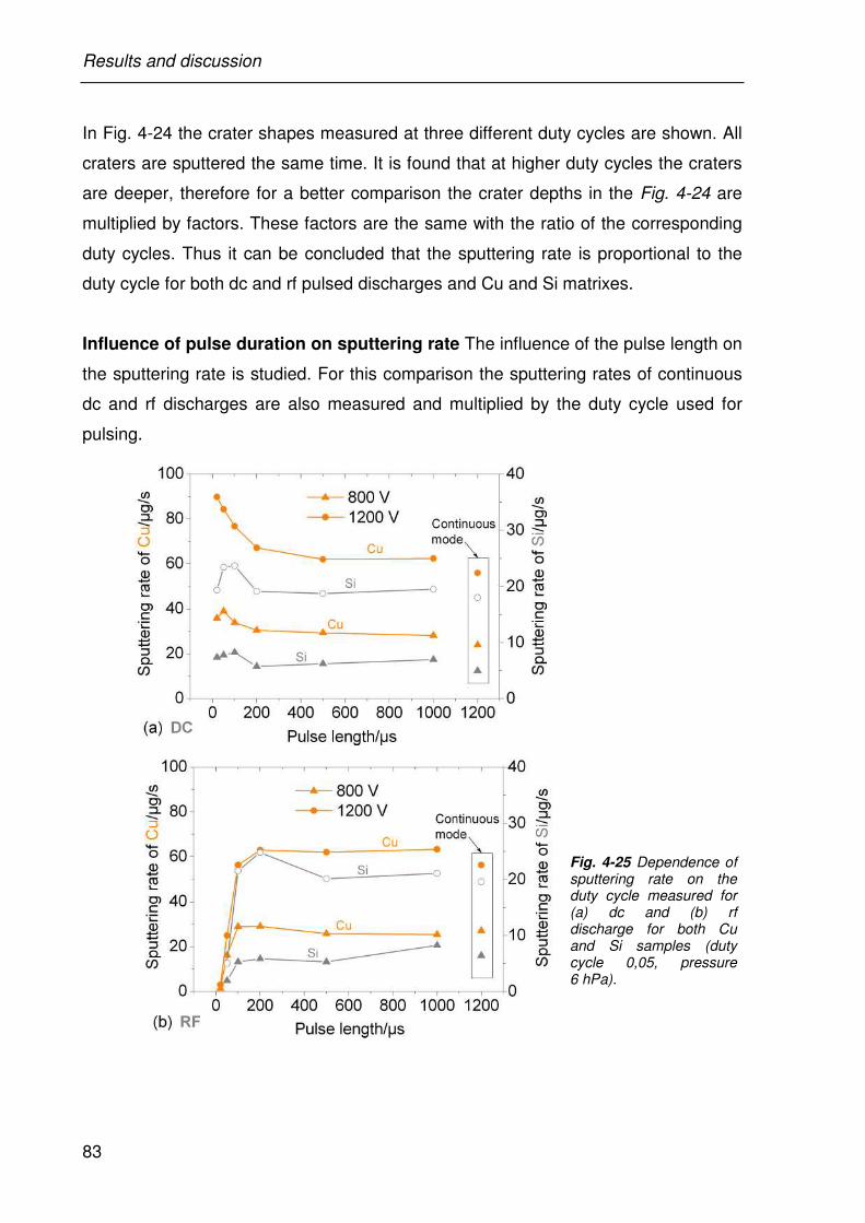
Results and discussion
83
In Fig. 4-24 the crater shapes measured at three different duty cycles are shown. All
craters are sputtered the same time. It is found that at higher duty cycles the craters
are deeper, therefore for a better comparison the crater depths in the Fig. 4-24 are
multiplied by factors. These factors are the same with the ratio of the corresponding
duty cycles. Thus it can be concluded that the sputtering rate is proportional to the
duty cycle for both dc and rf pulsed discharges and Cu and Si matrixes.
Influence of pulse duration on sputtering rate The influence of the pulse length on
the sputtering rate is studied. For this comparison the sputtering rates of continuous
dc and rf discharges are also measured and multiplied by the duty cycle used for
pulsing.
Fig. 4-25 Dependence of sputtering rate on the duty cycle measured for (a) dc and (b) rf discharge for both Cu and Si samples (duty cycle 0,05, pressure 6 hPa).
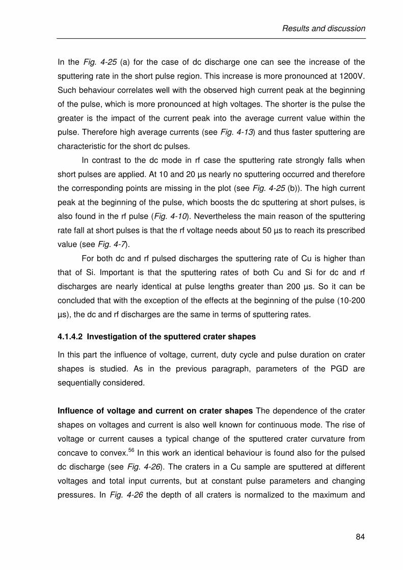
Results and discussion
84
In the Fig. 4-25 (a) for the case of dc discharge one can see the increase of the
sputtering rate in the short pulse region. This increase is more pronounced at 1200V.
Such behaviour correlates well with the observed high current peak at the beginning
of the pulse, which is more pronounced at high voltages. The shorter is the pulse the
greater is the impact of the current peak into the average current value within the
pulse. Therefore high average currents (see Fig. 4-13) and thus faster sputtering are
characteristic for the short dc pulses.
In contrast to the dc mode in rf case the sputtering rate strongly falls when
short pulses are applied. At 10 and 20 µs nearly no sputtering occurred and therefore
the corresponding points are missing in the plot (see Fig. 4-25 (b)). The high current
peak at the beginning of the pulse, which boosts the dc sputtering at short pulses, is
also found in the rf pulse (Fig. 4-10). Nevertheless the main reason of the sputtering
rate fall at short pulses is that the rf voltage needs about 50 µs to reach its prescribed
value (see Fig. 4-7).
For both dc and rf pulsed discharges the sputtering rate of Cu is higher than
that of Si. Important is that the sputtering rates of both Cu and Si for dc and rf
discharges are nearly identical at pulse lengths greater than 200 µs. So it can be
concluded that with the exception of the effects at the beginning of the pulse (10-200
µs), the dc and rf discharges are the same in terms of sputtering rates.
4.1.4.2 Investigation of the sputtered crater shapes
In this part the influence of voltage, current, duty cycle and pulse duration on crater
shapes is studied. As in the previous paragraph, parameters of the PGD are
sequentially considered.
Influence of voltage and current on crater shapes The dependence of the crater
shapes on voltages and current is also well known for continuous mode. The rise of
voltage or current causes a typical change of the sputtered crater curvature from
concave to convex.56 In this work an identical behaviour is found also for the pulsed
dc discharge (see Fig. 4-26). The craters in a Cu sample are sputtered at different
voltages and total input currents, but at constant pulse parameters and changing
pressures. In Fig. 4-26 the depth of all craters is normalized to the maximum and
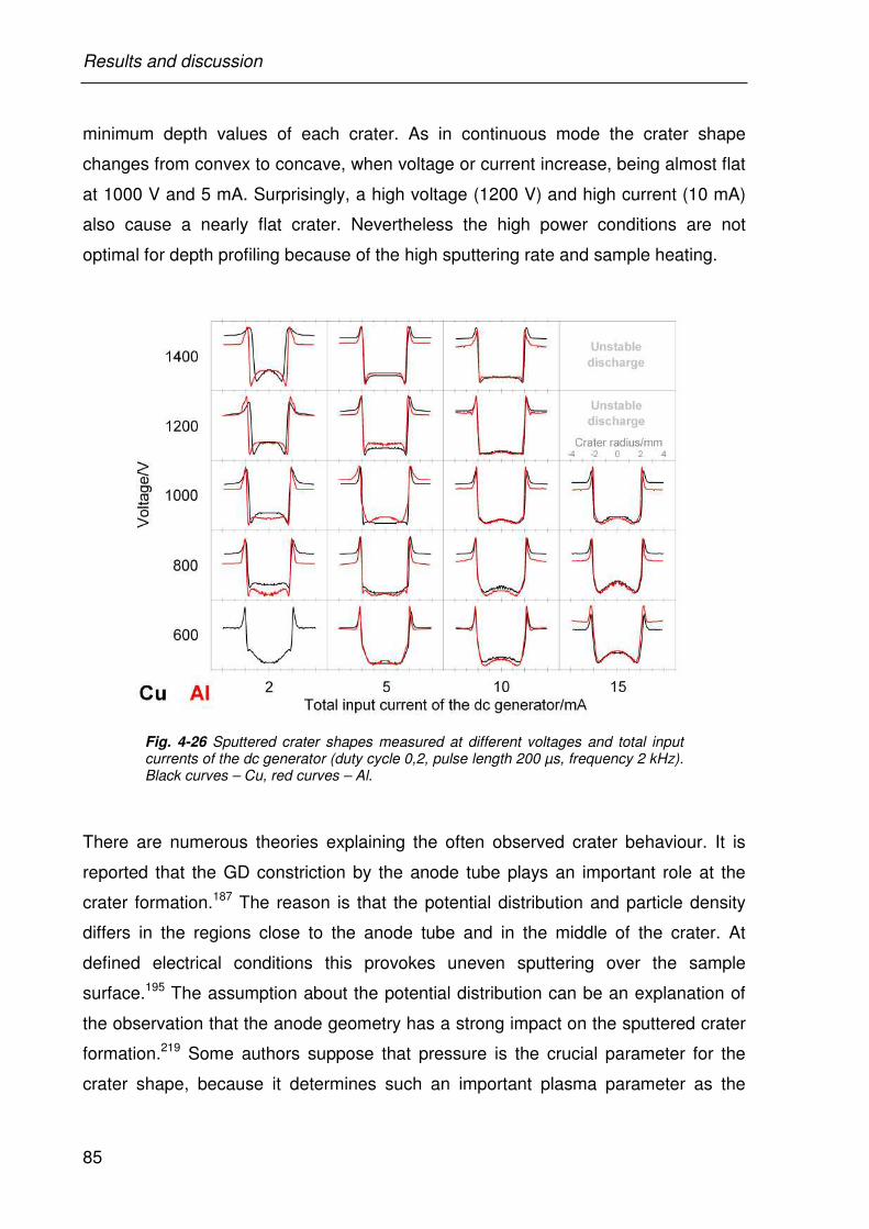
Results and discussion
85
minimum depth values of each crater. As in continuous mode the crater shape
changes from convex to concave, when voltage or current increase, being almost flat
at 1000 V and 5 mA. Surprisingly, a high voltage (1200 V) and high current (10 mA)
also cause a nearly flat crater. Nevertheless the high power conditions are not
optimal for depth profiling because of the high sputtering rate and sample heating.
Fig. 4-26 Sputtered crater shapes measured at different voltages and total input currents of the dc generator (duty cycle 0,2, pulse length 200 µs, frequency 2 kHz). Black curves – Cu, red curves – Al.
There are numerous theories explaining the often observed crater behaviour. It is
reported that the GD constriction by the anode tube plays an important role at the
crater formation.187 The reason is that the potential distribution and particle density
differs in the regions close to the anode tube and in the middle of the crater. At
defined electrical conditions this provokes uneven sputtering over the sample
surface.195 The assumption about the potential distribution can be an explanation of
the observation that the anode geometry has a strong impact on the sputtered crater
formation.219 Some authors suppose that pressure is the crucial parameter for the
crater shape, because it determines such an important plasma parameter as the
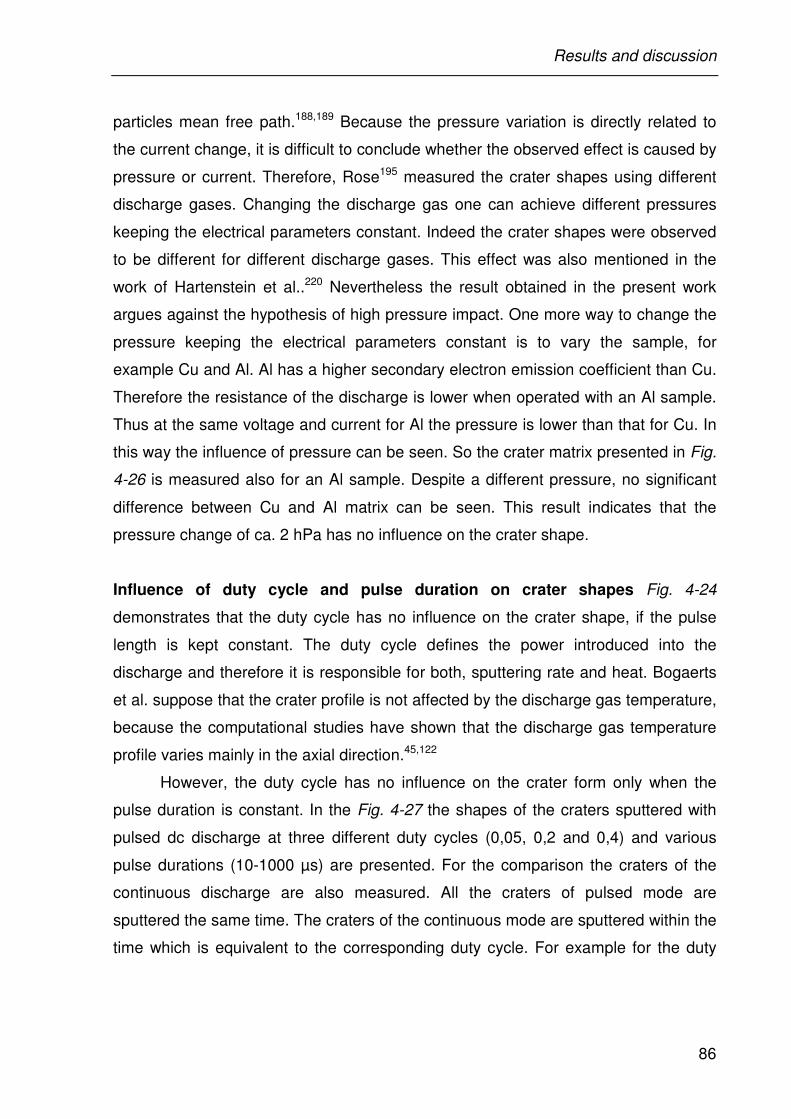
Results and discussion
86
particles mean free path.188,189 Because the pressure variation is directly related to
the current change, it is difficult to conclude whether the observed effect is caused by
pressure or current. Therefore, Rose195 measured the crater shapes using different
discharge gases. Changing the discharge gas one can achieve different pressures
keeping the electrical parameters constant. Indeed the crater shapes were observed
to be different for different discharge gases. This effect was also mentioned in the
work of Hartenstein et al..220 Nevertheless the result obtained in the present work
argues against the hypothesis of high pressure impact. One more way to change the
pressure keeping the electrical parameters constant is to vary the sample, for
example Cu and Al. Al has a higher secondary electron emission coefficient than Cu.
Therefore the resistance of the discharge is lower when operated with an Al sample.
Thus at the same voltage and current for Al the pressure is lower than that for Cu. In
this way the influence of pressure can be seen. So the crater matrix presented in Fig.
4-26 is measured also for an Al sample. Despite a different pressure, no significant
difference between Cu and Al matrix can be seen. This result indicates that the
pressure change of ca. 2 hPa has no influence on the crater shape.
Influence of duty cycle and pulse duration on crater shapes Fig. 4-24
demonstrates that the duty cycle has no influence on the crater shape, if the pulse
length is kept constant. The duty cycle defines the power introduced into the
discharge and therefore it is responsible for both, sputtering rate and heat. Bogaerts
et al. suppose that the crater profile is not affected by the discharge gas temperature,
because the computational studies have shown that the discharge gas temperature
profile varies mainly in the axial direction.45,122
However, the duty cycle has no influence on the crater form only when the
pulse duration is constant. In the Fig. 4-27 the shapes of the craters sputtered with
pulsed dc discharge at three different duty cycles (0,05, 0,2 and 0,4) and various
pulse durations (10-1000 µs) are presented. For the comparison the craters of the
continuous discharge are also measured. All the craters of pulsed mode are
sputtered the same time. The craters of the continuous mode are sputtered within the
time which is equivalent to the corresponding duty cycle. For example for the duty
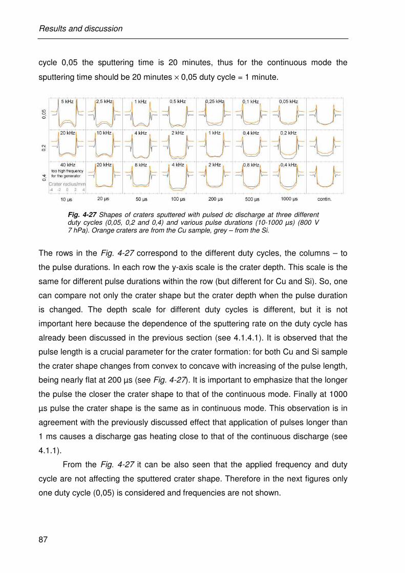
Results and discussion
87
cycle 0,05 the sputtering time is 20 minutes, thus for the continuous mode the
sputtering time should be 20 minutes × 0,05 duty cycle = 1 minute.
Fig. 4-27 Shapes of craters sputtered with pulsed dc discharge at three different duty cycles (0,05, 0,2 and 0,4) and various pulse durations (10-1000 µs) (800 V 7 hPa). Orange craters are from the Cu sample, grey – from the Si.
The rows in the Fig. 4-27 correspond to the different duty cycles, the columns – to
the pulse durations. In each row the y-axis scale is the crater depth. This scale is the
same for different pulse durations within the row (but different for Cu and Si). So, one
can compare not only the crater shape but the crater depth when the pulse duration
is changed. The depth scale for different duty cycles is different, but it is not
important here because the dependence of the sputtering rate on the duty cycle has
already been discussed in the previous section (see 4.1.4.1). It is observed that the
pulse length is a crucial parameter for the crater formation: for both Cu and Si sample
the crater shape changes from convex to concave with increasing of the pulse length,
being nearly flat at 200 µs (see Fig. 4-27). It is important to emphasize that the longer
the pulse the closer the crater shape to that of the continuous mode. Finally at 1000
µs pulse the crater shape is the same as in continuous mode. This observation is in
agreement with the previously discussed effect that application of pulses longer than
1 ms causes a discharge gas heating close to that of the continuous discharge (see
4.1.1).
From the Fig. 4-27 it can be also seen that the applied frequency and duty
cycle are not affecting the sputtered crater shape. Therefore in the next figures only
one duty cycle (0,05) is considered and frequencies are not shown.
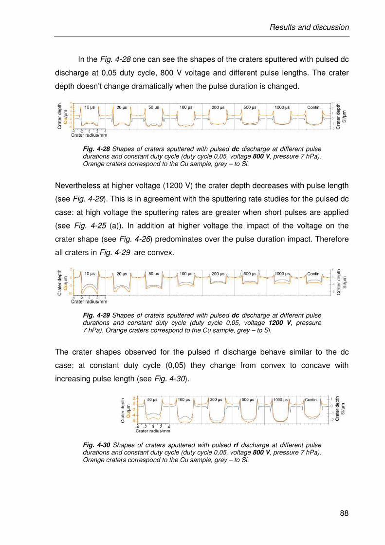
Results and discussion
88
In the Fig. 4-28 one can see the shapes of the craters sputtered with pulsed dc
discharge at 0,05 duty cycle, 800 V voltage and different pulse lengths. The crater
depth doesn’t change dramatically when the pulse duration is changed.
Fig. 4-28 Shapes of craters sputtered with pulsed dc discharge at different pulse durations and constant duty cycle (duty cycle 0,05, voltage 800 V, pressure 7 hPa). Orange craters correspond to the Cu sample, grey – to Si.
Nevertheless at higher voltage (1200 V) the crater depth decreases with pulse length
(see Fig. 4-29). This is in agreement with the sputtering rate studies for the pulsed dc
case: at high voltage the sputtering rates are greater when short pulses are applied
(see Fig. 4-25 (a)). In addition at higher voltage the impact of the voltage on the
crater shape (see Fig. 4-26) predominates over the pulse duration impact. Therefore
all craters in Fig. 4-29 are convex.
Fig. 4-29 Shapes of craters sputtered with pulsed dc discharge at different pulse durations and constant duty cycle (duty cycle 0,05, voltage 1200 V, pressure 7 hPa). Orange craters correspond to the Cu sample, grey – to Si.
The crater shapes observed for the pulsed rf discharge behave similar to the dc
case: at constant duty cycle (0,05) they change from convex to concave with
increasing pulse length (see Fig. 4-30).
Fig. 4-30 Shapes of craters sputtered with pulsed rf discharge at different pulse durations and constant duty cycle (duty cycle 0,05, voltage 800 V, pressure 7 hPa). Orange craters correspond to the Cu sample, grey – to Si.
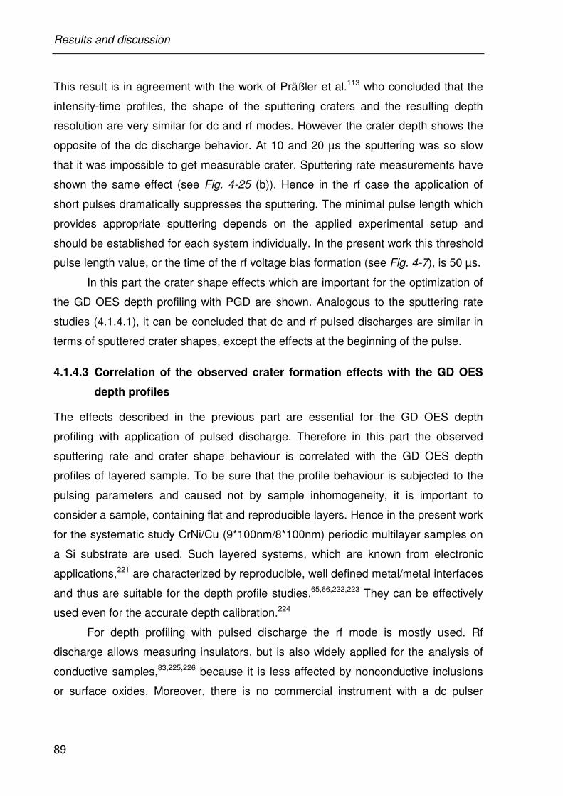
Results and discussion
89
This result is in agreement with the work of Präßler et al.113 who concluded that the
intensity-time profiles, the shape of the sputtering craters and the resulting depth
resolution are very similar for dc and rf modes. However the crater depth shows the
opposite of the dc discharge behavior. At 10 and 20 µs the sputtering was so slow
that it was impossible to get measurable crater. Sputtering rate measurements have
shown the same effect (see Fig. 4-25 (b)). Hence in the rf case the application of
short pulses dramatically suppresses the sputtering. The minimal pulse length which
provides appropriate sputtering depends on the applied experimental setup and
should be established for each system individually. In the present work this threshold
pulse length value, or the time of the rf voltage bias formation (see Fig. 4-7), is 50 µs.
In this part the crater shape effects which are important for the optimization of
the GD OES depth profiling with PGD are shown. Analogous to the sputtering rate
studies (4.1.4.1), it can be concluded that dc and rf pulsed discharges are similar in
terms of sputtered crater shapes, except the effects at the beginning of the pulse.
4.1.4.3 Correlation of the observed crater formation effects with the GD OES
depth profiles
The effects described in the previous part are essential for the GD OES depth
profiling with application of pulsed discharge. Therefore in this part the observed
sputtering rate and crater shape behaviour is correlated with the GD OES depth
profiles of layered sample. To be sure that the profile behaviour is subjected to the
pulsing parameters and caused not by sample inhomogeneity, it is important to
consider a sample, containing flat and reproducible layers. Hence in the present work
for the systematic study CrNi/Cu (9*100nm/8*100nm) periodic multilayer samples on
a Si substrate are used. Such layered systems, which are known from electronic
applications,221 are characterized by reproducible, well defined metal/metal interfaces
and thus are suitable for the depth profile studies.65,66,222,223 They can be effectively
used even for the accurate depth calibration.224
For depth profiling with pulsed discharge the rf mode is mostly used. Rf
discharge allows measuring insulators, but is also widely applied for the analysis of
conductive samples,83,225,226 because it is less affected by nonconductive inclusions
or surface oxides. Moreover, there is no commercial instrument with a dc pulser
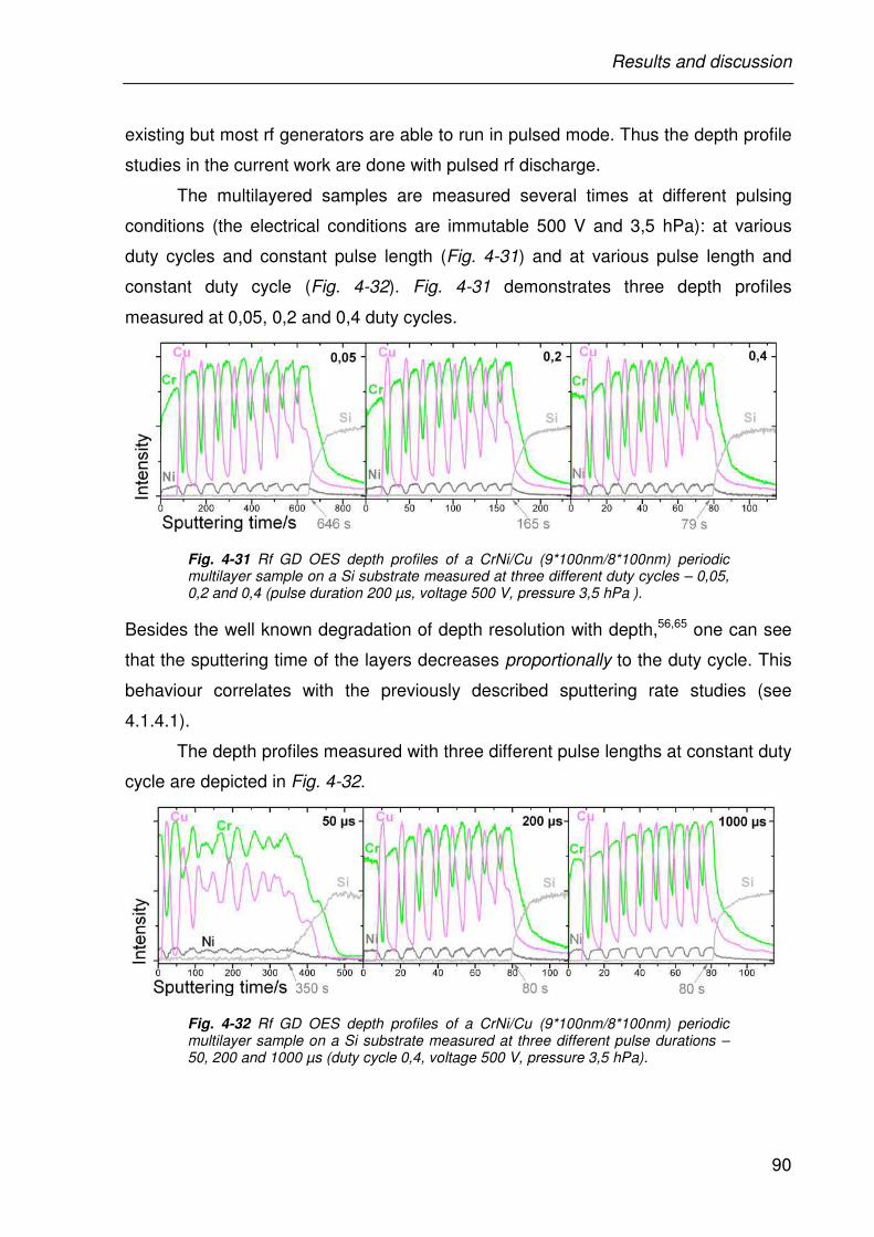
Results and discussion
90
existing but most rf generators are able to run in pulsed mode. Thus the depth profile
studies in the current work are done with pulsed rf discharge.
The multilayered samples are measured several times at different pulsing
conditions (the electrical conditions are immutable 500 V and 3,5 hPa): at various
duty cycles and constant pulse length (Fig. 4-31) and at various pulse length and
constant duty cycle (Fig. 4-32). Fig. 4-31 demonstrates three depth profiles
measured at 0,05, 0,2 and 0,4 duty cycles.
Fig. 4-31 Rf GD OES depth profiles of a CrNi/Cu (9*100nm/8*100nm) periodic multilayer sample on a Si substrate measured at three different duty cycles – 0,05, 0,2 and 0,4 (pulse duration 200 µs, voltage 500 V, pressure 3,5 hPa ).
Besides the well known degradation of depth resolution with depth,56,65 one can see
that the sputtering time of the layers decreases proportionally to the duty cycle. This
behaviour correlates with the previously described sputtering rate studies (see
4.1.4.1).
The depth profiles measured with three different pulse lengths at constant duty
cycle are depicted in Fig. 4-32.
Fig. 4-32 Rf GD OES depth profiles of a CrNi/Cu (9*100nm/8*100nm) periodic multilayer sample on a Si substrate measured at three different pulse durations – 50, 200 and 1000 µs (duty cycle 0,4, voltage 500 V, pressure 3,5 hPa).
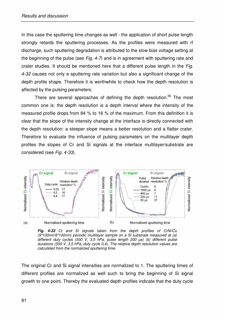
Results and discussion
91
In this case the sputtering time changes as well - the application of short pulse length
strongly retards the sputtering processes. As the profiles were measured with rf
discharge, such sputtering degradation is attributed to the slow bias voltage setting at
the beginning of the pulse (see Fig. 4-7) and is in agreement with sputtering rate and
crater studies. It should be mentioned here that a different pulse length in the Fig.
4-32 causes not only a sputtering rate variation but also a significant change of the
depth profile shape. Therefore it is worthwhile to check how the depth resolution is
affected by the pulsing parameters.
There are several approaches of defining the depth resolution.56 The most
common one is: the depth resolution is a depth interval where the intensity of the
measured profile drops from 84 % to 16 % of the maximum. From this definition it is
clear that the slope of the intensity change at the interface is directly connected with
the depth resolution: a steeper slope means a better resolution and a flatter crater.
Therefore to evaluate the influence of pulsing parameters on the multilayer depth
profiles the slopes of Cr and Si signals at the interface multilayer/substrate are
considered (see Fig. 4-33).
Fig. 4-33 Cr and Si signals taken from the depth profiles of CrNi/Cu (9*100nm/8*100nm) periodic multilayer sample on a Si substrate measured at (a) different duty cycles (500 V, 3,5 hPa, pulse length 200 µs) (b) different pulse durations (500 V, 3,5 hPa, duty cycle 0,4). The relative depth resolution values are calculated from the normalized sputtering time.
The original Cr and Si signal intensities are normalized to 1. The sputtering times of
different profiles are normalized as well such to bring the beginning of Si signal
growth to one point. Thereby the evaluated depth profiles indicate that the duty cycle
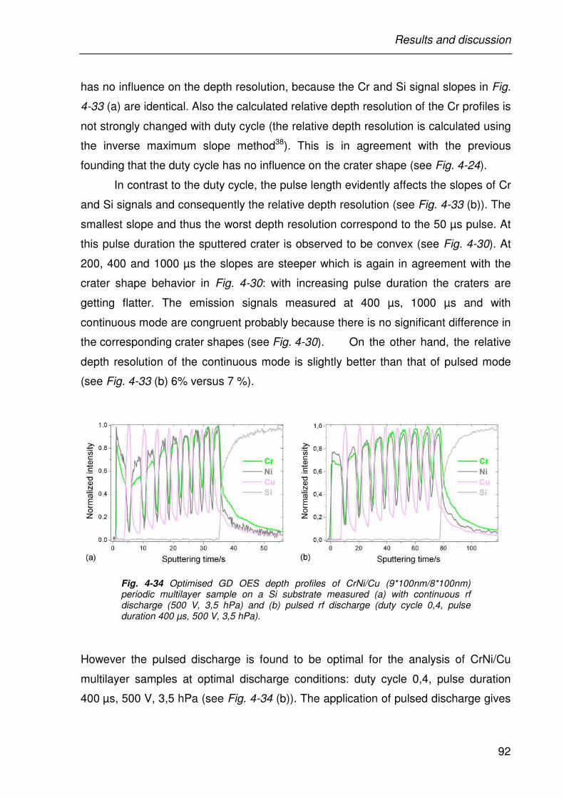
Results and discussion
92
has no influence on the depth resolution, because the Cr and Si signal slopes in Fig.
4-33 (a) are identical. Also the calculated relative depth resolution of the Cr profiles is
not strongly changed with duty cycle (the relative depth resolution is calculated using
the inverse maximum slope method38). This is in agreement with the previous
founding that the duty cycle has no influence on the crater shape (see Fig. 4-24).
In contrast to the duty cycle, the pulse length evidently affects the slopes of Cr
and Si signals and consequently the relative depth resolution (see Fig. 4-33 (b)). The
smallest slope and thus the worst depth resolution correspond to the 50 µs pulse. At
this pulse duration the sputtered crater is observed to be convex (see Fig. 4-30). At
200, 400 and 1000 µs the slopes are steeper which is again in agreement with the
crater shape behavior in Fig. 4-30: with increasing pulse duration the craters are
getting flatter. The emission signals measured at 400 µs, 1000 µs and with
continuous mode are congruent probably because there is no significant difference in
the corresponding crater shapes (see Fig. 4-30). On the other hand, the relative
depth resolution of the continuous mode is slightly better than that of pulsed mode
(see Fig. 4-33 (b) 6% versus 7 %).
Fig. 4-34 Optimised GD OES depth profiles of CrNi/Cu (9*100nm/8*100nm) periodic multilayer sample on a Si substrate measured (a) with continuous rf discharge (500 V, 3,5 hPa) and (b) pulsed rf discharge (duty cycle 0,4, pulse duration 400 µs, 500 V, 3,5 hPa).
However the pulsed discharge is found to be optimal for the analysis of CrNi/Cu
multilayer samples at optimal discharge conditions: duty cycle 0,4, pulse duration
400 µs, 500 V, 3,5 hPa (see Fig. 4-34 (b)). The application of pulsed discharge gives
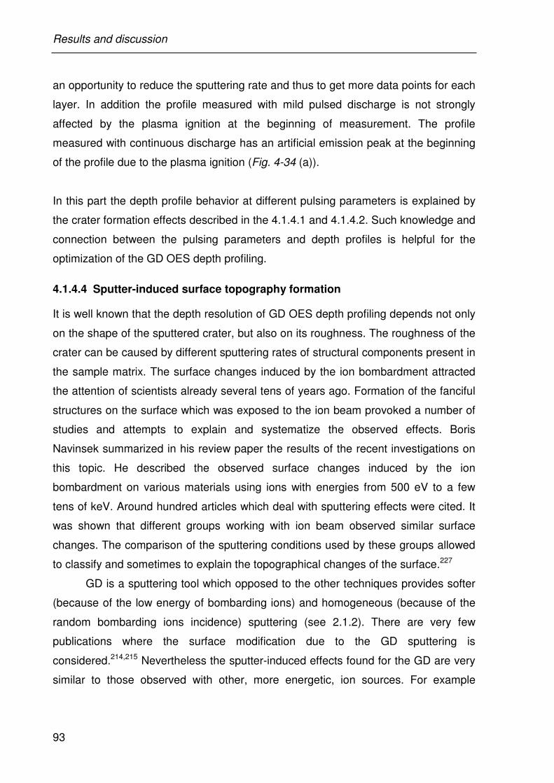
Results and discussion
93
an opportunity to reduce the sputtering rate and thus to get more data points for each
layer. In addition the profile measured with mild pulsed discharge is not strongly
affected by the plasma ignition at the beginning of measurement. The profile
measured with continuous discharge has an artificial emission peak at the beginning
of the profile due to the plasma ignition (Fig. 4-34 (a)).
In this part the depth profile behavior at different pulsing parameters is explained by
the crater formation effects described in the 4.1.4.1 and 4.1.4.2. Such knowledge and
connection between the pulsing parameters and depth profiles is helpful for the
optimization of the GD OES depth profiling.
4.1.4.4 Sputter-induced surface topography formation
It is well known that the depth resolution of GD OES depth profiling depends not only
on the shape of the sputtered crater, but also on its roughness. The roughness of the
crater can be caused by different sputtering rates of structural components present in
the sample matrix. The surface changes induced by the ion bombardment attracted
the attention of scientists already several tens of years ago. Formation of the fanciful
structures on the surface which was exposed to the ion beam provoked a number of
studies and attempts to explain and systematize the observed effects. Boris
Navinsek summarized in his review paper the results of the recent investigations on
this topic. He described the observed surface changes induced by the ion
bombardment on various materials using ions with energies from 500 eV to a few
tens of keV. Around hundred articles which deal with sputtering effects were cited. It
was shown that different groups working with ion beam observed similar surface
changes. The comparison of the sputtering conditions used by these groups allowed
to classify and sometimes to explain the topographical changes of the surface.227
GD is a sputtering tool which opposed to the other techniques provides softer
(because of the low energy of bombarding ions) and homogeneous (because of the
random bombarding ions incidence) sputtering (see 2.1.2). There are very few
publications where the surface modification due to the GD sputtering is
considered.214,215 Nevertheless the sputter-induced effects found for the GD are very
similar to those observed with other, more energetic, ion sources. For example
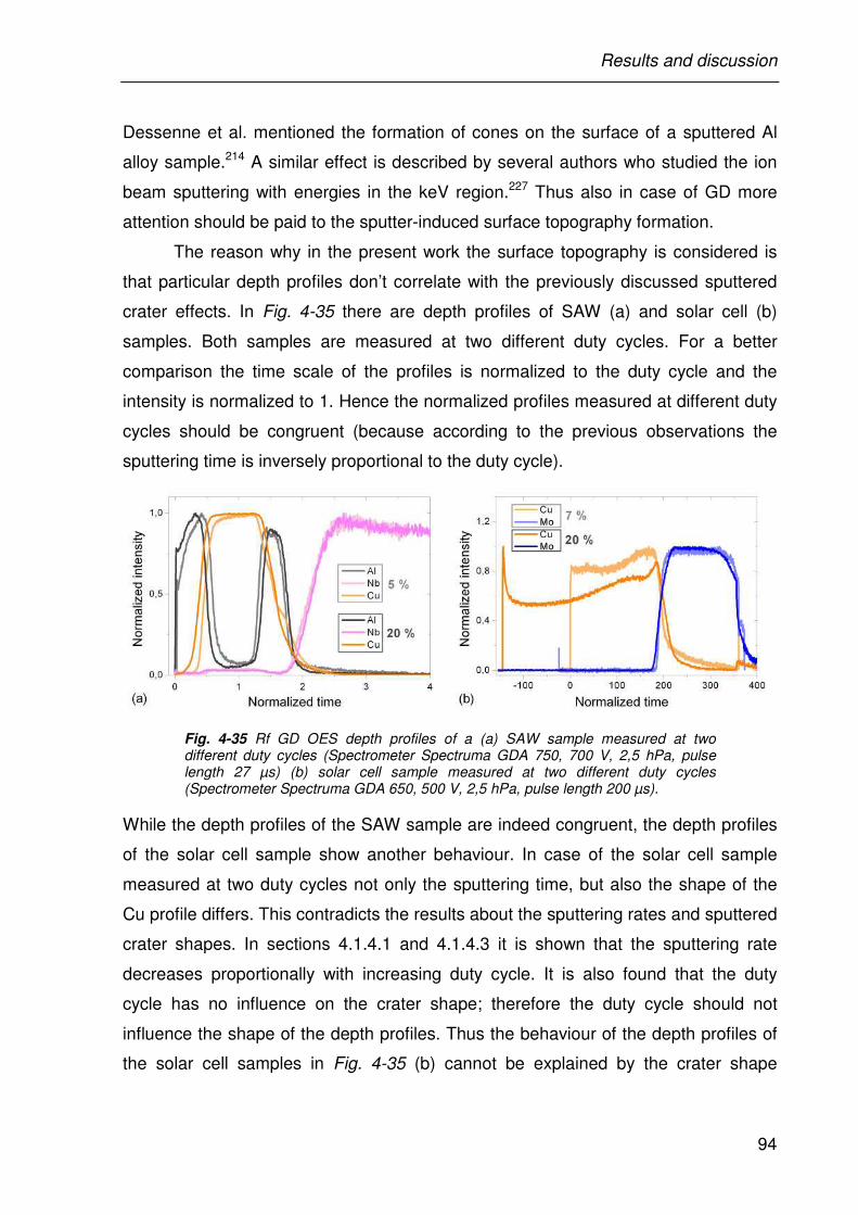
Results and discussion
94
Dessenne et al. mentioned the formation of cones on the surface of a sputtered Al
alloy sample.214 A similar effect is described by several authors who studied the ion
beam sputtering with energies in the keV region.227 Thus also in case of GD more
attention should be paid to the sputter-induced surface topography formation.
The reason why in the present work the surface topography is considered is
that particular depth profiles don’t correlate with the previously discussed sputtered
crater effects. In Fig. 4-35 there are depth profiles of SAW (a) and solar cell (b)
samples. Both samples are measured at two different duty cycles. For a better
comparison the time scale of the profiles is normalized to the duty cycle and the
intensity is normalized to 1. Hence the normalized profiles measured at different duty
cycles should be congruent (because according to the previous observations the
sputtering time is inversely proportional to the duty cycle).
Fig. 4-35 Rf GD OES depth profiles of a (a) SAW sample measured at two different duty cycles (Spectrometer Spectruma GDA 750, 700 V, 2,5 hPa, pulse length 27 µs) (b) solar cell sample measured at two different duty cycles (Spectrometer Spectruma GDA 650, 500 V, 2,5 hPa, pulse length 200 µs).
While the depth profiles of the SAW sample are indeed congruent, the depth profiles
of the solar cell sample show another behaviour. In case of the solar cell sample
measured at two duty cycles not only the sputtering time, but also the shape of the
Cu profile differs. This contradicts the results about the sputtering rates and sputtered
crater shapes. In sections 4.1.4.1 and 4.1.4.3 it is shown that the sputtering rate
decreases proportionally with increasing duty cycle. It is also found that the duty
cycle has no influence on the crater shape; therefore the duty cycle should not
influence the shape of the depth profiles. Thus the behaviour of the depth profiles of
the solar cell samples in Fig. 4-35 (b) cannot be explained by the crater shape
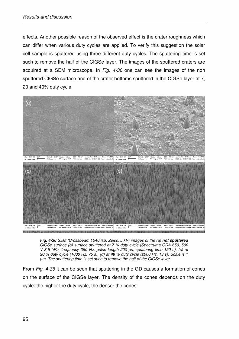
Results and discussion
95
effects. Another possible reason of the observed effect is the crater roughness which
can differ when various duty cycles are applied. To verify this suggestion the solar
cell sample is sputtered using three different duty cycles. The sputtering time is set
such to remove the half of the CIGSe layer. The images of the sputtered craters are
acquired at a SEM microscope. In Fig. 4-36 one can see the images of the non
sputtered CIGSe surface and of the crater bottoms sputtered in the CIGSe layer at 7,
20 and 40% duty cycle.
Fig. 4-36 SEM (Crossbeam 1540 XB, Zeiss, 5 kV) images of the (a) not sputtered CIGSe surface (b) surface sputtered at 7 % duty cycle (Spectruma GDA 650, 500 V 3,5 hPa, frequency 350 Hz, pulse length 200 µs, sputtering time 150 s), (c) at 20 % duty cycle (1000 Hz, 75 s), (d) at 40 % duty cycle (2000 Hz, 13 s). Scale is 1 µm. The sputtering time is set such to remove the half of the CIGSe layer.
From Fig. 4-36 it can be seen that sputtering in the GD causes a formation of cones
on the surface of the CIGSe layer. The density of the cones depends on the duty
cycle: the higher the duty cycle, the denser the cones.
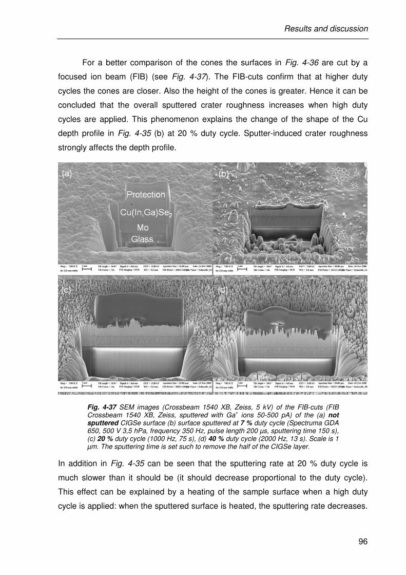
Results and discussion
96
For a better comparison of the cones the surfaces in Fig. 4-36 are cut by a
focused ion beam (FIB) (see Fig. 4-37). The FIB-cuts confirm that at higher duty
cycles the cones are closer. Also the height of the cones is greater. Hence it can be
concluded that the overall sputtered crater roughness increases when high duty
cycles are applied. This phenomenon explains the change of the shape of the Cu
depth profile in Fig. 4-35 (b) at 20 % duty cycle. Sputter-induced crater roughness
strongly affects the depth profile.
Fig. 4-37 SEM images (Crossbeam 1540 XB, Zeiss, 5 kV) of the FIB-cuts (FIB Crossbeam 1540 XB, Zeiss, sputtered with Ga
+ ions 50-500 pA) of the (a) not
sputtered CIGSe surface (b) surface sputtered at 7 % duty cycle (Spectruma GDA 650, 500 V 3,5 hPa, frequency 350 Hz, pulse length 200 µs, sputtering time 150 s), (c) 20 % duty cycle (1000 Hz, 75 s), (d) 40 % duty cycle (2000 Hz, 13 s). Scale is 1 µm. The sputtering time is set such to remove the half of the CIGSe layer.
In addition in Fig. 4-35 can be seen that the sputtering rate at 20 % duty cycle is
much slower than it should be (it should decrease proportional to the duty cycle).
This effect can be explained by a heating of the sample surface when a high duty
cycle is applied: when the sputtered surface is heated, the sputtering rate decreases.
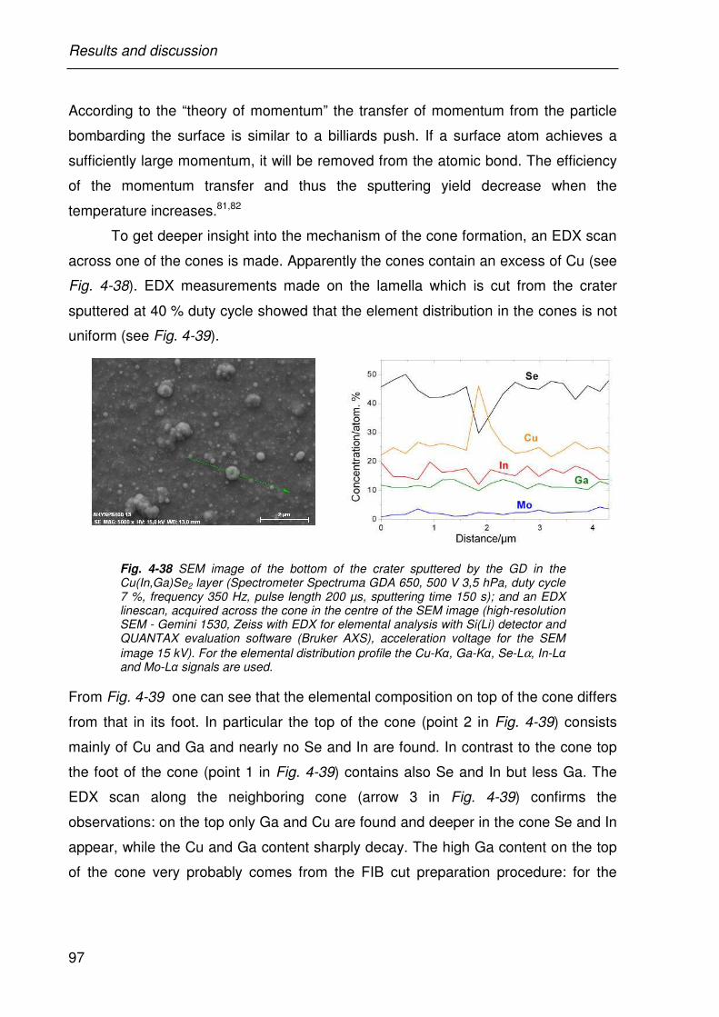
Results and discussion
97
According to the “theory of momentum” the transfer of momentum from the particle
bombarding the surface is similar to a billiards push. If a surface atom achieves a
sufficiently large momentum, it will be removed from the atomic bond. The efficiency
of the momentum transfer and thus the sputtering yield decrease when the
temperature increases.81,82
To get deeper insight into the mechanism of the cone formation, an EDX scan
across one of the cones is made. Apparently the cones contain an excess of Cu (see
Fig. 4-38). EDX measurements made on the lamella which is cut from the crater
sputtered at 40 % duty cycle showed that the element distribution in the cones is not
uniform (see Fig. 4-39).
Fig. 4-38 SEM image of the bottom of the crater sputtered by the GD in the Cu(In,Ga)Se2 layer (Spectrometer Spectruma GDA 650, 500 V 3,5 hPa, duty cycle 7 %, frequency 350 Hz, pulse length 200 µs, sputtering time 150 s); and an EDX linescan, acquired across the cone in the centre of the SEM image (high-resolution SEM - Gemini 1530, Zeiss with EDX for elemental analysis with Si(Li) detector and QUANTAX evaluation software (Bruker AXS), acceleration voltage for the SEM
image 15 kV). For the elemental distribution profile the Cu-Kα, Ga-Kα, Se-Lα, In-Lα and Mo-Lα signals are used.
From Fig. 4-39 one can see that the elemental composition on top of the cone differs
from that in its foot. In particular the top of the cone (point 2 in Fig. 4-39) consists
mainly of Cu and Ga and nearly no Se and In are found. In contrast to the cone top
the foot of the cone (point 1 in Fig. 4-39) contains also Se and In but less Ga. The
EDX scan along the neighboring cone (arrow 3 in Fig. 4-39) confirms the
observations: on the top only Ga and Cu are found and deeper in the cone Se and In
appear, while the Cu and Ga content sharply decay. The high Ga content on the top
of the cone very probably comes from the FIB cut preparation procedure: for the
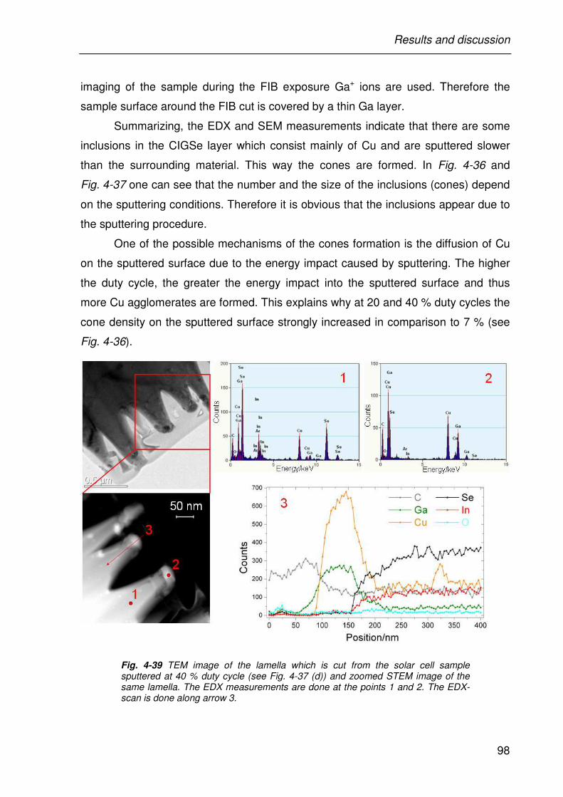
Results and discussion
98
imaging of the sample during the FIB exposure Ga+ ions are used. Therefore the
sample surface around the FIB cut is covered by a thin Ga layer.
Summarizing, the EDX and SEM measurements indicate that there are some
inclusions in the CIGSe layer which consist mainly of Cu and are sputtered slower
than the surrounding material. This way the cones are formed. In Fig. 4-36 and
Fig. 4-37 one can see that the number and the size of the inclusions (cones) depend
on the sputtering conditions. Therefore it is obvious that the inclusions appear due to
the sputtering procedure.
One of the possible mechanisms of the cones formation is the diffusion of Cu
on the sputtered surface due to the energy impact caused by sputtering. The higher
the duty cycle, the greater the energy impact into the sputtered surface and thus
more Cu agglomerates are formed. This explains why at 20 and 40 % duty cycles the
cone density on the sputtered surface strongly increased in comparison to 7 % (see
Fig. 4-36).
Fig. 4-39 TEM image of the lamella which is cut from the solar cell sample sputtered at 40 % duty cycle (see Fig. 4-37 (d)) and zoomed STEM image of the same lamella. The EDX measurements are done at the points 1 and 2. The EDX-scan is done along arrow 3.
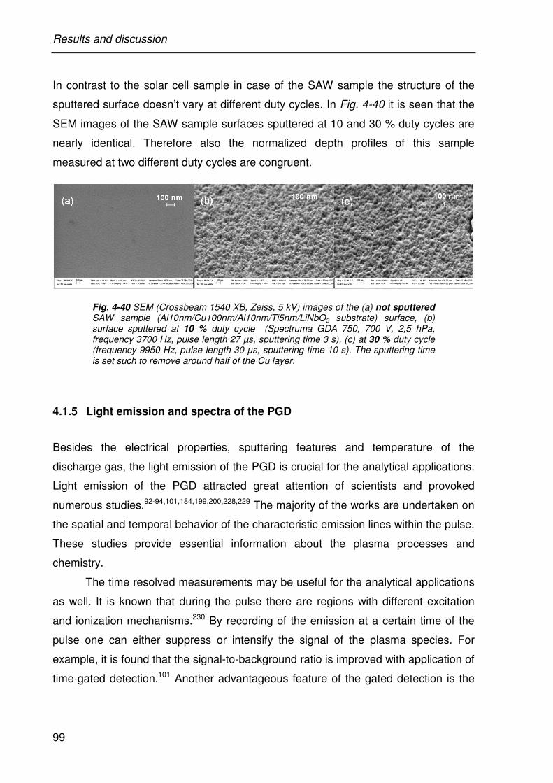
Results and discussion
99
In contrast to the solar cell sample in case of the SAW sample the structure of the
sputtered surface doesn’t vary at different duty cycles. In Fig. 4-40 it is seen that the
SEM images of the SAW sample surfaces sputtered at 10 and 30 % duty cycles are
nearly identical. Therefore also the normalized depth profiles of this sample
measured at two different duty cycles are congruent.
Fig. 4-40 SEM (Crossbeam 1540 XB, Zeiss, 5 kV) images of the (a) not sputtered SAW sample (Al10nm/Cu100nm/Al10nm/Ti5nm/LiNbO3 substrate) surface, (b) surface sputtered at 10 % duty cycle (Spectruma GDA 750, 700 V, 2,5 hPa, frequency 3700 Hz, pulse length 27 µs, sputtering time 3 s), (c) at 30 % duty cycle (frequency 9950 Hz, pulse length 30 µs, sputtering time 10 s). The sputtering time is set such to remove around half of the Cu layer.
4.1.5 Light emission and spectra of the PGD
Besides the electrical properties, sputtering features and temperature of the
discharge gas, the light emission of the PGD is crucial for the analytical applications.
Light emission of the PGD attracted great attention of scientists and provoked
numerous studies.92-94,101,184,199,200,228,229 The majority of the works are undertaken on
the spatial and temporal behavior of the characteristic emission lines within the pulse.
These studies provide essential information about the plasma processes and
chemistry.
The time resolved measurements may be useful for the analytical applications
as well. It is known that during the pulse there are regions with different excitation
and ionization mechanisms.230 By recording of the emission at a certain time of the
pulse one can either suppress or intensify the signal of the plasma species. For
example, it is found that the signal-to-background ratio is improved with application of
time-gated detection.101 Another advantageous feature of the gated detection is the
Results and discussion
100
reduced curvature of the calibration curves when the emission signal only at the
beginning of the pulse is acquired and used as analytical signal.84,184,229 This
phenomenon is explained by the reduced reabsorbtion of the emitted light during the
first microseconds of the discharge when the sputtered material is not yet completely
diffused.101 Hence the time-gated detection in GD OES devices is proved to be
useful. However it adds complexity, and cost to the instrumentation and thereby is
not implemented at the commercial scale till nowadays.
In the works which deal with gated emission only some defined, mostly atomic
emission lines are considered.92-94,228,229 There is no systematic investigation of the
correlation between the pulsing parameters and the spectrum of the PGD. Therefore
in the present work the influence of the duty cycle and pulse duration on the spectra
of both dc and rf pulsed discharges is studied by means of a commercial GD OES
spectrometer with CCD detection.
At this point two types of light detection should be briefly compared – PMT
(Photomultiplier tube) and CCD (Charge-coupled Device). The spectrometers applied
in the present studies measure the emission signal with PMT detectors every 500 µs
or acquire the overall emission every 10 ms (min.) with CCD arrays. On the one hand
the PMT detection is faster and necessary for the analysis of thin layers (10 nm and
less as in SAW samples). But on the other hand PMTs measure at some moments
irrespective to that if they are within the pulse or between the pulses. Therefore PMT
signals may contain measurement artifacts like in Fig. 4-41. In contrast to the PMT,
the CCD signal in Fig. 4-41 is immutable, because the CCD detector averages the
emission signal over the pulses. Furthermore CCDs are able to record the
continuous spectrum simultaneously. In Fig. 4-41 the depth profile of a solar cell
sample (Cu(In,Ga)Se2/Mo) measured in the 100-700 nm spectral range is shown. So
in the present studies the CCD detection is used for the investigation of the emission
spectra and the PMT is applied for fast time resolved measurements.
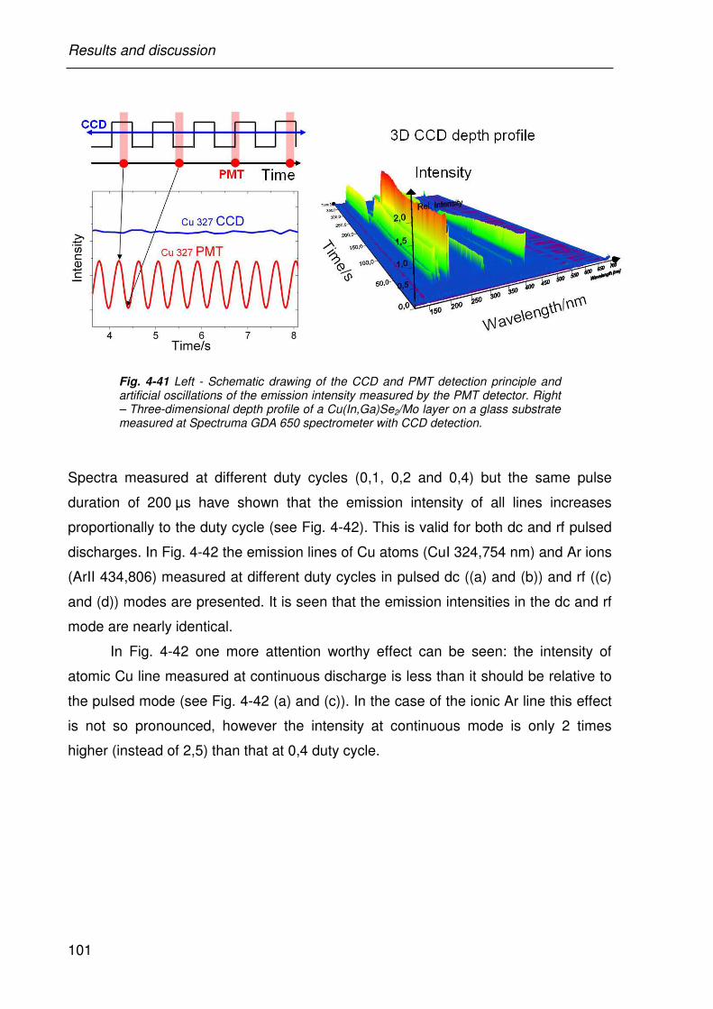
Results and discussion
101
Fig. 4-41 Left - Schematic drawing of the CCD and PMT detection principle and artificial oscillations of the emission intensity measured by the PMT detector. Right – Three-dimensional depth profile of a Cu(In,Ga)Se2/Mo layer on a glass substrate measured at Spectruma GDA 650 spectrometer with CCD detection.
Spectra measured at different duty cycles (0,1, 0,2 and 0,4) but the same pulse
duration of 200 µs have shown that the emission intensity of all lines increases
proportionally to the duty cycle (see Fig. 4-42). This is valid for both dc and rf pulsed
discharges. In Fig. 4-42 the emission lines of Cu atoms (CuI 324,754 nm) and Ar ions
(ArII 434,806) measured at different duty cycles in pulsed dc ((a) and (b)) and rf ((c)
and (d)) modes are presented. It is seen that the emission intensities in the dc and rf
mode are nearly identical.
In Fig. 4-42 one more attention worthy effect can be seen: the intensity of
atomic Cu line measured at continuous discharge is less than it should be relative to
the pulsed mode (see Fig. 4-42 (a) and (c)). In the case of the ionic Ar line this effect
is not so pronounced, however the intensity at continuous mode is only 2 times
higher (instead of 2,5) than that at 0,4 duty cycle.
Results and discussion
102
Fig. 4-42 Characteristic emission lines of (a),(c) atomic Cu and (b),(d) ionic Ar measured at different duty cycles but the same pulse length of 200 µs for both pulsed dc (a),(b) and rf (c),(d) mode.
To examine the influence of the pulse length on the light emission of PGD emission
spectra are measured at different pulse durations (20-1000 µs) but at constant duty
cycle of 0,2. These measurements have shown that even at constant duty cycle,
which is responsible for the power introduced into the discharge source, the pulse
duration significantly affects the emission intensity. Furthermore this influence differs
for various emission lines. Detailed examination of the spectra revealed that in case
of pulsed dc discharge the intensity of atomic lines rises with decrease of the pulse
length (see Fig. 4-43). The important feature is that at a pulse length of 20 µs the
emission intensity of the pulsed dc discharge reaches the same intensity level as the
continuous discharge (see Fig. 4-43 (a) and (c)). In contrast to the atomic emission
lines, the intensity of ionic lines of pulsed dc discharge is weaker than that of
continuous mode and approximately proportional to the duty cycle (see Fig. 4-43 (b)
Results and discussion
103
and (d)). The pulse length doesn’t have significant influence on the emission intensity
of the ionic emission lines (see Fig. 4-43) (b) and (d)).
Fig. 4-43 Characteristic emission lines of (a) atomic Cu, (b) ionic Cu, (c) atomic Ar, (d) ionic Ar measured at different pulse durations but the same duty cycle of 0,2 with pulsed dc discharge.
The phenomena observed for the pulsed dc mode are found also in case of the
pulsed rf mode (see Fig. 4-44). The line intensities of pulsed rf and dc discharges are
similar as well. The only difference between dc and rf discharges is that in case of
the rf mode the emission intensity is strongly suppressed when short pulses (20 or
50 µs) are applied (see Fig. 4-44). This effect is partly explained by the previously
discussed bias formation procedure at the beginning of the pulse (see part 4.1.2.2).
The rf voltage needs around 50 µs after the pulse ignition to reach its prescribed
value. Therefore the light emission as well as the sputtering rate is found to be
reduced when pulses shorter than 50 µs are applied.
Results and discussion
104
Fig. 4-44 Characteristic emission lines of (a) atomic Cu, (b) ionic Cu, (c) atomic Ar, (d) ionic Ar measured at different pulse durations but the same duty cycle of 0,2 with pulsed rf discharge.
To understand the different behavior of the atomic and ionic spectral lines fast time
resolved measurements of the emission within the pulse are undertaken using a PMT
detector. For this experiment two atomic (CuI 324,754 nm and ArI 415,859 nm) and
two ionic (CuII 224,700 nm and ArII 434,806 nm) spectral lines are selected (Fig.
4-45). It is found that for both pulsed dc and rf modes the atomic lines show a strong
enhanced emission intensity in the first 50 µs of the pulse (see Fig. 4-45 (a) and (b)),
whereas the ionic lines have only a small emission peak at the beginning of the pulse
(see Fig. 4-45 (c) and (d)), which is most probably caused by the accoustic waves
generation.204 The intensified emission of atomic lines when short pulses are applied
is already mentioned in the literature.184,229 On the other hand in case of rf discharge
the observed emission peak of the atomic lines at the beginning of the pulse (see
Fig. 4-45 (a) and (b)) is in contradiction with Fig. 4-44 (a) and (c) where those line
intensities are strongly reduced when short pulses are applied.
Results and discussion
105
It must be mentioned that time resolved intensity measurements were done only for
1000 µs long pulses and 0,2 duty cycle. Therefore changes of the intensity as
function of time are possible and must be expected, if other pulse lengths and duty
cycles are used. Furthermore, for the measurements the upper limit of the current
amplifier bandwidth (1 MHz @ 1 mA/V, see 3.3) is applied. This means that there
may be e.g. a light emission in the first µs, which cannot be resolved with the used
equipment. Last but not least there are small differences between the instrumentation
used for the time resolved PMT and the CCD measurements (e.g. another but very
similar rf generator).
Fig. 4-45 Time resolved measurements of the characteristic emission line of (a) atomic Cu (b) atomic Ar (c) ionic Cu (d) ionic Ar measured within the 1 ms pulse for both pulsed dc and rf discharges.
It can be concluded that in case of pulsed dc discharge the emission intensity of ions
is not much influenced by the pulse duration. In contrast, the emission intensity of the
atomic lines is higher at short pulses due to the observed emission prepeak. This
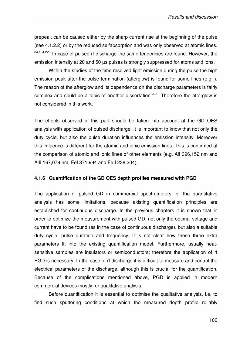
Results and discussion
106
prepeak can be caused either by the sharp current rise at the beginning of the pulse
(see 4.1.2.2) or by the reduced selfabsorption and was only observed at atomic lines. 84,184,229 In case of pulsed rf discharge the same tendencies are found. However, the
emission intensity at 20 and 50 µs pulses is strongly suppressed for atoms and ions.
Within the studies of the time resolved light emission during the pulse the high
emission peak after the pulse termination (afterglow) is found for some lines (e.g. ).
The reason of the afterglow and its dependence on the discharge parameters is fairly
complex and could be a topic of another dissertation.228 Therefore the afterglow is
not considered in this work.
The effects observed in this part should be taken into account at the GD OES
analysis with application of pulsed discharge. It is important to know that not only the
duty cycle, but also the pulse duration influences the emission intensity. Moreover
this influence is different for the atomic and ionic emission lines. This is confirmed at
the comparison of atomic and ionic lines of other elements (e.g. AlI 396,152 nm and
AlII 167,079 nm, FeI 371,994 and FeII 238,204).
4.1.6 Quantification of the GD OES depth profiles measured with PGD
The application of pulsed GD in commercial spectrometers for the quantitative
analysis has some limitations, because existing quantification principles are
established for continuous discharge. In the previous chapters it is shown that in
order to optimize the measurement with pulsed GD, not only the optimal voltage and
current have to be found (as in the case of continuous discharge), but also a suitable
duty cycle, pulse duration and frequency. It is not clear how these three extra
parameters fit into the existing quantification model. Furthermore, usually heat-
sensitive samples are insulators or semiconductors; therefore the application of rf
PGD is necessary. In the case of rf discharge it is difficult to measure and control the
electrical parameters of the discharge, although this is crucial for the quantification.
Because of the complications mentioned above, PGD is applied in modern
commercial devices mostly for qualitative analysis.
Before quantification it is essential to optimise the qualitative analysis, i.e. to
find such sputtering conditions at which the measured depth profile reliably
Results and discussion
107
represents the real element distribution in the sample. The solar cell samples are
thermally sensitive due to the glass substrate; the SAW samples contain very thin
layers in nm range. Therefore the main criteria which are important for a successful
depth profiling of these samples are: flat sputtered crater, minimal thermal stress and
moderate sputtering rates. Taking into account these criteria and the observed
influence of the PGD parameters on the crater shapes, sputtering rates, plasma
heating and surface topography, the optimal analysis conditions are found. In Fig.
4-46 one can see the optimised GD OES depth profiles of solar cell and SAW
samples.
Fig. 4-46 Rf GD OES depth profile of the (a) solar cell sample (Spectruma GDA 650, CCD detection, 500 V, 3,5 hPa, pulse length 200 µs, frequency 350 Hz, duty cycle 0,07) and (b) SAW sample (Spectruma GDA 750, PMT detection, 700 V, 2,5 hPa, pulse length 200 µs, frequency 500 Hz, duty cycle 0,1).
In the following sections the quantitative GD OES analysis of the solar cell and SAW
samples measured with pulsed GD is presented. The validity of both quantification
algorithms, described in the introduction, is checked for pulsed rf discharge.
As the pulsing parameters (duty cycle, pulse length and frequency) are found
to have a strong influence on the crater shapes, sputtering rates, plasma heating and
surface topography, for quantification they are not changed.
Regarding the electrical parameters of the PGD - the significance of the GD
voltage and current for the quantitative GD OES analysis is already mentioned in the
introduction. It is important to keep these parameters constant while measuring
standard and unknown samples, because according to the Boumans law the
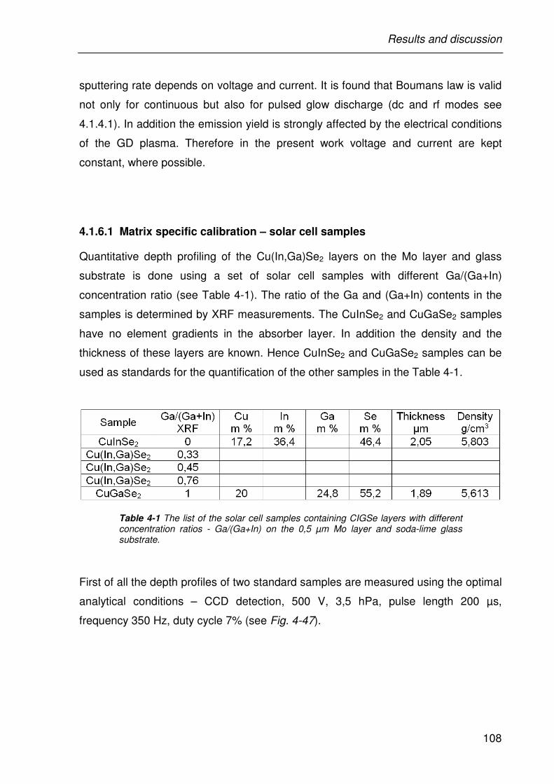
Results and discussion
108
sputtering rate depends on voltage and current. It is found that Boumans law is valid
not only for continuous but also for pulsed glow discharge (dc and rf modes see
4.1.4.1). In addition the emission yield is strongly affected by the electrical conditions
of the GD plasma. Therefore in the present work voltage and current are kept
constant, where possible.
4.1.6.1 Matrix specific calibration – solar cell samples
Quantitative depth profiling of the Cu(In,Ga)Se2 layers on the Mo layer and glass
substrate is done using a set of solar cell samples with different Ga/(Ga+In)
concentration ratio (see Table 4-1). The ratio of the Ga and (Ga+In) contents in the
samples is determined by XRF measurements. The CuInSe2 and CuGaSe2 samples
have no element gradients in the absorber layer. In addition the density and the
thickness of these layers are known. Hence CuInSe2 and CuGaSe2 samples can be
used as standards for the quantification of the other samples in the Table 4-1.
Table 4-1 The list of the solar cell samples containing CIGSe layers with different concentration ratios - Ga/(Ga+In) on the 0,5 µm Mo layer and soda-lime glass substrate.
First of all the depth profiles of two standard samples are measured using the optimal
analytical conditions – CCD detection, 500 V, 3,5 hPa, pulse length 200 µs,
frequency 350 Hz, duty cycle 7% (see Fig. 4-47).
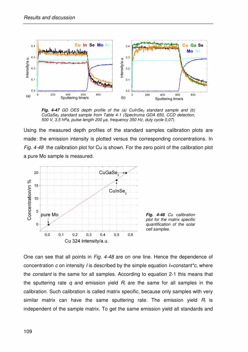
Results and discussion
109
Fig. 4-47 GD OES depth profile of the (a) CuInSe2 standard sample and (b) CuGaSe2 standard sample from Table 4-1 (Spectruma GDA 650, CCD detection, 500 V, 3,5 hPa, pulse length 200 µs, frequency 350 Hz, duty cycle 0,07).
Using the measured depth profiles of the standard samples calibration plots are
made: the emission intensity is plotted versus the corresponding concentrations. In
Fig. 4-48 the calibration plot for Cu is shown. For the zero point of the calibration plot
a pure Mo sample is measured.
Fig. 4-48 Cu calibration plot for the matrix specific quantification of the solar cell samples.
One can see that all points in Fig. 4-48 are on one line. Hence the dependence of
concentration c on intensity I is described by the simple equation I=constant*c, where
the constant is the same for all samples. According to equation 2-1 this means that
the sputtering rate q and emission yield Ri are the same for all samples in the
calibration. Such calibration is called matrix specific, because only samples with very
similar matrix can have the same sputtering rate. The emission yield Ri is
independent of the sample matrix. To get the same emission yield all standards and
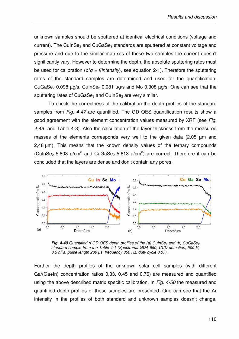
Results and discussion
110
unknown samples should be sputtered at identical electrical conditions (voltage and
current). The CuInSe2 and CuGaSe2 standards are sputtered at constant voltage and
pressure and due to the similar matrixes of these two samples the current doesn’t
significantly vary. However to determine the depth, the absolute sputtering rates must
be used for calibration (c*q = f(intensity), see equation 2-1). Therefore the sputtering
rates of the standard samples are determined and used for the quantification:
CuGaSe2 0,098 µg/s, CuInSe2 0,081 µg/s and Mo 0,308 µg/s. One can see that the
sputtering rates of CuGaSe2 and CuInSe2 are very similar.
To check the correctness of the calibration the depth profiles of the standard
samples from Fig. 4-47 are quantified. The GD OES quantification results show a
good agreement with the element concentration values measured by XRF (see Fig.
4-49 and Table 4-3). Also the calculation of the layer thickness from the measured
masses of the elements corresponds very well to the given data (2,05 µm and
2,48 µm). This means that the known density values of the ternary compounds
(CuInSe2 5.803 g/cm3 and CuGaSe2 5.613 g/cm3) are correct. Therefore it can be
concluded that the layers are dense and don’t contain any pores.
Fig. 4-49 Quantified rf GD OES depth profiles of the (a) CuInSe2 and (b) CuGaSe2 standard sample from the Table 4-1 (Spectruma GDA 650, CCD detection, 500 V, 3,5 hPa, pulse length 200 µs, frequency 350 Hz, duty cycle 0,07).
Further the depth profiles of the unknown solar cell samples (with different
Ga/(Ga+In) concentration ratios 0,33, 0,45 and 0,76) are measured and quantified
using the above described matrix specific calibration. In Fig. 4-50 the measured and
quantified depth profiles of these samples are presented. One can see that the Ar
intensity in the profiles of both standard and unknown samples doesn’t change,
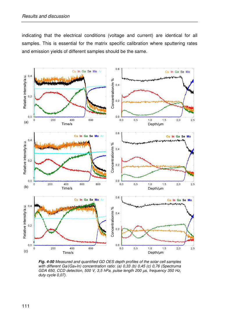
Results and discussion
111
indicating that the electrical conditions (voltage and current) are identical for all
samples. This is essential for the matrix specific calibration where sputtering rates
and emission yields of different samples should be the same.
Fig. 4-50 Measured and quantified GD OES depth profiles of the solar cell samples with different Ga/(Ga+In) concentration ratio: (a) 0,33 (b) 0,45 (c) 0,76 (Spectruma GDA 650, CCD detection, 500 V, 3,5 hPa, pulse length 200 µs, frequency 350 Hz, duty cycle 0,07).
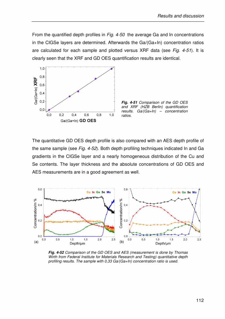
Results and discussion
112
From the quantified depth profiles in Fig. 4-50 the average Ga and In concentrations
in the CIGSe layers are determined. Afterwards the Ga/(Ga+In) concentration ratios
are calculated for each sample and plotted versus XRF data (see Fig. 4-51). It is
clearly seen that the XRF and GD OES quantification results are identical.
Fig. 4-51 Comparison of the GD OES and XRF (HZB Berlin) quantification results. Ga/(Ga+In) – concentration ratios.
The quantitative GD OES depth profile is also compared with an AES depth profile of
the same sample (see Fig. 4-52). Both depth profiling techniques indicated In and Ga
gradients in the CIGSe layer and a nearly homogeneous distribution of the Cu and
Se contents. The layer thickness and the absolute concentrations of GD OES and
AES measurements are in a good agreement as well.
Fig. 4-52 Comparison of the GD OES and AES (measurement is done by Thomas Wirth from Federal Institute for Materials Research and Testing) quantitative depth profiling results. The sample with 0,33 Ga/(Ga+In) concentration ratio is used.
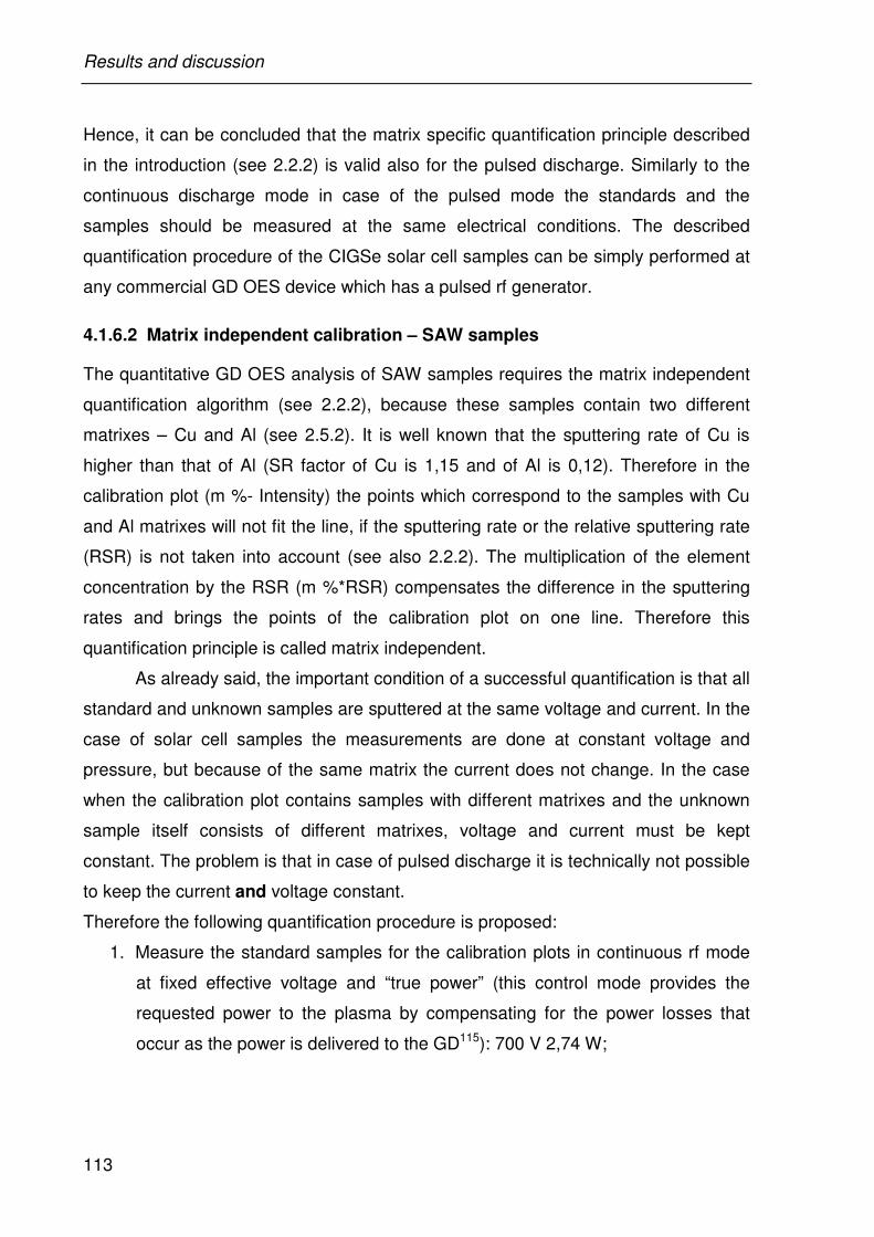
Results and discussion
113
Hence, it can be concluded that the matrix specific quantification principle described
in the introduction (see 2.2.2) is valid also for the pulsed discharge. Similarly to the
continuous discharge mode in case of the pulsed mode the standards and the
samples should be measured at the same electrical conditions. The described
quantification procedure of the CIGSe solar cell samples can be simply performed at
any commercial GD OES device which has a pulsed rf generator.
4.1.6.2 Matrix independent calibration – SAW samples
The quantitative GD OES analysis of SAW samples requires the matrix independent
quantification algorithm (see 2.2.2), because these samples contain two different
matrixes – Cu and Al (see 2.5.2). It is well known that the sputtering rate of Cu is
higher than that of Al (SR factor of Cu is 1,15 and of Al is 0,12). Therefore in the
calibration plot (m %- Intensity) the points which correspond to the samples with Cu
and Al matrixes will not fit the line, if the sputtering rate or the relative sputtering rate
(RSR) is not taken into account (see also 2.2.2). The multiplication of the element
concentration by the RSR (m %*RSR) compensates the difference in the sputtering
rates and brings the points of the calibration plot on one line. Therefore this
quantification principle is called matrix independent.
As already said, the important condition of a successful quantification is that all
standard and unknown samples are sputtered at the same voltage and current. In the
case of solar cell samples the measurements are done at constant voltage and
pressure, but because of the same matrix the current does not change. In the case
when the calibration plot contains samples with different matrixes and the unknown
sample itself consists of different matrixes, voltage and current must be kept
constant. The problem is that in case of pulsed discharge it is technically not possible
to keep the current and voltage constant.
Therefore the following quantification procedure is proposed:
1. Measure the standard samples for the calibration plots in continuous rf mode
at fixed effective voltage and “true power” (this control mode provides the
requested power to the plasma by compensating for the power losses that
occur as the power is delivered to the GD115): 700 V 2,74 W;
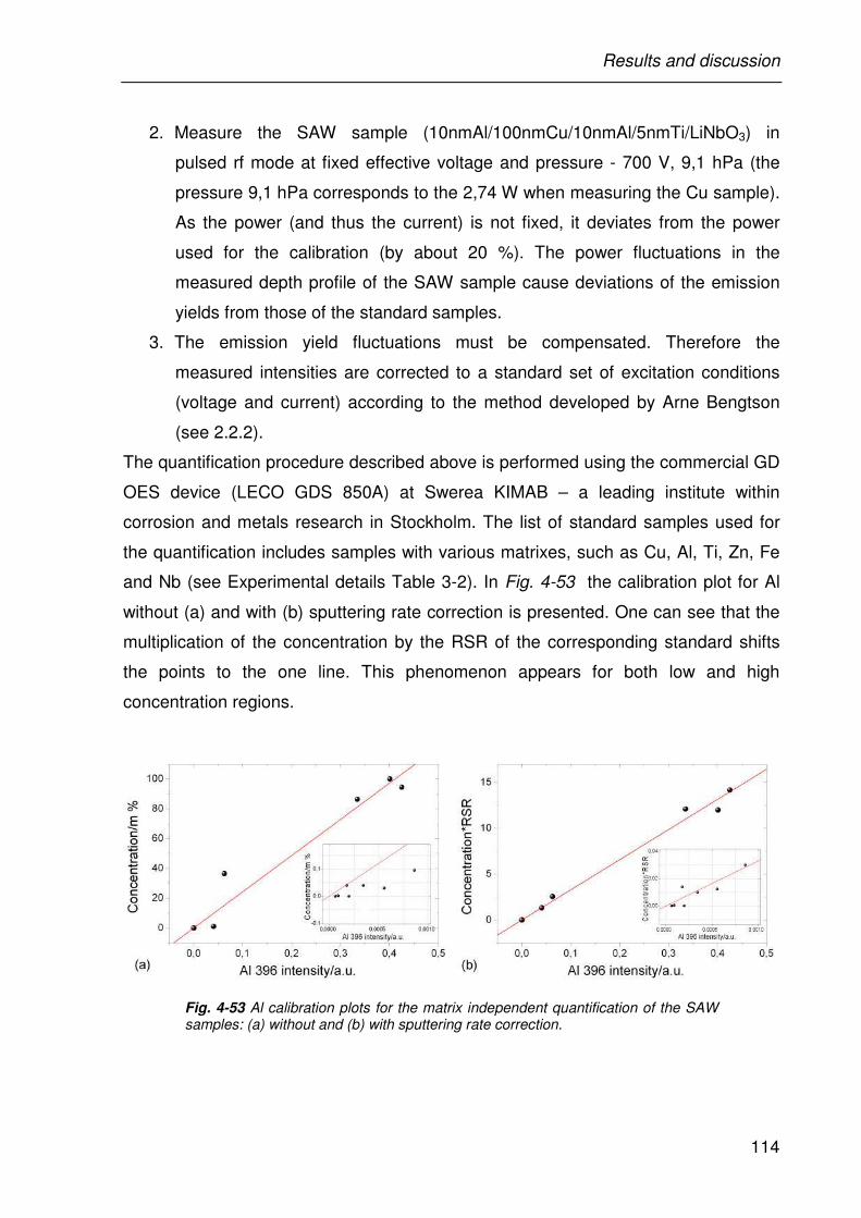
Results and discussion
114
2. Measure the SAW sample (10nmAl/100nmCu/10nmAl/5nmTi/LiNbO3) in
pulsed rf mode at fixed effective voltage and pressure - 700 V, 9,1 hPa (the
pressure 9,1 hPa corresponds to the 2,74 W when measuring the Cu sample).
As the power (and thus the current) is not fixed, it deviates from the power
used for the calibration (by about 20 %). The power fluctuations in the
measured depth profile of the SAW sample cause deviations of the emission
yields from those of the standard samples.
3. The emission yield fluctuations must be compensated. Therefore the
measured intensities are corrected to a standard set of excitation conditions
(voltage and current) according to the method developed by Arne Bengtson
(see 2.2.2).
The quantification procedure described above is performed using the commercial GD
OES device (LECO GDS 850A) at Swerea KIMAB – a leading institute within
corrosion and metals research in Stockholm. The list of standard samples used for
the quantification includes samples with various matrixes, such as Cu, Al, Ti, Zn, Fe
and Nb (see Experimental details Table 3-2). In Fig. 4-53 the calibration plot for Al
without (a) and with (b) sputtering rate correction is presented. One can see that the
multiplication of the concentration by the RSR of the corresponding standard shifts
the points to the one line. This phenomenon appears for both low and high
concentration regions.
Fig. 4-53 Al calibration plots for the matrix independent quantification of the SAW samples: (a) without and (b) with sputtering rate correction.
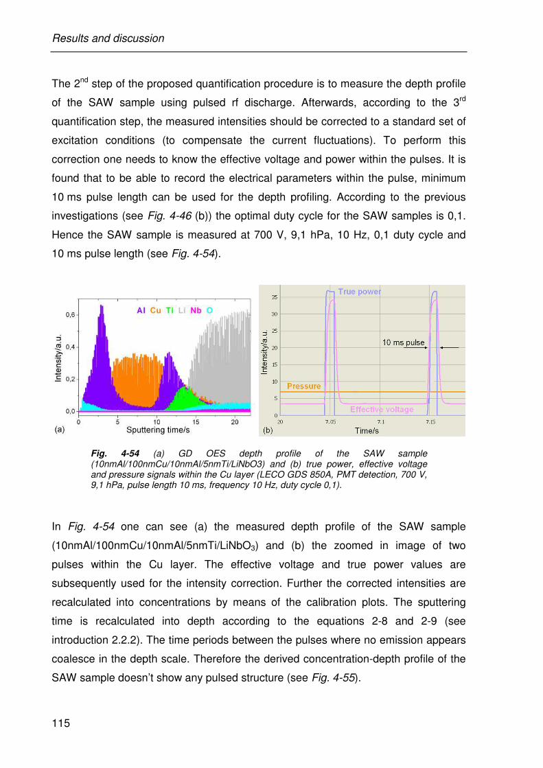
Results and discussion
115
The 2nd step of the proposed quantification procedure is to measure the depth profile
of the SAW sample using pulsed rf discharge. Afterwards, according to the 3rd
quantification step, the measured intensities should be corrected to a standard set of
excitation conditions (to compensate the current fluctuations). To perform this
correction one needs to know the effective voltage and power within the pulses. It is
found that to be able to record the electrical parameters within the pulse, minimum
10 ms pulse length can be used for the depth profiling. According to the previous
investigations (see Fig. 4-46 (b)) the optimal duty cycle for the SAW samples is 0,1.
Hence the SAW sample is measured at 700 V, 9,1 hPa, 10 Hz, 0,1 duty cycle and
10 ms pulse length (see Fig. 4-54).
Fig. 4-54 (a) GD OES depth profile of the SAW sample (10nmAl/100nmCu/10nmAl/5nmTi/LiNbO3) and (b) true power, effective voltage and pressure signals within the Cu layer (LECO GDS 850A, PMT detection, 700 V, 9,1 hPa, pulse length 10 ms, frequency 10 Hz, duty cycle 0,1).
In Fig. 4-54 one can see (a) the measured depth profile of the SAW sample
(10nmAl/100nmCu/10nmAl/5nmTi/LiNbO3) and (b) the zoomed in image of two
pulses within the Cu layer. The effective voltage and true power values are
subsequently used for the intensity correction. Further the corrected intensities are
recalculated into concentrations by means of the calibration plots. The sputtering
time is recalculated into depth according to the equations 2-8 and 2-9 (see
introduction 2.2.2). The time periods between the pulses where no emission appears
coalesce in the depth scale. Therefore the derived concentration-depth profile of the
SAW sample doesn’t show any pulsed structure (see Fig. 4-55).
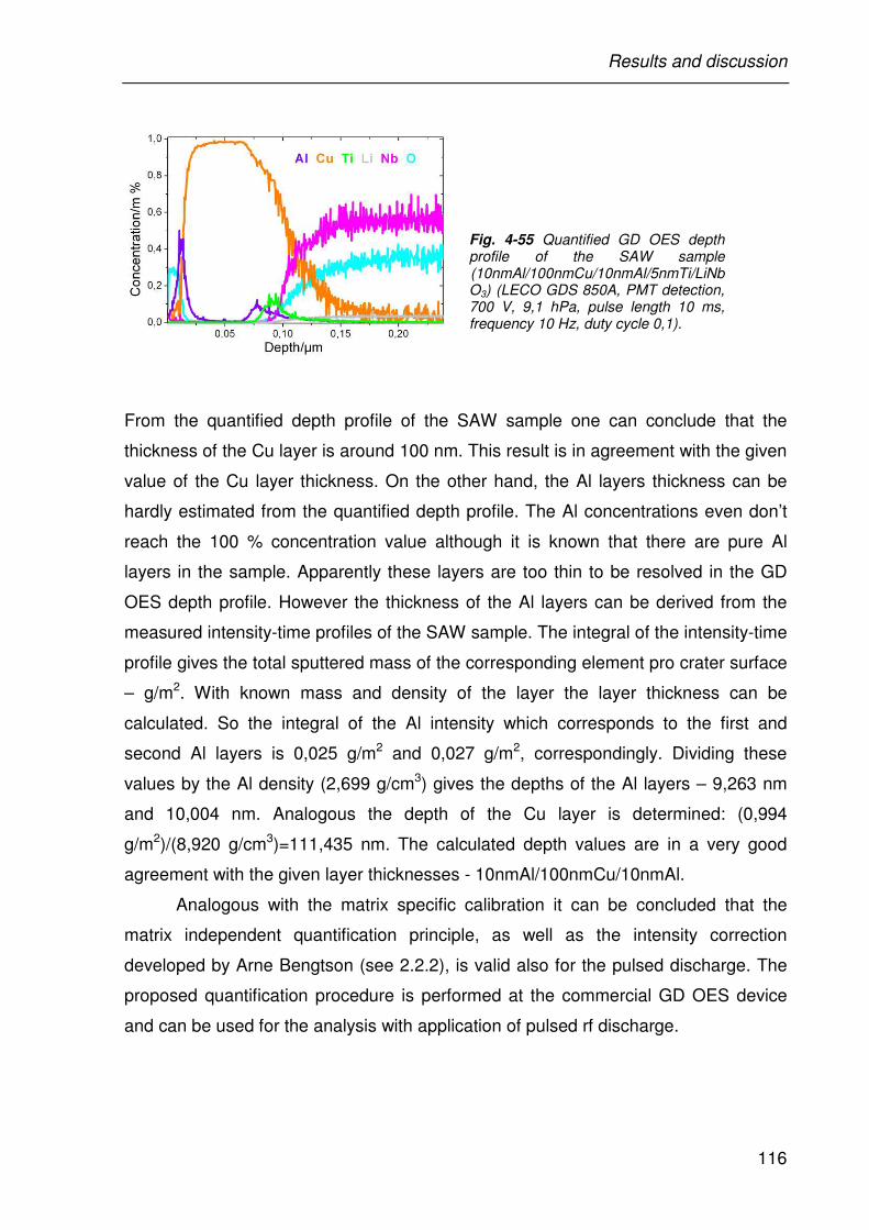
Results and discussion
116
Fig. 4-55 Quantified GD OES depth profile of the SAW sample (10nmAl/100nmCu/10nmAl/5nmTi/LiNbO3) (LECO GDS 850A, PMT detection, 700 V, 9,1 hPa, pulse length 10 ms, frequency 10 Hz, duty cycle 0,1).
From the quantified depth profile of the SAW sample one can conclude that the
thickness of the Cu layer is around 100 nm. This result is in agreement with the given
value of the Cu layer thickness. On the other hand, the Al layers thickness can be
hardly estimated from the quantified depth profile. The Al concentrations even don’t
reach the 100 % concentration value although it is known that there are pure Al
layers in the sample. Apparently these layers are too thin to be resolved in the GD
OES depth profile. However the thickness of the Al layers can be derived from the
measured intensity-time profiles of the SAW sample. The integral of the intensity-time
profile gives the total sputtered mass of the corresponding element pro crater surface
– g/m2. With known mass and density of the layer the layer thickness can be
calculated. So the integral of the Al intensity which corresponds to the first and
second Al layers is 0,025 g/m2 and 0,027 g/m2, correspondingly. Dividing these
values by the Al density (2,699 g/cm3) gives the depths of the Al layers – 9,263 nm
and 10,004 nm. Analogous the depth of the Cu layer is determined: (0,994
g/m2)/(8,920 g/cm3)=111,435 nm. The calculated depth values are in a very good
agreement with the given layer thicknesses - 10nmAl/100nmCu/10nmAl.
Analogous with the matrix specific calibration it can be concluded that the
matrix independent quantification principle, as well as the intensity correction
developed by Arne Bengtson (see 2.2.2), is valid also for the pulsed discharge. The
proposed quantification procedure is performed at the commercial GD OES device
and can be used for the analysis with application of pulsed rf discharge.
Results and discussion
117
4.2 Application of PGD in GD OES analysis
The studies of the PGD described in the previous chapters are relevant for the
application of the GD OES analysis in materials science. In the present chapter some
examples are shown where pulsed GD OES measurements are helpful at the
investigation of the thin film solar cells (TFSC – see 2.5.1) and SAW devices (see
2.5.2).
4.2.1 Layer stacks of CIGSe thin film solar cells
4.2.1.1 Comparison of GD OES with other depth profiling techniques
The layer, which has the greatest influence on the efficiency of TFSC, is the sunlight
absorbing layer CIGSe. The elements in this layer are often distributed
inhomogeneously. As already discussed in the introduction (see 2.5.1) the
composition of the absorber layer may affect the electrical and optoelectrical
properties of thin film devices. Hence the analysis of the elemental distributions in the
thin films is essential for both research and industry. To find the most suitable depth
profiling method for the thin film solar cells several techniques are compared in terms
of their spatial and lateral resolution, speed of measurement, accuracy and
availability. This comparative study is the result of the collaborative work of the
research groups from various European and American institutes, universities and
companies. For the depth profiling analysis all research groups used identical
samples with a 2 µm thick CIGSe layer on a Mo/soda-lime glass substrate with solar-
conversion efficiency of up to 20,1 %. The work is mainly focused on the elemental
distributions of the matrix elements, in particular Cu, In, Ga and Se. The sample
preparation procedure, methods used and results are comprehensively described in
a joint article and book.231,232
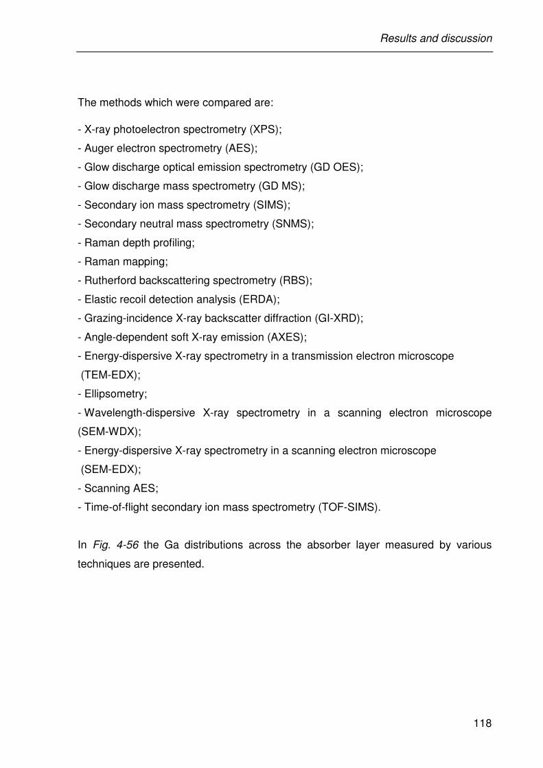
Results and discussion
118
The methods which were compared are:
- X-ray photoelectron spectrometry (XPS);
- Auger electron spectrometry (AES);
- Glow discharge optical emission spectrometry (GD OES);
- Glow discharge mass spectrometry (GD MS);
- Secondary ion mass spectrometry (SIMS);
- Secondary neutral mass spectrometry (SNMS);
- Raman depth profiling;
- Raman mapping;
- Rutherford backscattering spectrometry (RBS);
- Elastic recoil detection analysis (ERDA);
- Grazing-incidence X-ray backscatter diffraction (GI-XRD);
- Angle-dependent soft X-ray emission (AXES);
- Energy-dispersive X-ray spectrometry in a transmission electron microscope
(TEM-EDX);
- Ellipsometry;
- Wavelength-dispersive X-ray spectrometry in a scanning electron microscope
(SEM-WDX);
- Energy-dispersive X-ray spectrometry in a scanning electron microscope
(SEM-EDX);
- Scanning AES;
- Time-of-flight secondary ion mass spectrometry (TOF-SIMS).
In Fig. 4-56 the Ga distributions across the absorber layer measured by various
techniques are presented.
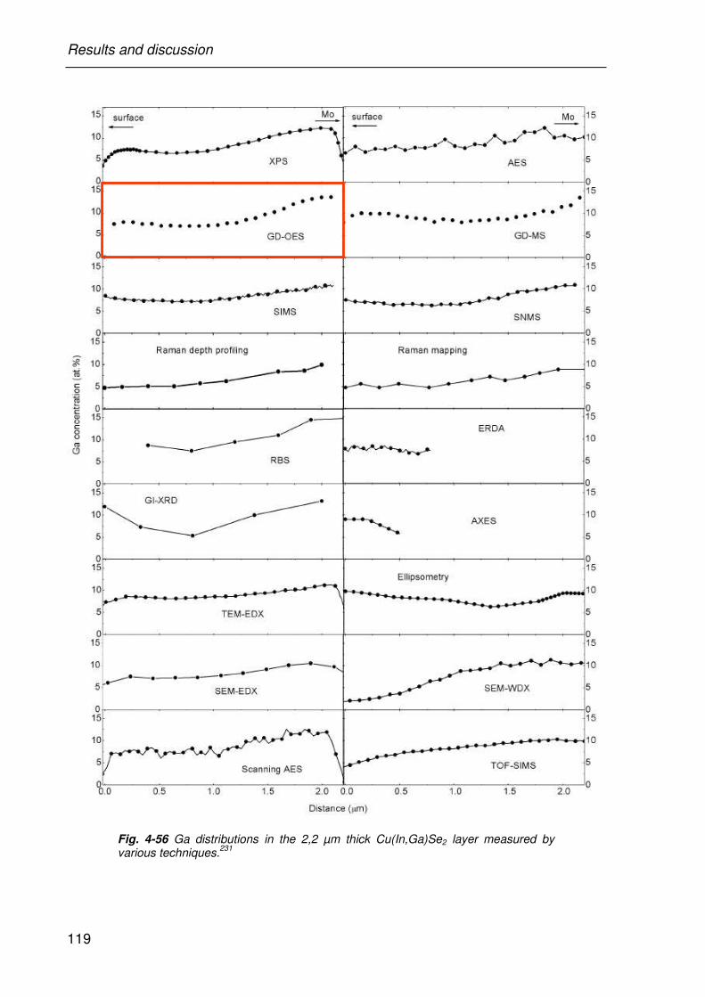
Results and discussion
119
Fig. 4-56 Ga distributions in the 2,2 µm thick Cu(In,Ga)Se2 layer measured by various techniques.
231
Results and discussion
120
Nearly all depth profiling techniques show a similar Ga gradient in the CIGSe layer
with rise of the Ga content close to the absorber/Mo interface. However the question
which technique is the best for depth profiling of solar cells cannot be answered. It is
concluded that there is no method which provides satisfactory quantitative elemental
distributions across the CIGSe layer, because all applied measurement techniques
have their advantages and disadvantages. To select the measurement technique one
needs to specify the requirements to the method and result, such as: destructive or
nondestructive method, matrix or trace elements should be measured, what should
be the depth and spatial resolution, measurement time, cost and availability. To avoid
any ambiguous results it is better to use two or several measurement techniques.
In the joint article of D. Abou-Ras et al. all applied methods are discussed with
respect to their strengths. GD OES along with GD MS are described as methods
which provide the fastest acquisitions (2 µm thick CIGSe layer is analyzed within 5-7
min) and have the possibility to measure the distributions of trace elements. So GD
OES is a technique which can be used in an industrial scale, for example to control
the manufacturing process.231
4.2.1.2 The role of an Al2O3 barrier layer in achieving high efficiency solar cells
on flexible steel substrates
This work belongs to the investigations of the research group from HZB and is
published in the joint paper of Sophie E. Gledhill et al..233 Flexible substrate materials
are attractive for the possibility to make lightweight flexible solar cell devices with
advantages for certain applications, e.g. in space. In addition flexible substrates give
the possibility to deposit the thin-film materials in roll-to-roll processes, which are
potentially cost advantageous.163 One of the substrate materials that has shown
promising results is steel. However to guarantee a good solar cell performance, the
diffusion of Fe from the steel into the CIGSe absorber layer should be prevented, i.e.
a barrier layer between the solar cell stack and the steel substrate is necessary. The
requirements for a good barrier layer are: it should electronically and chemically
isolate the CIGSe and Mo layers from the steel; it should be easily and
homogeneously deposited and cheap. The Al2O3 used in the present work meets
these criteria. GD OES and SIMS depth profiles indicate the efficiency of Al2O3 as
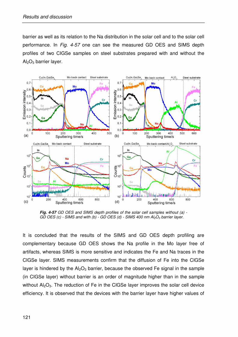
Results and discussion
121
barrier as well as its relation to the Na distribution in the solar cell and to the solar cell
performance. In Fig. 4-57 one can see the measured GD OES and SIMS depth
profiles of two CIGSe samples on steel substrates prepared with and without the
Al2O3 barrier layer.
Fig. 4-57 GD OES and SIMS depth profiles of the solar cell samples without (a) - GD OES (c) - SIMS and with (b) - GD OES (d) - SIMS 400 nm Al2O3 barrier layer.
It is concluded that the results of the SIMS and GD OES depth profiling are
complementary because GD OES shows the Na profile in the Mo layer free of
artifacts, whereas SIMS is more sensitive and indicates the Fe and Na traces in the
CIGSe layer. SIMS measurements confirm that the diffusion of Fe into the CIGSe
layer is hindered by the Al2O3 barrier, because the observed Fe signal in the sample
(in CIGSe layer) without barrier is an order of magnitude higher than in the sample
without Al2O3. The reduction of Fe in the CIGSe layer improves the solar cell device
efficiency. It is observed that the devices with the barrier layer have higher values of
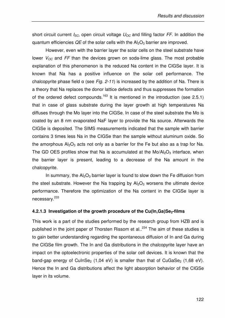
Results and discussion
122
short circuit current ISC, open circuit voltage UOC and filling factor FF. In addition the
quantum efficiencies QE of the solar cells with the Al2O3 barrier are improved.
However, even with the barrier layer the solar cells on the steel substrate have
lower VOC and FF than the devices grown on soda-lime glass. The most probable
explanation of this phenomenon is the reduced Na content in the CIGSe layer. It is
known that Na has a positive influence on the solar cell performance. The
chalcopyrite phase field α (see Fig. 2-11) is increased by the addition of Na. There is
a theory that Na replaces the donor lattice defects and thus suppresses the formation
of the ordered defect compounds.163 It is mentioned in the introduction (see 2.5.1)
that in case of glass substrate during the layer growth at high temperatures Na
diffuses through the Mo layer into the CIGSe. In case of the steel substrate the Mo is
coated by an 8 nm evaporated NaF layer to provide the Na source. Afterwards the
CIGSe is deposited. The SIMS measurements indicated that the sample with barrier
contains 3 times less Na in the CIGSe than the sample without aluminum oxide. So
the amorphous Al2O3 acts not only as a barrier for the Fe but also as a trap for Na.
The GD OES profiles show that Na is accumulated at the Mo/Al2O3 interface, when
the barrier layer is present, leading to a decrease of the Na amount in the
chalcopyrite.
In summary, the Al2O3 barrier layer is found to slow down the Fe diffusion from
the steel substrate. However the Na trapping by Al2O3 worsens the ultimate device
performance. Therefore the optimization of the Na content in the CIGSe layer is
necessary.233
4.2.1.3 Investigation of the growth procedure of the Cu(In,Ga)Se2-films
This work is a part of the studies performed by the research group from HZB and is
published in the joint paper of Thorsten Rissom et al..234 The aim of these studies is
to gain better understanding regarding the spontaneous diffusion of In and Ga during
the CIGSe film growth. The In and Ga distributions in the chalcopyrite layer have an
impact on the optoelectronic properties of the solar cell devices. It is known that the
band-gap energy of CuInSe2 (1,04 eV) is smaller than that of CuGaSe2 (1,68 eV).
Hence the In and Ga distributions affect the light absorption behavior of the CIGSe
layer in its volume.
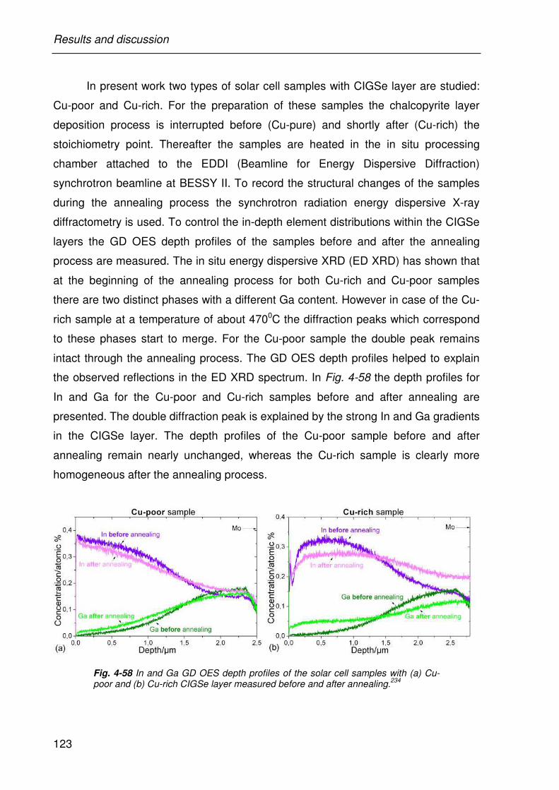
Results and discussion
123
In present work two types of solar cell samples with CIGSe layer are studied:
Cu-poor and Cu-rich. For the preparation of these samples the chalcopyrite layer
deposition process is interrupted before (Cu-pure) and shortly after (Cu-rich) the
stoichiometry point. Thereafter the samples are heated in the in situ processing
chamber attached to the EDDI (Beamline for Energy Dispersive Diffraction)
synchrotron beamline at BESSY II. To record the structural changes of the samples
during the annealing process the synchrotron radiation energy dispersive X-ray
diffractometry is used. To control the in-depth element distributions within the CIGSe
layers the GD OES depth profiles of the samples before and after the annealing
process are measured. The in situ energy dispersive XRD (ED XRD) has shown that
at the beginning of the annealing process for both Cu-rich and Cu-poor samples
there are two distinct phases with a different Ga content. However in case of the Cu-
rich sample at a temperature of about 4700C the diffraction peaks which correspond
to these phases start to merge. For the Cu-poor sample the double peak remains
intact through the annealing process. The GD OES depth profiles helped to explain
the observed reflections in the ED XRD spectrum. In Fig. 4-58 the depth profiles for
In and Ga for the Cu-poor and Cu-rich samples before and after annealing are
presented. The double diffraction peak is explained by the strong In and Ga gradients
in the CIGSe layer. The depth profiles of the Cu-poor sample before and after
annealing remain nearly unchanged, whereas the Cu-rich sample is clearly more
homogeneous after the annealing process.
Fig. 4-58 In and Ga GD OES depth profiles of the solar cell samples with (a) Cu-poor and (b) Cu-rich CIGSe layer measured before and after annealing.
234
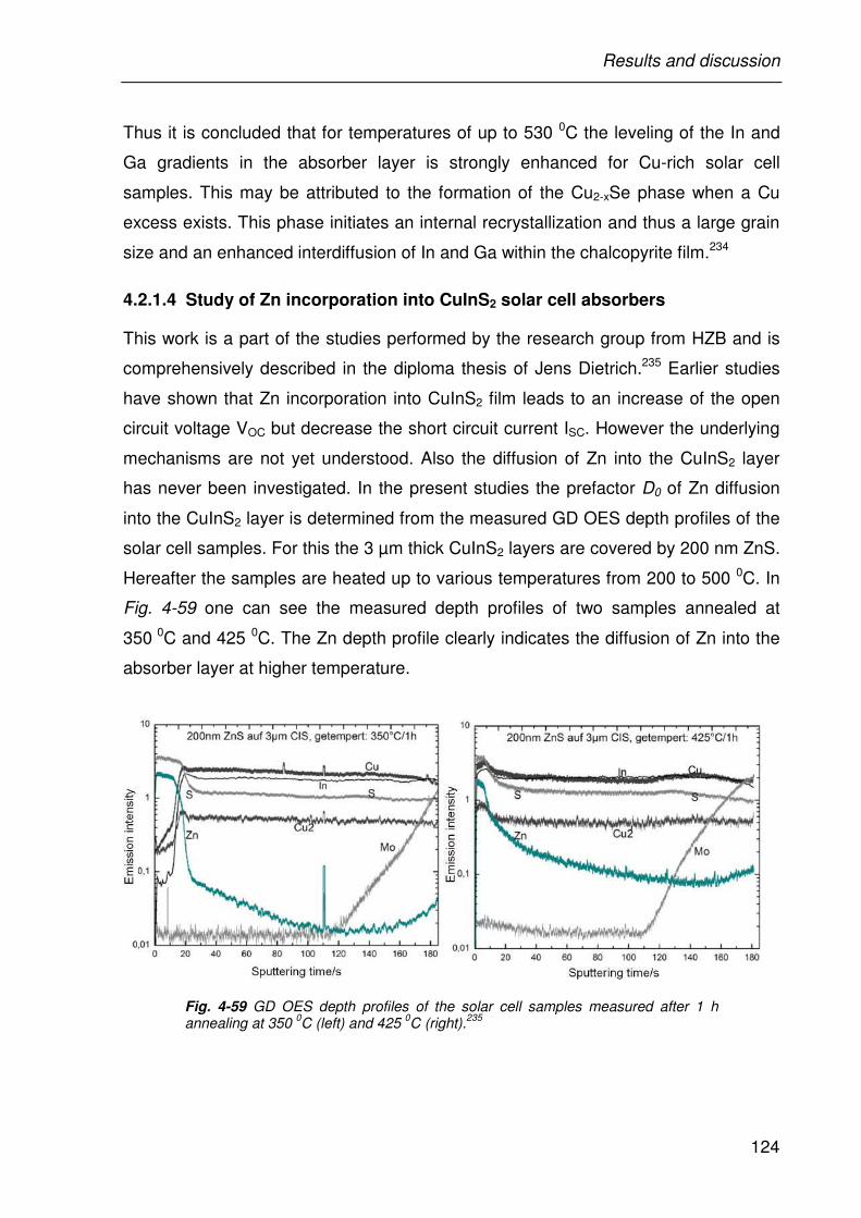
Results and discussion
124
Thus it is concluded that for temperatures of up to 530 0C the leveling of the In and
Ga gradients in the absorber layer is strongly enhanced for Cu-rich solar cell
samples. This may be attributed to the formation of the Cu2-xSe phase when a Cu
excess exists. This phase initiates an internal recrystallization and thus a large grain
size and an enhanced interdiffusion of In and Ga within the chalcopyrite film.234
4.2.1.4 Study of Zn incorporation into CuInS2 solar cell absorbers
This work is a part of the studies performed by the research group from HZB and is
comprehensively described in the diploma thesis of Jens Dietrich.235 Earlier studies
have shown that Zn incorporation into CuInS2 film leads to an increase of the open
circuit voltage VOC but decrease the short circuit current ISC. However the underlying
mechanisms are not yet understood. Also the diffusion of Zn into the CuInS2 layer
has never been investigated. In the present studies the prefactor D0 of Zn diffusion
into the CuInS2 layer is determined from the measured GD OES depth profiles of the
solar cell samples. For this the 3 µm thick CuInS2 layers are covered by 200 nm ZnS.
Hereafter the samples are heated up to various temperatures from 200 to 500 0C. In
Fig. 4-59 one can see the measured depth profiles of two samples annealed at
350 0C and 425 0C. The Zn depth profile clearly indicates the diffusion of Zn into the
absorber layer at higher temperature.
Fig. 4-59 GD OES depth profiles of the solar cell samples measured after 1 h annealing at 350
0C (left) and 425
0C (right).
235
Results and discussion
125
The diffusion coefficients D of Zn into the CuInS2 are determined for each applied
temperature from the corresponding Zn depth profiles using equation 4-1, where c is
Zn concentration; x the depth; t the annealing time and M the molar mass:
2
4
1ln)),(ln( x
DtDt
Mtxc
−+
=
π 4-1
Instead of the logarithm of the concentration the logarithm of the emission intensity
can be applied, because the concentration is linearly proportional to the emission
intensity, when the sputtering rate does not change (see Fig. 4-59 time scale). The
depth x is estimated using the known thicknesses of ZnS and CuInS2 layers. Hence
for the determination of the diffusion coefficients the logarithm of the Zn emission
intensity from the depth profiles measured at different temperatures is plotted versus
the square of the depth (see Fig. 4-60).
Fig. 4-60 Left - GD OES depth profiles of Zn plotted as logarithm of the Zn intensity versus the square of the depth. Right - Arrhenius plot for the determination of the prefactor D0 and the activation energy EA.
235
According to equation 4-1 the diffusion coefficient D can be calculated from the slope
of linear regions of these plots. In this way the D values are deduced and used for
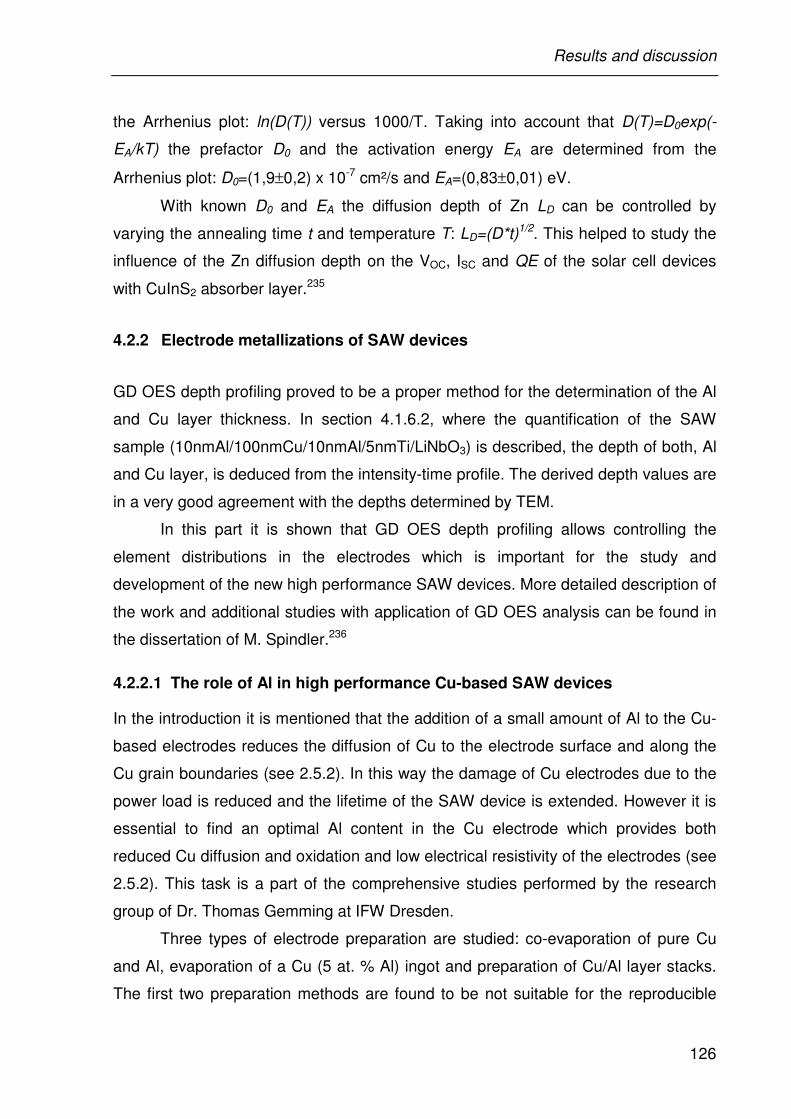
Results and discussion
126
the Arrhenius plot: ln(D(T)) versus 1000/T. Taking into account that D(T)=D0exp(-
EA/kT) the prefactor D0 and the activation energy EA are determined from the
Arrhenius plot: D0=(1,9±0,2) x 10-7 cm²/s and EA=(0,83±0,01) eV.
With known D0 and EA the diffusion depth of Zn LD can be controlled by
varying the annealing time t and temperature T: LD=(D*t)1/2. This helped to study the
influence of the Zn diffusion depth on the VOC, ISC and QE of the solar cell devices
with CuInS2 absorber layer.235
4.2.2 Electrode metallizations of SAW devices
GD OES depth profiling proved to be a proper method for the determination of the Al
and Cu layer thickness. In section 4.1.6.2, where the quantification of the SAW
sample (10nmAl/100nmCu/10nmAl/5nmTi/LiNbO3) is described, the depth of both, Al
and Cu layer, is deduced from the intensity-time profile. The derived depth values are
in a very good agreement with the depths determined by TEM.
In this part it is shown that GD OES depth profiling allows controlling the
element distributions in the electrodes which is important for the study and
development of the new high performance SAW devices. More detailed description of
the work and additional studies with application of GD OES analysis can be found in
the dissertation of M. Spindler.236
4.2.2.1 The role of Al in high performance Cu-based SAW devices
In the introduction it is mentioned that the addition of a small amount of Al to the Cu-
based electrodes reduces the diffusion of Cu to the electrode surface and along the
Cu grain boundaries (see 2.5.2). In this way the damage of Cu electrodes due to the
power load is reduced and the lifetime of the SAW device is extended. However it is
essential to find an optimal Al content in the Cu electrode which provides both
reduced Cu diffusion and oxidation and low electrical resistivity of the electrodes (see
2.5.2). This task is a part of the comprehensive studies performed by the research
group of Dr. Thomas Gemming at IFW Dresden.
Three types of electrode preparation are studied: co-evaporation of pure Cu
and Al, evaporation of a Cu (5 at. % Al) ingot and preparation of Cu/Al layer stacks.
The first two preparation methods are found to be not suitable for the reproducible
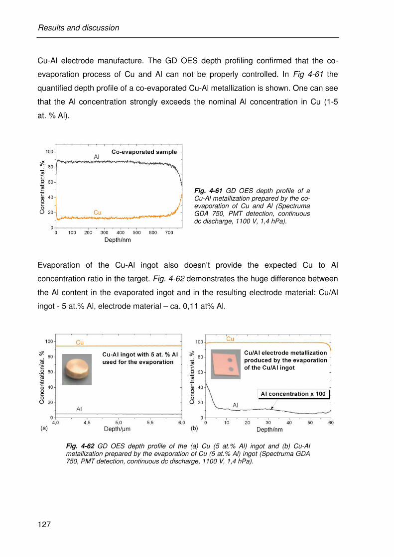
Results and discussion
127
Cu-Al electrode manufacture. The GD OES depth profiling confirmed that the co-
evaporation process of Cu and Al can not be properly controlled. In Fig 4-61 the
quantified depth profile of a co-evaporated Cu-Al metallization is shown. One can see
that the Al concentration strongly exceeds the nominal Al concentration in Cu (1-5
at. % Al).
Fig. 4-61 GD OES depth profile of a Cu-Al metallization prepared by the co-evaporation of Cu and Al (Spectruma GDA 750, PMT detection, continuous dc discharge, 1100 V, 1,4 hPa).
Evaporation of the Cu-Al ingot also doesn’t provide the expected Cu to Al
concentration ratio in the target. Fig. 4-62 demonstrates the huge difference between
the Al content in the evaporated ingot and in the resulting electrode material: Cu/Al
ingot - 5 at.% Al, electrode material – ca. 0,11 at% Al.
Fig. 4-62 GD OES depth profile of the (a) Cu (5 at.% Al) ingot and (b) Cu-Al metallization prepared by the evaporation of Cu (5 at.% Al) ingot (Spectruma GDA 750, PMT detection, continuous dc discharge, 1100 V, 1,4 hPa).
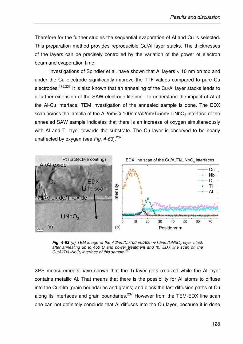
Results and discussion
128
Therefore for the further studies the sequential evaporation of Al and Cu is selected.
This preparation method provides reproducible Cu/Al layer stacks. The thicknesses
of the layers can be precisely controlled by the variation of the power of electron
beam and evaporation time.
Investigations of Spindler et al. have shown that Al layers < 10 nm on top and
under the Cu electrode significantly improve the TTF values compared to pure Cu
electrodes.175,237 It is also known that an annealing of the Cu/Al layer stacks leads to
a further extension of the SAW electrode lifetime. To understand the impact of Al at
the Al-Cu interface, TEM investigation of the annealed sample is done. The EDX
scan across the lamella of the Al2nm/Cu100nm/Al2nm/Ti5nm/ LiNbO3 interface of the
annealed SAW sample indicates that there is an increase of oxygen simultaneously
with Al and Ti layer towards the substrate. The Cu layer is observed to be nearly
unaffected by oxygen (see Fig. 4-63).237
Fig. 4-63 (a) TEM image of the Al2nm/Cu100nm/Al2nm/Ti5nm/LiNbO3 layer stack after annealing up to 450°C and power treatment and (b) EDX line scan on the Cu/Al/Ti/LiNbO3 interface of this sample.
237
XPS measurements have shown that the Ti layer gets oxidized while the Al layer
contains metallic Al. That means that there is the possibility for Al atoms to diffuse
into the Cu-film (grain boundaries and grains) and block the fast diffusion paths of Cu
along its interfaces and grain boundaries.237 However from the TEM-EDX line scan
one can not definitely conclude that Al diffuses into the Cu layer, because it is done
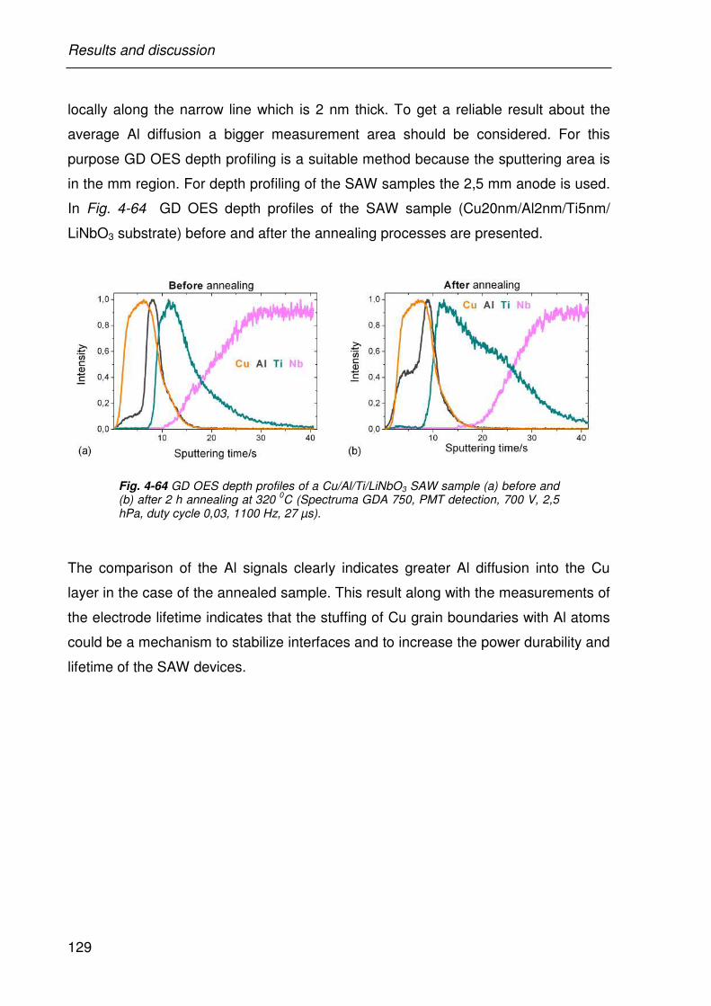
Results and discussion
129
locally along the narrow line which is 2 nm thick. To get a reliable result about the
average Al diffusion a bigger measurement area should be considered. For this
purpose GD OES depth profiling is a suitable method because the sputtering area is
in the mm region. For depth profiling of the SAW samples the 2,5 mm anode is used.
In Fig. 4-64 GD OES depth profiles of the SAW sample (Cu20nm/Al2nm/Ti5nm/
LiNbO3 substrate) before and after the annealing processes are presented.
Fig. 4-64 GD OES depth profiles of a Cu/Al/Ti/LiNbO3 SAW sample (a) before and (b) after 2 h annealing at 320
0C (Spectruma GDA 750, PMT detection, 700 V, 2,5
hPa, duty cycle 0,03, 1100 Hz, 27 µs).
The comparison of the Al signals clearly indicates greater Al diffusion into the Cu
layer in the case of the annealed sample. This result along with the measurements of
the electrode lifetime indicates that the stuffing of Cu grain boundaries with Al atoms
could be a mechanism to stabilize interfaces and to increase the power durability and
lifetime of the SAW devices.
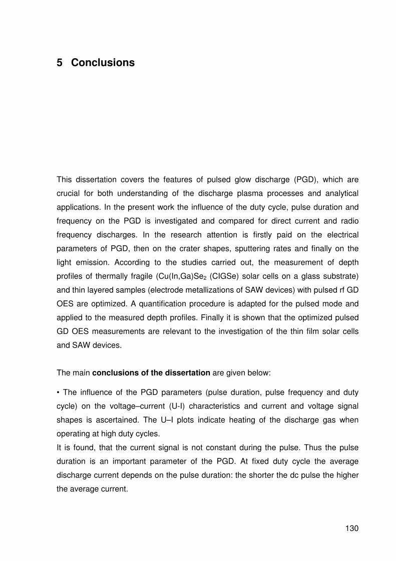
130
5 Conclusions
This dissertation covers the features of pulsed glow discharge (PGD), which are
crucial for both understanding of the discharge plasma processes and analytical
applications. In the present work the influence of the duty cycle, pulse duration and
frequency on the PGD is investigated and compared for direct current and radio
frequency discharges. In the research attention is firstly paid on the electrical
parameters of PGD, then on the crater shapes, sputtering rates and finally on the
light emission. According to the studies carried out, the measurement of depth
profiles of thermally fragile (Cu(In,Ga)Se2 (CIGSe) solar cells on a glass substrate)
and thin layered samples (electrode metallizations of SAW devices) with pulsed rf GD
OES are optimized. A quantification procedure is adapted for the pulsed mode and
applied to the measured depth profiles. Finally it is shown that the optimized pulsed
GD OES measurements are relevant to the investigation of the thin film solar cells
and SAW devices.
The main conclusions of the dissertation are given below:
• The influence of the PGD parameters (pulse duration, pulse frequency and duty
cycle) on the voltage–current (U-I) characteristics and current and voltage signal
shapes is ascertained. The U–I plots indicate heating of the discharge gas when
operating at high duty cycles.
It is found, that the current signal is not constant during the pulse. Thus the pulse
duration is an important parameter of the PGD. At fixed duty cycle the average
discharge current depends on the pulse duration: the shorter the dc pulse the higher
the average current.
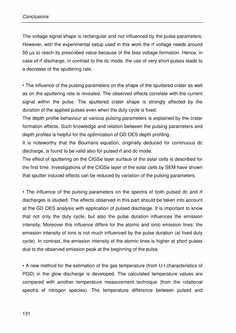
Conclusions
131
The voltage signal shape is rectangular and not influenced by the pulse parameters.
However, with the experimental setup used in this work the rf voltage needs around
50 µs to reach its prescribed value because of the bias voltage formation. Hence, in
case of rf discharge, in contrast to the dc mode, the use of very short pulses leads to
a decrease of the sputtering rate.
• The influence of the pulsing parameters on the shape of the sputtered crater as well
as on the sputtering rate is revealed. The observed effects correlate with the current
signal within the pulse. The sputtered crater shape is strongly affected by the
duration of the applied pulses even when the duty cycle is fixed.
The depth profile behaviour at various pulsing parameters is explained by the crater
formation effects. Such knowledge and relation between the pulsing parameters and
depth profiles is helpful for the optimization of GD OES depth profiling.
It is noteworthy that the Boumans equation, originally deduced for continuous dc
discharge, is found to be valid also for pulsed rf and dc mode.
The effect of sputtering on the CIGSe layer surface of the solar cells is described for
the first time. Investigations of the CIGSe layer of the solar cells by SEM have shown
that sputter induced effects can be reduced by variation of the pulsing parameters.
• The influence of the pulsing parameters on the spectra of both pulsed dc and rf
discharges is studied. The effects observed in this part should be taken into account
at the GD OES analysis with application of pulsed discharge. It is important to know
that not only the duty cycle, but also the pulse duration influences the emission
intensity. Moreover this influence differs for the atomic and ionic emission lines: the
emission intensity of ions is not much influenced by the pulse duration (at fixed duty
cycle). In contrast, the emission intensity of the atomic lines is higher at short pulses
due to the observed emission peak at the beginning of the pulse.
• A new method for the estimation of the gas temperature (from U-I characteristics of
PGD) in the glow discharge is developed. The calculated temperature values are
compared with another temperature measurement technique (from the rotational
spectra of nitrogen species). The temperature difference between pulsed and
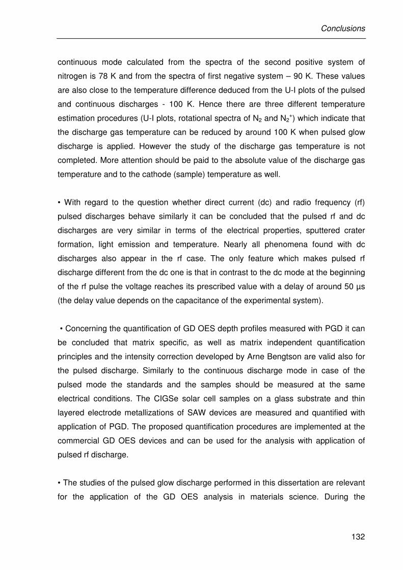
Conclusions
132
continuous mode calculated from the spectra of the second positive system of
nitrogen is 78 K and from the spectra of first negative system – 90 K. These values
are also close to the temperature difference deduced from the U-I plots of the pulsed
and continuous discharges - 100 K. Hence there are three different temperature
estimation procedures (U-I plots, rotational spectra of N2 and N2+) which indicate that
the discharge gas temperature can be reduced by around 100 K when pulsed glow
discharge is applied. However the study of the discharge gas temperature is not
completed. More attention should be paid to the absolute value of the discharge gas
temperature and to the cathode (sample) temperature as well.
• With regard to the question whether direct current (dc) and radio frequency (rf)
pulsed discharges behave similarly it can be concluded that the pulsed rf and dc
discharges are very similar in terms of the electrical properties, sputtered crater
formation, light emission and temperature. Nearly all phenomena found with dc
discharges also appear in the rf case. The only feature which makes pulsed rf
discharge different from the dc one is that in contrast to the dc mode at the beginning
of the rf pulse the voltage reaches its prescribed value with a delay of around 50 µs
(the delay value depends on the capacitance of the experimental system).
• Concerning the quantification of GD OES depth profiles measured with PGD it can
be concluded that matrix specific, as well as matrix independent quantification
principles and the intensity correction developed by Arne Bengtson are valid also for
the pulsed discharge. Similarly to the continuous discharge mode in case of the
pulsed mode the standards and the samples should be measured at the same
electrical conditions. The CIGSe solar cell samples on a glass substrate and thin
layered electrode metallizations of SAW devices are measured and quantified with
application of PGD. The proposed quantification procedures are implemented at the
commercial GD OES devices and can be used for the analysis with application of
pulsed rf discharge.
• The studies of the pulsed glow discharge performed in this dissertation are relevant
for the application of the GD OES analysis in materials science. During the
Conclusions
133
collaborative work with Helmholtz-Zentrum Berlin für Materialien und Energie and
with the research group of Dr. Thomas Gemming at IFW Dresden the optimized
pulsed GD OES measurements could be successfully applied at the investigation of
thin film solar cells with CIGSe light absorbing layer and electrode metallizations of
SAW devices. In case of the solar cell samples pulsed GD OES depth profiling along
with SIMS measurements reveal the role of the Al2O3 barrier layer in high efficiency
solar cells consisting of a CIGSe/Mo layer stack on a flexible steel substrate (the
barrier layer is between the Mo and steel substrate to prevent the Fe diffusion). The
features of the CIGSe film growth are studied with help of pulsed GD OES and in situ
synchrotron XRD measurements. The diffusion coefficient of Zn into the CuInS2 layer
is determined for the first time from the measured GD OES depth profiles of the
corresponding solar cell samples. In case of SAW samples pulsed GD OES
measurements helped to evaluate the different SAW electrode preparation
procedures and to choose the most suitable one. In addition pulsed GD OES depth
profiling along with XPS, TEM-EDX and electrode lifetime measurements indicates
the possible mechanism of power durability and lifetime improvement of the SAW
devices when small amount of Al is added to the Cu-based electrodes.
The GD OES depth profiling of the solar cell samples is compared with various
depth profiling techniques. It is concluded that there is no perfect depth profiling
method which provides satisfactory elemental distributions across the CIGSe layer
because all applied measurement techniques have their advantages and
disadvantages. However with the knowledge earned in the course of the present
dissertation the pulsed GD OES depth profiling became a useful method
complementing the other analytical techniques.

134
Bibliography
1. F. Paschen, Ann.Phys.u.Chem., 1889, 37, 69.
2. Y. P. Raizer, Gas discharge physics, ed. J. E. Allen, Springer, 1 edition, 1991.
3. H. A. Hyman, Phys Rev, 1979, 20, 855.
4. G. Franz, Kalte Plasmen - Grundlagen, Erscheinungen, Anwendungen, Springer-Verlag Berlin Heidelberg, 1990.
5. A. von Engel, Ionized gases, Clarendon press, Oxford, 1955, 8, pp. 190-228.
6. K. Wagatsuma, in Glow Discharge Optical Emission Spectrometry, ed. R. Payling, D. Jones and A. Bengtson, John Wiley & Sons, Chichester, New York, Weinheim, Brisbane, Singapore, Toronto, 1997, 4.1, pp. 166-175.
7. D. Fang, K. R. Marcus, in Glow Discharge Spectroscopies, ed. K. R. Marcus, 1993, 2, pp. 17-63.
8. A. Bogaerts, J.Anal.At.Spectrom., 2007, 22, 13.
9. B. Chapman, Glow Discharge Processes - Sputtering and Plasma Etching, John Wiley & Sons, 1980.
10. A. Bogaerts, R. Gijbels, J.Anal.At.Spectrom., 1998, 13, 945.
11. A. Bogaerts, R. Gijbels, Spectrochim.Acta B, 1998, 53, 1.
12. A. Bogaerts, R. Gijbels, Plasma Physics Reports, 1998, 24, 573.
13. C. R. Brundle, Jr. Evans, S. Wilson, Encylopedia of Materials Characterization, Butterworth - Heinemann, 1991.
14. K. Slickers, Die automatische Atom-Emissions-Spektralanalyse, Brühlsche Universitätsdruckerei, Gießen, 2, 1992.
15. D. Briggs, M. P. Seah, Practical surface analysis Volume 2 - Ion and Neutral Spectroscopy, Wiley, Chichester, 1992.
16. S. Hofmann, in Practical Surface Analysis, Volume 1 - Auger and X-Ray Photoelectron Spectroscopy, ed. D. Briggs and M. P. Seah, Wiley, Chichester, 1990, pp. 143-200.
17. D. A. Cremers, L. J. Radziemski, Handbook of Laser-Induced Breakdown Spectroscopy, John Wiley & Sons, London, 2006.
18. J. S. Becker, A. Gorbunov, M. Zoriy, A. Izmer, M. Kayser, J.Anal.At.Spectrom., 2006, 21, 19.
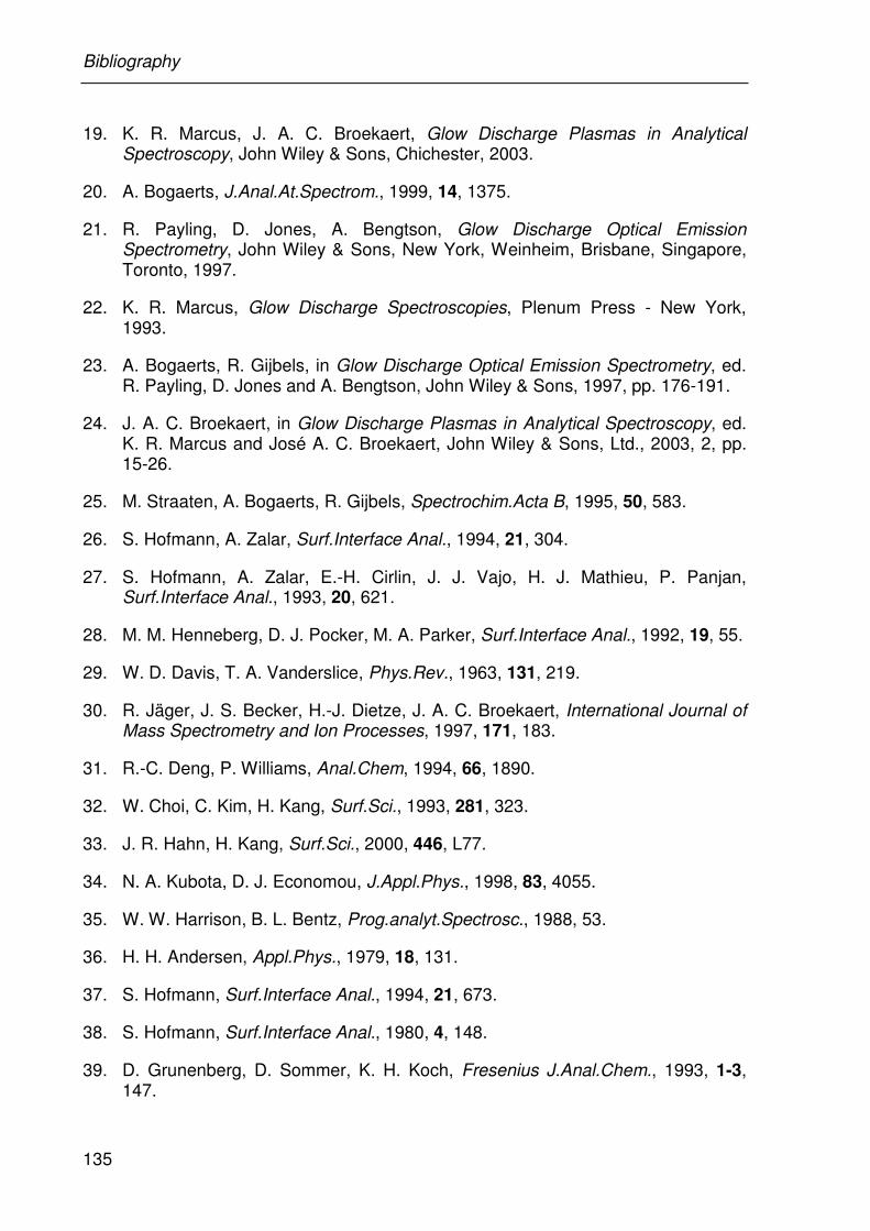
Bibliography
135
19. K. R. Marcus, J. A. C. Broekaert, Glow Discharge Plasmas in Analytical Spectroscopy, John Wiley & Sons, Chichester, 2003.
20. A. Bogaerts, J.Anal.At.Spectrom., 1999, 14, 1375.
21. R. Payling, D. Jones, A. Bengtson, Glow Discharge Optical Emission Spectrometry, John Wiley & Sons, New York, Weinheim, Brisbane, Singapore, Toronto, 1997.
22. K. R. Marcus, Glow Discharge Spectroscopies, Plenum Press - New York, 1993.
23. A. Bogaerts, R. Gijbels, in Glow Discharge Optical Emission Spectrometry, ed. R. Payling, D. Jones and A. Bengtson, John Wiley & Sons, 1997, pp. 176-191.
24. J. A. C. Broekaert, in Glow Discharge Plasmas in Analytical Spectroscopy, ed. K. R. Marcus and José A. C. Broekaert, John Wiley & Sons, Ltd., 2003, 2, pp. 15-26.
25. M. Straaten, A. Bogaerts, R. Gijbels, Spectrochim.Acta B, 1995, 50, 583.
26. S. Hofmann, A. Zalar, Surf.Interface Anal., 1994, 21, 304.
27. S. Hofmann, A. Zalar, E.-H. Cirlin, J. J. Vajo, H. J. Mathieu, P. Panjan, Surf.Interface Anal., 1993, 20, 621.
28. M. M. Henneberg, D. J. Pocker, M. A. Parker, Surf.Interface Anal., 1992, 19, 55.
29. W. D. Davis, T. A. Vanderslice, Phys.Rev., 1963, 131, 219.
30. R. Jäger, J. S. Becker, H.-J. Dietze, J. A. C. Broekaert, International Journal of Mass Spectrometry and Ion Processes, 1997, 171, 183.
31. R.-C. Deng, P. Williams, Anal.Chem, 1994, 66, 1890.
32. W. Choi, C. Kim, H. Kang, Surf.Sci., 1993, 281, 323.
33. J. R. Hahn, H. Kang, Surf.Sci., 2000, 446, L77.
34. N. A. Kubota, D. J. Economou, J.Appl.Phys., 1998, 83, 4055.
35. W. W. Harrison, B. L. Bentz, Prog.analyt.Spectrosc., 1988, 53.
36. H. H. Andersen, Appl.Phys., 1979, 18, 131.
37. S. Hofmann, Surf.Interface Anal., 1994, 21, 673.
38. S. Hofmann, Surf.Interface Anal., 1980, 4, 148.
39. D. Grunenberg, D. Sommer, K. H. Koch, Fresenius J.Anal.Chem., 1993, 1-3, 147.
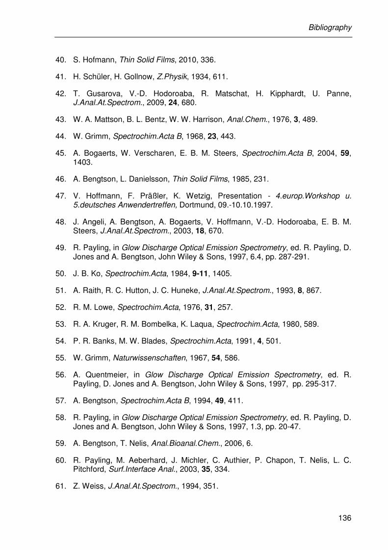
Bibliography
136
40. S. Hofmann, Thin Solid Films, 2010, 336.
41. H. Schüler, H. Gollnow, Z.Physik, 1934, 611.
42. T. Gusarova, V.-D. Hodoroaba, R. Matschat, H. Kipphardt, U. Panne, J.Anal.At.Spectrom., 2009, 24, 680.
43. W. A. Mattson, B. L. Bentz, W. W. Harrison, Anal.Chem., 1976, 3, 489.
44. W. Grimm, Spectrochim.Acta B, 1968, 23, 443.
45. A. Bogaerts, W. Verscharen, E. B. M. Steers, Spectrochim.Acta B, 2004, 59, 1403.
46. A. Bengtson, L. Danielsson, Thin Solid Films, 1985, 231.
47. V. Hoffmann, F. Präßler, K. Wetzig, Presentation - 4.europ.Workshop u. 5.deutsches Anwendertreffen, Dortmund, 09.-10.10.1997.
48. J. Angeli, A. Bengtson, A. Bogaerts, V. Hoffmann, V.-D. Hodoroaba, E. B. M. Steers, J.Anal.At.Spectrom., 2003, 18, 670.
49. R. Payling, in Glow Discharge Optical Emission Spectrometry, ed. R. Payling, D. Jones and A. Bengtson, John Wiley & Sons, 1997, 6.4, pp. 287-291.
50. J. B. Ko, Spectrochim.Acta, 1984, 9-11, 1405.
51. A. Raith, R. C. Hutton, J. C. Huneke, J.Anal.At.Spectrom., 1993, 8, 867.
52. R. M. Lowe, Spectrochim.Acta, 1976, 31, 257.
53. R. A. Kruger, R. M. Bombelka, K. Laqua, Spectrochim.Acta, 1980, 589.
54. P. R. Banks, M. W. Blades, Spectrochim.Acta, 1991, 4, 501.
55. W. Grimm, Naturwissenschaften, 1967, 54, 586.
56. A. Quentmeier, in Glow Discharge Optical Emission Spectrometry, ed. R. Payling, D. Jones and A. Bengtson, John Wiley & Sons, 1997, pp. 295-317.
57. A. Bengtson, Spectrochim.Acta B, 1994, 49, 411.
58. R. Payling, in Glow Discharge Optical Emission Spectrometry, ed. R. Payling, D. Jones and A. Bengtson, John Wiley & Sons, 1997, 1.3, pp. 20-47.
59. A. Bengtson, T. Nelis, Anal.Bioanal.Chem., 2006, 6.
60. R. Payling, M. Aeberhard, J. Michler, C. Authier, P. Chapon, T. Nelis, L. C. Pitchford, Surf.Interface Anal., 2003, 35, 334.
61. Z. Weiss, J.Anal.At.Spectrom., 1994, 351.
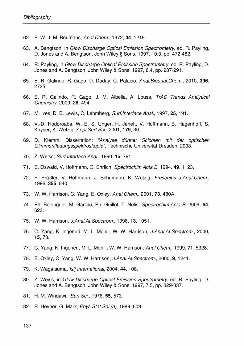
Bibliography
137
62. P. W. J. M. Boumans, Anal.Chem., 1972, 44, 1219.
63. A. Bengtson, in Glow Discharge Optical Emission Spectrometry, ed. R. Payling, D. Jones and A. Bengtson, John Wiley § Sons, 1997, 10.3, pp. 472-482.
64. R. Payling, in Glow Discharge Optical Emission Spectrometry, ed. R. Payling, D. Jones and A. Bengtson, John Wiley & Sons, 1997, 6.4, pp. 287-291.
65. E. R. Galindo, R. Gago, D. Duday, C. Palacio, Anal.Bioanal.Chem., 2010, 396, 2725.
66. E. R. Galindo, R. Gago, J. M. Albella, A. Lousa, TrAC Trends Analytical Chemistry, 2009, 28, 494.
67. M. Ives, D. B. Lewis, C. Lehmberg, Surf.Interface Anal., 1997, 25, 191.
68. V.-D. Hodoroaba, W. E. S. Unger, H. Jenett, V. Hoffmann, B. Hagenhoff, S. Kayser, K. Wetzig, Appl.Surf.Sci., 2001, 179, 30.
69. D. Klemm, Dissertation: "Analyse dünner Scichten mit der optischen Glimmentladungsspektroskopie", Technische Universität Dresden, 2008.
70. Z. Weiss, Surf.Interface Anal., 1990, 15, 791.
71. S. Oswald, V. Hoffmann, G. Ehrlich, Spectrochim.Acta B, 1994, 49, 1123.
72. F. Präßler, V. Hoffmann, J. Schumann, K. Wetzig, Fresenius J.Anal.Chem., 1996, 355, 840.
73. W. W. Harrison, C. Yang, E. Oxley, Anal.Chem., 2001, 73, 480A.
74. Ph. Belenguer, M. Ganciu, Ph. Guillot, T. Nelis, Spectrochim.Acta B, 2009, 64, 623.
75. W. W. Harrison, J.Anal.At.Spectrom., 1998, 13, 1051.
76. C. Yang, K. Ingeneri, M. L. Mohill, W. W. Harrison, J.Anal.At.Spectrom., 2000, 15, 73.
77. C. Yang, K. Ingeneri, M. L. Mohill, W. W. Harrison, Anal.Chem., 1999, 71, 5328.
78. E. Oxley, C. Yang, W. W. Harrison, J.Anal.At.Spectrom., 2000, 9, 1241.
79. K. Wagatsuma, Isij International, 2004, 44, 108.
80. Z. Weiss, in Glow Discharge Optical Emission Spectrometry, ed. R. Payling, D. Jones and A. Bengtson, John Wiley & Sons, 1997, 7.5, pp. 329-337.
81. H. M. Windawi, Surf.Sci., 1976, 55, 573.
82. R. Heyner, G. Marx, Phys.Stat.Sol.(a), 1989, 609.
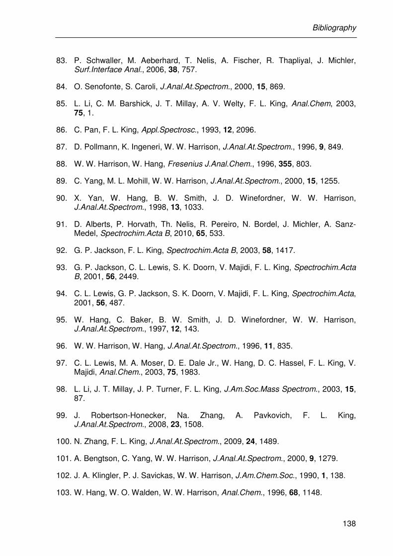
Bibliography
138
83. P. Schwaller, M. Aeberhard, T. Nelis, A. Fischer, R. Thapliyal, J. Michler, Surf.Interface Anal., 2006, 38, 757.
84. O. Senofonte, S. Caroli, J.Anal.At.Spectrom., 2000, 15, 869.
85. L. Li, C. M. Barshick, J. T. Millay, A. V. Welty, F. L. King, Anal.Chem, 2003, 75, 1.
86. C. Pan, F. L. King, Appl.Spectrosc., 1993, 12, 2096.
87. D. Pollmann, K. Ingeneri, W. W. Harrison, J.Anal.At.Spectrom., 1996, 9, 849.
88. W. W. Harrison, W. Hang, Fresenius J.Anal.Chem., 1996, 355, 803.
89. C. Yang, M. L. Mohill, W. W. Harrison, J.Anal.At.Spectrom., 2000, 15, 1255.
90. X. Yan, W. Hang, B. W. Smith, J. D. Winefordner, W. W. Harrison, J.Anal.At.Spectrom., 1998, 13, 1033.
91. D. Alberts, P. Horvath, Th. Nelis, R. Pereiro, N. Bordel, J. Michler, A. Sanz-Medel, Spectrochim.Acta B, 2010, 65, 533.
92. G. P. Jackson, F. L. King, Spectrochim.Acta B, 2003, 58, 1417.
93. G. P. Jackson, C. L. Lewis, S. K. Doorn, V. Majidi, F. L. King, Spectrochim.Acta B, 2001, 56, 2449.
94. C. L. Lewis, G. P. Jackson, S. K. Doorn, V. Majidi, F. L. King, Spectrochim.Acta, 2001, 56, 487.
95. W. Hang, C. Baker, B. W. Smith, J. D. Winefordner, W. W. Harrison, J.Anal.At.Spectrom., 1997, 12, 143.
96. W. W. Harrison, W. Hang, J.Anal.At.Spectrom., 1996, 11, 835.
97. C. L. Lewis, M. A. Moser, D. E. Dale Jr., W. Hang, D. C. Hassel, F. L. King, V. Majidi, Anal.Chem., 2003, 75, 1983.
98. L. Li, J. T. Millay, J. P. Turner, F. L. King, J.Am.Soc.Mass Spectrom., 2003, 15, 87.
99. J. Robertson-Honecker, Na. Zhang, A. Pavkovich, F. L. King, J.Anal.At.Spectrom., 2008, 23, 1508.
100. N. Zhang, F. L. King, J.Anal.At.Spectrom., 2009, 24, 1489.
101. A. Bengtson, C. Yang, W. W. Harrison, J.Anal.At.Spectrom., 2000, 9, 1279.
102. J. A. Klingler, P. J. Savickas, W. W. Harrison, J.Am.Chem.Soc., 1990, 1, 138.
103. W. Hang, W. O. Walden, W. W. Harrison, Anal.Chem., 1996, 68, 1148.
Bibliography
139
104. K. R. Marcus, J.Anal.At.Spectrom., 1993, 10, 935.
105. L. Wilken, V. Hoffmann, K. Wetzig, Spectrochim.Acta B, 2007, 62, 1085.
106. M. R. Winchester, R. Payling, Spectrochim.Acta B, 2004, 59, 607.
107. Y. P. Raizer, in Gas discharge physics, ed. J. E. Allen, Springer, 1, 1991, 13, pp. 378-414.
108. Ph. Belenguer, J. P. Boeuf, Phys.Rev. A, 1990, 41, 4447.
109. A. Bogaerts, R. Gijbels, W. Goedheer, Spectrochim.Acta B, 1999, 54, 1335.
110. A. Bogaerts, R. Gijbels, J.Anal.At.Spectrom., 2000, 15, 1191.
111. A. Bogaerts, R. Gijbels, J.Techn.Phys., 2000, 41, 183.
112. C. L. Lewis, L. Li, J. T. Millay, S. Downey, J. Warrick, F. L. King, J.Anal.At.Spectrom., 2003, 18, 527.
113. F. Präßler, V. Hoffmann, J. Schumann, K. Wetzig, J.Anal.At.Spectrom., 1995, 9, 677.
114. Y. Ye, R. K. Marcus, Spectrochim.Acta B, 1996, 51, 509.
115. K. A. Marshall, T. J. Casper, K. R. Brushwyler, J. C. Mitchell, J.Anal.At.Spectrom., 2003, 18, 637.
116. G. J. M. Hagelaar, L. C. Pitchford, J.Anal.At.Spectrom., 2002, 17, 1408.
117. L. Wilken, V. Hoffmann, K. Wetzig, J.Anal.At.Spectrom., 2003, 18, 1133.
118. M. Kasik, C. Michellon, L. C. Pitchford, J.Anal.At.Spectrom., 2002, 17, 1398.
119. J. Smith, J.Appl.Phys., 1962, 13, 399.
120. S. M. Rossnagel, J.Vac.Sci.Technol.A, 1988, 6(1), 19.
121. V. Efimova, A. Derzsi, A. Zlotorowicz, V. Hoffmann, Z. Donko, J. Eckert, Spectrochim.Acta B, 2010, 65, 311.
122. A. Bogaerts, R. Gijbels, V. V. Serikov, J.Appl.Phys., 2000, 87, 8334.
123. I. Revel, L. C. Pitchford, J. P. Boeuf, J.Appl.Phys., 2000, 88, 2234.
124. Z. Donko, Phys.Rev.E, 2001, 64, 026401.
125. G. P. Jackson, F. L. King, Spectrochim.Acta B, 2003, 185.
126. G. Gamez, A. Bogaerts, G. M. Hieftje, J.Anal.At.Spectrom., 2006, 21, 350.
Bibliography
140
127. P. W. J. M. Boumans, Theory of Spectrochemical Excitation, ed. Hilger & Watts LTD, Hilger & Watts LTD, 1966.
128. R. Rompe, M. Steenbeck, Ergebnisse der Plasmaphysik und der Gaselektronik, Akademie-Verlag GmbH Berlin, 1967.
129. K. Wagatsuma, in Glow Discharge Optical Emission Spectrometry, ed. R. Payling, D. Jones A. Bengtson, John Wiley & Sons, 1997, 8.1, pp. 341-346.
130. K. Wagatsuma, in Glow Discharge Optical Emission Spectrometry, ed. R. Payling, D. Jones and A. Bengtson, John Wiley & Sons, 1997, 8.2, pp. 347-354.
131. G. Gamez, A. Bogaerts, F. J. Andrade, G. M. Hieftje, Spectrochim.Acta B, 2004, 59, 435.
132. Z. Q. Wu, G. X. Han, J. Yan, J. Q. Pang, Journal of Quantitative Spectroscopy & Radiative Transfer, 2004, 87, 367.
133. G. M. W. Kroesen, D. C. Schram, C. J. Timmermans, J. C. M. de Haas, IEEE Transactions on Plasma Science, 1990, 18, 985.
134. T. Fujimoto, R. W. P. McWhirter, Phys.Rev. A, 1990, 42, 6588.
135. R. Wilson, J.Quant.Spectrosc.Radiat.Tranfer, 1962, 2, 477.
136. Z. Q. Wu, B. A. Zhang, Y. B. Qiu, S. C. Li, Journal of Quantitative Spectroscopy & Radiative Transfer, 2002, 72, 757.
137. H. R. Griem, Phys.Rev., 1963, 131, 1170.
138. J. D. Hey, C. C. Chu, J. P. S. Rash, Journal of Quantitative Spectroscopy & Radiative Transfer, 1999, 62, 371.
139. A. Bengtson, in Glow Discharge Optical Emission Spectrometry, ed. R. Payling, D. Jones and A. Bengtson, John Wiley & Sons, 1997, 4.3, pp. 192-197.
140. M. I. Boulos, P. Fauchais, E. Pfender, Thermal plasmas Fundamentals and Applications Volume 1, Plenum Press, New York, 1994.
141. A. Bogaerts, R. Gijbels, in Glow Discharge Optical Emission Spectrometry, ed. R. Payling, D. Jones and A. Bengtson, John Wiley & Sons, 1997, 4.2, pp. 176-191.
142. N. P. Ferreira, J. A. Strauss, H. G. C. Human, Spectrochim.Acta B, 1983, 38, 899.
143. I. Marawi, B. A. Bielski, J. A. Caruso, F. R. Meeks, J.Anal.At.Spectrom., 1992, 7, 899.
144. G. R. Kornblum, L. De Galan, Spectrochim.Acta B, 1977, 32, 71.
Bibliography
141
145. I. Ishii, A. Montaser, Spectrochim.Acta B, 1991, 46, 1197.
146. A. N. Goyette, J. R. Peck, Y. Matsuda, L. W. Anderson, J. E. Lawler, J.Phys.D: Appl.Phys., 1998, 31, 1556.
147. G. Lj. Majstorovic, N. M. Sisovic, N. Konjevic, Plasma Sources Science & Technology, 2007, 16, 750.
148. C. Engelhard, G. C. Y. Chan, G. Gamez, W. Buscher, G. M. Hieftje, Spectrochim.Acta Part B - Atomic Spectroscopy, 2008, 63, 619.
149. S. K. Ohorodnik, W. W. Harrison, J.Anal.At.Spectrom., 1994, 9, 991.
150. J. M. Mermet, in Inductively Coupled Plasma Emission Spectroscopy, Part 2 Applications and Fundamentals, ed. P. W. J. M. Boumans, Wiley, New York, 1987, 10.
151. S. Pellerin, J. M. Cormier, F. Richard, K. Musiol, J. Chapelle, J.Phys.: Appl.Phys., 1996, 29, 726.
152. J. M. Williamson, P. Bletzinger, B. N. Ganguly, J.Phys.D: Appl.Phys., 2004, 37, 1658.
153. D. M. Phillips, J.Phys.D: Appl.Phys., 1975, 8, 507.
154. N. P. Ferreira, H. G. C. Human, L. R. P. Butler, Spectrochim.Acta B, 1980, 35, 285.
155. N. P. Ferreira, H. G. C. Human, Spectrochim.Acta B, 1981, 36, 215.
156. M. A. Elyashevich, Atomic and molecular spectroscopy, Editorial URSS, Moscow, 2001.
157. A. Bogaerts, R. Gijbels, G. Gamez, G. M. Hieftje, Spectrochim.Acta B, 2004, 59, 449.
158. K. A. Marshall, G. M. Hieftje, J.Anal.At.Spectrom., 1987, 2, 567.
159. G. Gamez, M. Huang, S. A. Lehn, G. M. Hieftje, J.Anal.At.Spectrom., 2003, 18, 680.
160. M. Huang, D. S. Hanselman, P. Yang, G. M. Hieftje, Spectrochim.Acta B, 1992, 47, 765.
161. S. Hegedus, Prog.Photovolt: Res.Appl., 2006, 14, 393.
162. J. Reiß, Dissertation: "Generation und Rekombination von Ladungsträgern in CuInS2-basierten Dünnschicht-Solarzellen" Freie Universität Berlin, 2002.
Bibliography
142
163. W. N. Shafarman, L. Stolt, in Handbook of photovoltaic science and engineering, ed. A. Luque and S. Hegedus, John Wiley & Sons, Chichester, 2003.
164. M. I. Alonso, K. Wakita, J. Pascual, M. Garriga, N. Yamamoto, Phys.Rev.B, 2001, 63.
165. R. W. Birkmire, E. Eser, Annu.Rev.Mater., 1997, 27, 625.
166. M. A. Contreras, J. Tuttle, A. Gabor, A. Tennant, K. Ramanathan, S. Asher, A. Franz, J. Keane, L. Wang, R. Noufi, First WCPEC, 1994, 68.
167. R. Caballero, V. Izquierdo-Roca, X. Fontane, C. A. Kaufmann, J. Alvarez-Garcia, A. Eicke, L. Calvo-Barrio, A. Perez-Rodriguez, H. W. Schock, J. R. Morante, Acta Materialia, 2010, 58, 3468.
168. R. Scheer, R. Klenk, J. Klaer, I. Luck, Solar Energy, 2004, 77, 777.
169. R. Klenk, J. Klaer, R. Scheer, M. Ch. Lux-Steiner, I. Luck, N. Meyer, U. Rühle, Thin Solid Films, 2005, 509.
170. R. M. White, F. W. Voltmer, Appl.Phys.Letters, 1965, 7, 314.
171. G. Scholl, C. Korden, E. Riha, C. C. W. Ruppel, U. Wolff, G. Riha, L. Reindl, R. Weigel, IEEE Microwave Magazine, 2003, 68.
172. M. Pekarcikova, Dissertation: "Migrationsbeständigkeit von Al- and Cu-Metallisierungen in SAW-Bauelementen", Technische Universität Dresden, 2005.
173. M. Pekarcikova, S. Menzel, D. Reitz, H. Schmidt, K. Wetzig, Microelectr.Eng., 2005, 82, 607.
174. D. Reitz, H. Heuer, S. Baunack, R. Hübner, V. Hoffmann, S. Menzel, Ch. Wenzel, K. Wetzig, Microelectronic Engineering, 2005, 82, 301.
175. M. Spindler, S. B. Menzel, J. Eckert, C. Eggs, Materials Science and Engineering, 2009, 8, 012013.
176. S. Menzel, S. Schmidt, M. Weihnacht, K. Wetzig, Conference proceeding: Stress-Induced Phenomena in Metallization, 2002, 612, 133-141.
177. P. J. Ding, W. A. Lanford, S. Hymes, S. P. Murarka, J.Appl.Phys., 1994, 75, 3627.
178. T. B. Massalski, L. J. Murray, L. H. Bennett, H. Baker, L. Kacprzak, Binary Alloys Phase Diagrams Volume 1, William W. Scott, Jr., 1986.
179. L. Wilken, V. Hoffmann, H.-J. Uhlemann, H. Siegel, K. Wetzig, J.Anal.At.Spectrom., 2003, 18, 646.
Bibliography
143
180. V. Efimova, V. Hoffmann, J. Eckert, J.Anal.At.Spectrom., 2011, 26, 784.
181. V. Efimova, M. Voronov, V. Hoffmann, J. Eckert, Astron.Obs.Belgrade, 2008, 369.
182. V. Hoffmann, V. Efimova, M. V. Voronov, P. Smid, E. B. M. Steers, J. Eckert, J. Phys.: Conference Series, 2008, 133, 1.
183. L. Wilken, V. Hoffmann, K. Wetzig, J.Anal.At.Spectrom., 2003, 18, 1141.
184. T. Nelis, M. Aeberhard, M. Hohl, L. Rohr, J. Michler, J.Anal.At.Spectrom., 2006, 21, 112.
185. A. Martin, R. Pereiro, N. Bordel, A. Sanz-Medel, J.Anal.At.Spectrom., 2007, 22, 1179.
186. R. E. Steiner, C. L. Lewis, V. Majidi, J.Anal.At.Spectrom., 1999, 14, 1537.
187. Z. Donko, G. Bano, L. Szalai, K. Kutasi, K. Rózsa, M. Pinheiro, N. Pinhao, J.Phys.D: Appl.Phys., 1999, 32, 2416.
188. M. Parker, M. L. Hartenstein, K. R. Marcus, Anal.Chem., 1996, 68, 4213.
189. T. E. Gibeau, K. R. Marcus, J.Anal.At.Spectrom., 1998, 13, 1303.
190. V.-D. Hodoroaba, T. Wirth, J.Anal.At.Spectrom., 1999, 1533.
191. E. R. Galindo, E. Fornies, J. M. Albella, J.Anal.At.Spectrom., 2005, 20, 1108.
192. W. B. Teo, K. Hirokawa, Surf.Interface Anal., 1988, 11, 421.
193. N. Bordel-Garcia, R. Pereiro-Garcia, M. Fernandez-Garcia, A. Sanz-Medel, T. R. Harville, K. R. Marcus, J.Anal.At.Spectrom., 1995, 9, 671.
194. N. Jakubowski, D. Stuewer, J.Anal.At.Spectrom., 1992, 7, 951.
195. E. Rose, P. Mayr, Mikrochim.Acta, 1989, 97, 197.
196. A. Bogaerts, R. Gijbels, J.Anal.At.Spectrom., 2000, 15, 895.
197. M. Voronov, A. Ganeev, Spectrochim.Acta B, 2009, 64,
198. X. Yan, K. Ingeneri, W. Hang, W. W. Harrison, J.Anal.At.Spectrom., 2001, 16, 819.
199. M. R. Winchester, K. R. Marcus, Anal.Chem., 1992, 64, 2067.
200. F. L. King, C. Pan, Anal.Chem., 1993, 63, 735.
201. L. Wilken, V. Hoffmann, K. Wetzig, J.Appl.Phys., 2006, 99, 063305-1.
Bibliography
144
202. C. Yang, E. Oxley, W. W. Harrison, J.Anal.At.Spectrom., 2001, 16, 1131.
203. A. Bogaerts, R. Gijbels, G. P. Jackson, J.Anal.At.Spectrom., 2003, 18, 533.
204. M. Voronov, V. Hoffmann, W. Buscher, C. Engelhard, S. J. Ray, G. M. Hieftje, J.Anal.At.Spectrom., 2011,
205. V. Hoffmann, R. Dorka, L. Wilken, V.-D. Hodoroaba, K. Wetzig, Surf.Interface Anal., 2003, 35, 575.
206. K. Shimizu, R. Payling, H. Habazaki, P. Skeldon, G. E. Thompson, J.Anal.At.Spectrom., 2004, 19, 692.
207. R. E. Galindo, R. Gago, D. Duday, C. Palacio, Anal.Bioanal.Chem., 2009,
208. J. Pisonero, B. Fernández, R. Pereiro, N. Bordel, A. Sanz-Medel, Trends Anal.Chem., 2006, 25, 11.
209. K. Shimizu, H. Habazaki, P. Skeldon, G. E. Thompson, Surf.Interface Anal., 2003, 35, 564.
210. Z. Weiss, Surf.Interface Anal., 1990, 775.
211. J. Angeli, K. Haselgrübler, E. M. Achammer, H. Burger, Fresenius J.Anal.Chem., 1993, 346, 138.
212. T. Hamada, K. Wagatsuma, K. Hirokawa, Surf.Interface Anal., 1995, 23, 213.
213. H. Nickel, D. Guntur, M. Mazurkiewicz, A. Naoumidis, Spectrochim.Acta, 1991, 2, 125.
214. O. Dessenne, A. Quentmeier, H. Bubert, Anal.Chem., 1993, 346, 340.
215. N. Trigoulet, T. Hashimoto, I. S. Molchan, P. Skeldon, G. E. Thompson, A. Tempez, P. Chapon, Surf.Interface Anal., 2010, 42, 328.
216. A. Bogaerts, R. Gijbels, Spectrochim.Acta B, 1996, 52, 765.
217. M. Straaten, A. Vertes, R. Gijbels, Spectrochim.Acta, 1991, 46B, 283.
218. A. Quentmeier, J.Anal.At.Spectrom., 1994, 9, 355.
219. D. Demeny, L. Szücs, J.Anal.At.Spectrom., 1992, 7, 707.
220. M. L. Hartenstein, S. J. Christopher, K. R. Marcus, J.Anal.At.Spectrom., 1999, 1039.
221. W. Brückner, J. Schumann, S. Baunack, W. Pitschke, Th. Knuth, Thin Solid Films, 1995, 236.
Bibliography
145
222. E. R. Galindo, E. Fornies, J. M. Albella, J.Anal.At.Spectrom., 2005, 20, 1116.
223. S. Hofmann, A. Zalar, E.-H. Cirlin, J. J. Vajo, H. J. Mathieu, P. Panjan, Surf.Interface Anal., 1993, 20, 621.
224. J. Fine, B. Navinsek, Surf.Interface Anal., 1988, 542.
225. D. Alberts, B. Fernandez, T. Frade, A. Gomes, M. I. d. Silva Pereira, R. Pereiro, A. Sanz-Medel, Composite Science and Technology, 2010.
226. D. Alberts, V. Vega, R. Pereiro, N. Bordel, V. M. Prida, A. Bengtson, A. Sanz-Medel, Anal.Bioanal.Chem., 2010, 396, 2833.
227. B. Navinsek, Progress in Surface Science, 1976, 7, 49.
228. X. Yan, Y. Lin, R. Huang, W. Hang, W. W. Harrison, J.Anal.At.Spectrom., 2010, 25, 534.
229. D. Alberts, P. Horvath, T. Nelis, R. Pereiro, N. Bordel, J. Michler, A. Sanz-Medel, Spectrochim.Acta B, 2010, 65, 533.
230. P. Belenguer, M. Ganciu, P. Guillot, T. Nelis, Spectrochim.Acta B, 2009, 64, 623.
231. D. Abou-Ras, R. Caballero, C.-H. Fischer, C. Kaufmann, I. Lauermann, R. Mainz, H. Mönig, A. Schöpke, C. Stephan, C. Streeck, S. Schorr, A. Eicke, M. Döbeli, B. Gade, J. Hinrichs, T. Nunney, A. Dijkstra, V. Hoffmann, D. Klemm, V. Efimova, A. Bergmaier, G. Dollinger, T. Wirth, W. Unger, A. A. Rockett, A. P. Rodriguez, J. A. Garcia, V. Izquierdo-Roca, T. Schmid, P.-P. Choil, M. Müller, F. Bertram, J. Christen, H. Khatri, R. W. Collins, S. Marsillac, I. Kötschau, Microscopy and Microanalysis, 2011 (in press).
232. D. Abou-Ras, T. Kirchartz, U. Rau, Advanced Characterization Techniques for Thin Film Solar Cells, Wiley-VCH, 2011.
233. S. Gledhill, A. Zykov, T. Rissom, R. Caballero, C. Kaufmann, C. H. Fischer, M. Lux-Steiner, V. Efimova, V. Hoffmann, S. Oswald, Applied Physics A: Materials Science & Processing, 2011, 104, 1, 407.
234. T. Rissom, R. Mainz, C. A. Kaufmann, R. Caballero, V. Efimova, V. Hoffmann, H. W. Schock, Solar Energy Materials and Solar Cells, 2011, 95, 250.
235. J. Dietrich, Graduate work: "Elektrische und optische Charakterisierung von Zink-dotierten CuInS2 - Dünnschichtsolarzellen", Technische Universität Dresden, 2009.
236. M. Spindler, Dissertation, Technische Universität Dresden, (in preparation).

Bibliography
146
237. M. Spindler, S. Menzel, R. Reiche, J. Eckert, C. Eggs, Poster : "Improvement of Lifetime of High Power Durable SAW Finger Electrodes using Layered Al/Cu/Al/Ti Metallization" - MAM Conference in Belgium, 2010.

147
Acknowledgements
I would like to thank all those who contributed to the work in this dissertation.
I am grateful that I could get the financial support from the MC RTN GLADNET (No.
MRTN-CT-2006-035459). It was an unforgettable experience for me to be a member
of the international project GLADNET. I appreciate the opportunities I got to learn the
outstanding researchers and meet good friends all over the world, to travel a lot, see
the foreign cultures as well as to present and discuss the scientific results at the
conferences and internal project meetings.
My sincere thanks to Prof. Dr. Jürgen Eckert for accepting me to carry out the work at
IFW Dresden in the Institute for Complex Materials where I had excellent conditions
for the research, a lot of friendly colleagues and competent people around me.
I am infinitely thankful to my supervisor Dr. Volker Hoffmann for his permanent
support, valuable suggestions, discussions, inspiration and for the extra working
hours answering all my questions, correcting errors and suggesting new
experiments. I would also like to thank him for the patient reading of this dissertation
and giving me useful comments.
I want to thank Dr. Denis Klemm, Dr. Maxim Voronov and Dr. Petr Šmíd for their kind
help especially at the beginning of my work, and answering my numerous questions.
I am particularly grateful to Ingrid Wetzig, Romy Keller, Günther Pietzsch, Matthias
Uhlemann, Ekaterina Kleisz and Steffi Kaschube for their friendly support in the lab
and measurements. Dankeschön für die Unterstützung!
I would like to extend my sincerest thanks to the following people for the successful
and fruitful collaboration: Prof. Dr. Edward B. M. Steers and Dr. Tamara Gusarova
from London Metropolitan University; Prof. Dr. Arne Bengtson, Simone Weyler and
other colleagues from Corrosion and Metals Research Institute in Stockholm; Dr.
Daniel Abou-Ras, Dr. Raquel Caballero, Dr. Thorsten Rissom et al. from Helmholtz-

Acknowledgements
148
Zentrum Berlin für Materialien und Energie; Mario Spindler, Dr. Siegfried Menzel et
al. from the research group of Dr. Thomas Gemming at IFW Dresden; Dr. Zoltan
Donkó and Aranka Derzsi from Research Institute for Solid State Physics and Optics
in Budapest; Michael Analytis, Rüdiger Meihsner and Rüdiger Brünner from
Spectruma company; Michael Köster and Thomas Asam from TAZ company; Zdeněk
Weiss from LECO company; Dr. Steffen Oswald from IFW Dresden and Dr. Thomas
Wirth from Federal Institute for Materials Research and Testing.
I thank all my colleagues and friends from the IFW and GADNET for the great time
we spent together.
A special thank to my partner for his patience, friendship and enormous support.
Finally deepest thanks to my dear family for their love and support.
Большое спасибо!:)