Embed Size (px)
Citation preview
Master ProjectMicroelectronic Systems Laboratory
Ecole Polytechnique Federale de Lausanne
Temperature Control System forCMOS-Based Microelectrode
Arrays
Author: Mona FarsadSupervisors: Neil Joye
Alexandre SchmidYusuf Leblebici
February 16, 2010


AbstractA temperature control system for CMOS-based MEAs is designed in thisproject. A thermal model has first demonstrated that aluminum vias needto be implemented in the PCB in order to be able to maintain the cell cul-ture temperature at a constant value. A CMOS PTAT temperature sensorhas been designed at the schematic level. Its purpose is to measure thetemperature of the neural cells during electrophysiological experiments.An offset cancellation circuit has been implemented in the circuit in orderto increase the sensitivity of the sensor. A sensitivity of 20[mV/K] hasbeen obtained in the range of 35◦C to 40◦C. Finally, preliminary work onthe design of temperature control circuit has been performed. This circuitreacts to temperature variations in around 1 sec in order to maintain thetemperature of the cell culture at 37◦C.

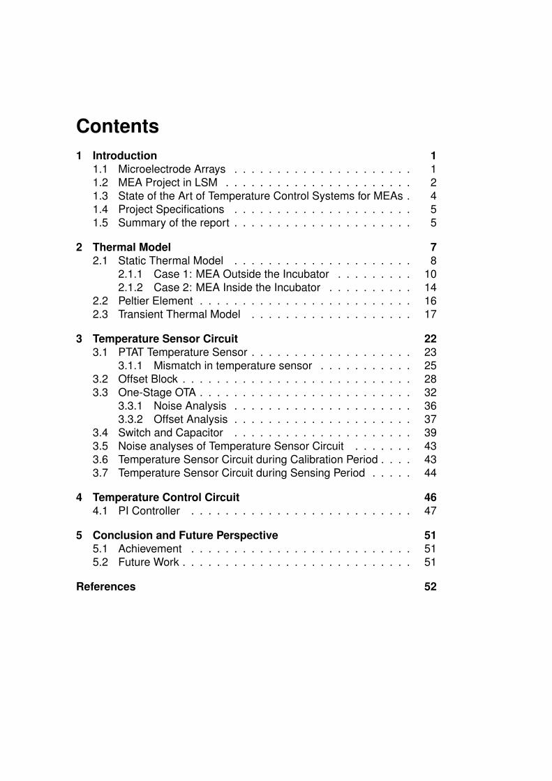
Contents1 Introduction 1
1.1 Microelectrode Arrays . . . . . . . . . . . . . . . . . . . . . 11.2 MEA Project in LSM . . . . . . . . . . . . . . . . . . . . . . 21.3 State of the Art of Temperature Control Systems for MEAs . 41.4 Project Specifications . . . . . . . . . . . . . . . . . . . . . 51.5 Summary of the report . . . . . . . . . . . . . . . . . . . . . 5
2 Thermal Model 72.1 Static Thermal Model . . . . . . . . . . . . . . . . . . . . . 8
2.1.1 Case 1: MEA Outside the Incubator . . . . . . . . . 102.1.2 Case 2: MEA Inside the Incubator . . . . . . . . . . 14
2.2 Peltier Element . . . . . . . . . . . . . . . . . . . . . . . . . 162.3 Transient Thermal Model . . . . . . . . . . . . . . . . . . . 17
3 Temperature Sensor Circuit 223.1 PTAT Temperature Sensor . . . . . . . . . . . . . . . . . . . 23
3.1.1 Mismatch in temperature sensor . . . . . . . . . . . 253.2 Offset Block . . . . . . . . . . . . . . . . . . . . . . . . . . . 283.3 One-Stage OTA . . . . . . . . . . . . . . . . . . . . . . . . . 32
3.3.1 Noise Analysis . . . . . . . . . . . . . . . . . . . . . 363.3.2 Offset Analysis . . . . . . . . . . . . . . . . . . . . . 37
3.4 Switch and Capacitor . . . . . . . . . . . . . . . . . . . . . 393.5 Noise analyses of Temperature Sensor Circuit . . . . . . . 433.6 Temperature Sensor Circuit during Calibration Period . . . . 433.7 Temperature Sensor Circuit during Sensing Period . . . . . 44
4 Temperature Control Circuit 464.1 PI Controller . . . . . . . . . . . . . . . . . . . . . . . . . . 47
5 Conclusion and Future Perspective 515.1 Achievement . . . . . . . . . . . . . . . . . . . . . . . . . . 515.2 Future Work . . . . . . . . . . . . . . . . . . . . . . . . . . . 51
References 52


List of Figures1.1 Commercial MEA from Multi Channel System MCS GMbH. 11.2 SEM image of cell culture lying on a CMOS-based MEA. . . 21.3 (a) SEM image of three-dimensional tip electrodes and (b)
the packaged MEA. . . . . . . . . . . . . . . . . . . . . . . 31.4 Conceptual cross-section of a CMOS-based MEA. . . . . . 42.1 Conceptual cross-section of the MEA system. . . . . . . . . 72.2 Static thermal model of the MEA. . . . . . . . . . . . . . . . 92.3 Cell temperature Tcell (a) and heat flow Q (b) versus the am-
bient temperature. . . . . . . . . . . . . . . . . . . . . . . . 112.4 (a) Temperature Thpeltier of the hot side of the peltier ele-
ment versus the ambient temperature. (b) Heat flow ver-sus the temperature difference between the two sides of thepeltier element. . . . . . . . . . . . . . . . . . . . . . . . . . 12
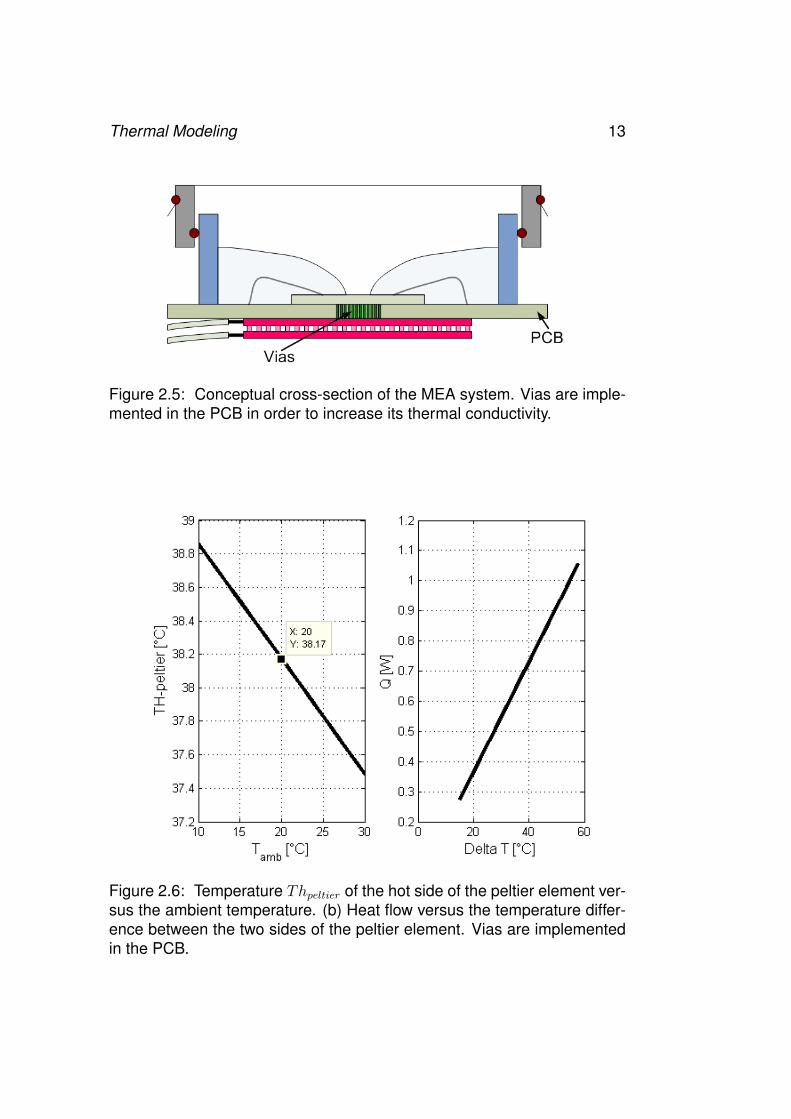
2.5 Conceptual cross-section of the MEA system. Vias are im-plemented in the PCB in order to increase its thermal con-ductivity. . . . . . . . . . . . . . . . . . . . . . . . . . . . . . 13
2.6 Temperature Thpeltier of the hot side of the peltier elementversus the ambient temperature. (b) Heat flow versus thetemperature difference between the two sides of the peltierelement. Vias are implemented in the PCB. . . . . . . . . . 13
2.7 Thermal model of the MEA during experimentation insidethe incubator. . . . . . . . . . . . . . . . . . . . . . . . . . . 14
2.8 Sensed temperature versus heat flow generated by theCMOS circuit for the case where the peltier element is notoperating. . . . . . . . . . . . . . . . . . . . . . . . . . . . . 15
2.9 Temperature of the upper side of the peltier element versusQCMOS. . . . . . . . . . . . . . . . . . . . . . . . . . . . . . 15
2.10 Performance curve of the peltier element CP1.4-71-10 (byMelcor). . . . . . . . . . . . . . . . . . . . . . . . . . . . . . 16
2.11 Transient thermal model of the MEA system. . . . . . . . . 182.12 Bode diagram of the transfer function Tsensor/Tamb. . . . . . 202.13 Bode diagram of the transfer function Tsensor/Thpeltier. . . . 213.1 Temperature sensor circuit schematic. . . . . . . . . . . . . 223.2 Temperature sensor topology. . . . . . . . . . . . . . . . . . 243.3 ∆VBE(T ) versus temperature for different current ratios.
The solid lines are simulated results under Cadence anddash lines are mathematical results. . . . . . . . . . . . . . 25
3.4 A model for bipolar mismatch calculation. . . . . . . . . . . 27
3.5 Circuit schematic of the offset block. . . . . . . . . . . . . . 293.6 (a) ∆Voff and ∆VBE versus temperature and (b) sensitivity
of the input and output signal of the Offset block. . . . . . . 313.7 Vctr versus temperature. . . . . . . . . . . . . . . . . . . . . 323.8 OTA circuit. . . . . . . . . . . . . . . . . . . . . . . . . . . . 333.9 gm versus inversion factor Ic. . . . . . . . . . . . . . . . . . 343.10 Noise in OTA. . . . . . . . . . . . . . . . . . . . . . . . . . . 363.11 Offset in OTA . . . . . . . . . . . . . . . . . . . . . . . . . . 383.12 Switch with capacitor. . . . . . . . . . . . . . . . . . . . . . 403.13 Vctr variation versus capacitor size. . . . . . . . . . . . . . . 413.14 (a) ∆Vctr versus time in capacitor leakage and (b) ∆Vctr Ver-
sus Temperature. . . . . . . . . . . . . . . . . . . . . . . . . 423.15 Temperature sensor circuit calibration. . . . . . . . . . . . . 443.16 Temperature sensor circuit sensing. . . . . . . . . . . . . . 454.1 Schematic of temperature control circuit with feedback. . . 464.2 (a)System response to unity step. (b) Noise response with
PI controller . . . . . . . . . . . . . . . . . . . . . . . . . . . 49


List of Tables2.1 Thermal model parameters. . . . . . . . . . . . . . . . . . . 102.2 Thermal resistance values. . . . . . . . . . . . . . . . . . . 102.3 Thermal model parameters. . . . . . . . . . . . . . . . . . . 172.4 Thermal capacitance values. . . . . . . . . . . . . . . . . . 183.1 Sensor sensitivity for different current ratios. The current I1
is set to 1µA. . . . . . . . . . . . . . . . . . . . . . . . . . . 243.2 CMOS transistor sizes of the PTAT temperature sensor. . . 253.3 Transistor sizes of the Offset block. . . . . . . . . . . . . . . 303.4 Transistor sizes of the Offset block. . . . . . . . . . . . . . 353.5 OTA transconductance values. . . . . . . . . . . . . . . . . 353.6 OTA characteristics. . . . . . . . . . . . . . . . . . . . . . . 363.7 Nominal, minimum and maximum sizes of the OTA’s transistor. 383.8 Parameters for calculating the offset of the OTA. . . . . . . 393.9 Switch parameters. . . . . . . . . . . . . . . . . . . . . . . 413.10 Noise analyses temperature sensor circuit . . . . . . . . . . 434.1 PI specifications. . . . . . . . . . . . . . . . . . . . . . . . . 50


Introduction 1
1 Introduction
1.1 Microelectrode ArraysMicroelectrode Arrays (MEAs) have become an essential tool both in fun-damental and applied electrophysiology research. They enable to stepfrom the observation of the electrical behaviour of single neurons towardsthe simultaneous analysis of population of neural cells [1]. Therefore, cellcultures on MEAs are well suited for the following applications:
• Drug development through screening of pharmacological effects ofcompounds [2].
• Understanding the brain operation by studying the electrical be-haviour of cell cultures. For example, learning [1] and epilepsy [3]can be investigated using cell cultures on MEAs.
• Building hybrid systems containing neurons and electronics [4]. Thesystem takes advantage of the learning capability of the cell cultureand the computation power of the electronic circuitry.
Commercial MEAs, as depicted in Figure (1.1), usually contain approx-imately 60 electrodes, with electrode sizes ranging from 10µm to 50µm,and inter-electrode spacing ranging up to 100µm [5]. These dimensionsare much larger than the 5− 20µm typical size of vertebrate neurons usedduring electrophysiological experiments [6]. Therefore, commercial MEAssuffer from a very low spatial resolution.
Figure 1.1: Commercial MEA from Multi Channel System MCS GMbH.
However recently, a new generation of silicon-based MEAs containing ahigh density and a large number (in the order of several thousands) of
2
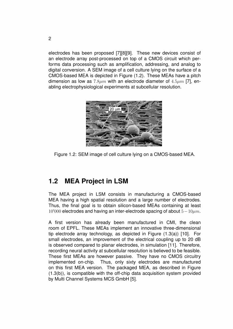
electrodes has been proposed [7][8][9]. These new devices consist ofan electrode array post-processed on top of a CMOS circuit which per-forms data processing such as amplification, addressing, and analog todigital conversion. A SEM image of a cell culture lying on the surface of aCMOS-based MEA is depicted in Figure (1.2). These MEAs have a pitchdimension as low as 7.8µm with an electrode diameter of 4.5µm [7], en-abling electrophysiological experiments at subcellular resolution.
Figure 1.2: SEM image of cell culture lying on a CMOS-based MEA.
1.2 MEA Project in LSM
The MEA project in LSM consists in manufacturing a CMOS-basedMEA having a high spatial resolution and a large number of electrodes.Thus, the final goal is to obtain silicon-based MEAs containing at least10′000 electrodes and having an inter-electrode spacing of about 5−10µm.
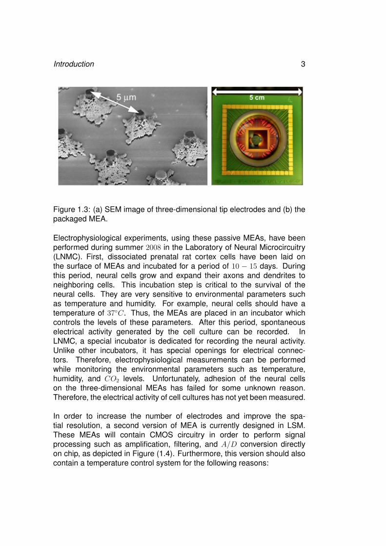
A first version has already been manufactured in CMI, the cleanroom of EPFL. These MEAs implement an innovative three-dimensionaltip electrode array technology, as depicted in Figure (1.3(a)) [10]. Forsmall electrodes, an improvement of the electrical coupling up to 20 dBis observed compared to planar electrodes, in simulation [11]. Therefore,recording neural activity at subcellular resolution is believed to be feasible.These first MEAs are however passive. They have no CMOS circuitryimplemented on-chip. Thus, only sixty electrodes are manufacturedon this first MEA version. The packaged MEA, as described in Figure(1.3(b)), is compatible with the off-chip data acquisition system providedby Multi Channel Systems MCS GmbH [5].
Introduction 3
Figure 1.3: (a) SEM image of three-dimensional tip electrodes and (b) thepackaged MEA.
Electrophysiological experiments, using these passive MEAs, have beenperformed during summer 2008 in the Laboratory of Neural Microcircuitry(LNMC). First, dissociated prenatal rat cortex cells have been laid onthe surface of MEAs and incubated for a period of 10 − 15 days. Duringthis period, neural cells grow and expand their axons and dendrites toneighboring cells. This incubation step is critical to the survival of theneural cells. They are very sensitive to environmental parameters suchas temperature and humidity. For example, neural cells should have atemperature of 37◦C. Thus, the MEAs are placed in an incubator whichcontrols the levels of these parameters. After this period, spontaneouselectrical activity generated by the cell culture can be recorded. InLNMC, a special incubator is dedicated for recording the neural activity.Unlike other incubators, it has special openings for electrical connec-tors. Therefore, electrophysiological measurements can be performedwhile monitoring the environmental parameters such as temperature,humidity, and CO2 levels. Unfortunately, adhesion of the neural cellson the three-dimensional MEAs has failed for some unknown reason.Therefore, the electrical activity of cell cultures has not yet been measured.
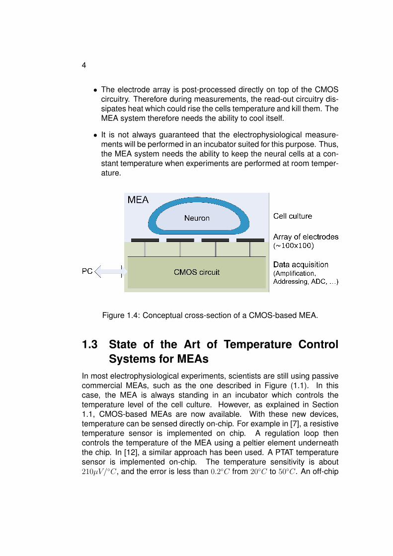
In order to increase the number of electrodes and improve the spa-tial resolution, a second version of MEA is currently designed in LSM.These MEAs will contain CMOS circuitry in order to perform signalprocessing such as amplification, filtering, and A/D conversion directlyon chip, as depicted in Figure (1.4). Furthermore, this version should alsocontain a temperature control system for the following reasons:
4
• The electrode array is post-processed directly on top of the CMOScircuitry. Therefore during measurements, the read-out circuitry dis-sipates heat which could rise the cells temperature and kill them. TheMEA system therefore needs the ability to cool itself.
• It is not always guaranteed that the electrophysiological measure-ments will be performed in an incubator suited for this purpose. Thus,the MEA system needs the ability to keep the neural cells at a con-stant temperature when experiments are performed at room temper-ature.
Figure 1.4: Conceptual cross-section of a CMOS-based MEA.
1.3 State of the Art of Temperature ControlSystems for MEAs
In most electrophysiological experiments, scientists are still using passivecommercial MEAs, such as the one described in Figure (1.1). In thiscase, the MEA is always standing in an incubator which controls thetemperature level of the cell culture. However, as explained in Section1.1, CMOS-based MEAs are now available. With these new devices,temperature can be sensed directly on-chip. For example in [7], a resistivetemperature sensor is implemented on chip. A regulation loop thencontrols the temperature of the MEA using a peltier element underneaththe chip. In [12], a similar approach has been used. A PTAT temperaturesensor is implemented on-chip. The temperature sensitivity is about210µV/◦C, and the error is less than 0.2◦C from 20◦C to 50◦C. An off-chip
Introduction 5
heating resistor then controls the MEAs temperature. Cooling is notnecessary since the on-chip electronics is low power. In [9], they claimto have used a heating element during electrophysiological experiments.However, no further details are given on the temperature sensor.
Finally, the two most sophisticated systems to our knowledge havebeen developed by the group of Prof. Kovacs in Stanford University [13],and by the group of Prof. Andreou in John Hopkins University [14]. Thesetwo groups attempt to integrate the cell culture with ”self incubation” inambient environment. Both have implemented a proportional-derivative-integral (PID) algorithm in order to control a heater.
1.4 Project SpecificationsThe goal of the project is to design a temperature control system whichkeeps the temperature of the cell culture at 37◦C ± 0.5◦C during biologicalmeasurements [13]. In between experiments, the MEA will stand in anincubator. However, during electrophysiological experiments, the temper-ature can either increase due to the heating of the CMOS circuitry, ordecrease due to the fact that the MEA has to be taken out of its incubatorfor electrical measurements. Thus, the temperature control system needsthe ability to heat and cool the MEA. For this reason, a peltier element isused instead of a heating resistor.
The on-chip temperature sensor has to be designed in UMC 0.18µmCMOS technology. If the temperature control system works correctly, itdoes not need to measure accurately the temperature outside the rangeof 35 − 40◦C. Moreover, the temperature sensor must have a negligibleeffect on the temperature of the MEA. Thus, its power consumption mustbe relatively low. Finally, the area occupied by the temperature sensormust not be too large, so an area smaller than 2′000µm2 is targeted.
1.5 Summary of the reportFirst, the thermal characteristics of the CMOS-based MEA are examined inChapter 2. The goal of this step is to define the specifications of the peltierelement and also to show that the temperature control system is capableof maintaining the cells at a constant temperature during experimentation.The temperature sensor circuit design is then described in Chapter 3, and

6
the temperature control system development is explained in Chapter 4.Finally, conclusion and future perspectives are discussed in Chapter 5.
Thermal Modeling 7
2 Thermal ModelBefore designing the on-chip temperature sensor and the temperaturecontrol circuit, it is necessary to analyze the heat transfer through thesystem. This step is needed in order to first prove the ability of thesystem to monitor the cell-culture temperature in real-time, and secondcharacterize the specification of the peltier element.
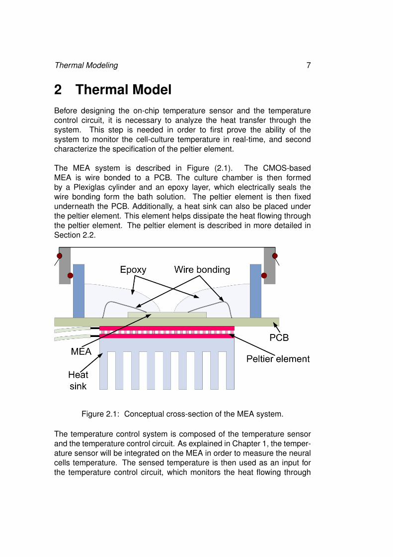
The MEA system is described in Figure (2.1). The CMOS-basedMEA is wire bonded to a PCB. The culture chamber is then formedby a Plexiglas cylinder and an epoxy layer, which electrically seals thewire bonding form the bath solution. The peltier element is then fixedunderneath the PCB. Additionally, a heat sink can also be placed underthe peltier element. This element helps dissipate the heat flowing throughthe peltier element. The peltier element is described in more detailed inSection 2.2.
Figure 2.1: Conceptual cross-section of the MEA system.
The temperature control system is composed of the temperature sensorand the temperature control circuit. As explained in Chapter 1, the temper-ature sensor will be integrated on the MEA in order to measure the neuralcells temperature. The sensed temperature is then used as an input forthe temperature control circuit, which monitors the heat flowing through
8
the peletier element. As a first step, the temperature control circuit willbe implemented on the PCB with discrete elements. Future version of thesystem might integrate the temperature control circuit on the CMOS-basedMEA.
2.1 Static Thermal ModelThe static thermal model of the MEA system is depicted in Figure (2.2).It is described by the thermal resistance Θ[K/W ] of each material con-stituting the MEA system (electrolyte, MEA, PCB,· · · ), the heat flow Q[W ]through each of these element, and the temperature T [◦C,K] at each pointof the system. In another word, the thermal circuit is equivalent to an elec-trical circuit where the thermal resistance Θ, the heat flow Q, and the tem-perature T are equivalent to the electrical resistance R[Ohm], the currentI[A], and the voltage V [V ]. Thus, the heat transfer equation is describedas:
Θ =∆T
Q=
t
kA(2.1)
where t[m] is the material thickness, k[W/mK] is the thermal conductivityof the material and A[m2] is the transfer area of the material.
The thermal model parameters are described in Table(2.1). The thermalconductivity values are taken from [15], [16], and [17]. Moreover, the fol-lowing hypotheses have been made:
• The material between the temperature sensor, which is at the tran-sistor level, and the surface of the MEA is composed of all the ma-terials necessary for the CMOS circuit wiring: Silicon dioxide (SiO2),Aluminium (Al), Tungsten (W ), and more. However, in the thermalmodel described in Figure (2.2), only SiO2 is considered because ithas the lowest thermal conductivity. This case has been chosen inorder to describe the maximum temperature difference between Tcelland Tsensor.
• The electrolyte solution is supposed to have the same thermal char-acteristics as water. Thus in this project, the electrolyte is consideredto be water.
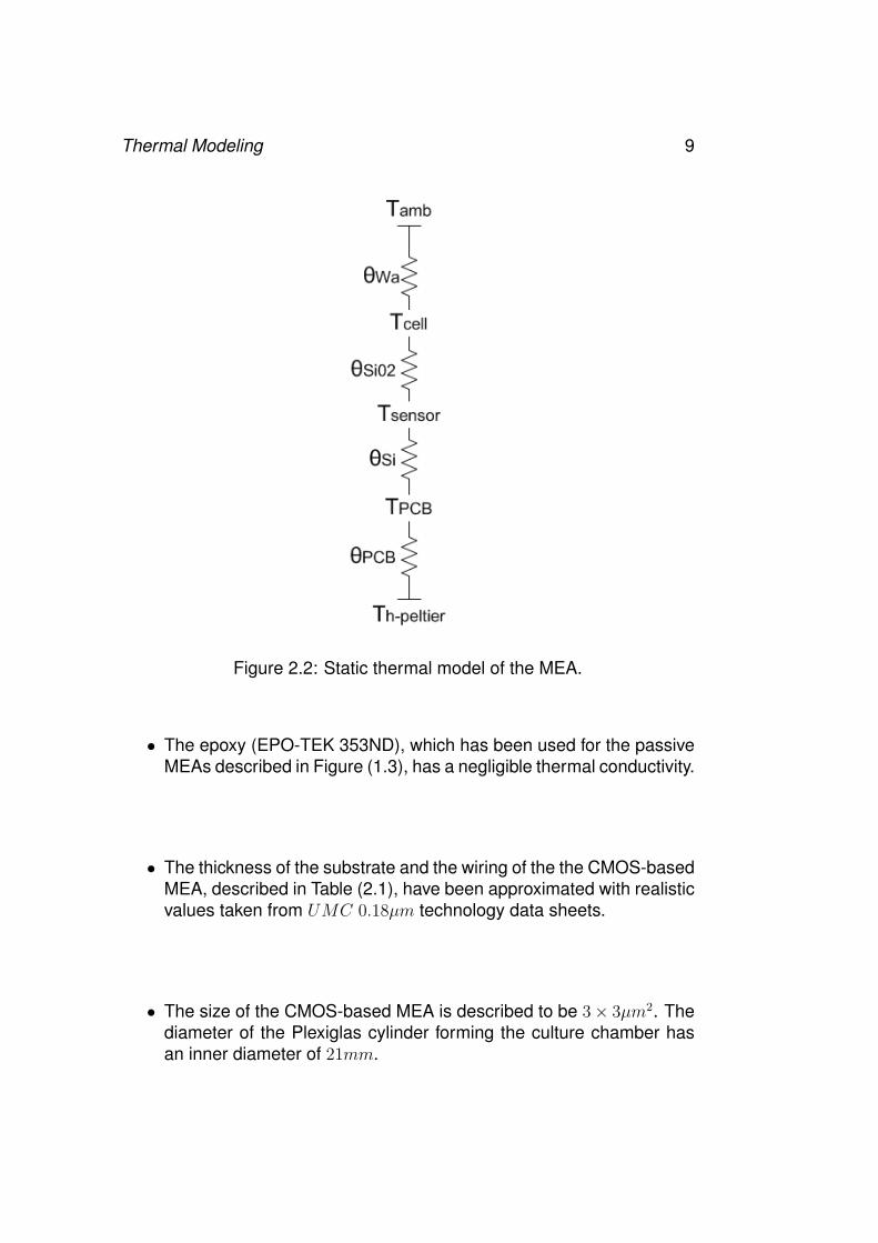
Thermal Modeling 9
Figure 2.2: Static thermal model of the MEA.
• The epoxy (EPO-TEK 353ND), which has been used for the passiveMEAs described in Figure (1.3), has a negligible thermal conductivity.
• The thickness of the substrate and the wiring of the the CMOS-basedMEA, described in Table (2.1), have been approximated with realisticvalues taken from UMC 0.18µm technology data sheets.
• The size of the CMOS-based MEA is described to be 3× 3µm2. Thediameter of the Plexiglas cylinder forming the culture chamber hasan inner diameter of 21mm.
10
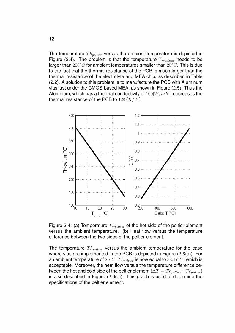
Material Type Material Thickness Thermal Conductivity Material Areat[m] k[W/mK] A[m2]
PCB 1.25e−3 0.4 9e−6
Si 500e−6 149 9e−6
SiO2 8e−6 1 9e−6
Water 0.005 0.585 3.46−4
Table 2.1: Thermal model parameters.
The thermal resistance values are given in Table (2.2). They have beencalculated with Equation (2.1) and using the parameters given in Table(2.1).
Material Type Thermal resistorsΘ[K/W ]
PCB 347(Si) 0.373SiO2 0.889Water 24.7
Table 2.2: Thermal resistance values.
2.1.1 Case 1: MEA Outside the Incubator
When the MEA is taken out of its incubator, the ambient temperaturedrops from 37◦C to room temperature (by default 20◦C). Thus, a heatflow through the electrolyte and SiO2 is created and can be described inEquation (2.2). In order to keep the sensor temperature Tsensor constant,the same amount of heat must be injected by the peltier element throughthe PCB and the substrate Si. Knowing the heat flow, the temperature atthe surface of the MEA Tcell can then be calculated using Equation (2.3).
Q = (Tsensor − Tamb)/(Θwa + ΘSiO2) (2.2)
Tcell = Tsensor − (QΘSiO2) (2.3)
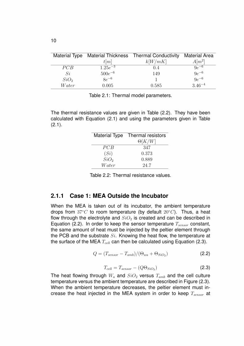
The heat flowing through Wa and SiO2 versus Tamb and the cell culturetemperature versus the ambient temperature are described in Figure (2.3).When the ambient temperature decreases, the peltier element must in-crease the heat injected in the MEA system in order to keep Tsensor at
Thermal Modeling 11
37◦C. For a typical ambient temperature between 20− 25◦C, the heat flowis equal to 0.7 ± 0.1W . It is also interesting to notice that the temperatureTsensor which is sensed is not exactly equal to the cell culture temperature.For example, at an ambient temperature of 20◦C, Tcell is equal to 36.41◦Cwhile the sensor is sensing 37◦C. Thus, the temperature control systemshould maintain Tsensor at the value of 37.5◦C in order to have the culturecell around 37± 0.5◦C.
Figure 2.3: Cell temperature Tcell (a) and heat flow Q (b) versus the ambi-ent temperature.
As explained in previous paragraphs, the peltier element must inject thesame amount of heat as the heat flowing out of the MEA in order to keepTsensor at a constant value. Thus Thpeltier, which is the temperature on thehotter side of the peltier element, can be calculated using Equation (2.4).The temperature difference between the hot and cold side of the peltierelement can also be expressed as in Equation (2.5).
Thpeltier = (Θsi + ΘPCB)Q+ Tsensor (2.4)
∆T = 2(Thpeltier − Tamb) (2.5)
12
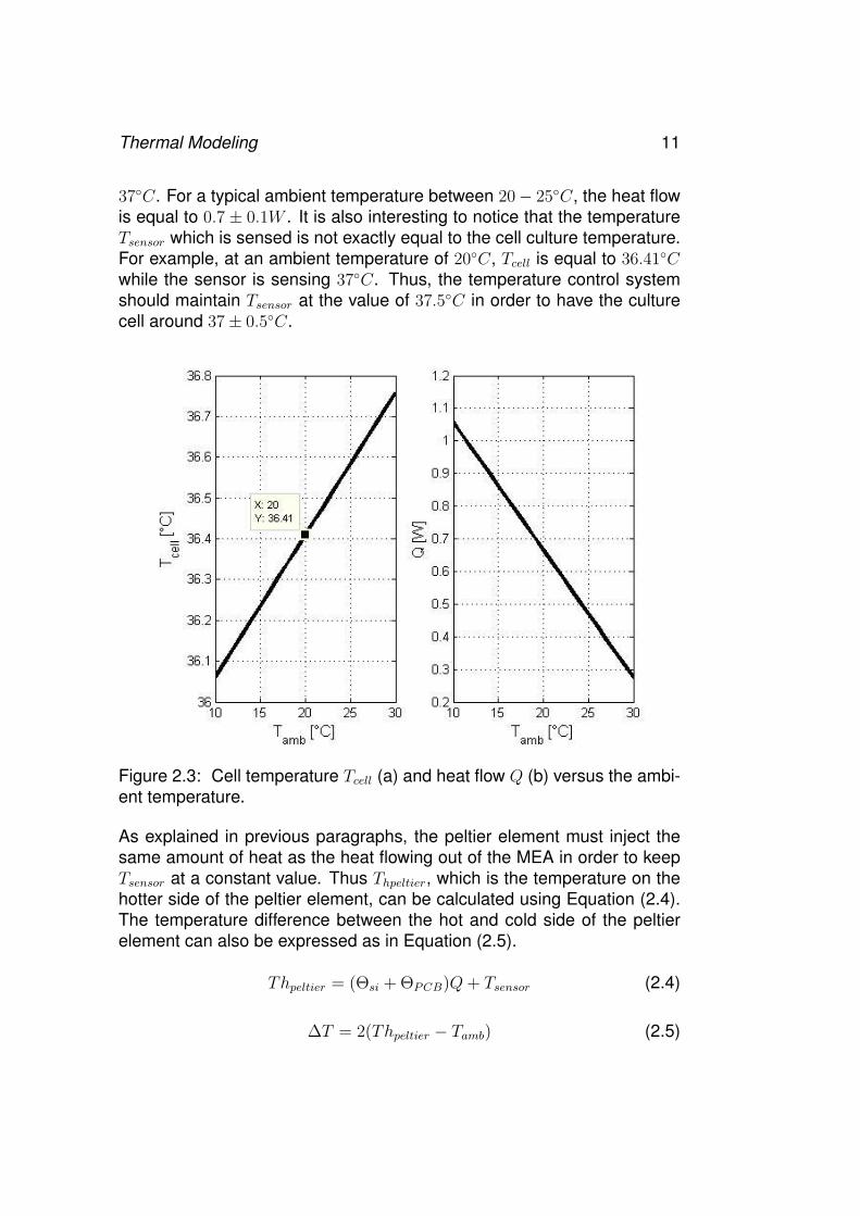
The temperature Thpeltier versus the ambient temperature is depicted inFigure (2.4). The problem is that the temperature Thpeltier needs to belarger than 200◦C for ambient temperatures smaller than 25◦C. This is dueto the fact that the thermal resistance of the PCB is much larger than thethermal resistance of the electrolyte and MEA chip, as described in Table(2.2). A solution to this problem is to manufacture the PCB with Aluminumvias just under the CMOS-based MEA, as shown in Figure (2.5). Thus theAluminum, which has a thermal conductivity of 100[W/mK], decreases thethermal resistance of the PCB to 1.39[K/W ].
Figure 2.4: (a) Temperature Thpeltier of the hot side of the peltier elementversus the ambient temperature. (b) Heat flow versus the temperaturedifference between the two sides of the peltier element.
The temperature Thpeltier versus the ambient temperature for the casewhere vias are implemented in the PCB is depicted in Figure (2.6(a)). Foran ambient temperature of 20◦C, Thpeltier is now equal to 38.17◦C, which isacceptable. Moreover, the heat flow versus the temperature difference be-tween the hot and cold side of the peltier element (∆T = Thpeltier−Tcpeltier)is also described in Figure (2.6(b)). This graph is used to determine thespecifications of the peltier element.
Thermal Modeling 13
Figure 2.5: Conceptual cross-section of the MEA system. Vias are imple-mented in the PCB in order to increase its thermal conductivity.
Figure 2.6: Temperature Thpeltier of the hot side of the peltier element ver-sus the ambient temperature. (b) Heat flow versus the temperature differ-ence between the two sides of the peltier element. Vias are implementedin the PCB.
14
2.1.2 Case 2: MEA Inside the Incubator
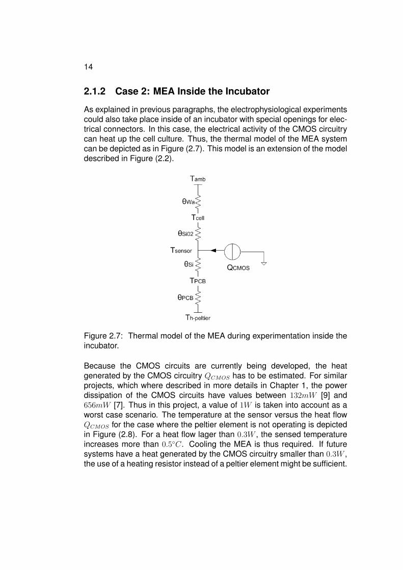
As explained in previous paragraphs, the electrophysiological experimentscould also take place inside of an incubator with special openings for elec-trical connectors. In this case, the electrical activity of the CMOS circuitrycan heat up the cell culture. Thus, the thermal model of the MEA systemcan be depicted as in Figure (2.7). This model is an extension of the modeldescribed in Figure (2.2).
Figure 2.7: Thermal model of the MEA during experimentation inside theincubator.
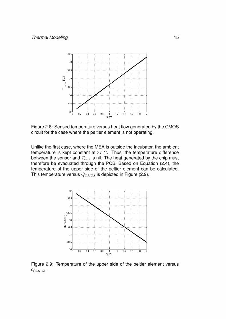
Because the CMOS circuits are currently being developed, the heatgenerated by the CMOS circuitry QCMOS has to be estimated. For similarprojects, which where described in more details in Chapter 1, the powerdissipation of the CMOS circuits have values between 132mW [9] and656mW [7]. Thus in this project, a value of 1W is taken into account as aworst case scenario. The temperature at the sensor versus the heat flowQCMOS for the case where the peltier element is not operating is depictedin Figure (2.8). For a heat flow lager than 0.3W , the sensed temperatureincreases more than 0.5◦C. Cooling the MEA is thus required. If futuresystems have a heat generated by the CMOS circuitry smaller than 0.3W ,the use of a heating resistor instead of a peltier element might be sufficient.
Thermal Modeling 15
Figure 2.8: Sensed temperature versus heat flow generated by the CMOScircuit for the case where the peltier element is not operating.
Unlike the first case, where the MEA is outside the incubator, the ambienttemperature is kept constant at 37◦C. Thus, the temperature differencebetween the sensor and Tamb is nil. The heat generated by the chip musttherefore be evacuated through the PCB. Based on Equation (2.4), thetemperature of the upper side of the peltier element can be calculated.This temperature versus QCMOS is depicted in Figure (2.9).
Figure 2.9: Temperature of the upper side of the peltier element versusQCMOS.
16
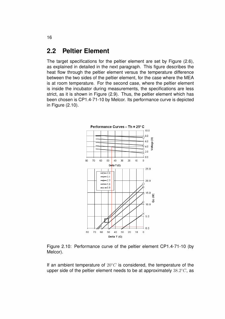
2.2 Peltier ElementThe target specifications for the peltier element are set by Figure (2.6),as explained in detailed in the next paragraph. This figure describes theheat flow through the peltier element versus the temperature differencebetween the two sides of the peltier element, for the case where the MEAis at room temperature. For the second case, where the peltier elementis inside the incubator during measurements, the specifications are lessstrict, as it is shown in Figure (2.9). Thus, the peltier element which hasbeen chosen is CP1.4-71-10 by Melcor. Its performance curve is depictedin Figure (2.10).
Figure 2.10: Performance curve of the peltier element CP1.4-71-10 (byMelcor).
If an ambient temperature of 20◦C is considered, the temperature of theupper side of the peltier element needs to be at approximately 38.2◦C, as

Thermal Modeling 17
described in Figure (2.6). The difference between the two sides of thepeltier element is thus equal to 36.4◦C, as calculated by Equation (2.5).Moreover, as shown in Figure (2.6), the heat flow is approximately equal to0.6W at a room temperature of 20◦C. The equation describing the peltierelement, which will be used in Chapter 4, can now be found using theperformance curves of the peltier element. In order to have a securitymargin, the point (T,Q) = (49, 0.6) is considered. The input current of thepeltier element is thus equal to 1.6A, as described in Figure (2.10). Theequation describing the peltier element is thus described as:
Vpeltier = 1.66e−2∆T + 3 = 1.66e−2Thpeltier − 1.66e−2Tcpeltier + 3 (2.6)
2.3 Transient Thermal ModelIn section 2.1, a static flow model is developed. However, transient heatflow should be considered for designing the temperature control circuit.Transient heat transfer depends on thermal capacitance of the system,which is calculated as follows:
CΘ = ρcρV (2.7)
where CΘ [J/K] is the thermal capacitance, ρ [g/m3] is the density of themedium, cρ [J/gK] is the specific heat of the medium, and V [m3] is thevolume of the material.Table (2.3) shows the values of the medium density,specific heat, and volume for each material used in the system.
Material Type Medium Density Medium Specific Heat Volumeρ[g/m3] cρ[J/gk] V [m3]
PCB 1.91e06 0.6 3.125e−06
Silicon (Si) 2.33e06 0.71 4.5e−09
Silicon Dioxide 10e06 1 72e−012
(SiO2)Water 1e06 4.18 1.73e−06
Table 2.3: Thermal model parameters.
Using the values of Table (2.3), the thermal capacitance of materials arecalculated and described in Table (2.4).
18
Material Type thermal capacitanceCΘ [J/K]
PCB 3.58Silicon (Si) 7.46e−03
Silicon Dioxide 0.72e−03
(SiO2)Water 7.29
Table 2.4: Thermal capacitance values.
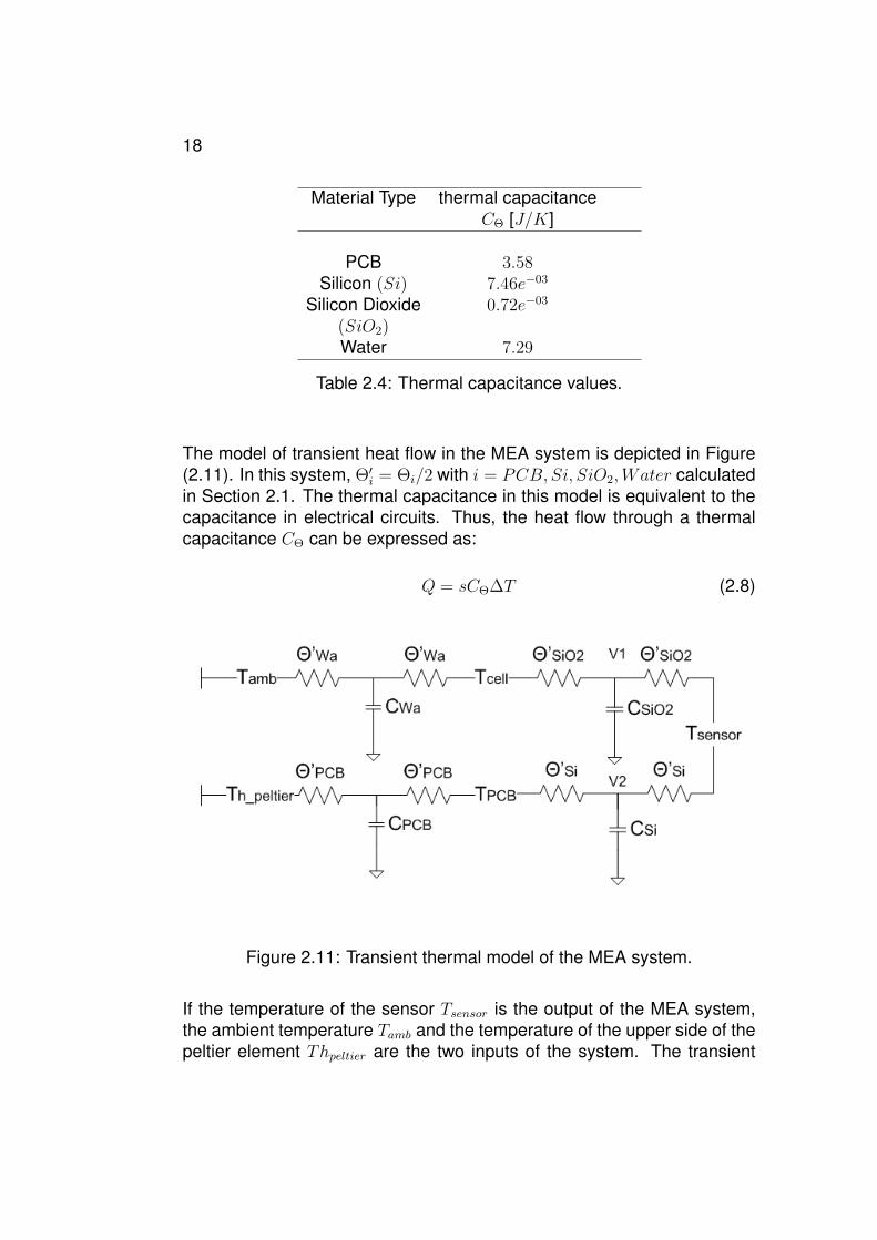
The model of transient heat flow in the MEA system is depicted in Figure(2.11). In this system, Θ′i = Θi/2 with i = PCB, Si, SiO2,Water calculatedin Section 2.1. The thermal capacitance in this model is equivalent to thecapacitance in electrical circuits. Thus, the heat flow through a thermalcapacitance CΘ can be expressed as:
Q = sCΘ∆T (2.8)
Figure 2.11: Transient thermal model of the MEA system.
If the temperature of the sensor Tsensor is the output of the MEA system,the ambient temperature Tamb and the temperature of the upper side of thepeltier element Thpeltier are the two inputs of the system. The transient
Thermal Modeling 19
heat flow of the system is expressed as:
Tsensor =Θ′Si
Θ′Si + Θ′SiO2
V1 +Θ′SiO2
Θ′Si02+ Θ′Si
V2 (2.9)
The thermal circuit from Tamb to V1 and Thpeltier to V2 is equivalent to a sec-ond order low pass filter. Thus, V1 and V2 can be described by Equations(2.10) and (2.11).
V1 =B
s2 + As+BTamb (2.10)
A = C−1Si02
(Θ′Wa + Θ′SiO2)−1 + C−1
WaΘ′−1Wa + C−1
Wa(Θ′Wa + Θ′SiO2
)−1
B = C−1WaC
−1SiO2
Θ′−1Wa(Θ
′Wa + Θ′SiO2
)−1
and:V2 =
D
s2 + Cs+DThpeltier (2.11)
C = C−1Si (Θ′PCB + Θ′Si)
−1 + C−1PCBΘ′−1
PCB + C−1PCB(Θ′PCB + Θ′Si)
−1
D = C−1PCBC
−1Si Θ′−1
PCB(Θ′PCB + Θ′Si)−1
Finally, Tsensor can be expressed as follows:
Tsensor =Θ′Si
(Θ′SiO2+ Θ′Si)
B
s2 + Ap+BTamb+
Θ′SiO2
(Θ′SiO2+ Θ′Si)
D
s2 + Cs+DThpeltier
(2.12)
A = C−1Si02
(Θ′Wa + Θ′SiO2)−1 + C−1
WaΘ′−1Wa + C−1
Wa(Θ′Wa + Θ′SiO2
)−1
B = C−1WaC
−1SiO2
Θ′−1Wa(Θ
′Wa + Θ′SiO2
)−1
C = C−1Si (Θ′PCB + Θ′Si)
−1 + C−1PCBΘ′−1
PCB + C−1PCB(Θ′PCB + Θ′Si)
−1
D = C−1PCBC
−1Si Θ′−1
PCB(Θ′PCB + Θ′Si)−1
The numerical solution of Equation (2.12) is described in the followingequation:
Tsensor =0.35943
s2 + 108.7s+ 1.216Tamb +
43.12
s2 + 152.9s+ 61.21Thpeltier (2.13)
20
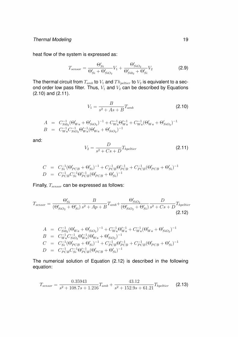
Figure 2.12: Bode diagram of the transfer function Tsensor/Tamb.
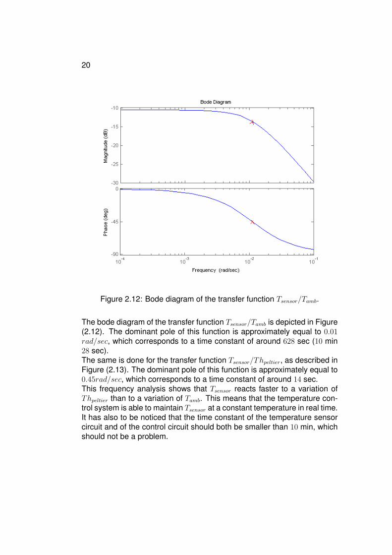
The bode diagram of the transfer function Tsensor/Tamb is depicted in Figure(2.12). The dominant pole of this function is approximately equal to 0.01rad/sec, which corresponds to a time constant of around 628 sec (10 min28 sec).The same is done for the transfer function Tsensor/Thpeltier, as described inFigure (2.13). The dominant pole of this function is approximately equal to0.45rad/sec, which corresponds to a time constant of around 14 sec.This frequency analysis shows that Tsensor reacts faster to a variation ofThpeltier than to a variation of Tamb. This means that the temperature con-trol system is able to maintain Tsensor at a constant temperature in real time.It has also to be noticed that the time constant of the temperature sensorcircuit and of the control circuit should both be smaller than 10 min, whichshould not be a problem.
Thermal Modeling 21
Figure 2.13: Bode diagram of the transfer function Tsensor/Thpeltier.
22
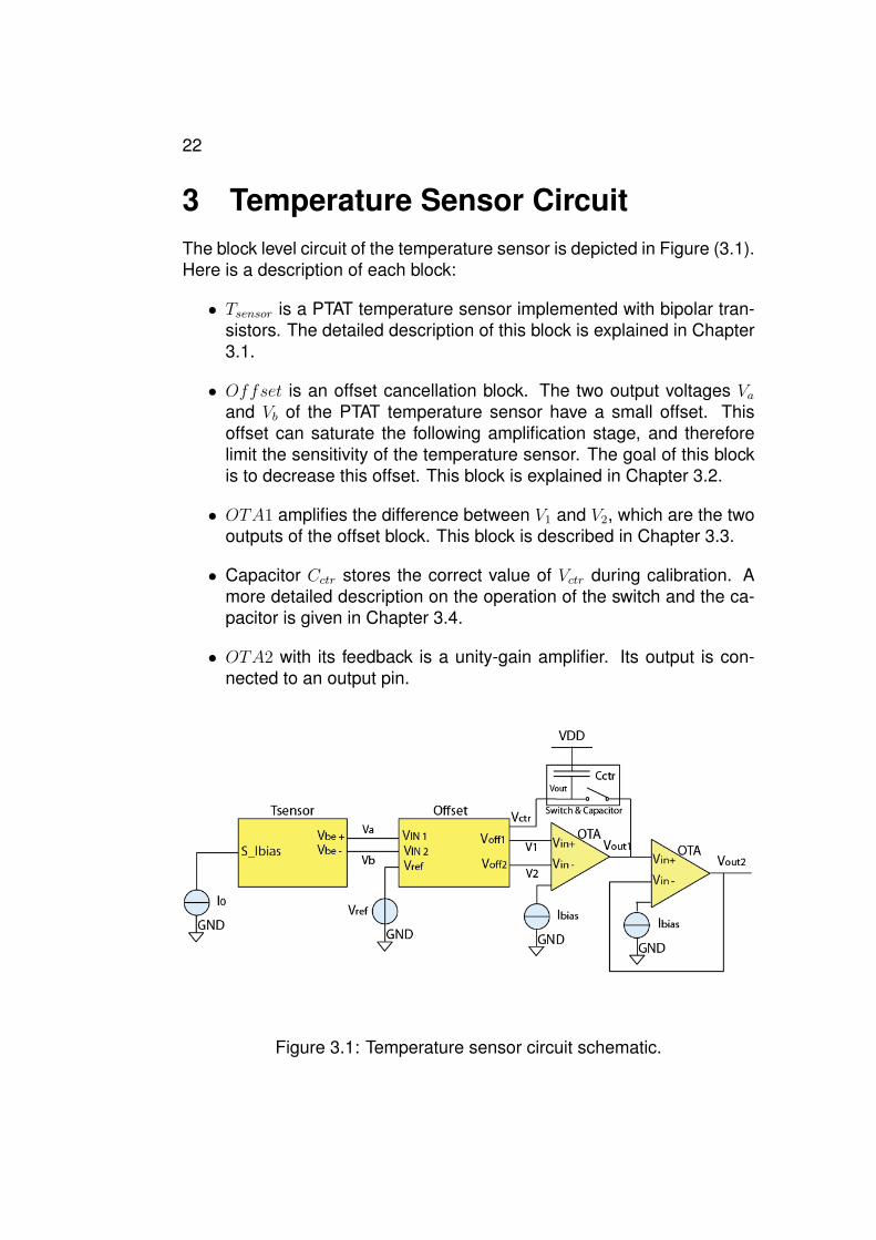
3 Temperature Sensor CircuitThe block level circuit of the temperature sensor is depicted in Figure (3.1).Here is a description of each block:
• Tsensor is a PTAT temperature sensor implemented with bipolar tran-sistors. The detailed description of this block is explained in Chapter3.1.
• Offset is an offset cancellation block. The two output voltages Vaand Vb of the PTAT temperature sensor have a small offset. Thisoffset can saturate the following amplification stage, and thereforelimit the sensitivity of the temperature sensor. The goal of this blockis to decrease this offset. This block is explained in Chapter 3.2.
• OTA1 amplifies the difference between V1 and V2, which are the twooutputs of the offset block. This block is described in Chapter 3.3.
• Capacitor Cctr stores the correct value of Vctr during calibration. Amore detailed description on the operation of the switch and the ca-pacitor is given in Chapter 3.4.
• OTA2 with its feedback is a unity-gain amplifier. Its output is con-nected to an output pin.
Figure 3.1: Temperature sensor circuit schematic.
Temperature Sensor Circuit 23
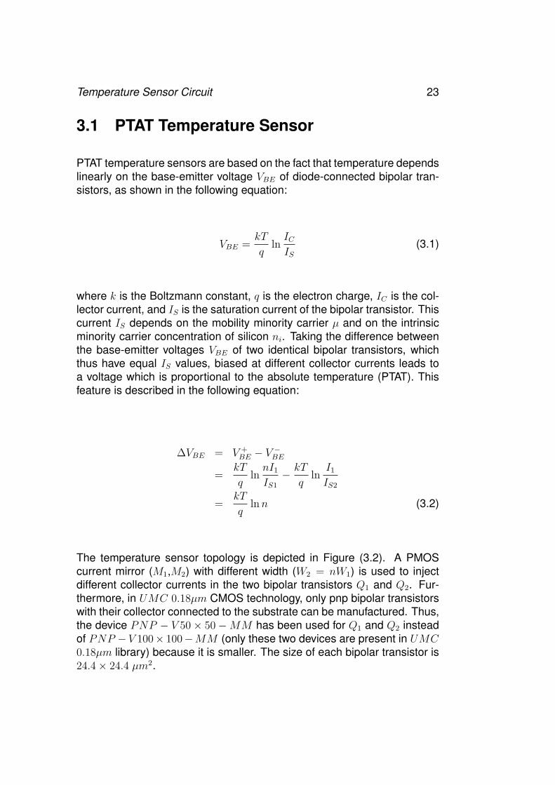
3.1 PTAT Temperature Sensor
PTAT temperature sensors are based on the fact that temperature dependslinearly on the base-emitter voltage VBE of diode-connected bipolar tran-sistors, as shown in the following equation:
VBE =kT
qlnICIS
(3.1)
where k is the Boltzmann constant, q is the electron charge, IC is the col-lector current, and IS is the saturation current of the bipolar transistor. Thiscurrent IS depends on the mobility minority carrier µ and on the intrinsicminority carrier concentration of silicon ni. Taking the difference betweenthe base-emitter voltages VBE of two identical bipolar transistors, whichthus have equal IS values, biased at different collector currents leads toa voltage which is proportional to the absolute temperature (PTAT). Thisfeature is described in the following equation:
∆VBE = V +BE − V
−BE
=kT
qlnnI1
IS1
− kT
qln
I1
IS2
=kT
qlnn (3.2)
The temperature sensor topology is depicted in Figure (3.2). A PMOScurrent mirror (M1,M2) with different width (W2 = nW1) is used to injectdifferent collector currents in the two bipolar transistors Q1 and Q2. Fur-thermore, in UMC 0.18µm CMOS technology, only pnp bipolar transistorswith their collector connected to the substrate can be manufactured. Thus,the device PNP − V 50× 50−MM has been used for Q1 and Q2 insteadof PNP − V 100× 100−MM (only these two devices are present in UMC0.18µm library) because it is smaller. The size of each bipolar transistor is24.4× 24.4 µm2.
24
Figure 3.2: Temperature sensor topology.
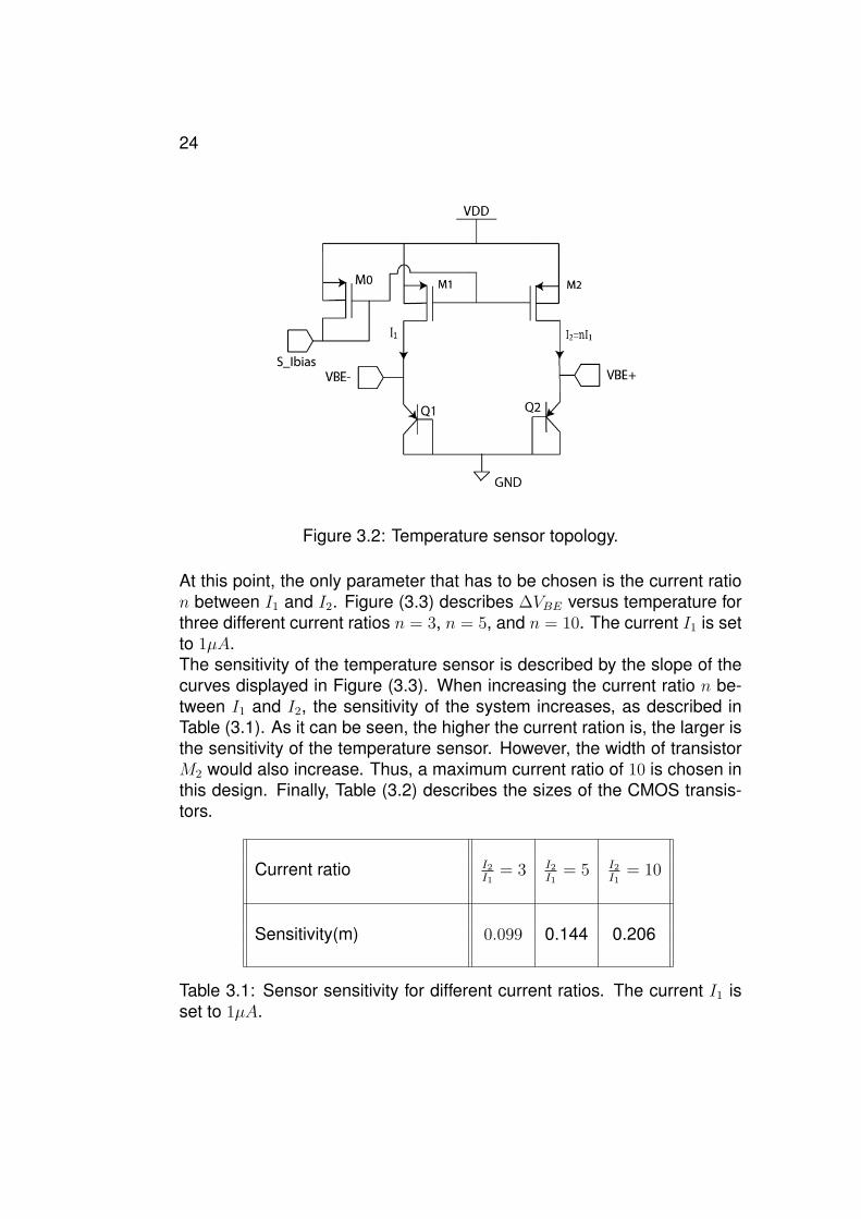
At this point, the only parameter that has to be chosen is the current ration between I1 and I2. Figure (3.3) describes ∆VBE versus temperature forthree different current ratios n = 3, n = 5, and n = 10. The current I1 is setto 1µA.The sensitivity of the temperature sensor is described by the slope of thecurves displayed in Figure (3.3). When increasing the current ratio n be-tween I1 and I2, the sensitivity of the system increases, as described inTable (3.1). As it can be seen, the higher the current ration is, the larger isthe sensitivity of the temperature sensor. However, the width of transistorM2 would also increase. Thus, a maximum current ratio of 10 is chosen inthis design. Finally, Table (3.2) describes the sizes of the CMOS transis-tors.
Current ratio I2I1
= 3 I2I1
= 5 I2I1
= 10
Sensitivity(m) 0.099 0.144 0.206
Table 3.1: Sensor sensitivity for different current ratios. The current I1 isset to 1µA.
Temperature Sensor Circuit 25
Figure 3.3: ∆VBE(T ) versus temperature for different current ratios. Thesolid lines are simulated results under Cadence and dash lines are math-ematical results.
PMOS I[µA] W [µm] L [µm]
M0,1 1 1 1M2 10 10 1
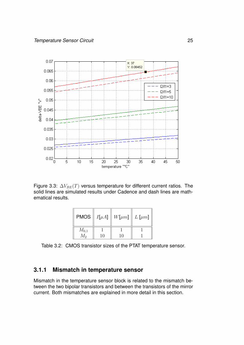
Table 3.2: CMOS transistor sizes of the PTAT temperature sensor.
3.1.1 Mismatch in temperature sensor
Mismatch in the temperature sensor block is related to the mismatch be-tween the two bipolar transistors and between the transistors of the mirrorcurrent. Both mismatches are explained in more detail in this section.
26
• Mismatch in current mirror
The mismatch between M1 and M2 can be expressed as inthe following equation:
σ
(δIDID
)=
√σ2B +
(gmIDσT
)2
(3.3)
Both transistors M1 and M2 operate in strong inversion. Thus, thevariance of (δID/ID) is mainly due to the mismatch of β. Moreover,with the transistors sizes given in Table (3.2), the mismatch can beapproximated from [18]. In this case, (δID/ID) = 5% is consideredhas a realistic worst case value. Since Monte Carlo simulationscould not be undertaken using UMC design kit, more precise valuesfor the mismatch will have to be experimentally measured.
Finally, it has to be notice that in order to limit the mismatch ofthe current mirror, M2 should be designed as ten transistors inparallel. Thus, all transistors would have the same size (width andlength equal to 1µm).
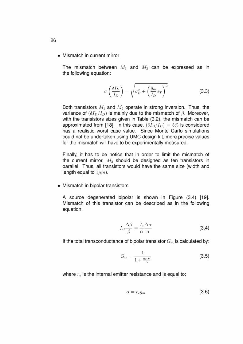
• Mismatch in bipolar transistors
A source degenerated bipolar is shown in Figure (3.4) [19].Mismatch of this transistor can be described as in the followingequation:
IB∆β
β=Icα
∆α
α(3.4)
If the total transconductance of bipolar transistor Gm is calculated by:
Gm =1
1 + gmRα
(3.5)
where re is the internal emitter resistance and is equal to:
α = regm (3.6)
Temperature Sensor Circuit 27
Figure 3.4: A model for bipolar mismatch calculation.
By combination of Equations (3.5), (3.6) and (3.4), the mismatch ofthe bipolar transistor in Figure (3.4) is obtained by:
∆IcIc
=
(1
1 + gmRα
)∆IsIs
+
(gmRα
1 + gmRα
)(∆α
α− ∆R
R
)(3.7)
According to Figure (3.2), R = 0 in this project. Thus, Equation (3.7)can be expressed as:
∆IcIc
=∆IsIs
(3.8)
This value can not be determined using UMC 0.18µm technologyreports. Current mismatch between the two bipolar transistors willtherefore have to be experimentally measured.
28
3.2 Offset Block
As shown in Equation (3.2), ∆VBE is used to sense the temperature of thesystem. Usually this value is amplified in order to increase the sensitivityof the sensor. However, as depicted in Figure (3.3), ∆VBE is approximatelyequal to 60mV when the temperature is 37◦C. If an amplification stagewith a gain of 40 dB is then used, the output of this stage would saturate.Thus, the goal of the offset block is to decrease the value of ∆VBE whilemaintaining approximately the same sensitivity (same slope of ∆VBE).This innovative idea has, to our knowledge, not being implemented in anyother temperature sensor.
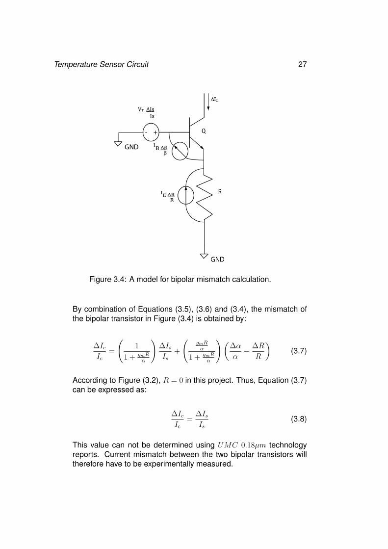
The circuit schematic of the offset block is depicted in Figure (3.5).The output signals of the PTAT temperature sensor are connected totwo identical NMOS transistors M1 and M2. The largest signal V +
BE isconnected to VIN2 and the smallest signal V −BE is connected to VIN1. Thethree PMOS transistors, M3, M4, and M5, have identical sizes. Thus, if nocurrent is flowing through M5, the two currents I3 and I4 are equal. Then,because the drain current of M1 and M2 and their sizes are identical, Voff2
will have a larger value than Voff1. This is due to the fact that V +BE is larger
than V −BE. The idea is thus increase the drain current of M2 in order toincrease Voff1. This is why a PMOS transistor M5 has been added inparallel with M4. How to set Vctr to the correct value is explained in afollowing paragraph.
The relationship between the input signal VBE and its output signals Voff1
and Voff2 has to be determined. The two input voltages VIN1 and VIN2,which are equal to the voltage at the emitter of the two bipolar transistors,have values around 600 − 700mV . Thus, transistors M1 and M2 operatein saturation. In order to better control the output voltages, transistors M3
and M4 should operate in the triode region. Therefore, Vref is fixed to 0V.Moreover, if all transistors have the same length, the width of transistorsM1 and M2 (W1,2) should be larger than W3,4.
The drain current of M1 and M2 can be expressed as:
I1,2 =β
2n
(VG1,2 − VT0
)2 (3.9)
Temperature Sensor Circuit 29
Moreover the current in the triode region is defined as:
Itriode = β(VD − VS)[VG − VT0 −
n
2(VD + VS)
](3.10)
where VD is the drain voltage and VS is the source voltage. As shown inFigure (3.5), I3 is equal to I1, thus the following equation can be made:
Figure 3.5: Circuit schematic of the offset block.
β1
2nn(VV IN2 − VT0n)2 = β3(VDD−Voff2)
[VDD − Vref − VT0p −
np2
(VDD + Voff2)]
(3.11)Vctr is equivalent to the output voltage of the amplification stage OTA, asdepicted in Figure (3.1). It can thus be expressed as:
Vctr = Av(Voff1 − Voff2) (3.12)
where Av is the gain of the OTA in open loop. Furthermore, I2 is equal tothe sum of I4 and I5, as depicted in Figure (3.5). Thus, for the case whereM5 operates in saturation, the following equation can be made:
30
β1
2nn(VV IN2 − VT0n)2 = β3(VDD − Voff2)
[VDD − Vref − VT0p −
np2
(VDD + Voff2)]
+β5
2np
(VDD − Vctr − VT0p
)2 (3.13)
The sizes of the transistors are given in Table (3.3). The transistors widthsare set in order to have M1,2 operating in saturation and M3,4,5 operatingin the triode region. If W1,2 is too large compared to W3,4,5, M3,4 operate inthe saturation region and not in the triode region. However, if W1,2 is toosmall compared to W3,4,5, the output voltages Voff1 and Voff2 saturate topower supply. Moreover, the length of the transistors is set to 15µm. Thisvalue is quite large in order to limit the current consumption of the block.With the transistor sizes given in Table (3.3), I1 is equal to 9.5µA and I2 isequal to 13.1µA.
PMOS W [µm] L [µm]
M1,2 10 15M3,4,5 4.5 15
Table 3.3: Transistor sizes of the Offset block.
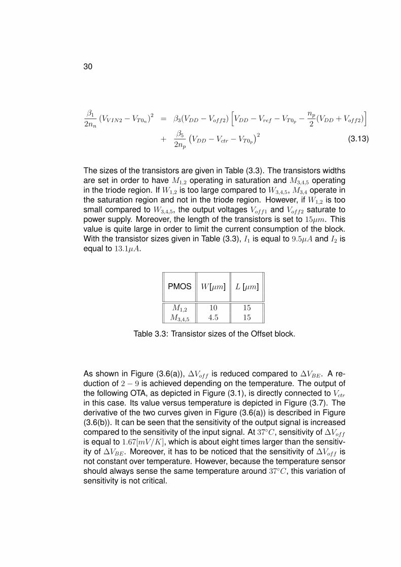
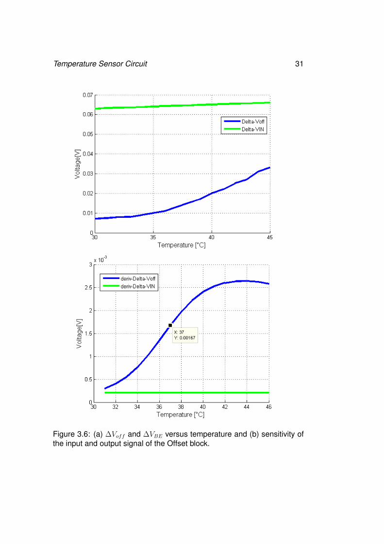
As shown in Figure (3.6(a)), ∆Voff is reduced compared to ∆VBE. A re-duction of 2 − 9 is achieved depending on the temperature. The output ofthe following OTA, as depicted in Figure (3.1), is directly connected to Vctrin this case. Its value versus temperature is depicted in Figure (3.7). Thederivative of the two curves given in Figure (3.6(a)) is described in Figure(3.6(b)). It can be seen that the sensitivity of the output signal is increasedcompared to the sensitivity of the input signal. At 37◦C, sensitivity of ∆Voffis equal to 1.67[mV/K], which is about eight times larger than the sensitiv-ity of ∆VBE. Moreover, it has to be noticed that the sensitivity of ∆Voff isnot constant over temperature. However, because the temperature sensorshould always sense the same temperature around 37◦C, this variation ofsensitivity is not critical.
Temperature Sensor Circuit 31
Figure 3.6: (a) ∆Voff and ∆VBE versus temperature and (b) sensitivity ofthe input and output signal of the Offset block.
32
Figure 3.7: Vctr versus temperature.
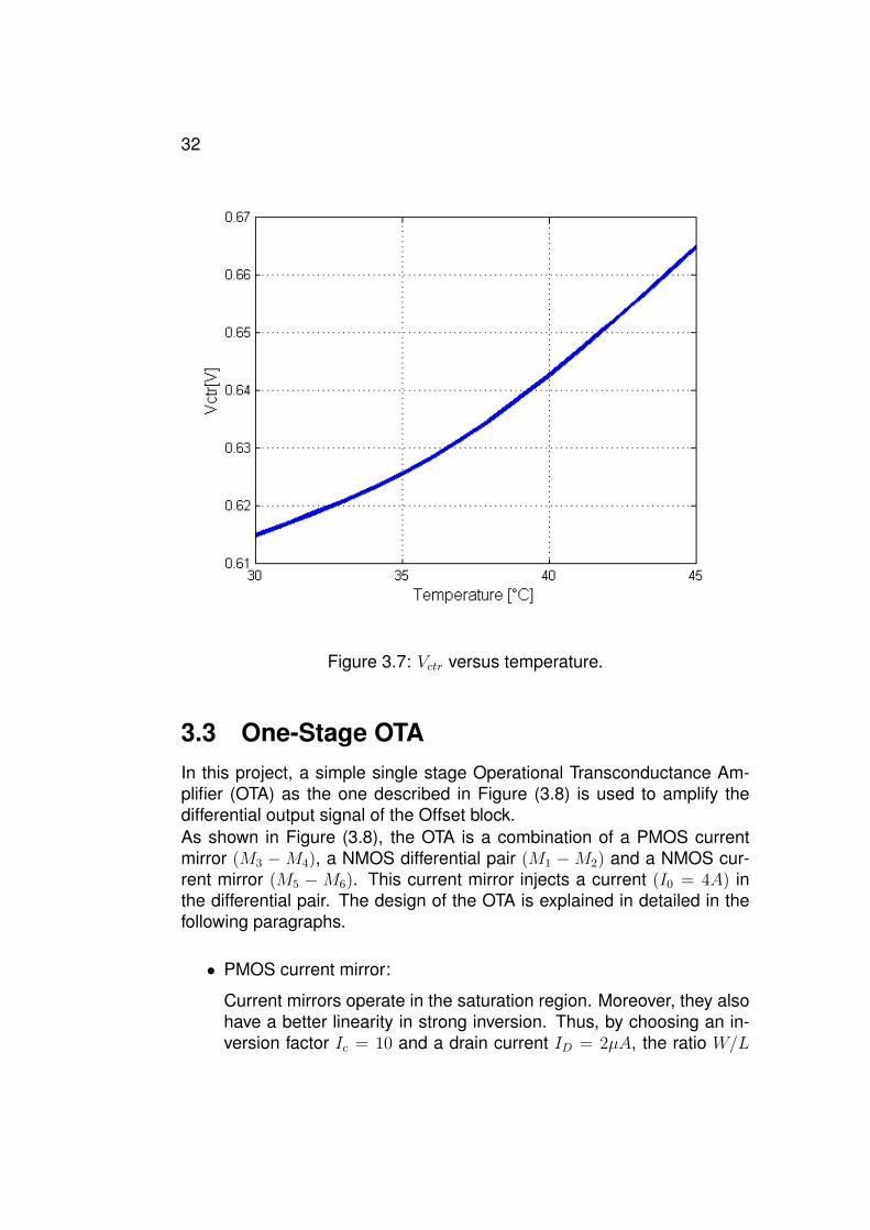
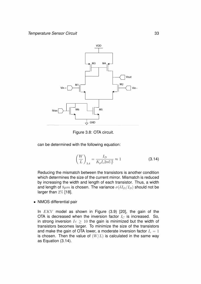
3.3 One-Stage OTAIn this project, a simple single stage Operational Transconductance Am-plifier (OTA) as the one described in Figure (3.8) is used to amplify thedifferential output signal of the Offset block.As shown in Figure (3.8), the OTA is a combination of a PMOS currentmirror (M3 −M4), a NMOS differential pair (M1 −M2) and a NMOS cur-rent mirror (M5 −M6). This current mirror injects a current (I0 = 4A) inthe differential pair. The design of the OTA is explained in detailed in thefollowing paragraphs.
• PMOS current mirror:
Current mirrors operate in the saturation region. Moreover, they alsohave a better linearity in strong inversion. Thus, by choosing an in-version factor Ic = 10 and a drain current ID = 2µA, the ratio W/L
Temperature Sensor Circuit 33
Figure 3.8: OTA circuit.
can be determined with the following equation:
(W
L
)3,4
=ID
KpIc2nU2T
≈ 1 (3.14)
Reducing the mismatch between the transistors is another conditionwhich determines the size of the current mirror. Mismatch is reducedby increasing the width and length of each transistor. Thus, a widthand length of 8µm is chosen. The variance σ(δID/ID) should not belarger than 2% [18].
• NMOS differential pair
In EKV model as shown in Figure (3.9) [20], the gain of theOTA is decreased when the inversion factor IC is increased. So,in strong inversion Ic ≥ 10 the gain is minimized but the width oftransistors becomes larger. To minimize the size of the transistorsand make the gain of OTA lower, a moderate inversion factor Ic = 1is chosen. Then the value of (W/L) is calculated in the same wayas Equation (3.14).
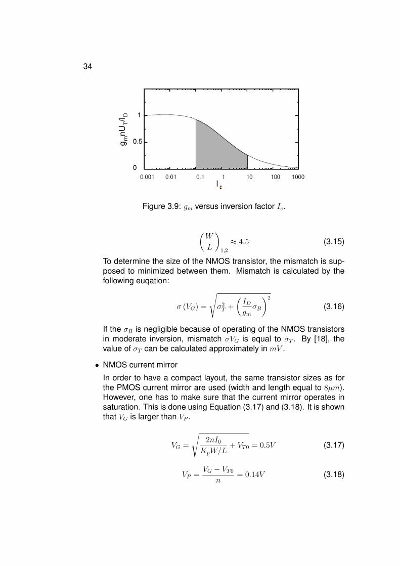
34
Figure 3.9: gm versus inversion factor Ic.
(W
L
)1,2
≈ 4.5 (3.15)
To determine the size of the NMOS transistor, the mismatch is sup-posed to minimized between them. Mismatch is calculated by thefollowing euqation:
σ (VG) =
√σ2T +
(IDgmσB
)2
(3.16)
If the σB is negligible because of operating of the NMOS transistorsin moderate inversion, mismatch σVG is equal to σT . By [18], thevalue of σT can be calculated approximately in mV .
• NMOS current mirror
In order to have a compact layout, the same transistor sizes as forthe PMOS current mirror are used (width and length equal to 8µm).However, one has to make sure that the current mirror operates insaturation. This is done using Equation (3.17) and (3.18). It is shownthat VG is larger than VP .
VG =
√2nI0
KpW/L+ VT0 = 0.5V (3.17)
VP =VG − VT0
n= 0.14V (3.18)
Temperature Sensor Circuit 35
Table (3.4) is a summary of the transistor sizes in the OTA. Additional pa-rameters such as gm and gds are also given in Table (3.5).
M1,2 M3,4 M5,6
L[µm] 1 8 8W [µm] 4.5 8 8
Table 3.4: Transistor sizes of the Offset block.
M1,2 M3,4 M5,6
gm[µS] 40.91 13.4 39, 0gds[µS] 0.549 0.0150 0.183
Table 3.5: OTA transconductance values.
The transconductance values gm and gds are used to calculate the gain,CMRR and PMRR of the OTA:
• OTA gain:
Av = gm1Rout = gm11
gds2 + gds4= 37.42dB (3.19)
• CMRR:CMRRdc =
n1gm1
gds6σgm= 1.654e−6 (3.20)
where σgm:
2σgm =
√(σVT0
n1UT
)2
+ σ2β +
(β3
n3ID
)σ2VT0
(3.21)
• PSRR
PSRR = gm1Rout = gm11
gds2 + gds4= 74.26 (3.22)
36
Table (3.6) shows a summary of the OTA characteristics:
Supply voltage 1.8VSupply current 4µA
Gain 37.42dBCMRR 1.654e−6
PSRR 74.26
Table 3.6: OTA characteristics.
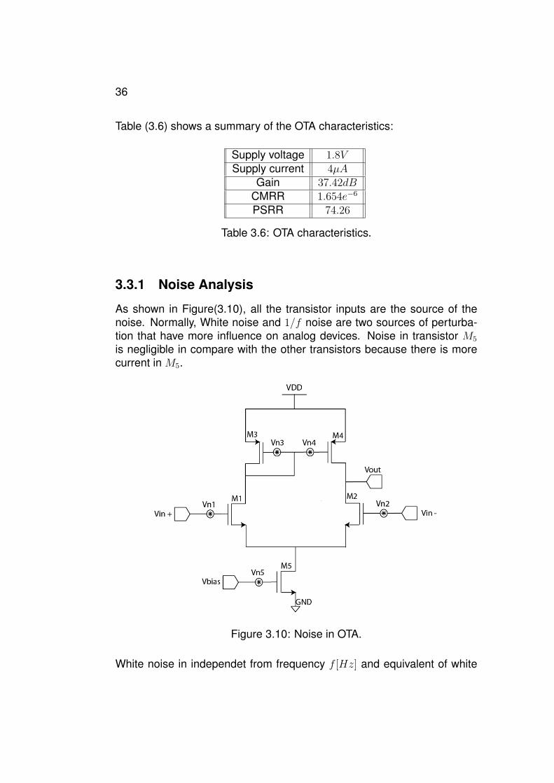
3.3.1 Noise Analysis
As shown in Figure(3.10), all the transistor inputs are the source of thenoise. Normally, White noise and 1/f noise are two sources of perturba-tion that have more influence on analog devices. Noise in transistor M5
is negligible in compare with the other transistors because there is morecurrent in M5.
Figure 3.10: Noise in OTA.
White noise in independet from frequency f [Hz] and equivalent of white
Temperature Sensor Circuit 37
noise in OTA input is witten by Equation(3.23):
V 2neq = 2V 2
n1 + 2V 2n3
(gm3
gm1
)2
(3.23)
White noise Vwneqi [V ]can be calculated in different temperature by Equa-tion(3.24):
V 2wneqi
=
(16
3
)kT
(1
gm1
)+
(16
3
)kT
(gm3
gm1
)2(1
gm1
)(3.24)
1/f noise ”Vfneqi[V/√Hz]” depends on frequency (f [Hz]):
V 2fneqi
(f) =2
Coxf
[K1
W1L1
+
(µnµp
)(K3L1
W1L23
)](3.25)
Where:
K:Filcker noise coefficient [AV/sK]
In this circuit,total noise power is addition of power of these two noisetogether.Normally White noise is negligible in compare with 1/f . So 1/fnoise is more disturbing than white noise in the circuit.
3.3.2 Offset Analysis
The offset at the input of the OTA, as depicted in Figure (3.11), can bedescribed by Equation (3.26). This offset is due to the mismatch betweenthe transistors of the OTA.
VOS,in =
(|Vgs − Vth|P
2
[∆(W/L)
W/L
]P
+ ∆Vth,P
)gmPgmN
+|Vgs − Vth|N
2
[∆(W/L)
W/L
]N
+ ∆Vth,N = 0.0059V (3.26)
In UMC 0.18µm technology, transistors can be made with a precision of10nm. Therefore, the nominal, minimum and maximum sizes of the tran-sistors in the OTA are defined in Table (3.7) .
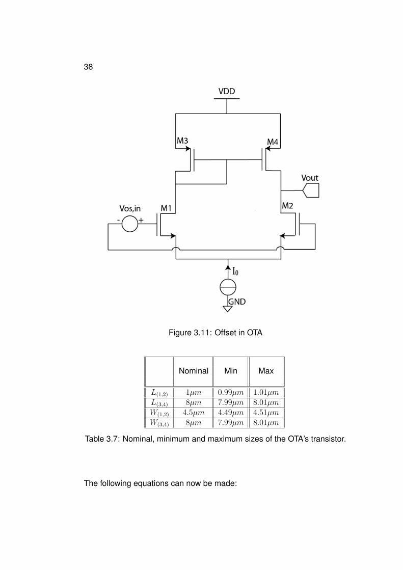
38
Figure 3.11: Offset in OTA
Nominal Min Max
L(1,2) 1µm 0.99µm 1.01µmL(3,4) 8µm 7.99µm 8.01µmW(1,2) 4.5µm 4.49µm 4.51µmW(3,4) 8µm 7.99µm 8.01µm
Table 3.7: Nominal, minimum and maximum sizes of the OTA’s transistor.
The following equations can now be made:

Temperature Sensor Circuit 39
∆(W/L)N,P = ∆(W/L)(N,P )max + ∆(W/L)(N,P )min
∆(W/L)N =4.51
0.99− 4.49
1.01= 0.11
∆(W/L)P =8.01
7.99− 7.99
8.01= 0.005[
∆(W/L)
W/L
]N
=0.11
4.5= 0.0244[
∆(W/L)
W/L
]P
=5e−3
1= 0.005
In UMC 0,18 µm ,∆VTh,n and ∆VTh,p are calculated as follow:
∆VTh,n = 3(rDVth,n)WL
= 100.5
= 3× 1.6968e−3
∆VTh,p = 3(rDVth,p)WL
= 103
= 3× 0.4207e−3
The other parameters which are used to calculate VOS,in are given in Table(3.8) and Table (3.5).
Vgsp[V ] Vgsn[V ] VT0p[V ] VT0n [V ]−0.72314 0.495 −0.4558 0.48179
Table 3.8: Parameters for calculating the offset of the OTA.
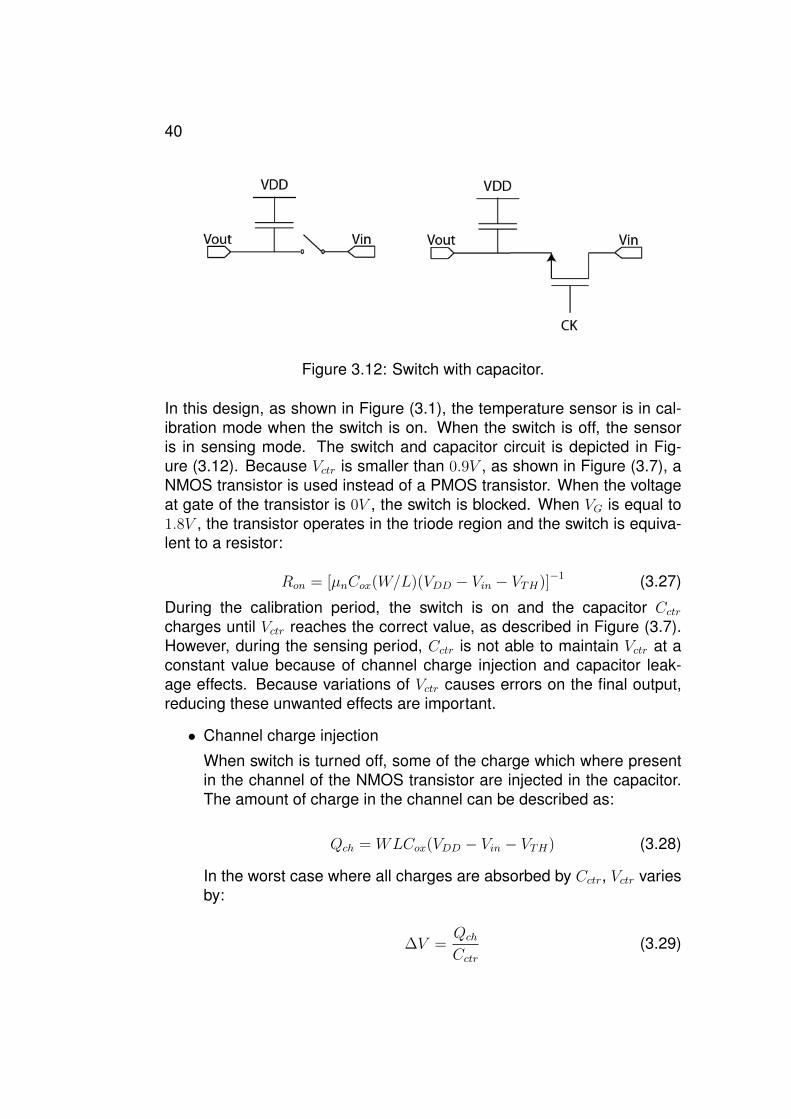
3.4 Switch and Capacitor
During electrophysiological experiments, the first step that has to beundertaken is the calibration of the temperature sensor. This means thatwhen the MEA is taken out of its incubator for measurements, calibrationhas to be performed before the MEA cools down. However, it has beenshown in Section 2.3 that the time constant of the function Tsensor/Tamb isequal to about 10 min, which leaves us some time to perform calibration.
40
Figure 3.12: Switch with capacitor.
In this design, as shown in Figure (3.1), the temperature sensor is in cal-ibration mode when the switch is on. When the switch is off, the sensoris in sensing mode. The switch and capacitor circuit is depicted in Fig-ure (3.12). Because Vctr is smaller than 0.9V , as shown in Figure (3.7), aNMOS transistor is used instead of a PMOS transistor. When the voltageat gate of the transistor is 0V , the switch is blocked. When VG is equal to1.8V , the transistor operates in the triode region and the switch is equiva-lent to a resistor:
Ron = [µnCox(W/L)(VDD − Vin − VTH)]−1 (3.27)
During the calibration period, the switch is on and the capacitor Cctrcharges until Vctr reaches the correct value, as described in Figure (3.7).However, during the sensing period, Cctr is not able to maintain Vctr at aconstant value because of channel charge injection and capacitor leak-age effects. Because variations of Vctr causes errors on the final output,reducing these unwanted effects are important.
• Channel charge injection
When switch is turned off, some of the charge which where presentin the channel of the NMOS transistor are injected in the capacitor.The amount of charge in the channel can be described as:
Qch = WLCox(VDD − Vin − VTH) (3.28)
In the worst case where all charges are absorbed by Cctr, Vctr variesby:
∆V =Qch
Cctr(3.29)
Temperature Sensor Circuit 41
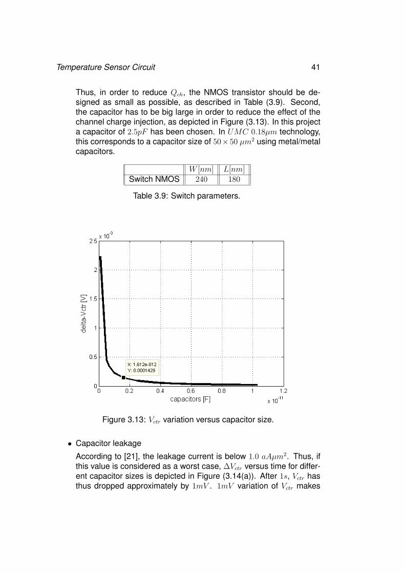
Thus, in order to reduce Qch, the NMOS transistor should be de-signed as small as possible, as described in Table (3.9). Second,the capacitor has to be big large in order to reduce the effect of thechannel charge injection, as depicted in Figure (3.13). In this projecta capacitor of 2.5pF has been chosen. In UMC 0.18µm technology,this corresponds to a capacitor size of 50×50 µm2 using metal/metalcapacitors.
W [nm] L[nm]Switch NMOS 240 180
Table 3.9: Switch parameters.
Figure 3.13: Vctr variation versus capacitor size.
• Capacitor leakage
According to [21], the leakage current is below 1.0 aAµm2. Thus, ifthis value is considered as a worst case, ∆Vctr versus time for differ-ent capacitor sizes is depicted in Figure (3.14(a)). After 1s, Vctr hasthus dropped approximately by 1mV . 1mV variation of Vctr makes
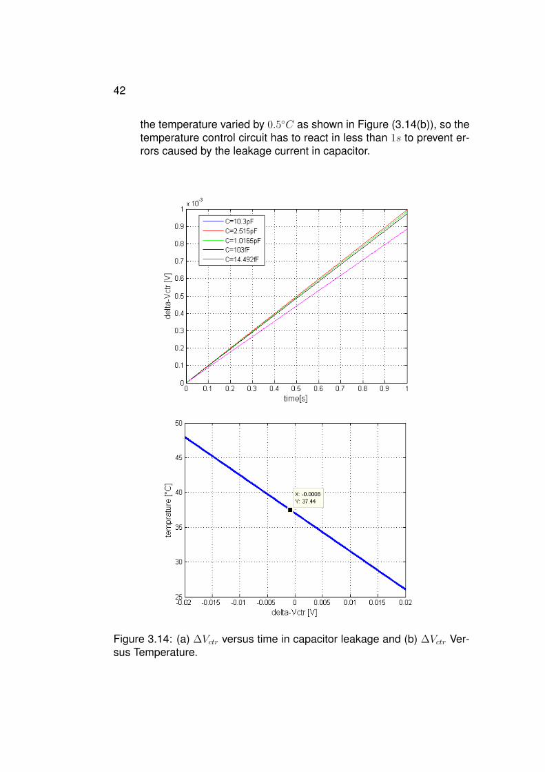
42
the temperature varied by 0.5◦C as shown in Figure (3.14(b)), so thetemperature control circuit has to react in less than 1s to prevent er-rors caused by the leakage current in capacitor.
Figure 3.14: (a) ∆Vctr versus time in capacitor leakage and (b) ∆Vctr Ver-sus Temperature.
Temperature Sensor Circuit 43
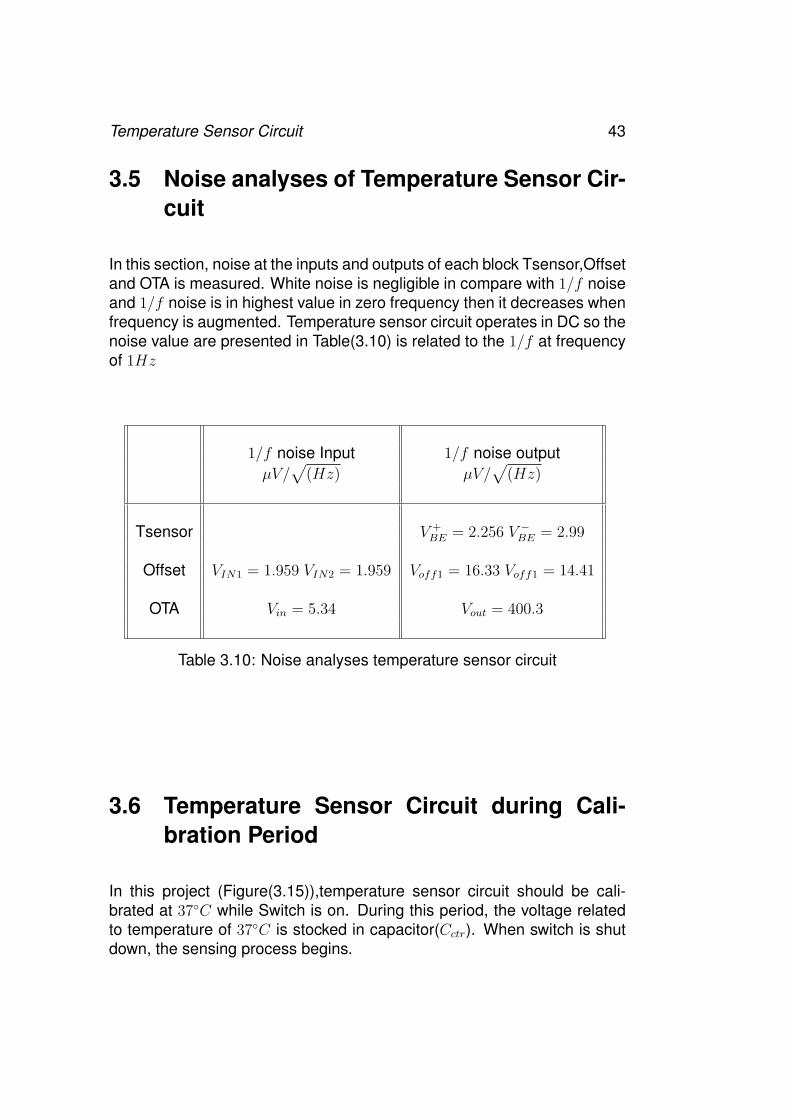
3.5 Noise analyses of Temperature Sensor Cir-cuit
In this section, noise at the inputs and outputs of each block Tsensor,Offsetand OTA is measured. White noise is negligible in compare with 1/f noiseand 1/f noise is in highest value in zero frequency then it decreases whenfrequency is augmented. Temperature sensor circuit operates in DC so thenoise value are presented in Table(3.10) is related to the 1/f at frequencyof 1Hz
1/f noise Input 1/f noise outputµV/
√(Hz) µV/
√(Hz)
Tsensor V +BE = 2.256 V −BE = 2.99
Offset VIN1 = 1.959 VIN2 = 1.959 Voff1 = 16.33 Voff1 = 14.41
OTA Vin = 5.34 Vout = 400.3
Table 3.10: Noise analyses temperature sensor circuit
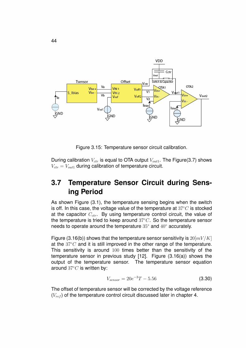
3.6 Temperature Sensor Circuit during Cali-bration Period
In this project (Figure(3.15)),temperature sensor circuit should be cali-brated at 37◦C while Switch is on. During this period, the voltage relatedto temperature of 37◦C is stocked in capacitor(Cctr). When switch is shutdown, the sensing process begins.
44
Figure 3.15: Temperature sensor circuit calibration.
During calibration Vctr is equal to OTA output Vout1. The Figure(3.7) showsVctr = Vout1 during calibration of temperature circuit.
3.7 Temperature Sensor Circuit during Sens-ing Period
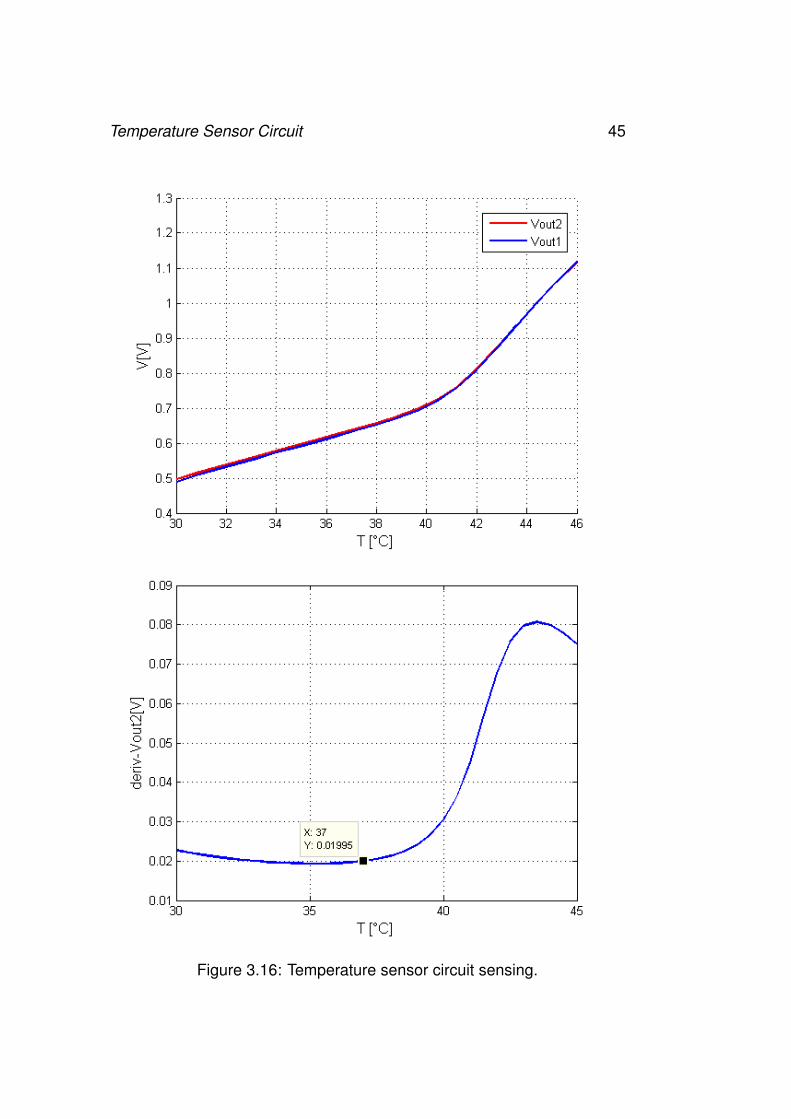
As shown Figure (3.1), the temperature sensing begins when the switchis off. In this case, the voltage value of the temperature at 37◦C is stockedat the capacitor Cctr. By using temperature control circuit, the value ofthe temperature is tried to keep around 37◦C. So the temperature sensorneeds to operate around the temperature 35◦ and 40◦ accurately.
Figure (3.16(b)) shows that the temperature sensor sensitivity is 20[mV/K]at the 37◦C and it is still improved in the other range of the temperature.This sensitivity is around 100 times better than the sensitivity of thetemperature sensor in previous study [12]. Figure (3.16(a)) shows theoutput of the temperature sensor. The temperature sensor equationaround 37◦C is written by:
Vsensor = 20e−3T − 5.56 (3.30)
The offset of temperature sensor will be corrected by the voltage reference(Vref ) of the temperature control circuit discussed later in chapter 4.
Temperature Sensor Circuit 45
Figure 3.16: Temperature sensor circuit sensing.
46
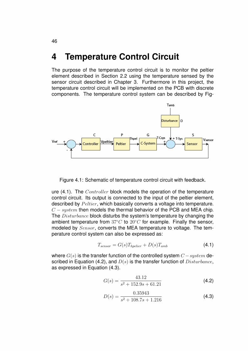
4 Temperature Control CircuitThe purpose of the temperature control circuit is to monitor the peltierelement described in Section 2.2 using the temperature sensed by thesensor circuit described in Chapter 3. Furthermore in this project, thetemperature control circuit will be implemented on the PCB with discretecomponents. The temperature control system can be described by Fig-
Figure 4.1: Schematic of temperature control circuit with feedback.
ure (4.1). The Controller block models the operation of the temperaturecontrol circuit. Its output is connected to the input of the peltier element,described by Peltier, which basically converts a voltage into temperature.C − system then models the thermal behavior of the PCB and MEA chip.The Disturbance block disturbs the system’s temperature by changing theambient temperature from 37◦C to 20◦C for example. Finally the sensor,modeled by Sensor, converts the MEA temperature to voltage. The tem-perature control system can also be expressed as:
Tsensor = G(s)Thpelier +D(s)Tamb (4.1)
where G(s) is the transfer function of the controlled system C−system de-scribed in Equation (4.2), and D(s) is the transfer function of Disturbance,as expressed in Equation (4.3).
G(s) =43.12
s2 + 152.9s+ 61.21(4.2)
D(s) =0.35943
s2 + 108.7s+ 1.216(4.3)
Temperature Control System 47
The transform function of the peltier element P is described in Equation(4.4) using Figure (2.10). The transfer function S of the temperature sensorcan also be expressed as in Equation (4.5).
P =ThpeltierVpeltier
= 60.24[◦C,K/V ] (4.4)
S =VsensorTsys
= 20e−3[V/◦C,K] (4.5)
As shown in Figure (4.1), the temperature control system is connected inclosed loop in order to keep the temperature of the circuit at 37◦C. Theaim of using a controller with feedback is to decrease the sensitivity of thesystem against the ambient disturbance. Thus, the rejection of disturbanceis improved with this control system. The equation of the temperaturecontrol circuit in close loop is written as:
Vsensor =C(s)PG(s)S
1 + C(s)PG(s)SV ref +
D(s)S
1 + C(s)PG(s)STamb (4.6)
As explained in the following Section, the controller PI, is designed for thissystem.
4.1 PI ControllerIn This project, A Proportional-Integral(PI) controller is designed insteadof Proportional-Integral-derivative (PID) controller because of the followingreasons: First, time constant of the derivative device Td is relatively smalland it is equal 0.0065s calculated by [22] and seeing Equation (4.8):
Td =τ1τ2
τ1 + τ2
= 0.0065 (4.7)
So the PID response to an unity step input is almost same as the responseof the PI to this input.Second, rising the time constant of the derivative device is caused over-shooting and unexpected oscillation which are not favorable for stability ofcontroller.Third, implementation of PI is easier than the implementation of PID.
In order to design a Proportional-Integral (PI) controller, transfer functionG(s) described in Equation (4.2) is decomposed and written as:
G(s) =0.7045
(0.0066s+ 1) (2.4913s+ 1)=
b
(τ1s+ 1)(τ2s+ 1)(4.8)
48
A PI controller is calculated by the following equation [22]:
C(s) =τ1 + τ2
bτc
(1 +
1
(τ1 + τ2)s
)(4.9)
Ti[s] is the integrator time constant.
Ti = τ1 + τ2 = 2.4978 (4.10)
Kp: Gain of controller with Equation(4.11)
Kp =τ1 + τ2
bτc(4.11)
with τc[s] time constant of controller or time for response to step.
G(s) is in series with Sensor and Peltier.So the gain of Sensor Sand peltier P is multiplied to the gain of controller Kp. For having acontroller gain independent of the peltier and sensor gains the gain ofcontroller Kptot is calculated by the Equation(4.12)
Kptot =Kp
SP(4.12)
By Figure(3.14 (a),and (b)),voltage in capacitor is changed by 1mV after1s, which is caused the temperature variation about 0.5◦C. To prevent thetemperature control errors due to wrong temperature sensing, the settlingtime for PI controller is supposed to be less than the 1s and steady-stateerror should be less than the 1mV .
Temperature Control System 49
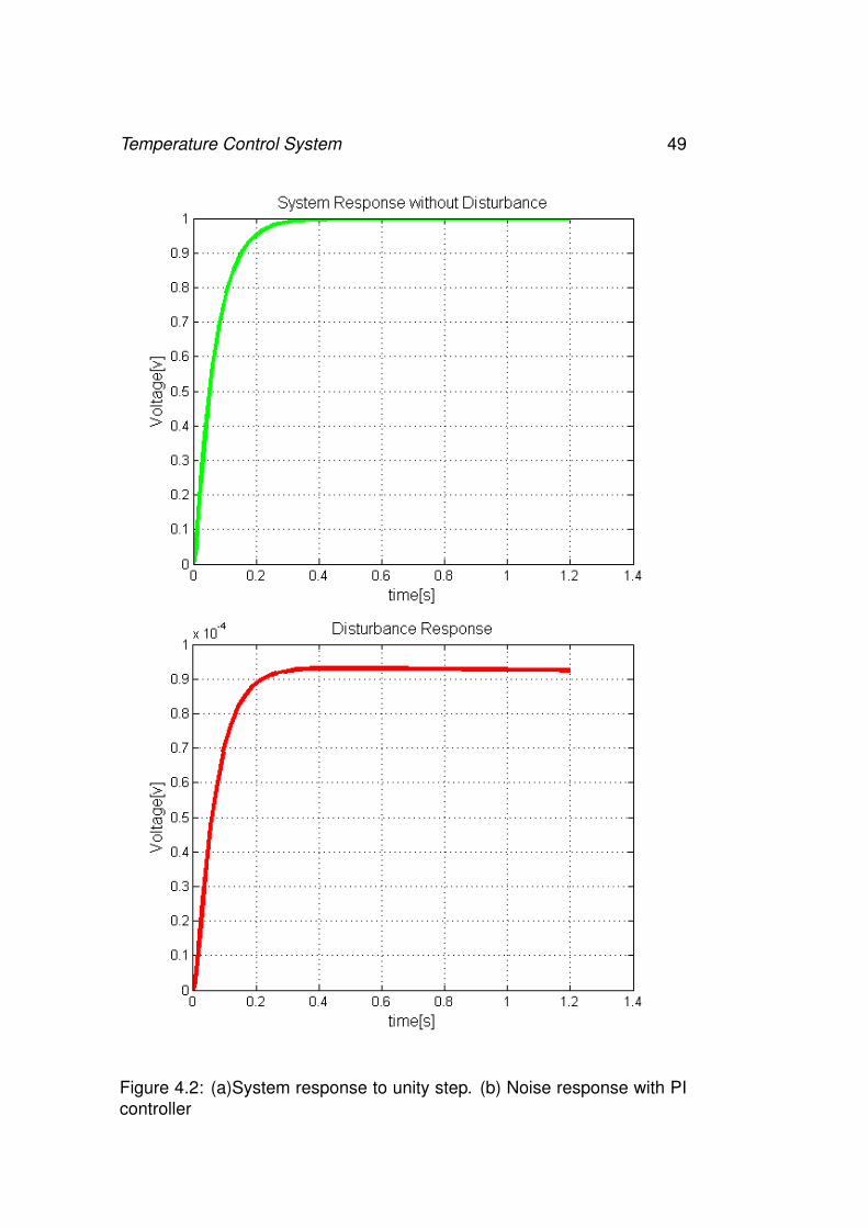
Figure 4.2: (a)System response to unity step. (b) Noise response with PIcontroller
50
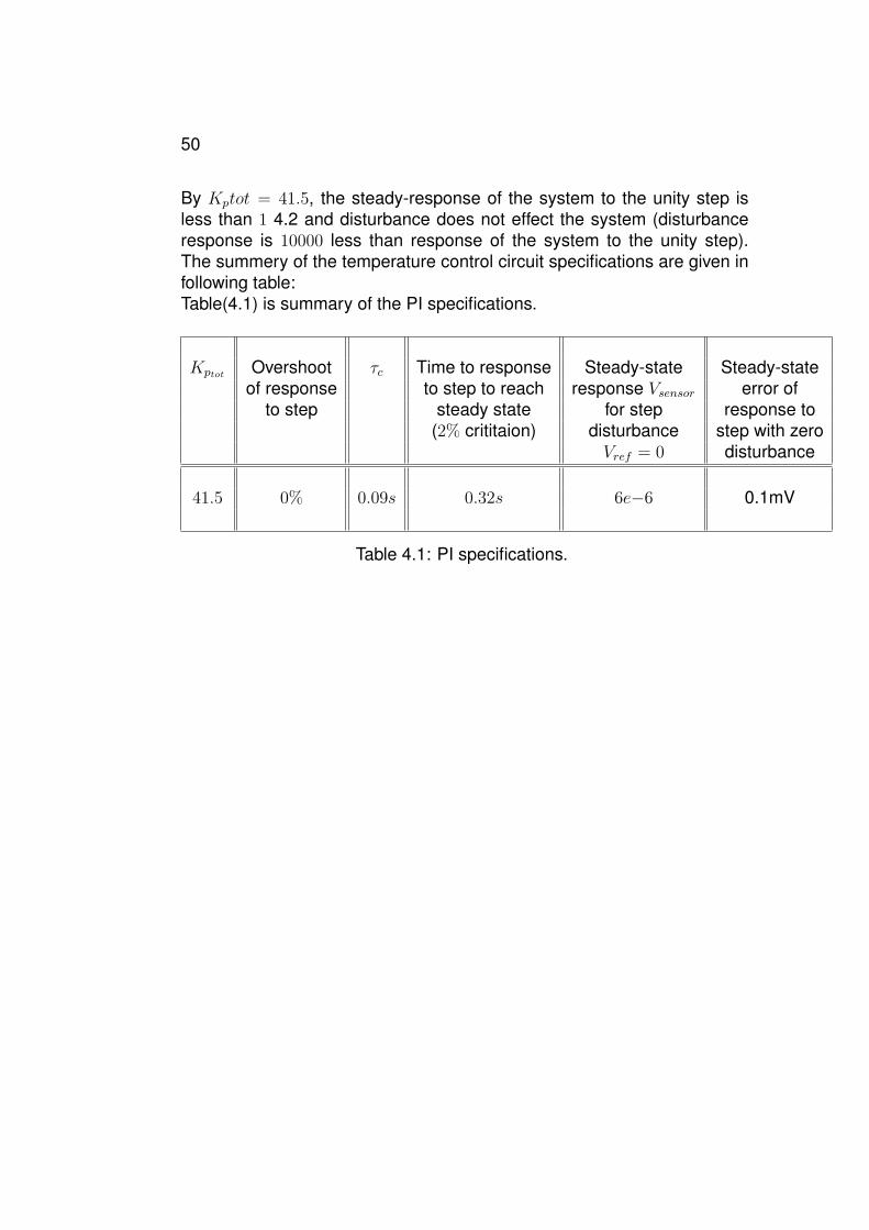
By Kptot = 41.5, the steady-response of the system to the unity step isless than 1 4.2 and disturbance does not effect the system (disturbanceresponse is 10000 less than response of the system to the unity step).The summery of the temperature control circuit specifications are given infollowing table:Table(4.1) is summary of the PI specifications.
Kptot Overshoot τc Time to response Steady-state Steady-stateof response to step to reach response Vsensor error of
to step steady state for step response to(2% crititaion) disturbance step with zero
Vref = 0 disturbance
41.5 0% 0.09s 0.32s 6e−6 0.1mV
Table 4.1: PI specifications.
Conclusion and Future Perspective 51
5 Conclusion and Future Perspective
5.1 AchievementAfter having introduced MEA systems and some related work on thedesign of temperature control systems for MEAs, the thermal model ofMEA chips has been developed. This model has theoretically proventhat the temperature of the cell culture can be maintained at a constanttemperature of 37◦C in real time. However, aluminum vias need to beimplemented in the PCB in order to better transfer the heat flow.
A temperature sensor has been designed at the schematic level. Itspurpose is to measure the temperature of the neural cells during elec-trophysiological experiments. An offset cancellation circuit has beenimplemented in the circuit in order to increase the sensitivity of the sensor.A sensitivity of 20[mV/K] has been obtained in the rage of 35◦C to 40◦C.
Finally, preliminary work on the design of temperature control circuithas been performed. This circuit reacts to temperature variations inaround 1 sec in order to maintain the temperature of the cell culture at37◦C.
5.2 Future WorkThe layout of the CMOS temperature sensor has to be designed. Afterthat, the specifications of the temperature sensor need to be verified dur-ing post-layout simulations. The temperature control circuit is currently be-ing designed based on the simulation results obtained in Chapter 4. Thiscircuit will be implemented on the PCB with discrete elements. Finally,the operation of the temperature control system needs to be verified andcharacterize during in-vitro electrophysiological experiments.
EPFL,15 January 2010
Mona FARSAD
52
References[1] S. Marom and G. Shahaf, “Development, learning and memory in
large random networks of cortical neurons: lessons beyond anatomy,”Quarterly Reviews of Biophysics, vol. 35, no. 1, pp. 63–78, May 2002.
[2] A. Stett, U. Egert, E. Guenther, F. Hofmann, T. Meyer, W. Nisch,and H. Haemmerle, “Biological application of microelectrode arraysin drug discovery and basic research,” Anal Bioanal Chem, vol. 377,no. 3, pp. 486–495, 2003.
[3] J. Aziz, R. Karakiewicz, R. Genov, A. W. L. Chiu, B. L. Bardakjian,M. Derchansky, and P. L. Carlen, “On-silicon neural activity monitoringand time-frequency analysis for early detection of epileptic seizures,”IEEE Trans. Neural Syst. Rehabil. Eng., submitted.
[4] L. Cozzi, P. D’Angelo, V. Sanguineti, A. Novellinoand, S. Martinoia,L. Berdondini, and M. Koudelka-Hep, “Towards natural computation:reactive control of a mobile robot by a population of cultured neurons,”Proc. BioRob, pp. 525–530, 2006.
[5] “Multi Channel Systems MCS GmbH.” http://
multichannelsystems.com.
[6] W. L. C. Rutten, “Selective electrical interfaces with the nervous sys-tem,” Annu. Rev. Biomed.Eng., vol. 4, pp. 407–452, 2002.
[7] B. Eversmann, M. Jenkner, F. Hofmann, C. Paulus, R. Brederlow,B. Holzapfl, P. Fromherz, M. Merz, M. Brenner, M. Schreiter, R. Gabl,K. Plehnert, M. Steinhauser, G. Eckstein, D. Schmitt-Landsiedel, andR. Thewes, “A 128 x 128 CMOS biosensor array for extracellularrecording of neural activity,” IEEE J. Solid-State Circuits, vol. 38,pp. 2306–2317, Dec. 2003.
[8] U. Frey, F. Heer, R. Pedron, S. Hafizoic, F. Greve, J. Sedivy, K. U.Kirstein, and A. Hierlemann, “An 11k-electrode 126-channel high-density microelectrode array to interact with electrogenic cells,” inProc. IEEE ISSCC, pp. 158–593, 2007.
[9] K. Imfeld, S. Neukom, A. Maccione, Y. Bornat, S. Martinoia, P. A.Farine, M. Koudelka-Hep, and L. Berdondini, “Large-scale, high-resolution data acquisition system for extracellular recording of elec-trophysiological activity,” IEEE Trans. Biomed. Eng, vol. 55, pp. 2064–2073, 2008.
References 53
[10] N. Joye, A. Schmid, and Y. Leblebici, “Three-dimensional silicon-based MEA with high spatial resolution,” Proc. 6th Int. Meeting onSubstrate-Integrated Microelectrodes, pp. 310–311, 2008.
[11] N. Joye, A. Schmid, and Y. Leblebici, “Electrical modeling of the cell-electrode interface for recording neural activity from high-density mi-croelectrode arrays,” Neurocomputing, vol. 73, pp. 250–259, Dec.2009.
[12] F. Heer, CMOS-based microelectrode array for communication withelectrogenic cells. PhD thesis, ETHZ, 2005.
[13] K. H. Gilchrist, V. N. Barker, L. E. Fletcher, B. D. DeBusschere,P. Ghanouni, L. Giovangrandi, and G. T. A. Kovacs, “General pur-pose, field-portable cell-based biosensor platform,” Biosensors andBioelectronics, vol. 16, pp. 557–564, 2001.
[14] J. Christen and A. Andreou, “Design, Fabrication, and Testing of aHybrid CMOS/PDMS Microsystem for Cell Culture and Incubation,”IEEE Trans. Biomedical Circuits and Systems, vol. 1, pp. 3–18, March2007.
[15] G. Blackwell, “Thermal Management,” in The Electronic PackagingHandbook, Ed. C. R. Blackwell, CRC Press LLC, 2000.
[16] Formulaires et Tables. Ed. du Tricone, Geneve, 1985.
[17] A. Andonova, N. Kafadarova, V. Videkov, and S. Andreev, “Investi-gation of thermal conductivity of PCB,” Proc. Int. Spring Seminar onElectronics Technology (ISSE), pp. 13–17, 2009.
[18] ”0.18µm Mixed-Mode 1.8V Process Matching Report”. Ver. 2.0-P.1,Approve Date 20/01/2009. UMC CONFIDENTIAL, NO DISLOSURE.
[19] M. Vadipour, “Optimum degeneration for minimum mismatch in bipo-lar current sources,” IEEE J. Solid-State Circuits, vol. 29, no. 10,pp. 1297–1300, 1994.
[20] C. Enz, F. Krummenacher, and E. A. Vittoz, “An Analitical MOS Tran-sistor Model Valid in All Regions of Operation and Dedicated to Low-Voltage and Low-Current Applications,” J. Analog Integrated Circuitsand Signal Processing, vol. 8, pp. 83–114, July 1999.

54
[21] ” 0.18µm Mixed-Mode Process Al Metal Metal Capacitor Characteri-zation Report”. Ver. 2.0-P.1, Approve Date 04/02/2009. UMC CON-FIDENTIAL, NO DISCLOSURE.
[22] R. Longchamp, Commande Numerique de Systemes Dynamiques.Presses Polytechniques et Universitaires Romandes, second ed.,2006.