Embed Size (px)
Citation preview

407
Chapter 16
Microelectrode electronics
DAVID OGDEN
1. Introduction
These notes are intended to provide an introduction to the electronics ofmicroelectrode and patch clamp amplifiers. How much electronics do you need to usea physiological amplifier? Enough to know how much distortion is introduced by themeasurement. This means (1) testing the response to an input that simulates thephysiological signal, (2) calibrating the gain and frequency response, and (3)knowing the errors that might arise from limited performance. This ‘black box’approach to instruments is the minimum needed and requires a knowledge of thebasic principles of electronic circuits. It is fine until something goes wrong or aspecial requirement arises which prompts a look inside to see how things work andwhether a modification can be made.
It is worthwhile taking a practical course in e.g. medical electronics if one isavailable and working in the electronics workshop for a period to learn solderingfrom an expert. For those interested in making circuits, applications are given belowof operational amplifiers in circuits which may be useful for signal processing andcan be built relatively easily and cheaply. Building operational amplifier circuits is avery good way of learning the basics of electronics - the amplifiers commonly usedare inexpensive enough to permit a degree of trial and error and standard printedcircuit boards are available.
A knowledge of the properties and jargon of low-pass filters is necessary forsurvival. These are introduced and their use prior to digitizing data for computeranalysis is discussed.
Many topics have not been included and for these, and wider coverage of topicsintroduced here, a list of books and articles for further reading and reference isappended.
Current flow in resistors and capacitorsCurrent, units Amps, is the rate at which charge (measured in Coulombs) flows at apoint in a circuit. The driving potential, measured in Volts, is the energy of each unitof charge, Joules/Coulomb, and is analogous to pressure in a gas or concentration insolution. The conversion between chemical concentration of charged particles andelectrical quantities of charge is by the Faraday, about 96500 Coulombs/mole ofunivalent ion, so 96.5 nA of current flowing in a solution is carried by a flux of 1picomole of univalent ions/s.
National Institute for Medical Research, Mill Hill, London NW7 1AA, UK

Resistance and conductance.Charge flows through a wire, a solution or otherconductive media by the movement of charged particles, electrons or ions, againstresistance imposed by random thermal motion. The reciprocal of resistance isconductance.
Current flow in a resistoris proportional to the voltage applied across theterminals. Resistance is measured as 1 Ohm, Ω = 1 Volt/Amp. Conductance,Amp/Volt, is measured in Siemens, S = 1/Ohm.
Capacitance.Charges accumulate where two conductors are in close contact (acapacitor) and at different voltages. Energy is stored by polarisation of the medium(the dielectric) between the conductors. The charge accumulated is proportional tothe voltage applied, and charges move into and out of the conductors when thevoltage changes.
Current flow in a capacitoris proportional to the rate of changeof voltage, Amps =capacitance × dV/dt. As a consequence the presence of capacitance modifies thetimecourse of potential with respect to current flow.
The unit of capacitance measures the accumulation of charge for 1 volt change ofpotential, 1 Farad = 1 Coulomb/Volt.
Electrical models of the properties of cells and tissues comprise networks ofresistors and capacitors, the former representing paths for current along the core andthrough ion channels in the surface membrane and the latter capacitative flow acrossthe nonconducting lipid bilayer. No charges (ions) physically cross the membranecapacitor, but flow in the adjacent solution as the membrane potential fluctuates.
Time course of capacitor charging. The single most important circuit for anelectrophysiologist is the charging, or discharge, of a capacitor through a resistor. Fora voltage V applied to a resistor and capacitor in series, the voltage measured acrossthe capacitor, VC, can be derived as follows.
Assume (1) that the applied voltage can supply enough current (i.e. has negligableinternal resistance) and (2) that the voltage measurement draws no current from thecircuit.
Current flowing into the capacitor is supplied via the resistor, so currents flowinginto the junction (defined positive) of R and C, where the voltage across the capacitoris measured, are
iC + iR = 0.
•• •
•
•
•
V
R
C
iR
iC
VC
408 D. OGDEN
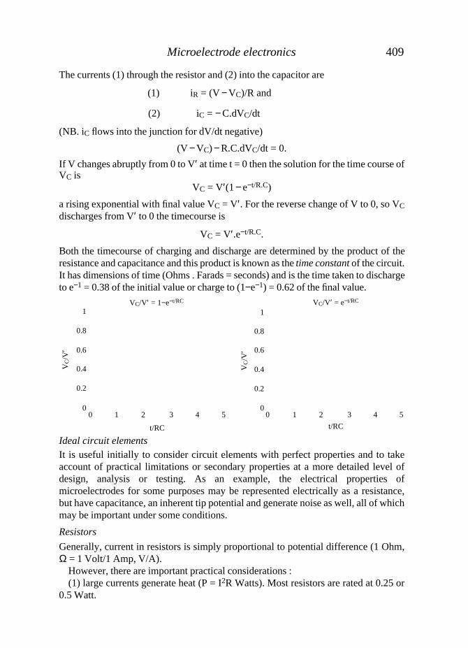
The currents (1) through the resistor and (2) into the capacitor are
(1) iR = (V −VC)/R and
(2) iC = −C.dVC/dt
(NB. iC flows into the junction for dV/dt negative)
(V −VC) −R.C.dVC/dt = 0.
If V changes abruptly from 0 to V′ at time t = 0 then the solution for the time course ofVC is
VC = V′(1−e−t/R.C)
a rising exponential with final value VC = V′. For the reverse change of V to 0, so VC
discharges from V′ to 0 the timecourse is
VC = V′.e−t/R.C.
Both the timecourse of charging and discharge are determined by the product of theresistance and capacitance and this product is known as the time constantof the circuit.It has dimensions of time (Ohms . Farads = seconds) and is the time taken to dischargeto e−1 = 0.38 of the initial value or charge to (1−e−1) = 0.62 of the final value.
Ideal circuit elementsIt is useful initially to consider circuit elements with perfect properties and to takeaccount of practical limitations or secondary properties at a more detailed level ofdesign, analysis or testing. As an example, the electrical properties ofmicroelectrodes for some purposes may be represented electrically as a resistance,but have capacitance, an inherent tip potential and generate noise as well, all of whichmay be important under some conditions.
Resistors
Generally, current in resistors is simply proportional to potential difference (1 Ohm,Ω = 1 Volt/1 Amp, V/A).
However, there are important practical considerations : (1) large currents generate heat (P = I2R Watts). Most resistors are rated at 0.25 or
0.5 Watt.
0.8
0.6
0.4
0.2
0
1
VC/V
′
1 2 3 4 50
t/RC
VC/V′ = 1−e−t/RC VC/V′ = e−t/RC
0.8
0.6
0.4
0.2
0
1
VC/V
′
2 3 4 50 1
t/RC
409Microelectrode electronics

(2) Resistors have capacitance across the terminals (~0.1-1 pF) which may beimportant with high resistances (>10 MΩ) and fast voltage changes (e.g. a step ofpotential) because current will flow through the capacitance as the voltage changesquickly to its new value, producing an initial spike of current.
(3) Voltage noise in resistors has a component (Johnson noise) which increaseswith the value of resistance, plus an additional component that depends on the resistorcomposition and voltage difference applied. The rms (standard deviation) of Johnsonnoise is V(rms)=(4kTfcR)0.5 (k is Boltzmanns constant 1.36×10⁻⁹ Joule/degree, Ttemperature °Kelvin, R resistance, Ω, and fc the bandwidth, Hz).
(4) Moisture or dirt/grease may conduct appreciable current across high valueresistors (>100 MΩ).
(5) Commonly, resistor tolerances are 5% or 2% - more precise values can be selected(with a digital multimeter, DMM) or obtained with 2 resistors in series or parallel.
Capacitors
The charge, Q (Coulombs), accumulated on the plates of a capacitor is proportional tothe potential difference, V, between the plates, Q=C.V, where the capacitance C hasdimensions of Farads (F). The energy difference between the plates due to thepotential difference (Volts=Joules/Coulomb) is absorbed in the insulating dielectricseparating the plates. No current flows between the plates of an ideal capacitor, but ifthe voltage changes then current, i, flows into the plates as the charge accumulatedchanges (Amp=Coulomb/s). Practically, some types of capacitor, such as the largevalue electrolytic types used in power supplies, may have small leakage currentsacross the plates. Some types distort rapidly changing signals due to the poorproperties of the dielectric, and should not be used where fast signals are encountered.Tolerances are usually 20%. Precise measurement of capacitance is much moredifficult than the measurement of resistance.
2. Voltage measurement
The circuit below represents the generation and measurement of a potential and canbe split into 3 sections:
A. Source of voltage.The potential V is developed across the output of a voltagegenerator represented by an ideal voltage source E in series with a small output
410 D. OGDEN
resistance Ro. Although E produces a constant voltage even if very large currents aregenerated, the output voltage V is reduced by an amount (E−V)=IRo; this is thesituation in real voltage generators, where Ro may represent the internal resistance ofa battery or the output impedance of an amplifier. These are normally small (<10 Ω)and only become important at relatively large currents (>100 mA). However, thesame considerations apply to microelectrode recording, where E may represent thecell membrane potential and Ro the electrode resistance (> 10 MΩ), so large errors(E−V) may result from small currents (>10 pA).
B. The measuring circuitconsists of 3 elements, an ideal voltmeter, which draws nocurrent from the circuit and responds instantly to potential changes at the input, aresistance Rin to account for current flowing in the input in response to the input voltage,and a capacitance Cin. The current drawn by the input is V/Rin and determines the errorin measuring E, (E−V) = Ro.V/Rin, so V/E = Rin/ (Ro+Rin). The input resistance, Rin, ofan oscilloscope amplifier is often 1 MΩ or 10 MΩ, of a microelectrode amplifier 1012Ωand of a pH meter 1014 Ω. It is clearly important that Rin»Ro to minimize the error inpotential measurements. The input capacitance contributes to slowing the response to achange of V, to an extent that depends on Cin and Rin; the output for a step input is anexponential of time constant τ = Cin.RinRo/(Rin + Ro) (see below).
C. The connectionbetween voltage generator and measuring instrument usuallyinvolves a wire of low resistance, but often with important stray capacitance toground. In the case of screened cable (with braided copper shield connected to earth)this amounts to 100-200 pF/m and may restrict the speed of transmitted signals if it isinseries with a large output impedence. A second effect of this capacitance may be toproduce instability in the output of an operational amplifier, requiring insertion of aresistor of 20-50 Ω at Ro to limit the current flowing into the capacitance in fastsignals. In the case of a microelectrode or other high resistance source, the straycapacitance should be kept as small as possible by using short connections betweenthe electrode and amplifier input, as discussed below.
3. Rules for circuit analysis
There are two basic rules; (1) currents flowing into a node sum to zero, so in theexample shown
411Microelectrode electronics
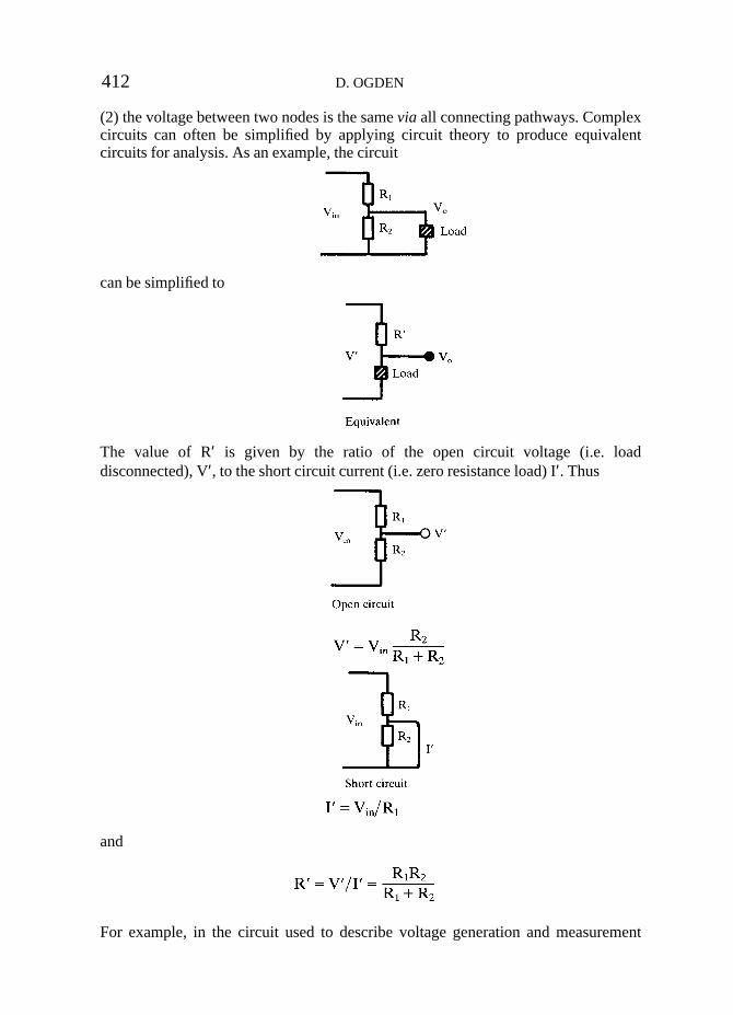
(2) the voltage between two nodes is the same via all connecting pathways. Complexcircuits can often be simplified by applying circuit theory to produce equivalentcircuits for analysis. As an example, the circuit
can be simplified to
The value of R′ is given by the ratio of the open circuit voltage (i.e. loaddisconnected), V′, to the short circuit current (i.e. zero resistance load) I′. Thus
and
For example, in the circuit used to describe voltage generation and measurement
412 D. OGDEN
above, the load can be represented by the parallel capacitors Cin+Cs=C. Theequivalent potential and resistance are given by
and the charging time constant by τ=R′C. The time course of the potential measured,V(t), following a step change of E at t=0, is given by
V(t) = V′[1 − e−t/R′C]
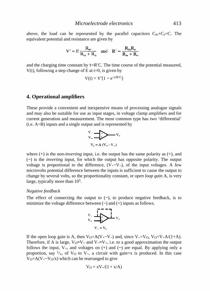
4. Operational amplifiers
These provide a convenient and inexpensive means of processing analogue signalsand may also be suitable for use as input stages, in voltage clamp amplifiers and forcurrent generation and measurement. The most common type has two ‘differential’(i.e. A−B) inputs and a single output and is represented by
where (+) is the non-inverting input, i.e. the output has the same polarity as (+), and(−) is the inverting input, for which the output has opposite polarity. The outputvoltage is proportional to the difference, (V+−V−), of the input voltages. A fewmicrovolts potential difference between the inputs is sufficient to cause the output tochange by several volts, so the proportionality constant, or open loop gainA, is verylarge, typically more than 105.
Negative feedback
The effect of connecting the output to (−), to produce negative feedback, is tominimize the voltage difference between (−) and (+) inputs as follows.
If the open loop gain is A, then VO=A(V+−V−) and, since V−=VO, VO=V+A/(1+A).Therefore, if A is large, VO≈V+ and V−≈V+, i.e. to a good approximation the outputfollows the input, V+, and voltages on (+) and (−) are equal. By applying only aproportion, say 1/x, of VO to V−, a circuit with gain=x is produced. In this caseVO=A(V+−VO/x) which can be rearranged to give
VO = xV+/(1 + x/A)
413Microelectrode electronics

so, provided x/A is much smaller than 1,
VO ≈ xV+ and V− = V+A/(x + A) ≈ V+
In this way, operational amplifiers can be used to give amplification of differingcharacteristics by modifying the feedback from VO to V−.
This kind of analysis can be applied to voltage clamp circuits, in which V+ is thecommand potential and V− the output of the amplifier which monitors membranepotential; the clamp amplifier works to make these equal with gains of 500-5000.However, in this case the cell, the microelectrodes and membrane potential amplifierare included in the negative feedback circuit so the factor x is a complex function offrequency and may become large, particularly at high frequencies, producing poorvoltage control and instability.
Amplifier circuits
An approach to building circuits is to suppose initially that amplifiers have idealcharacteristics as follows:
(1) Infinite gain (A>106) so that circuit gain can be set by external components.(2) Very high input impedence, so that current flow into the inputs is negligible.(3) Wide frequency response with no phase changes.(4) Very low output impedence.(5) Zero voltage and current offsets at the inputs, so zero input voltage gives
zero output voltage. Some basic circuits will be introduced with these propertiesin mind before considering the deviations from ideal behaviour usuallyencountered. The two basic configurations have the input signal applied either tothe inverting input or to the non-inverting input. In each circuit shown currentflowing into the nodes N sums to zero.
Inverting amplifier
Rearranging and substituting for V−
414 D. OGDEN
Vo
Vo

Non-inverting amplifier
The gains Vo/Vin of these two circuits were obtained in two steps (1) V+=V− i.e. open loop gain A is large.(2) Sum of currents into the node N is zero with none entering the amplifier inputs.A number of useful circuits stem from the inverting amplifier. The point V− is
known as virtual ground since it is at the same potential as V+ i.e. 0 V in theillustration (provided A is large) and the input resistance seen by the signal at Vin isR1. If R1=0 then a current to voltage amplifier results since the input current is equalto the feedback current ie. −VO/R2.
Summing amplifier
A number of inputs may be summed with differing gains as follows.
415Microelectrode electronics
Vo
Vo
Vo
Vo
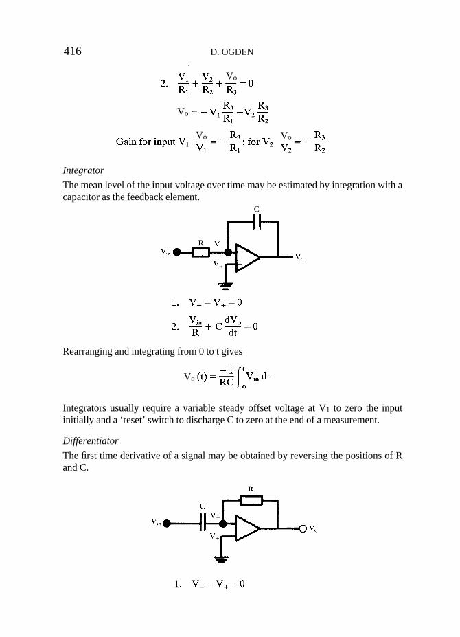
Integrator
The mean level of the input voltage over time may be estimated by integration with acapacitor as the feedback element.
Rearranging and integrating from 0 to t gives
Integrators usually require a variable steady offset voltage at V1 to zero the inputinitially and a ‘reset’ switch to discharge C to zero at the end of a measurement.
Differentiator
The first time derivative of a signal may be obtained by reversing the positions of Rand C.
416 D. OGDEN
Vo
Vo
Vo Vo
Vo
C
R

Non-inverting amplifiers
These are used mainly as buffers from a high resistance voltage scource, e.g. apotentiometer, to provide a low output resistance to drive the subsequent circuitry.The most common gain used is 1, i.e. as a voltage follower
but gains of 10 or more may be used as described above. If good quality operationalamplifiers are used, the voltage follower configuration may be used in microelectrodeamplifiers.
Differential amplifiers
In this case signals are applied at both (+) and (−) inputs and the difference signal V1−V2 is required, sometimes with a gain factor. The following circuit uses a singleoperational amplifier, although for fine tuning of gain and rejection of signalscommon to both V1 and V2 (‘common mode rejection’), a circuit with two or moreamplifiers may be preferable.
417Microelectrode electronics
Vo
Vo
kΩ
Vo
Vo

It can be seen that the gain and common mode rejection (the Vo obtained withV1=V2) of this circuit requires accurately matched values of resistors R1 and ofresistors R2.
Non-ideal characteristics
(1) The open loop gain (A) is high at low frequencies, usually about 105 at 0 Hz, butdeclines markedly as frequency increases, falling to 1 at about 105-107 Hz,depending on the amplifier. The product of gain and bandwidth is a characteristicsometimes specified. Good frequency response can only be obtained at low circuitgain, x, since the condition A/x»1 has to be maintained over a wide frequency range.Gain-bandwidth product is often 100 kHz-1 MHz but may be lower e.g. the‘standard’ 741 has only 10 kHz. It is usually better to realize high gains with 2 ormore sequential amplifiers of low («100) gain if good frequency response isrequired.
(2) Stability. Phase changes occur at high frequencies which may result ininstability due to positive feedback of these frequencies at gains >1. Externalcompensation or a small feedback capacitor may be required to reduce the gain athigh frequencies.
(3) Input resistance and leakage currents. The input impedence and leakagecurrents depend on the type of transistor junction used at the input. Bipolar inputshave 1-2 MΩ impedence and 0.1-10 nA leakage current. The µA741 and NE5534are commonly used bipolar types. Junction field effect transistor (JFET) inputs mayhave 1011-1013 Ω impedence and 1-100 pA leakage current e.g. LF356, BB3523.Other inputs e.g. MOSFET or varactor diode inputs may have 1013-1015 Ωimpedence.
(4) Offset voltage of 0.5-2 mV referred to the input is usually present and canusually be adjusted by an external potentiometer to give zero output.
(5) Noise and drift are usually acceptable but if a critical application is needed,such as a microelectrode input stage, more expensive versions of standard amplifiersselected for low noise and low drift should be used.
Some practical suggestions
It is straightforward and inexpensive to make basic circuits for signal processing,even if some integrated circuits are destroyed in the process. If possible, usepreformed printed circuit boards, e.g. from RSTM, which reduce the possibility ofwiring errors. Always ‘decouple’ each amplifier from interference in the supply linesby 1-10 µF tantalum (NB polarity of tantalum capacitors) and 0.1 µF ceramiccapacitors (for removing high frequency interference) from +15 V and −15 V to thecommon of the power supply. Use a terminating resistor of 50-100 Ω on the output ifa screened cable is used. Make sure that the ground lines to the input and feedbackcircuits of the amplifier do not carry currents to the common of the power supply, or
418 D. OGDEN

other sources of large currents, by use of a parallel earthing pattern to a commonpoint.
5. Current measurement
Current flow in a circuit is measured as the voltage difference across a known valueresistor. In microelectrode experiments the current to ground from the preparationbath is often required. Measurement by the voltage across a resistor e.g. 50 kΩconnected in the ground from the bath is unsatisfactory, mainly because thepotential of the bath then varies with the current and the sensitivity is low (50µV/nA).
A better arrangement is the virtual earth circuit discussed above, which has theadvantage that the bath potential is clamped at a constant level (set by the offsetcircuit), provided currents are not so large that polarization of the bath electrodeoccurs. The sensitivity is now set by the value of RF, VO=−iRF, without affecting thebath potential, and practically may be 1 or 10 mV/nA (RF=1 MΩ or 10 MΩ).
A second use of the virtual ground circuit is to avoid changes of bath potentialresulting from polarization of the ground electrode with large current flow (>1mA). The current is supplied via the feedback arm to a large surface areaplatinum or AgCl electrode and the bath potential monitored with zero currentflow at the inverting input by means of a stable AgCl electrode. It should be notedthat the bath electrodes form part of the feedback circuit and the output VO istherefore influenced by polarization and not useful for current measurementdirectly.
419Microelectrode electronics
kΩ
Current measurement within a circuit is also achieved with an inverting amplifier.A commonly used circuit is
where the second stage is a differential amplifier (A2, resistors omitted) used tosubtract Vin from the output of the current to voltage amplifier A1. This arrangementis used in the patch clamp amplifier and sometimes in the current injection andmonitoring part of voltage clamp circuits.
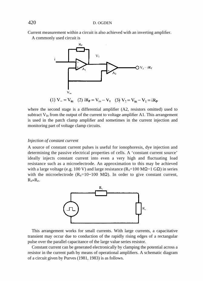
Injection of constant current
A source of constant current pulses is useful for ionophoresis, dye injection anddetermining the passive electrical properties of cells. A ‘constant current source’ideally injects constant current into even a very high and fluctuating loadresistance such as a microelectrode. An approximation to this may be achievedwith a large voltage (e.g. 100 V) and large resistance (Rs=100 MΩ−1 GΩ) in serieswith the microelectrode (Re=10−100 MΩ). In order to give constant current,Rs»Re.
This arrangement works for small currents. With large currents, a capacitativetransient may occur due to conduction of the rapidly rising edges of a rectangularpulse over the parallel capacitance of the large value series resistor.
Constant current can be generated electronically by clamping the potential across aresistor in the current path by means of operational amplifiers. A schematic diagramof a circuit given by Purves (1981, 1983) is as follows.
420 D. OGDEN
V1
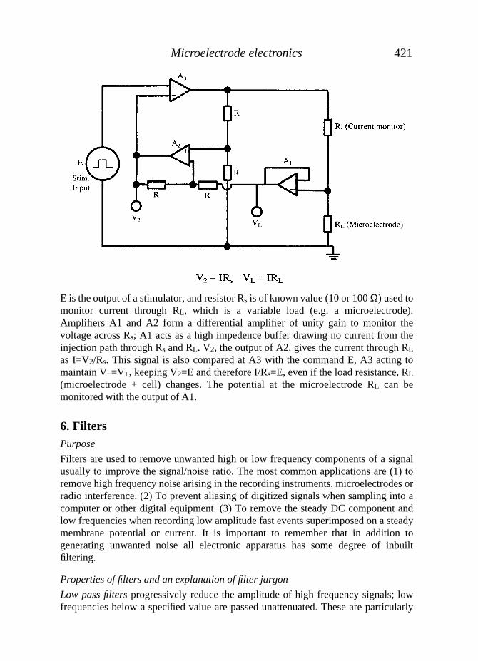
E is the output of a stimulator, and resistor Rs is of known value (10 or 100 Ω) used tomonitor current through RL, which is a variable load (e.g. a microelectrode).Amplifiers A1 and A2 form a differential amplifier of unity gain to monitor thevoltage across Rs; A1 acts as a high impedence buffer drawing no current from theinjection path through Rs and RL. V2, the output of A2, gives the current through RL
as I=V2/Rs. This signal is also compared at A3 with the command E, A3 acting tomaintain V−=V+, keeping V2=E and therefore I/Rs=E, even if the load resistance, RL
(microelectrode + cell) changes. The potential at the microelectrode RL can bemonitored with the output of A1.
6. FiltersPurpose
Filters are used to remove unwanted high or low frequency components of a signalusually to improve the signal/noise ratio. The most common applications are (1) toremove high frequency noise arising in the recording instruments, microelectrodes orradio interference. (2) To prevent aliasing of digitized signals when sampling into acomputer or other digital equipment. (3) To remove the steady DC component andlow frequencies when recording low amplitude fast events superimposed on a steadymembrane potential or current. It is important to remember that in addition togenerating unwanted noise all electronic apparatus has some degree of inbuiltfiltering.
Properties of filters and an explanation of filter jargon
Low pass filtersprogressively reduce the amplitude of high frequency signals; lowfrequencies below a specified value are passed unattenuated. These are particularly
421Microelectrode electronics
useful in removing high frequency instrument noise from relatively low frequencybiological signals.
High pass filtersproduce attentuation of low frequencies below a specified value.Steady signals give zero amplitude output. The a.c. switch on oscilloscope amplifiersproduces high pass filtering below about 1 Hz.
Band pass filtersattenuate frequencies above and below specified values.Filter characteristics are represented (1) in terms of the amplitude response to sine
wave inputs of different frequencies and (2) the time course of the response to a stepinput.
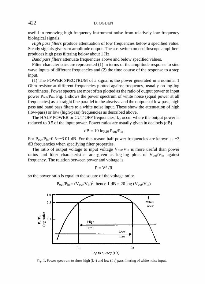
(1) The POWER SPECTRUM of a signal is the power generated in a nominal 1Ohm resistor at different frequencies plotted against frequency, usually on log-logcoordinates. Power spectra are most often plotted as the ratio of output power to inputpower Pout/Pin. Fig. 1 shows the power spectrum of white noise (equal power at allfrequencies) as a straight line parallel to the abscissa and the outputs of low pass, highpass and band pass filters to a white noise input. These show the attenuation of high(low-pass) or low (high-pass) frequencies as described above.
The HALF POWER or CUT OFF frequencies, fc, occur where the output power isreduced to 0.5 of the input power. Power ratios are usually given in decibels (dB)
dB = 10 log10 Pout/Pin
For Pout/Pin=0.5=−3.01 dB. For this reason half power frequencies are known as −3dB frequencies when specifying filter properties.
The ratio of output voltage to input voltage Vout/Vin is more useful than powerratios and filter characteristics are given as log-log plots of Vout/Vin againstfrequency. The relation between power and voltage is
P = V2 /R
so the power ratio is equal to the square of the voltage ratio:
Pout/Pin = (Vout/Vin)2, hence 1 dB = 20 log (Vout/Vin)
422 D. OGDEN
Fig. 1. Power spectrum to show high (fc1) and low (fc2) pass filtering of white noise input.
ForPout/Pin = 0.5 then Vout/Vin = (0.5)0.5 = 0.7
The halfpower frequency, fc, of the voltage ratio therefore occurs at Vout/Vin = 0.7, asshown in Fig. 3.
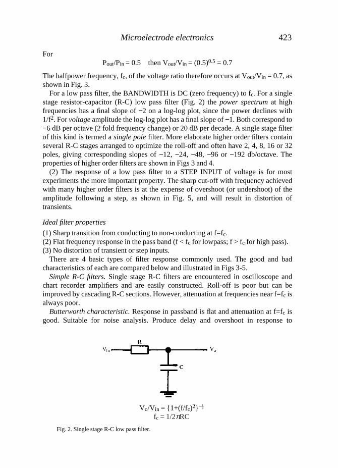
For a low pass filter, the BANDWIDTH is DC (zero frequency) to fc. For a singlestage resistor-capacitor (R-C) low pass filter (Fig. 2) the power spectrumat highfrequencies has a final slope of −2 on a log-log plot, since the power declines with1/f2. For voltageamplitude the log-log plot has a final slope of −1. Both correspond to−6 dB per octave (2 fold frequency change) or 20 dB per decade. A single stage filterof this kind is termed a single polefilter. More elaborate higher order filters containseveral R-C stages arranged to optimize the roll-off and often have 2, 4, 8, 16 or 32poles, giving corresponding slopes of −12, −24, −48, −96 or −192 db/octave. Theproperties of higher order filters are shown in Figs 3 and 4.
(2) The response of a low pass filter to a STEP INPUT of voltage is for mostexperiments the more important property. The sharp cut-off with frequency achievedwith many higher order filters is at the expense of overshoot (or undershoot) of theamplitude following a step, as shown in Fig. 5, and will result in distortion oftransients.
Ideal filter properties
(1) Sharp transition from conducting to non-conducting at f=fc.(2) Flat frequency response in the pass band (f < fc for lowpass; f > fc for high pass).(3) No distortion of transient or step inputs.
There are 4 basic types of filter response commonly used. The good and badcharacteristics of each are compared below and illustrated in Figs 3-5.
Simple R-C filters. Single stage R-C filters are encountered in oscilloscope andchart recorder amplifiers and are easily constructed. Roll-off is poor but can beimproved by cascading R-C sections. However, attenuation at frequencies near f=fc isalways poor.
Butterworth characteristic. Response in passband is flat and attenuation at f=fc isgood. Suitable for noise analysis. Produce delay and overshoot in response to
423Microelectrode electronics
Fig. 2. Single stage R-C low pass filter.
Vo/Vin = 1+(f/f c)2 −G
fc = 1/2πRC

424 D. OGDEN
Fig. 3. Cascade R-C filter sections. (a) In the region near fc on a linear scale. (b) On logcoordinates. n is the number of cascaded sections (poles).
Fig. 4. Comparison of filter characteristics for n=6.
Fig. 5. Response of Butterworth and Bessel low pass filters (n=6) to a step input at t=0.

transient signals, therefore unsuitable for single channel currents, action potentials,synaptic potentials, voltage clamp currents etc.
Bessel characteristic. No delay and minimum overshoot with transient input.Suitable for single channel current etc. signals. Attenuation in region f=fc is poor andtherefore not as good as Butterworth for spectral analysis of noise signals.
Tchebychev characteristic. Good attenuation at f=fc and a steep roll-off. However,the passband contains some degree of ‘ripple’ and transient inputs are distorted. Thistype of response is unsuitable for analysis but may be encountered in some equipmente.g. in FM tape recorders to remove the carrier frequency.
Data sampling and digitization
The main application of high order (4, 8, 16 pole) filters is in sampling a signal priorto digitization by a laboratory interface for computer display or analysis. Duringdigitization the amplitude of the signal is measured at constant intervals determinedby the sampling frequency, and stored as binary numbers.
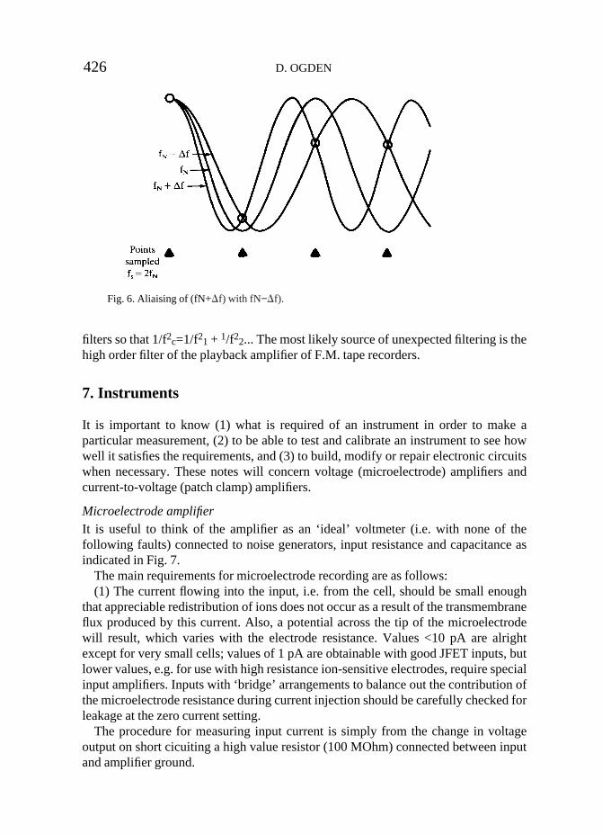
Spectral (noise) analysis. The signal can be regarded as a sum of periodic waves ofdiffering frequencies, phase and amplitude. The highest frequency that can bemeasured will be determined by the sampling frequency. The need to use high orderlow pass filters arises from the possibility of aliasing in the digitized record, i.e. thespurious addition of frequencies higher than 0.5 times the digitizing frequency tofrequencies within the range sampled. If fs is the digitizing frequency and f«0.5fs,then the signal at frequencies of nfs±f (n is an integer) appears added to that at f. Toavoid this, the maximum frequency that can be present in the record withoutproducing aliasing is fN=0.5 fs (the Nyquist frequency) so data are low-pass filtered ator below fN during sampling. An illustration of aliasing is given in Fig. 6, whichshows the periodic wave at the Nyquist frequency sampled twice every cycle, andwaves of frequencies (fN−∆f) lower and (fN+∆f) higher. If both are present in a signalthey are sampled and contribute to the total amplitude. However, their frequencies areindistinguishable at this sampling rate and the sum of their amplitudes would beattributed to (fN−∆f).
Maximum suppression of high frequencies is achieved with a high orderButterworth type response, which is suitable for noise analysis at frequencies up tofc=fN.
Transients.As mentioned above, the Butterworth response is unsuitable fortransient signals. The Bessel response is OK but has poor suppression of frequenciesin the region of the half power frequency. The bandwidth should be selected so as notto distort the rise and fall times of the transients. Generally for a Bessel type the 10-90% risetime for a step input is 0.34/fc. An action potential rises in less than 100 µsand a bandwidth of 5-10 kHz is needed to avoid distortion. Data should be sampled at5-10 times the desired bandwidth to ensure good definition of the time course of thetransient.
Sequential low pass filtering. Data may be filtered more than once before samplingor final display as a result of low pass filters in the several instruments used forrecording, storing and playing back data. The net result is an approximate addition of
425Microelectrode electronics
filters so that 1/f2c=1/f21 + 1/f22... The most likely source of unexpected filtering is thehigh order filter of the playback amplifier of F.M. tape recorders.
7. Instruments
It is important to know (1) what is required of an instrument in order to make aparticular measurement, (2) to be able to test and calibrate an instrument to see howwell it satisfies the requirements, and (3) to build, modify or repair electronic circuitswhen necessary. These notes will concern voltage (microelectrode) amplifiers andcurrent-to-voltage (patch clamp) amplifiers.
Microelectrode amplifierIt is useful to think of the amplifier as an ‘ideal’ voltmeter (i.e. with none of thefollowing faults) connected to noise generators, input resistance and capacitance asindicated in Fig. 7.
The main requirements for microelectrode recording are as follows:(1) The current flowing into the input, i.e. from the cell, should be small enough
that appreciable redistribution of ions does not occur as a result of the transmembraneflux produced by this current. Also, a potential across the tip of the microelectrodewill result, which varies with the electrode resistance. Values <10 pA are alrightexcept for very small cells; values of 1 pA are obtainable with good JFET inputs, butlower values, e.g. for use with high resistance ion-sensitive electrodes, require specialinput amplifiers. Inputs with ‘bridge’ arrangements to balance out the contribution ofthe microelectrode resistance during current injection should be carefully checked forleakage at the zero current setting.
The procedure for measuring input current is simply from the change in voltageoutput on short cicuiting a high value resistor (100 MOhm) connected between inputand amplifier ground.
426 D. OGDEN
Fig. 6. Aliaising of (fN+Df) with fN−Df).
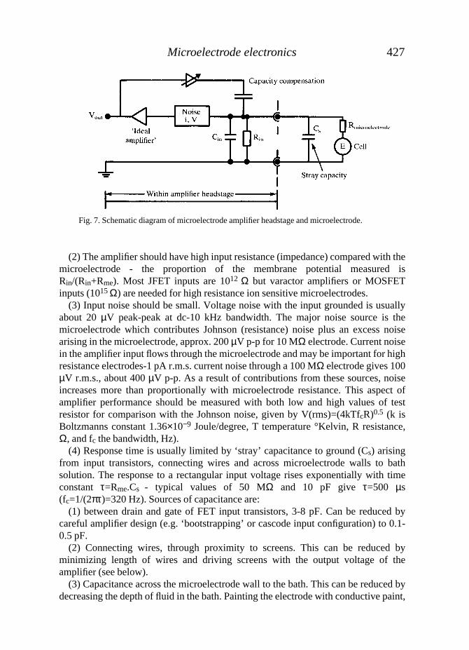
(2) The amplifier should have high input resistance (impedance) compared with themicroelectrode - the proportion of the membrane potential measured isRin/(Rin+Rme). Most JFET inputs are 1012 Ω but varactor amplifiers or MOSFETinputs (1015 Ω) are needed for high resistance ion sensitive microelectrodes.
(3) Input noise should be small. Voltage noise with the input grounded is usuallyabout 20 µV peak-peak at dc-10 kHz bandwidth. The major noise source is themicroelectrode which contributes Johnson (resistance) noise plus an excess noisearising in the microelectrode, approx. 200 µV p-p for 10 MΩ electrode. Current noisein the amplifier input flows through the microelectrode and may be important for highresistance electrodes-1 pA r.m.s. current noise through a 100 MΩ electrode gives 100µV r.m.s., about 400 µV p-p. As a result of contributions from these sources, noiseincreases more than proportionally with microelectrode resistance. This aspect ofamplifier performance should be measured with both low and high values of testresistor for comparison with the Johnson noise, given by V(rms)=(4kTfcR)0.5 (k isBoltzmanns constant 1.36×10⁻⁹ Joule/degree, T temperature °Kelvin, R resistance,Ω, and fc the bandwidth, Hz).
(4) Response time is usually limited by ‘stray’ capacitance to ground (Cs) arisingfrom input transistors, connecting wires and across microelectrode walls to bathsolution. The response to a rectangular input voltage rises exponentially with timeconstant τ=Rme.Cs - typical values of 50 MΩ and 10 pF give τ=500 µs(fc=1/(2πτ)=320 Hz). Sources of capacitance are:
(1) between drain and gate of FET input transistors, 3-8 pF. Can be reduced bycareful amplifier design (e.g. ‘bootstrapping’ or cascode input configuration) to 0.1-0.5 pF.
(2) Connecting wires, through proximity to screens. This can be reduced byminimizing length of wires and driving screens with the output voltage of theamplifier (see below).
(3) Capacitance across the microelectrode wall to the bath. This can be reduced bydecreasing the depth of fluid in the bath. Painting the electrode with conductive paint,
427Microelectrode electronics
Fig. 7. Schematic diagram of microelectrode amplifier headstage and microelectrode.
insulating with varnish and driving the paint screen with the ×1 output is veryeffective. Driven screens of this kind place the same voltage signal on the screen asthat present on the input, thereby removing capacitative coupling between input andscreen for signals of similar waveform, without loss of shielding from unwantedexternal scources. However, current noise applied to the screen from the output willbe transmitted capacitatively into the input and so may make recordings with highresistance electrodes noisier.
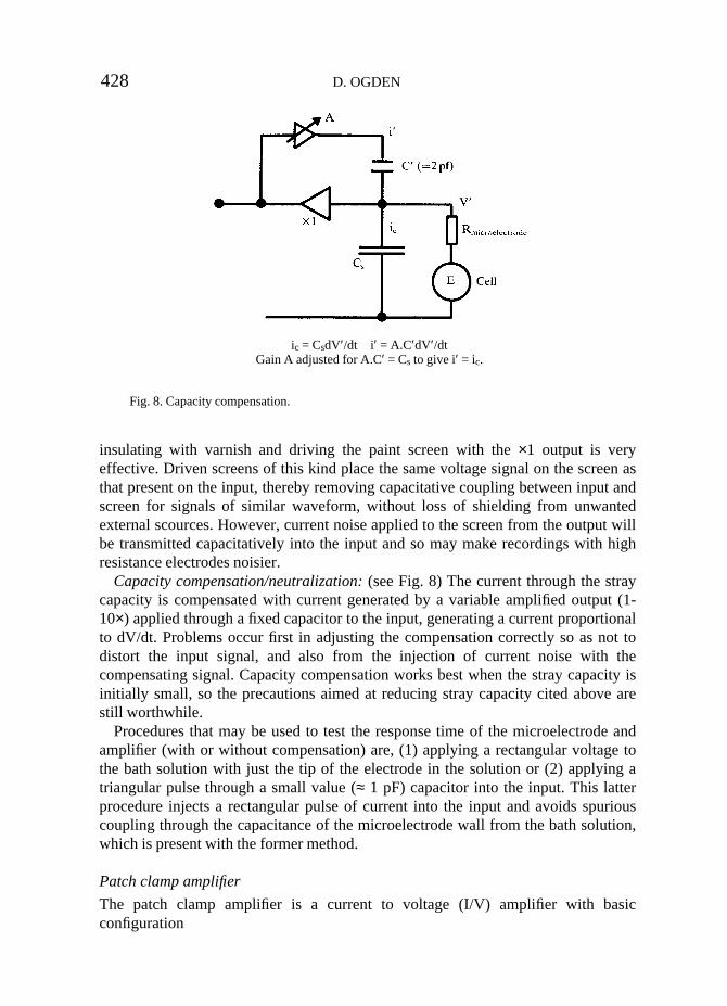
Capacity compensation/neutralization: (see Fig. 8) The current through the straycapacity is compensated with current generated by a variable amplified output (1-10×) applied through a fixed capacitor to the input, generating a current proportionalto dV/dt. Problems occur first in adjusting the compensation correctly so as not todistort the input signal, and also from the injection of current noise with thecompensating signal. Capacity compensation works best when the stray capacity isinitially small, so the precautions aimed at reducing stray capacity cited above arestill worthwhile.
Procedures that may be used to test the response time of the microelectrode andamplifier (with or without compensation) are, (1) applying a rectangular voltage tothe bath solution with just the tip of the electrode in the solution or (2) applying atriangular pulse through a small value (≈ 1 pF) capacitor into the input. This latterprocedure injects a rectangular pulse of current into the input and avoids spuriouscoupling through the capacitance of the microelectrode wall from the bath solution,which is present with the former method.
Patch clamp amplifier
The patch clamp amplifier is a current to voltage (I/V) amplifier with basicconfiguration
428 D. OGDEN
Fig. 8. Capacity compensation.
ic = CsdV′/dt i′ = A.C′dV′/dtGain A adjusted for A.C′ = Cs to give i′ = ic.

where the amplifier A maintains the (−) input at the same potential as (+) i.e. VR, bynegative feedback through resistor Rf. Thus, if the current flowing into (−) isneglected, ip+if=0 and (VO−VR)=ifRf=−ipRf.
Background noise in patch clamp recording depends critically on the impedence ofpipette-cell seal at the input and on the feedback resistance, Rf. It is important toremember that current noise at the input matters in patch clamp recording. Sources ofnoise are (1) the seal and feedback resistances and (2) voltage noise in the amplifier input.
(1) The (−) input is connected to ground via Rs (seal and bath) and Rf (amplifieroutput). The source (seal) resistance Rs and feedback Rf give rise to voltage noise ofapproximately
Vrms = (4kTfcR)G
for ideal resistances, where k is Boltzmanns constant, T temperature (Kelvin) and fc isthe upper frequency limit (bandwidth, i.e. low pass filter setting). The current noise
irms = Vrms/R,so
irms = (4kTfc/R)G
Thus, background current noise due to source and feedback resistances decreases as1/R. Values of Rf of 10-50 GΩ are used for this reason, and good seal resistances (5-50 GΩ) are necessary for low noise recording (see also next section).
(2) Voltage noise arises in the JFET transistors used for the input stage of theamplifier. This is due to (a) ‘shot noise’ of the input current, resulting from movementof discrete charge carriers (b) thermal variations in internal current flow through theJFET seen as input voltage noise when feedback is applied to the input. This voltagenoise gives rise to currents flowing in the stray capacitance of the input. The currentsincrease greatly with recording frequency such that spectral density of input current
429Microelectrode electronics

Si = (2πfC)2.SV
where f is the frequency bandwidth, C the total capacitance and SV the spectraldensity of input voltage noise.
Sources of input capacitance are (1) within the amplifier, mainly across FETjunctions and from input lead to ground, approx. 10-20 pF. (2) Across the holder andpipette to adjacent grounded surfaces e.g. microscope and screens. (3) Across thepipette wall to the bath solution. Use of Sylgard resin or other treatments to coat thepipette exterior reduces capacitance considerably by decreasing creep of fluid alongthe outside of pipette glass and by increasing the thickness of the pipette wall.Minimising the bath level and drying the electrode holder when changing pipettesalso reduces capacitance due to fluid films.
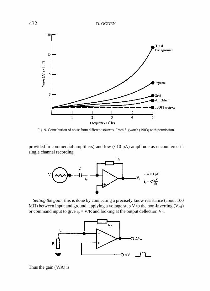
For a good amplifier, a coated pipette and a good seal, the contributions of theelectronics, the pipette and the seal to the total noise are approximately equal, asindicated in Fig. 9.
Frequency response of patch clamp amplifiers.The large values of feedbackresistor used in the patch amplifier result in an output time course, following a suddenor step input current, which is dominated by the parallel stray capacity associatedwith the resistor. The patch clamp thus has a low-pass filter charactaristic, so a 50 GΩresistor with capacity across the terminals of only 0.1 pF gives a response timeconstant of τ=5 ms to a step input. This is too slow.
430 D. OGDEN
Provided parallel capacity is uniformly distributed over the resistor the response isapproximately a single exponential. The output voltage for a step input of current ip is
∆V = ipRf(1 − e−t/τ)
A compensating circuit is employed to correct for this slow response by (a)differentiating the response,
dv −iRf––– = –––– e−t/τdt τ
(b) scaling the differentiated response by τ and adding it to the response itself
V + τdV/dt = −iRf
This procedure is valid for any input waveform and is not affected by pipettecapacitance, providing compensation for Cf independent of recording conditions, andcan give response time constants of 20-50 µs for a step input. A circuit that performsdifferentiation, scaling and addition which is often used for compensation is
This operates as a voltage follower at low frequencies but increases in gain at highfrequencies. Time constant R1C is adjusted to the same value as that produced bystray feedback capacitance in the I/V amplifier; R2 provides damping to preventoscillation. If the patch clamp input stage amplifier has a more complicated response,as is the case with commercial switchable resistor designs, then additional waveformshaping circuits are used to compensate the response.
Setting up the compensation: this is most easily done with a square wave currentinjected into the input, adjusting R, (either a panel mounted or internal potentiometer)to give a square output, flat topped up to ~10 ms. A square input current is achievedby capacitively coupling a good triangular voltage waveform to the input, simply byclamping the open end of a screened cable in the vicinity of the input pin. The morecomplicated commercial patch clamps may require adjustments of 4 or moretrimpots. The response should be checked with both high amplitude signals (often
431Microelectrode electronics
Set
provided in commercial amplifiers) and low (<10 pA) amplitude as encountered insingle channel recording.
Setting the gain: this is done by connecting a precisely know resistance (about 100MΩ) between input and ground, applying a voltage step V to the non-inverting (Vref)or command input to give ip = V/R and looking at the output deflection Vo:
Thus the gain (V/A) is
432 D. OGDEN
Fig. 9. Contribution of noise from different sources. From Sigworth (1983) with permission.
∆VoR∆Vo/ip = –––––––∆V
The gain is adjusted to give convenient units of Vo/ip e.g. 10 mV/pA by an internalpotentiometer at a later stage of amplification.
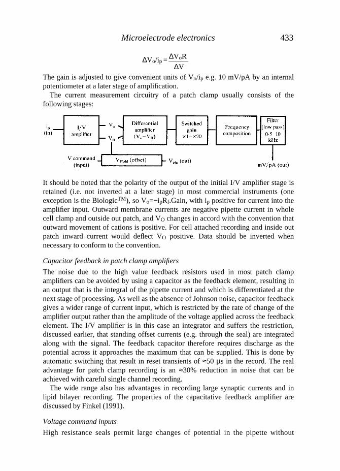
The current measurement circuitry of a patch clamp usually consists of thefollowing stages:
It should be noted that the polarity of the output of the initial I/V amplifier stage isretained (i.e. not inverted at a later stage) in most commercial instruments (oneexception is the BiologicTM), so Vo=−ipRf.Gain, with ip positive for current into theamplifier input. Outward membrane currents are negative pipette current in wholecell clamp and outside out patch, and VO changes in accord with the convention thatoutward movement of cations is positive. For cell attached recording and inside outpatch inward current would deflect VO positive. Data should be inverted whennecessary to conform to the convention.
Capacitor feedback in patch clamp amplifiers
The noise due to the high value feedback resistors used in most patch clampamplifiers can be avoided by using a capacitor as the feedback element, resulting inan output that is the integral of the pipette current and which is differentiated at thenext stage of processing. As well as the absence of Johnson noise, capacitor feedbackgives a wider range of current input, which is restricted by the rate of change of theamplifier output rather than the amplitude of the voltage applied across the feedbackelement. The I/V amplifier is in this case an integrator and suffers the restriction,discussed earlier, that standing offset currents (e.g. through the seal) are integratedalong with the signal. The feedback capacitor therefore requires discharge as thepotential across it approaches the maximum that can be supplied. This is done byautomatic switching that result in reset transients of ≈50 µs in the record. The realadvantage for patch clamp recording is an ≈30% reduction in noise that can beachieved with careful single channel recording.
The wide range also has advantages in recording large synaptic currents and inlipid bilayer recording. The properties of the capacitative feedback amplifier arediscussed by Finkel (1991).
Voltage command inputs
High resistance seals permit large changes of potential in the pipette without
433Microelectrode electronics
large current flow across the seal into the pipette from the bath. In response to avoltage step applied to Vref, the I/V amplifier produces an output such that currentflow through Rf causes the same potential change in the pipette. In order toimprove the signal to noise, so as to reduce the contribution of noise on thecommand, these are divided by a factor, often 10, in the I/V amplifier i.e. Vref=0.1VCommand.
The current flowing into the pipette is the sum of currents (a) through themembrane patch (e.g. single channel currents), (b) through the seal resistance and (c)to charge the input capacity of the amplifier and pipette; (a) is the quantity measured,(b) produces a small, relatively constant offset with good seals, (c) produces largetransients in response to rapid potential changes (i=CdV/dt) and may lead tosaturation of the I/V amplifier or frequency compensation circuit. These transientsobscure single channel currents following a voltage step, and if saturation of theamplifier occurs, may result in loss of voltage control in the pipette and, because ofthe long recovery times of amplifiers in the circuit, loss of data for several msfollowing a step.
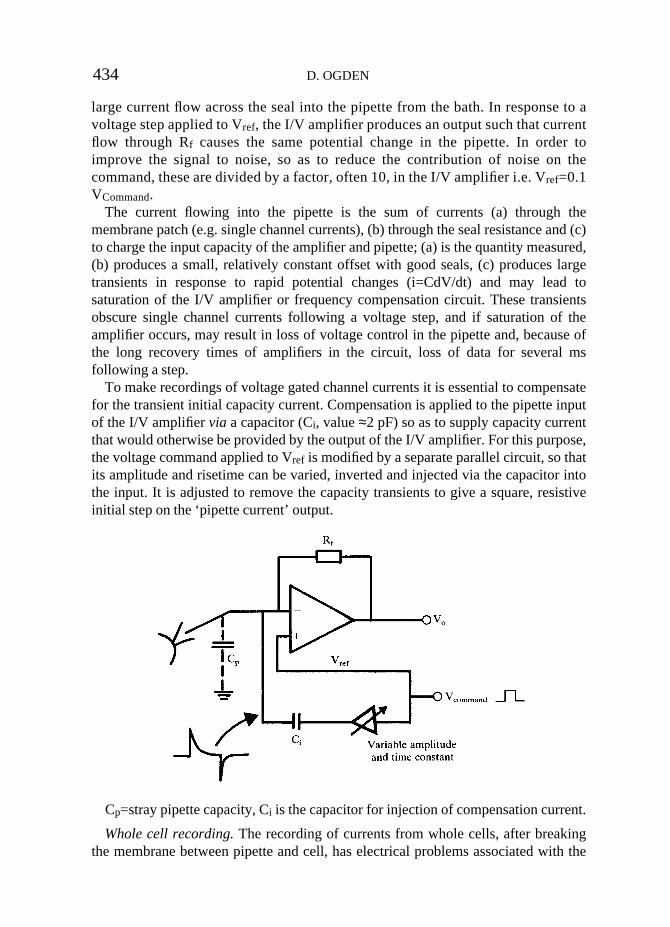
To make recordings of voltage gated channel currents it is essential to compensatefor the transient initial capacity current. Compensation is applied to the pipette inputof the I/V amplifier via a capacitor (Ci, value ≈2 pF) so as to supply capacity currentthat would otherwise be provided by the output of the I/V amplifier. For this purpose,the voltage command applied to Vref is modified by a separate parallel circuit, so thatits amplitude and risetime can be varied, inverted and injected via the capacitor intothe input. It is adjusted to remove the capacity transients to give a square, resistiveinitial step on the ‘pipette current’ output.
Cp=stray pipette capacity, Ci is the capacitor for injection of compensation current.
Whole cell recording. The recording of currents from whole cells, after breakingthe membrane between pipette and cell, has electrical problems associated with the
434 D. OGDEN

extra cell capacity to be charged through the series resistance of the pipette/celljunction:
Voltage pulses to Vref (and hence the pipette) cause current to flow into the cellthrough Rs to charge the cell capacitance, Cm. This gives rise to a current output withinitial transients of time constant
and an initial amplitude V/Rs. Thus, after compensation for fast transients, thesemuch slower transients may be used to calculate Rs and Cm. The capacity currentrequired to charge Cm may be compensated in the same way as for the pipettecapacitance, i.e. by applying a current of variable magnitude and risetime to the inputby injection through the capacitor Ci. This slow capacitance compensation isgenerated in parallel with the fast compensation and added to the signal injectedthrough Ci. Calibration of the compensation circuit allows Cm and Rs to be read fromdials on front panel calibrated potentiometers.
Unlike a microelectrode amplifier, the use of slow capacitance compensation doesnot improve the speed of clamping the cell membrane potential (unless the amplifiershave reached saturation) but simply removes the capacitative transient from the
435Microelectrode electronics
‘Cslow’, τslow
‘Cfast’, τfast
»
pipette current and amplifier output. The limiting frequency characteristics of theresponse of the cell for noise analysis or to a potential step has τ≈RsCm as before.
The presence of the series resistance Rs gives rise to an error voltage between theclamped pipette potential and the true value of the cell membrane potential,
Vc − Vp = ipRs.
Thus, it is important to know the value of Rs so that corrections can be applied tocurrent/voltage data for the error of Vc. Also, as mentioned above, the transientresponse of the system is attenuated by the RsCm time constant, which for cells of e.g.10-20 pF and Rs of 10-20 MΩ may produce low pass filtering at around 400 Hz.
The effect of Rs is to underestimate Vc by an amount proportional to the recordedcurrent. Compensation for this effect (‘series resistance compensation’) may be madeby feeding back a proportion of the current signal to Vref. In commercial amplifiersthe value of series resistance is taken from the whole cell transient cancellation,multiplied by ip and a proportion, up to about 80%, and added to Vref. However, thisoften results in instability and some adjustment to the phase of the compensation maybe present. In practice the value of Rs often increases or fluctuates on a minute orshorter timescale during recording, often making series resistance compensationimprecise. As with other cases where compensation is applied, the best results areobtained with a low initial series resistance.
8. Grounding and screening
Ground lines or earths serve four distinct functions in electrophysiologicalequipment. These are:
(1) Safety. All instrument cases and other enclosures of apparatus with a mainssupply must have a reliable connection to the mains earth through the plug.
(2) Reference potential. Provide the reference (zero) potential for measurements ofcell potentials and also for each stage of signal processing that occurs withininstruments. Any unwanted signal present on the reference ground of an amplifierwill appear in the output and be passed on to the next stage. The reference point is thesignal ground of the input amplifier or oscilloscope input. Leads connecting the signalground should carry no current and run next to or twisted with the signal from theinput amplifier, to reduce the area of loop susceptible to magnetic interference.
(3) Current returns. To return current to the common of power supplies from e.g.zener diodes, relays, lamps, decoupling circuits. These common returns should be runseparately from reference grounds to a central grounding point.
(4) Screening.Electrostatic screening to prevent interference from mainly 50 (or60) Hz is achieved with a Faraday cage and by ensuring that all conductingmechanical parts such as microscope objective, condenser and stage, the baseplateand micromanipulators have good, low resistance («1 Ω) connections to ground. Thecloser a component is to the pipette, the more important a good connection.
Magnetic interferencefrom transformers or motors occurs by induction in circuit
436 D. OGDEN
loops of large area oriented across the magnetic field generated. This form ofinterference is often of 100 or 150 Hz and can be prevented by re-routing ground linesto minimize the area presented to the field, or by moving the source of theinterference.
It is usual to arrange grounding to a central point, often on the oscilloscope input,running separate lines for reference and screens to equipment in the cage or rack.Current returns go to the common of the power supply first, which is in turnconnected by a single wire to the central ground point. The central point can be takento the mains earth via the oscilloscope cable or by a separate lead.
9. Test equipment
Testing can mostly be done with electrophysiological apparatus already present i.e.an oscilloscope, a precisely timed square wave or pulse generator, such as aDigitimer, and an accurate voltage source or calibrator. Digital multimeters (orDMM) provide accurate measurement of steady potential, current and resistance. Agood signal generator or other equipment for occasional use can often be shared orborrowed.
Electronics reading list
CLAYTON, G. B. (1979). Operational Amplifiers. 2nd Edition, London: Butterworths.HOROWITZ, P. & HILL, W. (1989). The Art of Electronics. 2nd Edition, Cambridge: C.U.P.PURVES, R. D. (1981). Microelectrode Methods for Intracellular Recording and Iontophoresis.
London, New York: Academic Press.FINKEL, A. S. (1991). Progress in instrumentation technology for recording from single channels and
small cells. In Molecular Neurobiology(ed. Chad, J. & Wheal, H.V.). Oxford: IRL Press.
Specialist articles
MARSHALL, M. A. (1976). Earthing, Shielding and Filtering Problems. 4 articles in Wireless World,August, September, November and December, 1976.
PURVES, R. D. (1983). High impedence electronics. 2 articles in Wireless World, March, April, 1983.SIGWORTH, F. J. (1983). Electronic design of the patch clamp: In Single Channel Recording. (ed.
Sakmann & Neher). N.Y.: Plenum.WILLIAMS, T. (1991). The Circuit Designer Companion.Butterworth-Heinemann. (Good chapter on
earthing and shielding.)
Applications manuals from:Siliconix (FETs), National Semiconductor (FETs and 0p Amps), BurrBrown (0p Amps).
437Microelectrode electronics


![[tel-00861119, v1] Implantable microelectrode biosensors for - HAL](https://img.pdfslide.net/doc/110x75/620615a58c2f7b17300473ad/tel-00861119-v1-implantable-microelectrode-biosensors-for-hal.jpg)