Embed Size (px)
Citation preview
THE 1149.6 TEST RECIVER
Presentation In The Framework Of JTAG Course
Lior Vaknin - June 2005

Introduction
Alternative connection methodologies for propagating signals between modules.

The distances signal travels may be short, for example, a few centimeters on boards but could range up to several meters in systems.

A signal is defined as having a source or transmitter and adestination, or receiver and travels along a path, typically a wire.

Examples for Designing Path FactorsThe speed of signal propagation is the speed of light: =>data rates become high, propagation speed interact with the distance the signal must travel.
Signal can be damaged, encoded information is degraded or lost: =>unwanted noise is added into the information signal.
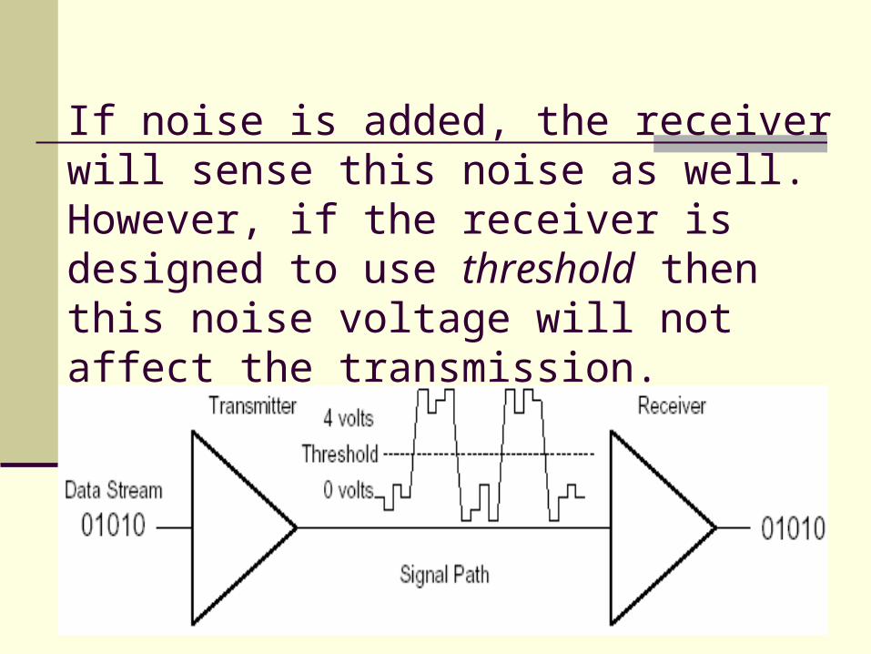
If noise is added, the receiver will sense this noise as well. However, if the receiver is designed to use threshold then this noise voltage will not affect the transmission.

A signal contains power which is to say it takes energy to transmit information. This power is a necessary feature, but can lead to problems, namely heat.

Power can be limited by slowing down the rate of information transfer, or by limiting the voltage swing of the signal.
However this is fraught with risk, since as voltage swings become smaller, the noise immunity offered by signal thresholding is lowered as well.

Signal can reflect off the end of the wire and bounce backward. and adds into the subsequent data waveforms, which is just like adding in noise. This phenomenon can be canceled out by impedance matching

One approach to reducing sensitivity to noise is to have two thresholds.However, there is some time uncertainty about when the receiver will perceive the transition.

AC Coupling

AC coupling is usually performed by adding a capacitor to the path.This capacitor is called a DC blocking capacitor. The combination of a series capacitor and resistor forms a high-pass filter.
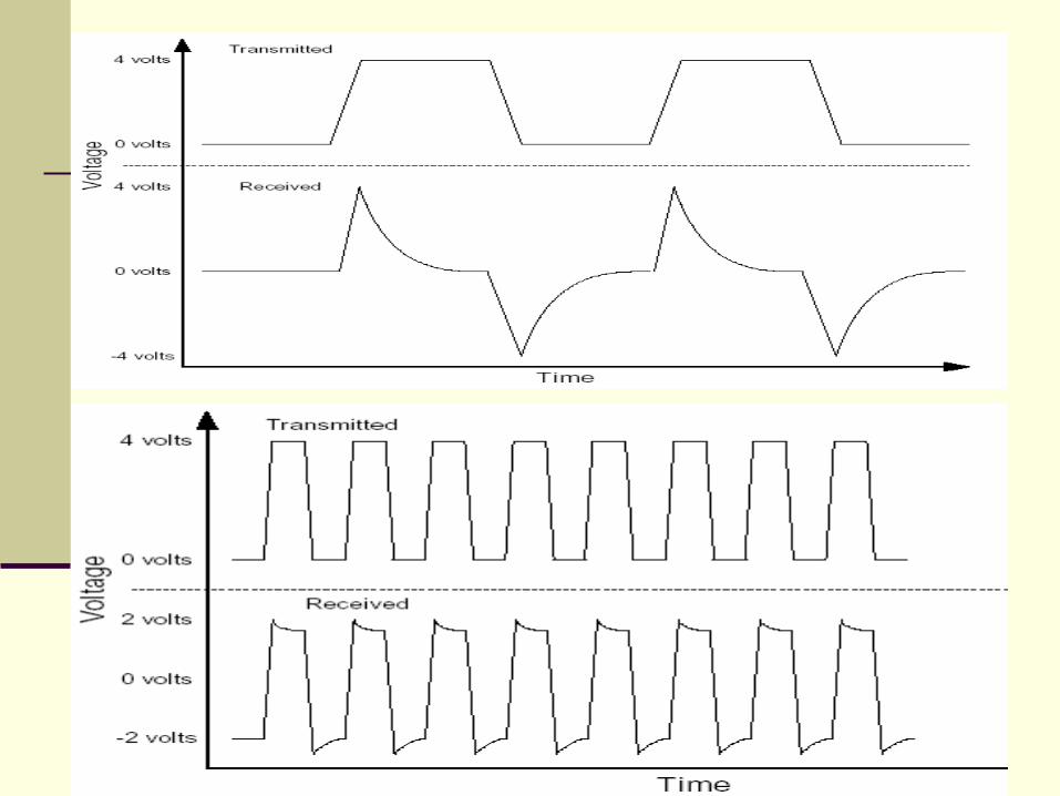

This was steady-state response. But, if the waveform was recently ‘turned on’, there is a time where the voltage is not centered at 0, but effectively centered at 2 volts. This is the transient response.

Designers try to avoid this problem by sending extra bits in the stream that compensate for imbalances in the data. These bits are located in known positions and are later ignored (preload).

Differential Signaling

Use two wires to transmit the same data stream. One wire is the positive and the other is the negative.
The receiver compares the two signals, if Vpos > Vneg producing 1 else producing 0.

How does differential signaling helps ?
First, With mutual references, the forbidden zone is greatly reduced. (much more assurance when transition will be perceived).Second, we can reduce the actual voltage swing, the signal can change faster,better slew rate.

Transition has less ‘distance’ to travel in the same period of time.Thus we can achieve higher data rates with the same edge.
This reduces power and increases the number of edges we can pack into a time period – and increases the data rate.
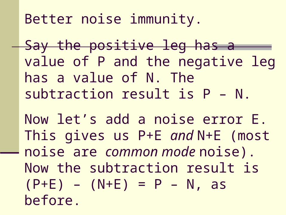
Better noise immunity.
Say the positive leg has a value of P and the negative leg has a value of N. The subtraction result is P – N.
Now let’s add a noise error E. This gives us P+E and N+E (most noise are common mode noise).Now the subtraction result is(P+E) – (N+E) = P – N, as before.

Differential signaling does have costs.
As design requirements for data streams with gigabit capacities become commonplace, we find this also complicates the design. As aresult, each IC vendor confronts these challenges, they may come up with somewhat different solutions. This can lead to ‘single-source’ problems.

AC coupling, as shown here, can help with these problems.(Incompatible when DC coupled)
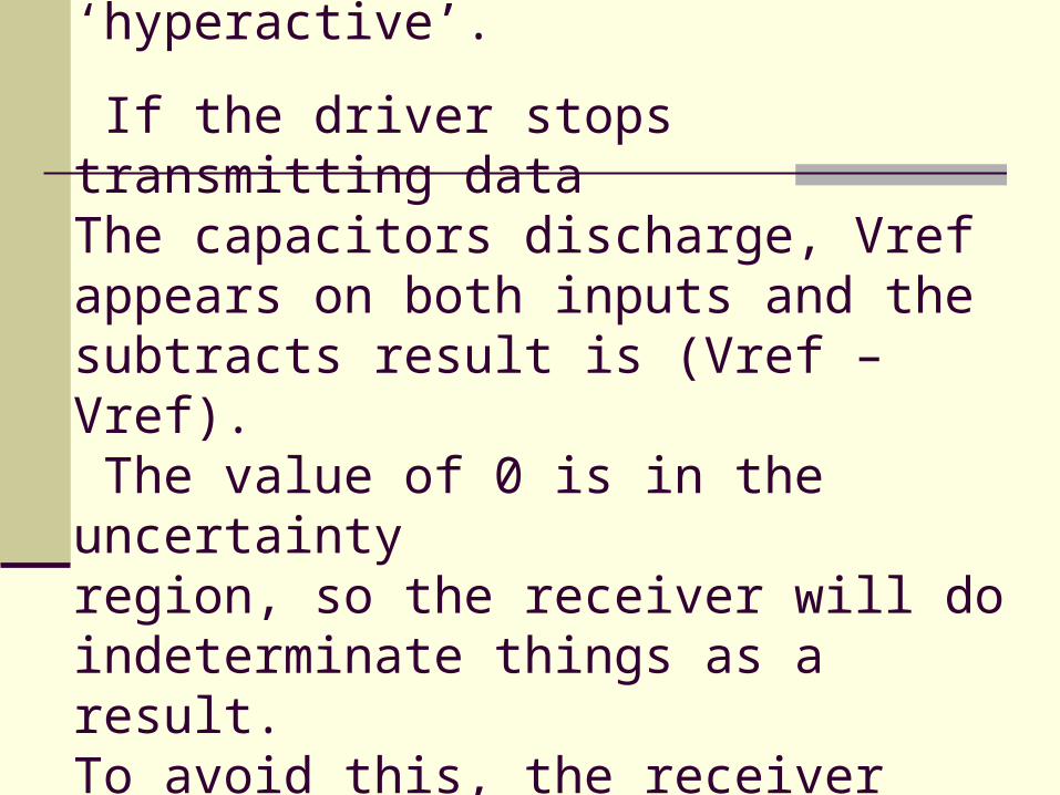
This configuration is also ‘hyperactive’.
If the driver stops transmitting dataThe capacitors discharge, Vref appears on both inputs and the subtracts result is (Vref – Vref). The value of 0 is in the uncertaintyregion, so the receiver will do indeterminate things as a result. To avoid this, the receiver always need some sort of signal (even with ‘idle’)
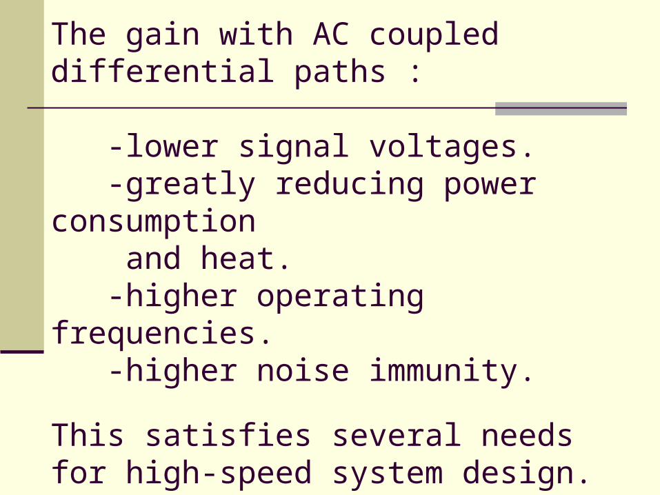
The gain with AC coupled differential paths :
-lower signal voltages. -greatly reducing power consumption and heat. -higher operating frequencies. -higher noise immunity.
This satisfies several needs for high-speed system design.
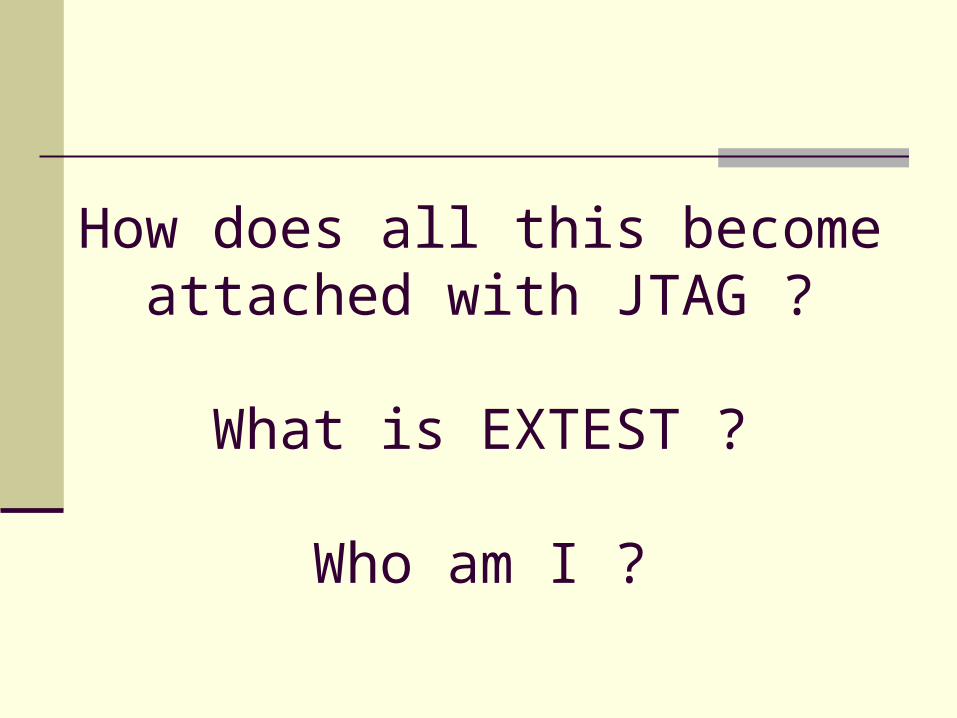
How does all this become attached with JTAG ?
What is EXTEST ?
Who am I ?

THE TEST RECIEVER

Building Blocks
Voltage Comparator Time Hysteresis Memory Reference System - Switchable

DC/AC-Coupled Transition


DC Response

When EXTEST instruction is in effect, the receiver is expected to respond to the voltage levels seen at the input.


AC Response

When the EXTEST_PLUSE or EXTEST_TRAIN instruction are in effect, the test receiver is expected to response to valid signal transitions seen at the input.


An Integrated AC/DC Receiver

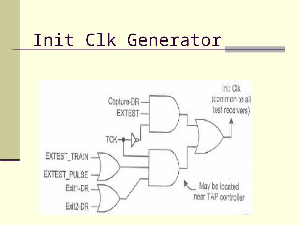
Init Clk Generator

Test Receiver Memory Initialization

THANK YOU !
![Nagra3 Hacked! « Satelly Blog · PDF fileNagra3 Hacked! « Satelly Blog 08/08/2010 22.24.33] deci nu exista alt reciver care poate decoda](https://img.pdfslide.net/doc/110x75/5a9e23547f8b9a39338d8132/nagra3-hacked-satelly-blog-hacked-satelly-blog-08082010-222433-deci-nu-exista.jpg)
![arXiv:1912.05677v1 [physics.soc-ph] 11 Dec 2019 · 2019. 12. 19. · Dana Vaknin, 1Bnaya Gross, Sergey V.Buldyrev,2 and Shlomo Havlin 1Bar-Ilan University, Ramat Gan, Israel 2Yeshiva](https://img.pdfslide.net/doc/110x75/611fdf65ddbe6f45fa3aec94/arxiv191205677v1-11-dec-2019-2019-12-19-dana-vaknin-1bnaya-gross-sergey.jpg)