Embed Size (px)
Citation preview
C A R B O N 6 9 ( 2 0 1 4 ) 4 6 – 5 4
.sc iencedi rect .com
Avai lab le at wwwScienceDirect
journal homepage: www.elsev ier .com/ locate /carbon
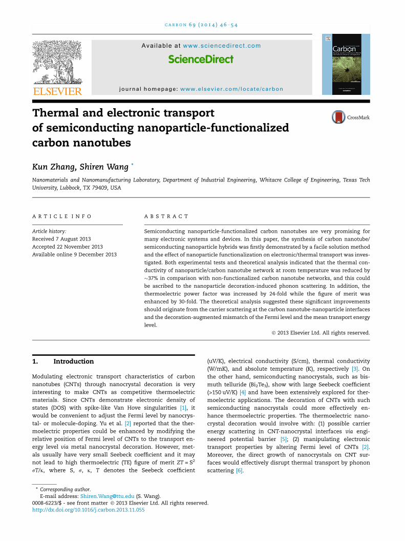
Thermal and electronic transportof semiconducting nanoparticle-functionalizedcarbon nanotubes
0008-6223/$ - see front matter � 2013 Elsevier Ltd. All rights reserved.http://dx.doi.org/10.1016/j.carbon.2013.11.055
* Corresponding author.E-mail address: [email protected] (S. Wang).
Kun Zhang, Shiren Wang *
Nanomaterials and Nanomanufacturing Laboratory, Department of Industrial Engineering, Whitacre College of Engineering, Texas Tech
University, Lubbock, TX 79409, USA
A R T I C L E I N F O
Article history:
Received 7 August 2013
Accepted 22 November 2013
Available online 9 December 2013
A B S T R A C T
Semiconducting nanoparticle-functionalized carbon nanotubes are very promising for
many electronic systems and devices. In this paper, the synthesis of carbon nanotube/
semiconducting nanoparticle hybrids was firstly demonstrated by a facile solution method
and the effect of nanoparticle functionalization on electronic/thermal transport was inves-
tigated. Both experimental tests and theoretical analysis indicated that the thermal con-
ductivity of nanoparticle/carbon nanotube network at room temperature was reduced by
�37% in comparison with non-functionalized carbon nanotube networks, and this could
be ascribed to the nanoparticle decoration-induced phonon scattering. In addition, the
thermoelectric power factor was increased by 24-fold while the figure of merit was
enhanced by 30-fold. The theoretical analysis suggested these significant improvements
should originate from the carrier scattering at the carbon nanotube-nanoparticle interfaces
and the decoration-augmented mismatch of the Fermi level and the mean transport energy
level.
� 2013 Elsevier Ltd. All rights reserved.
1. Introduction
Modulating electronic transport characteristics of carbon
nanotubes (CNTs) through nanocrystal decoration is very
interesting to make CNTs as competitive thermoelectric
materials. Since CNTs demonstrate electronic density of
states (DOS) with spike-like Van Hove singularities [1], it
would be convenient to adjust the Fermi level by nanocrys-
tal- or molecule-doping. Yu et al. [2] reported that the ther-
moelectric properties could be enhanced by modifying the
relative position of Fermi level of CNTs to the transport en-
ergy level via metal nanocrystal decoration. However, met-
als usually have very small Seebeck coefficient and it may
not lead to high thermoelectric (TE) figure of merit ZT = S2
rT/r, where S, r, r, T denotes the Seebeck coefficient
(uV/K), electrical conductivity (S/cm), thermal conductivity
(W/mK), and absolute temperature (K), respectively [3]. On
the other hand, semiconducting nanocrystals, such as bis-
muth telluride (Bi2Te3), show with large Seebeck coefficient
(>150 uV/K) [4] and have been extensively explored for ther-
moelectric applications. The decoration of CNTs with such
semiconducting nanocrystals could more effectively en-
hance thermoelectric properties. The thermoelectric nano-
crystal decoration would involve with: (1) possible carrier
energy scattering in CNT-nanocrystal interfaces via engi-
neered potential barrier [5]; (2) manipulating electronic
transport properties by altering Fermi level of CNTs [2].
Moreover, the direct growth of nanocrystals on CNT sur-
faces would effectively disrupt thermal transport by phonon
scattering [6].
C A R B O N 6 9 ( 2 0 1 4 ) 4 6 – 5 4 47
Many efforts have been made to synthesize inorganic
nanocrystal-decorated CNTs [7–11]. The strategies include ex
situ approaches by attaching the synthesized nanocrystals
onto the CNT surface, and in situ approaches by directly form-
ing nanocrystals on the CNT surface. There have been numer-
ous reports related to CNT supported nanocrystals, such as
CNT/metals (CNT/Au [12], CNT/Pt [13]), CNT/metal oxides
(CNT/TiO2 [14], CNT/MnO2 [15], CNT/SnO2 [16]), and other
CNT/semiconductors (CNT/CdSe [17], CNT/CdTe [18]). For in
situ synthesis of nanocrystals onto CNT surfaces, many meth-
ods have been developed. Unitary inorganic nanoparticles
were deposited on CNTs via sputtering, evaporation or ther-
mal deposition [19–21]. Chemical vapor deposition (CVD)
was also attempted under the oxygen-free environment at
very high temperature [22]. However, those methods are lim-
ited to the binary oxygen-free nanoparticle decoration. CdTe
quantum dots have been attached to the CNT surface by
Banerjee and wong [18] at high temperature (250 �C). Zhou
et al. [23] attached Bi2Te3 nanocrystals onto CNT surface by
microwave-polyol method at 170 �C. The procedure is compli-
cated and high energy-consumption. The resultant Bi2Te3
nanocrystals on CNT surface were irregular and showed wide
size distribution. To the best of our knowledge, no effort has
been made for in situ growth of Bi2Te3 nanocrystals onto
CNT surface at a lower temperature and there is also a lack
of fundamental understanding of how semiconducting nano-
crytals could modulate electronic and thermal transport of
the decorated CNTs.
Herein, we report in situ synthesis of Bi2Te3 nanocrystals
on the surface of multi-walled carbon nanotubes (MWCNTs)
by a facile solution chemical method at a low temperature
for the first time. The morphology of nanocrystals decorated
on MWCNT surface was investigated, and the organic/inor-
ganic interfacial contribution to the thermoelectric properties
was revealed.
2. Experimental section
2.1. Acid treatment of MWCNTs
95% purity MWCNTs (C150-P) with outer mean diameter
�13 nm were purchased from Bayer Material Science AG.
50 mg MWCNTs were added into 150 ml 6 M nitric acid in a
two-necked, round-bottomed glass flask, and refluxed at
120 �C for 5.5 h After refluxing, the mixture was cooled down
to room temperature, washed with copious amount of deion-
ized water, and filtrated using 0.2-micron Nylon filter paper
(Millipore Inc.). Finally, acid-treated MWCNTs were dried in
a vacuum oven at 80 �C overnight.
2.2. Synthesis of Bi2Te3-decorated MWCNTnanostructures
All chemicals were purchased from Sigma–Aldrich and used
without any further purification. In a typical synthesis,
6.06 g bis(2-ethylhexyl) sulfosuccinate (AOT) was dissolved
in 40 ml isooctane. Then, 37 mg telluric acid (Te(OH)6) was
dissolved in 0.6 ml deionized water. Another solution was
also prepared by addition of 33.5 mg bismuth chloride (BiCl3)
into the 0.4 ml nitric acid. Subsequently, 20 ml AOT/isooctane
was added into each solution. Next, 0.06 ml thioglycolic acid
(TGA) was introduced into the BiCl3/AOT/isooctane mixture.
Both solutions were then sonicated for 15 min to form uni-
form solutions. Afterwards, 50 mg acid-treated MWCNTs
were added into BiCl3/AOT/isooctane solution followed with
subsequent bath sonication for 1.5 h Then two solutions were
mixed and subjected to ultrasonic processing for 1 h. Subse-
quently, 1.5 g hydrazine monohydrate (64–65 wt.%) was added
into the mixture with vigorous stirring at room temperature
overnight. The resultant precipitates were collected by filtra-
tion through the 0.2-micron Nylon filter membrane, and the
solid samples were extensively washed with isooctane, etha-
nol and copious amounts of deionized water in sequence to
remove any impurity residuals, including thioglycolic acid
on Bi2Te3 nanocrystals, and AOT etc. Other samples were also
prepared at the same procedure with different AOT concen-
trations (0.341 M and 0.085 M).
2.3. Structure characterization of Bi2Te3-decoratedMWCNT nanostructures
Bi2Te3-decorated MWCNTs nanostructures were character-
ized by transmission electron microscopy (TEM, Hitachi
H-8100) and high-resolution TEM (HRTEM, JEM 2100). The
Bi2Te3-decorated MWCNT nanostructures dispersed and son-
icated in toluene were drop-casted onto an ultrathin holey
carbon-coated copper grid, and dried prior to electron micros-
copy. Energy-dispersive spectroscopy (EDS) was used to quan-
tify atomic ratios. As-received MWCNTs and acid-treated
MWCNTs were also characterized by Raman spectroscopy
(Senterra Raman microscopy, Bruker Inc.) using a 532 nm la-
ser. The samples were also characterized by Powder X-ray Dif-
fraction (PXRD) with a Rigaku Ultima III diffractometer using
Cu Ka. To prepare the samples for powder X-ray diffraction,
the sample was finely grounded. The measurements were ta-
ken at a 2h range of 20–60� at a step-width of 0.03 sec�1. Pow-
der XRD patterns were analyzed by referring to the
International center: for Diffraction Data (ICDD) powder dif-
fraction file (PDF) database. Size distributions for Bi2Te3 nano-
crystals on MWCNTs were analyzed in commercial software,
ImageJ.
2.4. Thermal/electrical characterization
Thermal conductivities were measured by Nanoflash thermal
analysis equipment (LFA 447, NETZSCH Instruments). For the
Seebeck coefficient measurement, the Seebeck voltage was
collected by connecting Keithley 2182A Nanvoltmeter with
two identical bare copper wires, which were bonded onto pel-
lets at 10 mm spacing by silver paste. The temperature gradi-
ent was obtained using two K-type thermocouples (Omega
Inc.), controlled by SM325 thermometer data logger). The See-
beck coefficient measurement was calibrated before mea-
surement, and the Seebeck coefficient was calculated with
S = �DV/DT + SCu, where SCu is 6.5 uV/K at room temperature
[24]. Electrical conductivity was measured using a SRM probe
(Bridge Technology Inc.) by a standard four-point probe meth-
od with a Keitley 2400 current source meter and a Keitley
2182A nanovolt meter at the room temperature. Acid-treated
48 C A R B O N 6 9 ( 2 0 1 4 ) 4 6 – 5 4
MWCNTs were used as the control sample for the investiga-
tion of thermoelectric properties.
3. Results and discussion
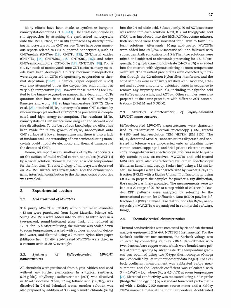
The in situ synthesis of Bi2Te3 nanocrystals on MWCNT sur-
face is illustrated in Fig. 1. It involves several steps, including
the formation of reverse micelles, ion adsorption and reduc-
tion. Due to the amphiphilic characteristics of AOT mole-
cules, AOT encapsulated aqueous droplets in the isooctane
solution, resulting in reverse micelles. Subsequently, the re-
verse micelles were anchored on the MWCNT surface due to
the hydrophobic interaction [25–27]. In theory, hydrophobic
chains of AOT surfactants interact with the sidewall of
MWCNTs through hydrophobic interaction, thereby anchor-
ing AOT surfactant molecules to MWCNTs and leaving hydro-
philic head groups facing the aqueous phase inside the AOT
reverse micelles. As a result, acid-treated MWCNTs stay inti-
mate contact with micelles. BiCl3 and Te(OH)6 were dissolved
in aqueous droplets and thus confined in the AOT reverse mi-
celles. The micelles containing Bi3+ were firstly adsorbed on
acid-treated MWCNT surface. Subsequently, added micelles
containing Te(OH)6 were then mixed and merged with the mi-
celles containing Bi3+ forming microemulsions with Bi and Te
ions on MWCNT surfaces. Bi2Te3 nancrystals were synthe-
Fig. 1 – Schematic illustration of in situ synthesis of Bi2Te3 on M
adsorption and reduction on the MWCNT surfaces. (A color ver
sized with reduction by hydrazine mononhydrate in mixed
microemulsions.
Since the AOT concentration may affect the micelle size
and thus the nanocrystal morphology on MWCNT surface,
different AOT concentrations were used to understand the ef-
fect of AOT concentration on Bi2Te3/MWCNT hybrid struc-
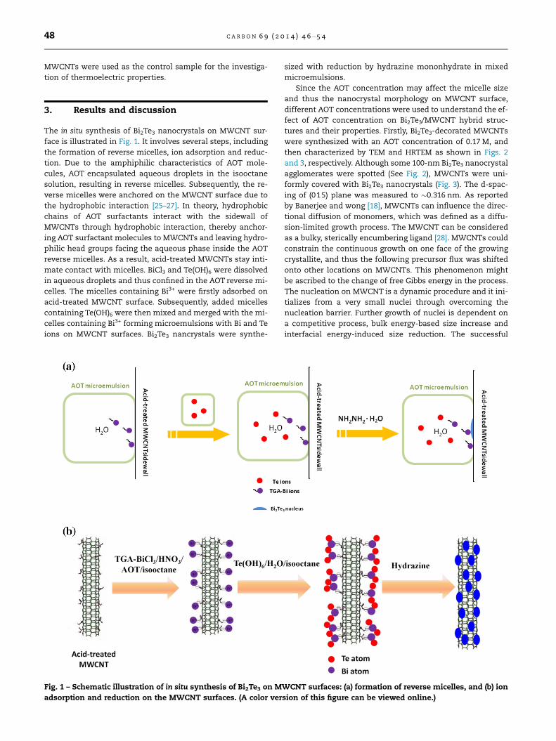
tures and their properties. Firstly, Bi2Te3-decorated MWCNTs
were synthesized with an AOT concentration of 0.17 M, and
then characterized by TEM and HRTEM as shown in Figs. 2
and 3, respectively. Although some 100-nm Bi2Te3 nanocrystal
agglomerates were spotted (See Fig. 2), MWCNTs were uni-
formly covered with Bi2Te3 nanocrystals (Fig. 3). The d-spac-
ing of (015) plane was measured to �0.316 nm. As reported
by Banerjee and wong [18], MWCNTs can influence the direc-
tional diffusion of monomers, which was defined as a diffu-
sion-limited growth process. The MWCNT can be considered
as a bulky, sterically encumbering ligand [28]. MWCNTs could
constrain the continuous growth on one face of the growing
crystallite, and thus the following precursor flux was shifted
onto other locations on MWCNTs. This phenomenon might
be ascribed to the change of free Gibbs energy in the process.
The nucleation on MWCNT is a dynamic procedure and it ini-
tializes from a very small nuclei through overcoming the
nucleation barrier. Further growth of nuclei is dependent on
a competitive process, bulk energy-based size increase and
interfacial energy-induced size reduction. The successful
WCNT surfaces: (a) formation of reverse micelles, and (b) ion
sion of this figure can be viewed online.)
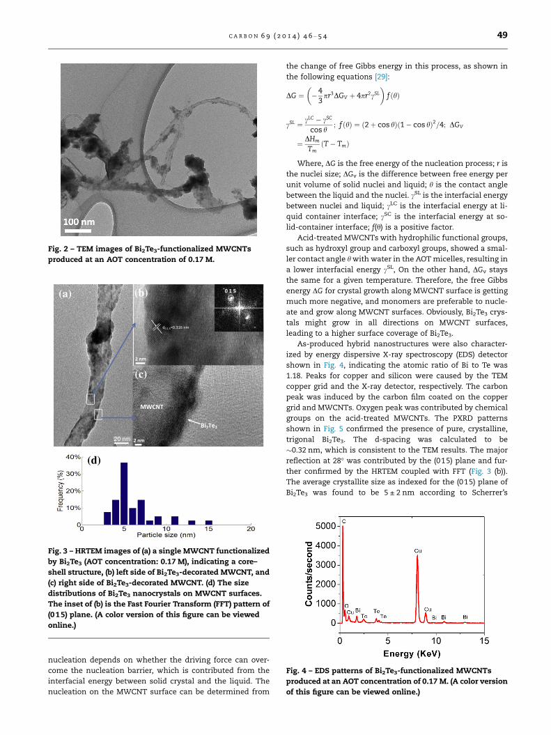
Fig. 2 – TEM images of Bi2Te3-functionalized MWCNTs
produced at an AOT concentration of 0.17 M.
MWCNT
(a) (b)
(c)
d0 1 5=0.316 nm
0 1 5
2 nm
2 nm
Bi2Te3
(d)
Fig. 3 – HRTEM images of (a) a single MWCNT functionalized
by Bi2Te3 (AOT concentration: 0.17 M), indicating a core–
shell structure, (b) left side of Bi2Te3-decorated MWCNT, and
(c) right side of Bi2Te3-decorated MWCNT. (d) The size
distributions of Bi2Te3 nanocrystals on MWCNT surfaces.
The inset of (b) is the Fast Fourier Transform (FFT) pattern of
(015) plane. (A color version of this figure can be viewed
online.)
Fig. 4 – EDS patterns of Bi2Te3-functionalized MWCNTs
produced at an AOT concentration of 0.17 M. (A color version
of this figure can be viewed online.)
C A R B O N 6 9 ( 2 0 1 4 ) 4 6 – 5 4 49
nucleation depends on whether the driving force can over-
come the nucleation barrier, which is contributed from the
interfacial energy between solid crystal and the liquid. The
nucleation on the MWCNT surface can be determined from
the change of free Gibbs energy in this process, as shown in
the following equations [29]:
DG ¼ �43
pr3DGV þ 4pr2cSL
� �fðhÞ
cSL ¼ cLC � cSC
cos h; fðhÞ ¼ ð2þ cos hÞð1� cos hÞ2=4; DGV
¼ DHm
TmðT� TmÞ
Where, DG is the free energy of the nucleation process; r is
the nuclei size; DGv is the difference between free energy per
unit volume of solid nuclei and liquid; h is the contact angle
between the liquid and the nuclei. cSL is the interfacial energy
between nuclei and liquid; cLC is the interfacial energy at li-
quid container interface; cSC is the interfacial energy at so-
lid-container interface; f(h) is a positive factor.
Acid-treated MWCNTs with hydrophilic functional groups,
such as hydroxyl group and carboxyl groups, showed a smal-
ler contact angle h with water in the AOT micelles, resulting in
a lower interfacial energy cSL, On the other hand, DGv stays
the same for a given temperature. Therefore, the free Gibbs
energy DG for crystal growth along MWCNT surface is getting
much more negative, and monomers are preferable to nucle-
ate and grow along MWCNT surfaces. Obviously, Bi2Te3 crys-
tals might grow in all directions on MWCNT surfaces,
leading to a higher surface coverage of Bi2Te3.
As-produced hybrid nanostructures were also character-
ized by energy dispersive X-ray spectroscopy (EDS) detector
shown in Fig. 4, indicating the atomic ratio of Bi to Te was
1.18. Peaks for copper and silicon were caused by the TEM
copper grid and the X-ray detector, respectively. The carbon
peak was induced by the carbon film coated on the copper
grid and MWCNTs. Oxygen peak was contributed by chemical
groups on the acid-treated MWCNTs. The PXRD patterns
shown in Fig. 5 confirmed the presence of pure, crystalline,
trigonal Bi2Te3. The d-spacing was calculated to be
�0.32 nm, which is consistent to the TEM results. The major
reflection at 28� was contributed by the (015) plane and fur-
ther confirmed by the HRTEM coupled with FFT (Fig. 3 (b)).
The average crystallite size as indexed for the (015) plane of
Bi2Te3 was found to be 5 ± 2 nm according to Scherrer’s
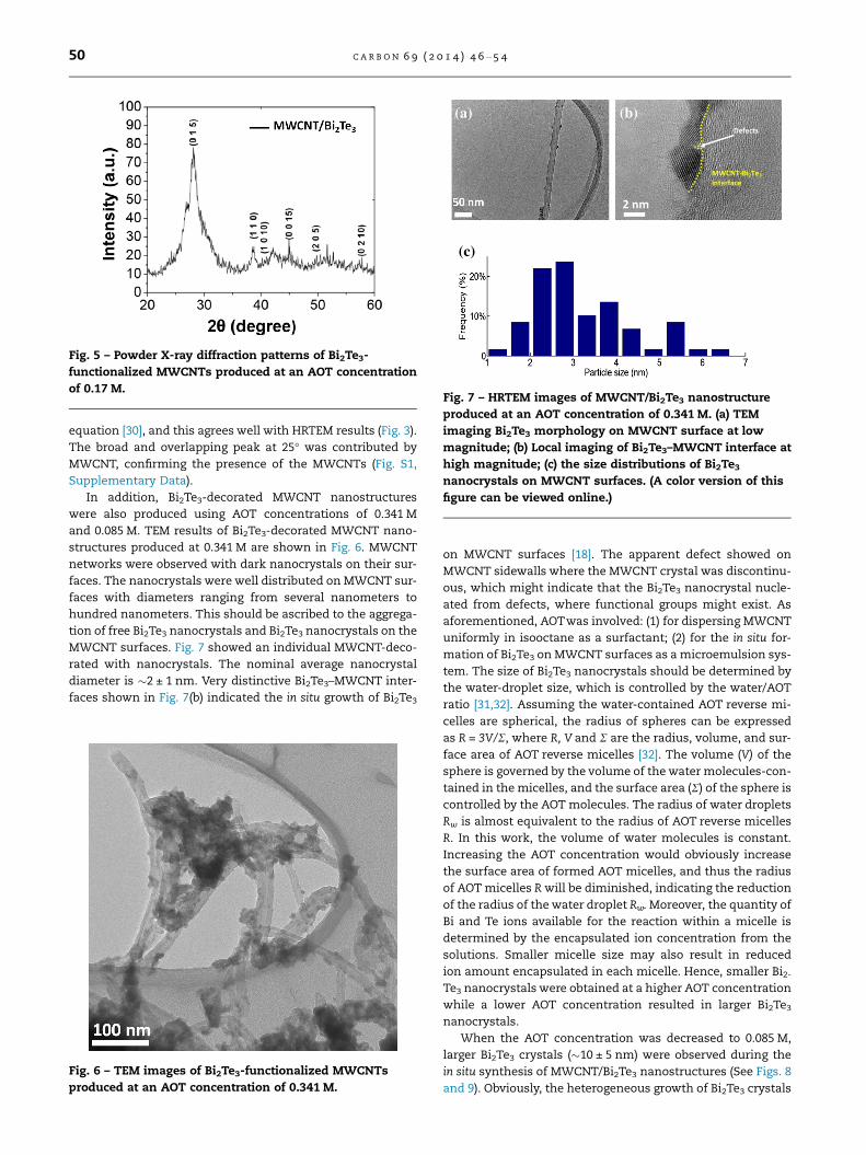
Fig. 5 – Powder X-ray diffraction patterns of Bi2Te3-
functionalized MWCNTs produced at an AOT concentration
of 0.17 M.
(c)
(a)
MWCNT-Bi2Te3 interface
Defects
2 nm
(b)
Fig. 7 – HRTEM images of MWCNT/Bi2Te3 nanostructure
produced at an AOT concentration of 0.341 M. (a) TEM
imaging Bi2Te3 morphology on MWCNT surface at low
magnitude; (b) Local imaging of Bi2Te3–MWCNT interface at
high magnitude; (c) the size distributions of Bi2Te3
nanocrystals on MWCNT surfaces. (A color version of this
figure can be viewed online.)
50 C A R B O N 6 9 ( 2 0 1 4 ) 4 6 – 5 4
equation [30], and this agrees well with HRTEM results (Fig. 3).
The broad and overlapping peak at 25� was contributed by
MWCNT, confirming the presence of the MWCNTs (Fig. S1,
Supplementary Data).
In addition, Bi2Te3-decorated MWCNT nanostructures
were also produced using AOT concentrations of 0.341 M
and 0.085 M. TEM results of Bi2Te3-decorated MWCNT nano-
structures produced at 0.341 M are shown in Fig. 6. MWCNT
networks were observed with dark nanocrystals on their sur-
faces. The nanocrystals were well distributed on MWCNT sur-
faces with diameters ranging from several nanometers to
hundred nanometers. This should be ascribed to the aggrega-
tion of free Bi2Te3 nanocrystals and Bi2Te3 nanocrystals on the
MWCNT surfaces. Fig. 7 showed an individual MWCNT-deco-
rated with nanocrystals. The nominal average nanocrystal
diameter is �2 ± 1 nm. Very distinctive Bi2Te3–MWCNT inter-
faces shown in Fig. 7(b) indicated the in situ growth of Bi2Te3
Fig. 6 – TEM images of Bi2Te3-functionalized MWCNTs
produced at an AOT concentration of 0.341 M.
on MWCNT surfaces [18]. The apparent defect showed on
MWCNT sidewalls where the MWCNT crystal was discontinu-
ous, which might indicate that the Bi2Te3 nanocrystal nucle-
ated from defects, where functional groups might exist. As
aforementioned, AOTwas involved: (1) for dispersing MWCNT
uniformly in isooctane as a surfactant; (2) for the in situ for-
mation of Bi2Te3 on MWCNT surfaces as a microemulsion sys-
tem. The size of Bi2Te3 nanocrystals should be determined by
the water-droplet size, which is controlled by the water/AOT
ratio [31,32]. Assuming the water-contained AOT reverse mi-
celles are spherical, the radius of spheres can be expressed
as R = 3V/R, where R, V and R are the radius, volume, and sur-
face area of AOT reverse micelles [32]. The volume (V) of the
sphere is governed by the volume of the water molecules-con-
tained in the micelles, and the surface area (R) of the sphere is
controlled by the AOT molecules. The radius of water droplets
Rw is almost equivalent to the radius of AOT reverse micelles
R. In this work, the volume of water molecules is constant.
Increasing the AOT concentration would obviously increase
the surface area of formed AOT micelles, and thus the radius
of AOT micelles R will be diminished, indicating the reduction
of the radius of the water droplet Rw. Moreover, the quantity of
Bi and Te ions available for the reaction within a micelle is
determined by the encapsulated ion concentration from the
solutions. Smaller micelle size may also result in reduced
ion amount encapsulated in each micelle. Hence, smaller Bi2-
Te3 nanocrystals were obtained at a higher AOT concentration
while a lower AOT concentration resulted in larger Bi2Te3
nanocrystals.
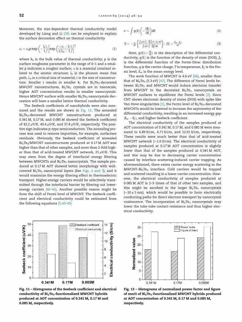
When the AOT concentration was decreased to 0.085 M,
larger Bi2Te3 crystals (�10 ± 5 nm) were observed during the
in situ synthesis of MWCNT/Bi2Te3 nanostructures (See Figs. 8
and 9). Obviously, the heterogeneous growth of Bi2Te3 crystals
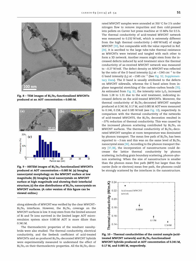
Fig. 8 – TEM images of Bi2Te3-functionalized MWCNTs
produced at an AOT concentration = 0.085 M.
(a)
(c)
(b) MWCNT-Bi2Te3 interface
5 nm
Fig. 9 – HRTEM images of Bi2Te3-functionalized MWCNTs
produced at AOT concentration = 0.085 M. (a) Imaging
nanocrystal morphology on the MWCNT surface at low
magnitude; (b) Imaging local nanocrystals on MWCNT
surface at high magnitude and showing their interfacial
structure; (c) the size distributions of Bi2Te3 nanocrystals on
MWCNT surfaces. (A color version of this figure can be
viewed online.)Acid-treated MWCNT network
Fig. 10 – Thermal conductivities of the control sample (acid-
treated MWCNT network) and Bi2Te3-functionalized
MWCNT hybrids produced at AOT concentration of 0.341 M,
0.17 M, and 0.085 M, respectively.
C A R B O N 6 9 ( 2 0 1 4 ) 4 6 – 5 4 51
along sidewalls of MWCNTwas verified by the clear MWCNT–
Bi2Te3 interfaces. However, the Bi2Te3 coverage on the
MWCNT surfaces is low. It may stem from the limited amount
of Bi and Te ions survived in the limited larger AOT micro-
emulsion system since 0.085 M AOT is more dilute than
0.341 M.
The thermoelectric properties of the resultant nanohy-
brids were also studied. The thermal conductivity, electrical
conductivity, and the Seebeck coefficient of acid-treated
MWCNTs and as-produced Bi2Te3-decorated MWCNT hybrids
were experimentally measured to understand the effect of
Bi2Te3 on their thermoelectric properties. All the Bi2Te3-deco-
rated MWCNT samples were annealed at 350 �C for 2 h under
nitrogen flow to remove impurities and then cold-pressed
into pellets on Carver hot press machine at 15 MPa for 0.5 h.
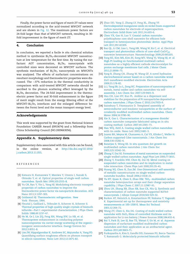
The thermal conductivity of acid-treated MWCNT network
was measured to 0.232 W/mK, which is extremely different
from the high thermal conductivity (�600 W/mK) of single
MWCNT [33], but comparable with the value reported in Ref.
[34]. It is ascribed to the large tube-tube thermal resistance
as MWCNTs were twisted and tangled with each other to
form a 3D network. Another reason might stem from the in-
creased defects induced by acid treatment since the thermal
conductivity of as-received MWCNT network was measured
to �0.27 W/mK. The defect density on MWCNT was reflected
by the ratio of the D band intensity (ID) at �1345 cm�1 to the
G band intensity (IG) at �1585 cm�1 (See Fig. S2, Supplemen-
tary Data). The D band is usually attributed to the defects
on MWCNT sidewalls, whereas the G band arises from in-
plane tangential stretching of the carbon–carbon bonds [35].
As estimated from Fig. S2, the intensity ratio ID/IG increased
from 1.28 to 1.31 due to the acid treatment, indicating in-
creased defects on the acid-treated MWCNTs. Moreover, the
thermal conductivity of Bi2Te3-decorated MWCNT samples
produced at 0.341 M, 0.17 M, and 0.085 M AOT were measured
to 0.146, 0.158, and 0.185 W/mK (see Fig. 10), respectively. In
comparison with the thermal conductivity of the networks
of acid-treated MWCNTS, the Bi2Te3 decoration resulted in
�37% reduction of thermal conductivity. This was caused by
the increased phonon scattering contributed by Bi2Te3 on
MWCNT surfaces. The thermal conductivity of Bi2Te3-deco-
rated MWCNT samples at room temperature was dominated
by phonon transport. The mean free path of Bi2Te3 has been
reported to �3 nm and this was on the same level of Bi2Te3
nanocrystal sizes [36]. According to the phonon transport the-
ory [37,38], the incorporation of nanostructures could de-
crease the lattice thermal conductivity by phonon
scattering, including grain boundary scattering, phonon–pho-
non scattering. When the size of nanostructure is smaller
than the phonon mean free path (MFP) but larger than the
carrier (hole or electron) mean free path, the phonons could
be strongly scattered by the interfaces in the nanostructure.
52 C A R B O N 6 9 ( 2 0 1 4 ) 4 6 – 5 4
Moreover, the size-dependent thermal conductivity model
developed by Liang and Li [39] can be employed to explain
the surface decoration effect on thermal conductivity
jl ¼ jbp exp � l0t
� �exp
�ða� 1Þt=L0 � 1
� �� �32
ð1Þ
where kb is the bulk value of thermal conductivity; p is the
surface roughness parameter in the range of 0–1 and a smal-
ler p indicates a rougher surface; a is a material constant re-
lated to the atomic structure; l0 is the phonon mean free
path, L0 is a critical size of material; t is the size of nanostruc-
ture. Smaller t results in smaller kl. For Bi2Te3-decorated
MWCNT nanostructures, Bi2Te3 crystals are in nanoscale,
higher AOT concentration results in smaller nanocrystals.
Hence MWCNT surface with smaller Bi2Te3 nanocrystals dec-
oration will have a smaller lattice thermal conductivity.
The Seebeck coefficients of nanohybrids were also mea-
sured and the results are shown in Fig. 11. The annealed
Bi2Te3-decorated MWCNT nanostructures produced at
0.341 M, 0.17 M, and 0.085 M showed the Seebeck coefficient
of 42.2 lV/K, 49.4 lV/K, and 37.8 lV/K, respectively. The posi-
tive sign indicates p-type semiconductors. The annealing pro-
cess was used to remove impurities, for example, surfactant
residuals. Obviously, the Seebeck coefficient of annealed
Bi2Te3/MWCNT nanostructures produced at 0.17 M AOT was
higher than that of other samples, and more than 2-fold high-
er than that of acid-treated MWCNT network, 21 lV/K. This
may stem from the degree of interfacial energy filtering
between MWCNTs and Bi2Te3 nanocrystals. The sample pro-
duced at 0.17 M AOT showed better morphology with well-
covered Bi2Te3 nanocrystal layers (See Figs. 2 and 3), and it
would maximize the energy filtering effect in thermoelectric
transport. Higher-energy carriers would be selectively trans-
mitted through the interfacial barrier by filtering out lower-
energy carriers [40–42]. Another possible reason might be
from the shift of Fermi level of MWCNT. The Seebeck coeffi-
cient and electrical conductivity could be estimated from
the following equations [5,43–45]
Fig. 11 – Histograms of the Seebeck coefficient and electrical
conductivity of Bi2Te3-functionalized MWCNT hybrids
produced at AOT concentration of 0.341 M, 0.17 M and
0.085 M, respectively.
r �Z
gðEÞ � @f0
@E
� �dE ð2Þ
S � � 1qT
RgðEÞ �@f0
@E
� �ðE�Ef ÞdER
gðEÞ �@f0@E
� �dE
� ; jSj � jEm�Ef j
qT ð3Þ
Here, gðEÞð� @f0@EÞ is the description of the differential con-
ductivity, gðEÞ is the function of the density-of state (DOS), f0
is the differential function of the Fermi–Dirac distribution
function, q is the carrier charge, T is temperature, Ef is the Fer-
mi level, Em is the mean energy level.
The work function of MWCNT is 4.6 eV [46], smaller than
that of Bi2Te3 (5.3 eV) [47]. The difference of Fermi levels be-
tween Bi2Te3 and MWCNT would induce electrons transfer
from MWCNT to the decorated Bi2Te3 nanocrystals on
MWCNT surfaces to equilibrate the Fermi levels [2]. Since
CNT shows electronic density of states (DOS) with spike-like
Van Hove singularities [1], the Fermi level of Bi2Te3-decorated
MWCNTs would be lowered to increase the asymmetry of the
differential conductivity, resulting in an increased energy gap
jEm � Ef j, and higher Seebeck coefficient.
The electrical conductivity of the samples produced at
AOT concentration of 0.341 M, 0.17 M, and 0.085 M were mea-
sured to 6.89 S/cm, 4.71 S/cm, and 12.01 S/cm, respectively.
These results were much better than that of acid-treated
MWCNT network (�1.6 S/cm). The electrical conductivity of
samples produced at 0.17 M AOT concentration is slightly
lower than that of the samples produced at 0.341 M AOT,
and this may be due to decreasing carrier concentration
caused by interface scattering-induced carrier trapping. As
aforementioned, there exists carrier energy scattering in the
MWCNT–Bi2Te3 interface. Cold carriers would be trapped
and scattered resulting in a lower carrier concentration. How-
ever, the electrical conductivity of samples produced at
0.085 M AOT is 2–3 times of that of other two samples, and
this might be ascribed to the larger Bi2Te3 nanocrystals
(�10 ± 5 nm), which would be possible to form electrically
conducting paths for direct electron transport by nanocrystal
coalescence. The incorporation of Bi2Te3 nanocrystals may
lower the tube-tube contact resistance and thus higher elec-
trical conductivity.
Fig. 12 – Histograms of normalized power factor and figure
of merit of Bi2Te3-functionalized MWCNT hybrids produced
at AOT concentration of 0.341 M, 0.17 M and 0.085 M,
respectively.
C A R B O N 6 9 ( 2 0 1 4 ) 4 6 – 5 4 53
Finally, the power factor and figure of merit ZT values were
normalized according to the acid-treated MWCNT network
and are shown in Fig. 12. The maximum power factors are
24-fold larger than that of MWCNT network, resulting in 30-
fold improvement in the figure of merit ZT.
4. Conclusion
In conclusion, we reported a facile in situ chemical solution
method to synthesize Bi2Te3-decorated MWCNT nanostruc-
ture at low temperature for the first time. By tuning the sur-
factant AOT concentration, Bi2Te3 nanocrystals with
controlled sizes were decorated on MWCNT surfaces. The
synthesis mechanism of Bi2Te3 nanocrystals on MWCNTs
was analyzed. The effects of surfactant concentrations on
resultant morphology and thermoelectric properties were dis-
cussed. The �37% reduction in the thermal conductivity in
comparison with acid-treated MWCNT networks should be
ascribed to the phonon scattering effect leveraged by the
Bi2Te3 decoration. The 24-fold improvement in the thermo-
electric power factor and 30-fold enhancement in the figure
of merit might result from the energy filtering effect at the
MWCNT–Bi2Te3 interfaces and the enlarged difference be-
tween the Fermi level and the mean transport energy level.
Acknowledgements
This work was supported by the grant from National Science
Foundation CAREER Award (0953674) and a fellowship from
China Scholarship Council (NO.2009663056).
Appendix A. Supplementary data
Supplementary data associated with this article can be found,
in the online version, at http://dx.doi.org/10.1016/
j.carbon.2013.11.055.
R E F E R E N C E S
[1] Kataura H, Kumazawa Y, Maniwa Y, Umezu I, Suzuki S,Ohtsuka Y, et al. Optical properties of single-wall carbonnanotubes. Synth Met 1999;103:2555–8.
[2] Yu CH, Ryu Y, Yin L, Yang HJ. Modulating electronic transportproperties of carbon nanotubes to improve thethermoelectric power factor via nanoparticle decoration. ACSNano 2011;5:1297–303.
[3] Goldsmid HJ. Thermoelectric refrigeration. NewYork: Plenum; 1964.
[4] Fleurial J, Gailliard L, Triboulet R, Scherrer H, Scherrer S.Thermal properties of high quality single crystals of bismuthtelluride—Part I: experimental characterization. J Phys ChemSolids 1988;49:1237–47.
[5] He M, Ge J, Lin ZQ, Feng XH, Wang XW, Lu HB, et al.Thermopower enhancement in conducting polymernanocomposites via carrier energy scattering at the organic–inorganic semiconductor interface. Energy Environ Sci2012;5:8351–8.
[6] Lim JW, Hippalgaonkar K, Andrews SC, Majumdar A, Yang PD.Quantifying surface roughness effects on phonon transportin silicon nanowires. Nano Lett 2012;12:2475–82.
[7] Zhao DD, Yang Z, Zhang LY, Feng XL, Zhang YF.Electrodeposited manganese oxide on nickel foam–supportedcarbon nanotubes for electrode of supercapacitors.Electrochem Solid-State Lett 2011;14:A93–6.
[8] Chen YX, Gao H, Luo Y. Coaxial carbon nanotube–polythiophene core-shell nanowire for efficient holetransport in heterojunction photovoltaic device. Appl PhysLett 2011;99:143309.
[9] Bao QL, Li CM, Liao L, Yang HB, Wang W, Ke C, et al. Electricaltransport and photovoltaic effects of core–shell CuO/C60
nanowire heterostructure. Nanotechnology 2009;20:065203.[10] Fang BZ, Kim MS, Kim JH, Song MY, Wang YJ, Wang HJ, et al.
High Pt loading on functionalized multiwall carbonnanotubes as a highly efficient cathode electrocatalyst forproton exchange membrane fuel cells. J Mater Chem2011;21:8066–73.
[11] Fang B, Zhang CH, Zhang W, Wang GF. A novel hydrazineelectrochemical sensor based on a carbon nanotube-wiredZnO nanoflower-modified electrode. Electrochim Acta2009;55:178–82.
[12] Li J, Tang SB, Lu L, Zeng HC. Preparation of nanocomposites ofmetals, metal oxides and carbon nanotubes via self-assembly. J Am Chem Soc 2007;129:9401–9.
[13] Hsu CH, Liao HY, Kuo PL. Aniline as a dispersant andstabilizer for the preparation of Pt nanoparticles deposited oncarbon nanotubes. J Phys Chem C 2010;114:7933–9.
[14] Sainsbury T, Fitzmaurice D. Templated assembly ofsemiconductor and insulator nanoparticles at the surface ofcovalently modified multiwalled carbon nanotubes. ChemMater 2004;16:3780–90.
[15] Xie X, Gao L. Characterization of a manganese dioxide/carbon nanotube composite fabricated using an in situcoating method. Carbon 2007;45:2365–73.
[16] Han WQ, Zettl A. Coating single-walled carbon nanotubeswith tin oxide. Nano Lett 2003;3:681–3.
[17] Juarez BH, Meyns M, Chanaewa A, Cai YX, Klinke C, Weller H.Carbon supported Cdse nanocrystals. J Am Chem Soc2008;130:15282–4.
[18] Banerjee S, Wong SS. In situ quantum dot growth onmultiwalled carbon nanotubes. J Am Chem Soc2003;125:10342–50.
[19] Zhang Y, Dai HJ. Formation of metal nanowires on suspendedsingle-walled carbon nanotubes. Appl Phys Lett 2000;77:3015.
[20] Zhang Y, Franklin NW, Chen RJ, Dai HJ. Metal coating onsuspended carbon nanotubes and its implication to metal-tube interaction. Chem Phys Lett 2000;331:35–41.
[21] Huang WJ, Chen H, Zuo JM. One-Dimensional self-assemblyof metallic nanostructures on single-walled carbon-nanotube bundles. Small 2006;2:1418–21.
[22] Yu HT, Quan X, Chen S, Zhao HM. TiO2�multiwalled carbonnanotube heterojunction arrays and their charge separationcapability. J Phys Chem C 2007;11:12987–91.
[23] Zhou LN, Zhang XB, Zhao XB, Sun CX, Niu Q. Synthesis andcharacterization of carbon nanotube supported Bi2Te3nanocrystals. J Alloys Compd 2010;502:329–32.
[24] Burkov AT, Heinrich A, Konstantinov PP, Nakama T, YagasakiK. Experimental set-up for thermopower and resistivitymeasurements at 100–1300 K. Meas Sci Technol2001;12:264–72.
[25] Wang ZY, Chen G, Xia DG. Coating of multi-walled carbonnanotube with SnO2 films of controlled thickness and itsapplication for Li-ion battery. J Power Sources 2008;184:432–6.
[26] Bai Y, Park IS, Lee SJ, Bae TS, Watari F, Uo M, et al. Aqueousdispersion of surfactant-modified multiwalled carbonnanotubes and their application as an antibacterial agent.Carbon 2011;49:3663–71.
[27] Purkayastha A, Kim S, Gandhi DD, Ganesan PG, Borca-TasciucT, Ramanath G. Molecularly protected bismuth telluride
54 C A R B O N 6 9 ( 2 0 1 4 ) 4 6 – 5 4
nanoparticles: microemulsion synthesis and thermoelectrictransport properties. Adv Mater 2006;18:2958–63.
[28] Banerjee S, Wong SS. Structural characterization, opticalproperties, and improved solubility of carbon nanotubesfunctionalized with Wilkinson’s catalyst. J Am Chem Soc2002;124:8940–8.
[29] Porter DA, Easterling KE. Phase transformations in metalsand alloys (3rd version). CRC Press; 1992.
[30] Scherrer P. Bestimmung der Grosse und der inneren Strukturvon Kolloidteilchen mittels Rontgenstrahlen. Nachr Ges WissGottingen 1918;26:98–100.
[31] Yan QY, Purkayastha A, Kim TY, Kroger R, Bose A, RamanathG. Synthesis and assembly of monodisperse high-coercivitySilicaCapped FePt nanomagnets of tunable size, composition,and thermal stability from microemulsions. Adv Mater2006;18:2569–73.
[32] Pileni MP. Reverse micelles as microreactors. J Phys Chem1993;97:6961–73.
[33] Fan X, Dickey EC, Eklund PC, Williams KA, Grigorian L,Buczko R, et al. Atomic arrangement of iodine atoms insidesingle-walled carbon nanotubes. J Phys Rev Lett 2000;84:4621.
[34] Prasher RS, Hu XJ, Chalopin Y, Mingo N, Lofgreen K, Volz S.Turning carbon nanotubes from exceptional heat conductorsinto insulators. Phys Rev Lett 2009;102:105901.
[35] Tchoul MN, Ford WT, Lolli G, Resasco DE, Arepalli S. Effect ofmild nitric acid oxidation on dispersability, size, andstructure of single-walled carbon nanotubes. Chem Mater2007;19:5765–72.
[36] Mavrokefalos A, Moore AL, Pettes MT, Shi L, Wang W, Li XG.Thermoelectric and structural characterizations of individualelectrodeposited bismuth telluride nanowires. J Appl Phys2009;105:104318.
[37] Hicks LD, Dresselhaus MS. Thermoelectric figure of merit of aone-dimensional conductor. Phys Rev B 1993;47:16631.
[38] Minnich AJ, Dresselhaus MS, Ren ZF, Chen G. Bulknanostructured thermoelectric materials: current researchand future prospects. Energy Environ Sci 2009;2:466–79.
[39] Liang LH, Li BW. Size-dependent thermal conductivity ofnanoscale semiconducting systems. Phys Rev B2006;73:153303.
[40] Chen J, Sun T, Sim DH, Peng HY, Wang HT, Fan SF, et al.Sb2Te3 nanoparticles with enhanced seebeck coefficient andlow thermal conductivity. Chem Mater 2010;22:3086–92.
[41] Martin J, Wang L, Chen L, Nolas GS. Enhanced seebeckcoefficient through energy-barrier scattering in PbTenanocomposites. Phys Rev B 2009;79:115311.
[42] Gao YW, He YZ, Zhu LL. Impact of grain size on the Seebeckcoefficient of bulk polycrystalline thermoelectric materials.Chin Sci Bull 2010;55:16–21.
[43] Young DL, Coutts TJ, Kaydanov VI, Gilmore AS, Mulligan WP.Direct measurement of density-of-states effective mass andscattering parameter in transparent conducting oxides usingsecond-order transport phenomena. J Vac Sci Technol, A2000;18:2978–85.
[44] Heremans JP, Thrush CM, Morelli DT. Thermopowerenhancement in lead telluride nanostructures. Phys Rev B2004;70:115334.
[45] Pichanusakorn P, Bandaru P. Nanostructured thermoelectric.Mat Sci Eng R 2010;67:19–63.
[46] Liu P, Wei Y, Jiang KL, Sun Q, Zhang XB, Fan SS. Thermionicemission and work function of multiwalled carbon nanotubeyarns. Phys Rev B 2006;73:235412.
[47] Haneman D. Adsorption and bonding properties of cleavagesurfaces of bismuth telluride. Phys Rev 1960;119:567–9.