Embed Size (px)
Citation preview
The University of Texas at Austin 1
Thermomechanical Characterization and Modeling for TSV Structures
Financial support from Semiconductor Research Corporation is gratefully acknowledged.
Rui Huang
Suk-Kyu Ryu, Tengfei Jiang, Kuan H. (Gary) Lu, Qiu Zhao, Jay Im and Paul S. Ho
Microelectronics Research Center
Dept. Aerospace Engineering & Engineering Mechanics
The University of Texas at Austin 2
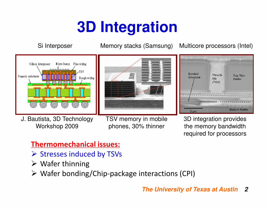
3D IntegrationMemory stacks (Samsung) Multicore processors (Intel)
TSV memory in mobile
phones, 30% thinner
3D integration provides
the memory bandwidth
required for processors
Si Interposer
J. Bautista, 3D Technology
Workshop 2009
Thermomechanical issues:
� Stresses induced by TSVs
� Wafer thinning
� Wafer bonding/Chip-package interactions (CPI)
The University of Texas at Austin 3
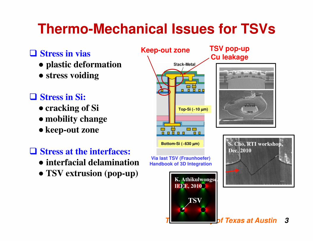
Thermo-Mechanical Issues for TSVs
� Stress in vias
● plastic deformation
● stress voiding
� Stress in Si:
● cracking of Si
●mobility change
● keep-out zone
� Stress at the interfaces:
● interfacial delamination
● TSV extrusion (pop-up)
S. Cho, RTI workshop,
Dec, 2010
TSV
K. Athikulwongse,
IEEE, 2010
TSV pop-upCu leakage
Keep-out zone
Via last TSV (Fraunhoefer)Handbook of 3D Integration
Top-Si (~10 µµµµm)
Bottom-Si (~630 µµµµm)
The University of Texas at Austin 4
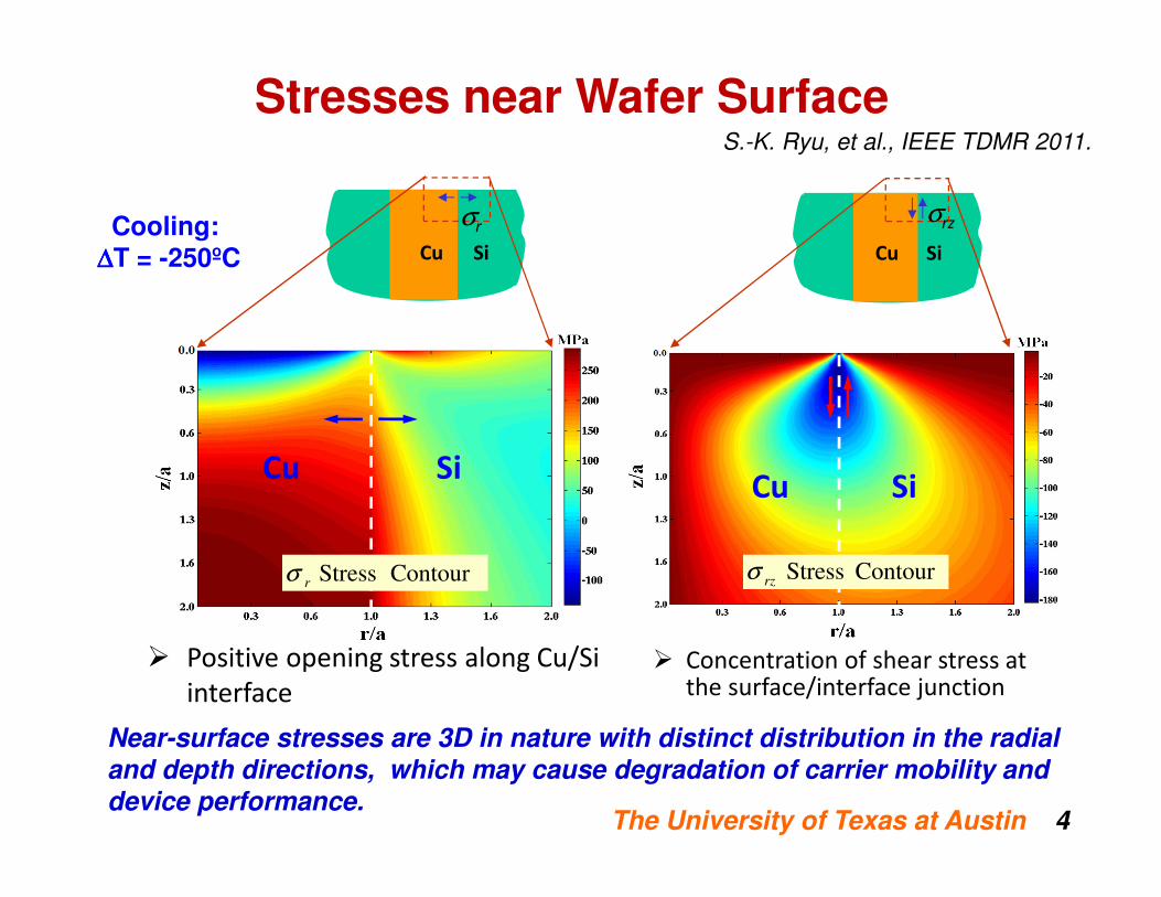
Stresses near Wafer Surface
Cu Si
� Concentration of shear stress at the surface/interface junction
SiCu
σrz
Cu Si
� Positive opening stress along Cu/Si
interface
SiCu
σr
Near-surface stresses are 3D in nature with distinct distribution in the radial and depth directions, which may cause degradation of carrier mobility and device performance.
S.-K. Ryu, et al., IEEE TDMR 2011.
Cooling: ∆∆∆∆T = -250ºC
Contour Stressrσ Contour Stressrzσ
The University of Texas at Austin 5
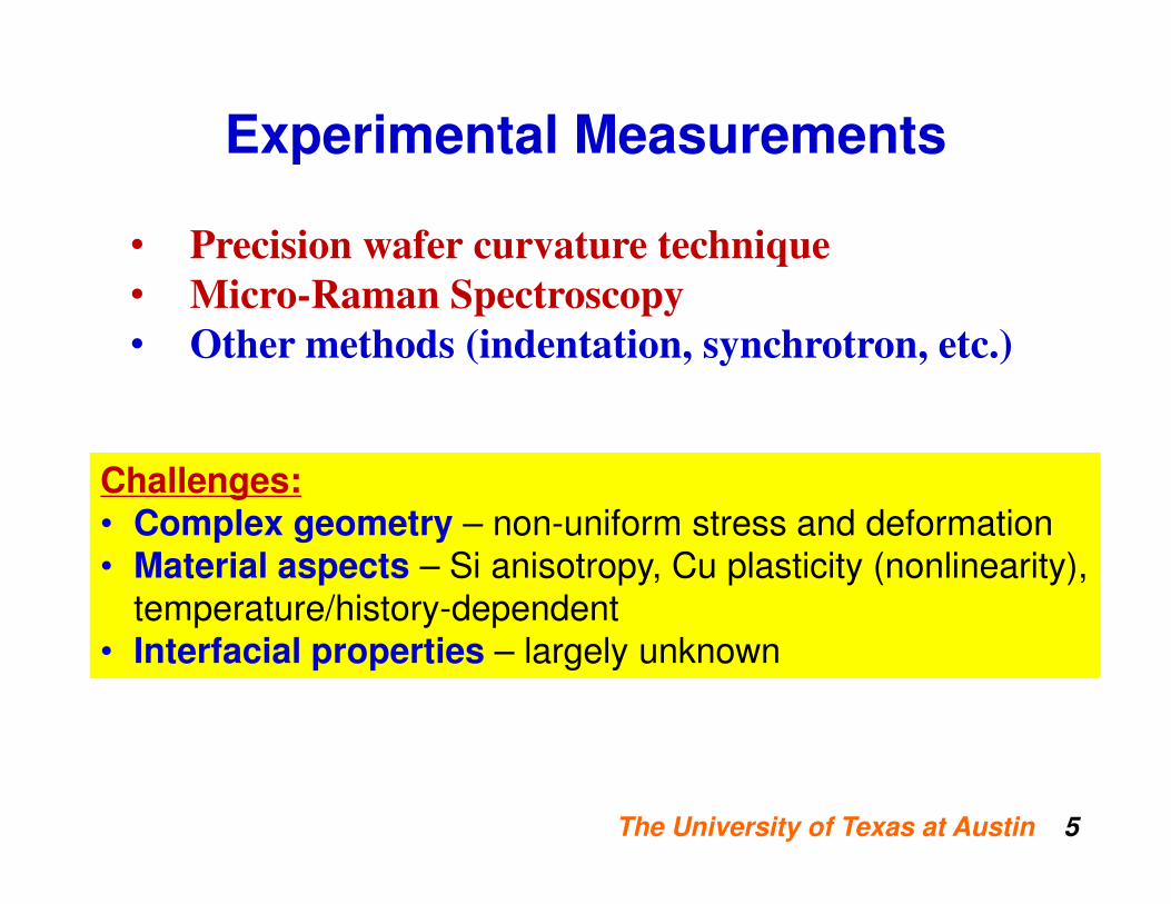
Experimental Measurements
• Precision wafer curvature technique
• Micro-Raman Spectroscopy
• Other methods (indentation, synchrotron, etc.)
Challenges:• Complex geometry – non-uniform stress and deformation
• Material aspects – Si anisotropy, Cu plasticity (nonlinearity),
temperature/history-dependent
• Interfacial properties – largely unknown
The University of Texas at Austin 6
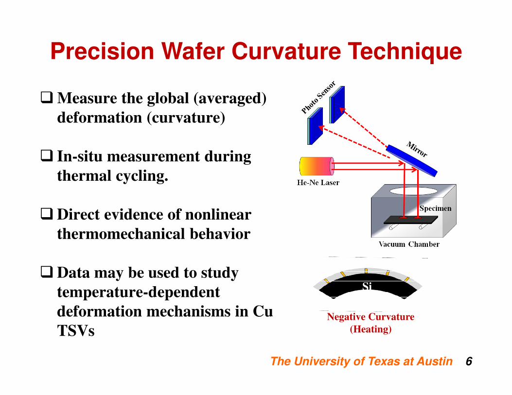
Precision Wafer Curvature Technique
� Measure the global (averaged)
deformation (curvature)
� In-situ measurement during
thermal cycling.
�Direct evidence of nonlinear
thermomechanical behavior
�Data may be used to study
temperature-dependent
deformation mechanisms in Cu
TSVsNegative Curvature
(Heating)
Si
The University of Texas at Austin 7
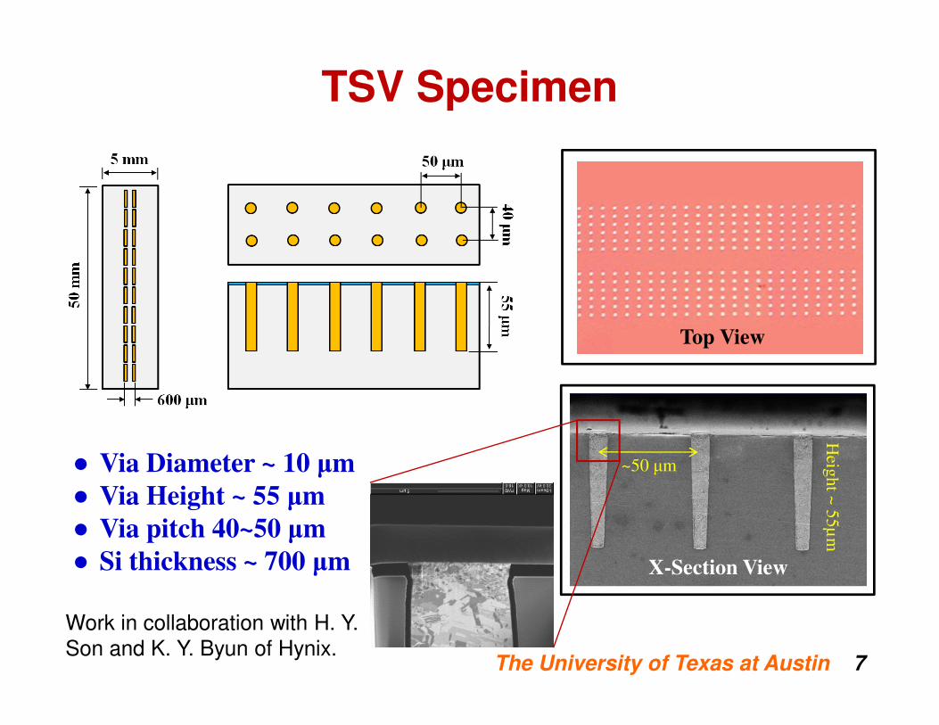
TSV Specimen
● Via Diameter ~ 10 µm
● Via Height ~ 55 µm
● Via pitch 40~50 µm
● Si thickness ~ 700 µm
Heig
ht ~
55
µm
~50 µm
Top View
X-Section View
Work in collaboration with H. Y.
Son and K. Y. Byun of Hynix.
The University of Texas at Austin 8
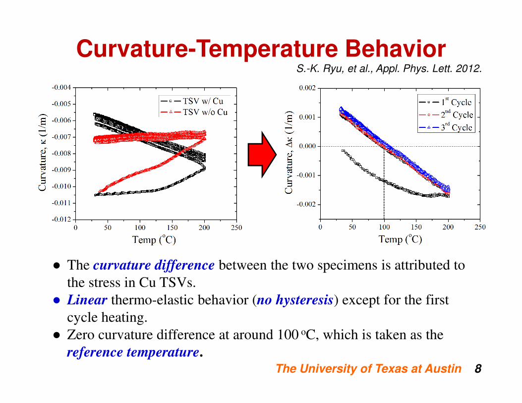
Curvature-Temperature Behavior
● The curvature difference between the two specimens is attributed to
the stress in Cu TSVs.
● Linear thermo-elastic behavior (no hysteresis) except for the first
cycle heating.
● Zero curvature difference at around 100 oC, which is taken as the
reference temperature.
S.-K. Ryu, et al., Appl. Phys. Lett. 2012.
The University of Texas at Austin 9
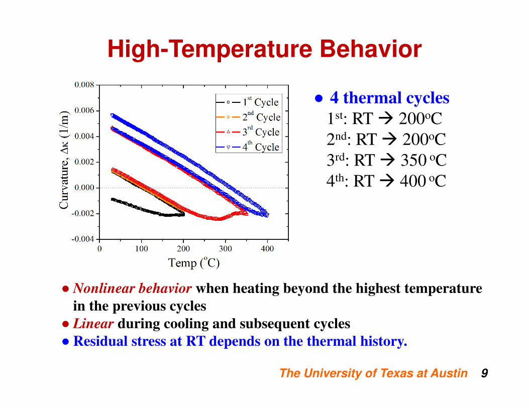
High-Temperature Behavior
● 4 thermal cycles
1st: RT � 200oC
2nd: RT � 200oC
3rd: RT � 350 oC
4th: RT � 400 oC
●Nonlinear behavior when heating beyond the highest temperature
in the previous cycles
● Linear during cooling and subsequent cycles
●Residual stress at RT depends on the thermal history.
The University of Texas at Austin 10
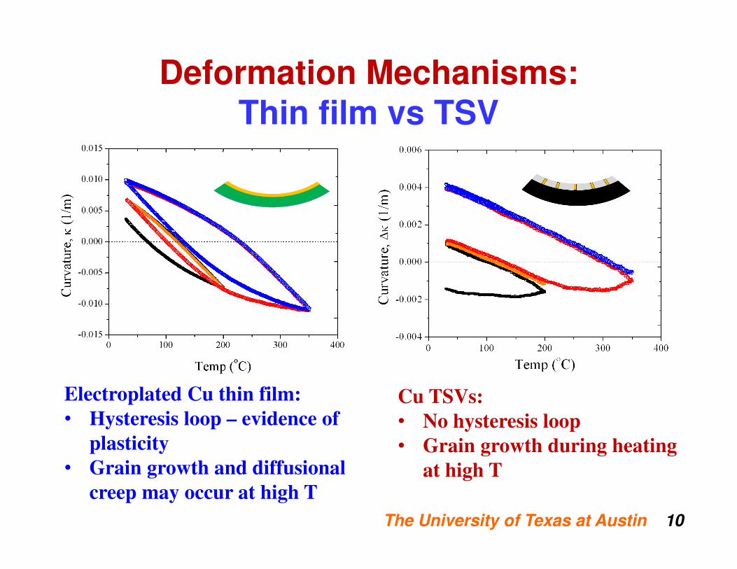
Deformation Mechanisms: Thin film vs TSV
Electroplated Cu thin film:
• Hysteresis loop – evidence of
plasticity
• Grain growth and diffusional
creep may occur at high T
Cu TSVs:
• No hysteresis loop
• Grain growth during heating
at high T
The University of Texas at Austin 11
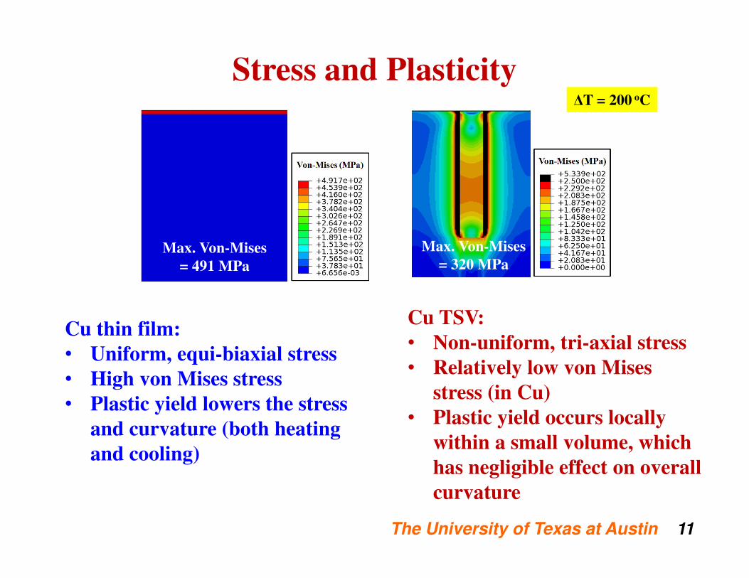
Stress and Plasticity
Max. Von-Mises
= 491 MPa
Max. Von-Mises
= 320 MPa
∆T = 200 oC
Cu thin film:
• Uniform, equi-biaxial stress
• High von Mises stress
• Plastic yield lowers the stress
and curvature (both heating
and cooling)
Cu TSV:
• Non-uniform, tri-axial stress
• Relatively low von Mises
stress (in Cu)
• Plastic yield occurs locally
within a small volume, which
has negligible effect on overall
curvature
The University of Texas at Austin 12
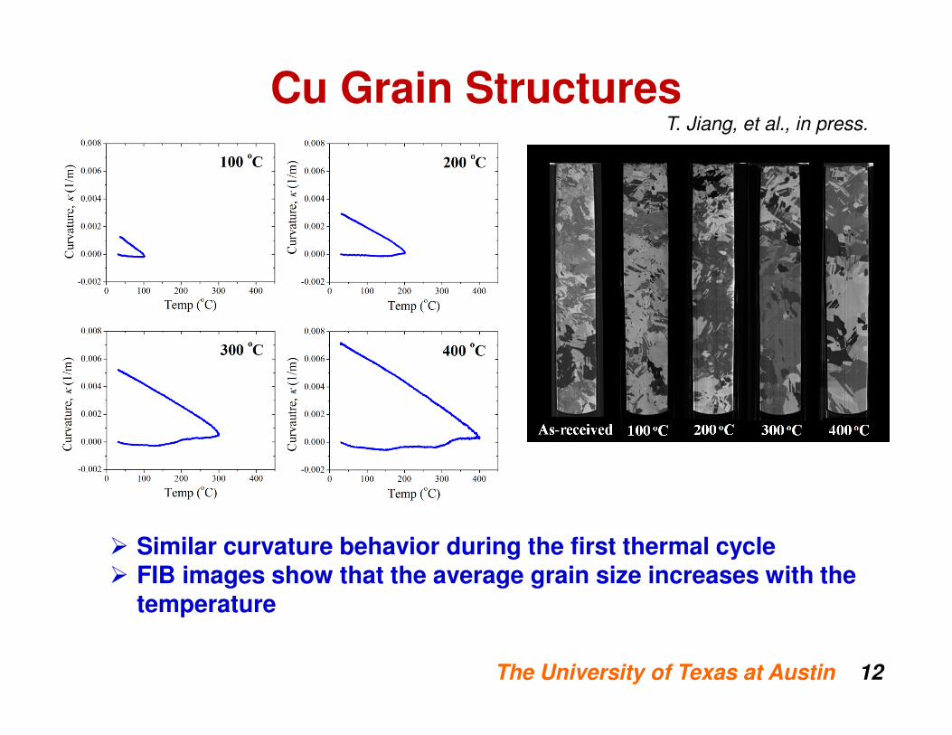
Cu Grain Structures
� Similar curvature behavior during the first thermal cycle� FIB images show that the average grain size increases with the
temperature
T. Jiang, et al., in press.
The University of Texas at Austin 13
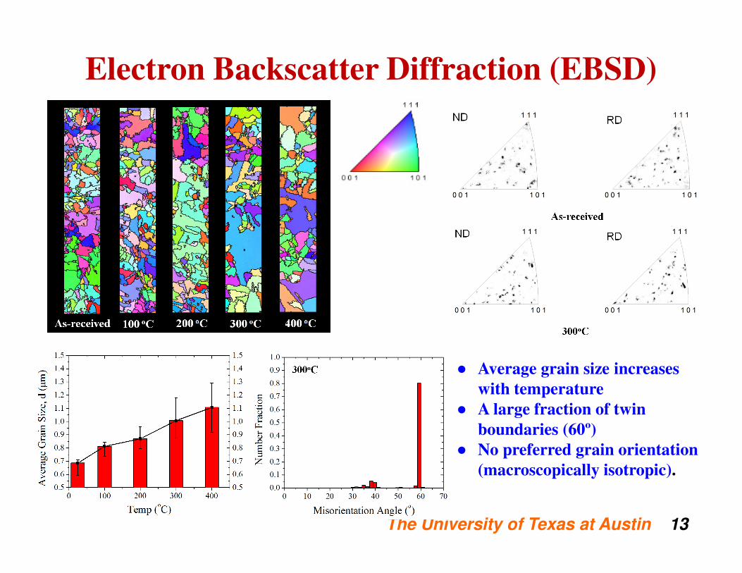
Electron Backscatter Diffraction (EBSD)
● Average grain size increases
with temperature
● A large fraction of twin
boundaries (60º)
● No preferred grain orientation
(macroscopically isotropic).
The University of Texas at Austin 14
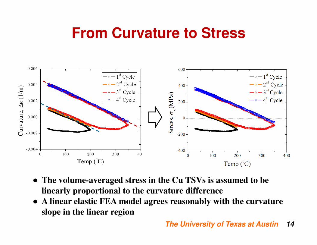
From Curvature to Stress
(a) BB Specimen
(b) Deformation (c) Lateral stress● The volume-averaged stress in the Cu TSVs is assumed to be
linearly proportional to the curvature difference
● A linear elastic FEA model agrees reasonably with the curvature
slope in the linear region
The University of Texas at Austin 15
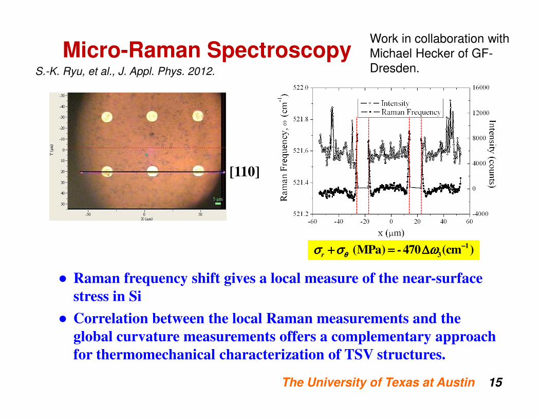
● Raman frequency shift gives a local measure of the near-surface
stress in Si
● Correlation between the local Raman measurements and the
global curvature measurements offers a complementary approach
for thermomechanical characterization of TSV structures.
Micro-Raman SpectroscopyWork in collaboration with
Michael Hecker of GF-
Dresden.
1
3(MPa) 470 (cm )
r-θθθθσ σ ωσ σ ωσ σ ωσ σ ω −−−−+ = ∆+ = ∆+ = ∆+ = ∆
[110]
S.-K. Ryu, et al., J. Appl. Phys. 2012.
The University of Texas at Austin 16
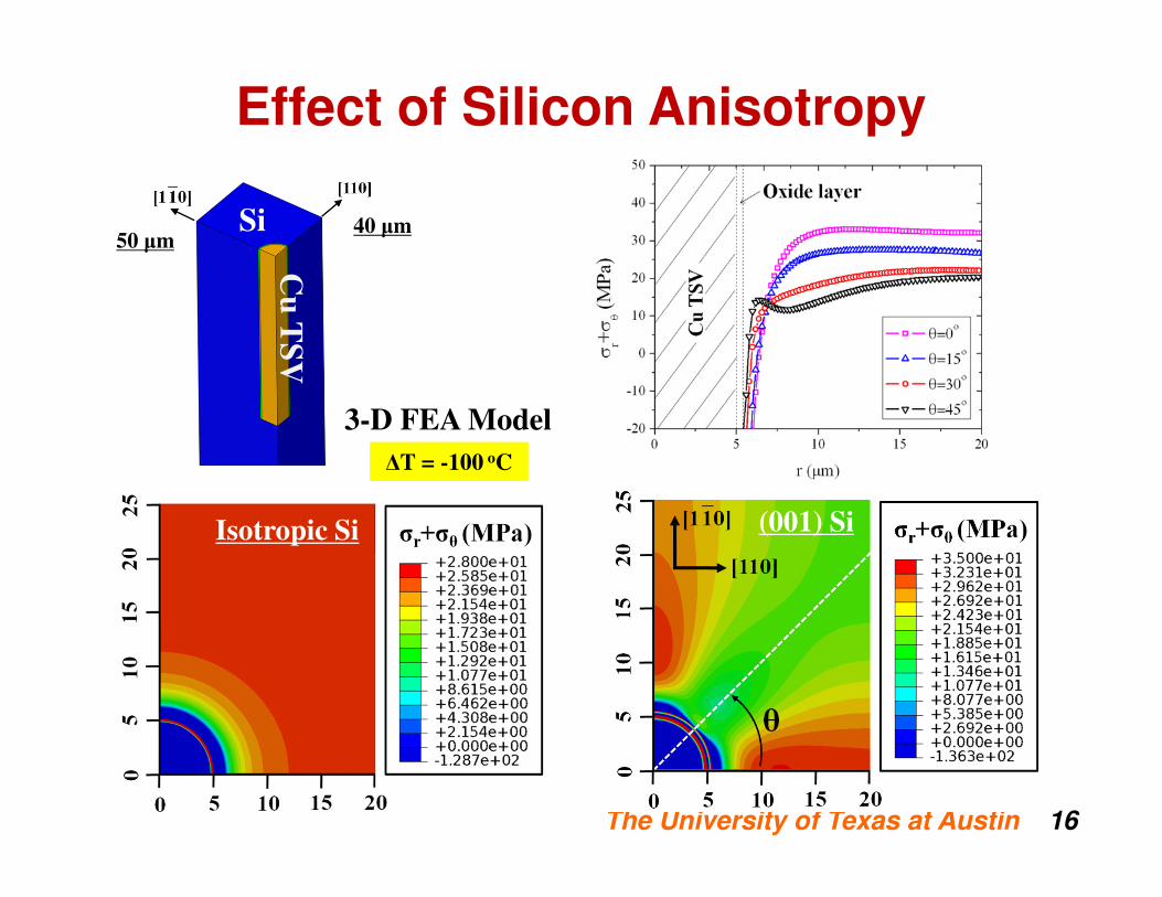
Effect of Silicon Anisotropy
Isotropic Si (001) Si
Si
Cu
TS
V
40 µm50 µm
3-D FEA Model
∆T = -100 oC
The University of Texas at Austin 17
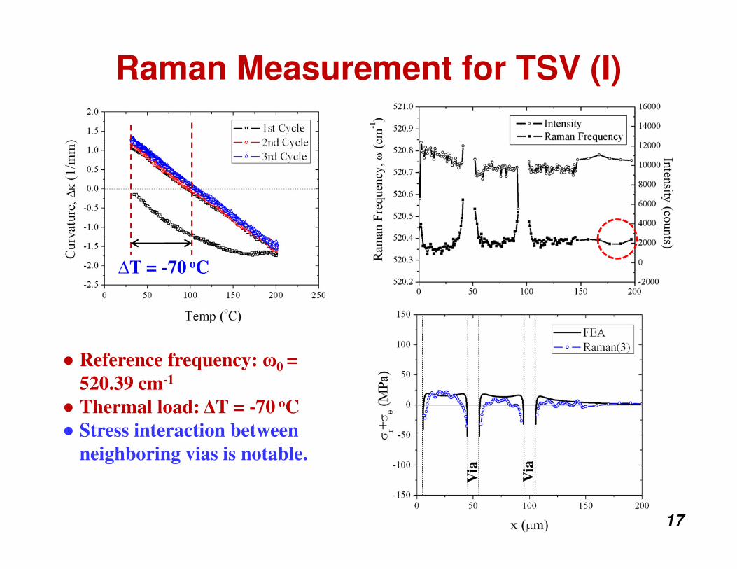
Raman Measurement for TSV (I)
∆T = -70 oC
● Reference frequency: ω0 =
520.39 cm-1
● Thermal load: ∆T = -70 oC
● Stress interaction between
neighboring vias is notable.V
ia
Via
The University of Texas at Austin 18
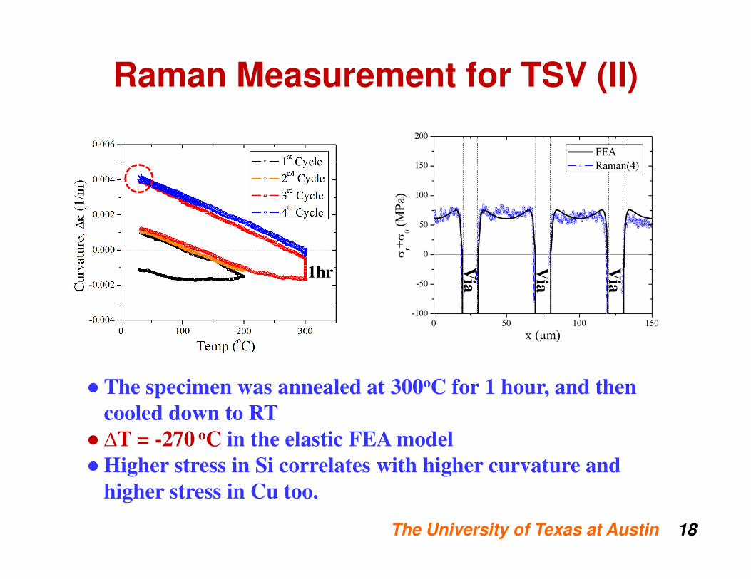
Raman Measurement for TSV (II)
●The specimen was annealed at 300oC for 1 hour, and then
cooled down to RT
● ∆T = -270 oC in the elastic FEA model
●Higher stress in Si correlates with higher curvature and
higher stress in Cu too.
1hrV
ia
Via
Via
The University of Texas at Austin 19
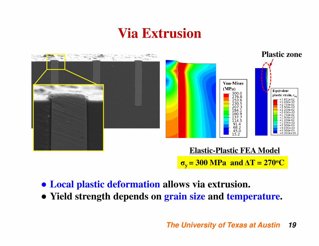
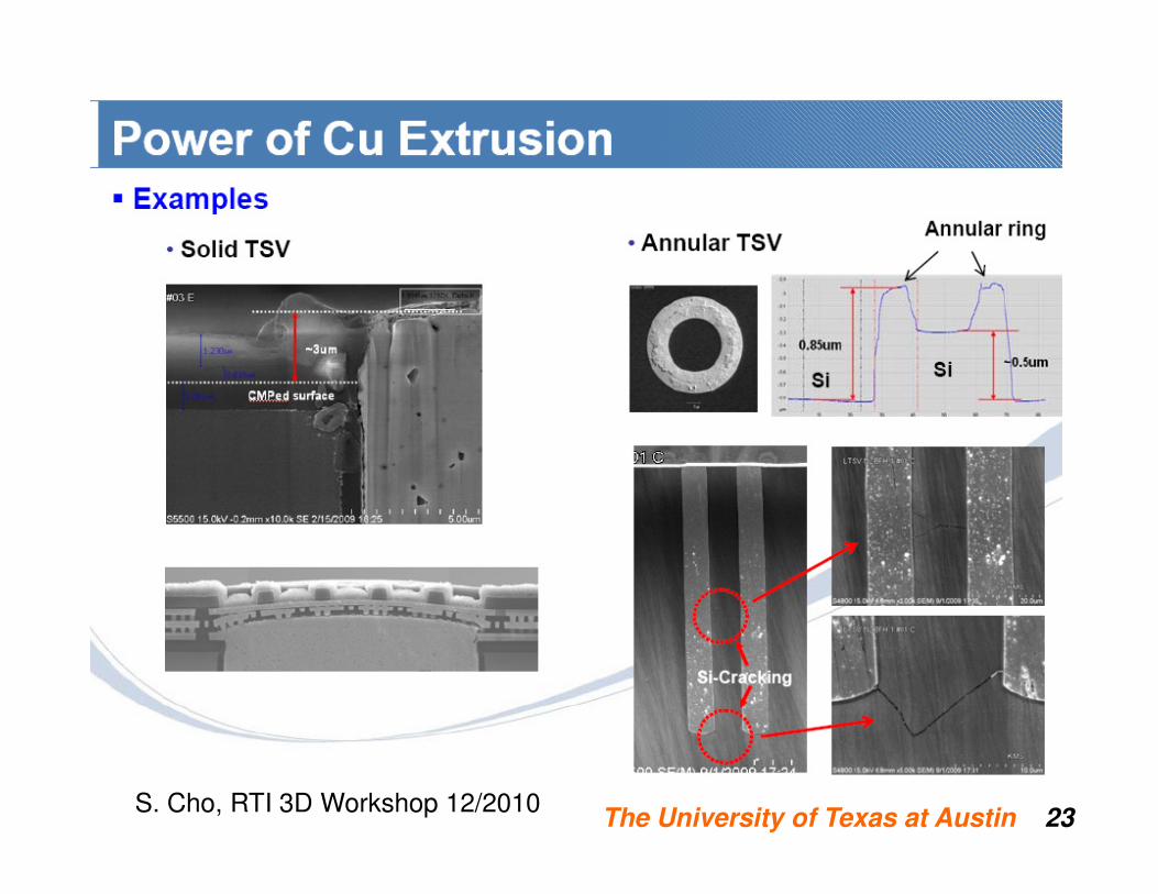
Via Extrusion
Via pop-up
● Local plastic deformation allows via extrusion.
● Yield strength depends on grain size and temperature.
σy = 300 MPa and ∆T = 270oC
Elastic-Plastic FEA Model
Plastic zone
The University of Texas at Austin 20
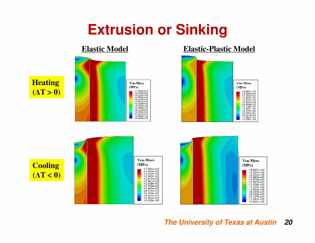
Extrusion or SinkingElastic-Plastic ModelElastic Model
Heating
(∆T > 0)
Cooling
(∆T < 0)
The University of Texas at Austin 21
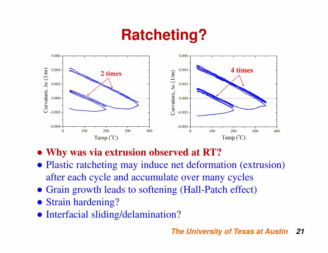
Ratcheting?
● Why was via extrusion observed at RT?
● Plastic ratcheting may induce net deformation (extrusion)
after each cycle and accumulate over many cycles
● Grain growth leads to softening (Hall-Patch effect)
● Strain hardening?
● Interfacial sliding/delamination?
The University of Texas at Austin 22
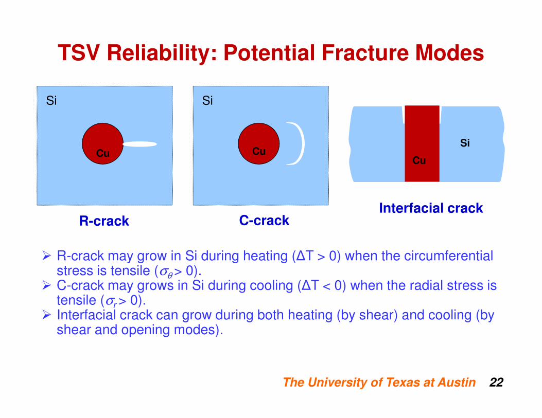
TSV Reliability: Potential Fracture Modes
Si Si
SiCuCu
R-crack C-crackInterfacial crack
� R-crack may grow in Si during heating (∆T > 0) when the circumferential stress is tensile (σθ > 0).
� C-crack may grows in Si during cooling (∆T < 0) when the radial stress is tensile (σr > 0).
� Interfacial crack can grow during both heating (by shear) and cooling (by shear and opening modes).
Cu
The University of Texas at Austin 23S. Cho, RTI 3D Workshop 12/2010
The University of Texas at Austin 24
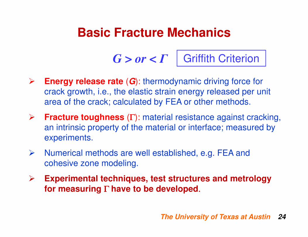
� Energy release rate (G): thermodynamic driving force for
crack growth, i.e., the elastic strain energy released per unit
area of the crack; calculated by FEA or other methods.
� Fracture toughness (ΓΓΓΓ): material resistance against cracking, an intrinsic property of the material or interface; measured by
experiments.
� Numerical methods are well established, e.g. FEA and
cohesive zone modeling.
� Experimental techniques, test structures and metrology
for measuring Γ Γ Γ Γ have to be developed....
Basic Fracture Mechanics
G > or < Γ Griffith Criterion
The University of Texas at Austin 25
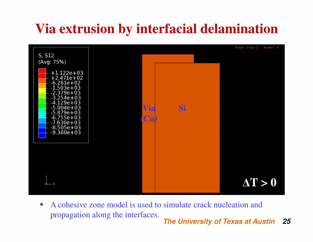
Via extrusion by interfacial delamination
� A cohesive zone model is used to simulate crack nucleation and
propagation along the interfaces.
∆T > 0
Via
(Cu)
Si
The University of Texas at Austin 26
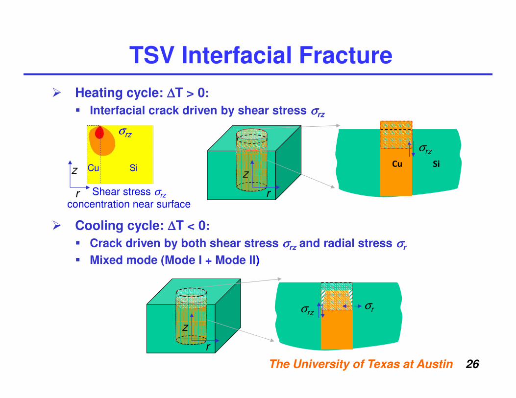
TSV Interfacial Fracture
� Heating cycle: ∆∆∆∆T > 0:
� Interfacial crack driven by shear stress σσσσrz
� Cooling cycle: ∆∆∆∆T < 0:
� Crack driven by both shear stress σσσσrz and radial stress σσσσr
� Mixed mode (Mode I + Mode II)
SiCu
σrz
r
z
σrz
r
z
σr
Shear stress σrz
concentration near surface
Cu Si
σrz
r
z
The University of Texas at Austin 27
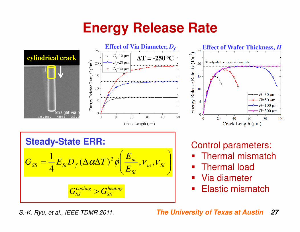
Energy Release RateEffect of Via Diameter, Df Effect of Wafer Thickness, H
∆T = -250 oCcylindrical crack
Steady-State ERR:
∆∆= Sim
Si
mfSiSS
E
ETDEG ννφα ,,)(
4
1 2
heating
SS
cooling
SS GG >
Control parameters:
� Thermal mismatch
� Thermal load
� Via diameter
� Elastic mismatch
S.-K. Ryu, et al., IEEE TDMR 2011.
The University of Texas at Austin 28
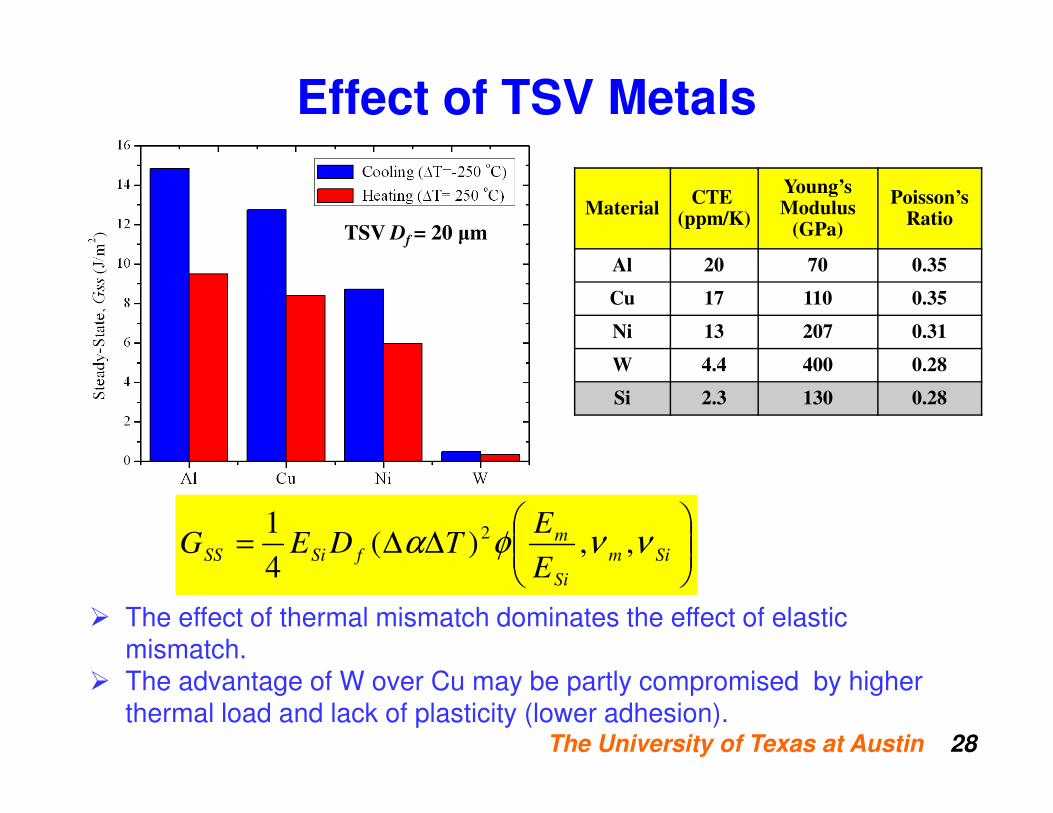
Effect of TSV Metals
TSV Df = 20 µm
MaterialCTE
(ppm/K)
Young’sModulus
(GPa)
Poisson’sRatio
Al 20 70 0.35
Cu 17 110 0.35
Ni 13 207 0.31
W 4.4 400 0.28
Si 2.3 130 0.28
� The effect of thermal mismatch dominates the effect of elastic mismatch.
� The advantage of W over Cu may be partly compromised by higher thermal load and lack of plasticity (lower adhesion).
∆∆= Sim
Si
mfSiSS
E
ETDEG ννφα ,,)(
4
1 2
The University of Texas at Austin 29
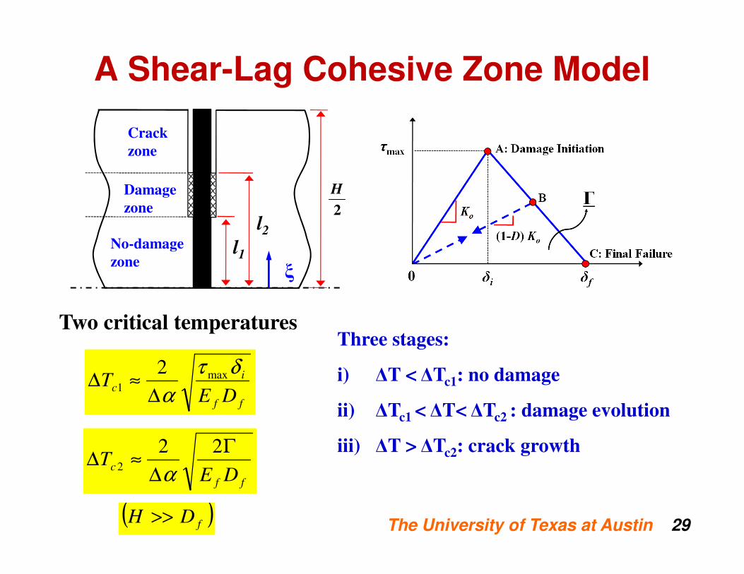
A Shear-Lag Cohesive Zone Model
Three stages:
i) ∆T < ∆Tc1: no damage
ii) ∆Tc1 < ∆T< ∆Tc2 : damage evolution
iii) ∆T > ∆Tc2: crack growth
Two critical temperatures
l1
l2
ξ
No-damage
zone
Damage
zone
Crack
zone
2
H
ff
ic
DET
δτ
αmax
1
2
∆≈∆
ff
cDE
TΓ
∆≈∆
222
α
( )fDH >>
The University of Texas at Austin 30
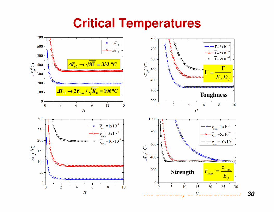
Critical Temperatures
1 max 02 / 196
cT K C∆ τ∆ τ∆ τ∆ τ→ = °→ = °→ = °→ = °
28Γ 333
cT C∆∆∆∆ → = °→ = °→ = °→ = °
Toughness
Strength
ff DE
Γ=Γ
fE
maxmax
ττ =
The University of Texas at Austin 31
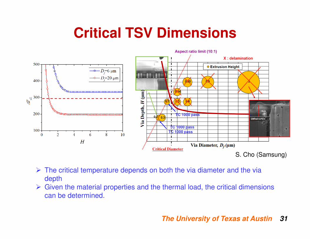
Critical TSV Dimensions
� The critical temperature depends on both the via diameter and the via
depth
� Given the material properties and the thermal load, the critical dimensions
can be determined.
S. Cho (Samsung)
The University of Texas at Austin 32
Summary
� Thermomechanical reliability of TSV structures has to be addressed by combining experimental characterization with modeling and simulations.
� Precision wafer curvature technique provides in-situ measurements of global deformation during thermal cycles.
� Micro-Raman spectroscopy provides local measurements of near-surface stress in Si, which can be correlated with the curvature measurements.
� Via extrusion may be induced by either local plastic deformation or interfacial delamination, to be further studied.
� Interfacial reliability of TSVs has been studied theoretically; More works are needed to characterize the interfacial properties and correlate modeling with experiments.
The University of Texas at Austin 33
Acknowledgments
H. Y. Son and K. Y. Byun, Hynix
Michael Hecker, Global Foundries, Dresden
Phil Garrou, Microelectronic Consultant, NC
Michael Lane, Emory and Henry College, VA
Mike Shapiro, IBM
Bob Jones and Zhihong Huang, Freescale
Funding Support: Semiconductor Research Corporation