Embed Size (px)
Citation preview
Time-Domain Magnetic Field Waveform Measurement Near Printed Circuit
Boards
TAKASHI HARADA, HIDEKI SASAKI, and EIJI HANKUINEC Corporation, Japan
SUMMARY
This paper describes a time domain magnetic field
measurement process for measuring magnetic fields near
printed circuit boards (PCBs) with a loop probe. In carrying
out these measurements, the loop probe needs to be cali-
brated in the frequency domain. In this process, a microstrip
line with a teflon substrate serving as the standard magnetic
field source is employed as a means of calibrating the probe.
The standard magnetic field intensities of the line are cal-
culated by using an approximate equation obtained from
Ampère�s law to simplify the calibration. The sensor-factor
of the probe obtained from this method agrees with that
obtained through the use of a standard G-TEM cell in 2 dB
at frequencies below 1 GHz. The waveforms of magnetic
fields near a PCB having a four-layer construction are
measured using a 10 mm diameter loop probe as the cali-
brated magnetic field sensor. The generation of magnetic
field waveforms causing the radiated emission from the
PCB is found to depend on the circuit operating conditions.
Our results clarify the fact that the time domain magnetic
field measurement process is an effective tool for analyzing
the sources of emission radiated from PCBs and for inves-
tigating the radiation mechanism. © 1998 Scripta Technica,
Electr Eng Jpn, 125(4): 9�18, 1998
Key words: Printed circuit board; magnetic field
intensity; time-domain measurement; spurious electromag-
netic wave radiation; EMI; microstrip line.
1. Introduction
Spurious radiation may be emitted from electronic
equipment. In order to deal with such radiation, the most
effective way is to suppress the radiation from the source
electronic circuit, as the source, as well as from the printed
circuit board on which the circuit is installed. Magnetic
field distribution measurements near PC boards have been
studied in order to specify the radiation sources of spurious
electromagnetic waves on the printed circuit board [1, 2].
The measurement is usually executed as follows. The
frequency characteristics at a particular frequency are
measured at a particular point on the board, or a sensor is
swept along the printed board to measure the magnetic field
at a particular frequency, and the intensity distribution is
displayed. These measurement methods benefit from the
fact that the source of radiation can be specified at the
component level, for example, ICs and the signal lines.
When the entire printed board is the source of radiation [3],
however, it is difficult to specify the source.
In order to deal with this problem, a technique to
measure the magnetic field near the printed board as a
time-domain waveform has been proposed [4, 5]. By ob-
serving the time-domain waveform, the time-course of the
magnetic field due to radiation can be interpreted in relation
to circuit operation. Consequently, useful information can
be obtained by analyzing the mechanism of radiation or
considering the suppression of the radiation.
The time-domain waveform of the magnetic field can
be derived by deconvolution of the output voltage wave-
form from the magnetic field sensor and the sensor factor,
which is the ratio of the magnetic field received by the
sensor and the output voltage [6]. Consequently, in the
measurements it is necessary to know beforehand the fre-
quency characteristics of the sensor factor. Since digital
signals have a wideband frequency spectrum, the sensor
factor must cover that bandwidth.
As a method for calibrating the magnetic field sensor,
the authors proposed a method using an unbalanced micro-
strip line that can generate a wideband magnetic field as a
standard magnetic field generation source [7]. This method
has the following additional advantages.
(1) The microstrip line can be assumed to generate,
with little error, the TEM mode, if the cross-sectional size
is sufficiently small compared to the wavelength. Thus, it
is easy to estimate the standard magnetic field intensity.
CCC0424-7760/98/040009-10
© 1998 Scripta Technica
Electrical Engineering in Japan, Vol. 125, No. 4, 1998Translated from Denki Gakkai Ronbunshi, Vol. 117-A, No. 5, May 1997, pp. 523�530
9
(2) If the propagation constant is known, the phase
on the line can be estimated. In other words, the phase can
be calibrated.
(3) The electromagnetic field intensity decreases
rapidly with distance from the line. Consequently, there is
less disturbance to the electromagnetic field by placing the
sensor and the connection cable far away from the line.
In this paper, a loop probe was used as the magnetic
field sensor. Initially, we describe the calibration of the
probe, using a microstrip line as the standard magnetic field
generation source. In order to simplify the calibration pro-
cedure, the magnetic field intensity near the line is repre-
sented by an expression derived from Ampère�s law. The
conditions for that approximation to be valid are discussed.
By comparing the result to that obtained by the usual
method, using a G-TEM cell as the standard magnetic field
source, the range over which the proposed method can be
applied is analyzed.
Using the loop probe calibrated as above, the time-
domain waveform of the magnetic field near a four-layer
printed circuit board with installed digital circuits is meas-
ured. It is demonstrated that the proposed measurement
procedure is useful in analyzing the spurious electromag-
netic wave radiation mechanism.
2. Measurement of Time-Domain Magnetic Field
Waveforms
The time-domain magnetic field waveform is ob-
tained as follows [6]. The output voltage waveform v(t) of
the loop probe is measured by an oscilloscope. Then, the
following manipulation is applied:
where f is the Fourier transform, and f-1is its inverse.
If the waveform does not contain a dc component, the
manipulation simplifies to
where F.(w) [A/V/m] is called the sensor factor [8]. This is
defined as the ratio H.(w) /V
.(w) of the frequency charac-
teristic H.(w) [A/m] of the received magnetic field to the
frequency characteristic V.(w) [V] of the output voltage. For
calculation contained in Eqs. (1) and (2), both the amplitude
and phase of the sensor factor must be known.
In general, calibration methods for the magnetic field
sensor can be classified as follows. In one method, a mag-
netic field with known intensity is generated by a standard
electromagnetic field generation source, such as a TEM cell
and loop antenna, and the ratio of the output voltage to the
known field intensity is calculated [9]. The other method is
a three-antenna method that uses three magnetic field sen-
sors and measures the transmission coefficients between
pairs of sensors [10]. In either case the factors of individual
sensors are obtained. In this paper, a microstrip line is used
as the standard magnetic field generation source and the
magnetic field around the line is used for calibration.
In the case of a microstrip line composed of a strip
conductor and the ground plane, the electromagnetic field
distribution in the cross section of the line is the TEM, as
shown in Fig. 1, if the width of the strip conductor and the
distance between the ground plane and the strip conductor
are sufficiently small compared to the wavelength. For a
microstrip line with dielectric support, the electromagnetic
field is not strictly TEM, but the distribution can be consid-
ered to have an approximate TEM mode if the permittivity
is low and the dielectric is thin. In this study, a microstrip
line with a teflon board is used and calibration is attempted
in the range from 10 MHz to 2 GHz.
3. Calibration Using a Microstrip Line
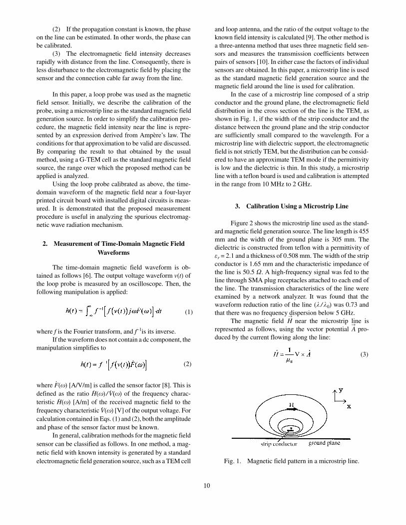
Figure 2 shows the microstrip line used as the stand-
ard magnetic field generation source. The line length is 455
mm and the width of the ground plane is 305 mm. The
dielectric is constructed from teflon with a permittivity of
er = 2.1 and a thickness of 0.508 mm. The width of the strip
conductor is 1.65 mm and the characteristic impedance of
the line is 50.5 W. A high-frequency signal was fed to the
line through SMA plug receptacles attached to each end of
the line. The transmission characteristics of the line were
examined by a network analyzer. It was found that the
waveform reduction ratio of the line (l /l0) was 0.73 and
that there was no frequency dispersion below 5 GHz.
The magnetic field H near the microstrip line is
represented as follows, using the vector potential A pro-
duced by the current flowing along the line:
(1)
(2)
Fig. 1. Magnetic field pattern in a microstrip line.
(3)
10
where m0 is the permeability of a vacuum.
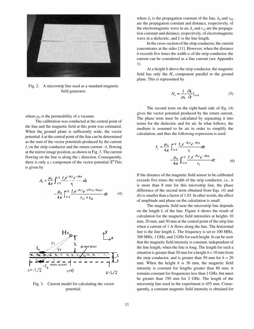
The calibration was conducted at the central point of
the line and the magnetic field at this point was estimated.
When the ground plane is sufficiently wide, the vector
potential A at the central point of the line can be determined
as the sum of the vector potentials produced by the current
Iz on the strip conductor and the return current -Iz flowing
at the mirror image position, as shown in Fig. 3. The current
flowing on the line is along the z direction. Consequently,
there is only a z component of the vector potential A®. This
is given by
where ks is the propagation constant of the line, k0 and r02
are the propagation constant and distance, respectively, of
the electromagnetic wave in air, kr and rr2 are the propaga-
tion constant and distance, respectively, of electromagnetic
wave in a dielectric, and L is the line length.
In the cross-section of the strip conductor, the current
concentrates at the sides [11]. However, when the distance
h exceeds five times the width w of the strip conductor, the
current can be considered as a line current (see Appendix
1).
At a height h above the strip conductor, the magnetic
field has only the Hx component parallel to the ground
plane. This is represented by
The second term on the right-hand side of Eq. (4)
gives the vector potential produced by the return current.
The phase term must be calculated by separating it into
terms for the dielectric and for air. In what follows, the
medium is assumed to be air in order to simplify the
calculation, and thus the following expression is used:
If the distance of the magnetic field sensor to be calibrated
exceeds five times the width of the strip conductor, i.e., it
is more than 8 mm for this microstrip line, the phase
difference of the second term obtained from Eqs. (4) and
(6) is smaller than a factor of 1.03. In other words, the effect
of amplitude and phase on the calculation is small.
The magnetic field near the microstrip line depends
on the length L of the line. Figure 4 shows the result of
calculation for the magnetic field intensities at heights 10
mm, 20 mm, and 30 mm at the central point of the strip line
when a current of 1 A flows along the line. The horizontal
line is the line length L. The frequency is set to 100 MHz,
300 MHz, 1 GHz, and 2 GHz for each height. It can be seen
that the magnetic field intensity is constant, independent of
the line length, when the line is long. The length for such a
situation is greater than 30 mm for a height h = 10 mm from
the strip conductor, and is greater than 50 mm for h = 20
mm. When the height h is 30 mm, the magnetic field
intensity is constant for lengths greater than 80 mm; it
remains constant for frequencies less than 1 GHz, but must
be greater than 350 mm for 2 GHz. The length of the
microstrip line used in the experiment is 455 mm. Conse-
quently, a constant magnetic field intensity is obtained for
Fig. 2. A microstrip line used as a standard magnetic
field generator.
Fig. 3. Current model for calculating the vector
potential.
(4)
(5)
(6)
11
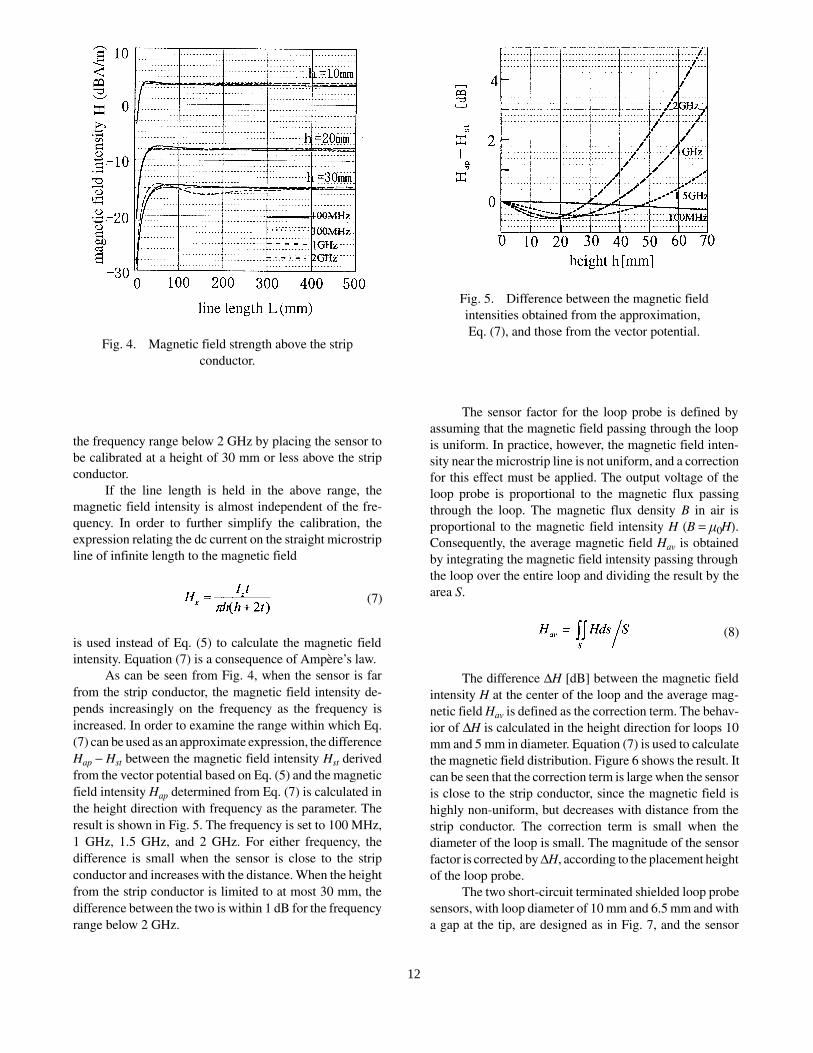
the frequency range below 2 GHz by placing the sensor to
be calibrated at a height of 30 mm or less above the strip
conductor.
If the line length is held in the above range, the
magnetic field intensity is almost independent of the fre-
quency. In order to further simplify the calibration, the
expression relating the dc current on the straight microstrip
line of infinite length to the magnetic field
is used instead of Eq. (5) to calculate the magnetic field
intensity. Equation (7) is a consequence of Ampère�s law.
As can be seen from Fig. 4, when the sensor is far
from the strip conductor, the magnetic field intensity de-
pends increasingly on the frequency as the frequency is
increased. In order to examine the range within which Eq.
(7) can be used as an approximate expression, the difference
Hap - Hst between the magnetic field intensity Hst derived
from the vector potential based on Eq. (5) and the magnetic
field intensity Hap determined from Eq. (7) is calculated in
the height direction with frequency as the parameter. The
result is shown in Fig. 5. The frequency is set to 100 MHz,
1 GHz, 1.5 GHz, and 2 GHz. For either frequency, the
difference is small when the sensor is close to the strip
conductor and increases with the distance. When the height
from the strip conductor is limited to at most 30 mm, the
difference between the two is within 1 dB for the frequency
range below 2 GHz.
The sensor factor for the loop probe is defined by
assuming that the magnetic field passing through the loop
is uniform. In practice, however, the magnetic field inten-
sity near the microstrip line is not uniform, and a correction
for this effect must be applied. The output voltage of the
loop probe is proportional to the magnetic flux passing
through the loop. The magnetic flux density B in air is
proportional to the magnetic field intensity H (B = m0H).
Consequently, the average magnetic field Hav is obtained
by integrating the magnetic field intensity passing through
the loop over the entire loop and dividing the result by the
area S.
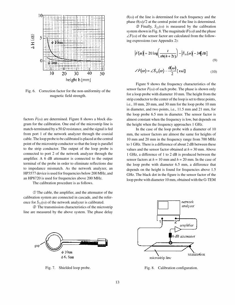
The difference DH [dB] between the magnetic field
intensity H at the center of the loop and the average mag-
netic field Hav is defined as the correction term. The behav-
ior of DH is calculated in the height direction for loops 10
mm and 5 mm in diameter. Equation (7) is used to calculate
the magnetic field distribution. Figure 6 shows the result. It
can be seen that the correction term is large when the sensor
is close to the strip conductor, since the magnetic field is
highly non-uniform, but decreases with distance from the
strip conductor. The correction term is small when the
diameter of the loop is small. The magnitude of the sensor
factor is corrected by DH, according to the placement height
of the loop probe.
The two short-circuit terminated shielded loop probe
sensors, with loop diameter of 10 mm and 6.5 mm and with
a gap at the tip, are designed as in Fig. 7, and the sensor
Fig. 4. Magnetic field strength above the strip
conductor.
(7)
Fig. 5. Difference between the magnetic field
intensities obtained from the approximation,
Eq. (7), and those from the vector potential.
(8)
12
factors F.(w) are determined. Figure 8 shows a block dia-
gram for the calibration. One end of the microstrip line is
match-terminated by a 50 W resistance, and the signal is fed
from port 1 of the network analyzer through the coaxial
cable. The loop probe to be calibrated is placed at the central
point of the microstrip conductor so that the loop is parallel
to the strip conductor. The output of the loop probe is
connected to port 2 of the network analyzer through the
amplifier. A 6 dB attenuator is connected to the output
terminal of the probe in order to eliminate reflections due
to impedance mismatch. As the network analyzer, an
HP3577 device is used for frequencies below 200 MHz, and
an HP8720 is used for frequencies above 200 MHz.
The calibration procedure is as follows.
À The cable, the amplifier, and the attenuator of the
calibration system are connected in cascade, and the refer-
ence for S.
21(w) of the network analyzer is calibrated.
Á The transmission characteristics of the microstrip
line are measured by the above system. The phase delay
q(w) of the line is determined for each frequency and the
phase q(w)/2 at the central point of the line is determined.
 Finally, S.
21(w) is measured by the calibration
system shown in Fig. 8. The magnitude |F.(w)| and the phase
ÐF.(w) of the sensor factor are calculated from the follow-
ing expressions (see Appendix 2):
Figure 9 shows the frequency characteristics of the
sensor factor F.(w) of each probe. The phase is shown only
for a loop probe with diameter 10 mm. The height from the
strip conductor to the center of the loop is set to three points,
i.e., 10 mm, 20 mm, and 30 mm for the loop probe 10 mm
in diameter, and two points, i.e., 11.5 mm and 21 mm, for
the loop probe 6.5 mm in diameter. The sensor factor is
almost constant when the frequency is low, but depends on
the height when the frequency approaches 1 GHz.
In the case of the loop probe with a diameter of 10
mm, the sensor factors are almost the same for heights of
10 mm and 20 mm in the frequency range from 700 MHz
to 1 GHz. There is a difference of about 2 dB between these
values and the sensor factor obtained at h = 30 mm. Above
1 GHz, a difference of 1 to 2 dB is produced between the
sensor factors at h = 10 mm and h = 20 mm. In the case of
the loop probe with diameter 6.5 mm, a difference that
depends on the height is found for frequencies above 1.5
GHz. The black dot in the figure is the sensor factor of the
loop probe with diameter 10 mm, obtained with the G-TEM
Fig. 6. Correction factor for the non-uniformity of the
magnetic field strength.
Fig. 7. Shielded loop probe.
(9)
(10)
Fig. 8. Calibration configuration.
13
cell as the standard magnetic field generation source. The
results agree to within 2 dB, except for a few frequencies.
From those results it can be seen that a calibration
equivalent to the conventional method is achieved by the
proposed method for frequencies less than 1 GHz by re-
stricting the height above the strip conductor to less than 20
mm. The reason for the dependency of the amplitude on
height at higher frequencies is presumably the deviation
from the TEM mode as one moves away from the line. The
details, however, are still being investigated.
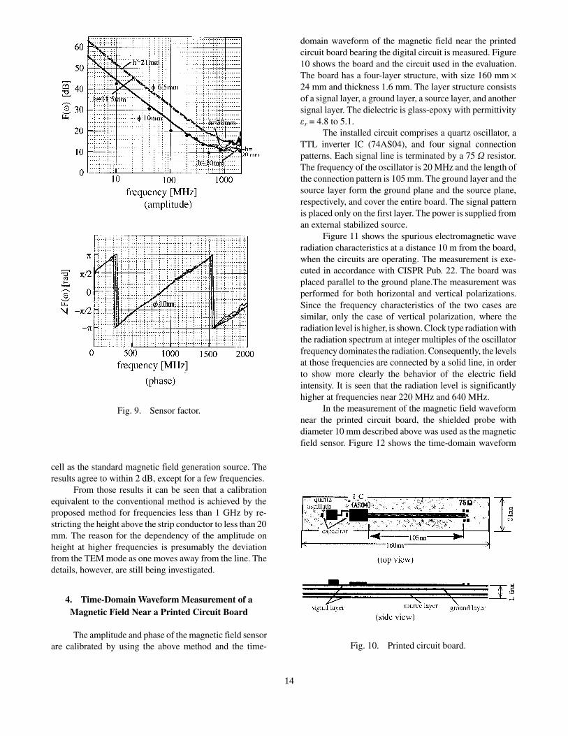
4. Time-Domain Waveform Measurement of a
Magnetic Field Near a Printed Circuit Board
The amplitude and phase of the magnetic field sensor
are calibrated by using the above method and the time-
domain waveform of the magnetic field near the printed
circuit board bearing the digital circuit is measured. Figure
10 shows the board and the circuit used in the evaluation.
The board has a four-layer structure, with size 160 mm ´
24 mm and thickness 1.6 mm. The layer structure consists
of a signal layer, a ground layer, a source layer, and another
signal layer. The dielectric is glass-epoxy with permittivity
er = 4.8 to 5.1.
The installed circuit comprises a quartz oscillator, a
TTL inverter IC (74AS04), and four signal connection
patterns. Each signal line is terminated by a 75 W resistor.
The frequency of the oscillator is 20 MHz and the length of
the connection pattern is 105 mm. The ground layer and the
source layer form the ground plane and the source plane,
respectively, and cover the entire board. The signal pattern
is placed only on the first layer. The power is supplied from
an external stabilized source.
Figure 11 shows the spurious electromagnetic wave
radiation characteristics at a distance 10 m from the board,
when the circuits are operating. The measurement is exe-
cuted in accordance with CISPR Pub. 22. The board was
placed parallel to the ground plane.The measurement was
performed for both horizontal and vertical polarizations.
Since the frequency characteristics of the two cases are
similar, only the case of vertical polarization, where the
radiation level is higher, is shown. Clock type radiation with
the radiation spectrum at integer multiples of the oscillator
frequency dominates the radiation. Consequently, the levels
at those frequencies are connected by a solid line, in order
to show more clearly the behavior of the electric field
intensity. It is seen that the radiation level is significantly
higher at frequencies near 220 MHz and 640 MHz.
In the measurement of the magnetic field waveform
near the printed circuit board, the shielded probe with
diameter 10 mm described above was used as the magnetic
field sensor. Figure 12 shows the time-domain waveform
Fig. 9. Sensor factor.
Fig. 10. Printed circuit board.
14
of the magnetic field at a point 10 mm above the signal
connection pattern. The magnetic field above the connec-
tion pattern exhibits a waveform in which an oscillation
with a period of approximately 4.5 ns is superposed on a
rectangular wave with a period of 50 ns and a duty ratio of
approximately 50%. The frequency of the rectangular wave
is 20 MHz and that of the sinusoidal oscillation is 220 MHz.
The 20 MHz rectangular wave is equal to the frequency of
the quartz oscillator. Since the connection pattern is resis-
tor-terminated, it is presumed to be the magnetic field
produced by the current flowing on the connection pattern
accompanying the operation of the ICs.
220 MHz, on the other hand, agrees with the fre-
quency of the spurious radiation of the highest level. In
other words, this sinusoidal oscillation is considered to be
the source of the spurious radiation. It is also seen, by
observing the waveform, that the 220 MHz oscillation is
produced when IC is at the high level, i.e., when the current
is flowing in the circuit. These results suggest that the
spurious radiation of the electromagnetic field depends on
the operating condition of the circuit. It has been difficult
to identify this behavior from previous measurements of the
magnetic field in the frequency domain.
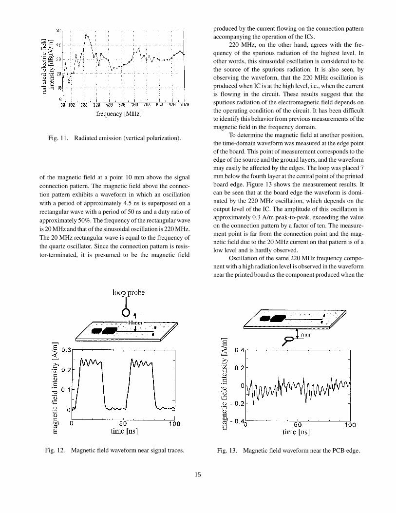
To determine the magnetic field at another position,
the time-domain waveform was measured at the edge point
of the board. This point of measurement corresponds to the
edge of the source and the ground layers, and the waveform
may easily be affected by the edges. The loop was placed 7
mm below the fourth layer at the central point of the printed
board edge. Figure 13 shows the measurement results. It
can be seen that at the board edge the waveform is domi-
nated by the 220 MHz oscillation, which depends on the
output level of the IC. The amplitude of this oscillation is
approximately 0.3 A/m peak-to-peak, exceeding the value
on the connection pattern by a factor of ten. The measure-
ment point is far from the connection point and the mag-
netic field due to the 20 MHz current on that pattern is of a
low level and is hardly observed.
Oscillation of the same 220 MHz frequency compo-
nent with a high radiation level is observed in the waveform
near the printed board as the component produced when the
Fig. 11. Radiated emission (vertical polarization).
Fig. 12. Magnetic field waveform near signal traces. Fig. 13. Magnetic field waveform near the PCB edge.
15
IC is at the high level and current is provided to the circuit.
In addition, the amplitude is high near the edge of the
printed board, where the effect of the source and the ground
layers are observed. From this perspective, it seems highly
probable that the radiation source of the spurious electro-
magnetic field in this printed board is in the source-ground
system.
5. Conclusions
This paper has discussed measurement of the time-
domain waveform of the magnetic field near a printed
circuit board, as well as the calibration of the loop probe to
be used for waveform measurement. A calibration method
is proposed in which the quasi-TEM mode produced by the
microstrip line is used as the standard magnetic field. Using
a microstrip line 455 mm long and with a ground plane
width of 305 mm on a teflon board of relative permittivity
2.1 and thickness 0.508 mm, the accuracy of the calibration
is examined. It was found that, even if the approximate
expression derived from Ampère�s law is used in the calcu-
lation of the standard magnetic field in order to simplify the
calibration procedure, a calibration factor almost equivalent
to the case in which a G-TEM cell is used as the standard
magnetic field generation source is obtained in the fre-
quency range below 1 GHz if the loop is placed within 20
mm of the strip conductor.
Using the loop probe calibrated by the proposed
method, the time-domain waveform of the magnetic field
is measured near the four-layer printed circuit board. It was
shown that a high-frequency magnetic field contributing to
the spurious electromagnetic wave radiation is produced,
depending on the operating state of the circuit. Thus, meas-
urement of the time-domain waveform is a useful means of
locating the source of spurious electromagnetic wave radia-
tion or of analyzing the mechanism of radiation.
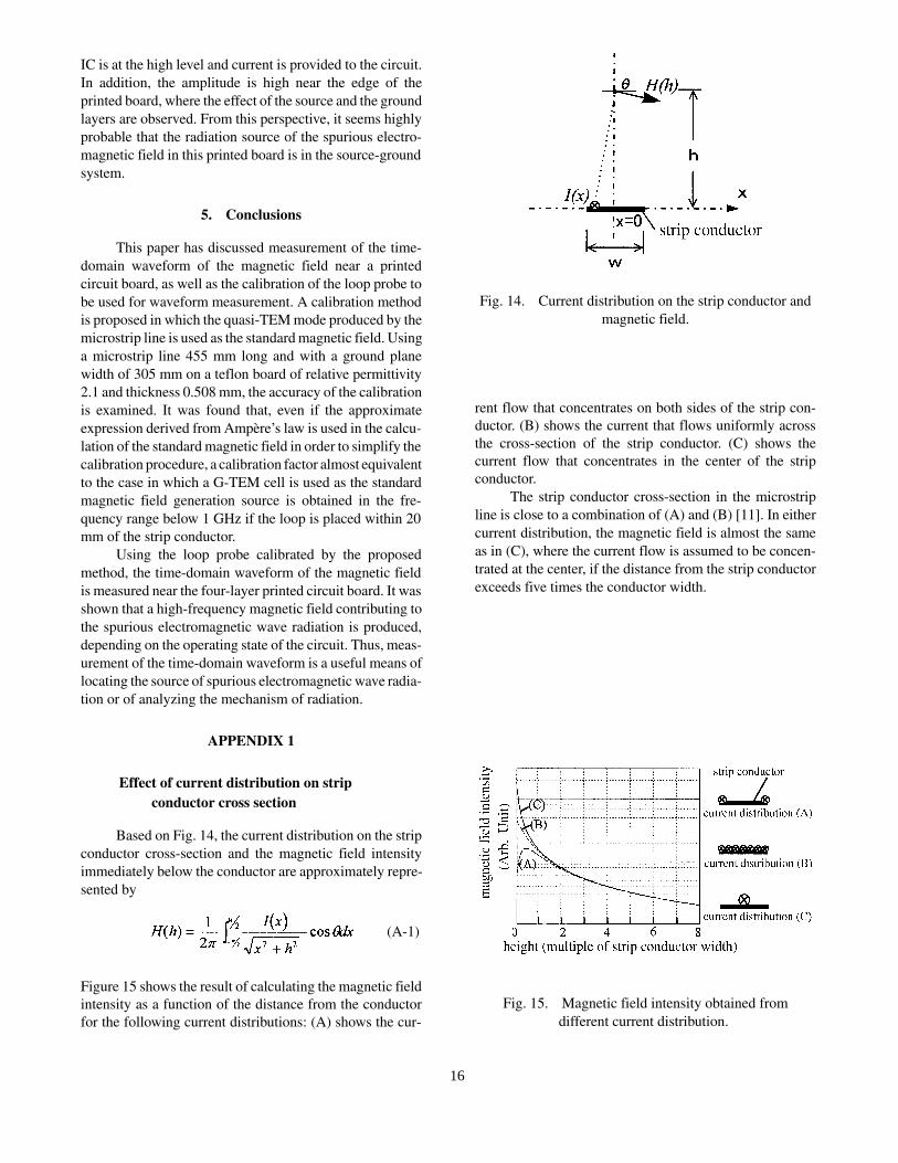
APPENDIX 1
Effect of current distribution on strip
conductor cross section
Based on Fig. 14, the current distribution on the strip
conductor cross-section and the magnetic field intensity
immediately below the conductor are approximately repre-
sented by
Figure 15 shows the result of calculating the magnetic field
intensity as a function of the distance from the conductor
for the following current distributions: (A) shows the cur-
rent flow that concentrates on both sides of the strip con-
ductor. (B) shows the current that flows uniformly across
the cross-section of the strip conductor. (C) shows the
current flow that concentrates in the center of the strip
conductor.
The strip conductor cross-section in the microstrip
line is close to a combination of (A) and (B) [11]. In either
current distribution, the magnetic field is almost the same
as in (C), where the current flow is assumed to be concen-
trated at the center, if the distance from the strip conductor
exceeds five times the conductor width.
Fig. 14. Current distribution on the strip conductor and
magnetic field.
Fig. 15. Magnetic field intensity obtained from
different current distribution.
(A-1)
16
APPENDIX 2
Derivation of calibration factor by S21
measurement
The calibration factor F.(w) is defined as the ratio of
the received magnetic field intensity H.(w) to the sensor
output voltage V.(w).
Substituting Eq. (7) into H.(w) of Eq. (A-2),
Since the terminal of the microstrip line is matched,
the current I.(w) is represented by the output V
.1(w) of the
network analyzer and the characteristic impedance 50 W of
the line:
The output is zero at port 2 of the network analyzer, and
port 1 is reflectionless. Thus, the ratio of the input voltage
V.(w) to the output voltage V
.1(w) of the port 1 is equal to
S.
21(w). Consequently,
The amplitude of the calibration factor F.(w) is
The phase of the measured S.
21(w) contains the phase delay
to the center of the line, the point used in the calibration.
The phase delay q(w) of the entire line is determined
beforehand by measurement and the phase at the center of
the line is q(w) / 2. Consequently, by correcting this term,
the phase of the sensor factor ÐF.(w) is given by
REFERENCES
1. T. Kurouchi, A. Ohneda, and A. Kami. A study of
noise sensing technique in small regions. Tech. Rep.
I.E.I.C.E., Vol. EMCJ94-12 (1994).
2. H. Sugama. A study of sensor for radiated electro-
magnetic noise measurement near electronic circuit.
Spr. Nat. Conv. I.E.I.C.E., B-271 (1995).
3. T. Harada and H. Sasaki. Spurious electromagnetic
wave radiation characteristics near multi-layer
printed circuit board. Tech. Rep. I.E.I.C.E., Vol.
EMCJ 96-13 (1996).
4. H. Sasaki and T. Harada. Time-domain waveform
measurement for high-frequency magnetic field near
printed circuit board. Tech. Rep. IEEJ, Vol. MAG-96-
48 (1996).
5. H. Sasaki and T. Harada. Estimation of spurious
electromagnetic radiation source by waveform meas-
urement of magnetic field near circuit. Nat. Conv.
I.E.I.C.E.J., B-275 (1996).
6. S. Iwasaki and S. Ishigami. Time-domain measure-
ment of ESD. 31st Elect. Comm. Lab. Symp. Electric
Discharge and EMC, pp. 87�94 (1994).
7. H. Sasaki, T. Harada, and E. Hankui. Calibration of
loop probe for magnetic field measurement. Nat.
Conv. I.E.I.C.E.J., B-285 (1994).
8. R. Middelkoop. Time-domain calibration of field
sensors for EMP measurements. IEEE Trans. Instru-
mentation and Measurement, Vol. IM-40, pp. 455�
459 (1991).
9. J.D. Hunter. The average axial magnetic field of a
loop antenna. IEEE Trans. Instrumentation and
Measurement, Vol. IM-24, pp. 261�263 (1975).
10. R. Itsukida, S. Ishigami, and S. Iwasaki. Application
of complex antenna factor to near field. Tech. Rep.
I.E.I.C.E., Vol. EMCJ 94-36 (1994).
(A-2)
(A-3)
(A-4)
(A-5)
(A-6)
(A-7)
17
AUTHORS (from left to right)
Takashi Harada (member) completed M.S. program (Electrical Eng.) at Tokyo Metropol. Univ. in 1983. Joined NEC Corp.
Apr. 1983. Engaged in development of electromagnetic wave absorber and shield materials, as well as research on suppression
of radiation from printed circuit boards. Now, with NEC Resource Environmental Technology Lab., EMC Technical Center.
Member, IEICEJ, Circuit Implementation Soc., Society for Applied Magnetism, and IEEE.
Hideki Sasaki (member) graduated Mar. 1991 from Nihon Univ. Completed 1st half of doctoral program (Electronic Eng.)
Mar. 1993. Joined NEC Corp. Apr. 1993. Mostly engaged in research on electromagnetic field measurement techniques.
Presently, with NEC Resource Environm. Tech. Lab., EMC Tech. Center. Presentation Award 1995 IEEJ. Member, IEICEJ.
Eiji Hankui (nonmember) graduated Mar. 1988 from Tokai Univ. Completed 1st half of doctoral program (Electrical Eng.)
Mar. 1990. Joined NEC Corp Apr. 1990. Mostly engaged in research on electromagnetic field measurement techniques and
effect of electromagnetics wave on man. Now with NEC Resource Environm. Tech. Lab. EMC Tech. Center. Member, IEICEJ,
Japan Society for Hyperthermal Oncology, and IEEE.
18