Embed Size (px)
Citation preview

RIGHT:
URL:
CITATION:
AUTHOR(S):
ISSUE DATE:
TITLE:
Resistive switching effects in singlemetallic tunneling junction withnanometer-scale gap
Mizukami, Takahiro; Miyato, Yuji; Kobayashi, Kei;Matsushige, Kazumi; Yamada, Hirofumi
Mizukami, Takahiro ...[et al]. Resistive switching effects in single metallic tunnelingjunction with nanometer-scale gap. APPLIED PHYSICS LETTERS 2011, 98(8): 083120.
2011-02
http://hdl.handle.net/2433/160628
Copyright 2011 American Institute of Physics. This article may be downloaded forpersonal use only. Any other use requires prior permission of the author and theAmerican Institute of Physics. The following article appeared in APPLIED PHYSICSLETTERS 98, 083120 (2011) and may be found at http://link.aip.org/link/?apl/98/083120

Resistive switching effects in single metallic tunneling junction withnanometer-scale gapTakahiro Mizukami, Yuji Miyato, Kei Kobayashi, Kazumi Matsushige, and Hirofumi Yamada Citation: Appl. Phys. Lett. 98, 083120 (2011); doi: 10.1063/1.3559612 View online: http://dx.doi.org/10.1063/1.3559612 View Table of Contents: http://apl.aip.org/resource/1/APPLAB/v98/i8 Published by the American Institute of Physics. Related ArticlesPinned interface dipole-induced tunneling electroresistance in ferroelectric tunnel junctions: A theoreticalinvestigation J. Appl. Phys. 112, 054104 (2012) Current-voltage characteristics and ON/OFF ratio in ferroelectric tunnel junctions J. Appl. Phys. 112, 054102 (2012) Observation of fluctuation-induced tunneling conduction in micrometer-sized tunnel junctions AIP Advances 2, 032155 (2012) Conductivity mapping of nanoparticles by torsional resonance tunneling atomic force microscopy Appl. Phys. Lett. 101, 083107 (2012) Zero-bias anomaly in one-dimensional ultrathin metallic nanowires AIP Advances 2, 032143 (2012) Additional information on Appl. Phys. Lett.Journal Homepage: http://apl.aip.org/ Journal Information: http://apl.aip.org/about/about_the_journal Top downloads: http://apl.aip.org/features/most_downloaded Information for Authors: http://apl.aip.org/authors
Downloaded 11 Sep 2012 to 130.54.110.73. Redistribution subject to AIP license or copyright; see http://apl.aip.org/about/rights_and_permissions
A Self-archived copy inKyoto University Research Information Repository
https://repository.kulib.kyoto-u.ac.jp
Resistive switching effects in single metallic tunneling junctionwith nanometer-scale gap
Takahiro Mizukami,1 Yuji Miyato,1 Kei Kobayashi,2 Kazumi Matsushige,1 andHirofumi Yamada1,a�
1Department of Electronic Science and Engineering, Kyoto University, Katsura, Nishikyo,Kyoto 615-8510, Japan2Office of Society-Academia Collaboration for Innovation, Kyoto University, Katsura, Nishikyo,Kyoto 615-8520, Japan
�Received 5 January 2011; accepted 4 February 2011; published online 25 February 2011�
We fabricated a single tunneling junction with a nanometer-scale gap between Pt electrodes. Wefound that the gap distance became smaller after a current sweep, which was presumably caused bythe migration of the Pt atoms at the anode. The junction showed a reproducible negative differentialresistance characteristic after reduction in the gap. The junction also showed resistive switchingcharacteristics with a resistance ratio of over 100 by applying voltage of different waveforms. Thetunneling area and gap distance for on/off-state were quantitatively estimated by fitting themeasured characteristics to the simple model as 100 nm2 and 0.8/1.2 nm, respectively. © 2011American Institute of Physics. �doi:10.1063/1.3559612�
A wide variety of resistive switching devices are cur-rently proposed for future nonvolatile memory systems. Theyinclude such as calcogenide phase-change memory devices,1
resistive random access memory based on metal oxide,2
atomic switches of the ionic salts,3,4 and molecularswitches.5
For the realization of ultrahigh density memory devices,the structure of the individual memory cell should be assimple as possible. Recently, Naitoh and co-workers6–10 re-ported a negative differential resistance �NDR� characteris-tics in metallic electrode junctions with a nanometer-scalegap. They also found that the current-voltage �I-V� curves ofthose nanoscale-gap junctions �NGJs� exhibit nonvolatile re-sistance switching phenomena even though the NGJs do nothave any memristive medium between electrodes. Theyfound a large change in the resistance with a ratio of up to105 depending on the waveform of the applied voltage,which was explained by the change in the gap distance be-tween the electrodes. The resistive switching occurs on Pd,Pt, and Ta electrodes as well as Au electrodes.8 Furthermore,it is also observed in the NGJs made of silicon electrodes,which demonstrates that the NGJ is compatible with semi-conductor process.9 Therefore, the NGJ is expected as abuilding block of the next-generation memory systems.However, the NDR characteristics and switching phenomenahave only been observed on the NGJs with relatively wideelectrode pairs which may contain multiple junctions untilrecently.10 Suga et al.10 recently reported that the NGJ madeby controlled break of a 45-nm-width nanowire also showsNDR characteristics and switching phenomena. However,they found that the active tunneling area in the device is stillwide and the electron tunneling is occurring at multiple sites.It would be important to fabricate narrower and thinner NGJso that the electron tunneling occurs at a single asperity forelucidation of the switching mechanisms of the NGJ andfrom the viewpoint of the reduction in the operating currentand miniaturization of the device as well.
In this study, we fabricated a single tunneling junctionwith a nanometer-scale gap between Pt electrodes by anelectron-beam �EB� lithography process, and investigatedelectrical properties, resistive switching characteristics, andstructural changes around the gap between electrodes byatomic force microscopy �AFM�.
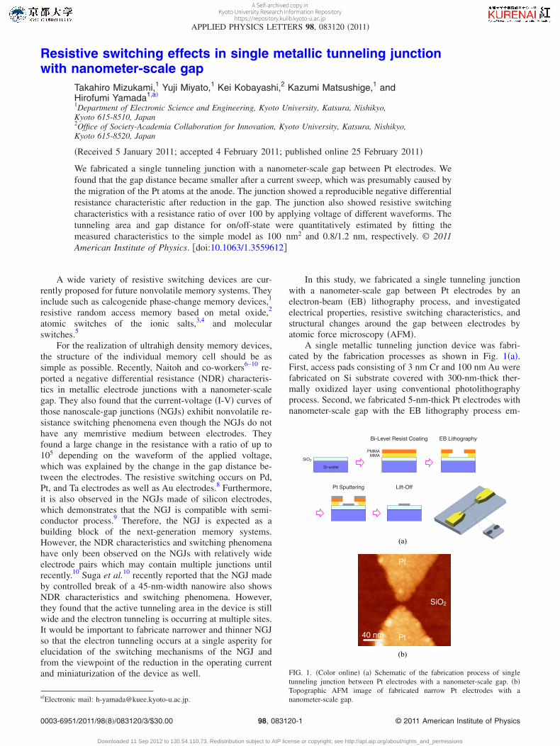
A single metallic tunneling junction device was fabri-cated by the fabrication processes as shown in Fig. 1�a�.First, access pads consisting of 3 nm Cr and 100 nm Au werefabricated on Si substrate covered with 300-nm-thick ther-mally oxidized layer using conventional photolithographyprocess. Second, we fabricated 5-nm-thick Pt electrodes withnanometer-scale gap with the EB lithography process em-
a�Electronic mail: [email protected].
40 nm
Pt
Pt
SiO2
PMMAMMA
Si-waferSiO2
Pt Sputtering Lift-Off
Bi-Level Resist Coating EB Lithography
(a)
(b)
FIG. 1. �Color online� �a� Schematic of the fabrication process of singletunneling junction between Pt electrodes with a nanometer-scale gap. �b�Topographic AFM image of fabricated narrow Pt electrodes with ananometer-scale gap.
APPLIED PHYSICS LETTERS 98, 083120 �2011�
0003-6951/2011/98�8�/083120/3/$30.00 © 2011 American Institute of Physics98, 083120-1
Downloaded 11 Sep 2012 to 130.54.110.73. Redistribution subject to AIP license or copyright; see http://apl.aip.org/about/rights_and_permissions
A Self-archived copy inKyoto University Research Information Repository
https://repository.kulib.kyoto-u.ac.jp
ploying a bilayer resist film. We spun methyl methacrylate�MMA� film as a bottom layer, and poly-MMA �PMMA�film as a top layer. After baking the resist film, electrodeswith a nanometer-scale gap were defined between the Au/Craccess pads by the EB. After development, an overhangstructure was obtained because MMA dissolves faster thanPMMA, which prevents ragged edge formation after lift-offprocess. We deposited ultrathin Pt film with a thickness of5 nm by rf sputtering. We employed Pt for this study sincewe already established ultrathin and continuous Pt film by rfsputtering.11 Finally the resist film was lifted off by agitationin removing agent �Microposit: Remover 1165�.
Figure 1�b� shows a topographic AFM image taken onthe area around the electrode gap of a fabricated NGJ device.We used a commercially available AFM instrument �JEOL:JSPM-5200� and a Si cantilever �Olympus: OMCL-AC160�whose nominal spring constant and resonance frequencywere 42 N/m and 300 kHz, respectively. The image wastaken with the intermittent contact mode. The gap distancebetween electrodes measured from the cross-sectional lineprofile of the image was about 5 nm, which might be slightlysmaller than the actual gap distance because the tip radiuswas about 5 nm.
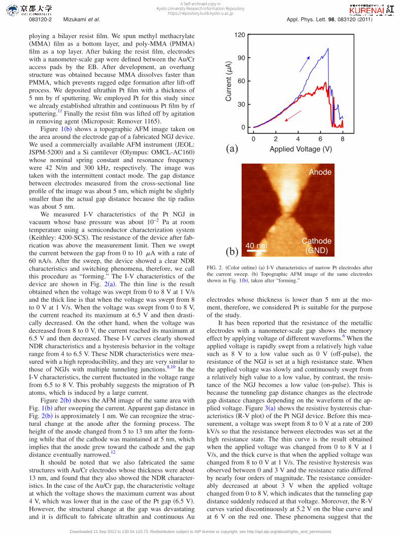
We measured I-V characteristics of the Pt NGJ invacuum whose base pressure was about 10−2 Pa at roomtemperature using a semiconductor characterization system�Keithley: 4200-SCS�. The resistance of the device after fab-rication was above the measurement limit. Then we sweptthe current between the gap from 0 to 10 �A with a rate of60 nA/s. After the sweep, the device showed a clear NDRcharacteristics and switching phenomena, therefore, we callthis procedure as “forming.” The I-V characteristics of thedevice are shown in Fig. 2�a�. The thin line is the resultobtained when the voltage was swept from 0 to 8 V at 1 V/sand the thick line is that when the voltage was swept from 8to 0 V at 1 V/s. When the voltage was swept from 0 to 8 V,the current reached its maximum at 6.5 V and then drasti-cally decreased. On the other hand, when the voltage wasdecreased from 8 to 0 V, the current reached its maximum at6.5 V and then decreased. These I-V curves clearly showedNDR characteristics and a hysteresis behavior in the voltagerange from 4 to 6.5 V. These NDR characteristics were mea-sured with a high reproducibility, and they are very similar tothose of NGJs with multiple tunneling junctions.8,10 In theI-V characteristics, the current fluctuated in the voltage rangefrom 6.5 to 8 V. This probably suggests the migration of Ptatoms, which is induced by a large current.
Figure 2�b� shows the AFM image of the same area withFig. 1�b� after sweeping the current. Apparent gap distance inFig. 2�b� is approximately 1 nm. We can recognize the struc-tural change at the anode after the forming process. Theheight of the anode changed from 5 to 13 nm after the form-ing while that of the cathode was maintained at 5 nm, whichimplies that the anode grew toward the cathode and the gapdistance eventually narrowed.12
It should be noted that we also fabricated the samestructures with Au/Cr electrodes whose thickness were about13 nm, and found that they also showed the NDR character-istics. In the case of the Au/Cr gap, the characteristic voltageat which the voltage shows the maximum current was about4 V, which was lower that in the case of the Pt gap �6.5 V�.However, the structural change at the gap was devastatingand it is difficult to fabricate ultrathin and continuous Au
electrodes whose thickness is lower than 5 nm at the mo-ment, therefore, we considered Pt is suitable for the purposeof the study.
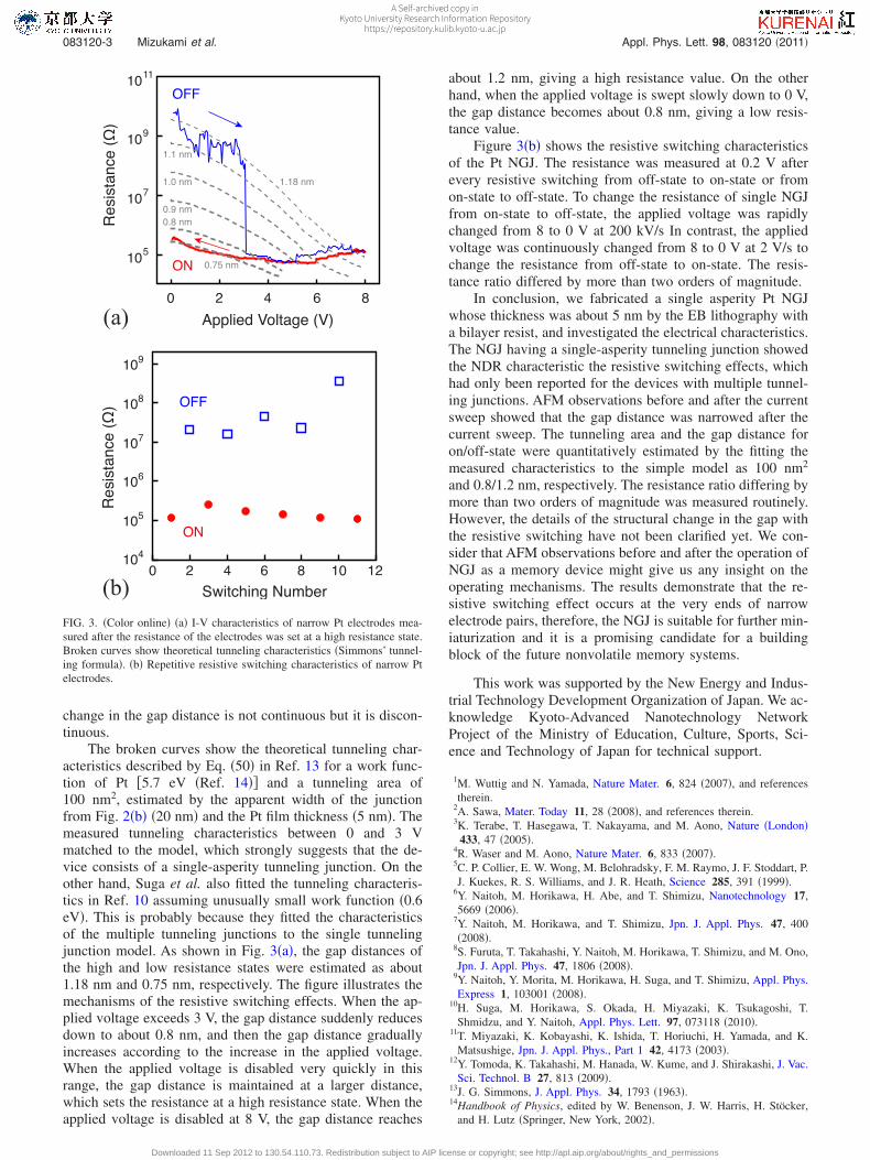
It has been reported that the resistance of the metallicelectrodes with a nanometer-scale gap shows the memoryeffect by applying voltage of different waveforms.6 When theapplied voltage is rapidly swept from a relatively high valuesuch as 8 V to a low value such as 0 V �off-pulse�, theresistance of the NGJ is set at a high resistance state. Whenthe applied voltage was slowly and continuously swept froma relatively high value to a low value, by contrast, the resis-tance of the NGJ becomes a low value �on-pulse�. This isbecause the tunneling gap distance changes as the electrodegap distance changes depending on the waveform of the ap-plied voltage. Figure 3�a� shows the resistive hysteresis char-acteristics �R-V plot� of the Pt NGJ device. Before this mea-surement, a voltage was swept from 8 to 0 V at a rate of 200kV/s so that the resistance between electrodes was set at thehigh resistance state. The thin curve is the result obtainedwhen the applied voltage was changed from 0 to 8 V at 1V/s, and the thick curve is that when the applied voltage waschanged from 8 to 0 V at 1 V/s. The resistive hysteresis wasobserved between 0 and 3 V and the resistance ratio differedby nearly four orders of magnitude. The resistance consider-ably decreased at about 3 V when the applied voltagechanged from 0 to 8 V, which indicates that the tunneling gapdistance suddenly reduced at that voltage. Moreover, the R-Vcurves varied discontinuously at 5.2 V on the blue curve andat 6 V on the red one. These phenomena suggest that the
(b) 40 nm
Anode
Cathode(GND)
0
30
60
90
120
Current(μA)
0 2 4 6 8Applied Voltage (V)(a)
FIG. 2. �Color online� �a� I-V characteristics of narrow Pt electrodes afterthe current sweep. �b� Topographic AFM image of the same electrodesshown in Fig. 1�b�, taken after “forming.”
083120-2 Mizukami et al. Appl. Phys. Lett. 98, 083120 �2011�
Downloaded 11 Sep 2012 to 130.54.110.73. Redistribution subject to AIP license or copyright; see http://apl.aip.org/about/rights_and_permissions
A Self-archived copy inKyoto University Research Information Repository
https://repository.kulib.kyoto-u.ac.jp
change in the gap distance is not continuous but it is discon-tinuous.
The broken curves show the theoretical tunneling char-acteristics described by Eq. �50� in Ref. 13 for a work func-tion of Pt �5.7 eV �Ref. 14�� and a tunneling area of100 nm2, estimated by the apparent width of the junctionfrom Fig. 2�b� �20 nm� and the Pt film thickness �5 nm�. Themeasured tunneling characteristics between 0 and 3 Vmatched to the model, which strongly suggests that the de-vice consists of a single-asperity tunneling junction. On theother hand, Suga et al. also fitted the tunneling characteris-tics in Ref. 10 assuming unusually small work function �0.6eV�. This is probably because they fitted the characteristicsof the multiple tunneling junctions to the single tunnelingjunction model. As shown in Fig. 3�a�, the gap distances ofthe high and low resistance states were estimated as about1.18 nm and 0.75 nm, respectively. The figure illustrates themechanisms of the resistive switching effects. When the ap-plied voltage exceeds 3 V, the gap distance suddenly reducesdown to about 0.8 nm, and then the gap distance graduallyincreases according to the increase in the applied voltage.When the applied voltage is disabled very quickly in thisrange, the gap distance is maintained at a larger distance,which sets the resistance at a high resistance state. When theapplied voltage is disabled at 8 V, the gap distance reaches
about 1.2 nm, giving a high resistance value. On the otherhand, when the applied voltage is swept slowly down to 0 V,the gap distance becomes about 0.8 nm, giving a low resis-tance value.
Figure 3�b� shows the resistive switching characteristicsof the Pt NGJ. The resistance was measured at 0.2 V afterevery resistive switching from off-state to on-state or fromon-state to off-state. To change the resistance of single NGJfrom on-state to off-state, the applied voltage was rapidlychanged from 8 to 0 V at 200 kV/s In contrast, the appliedvoltage was continuously changed from 8 to 0 V at 2 V/s tochange the resistance from off-state to on-state. The resis-tance ratio differed by more than two orders of magnitude.
In conclusion, we fabricated a single asperity Pt NGJwhose thickness was about 5 nm by the EB lithography witha bilayer resist, and investigated the electrical characteristics.The NGJ having a single-asperity tunneling junction showedthe NDR characteristic the resistive switching effects, whichhad only been reported for the devices with multiple tunnel-ing junctions. AFM observations before and after the currentsweep showed that the gap distance was narrowed after thecurrent sweep. The tunneling area and the gap distance foron/off-state were quantitatively estimated by the fitting themeasured characteristics to the simple model as 100 nm2
and 0.8/1.2 nm, respectively. The resistance ratio differing bymore than two orders of magnitude was measured routinely.However, the details of the structural change in the gap withthe resistive switching have not been clarified yet. We con-sider that AFM observations before and after the operation ofNGJ as a memory device might give us any insight on theoperating mechanisms. The results demonstrate that the re-sistive switching effect occurs at the very ends of narrowelectrode pairs, therefore, the NGJ is suitable for further min-iaturization and it is a promising candidate for a buildingblock of the future nonvolatile memory systems.
This work was supported by the New Energy and Indus-trial Technology Development Organization of Japan. We ac-knowledge Kyoto-Advanced Nanotechnology NetworkProject of the Ministry of Education, Culture, Sports, Sci-ence and Technology of Japan for technical support.
1M. Wuttig and N. Yamada, Nature Mater. 6, 824 �2007�, and referencestherein.
2A. Sawa, Mater. Today 11, 28 �2008�, and references therein.3K. Terabe, T. Hasegawa, T. Nakayama, and M. Aono, Nature �London�
433, 47 �2005�.4R. Waser and M. Aono, Nature Mater. 6, 833 �2007�.5C. P. Collier, E. W. Wong, M. Belohradsky, F. M. Raymo, J. F. Stoddart, P.J. Kuekes, R. S. Williams, and J. R. Heath, Science 285, 391 �1999�.
6Y. Naitoh, M. Horikawa, H. Abe, and T. Shimizu, Nanotechnology 17,5669 �2006�.
7Y. Naitoh, M. Horikawa, and T. Shimizu, Jpn. J. Appl. Phys. 47, 400�2008�.
8S. Furuta, T. Takahashi, Y. Naitoh, M. Horikawa, T. Shimizu, and M. Ono,Jpn. J. Appl. Phys. 47, 1806 �2008�.
9Y. Naitoh, Y. Morita, M. Horikawa, H. Suga, and T. Shimizu, Appl. Phys.Express 1, 103001 �2008�.
10H. Suga, M. Horikawa, S. Okada, H. Miyazaki, K. Tsukagoshi, T.Shmidzu, and Y. Naitoh, Appl. Phys. Lett. 97, 073118 �2010�.
11T. Miyazaki, K. Kobayashi, K. Ishida, T. Horiuchi, H. Yamada, and K.Matsushige, Jpn. J. Appl. Phys., Part 1 42, 4173 �2003�.
12Y. Tomoda, K. Takahashi, M. Hanada, W. Kume, and J. Shirakashi, J. Vac.Sci. Technol. B 27, 813 �2009�.
13J. G. Simmons, J. Appl. Phys. 34, 1793 �1963�.14Handbook of Physics, edited by W. Benenson, J. W. Harris, H. Stöcker,
and H. Lutz �Springer, New York, 2002�.
2 4 6 8 10 12Switching Number
0104
105
106
107
108
109
Resistance(Ω) OFF
ON
(b)
0.75 nm
1.0 nm 1.18 nm
0.9 nm0.8 nm
1.1 nm
0 2 4 6 8Applied Voltage (V)
10
10
10
10
5
7
9
11
Resistance(Ω)
OFF
ON
(a)
FIG. 3. �Color online� �a� I-V characteristics of narrow Pt electrodes mea-sured after the resistance of the electrodes was set at a high resistance state.Broken curves show theoretical tunneling characteristics �Simmons’ tunnel-ing formula�. �b� Repetitive resistive switching characteristics of narrow Ptelectrodes.
083120-3 Mizukami et al. Appl. Phys. Lett. 98, 083120 �2011�
Downloaded 11 Sep 2012 to 130.54.110.73. Redistribution subject to AIP license or copyright; see http://apl.aip.org/about/rights_and_permissions
A Self-archived copy inKyoto University Research Information Repository
https://repository.kulib.kyoto-u.ac.jp