Embed Size (px)
Citation preview

TLV1117-ADJOUTPUT
ADJ/GND
INPUT
Product
Folder
Sample &Buy
Technical
Documents
Tools &
Software
Support &Community
TLV1117SLVS561L –DECEMBER 2004–REVISED OCTOBER 2014
TLV1117 Adjustable and Fixed Low-Dropout Voltage Regulator1 Features 3 Description
The TLV1117 device is a positive low-dropout voltage1• 1.5-V, 1.8-V, 2.5-V, 3.3-V, 5-V, and
regulator designed to provide up to 800 mA of outputAdjustable-Output Voltage Optionscurrent. The device is available in 1.5-V, 1.8-V, 2.5-V,
• Output Current of 800 mA 3.3-V, 5-V, and adjustable-output voltage options. All• Specified Dropout Voltage at Multiple internal circuitry is designed to operate down to 1-V
input-to-output differential. Dropout voltage isCurrent Levelsspecified at a maximum of 1.3 V at 800 mA,• 0.2% Line Regulation Maximumdecreasing at lower load currents.
• 0.4% Load Regulation MaximumDevice Information
2 Applications ORDER NUMBER PACKAGE (PIN) BODY SIZE• Electronic Points of Sale TLV1117DCY SOT-223 (4) 6.50 mm × 3.50 mm• Medical, Health, and Fitness Applications TLV1117DRJ SON (8) 4.00 mm × 4.00 mm
TLV1117KVU TO-252 (3) 6.60 mm × 6.10 mm• PrintersTLV1117KCS TO-220 (3) 10.16 mm × 8.70 mm• Appliances and White GoodsTLV1117KCT TO-220 (3) 10.16 mm × 8.59 mm• TV Set-Top Boxes
DDPAK,TLV1117KTT 10.18 mm × 8.41 mmTO-263 (3)
4 Simplified Schematic
1
An IMPORTANT NOTICE at the end of this data sheet addresses availability, warranty, changes, use in safety-critical applications,intellectual property matters and other important disclaimers. PRODUCTION DATA.

TLV1117SLVS561L –DECEMBER 2004–REVISED OCTOBER 2014 www.ti.com
Table of Contents8.1 Overview ................................................................. 101 Features .................................................................. 18.2 Functional Block Diagram ....................................... 102 Applications ........................................................... 18.3 Feature Description................................................. 103 Description ............................................................. 18.4 Device Functional Modes........................................ 104 Simplified Schematic............................................. 1
9 Application and Implementation ........................ 125 Revision History..................................................... 29.1 Typical Application ................................................. 126 Pin Configuration and Functions ......................... 3
10 Power Supply Recommendations ..................... 137 Specifications......................................................... 411 Layout................................................................... 137.1 Absolute Maximum Ratings ..................................... 4
11.1 Layout Guidelines ................................................. 137.2 Handling Ratings ...................................................... 411.2 Layout Example .................................................... 137.3 Recommended Operating Conditions....................... 4
12 Device and Documentation Support ................. 147.4 Thermal Information .................................................. 512.1 Trademarks ........................................................... 147.5 TLV1117C Electrical Characteristics ........................ 612.2 Electrostatic Discharge Caution............................ 147.6 TLV1117I Electrical Characteristics .......................... 712.3 Glossary ................................................................ 147.7 Typical Characteristics .............................................. 8
13 Mechanical, Packaging, and Orderable8 Detailed Description ............................................ 10Information ........................................................... 14
Changes from Revision K (April 2013) to Revision L Page
• Updated data sheet to new TI standards – no specification changes. .................................................................................. 1• Deleted Ordering Information table. ...................................................................................................................................... 1• Added Applications. ................................................................................................................................................................ 1• Added Device and Documentation Support section............................................................................................................. 14• Added Mechanical, Packaging, and Orderable Information section..................................................................................... 14
5 Revision History
Changes from Revision J (April 2013) to Revision K Page
• Added additional package options.......................................................................................................................................... 3• Added ESD warning. ............................................................................................................................................................ 14
2 Submit Documentation Feedback Copyright © 2004–2014, Texas Instruments Incorporated
Product Folder Links: TLV1117

INPUT
OUTPUT
ADJ/GND
OU
TP
UT
DCY (SOT-223) PACKAGE(TOP VIEW)
VOUT(2)
ADJ/GND
2
3
4
1 8
7
6
5
VIN(1)
VIN(1)
VIN(1)
VOUT(2)
VOUT(2)
NC
(1) VIN pins (2, 3, 4) must be connected together.
(2) VOUT pins (5, 6, 7) must be connected together.
VOUT
DRJ (QFN) PACKAGE(TOP VIEW)
OUTPUTINPUT
ADJ/GND
OU
TP
UT
KCT, KCS (TO-220) PACKAGE(TOP VIEW)
3
2
1
321
INPUT
OUTPUT
ADJ/GNDOU
TP
UT
KTT (TO-263) PACKAGE(TOP VIEW)
OUTPUT
INPUT
ADJ/GND
OU
TP
UT
KVU (TO-252) PACKAGE(TOP VIEW)
3
2
1
3
2
1
TLV1117www.ti.com SLVS561L –DECEMBER 2004–REVISED OCTOBER 2014
6 Pin Configuration and Functions
Table 1. Pin FunctionsPIN
TYPE DESCRIPTIONNAME KTT KVU DCY DRJ KCTADJ/GND 1 1 1 1 1 I/O Output voltage adjustment pin. Connect to a resistor divider.INPUT 3 3 3 2, 3, 4 3 I Voltage inputOUTPUT 2 2 2 5, 6, 7 2 O Voltage outputNC - - - 8 - - No connect
Copyright © 2004–2014, Texas Instruments Incorporated Submit Documentation Feedback 3
Product Folder Links: TLV1117

TLV1117SLVS561L –DECEMBER 2004–REVISED OCTOBER 2014 www.ti.com
7 Specifications
7.1 Absolute Maximum Ratings (1)
over operating free-air temperature range (unless otherwise noted)MIN MAX UNIT
VIN Continuous input voltage 16 VTJ Operating virtual-junction temperature 150 °C
(1) Stresses beyond those listed under Absolute Maximum Ratings may cause permanent damage to the device. These are stress ratingsonly, and functional operation of the device at these or any other conditions beyond those indicated under Recommended OperatingConditions is not implied. Exposure to absolute-maximum-rated conditions for extended periods may affect device reliability.
7.2 Handling RatingsMIN MAX UNIT
Tstg Storage temperature range –65 150 °CHuman body model (HBM), per ANSI/ESDA/JEDEC JS-001, all 0 2500pins (1)
V(ESD) Electrostatic discharge VCharged device model (CDM), per JEDEC specification 0 1500JESD22-C101, all pins (2)
(1) JEDEC document JEP155 states that 500-V HBM allows safe manufacturing with a standard ESD control process.(2) JEDEC document JEP157 states that 250-V CDM allows safe manufacturing with a standard ESD control process.
7.3 Recommended Operating ConditionsMIN (1) MAX UNIT
TLV1117 2.7 15TLV1117-15 2.9 15TLV1117-18 3.2 15
VIN Input voltage VTLV1117-25 3.9 15TLV1117-33 4.7 15TLV1117-50 6.4 15
IO Output current 0.8 ATLV1117C 0 125
TJ Operating virtual-junction temperature °CTLV1117I –40 125
(1) The input-to-output differential across the regulator should provide for some margin against regulator operation at the maximum dropout(for a particular current value). This margin is needed to account for tolerances in both the input voltage (lower limit) and the outputvoltage (upper limit). The absolute minimum VIN for a desired maximum output current can be calculated by the following:VIN(min) = VOUT(max) + VDO(max at rated current)
4 Submit Documentation Feedback Copyright © 2004–2014, Texas Instruments Incorporated
Product Folder Links: TLV1117

TLV1117www.ti.com SLVS561L –DECEMBER 2004–REVISED OCTOBER 2014
7.4 Thermal InformationTLV1117
PowerFlexTHERMAL METRIC (1) (2) (3) UNITSKTE KTP DRJ DCY KVU KCS, KCT KTT
(3 PINS) (3 PINS) (8 PINS) (4 PINS) (3 PINS) (3 PINS) (3 PINS)Junction-to-ambient thermalRθJA 38.6 49.2 38.3 104.3 50.9 30.1 27.5resistanceJunction-to-case (top) thermalRθJC(top) 34.7 60.6 36.5 53.7 57.9 44.6 43.2resistance
RθJB Junction-to-board thermal resistance 3.2 3.1 60.5 5.7 34.8 1.2 17.3Junction-to-top characterizationψJT 5.9 8.7 0.2 3.1 6 5 2.8parameter °C/WJunction-to-board characterizationψJB 3.1 3 12 5.5 23.7 1.2 9.3parameterJunction-to-case (bottom) thermalRθJC(bot) 3 3 4.7 n/a 0.4 0.4 0.3resistanceThermal resistance between the die
RθJP junction and the bottom of the 2.7 1.4 1.78 n/a n/a 3 1.94exposed pad.
(1) For more information about traditional and new thermal metrics, see the IC Package Thermal Metrics application report, SPRA953.(2) For thermal estimates of this device based on PCB copper area, see the TI PCB Thermal Calculator.(3) Maximum power dissipation is a function of TJ(max), θJA, and TA. The maximum allowable power dissipation at any allowable ambient
temperature is PD = (TJ(max) – TA) / θJA. Operating at the absolute maximum TJ of 150°C can affect reliability.
Copyright © 2004–2014, Texas Instruments Incorporated Submit Documentation Feedback 5
Product Folder Links: TLV1117
TLV1117SLVS561L –DECEMBER 2004–REVISED OCTOBER 2014 www.ti.com
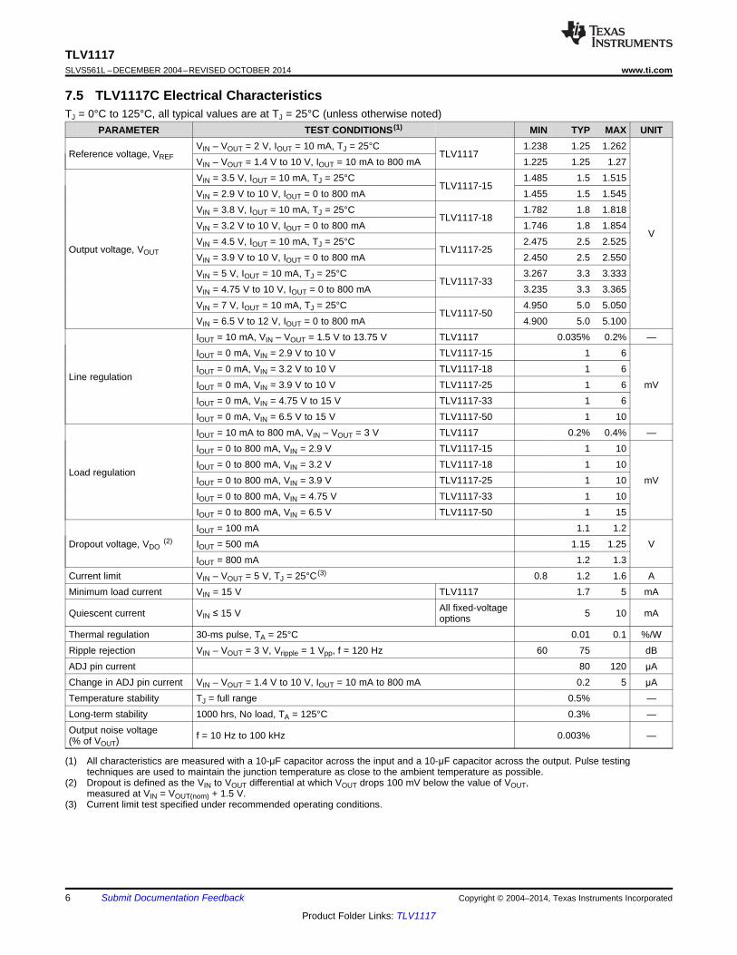
7.5 TLV1117C Electrical CharacteristicsTJ = 0°C to 125°C, all typical values are at TJ = 25°C (unless otherwise noted)
PARAMETER TEST CONDITIONS (1) MIN TYP MAX UNITVIN – VOUT = 2 V, IOUT = 10 mA, TJ = 25°C 1.238 1.25 1.262
Reference voltage, VREF TLV1117VIN – VOUT = 1.4 V to 10 V, IOUT = 10 mA to 800 mA 1.225 1.25 1.27VIN = 3.5 V, IOUT = 10 mA, TJ = 25°C 1.485 1.5 1.515
TLV1117-15VIN = 2.9 V to 10 V, IOUT = 0 to 800 mA 1.455 1.5 1.545VIN = 3.8 V, IOUT = 10 mA, TJ = 25°C 1.782 1.8 1.818
TLV1117-18VIN = 3.2 V to 10 V, IOUT = 0 to 800 mA 1.746 1.8 1.854
VVIN = 4.5 V, IOUT = 10 mA, TJ = 25°C 2.475 2.5 2.525
Output voltage, VOUT TLV1117-25VIN = 3.9 V to 10 V, IOUT = 0 to 800 mA 2.450 2.5 2.550VIN = 5 V, IOUT = 10 mA, TJ = 25°C 3.267 3.3 3.333
TLV1117-33VIN = 4.75 V to 10 V, IOUT = 0 to 800 mA 3.235 3.3 3.365VIN = 7 V, IOUT = 10 mA, TJ = 25°C 4.950 5.0 5.050
TLV1117-50VIN = 6.5 V to 12 V, IOUT = 0 to 800 mA 4.900 5.0 5.100IOUT = 10 mA, VIN – VOUT = 1.5 V to 13.75 V TLV1117 0.035% 0.2% —IOUT = 0 mA, VIN = 2.9 V to 10 V TLV1117-15 1 6IOUT = 0 mA, VIN = 3.2 V to 10 V TLV1117-18 1 6
Line regulationIOUT = 0 mA, VIN = 3.9 V to 10 V TLV1117-25 1 6 mVIOUT = 0 mA, VIN = 4.75 V to 15 V TLV1117-33 1 6IOUT = 0 mA, VIN = 6.5 V to 15 V TLV1117-50 1 10IOUT = 10 mA to 800 mA, VIN – VOUT = 3 V TLV1117 0.2% 0.4% —IOUT = 0 to 800 mA, VIN = 2.9 V TLV1117-15 1 10IOUT = 0 to 800 mA, VIN = 3.2 V TLV1117-18 1 10
Load regulationIOUT = 0 to 800 mA, VIN = 3.9 V TLV1117-25 1 10 mVIOUT = 0 to 800 mA, VIN = 4.75 V TLV1117-33 1 10IOUT = 0 to 800 mA, VIN = 6.5 V TLV1117-50 1 15IOUT = 100 mA 1.1 1.2
Dropout voltage, VDO(2) IOUT = 500 mA 1.15 1.25 V
IOUT = 800 mA 1.2 1.3Current limit VIN – VOUT = 5 V, TJ = 25°C (3) 0.8 1.2 1.6 AMinimum load current VIN = 15 V TLV1117 1.7 5 mA
All fixed-voltageQuiescent current VIN ≤ 15 V 5 10 mAoptionsThermal regulation 30-ms pulse, TA = 25°C 0.01 0.1 %/WRipple rejection VIN – VOUT = 3 V, Vripple = 1 Vpp, f = 120 Hz 60 75 dBADJ pin current 80 120 μAChange in ADJ pin current VIN – VOUT = 1.4 V to 10 V, IOUT = 10 mA to 800 mA 0.2 5 μATemperature stability TJ = full range 0.5% —Long-term stability 1000 hrs, No load, TA = 125°C 0.3% —Output noise voltage f = 10 Hz to 100 kHz 0.003% —(% of VOUT)
(1) All characteristics are measured with a 10-μF capacitor across the input and a 10-μF capacitor across the output. Pulse testingtechniques are used to maintain the junction temperature as close to the ambient temperature as possible.
(2) Dropout is defined as the VIN to VOUT differential at which VOUT drops 100 mV below the value of VOUT,measured at VIN = VOUT(nom) + 1.5 V.
(3) Current limit test specified under recommended operating conditions.
6 Submit Documentation Feedback Copyright © 2004–2014, Texas Instruments Incorporated
Product Folder Links: TLV1117

TLV1117www.ti.com SLVS561L –DECEMBER 2004–REVISED OCTOBER 2014
7.6 TLV1117I Electrical CharacteristicsTJ = –40°C to 125°C, all typical values are at TJ = 25°C (unless otherwise noted)
PARAMETER TEST CONDITIONS (1) MIN TYP MAX UNITVIN – VOUT = 2 V, IOUT = 10 mA, TJ = 25°C 1.238 1.25 1.262
Reference voltage, VREF TLV1117VIN – VOUT = 1.4 V to 10 V, IOUT = 10 mA to 800 mA 1.200 1.25 1.29VIN = 3.5 V, IOUT = 10 mA, TJ = 25°C 1.485 1.5 1.515
TLV1117-15VIN = 2.9 V to 10 V, IOUT = 0 to 800 mA 1.44 1.5 1.56VIN = 3.8 V, IOUT = 10 mA, TJ = 25°C 1.782 1.8 1.818
TLV1117-18VIN = 3.2 V to 10 V, IOUT = 0 to 800 mA 1.728 1.8 1.872
VVIN = 4.5 V, IOUT = 10 mA, TJ = 25°C 2.475 2.5 2.525
Output voltage, VOUT TLV1117-25VIN = 3.9 V to 10 V, IOUT = 0 to 800 mA 2.4 2.5 2.6VIN = 5 V, IOUT = 10 mA, TJ = 25°C 3.267 3.3 3.333
TLV1117-33VIN = 4.75 V to 10 V, IOUT = 0 to 800 mA 3.168 3.3 3.432VIN = 7 V, IOUT = 10 mA, TJ = 25°C 4.95 5.0 5.05
TLV1117-50VIN = 6.5 V to 12 V, IOUT = 0 to 800 mA 4.80 5.0 5.20IOUT = 10 mA, VIN – VOUT = 1.5 V to 13.75 V TLV1117 0.035% 0.3% —IOUT = 0 mA, VIN = 2.9 V to 10 V TLV1117-15 1 10IOUT = 0 mA, VIN = 3.2 V to 10 V TLV1117-18 1 10
Line regulationIOUT = 0 mA, VIN = 3.9 V to 10 V TLV1117-25 1 10 mVIOUT = 0 mA, VIN = 4.75 V to 15 V TLV1117-33 1 10IOUT = 0 mA, VIN = 6.5 V to 15 V TLV1117-50 1 15IOUT = 10 mA to 800 mA, VIN – VOUT = 3 V TLV1117 0.2% 0.5% —IOUT = 0 to 800 mA, VIN = 2.9 V TLV1117-15 1 15IOUT = 0 to 800 mA, VIN = 3.2 V TLV1117-18 1 15
Load regulationIOUT = 0 to 800 mA, VIN = 3.9 V TLV1117-25 1 15 mVIOUT = 0 to 800 mA, VIN = 4.75 V TLV1117-33 1 15IOUT = 0 to 800 mA, VIN = 6.5 V TLV1117-50 1 20IOUT = 100 mA 1.1 1.3
Dropout voltage, VDO(2) IOUT = 500 mA 1.15 1.35 V
IOUT = 800 mA 1.2 1.4Current limit VIN – VOUT = 5 V, TJ = 25°C (3) 0.8 1.2 1.6 AMinimum load current VIN = 15 V TLV1117 1.7 5 mA
All fixed-voltageQuiescent current VIN ≤ 15 V 5 15 mAoptionsThermal regulation 30-ms pulse, TA = 25°C 0.01 0.1 %/WRipple rejection VIN – VOUT = 3 V, Vripple = 1 Vpp, f = 120 Hz 60 75 dBADJ pin current 80 120 μAChange in ADJ pin current VIN – VOUT = 1.4 V to 10 V, IOUT = 10 mA to 800 mA 0.2 10 μATemperature stability TJ = full range 0.5% —Long-term stability 1000 hrs, No load, TA = 125°C 0.3% —Output noise voltage f = 10 Hz to 100 kHz 0.003% —(% of VOUT)
(1) All characteristics are measured with a 10-μF capacitor across the input and a 10-μF capacitor across the output. Pulse testingtechniques are used to maintain the junction temperature as close to the ambient temperature as possible.
(2) Dropout is defined as the VIN to VOUT differential at which VOUT drops 100 mV below the value of VOUT,measured at VIN = VOUT(nom) + 1.5 V.
(3) Current limit test specified under recommended operating conditions
Copyright © 2004–2014, Texas Instruments Incorporated Submit Documentation Feedback 7
Product Folder Links: TLV1117

−2
−1.5
−1
−0.5
0
0.5
1
1.5
2
Temperature ( C)
Out
put V
olta
ge V
aria
tion
(%)
1251007550250−25−50 15060
70
80
90
100
110
120
130
140
150
Temperature ( C)
AD
J P
in C
urre
nt (
A)
1251007550250−25−50 150
0
10
20
30
40
50
60
70
80
90
0 200 400 600 800
Load (mA)
Rip
ple
Rej
ectio
n (d
B)f = 120 Hz
0
10
20
30
40
50
60
70
80
Frequency (Hz)
Rip
ple
Rej
ectio
n (d
B)
100k10k1k10010
−0.35
−0.3
−0.25
−0.2
−0.15
−0.1
−0.05
0
Temperature ( C)
1251007550250−25−50
V
OU
T (%
)
Load = 800 mA
Input/Output Differential (V)
Sho
rt-C
ircu
it C
urre
nt (
A)
0
0.2
0.4
0.6
0.8
1
1.2
1.4
1.6
1.8
TJ = 25C
TJ = 125C
0 1512963
TLV1117SLVS561L –DECEMBER 2004–REVISED OCTOBER 2014 www.ti.com
7.7 Typical Characteristics
Figure 1. Short-Circuit Current vs (VIN – VOUT) Figure 2. Load Regulation
Figure 3. Ripple Rejection vs Frequency (ADJ Version) Figure 4. Ripple Rejection vs Load Current (ADJ Version)
Figure 5. Temperature Stability Figure 6. ADJ Pin Current vs Temperature
8 Submit Documentation Feedback Copyright © 2004–2014, Texas Instruments Incorporated
Product Folder Links: TLV1117

−20
−10
0
10
20
30
40
50
60
70
80
90
100
Time (s)
Out
put V
olta
ge D
evia
tion
(mV
)
1
2
3
4
5
6
7
Inpu
t Vol
tage
(V
)
CIN = 0.1 FCOUT = 10-F TantalumIOUT = 0.1 A
−40 −20 0 20 40 60 80 100 120 140
Input Voltage
Output-Voltage Deviation
−0.5
−0.4
−0.3
−0.2
−0.1
0
0.1
0.2
Time (s)
Out
put V
olta
ge D
evia
tion
(V)
−0.2
0
0.2
0.4
0.6
0.8
1
1.2
1.4
1.6
1.8
2
2.2
2.4
2.6
Load
Cur
rent
(A
)
−60 200−20−40
CIN = 10 FCOUT = 10-F TantalumVIN = 4.8 VPreload = 0.1 A
Output-Voltage Deviation
Load Current
TLV1117www.ti.com SLVS561L –DECEMBER 2004–REVISED OCTOBER 2014
Typical Characteristics (continued)
Figure 7. TLV1117-33 Load Transient Response Figure 8. TLV1117-33 Line Transient Response
Copyright © 2004–2014, Texas Instruments Incorporated Submit Documentation Feedback 9
Product Folder Links: TLV1117

1.25 V
+
80 !A
5 mA
INPUT
OUTPUT
ADJUST
Overload
Block
TLV1117SLVS561L –DECEMBER 2004–REVISED OCTOBER 2014 www.ti.com
8 Detailed Description
8.1 OverviewThe TLV1117 device is a positive low-dropout voltage regulator designed to provide up to 800 mA of outputcurrent. The device is available in 1.5-V, 1.8-V, 2.5-V, 3.3-V, 5-V, and adjustable-output voltage options. Allinternal circuitry is designed to operate down to 1-V input-to-output differential. Dropout voltage is specified at amaximum of 1.3 V at 800 mA, decreasing at lower load currents.
The TLV1117 device is designed to be stable with tantalum and aluminum electrolytic output capacitors havingan ESR between 0.2 Ω and 10 Ω.
Unlike pnp-type regulators, in which up to 10% of the output current is wasted as quiescent current, thequiescent current of the TLV1117 device flows into the load, increasing efficiency.
The TLV1117C device is characterized for operation over the virtual junction temperature range of 0°C to 125°C,and the TLV1117I device is characterized for operation over the virtual junction temperature range of –40°C to125°C.
8.2 Functional Block DiagramFunctional Block Diagram
8.3 Feature Description
8.3.1 NPN Output DriveNPN output topology provides lower output impedance than most LDOs. However, an output capacitor isrequired. To support maximum current and lowest temperature, 1.4-V headroom is recommended (less for lowercurrents) (VI – VO).
8.3.2 Overload BlockCurrent limiting and over temperature shutdown protects against overload or under heat sinking.
8.3.3 Programmable FeedbackOp amp with 1.25-V offset input at the ADJUST pin provides easy output voltage programming. For currentregulation applications, a single resistor whose resistance value is 1.25 V / IOUT and power rating is greater than(1.25 V)2 / R should be used. For voltage regulation applications, two resistors set the output voltage.
8.4 Device Functional Modes
8.4.1 Normal operationThe device OUTPUT pin will source current necessary to make OUTPUT pin 1.25 V greater than ADJUSTterminal to provide output regulation.
10 Submit Documentation Feedback Copyright © 2004–2014, Texas Instruments Incorporated
Product Folder Links: TLV1117
TLV1117www.ti.com SLVS561L –DECEMBER 2004–REVISED OCTOBER 2014
Device Functional Modes (continued)8.4.2 Operation With Low Input VoltageThe adjustable version of the device requires 1-V headroom (VI – VO) to operate in regulation. With lessheadroom, the device may drop out and OUTPUT voltage will be INPUT voltage minus drop out voltage.
8.4.3 Operation at Light LoadsThe device passes its bias current to the OUTPUT pin. The load or feedback must consume this minimumcurrent for regulation or the output may be too high.
8.4.4 Operation in Self ProtectionWhen an overload occurs the device will shut down the output stage or reduce the output current to preventdevice damage. The device will automatically reset from the overload. The output may be reduced or alternatebetween on and off until the overload is removed.
Copyright © 2004–2014, Texas Instruments Incorporated Submit Documentation Feedback 11
Product Folder Links: TLV1117
R2IR1R2
1VV ADJREFOUT u¸¹
ᬩ
§
10 µF
(see Note C)100 µF
(see Note A)
R1
R2
INPUT OUTPUT
ADJ/GND
TLV1117 − ADJ
VOVI
CADJ
(see Note B)
1N4002 (See Note D)
IADJVREF
TLV1117SLVS561L –DECEMBER 2004–REVISED OCTOBER 2014 www.ti.com
9 Application and Implementation
NOTEInformation in the following applications sections is not part of the TI componentspecification, and TI does not warrant its accuracy or completeness. TI’s customers areresponsible for determining suitability of components for their purposes. Customers shouldvalidate and test their design implementation to confirm system functionality.
9.1 Typical Application
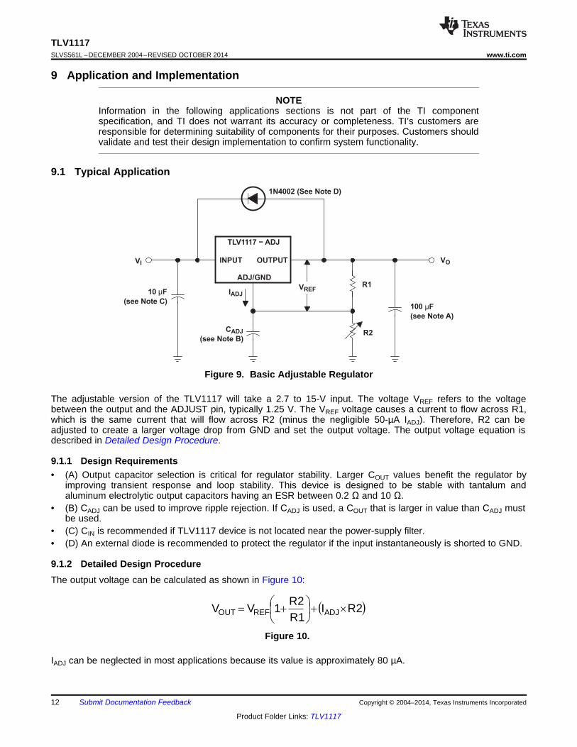
Figure 9. Basic Adjustable Regulator
The adjustable version of the TLV1117 will take a 2.7 to 15-V input. The voltage VREF refers to the voltagebetween the output and the ADJUST pin, typically 1.25 V. The VREF voltage causes a current to flow across R1,which is the same current that will flow across R2 (minus the negligible 50-µA IADJ). Therefore, R2 can beadjusted to create a larger voltage drop from GND and set the output voltage. The output voltage equation isdescribed in Detailed Design Procedure.
9.1.1 Design Requirements• (A) Output capacitor selection is critical for regulator stability. Larger COUT values benefit the regulator by
improving transient response and loop stability. This device is designed to be stable with tantalum andaluminum electrolytic output capacitors having an ESR between 0.2 Ω and 10 Ω.
• (B) CADJ can be used to improve ripple rejection. If CADJ is used, a COUT that is larger in value than CADJ mustbe used.
• (C) CIN is recommended if TLV1117 device is not located near the power-supply filter.• (D) An external diode is recommended to protect the regulator if the input instantaneously is shorted to GND.
9.1.2 Detailed Design ProcedureThe output voltage can be calculated as shown in Figure 10:
Figure 10.
IADJ can be neglected in most applications because its value is approximately 80 µA.
12 Submit Documentation Feedback Copyright © 2004–2014, Texas Instruments Incorporated
Product Folder Links: TLV1117
OUTPUT
INP
UT
OU
TP
UT
AD
J/GN
D
R2
R1Cadj
COUT
PF
Gro
und
Ground
Power
0
0.2
0.4
0.6
0.8
1
1.2
1.4
Load Current (mA)
Dro
po
ut
Vo
ltag
e (V
)
0 800700600500400300200100
TJ = 25C
TJ = 125C
TLV1117www.ti.com SLVS561L –DECEMBER 2004–REVISED OCTOBER 2014
Typical Application (continued)9.1.3 Application Curves
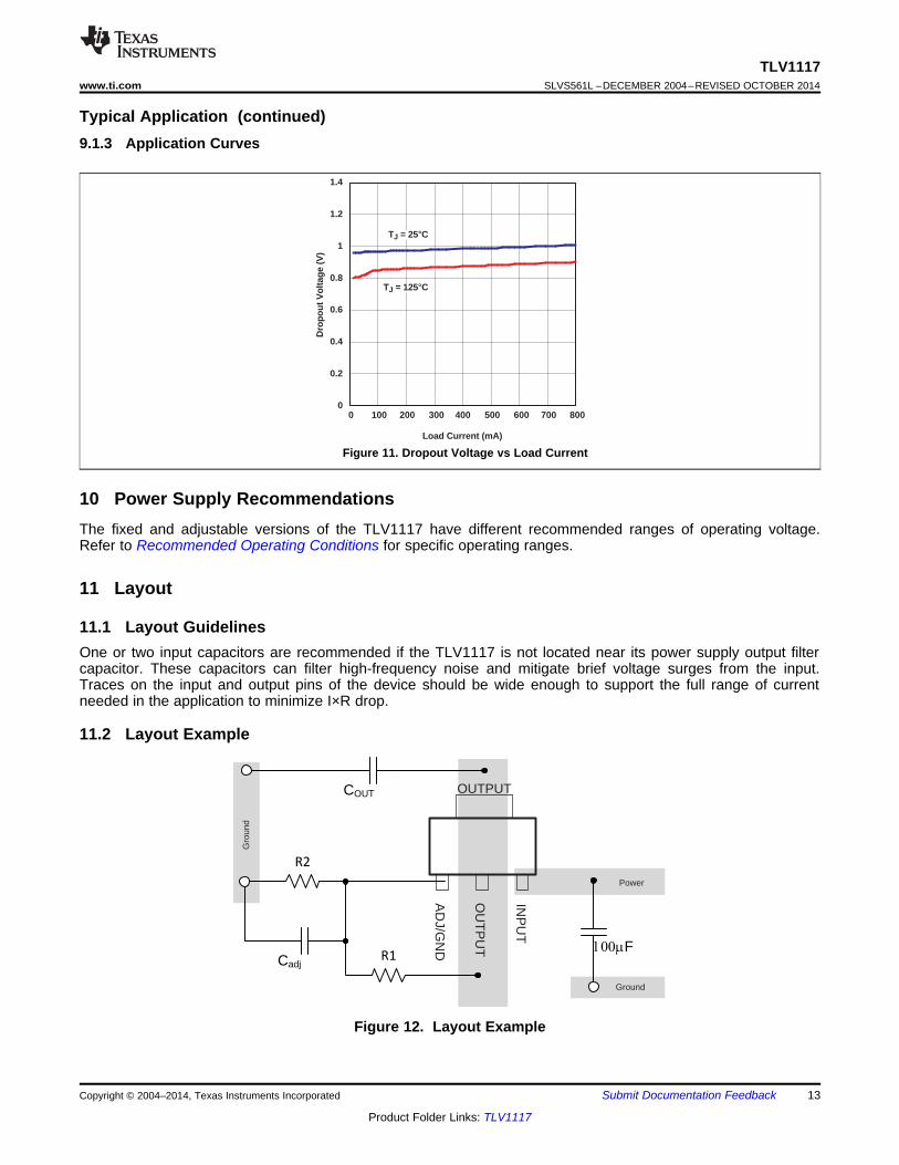
Figure 11. Dropout Voltage vs Load Current
10 Power Supply RecommendationsThe fixed and adjustable versions of the TLV1117 have different recommended ranges of operating voltage.Refer to Recommended Operating Conditions for specific operating ranges.
11 Layout
11.1 Layout GuidelinesOne or two input capacitors are recommended if the TLV1117 is not located near its power supply output filtercapacitor. These capacitors can filter high-frequency noise and mitigate brief voltage surges from the input.Traces on the input and output pins of the device should be wide enough to support the full range of currentneeded in the application to minimize I×R drop.
11.2 Layout Example
Figure 12. Layout Example
Copyright © 2004–2014, Texas Instruments Incorporated Submit Documentation Feedback 13
Product Folder Links: TLV1117

TLV1117SLVS561L –DECEMBER 2004–REVISED OCTOBER 2014 www.ti.com
12 Device and Documentation Support
12.1 TrademarksAll trademarks are the property of their respective owners.
12.2 Electrostatic Discharge CautionThese devices have limited built-in ESD protection. The leads should be shorted together or the device placed in conductive foamduring storage or handling to prevent electrostatic damage to the MOS gates.
12.3 GlossarySLYZ022 — TI Glossary.
This glossary lists and explains terms, acronyms and definitions.
13 Mechanical, Packaging, and Orderable InformationThe following pages include mechanical packaging and orderable information. This information is the mostcurrent data available for the designated devices. This data is subject to change without notice and revision ofthis document. For browser based versions of this data sheet, refer to the left hand navigation.
14 Submit Documentation Feedback Copyright © 2004–2014, Texas Instruments Incorporated
Product Folder Links: TLV1117

PACKAGE OPTION ADDENDUM
www.ti.com 24-Aug-2018
Addendum-Page 1
PACKAGING INFORMATION
Orderable Device Status(1)
Package Type PackageDrawing
Pins PackageQty
Eco Plan(2)
Lead/Ball Finish(6)
MSL Peak Temp(3)
Op Temp (°C) Device Marking(4/5)
Samples
TLV1117-15CDCY ACTIVE SOT-223 DCY 4 80 Green (RoHS& no Sb/Br)
CU SN Level-2-260C-1 YEAR 0 to 125 T2
TLV1117-15CDCYR ACTIVE SOT-223 DCY 4 2500 Green (RoHS& no Sb/Br)
CU SN Level-2-260C-1 YEAR 0 to 125 T2
TLV1117-15CDCYRG3 ACTIVE SOT-223 DCY 4 2500 Green (RoHS& no Sb/Br)
CU SN Level-2-260C-1 YEAR 0 to 125 T2
TLV1117-15CDRJR ACTIVE SON DRJ 8 3000 Green (RoHS& no Sb/Br)
CU NIPDAU Level-2-260C-1 YEAR 0 to 125 ZYH
TLV1117-15IDCY ACTIVE SOT-223 DCY 4 80 Green (RoHS& no Sb/Br)
CU SN Level-2-260C-1 YEAR -40 to 125 T3
TLV1117-15IDCYR ACTIVE SOT-223 DCY 4 2500 Green (RoHS& no Sb/Br)
CU SN Level-2-260C-1 YEAR -40 to 125 T3
TLV1117-15IKVURG3 ACTIVE TO-252 KVU 3 2500 Green (RoHS& no Sb/Br)
CU SN Level-3-260C-168 HR -40 to 125 ZF15
TLV1117-18CDCY ACTIVE SOT-223 DCY 4 80 Green (RoHS& no Sb/Br)
CU SN Level-2-260C-1 YEAR 0 to 125 T4
TLV1117-18CDCYR ACTIVE SOT-223 DCY 4 2500 Green (RoHS& no Sb/Br)
CU SN Level-2-260C-1 YEAR 0 to 125 T4
TLV1117-18CDCYRG3 ACTIVE SOT-223 DCY 4 2500 Green (RoHS& no Sb/Br)
CU SN Level-2-260C-1 YEAR 0 to 125 T4
TLV1117-18CDRJR ACTIVE SON DRJ 8 3000 Green (RoHS& no Sb/Br)
CU NIPDAU Level-2-260C-1 YEAR 0 to 125 ZYK
TLV1117-18CKVURG3 ACTIVE TO-252 KVU 3 2500 Green (RoHS& no Sb/Br)
CU SN Level-3-260C-168 HR 0 to 125 ZE18
TLV1117-18IDCY ACTIVE SOT-223 DCY 4 80 Green (RoHS& no Sb/Br)
CU SN Level-2-260C-1 YEAR -40 to 125 T5
TLV1117-18IDCYR ACTIVE SOT-223 DCY 4 2500 Green (RoHS& no Sb/Br)
CU SN Level-2-260C-1 YEAR -40 to 125 T5
TLV1117-18IDCYRG3 ACTIVE SOT-223 DCY 4 2500 Green (RoHS& no Sb/Br)
CU SN Level-2-260C-1 YEAR -40 to 125 T5
TLV1117-18IDRJR ACTIVE SON DRJ 8 1000 Green (RoHS& no Sb/Br)
CU NIPDAU Level-2-260C-1 YEAR -40 to 125 ZYL
TLV1117-18IKVURG3 ACTIVE TO-252 KVU 3 2500 Green (RoHS& no Sb/Br)
CU SN Level-3-260C-168 HR -40 to 125 ZF18

PACKAGE OPTION ADDENDUM
www.ti.com 24-Aug-2018
Addendum-Page 2
Orderable Device Status(1)
Package Type PackageDrawing
Pins PackageQty
Eco Plan(2)
Lead/Ball Finish(6)
MSL Peak Temp(3)
Op Temp (°C) Device Marking(4/5)
Samples
TLV1117-25CDCY ACTIVE SOT-223 DCY 4 80 Green (RoHS& no Sb/Br)
CU SN Level-2-260C-1 YEAR 0 to 125 T6
TLV1117-25CDCYR ACTIVE SOT-223 DCY 4 2500 Green (RoHS& no Sb/Br)
CU SN Level-2-260C-1 YEAR 0 to 125 T6
TLV1117-25CDCYRG3 ACTIVE SOT-223 DCY 4 2500 Green (RoHS& no Sb/Br)
CU SN Level-2-260C-1 YEAR 0 to 125 T6
TLV1117-25CKVURG3 ACTIVE TO-252 KVU 3 2500 Green (RoHS& no Sb/Br)
CU SN Level-3-260C-168 HR 0 to 125 ZE25
TLV1117-25IDCY ACTIVE SOT-223 DCY 4 80 Green (RoHS& no Sb/Br)
CU SN Level-2-260C-1 YEAR -40 to 125 T8
TLV1117-25IDCYR ACTIVE SOT-223 DCY 4 2500 Green (RoHS& no Sb/Br)
CU SN Level-2-260C-1 YEAR -40 to 125 T8
TLV1117-25IDRJR ACTIVE SON DRJ 8 3000 Green (RoHS& no Sb/Br)
CU NIPDAU Level-2-260C-1 YEAR -40 to 125 ZYN
TLV1117-25IKCS PREVIEW TO-220 KCS 3 50 TBD Call TI Call TI -40 to 125
TLV1117-33CDCY ACTIVE SOT-223 DCY 4 80 Green (RoHS& no Sb/Br)
CU SN Level-2-260C-1 YEAR 0 to 125 V3
TLV1117-33CDCYG3 ACTIVE SOT-223 DCY 4 80 Green (RoHS& no Sb/Br)
CU SN Level-2-260C-1 YEAR 0 to 125 V3
TLV1117-33CDCYR ACTIVE SOT-223 DCY 4 2500 Green (RoHS& no Sb/Br)
CU SN Level-2-260C-1 YEAR 0 to 125 V3
TLV1117-33CDCYRG3 ACTIVE SOT-223 DCY 4 2500 Green (RoHS& no Sb/Br)
CU SN Level-2-260C-1 YEAR 0 to 125 V3
TLV1117-33CDRJR ACTIVE SON DRJ 8 1000 Green (RoHS& no Sb/Br)
CU NIPDAU Level-2-260C-1 YEAR 0 to 125 ZYP
TLV1117-33CKVURG3 ACTIVE TO-252 KVU 3 2500 Green (RoHS& no Sb/Br)
CU SN Level-3-260C-168 HR 0 to 125 ZE33
TLV1117-33DCY PREVIEW SOT-223 DCY 4 80 TBD Call TI Call TI 0 to 125
TLV1117-33IDCY ACTIVE SOT-223 DCY 4 80 Green (RoHS& no Sb/Br)
CU SN Level-2-260C-1 YEAR -40 to 125 (V3, VS)
TLV1117-33IDCYG3 ACTIVE SOT-223 DCY 4 80 Green (RoHS& no Sb/Br)
CU SN Level-2-260C-1 YEAR -40 to 125 (V3, VS)
TLV1117-33IDCYR ACTIVE SOT-223 DCY 4 2500 Green (RoHS& no Sb/Br)
CU SN Level-2-260C-1 YEAR -40 to 125 VS
TLV1117-33IDCYRG3 ACTIVE SOT-223 DCY 4 2500 Green (RoHS& no Sb/Br)
CU SN Level-2-260C-1 YEAR -40 to 125 VS

PACKAGE OPTION ADDENDUM
www.ti.com 24-Aug-2018
Addendum-Page 3
Orderable Device Status(1)
Package Type PackageDrawing
Pins PackageQty
Eco Plan(2)
Lead/Ball Finish(6)
MSL Peak Temp(3)
Op Temp (°C) Device Marking(4/5)
Samples
TLV1117-33IDRJR ACTIVE SON DRJ 8 1000 Green (RoHS& no Sb/Br)
CU NIPDAU Level-2-260C-1 YEAR -40 to 125 ZYR
TLV1117-33IKVURG3 ACTIVE TO-252 KVU 3 2500 Green (RoHS& no Sb/Br)
CU SN Level-3-260C-168 HR -40 to 125 ZF33
TLV1117-50CDCY ACTIVE SOT-223 DCY 4 80 Green (RoHS& no Sb/Br)
CU SN Level-2-260C-1 YEAR 0 to 125 VT
TLV1117-50CDCYG3 ACTIVE SOT-223 DCY 4 80 Green (RoHS& no Sb/Br)
CU SN Level-2-260C-1 YEAR 0 to 125 VT
TLV1117-50CDCYR ACTIVE SOT-223 DCY 4 2500 Green (RoHS& no Sb/Br)
CU SN Level-2-260C-1 YEAR 0 to 125 VT
TLV1117-50CDCYRG3 ACTIVE SOT-223 DCY 4 2500 Green (RoHS& no Sb/Br)
CU SN Level-2-260C-1 YEAR 0 to 125 VT
TLV1117-50CDRJR ACTIVE SON DRJ 8 3000 Green (RoHS& no Sb/Br)
CU NIPDAU Level-2-260C-1 YEAR 0 to 125 ZE50
TLV1117-50CKVURG3 ACTIVE TO-252 KVU 3 2500 Green (RoHS& no Sb/Br)
CU SN Level-3-260C-168 HR 0 to 125 ZE50
TLV1117-50IDCY ACTIVE SOT-223 DCY 4 80 Green (RoHS& no Sb/Br)
CU SN Level-2-260C-1 YEAR -40 to 125 VU
TLV1117-50IDCYR ACTIVE SOT-223 DCY 4 2500 Green (RoHS& no Sb/Br)
CU SN Level-2-260C-1 YEAR -40 to 125 VU
TLV1117-50IDCYRG3 ACTIVE SOT-223 DCY 4 2500 Green (RoHS& no Sb/Br)
CU SN Level-2-260C-1 YEAR -40 to 125 VU
TLV1117-50IDRJR ACTIVE SON DRJ 8 1000 Green (RoHS& no Sb/Br)
CU NIPDAU Level-2-260C-1 YEAR -40 to 125 ZF50
TLV1117-50IDRJRG4 ACTIVE SON DRJ 8 1000 Green (RoHS& no Sb/Br)
CU NIPDAU Level-2-260C-1 YEAR -40 to 125 ZF50
TLV1117-50IKVURG3 ACTIVE TO-252 KVU 3 2500 Green (RoHS& no Sb/Br)
CU SN Level-3-260C-168 HR -40 to 125 ZF50
TLV1117CDCY ACTIVE SOT-223 DCY 4 80 Green (RoHS& no Sb/Br)
CU SN Level-2-260C-1 YEAR 0 to 125 V4
TLV1117CDCYG3 ACTIVE SOT-223 DCY 4 80 Green (RoHS& no Sb/Br)
CU SN Level-2-260C-1 YEAR 0 to 125 V4
TLV1117CDCYR ACTIVE SOT-223 DCY 4 2500 Green (RoHS& no Sb/Br)
CU SN Level-2-260C-1 YEAR 0 to 125 V4
TLV1117CDCYRG3 ACTIVE SOT-223 DCY 4 2500 Green (RoHS& no Sb/Br)
CU SN Level-2-260C-1 YEAR 0 to 125 V4

PACKAGE OPTION ADDENDUM
www.ti.com 24-Aug-2018
Addendum-Page 4
Orderable Device Status(1)
Package Type PackageDrawing
Pins PackageQty
Eco Plan(2)
Lead/Ball Finish(6)
MSL Peak Temp(3)
Op Temp (°C) Device Marking(4/5)
Samples
TLV1117CDRJR ACTIVE SON DRJ 8 1000 Green (RoHS& no Sb/Br)
CU NIPDAU Level-2-260C-1 YEAR 0 to 125 ZYS
TLV1117CKCS ACTIVE TO-220 KCS 3 50 Pb-Free(RoHS)
CU SN N / A for Pkg Type 0 to 125 TLV1117C
TLV1117CKCT ACTIVE TO-220 KCT 3 50 Pb-Free(RoHS)
CU SN N / A for Pkg Type 0 to 125 TLV1117C
TLV1117CKTTR ACTIVE DDPAK/TO-263
KTT 3 500 Green (RoHS& no Sb/Br)
CU SN Level-3-245C-168 HR 0 to 125 TLV1117C
TLV1117CKTTRG3 ACTIVE DDPAK/TO-263
KTT 3 500 Green (RoHS& no Sb/Br)
CU SN Level-3-245C-168 HR 0 to 125 TLV1117C
TLV1117CKVURG3 ACTIVE TO-252 KVU 3 2500 Green (RoHS& no Sb/Br)
CU SN Level-3-260C-168 HR 0 to 125 TV1117
TLV1117IDCY ACTIVE SOT-223 DCY 4 80 Green (RoHS& no Sb/Br)
CU SN Level-2-260C-1 YEAR -40 to 125 V2
TLV1117IDCYG3 ACTIVE SOT-223 DCY 4 80 Green (RoHS& no Sb/Br)
CU SN Level-2-260C-1 YEAR -40 to 125 V2
TLV1117IDCYR ACTIVE SOT-223 DCY 4 2500 Green (RoHS& no Sb/Br)
CU SN Level-2-260C-1 YEAR -40 to 125 V2
TLV1117IDCYRG3 ACTIVE SOT-223 DCY 4 2500 Green (RoHS& no Sb/Br)
CU SN Level-2-260C-1 YEAR -40 to 125 V2
TLV1117IDRJR ACTIVE SON DRJ 8 1000 Green (RoHS& no Sb/Br)
CU NIPDAU Level-2-260C-1 YEAR -40 to 125 ZYT
TLV1117IKCS ACTIVE TO-220 KCS 3 50 Pb-Free(RoHS)
CU SN N / A for Pkg Type -40 to 125 TLV1117I
TLV1117IKCSE3 ACTIVE TO-220 KCS 3 50 Pb-Free(RoHS)
CU SN N / A for Pkg Type -40 to 125 TLV1117I
TLV1117IKTTR ACTIVE DDPAK/TO-263
KTT 3 500 Green (RoHS& no Sb/Br)
CU SN Level-3-245C-168 HR -40 to 125 TLV1117I
TLV1117IKVURG3 ACTIVE TO-252 KVU 3 2500 Green (RoHS& no Sb/Br)
CU SN Level-3-260C-168 HR -40 to 125 TY1117
(1) The marketing status values are defined as follows:ACTIVE: Product device recommended for new designs.LIFEBUY: TI has announced that the device will be discontinued, and a lifetime-buy period is in effect.NRND: Not recommended for new designs. Device is in production to support existing customers, but TI does not recommend using this part in a new design.PREVIEW: Device has been announced but is not in production. Samples may or may not be available.OBSOLETE: TI has discontinued the production of the device.
PACKAGE OPTION ADDENDUM
www.ti.com 24-Aug-2018
Addendum-Page 5
(2) RoHS: TI defines "RoHS" to mean semiconductor products that are compliant with the current EU RoHS requirements for all 10 RoHS substances, including the requirement that RoHS substancedo not exceed 0.1% by weight in homogeneous materials. Where designed to be soldered at high temperatures, "RoHS" products are suitable for use in specified lead-free processes. TI mayreference these types of products as "Pb-Free".RoHS Exempt: TI defines "RoHS Exempt" to mean products that contain lead but are compliant with EU RoHS pursuant to a specific EU RoHS exemption.Green: TI defines "Green" to mean the content of Chlorine (Cl) and Bromine (Br) based flame retardants meet JS709B low halogen requirements of <=1000ppm threshold. Antimony trioxide basedflame retardants must also meet the <=1000ppm threshold requirement.
(3) MSL, Peak Temp. - The Moisture Sensitivity Level rating according to the JEDEC industry standard classifications, and peak solder temperature.
(4) There may be additional marking, which relates to the logo, the lot trace code information, or the environmental category on the device.
(5) Multiple Device Markings will be inside parentheses. Only one Device Marking contained in parentheses and separated by a "~" will appear on a device. If a line is indented then it is a continuationof the previous line and the two combined represent the entire Device Marking for that device.
(6) Lead/Ball Finish - Orderable Devices may have multiple material finish options. Finish options are separated by a vertical ruled line. Lead/Ball Finish values may wrap to two lines if the finishvalue exceeds the maximum column width.
Important Information and Disclaimer:The information provided on this page represents TI's knowledge and belief as of the date that it is provided. TI bases its knowledge and belief on informationprovided by third parties, and makes no representation or warranty as to the accuracy of such information. Efforts are underway to better integrate information from third parties. TI has taken andcontinues to take reasonable steps to provide representative and accurate information but may not have conducted destructive testing or chemical analysis on incoming materials and chemicals.TI and TI suppliers consider certain information to be proprietary, and thus CAS numbers and other limited information may not be available for release.
In no event shall TI's liability arising out of such information exceed the total purchase price of the TI part(s) at issue in this document sold by TI to Customer on an annual basis.

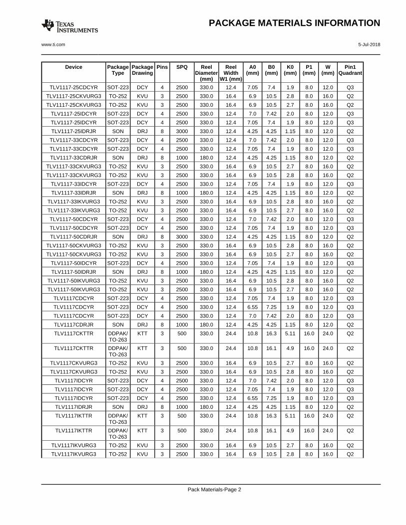
TAPE AND REEL INFORMATION
*All dimensions are nominal
Device PackageType
PackageDrawing
Pins SPQ ReelDiameter
(mm)
ReelWidth
W1 (mm)
A0(mm)
B0(mm)
K0(mm)
P1(mm)
W(mm)
Pin1Quadrant
TLV1117-15CDCYR SOT-223 DCY 4 2500 330.0 12.4 7.05 7.4 1.9 8.0 12.0 Q3
TLV1117-15CDCYR SOT-223 DCY 4 2500 330.0 12.4 7.0 7.42 2.0 8.0 12.0 Q3
TLV1117-15CDRJR SON DRJ 8 3000 330.0 12.4 4.25 4.25 1.15 8.0 12.0 Q2
TLV1117-15IDCYR SOT-223 DCY 4 2500 330.0 12.4 7.05 7.4 1.9 8.0 12.0 Q3
TLV1117-15IDCYR SOT-223 DCY 4 2500 330.0 12.4 7.0 7.42 2.0 8.0 12.0 Q3
TLV1117-15IKVURG3 TO-252 KVU 3 2500 330.0 16.4 6.9 10.5 2.7 8.0 16.0 Q2
TLV1117-15IKVURG3 TO-252 KVU 3 2500 330.0 16.4 6.9 10.5 2.8 8.0 16.0 Q2
TLV1117-18CDCYR SOT-223 DCY 4 2500 330.0 12.4 6.55 7.25 1.9 8.0 12.0 Q3
TLV1117-18CDCYR SOT-223 DCY 4 2500 330.0 12.4 7.0 7.42 2.0 8.0 12.0 Q3
TLV1117-18CDRJR SON DRJ 8 3000 330.0 12.4 4.25 4.25 1.15 8.0 12.0 Q2
TLV1117-18CKVURG3 TO-252 KVU 3 2500 330.0 16.4 6.9 10.5 2.8 8.0 16.0 Q2
TLV1117-18CKVURG3 TO-252 KVU 3 2500 330.0 16.4 6.9 10.5 2.7 8.0 16.0 Q2
TLV1117-18IDCYR SOT-223 DCY 4 2500 330.0 12.4 7.0 7.42 2.0 8.0 12.0 Q3
TLV1117-18IDCYR SOT-223 DCY 4 2500 330.0 12.4 6.55 7.25 1.9 8.0 12.0 Q3
TLV1117-18IDRJR SON DRJ 8 1000 180.0 12.4 4.25 4.25 1.15 8.0 12.0 Q2
TLV1117-18IKVURG3 TO-252 KVU 3 2500 330.0 16.4 6.9 10.5 2.8 8.0 16.0 Q2
TLV1117-18IKVURG3 TO-252 KVU 3 2500 330.0 16.4 6.9 10.5 2.7 8.0 16.0 Q2
TLV1117-25CDCYR SOT-223 DCY 4 2500 330.0 12.4 7.0 7.42 2.0 8.0 12.0 Q3
PACKAGE MATERIALS INFORMATION
www.ti.com 5-Jul-2018
Pack Materials-Page 1
Device PackageType
PackageDrawing
Pins SPQ ReelDiameter
(mm)
ReelWidth
W1 (mm)
A0(mm)
B0(mm)
K0(mm)
P1(mm)
W(mm)
Pin1Quadrant
TLV1117-25CDCYR SOT-223 DCY 4 2500 330.0 12.4 7.05 7.4 1.9 8.0 12.0 Q3
TLV1117-25CKVURG3 TO-252 KVU 3 2500 330.0 16.4 6.9 10.5 2.8 8.0 16.0 Q2
TLV1117-25CKVURG3 TO-252 KVU 3 2500 330.0 16.4 6.9 10.5 2.7 8.0 16.0 Q2
TLV1117-25IDCYR SOT-223 DCY 4 2500 330.0 12.4 7.0 7.42 2.0 8.0 12.0 Q3
TLV1117-25IDCYR SOT-223 DCY 4 2500 330.0 12.4 7.05 7.4 1.9 8.0 12.0 Q3
TLV1117-25IDRJR SON DRJ 8 3000 330.0 12.4 4.25 4.25 1.15 8.0 12.0 Q2
TLV1117-33CDCYR SOT-223 DCY 4 2500 330.0 12.4 7.0 7.42 2.0 8.0 12.0 Q3
TLV1117-33CDCYR SOT-223 DCY 4 2500 330.0 12.4 7.05 7.4 1.9 8.0 12.0 Q3
TLV1117-33CDRJR SON DRJ 8 1000 180.0 12.4 4.25 4.25 1.15 8.0 12.0 Q2
TLV1117-33CKVURG3 TO-252 KVU 3 2500 330.0 16.4 6.9 10.5 2.7 8.0 16.0 Q2
TLV1117-33CKVURG3 TO-252 KVU 3 2500 330.0 16.4 6.9 10.5 2.8 8.0 16.0 Q2
TLV1117-33IDCYR SOT-223 DCY 4 2500 330.0 12.4 7.05 7.4 1.9 8.0 12.0 Q3
TLV1117-33IDRJR SON DRJ 8 1000 180.0 12.4 4.25 4.25 1.15 8.0 12.0 Q2
TLV1117-33IKVURG3 TO-252 KVU 3 2500 330.0 16.4 6.9 10.5 2.8 8.0 16.0 Q2
TLV1117-33IKVURG3 TO-252 KVU 3 2500 330.0 16.4 6.9 10.5 2.7 8.0 16.0 Q2
TLV1117-50CDCYR SOT-223 DCY 4 2500 330.0 12.4 7.0 7.42 2.0 8.0 12.0 Q3
TLV1117-50CDCYR SOT-223 DCY 4 2500 330.0 12.4 7.05 7.4 1.9 8.0 12.0 Q3
TLV1117-50CDRJR SON DRJ 8 3000 330.0 12.4 4.25 4.25 1.15 8.0 12.0 Q2
TLV1117-50CKVURG3 TO-252 KVU 3 2500 330.0 16.4 6.9 10.5 2.8 8.0 16.0 Q2
TLV1117-50CKVURG3 TO-252 KVU 3 2500 330.0 16.4 6.9 10.5 2.7 8.0 16.0 Q2
TLV1117-50IDCYR SOT-223 DCY 4 2500 330.0 12.4 7.05 7.4 1.9 8.0 12.0 Q3
TLV1117-50IDRJR SON DRJ 8 1000 180.0 12.4 4.25 4.25 1.15 8.0 12.0 Q2
TLV1117-50IKVURG3 TO-252 KVU 3 2500 330.0 16.4 6.9 10.5 2.8 8.0 16.0 Q2
TLV1117-50IKVURG3 TO-252 KVU 3 2500 330.0 16.4 6.9 10.5 2.7 8.0 16.0 Q2
TLV1117CDCYR SOT-223 DCY 4 2500 330.0 12.4 7.05 7.4 1.9 8.0 12.0 Q3
TLV1117CDCYR SOT-223 DCY 4 2500 330.0 12.4 6.55 7.25 1.9 8.0 12.0 Q3
TLV1117CDCYR SOT-223 DCY 4 2500 330.0 12.4 7.0 7.42 2.0 8.0 12.0 Q3
TLV1117CDRJR SON DRJ 8 1000 180.0 12.4 4.25 4.25 1.15 8.0 12.0 Q2
TLV1117CKTTR DDPAK/TO-263
KTT 3 500 330.0 24.4 10.8 16.3 5.11 16.0 24.0 Q2
TLV1117CKTTR DDPAK/TO-263
KTT 3 500 330.0 24.4 10.8 16.1 4.9 16.0 24.0 Q2
TLV1117CKVURG3 TO-252 KVU 3 2500 330.0 16.4 6.9 10.5 2.7 8.0 16.0 Q2
TLV1117CKVURG3 TO-252 KVU 3 2500 330.0 16.4 6.9 10.5 2.8 8.0 16.0 Q2
TLV1117IDCYR SOT-223 DCY 4 2500 330.0 12.4 7.0 7.42 2.0 8.0 12.0 Q3
TLV1117IDCYR SOT-223 DCY 4 2500 330.0 12.4 7.05 7.4 1.9 8.0 12.0 Q3
TLV1117IDCYR SOT-223 DCY 4 2500 330.0 12.4 6.55 7.25 1.9 8.0 12.0 Q3
TLV1117IDRJR SON DRJ 8 1000 180.0 12.4 4.25 4.25 1.15 8.0 12.0 Q2
TLV1117IKTTR DDPAK/TO-263
KTT 3 500 330.0 24.4 10.8 16.3 5.11 16.0 24.0 Q2
TLV1117IKTTR DDPAK/TO-263
KTT 3 500 330.0 24.4 10.8 16.1 4.9 16.0 24.0 Q2
TLV1117IKVURG3 TO-252 KVU 3 2500 330.0 16.4 6.9 10.5 2.7 8.0 16.0 Q2
TLV1117IKVURG3 TO-252 KVU 3 2500 330.0 16.4 6.9 10.5 2.8 8.0 16.0 Q2
PACKAGE MATERIALS INFORMATION
www.ti.com 5-Jul-2018
Pack Materials-Page 2

*All dimensions are nominal
Device Package Type Package Drawing Pins SPQ Length (mm) Width (mm) Height (mm)
TLV1117-15CDCYR SOT-223 DCY 4 2500 340.0 340.0 38.0
TLV1117-15CDCYR SOT-223 DCY 4 2500 350.0 334.0 47.0
TLV1117-15CDRJR SON DRJ 8 3000 367.0 367.0 35.0
TLV1117-15IDCYR SOT-223 DCY 4 2500 340.0 340.0 38.0
TLV1117-15IDCYR SOT-223 DCY 4 2500 350.0 334.0 47.0
TLV1117-15IKVURG3 TO-252 KVU 3 2500 340.0 340.0 38.0
TLV1117-15IKVURG3 TO-252 KVU 3 2500 350.0 334.0 47.0
TLV1117-18CDCYR SOT-223 DCY 4 2500 336.0 336.0 48.0
TLV1117-18CDCYR SOT-223 DCY 4 2500 350.0 334.0 47.0
TLV1117-18CDRJR SON DRJ 8 3000 367.0 367.0 35.0
TLV1117-18CKVURG3 TO-252 KVU 3 2500 350.0 334.0 47.0
TLV1117-18CKVURG3 TO-252 KVU 3 2500 340.0 340.0 38.0
TLV1117-18IDCYR SOT-223 DCY 4 2500 350.0 334.0 47.0
TLV1117-18IDCYR SOT-223 DCY 4 2500 336.0 336.0 48.0
TLV1117-18IDRJR SON DRJ 8 1000 210.0 185.0 35.0
TLV1117-18IKVURG3 TO-252 KVU 3 2500 350.0 334.0 47.0
TLV1117-18IKVURG3 TO-252 KVU 3 2500 340.0 340.0 38.0
TLV1117-25CDCYR SOT-223 DCY 4 2500 350.0 334.0 47.0
TLV1117-25CDCYR SOT-223 DCY 4 2500 340.0 340.0 38.0
PACKAGE MATERIALS INFORMATION
www.ti.com 5-Jul-2018
Pack Materials-Page 3

Device Package Type Package Drawing Pins SPQ Length (mm) Width (mm) Height (mm)
TLV1117-25CKVURG3 TO-252 KVU 3 2500 350.0 334.0 47.0
TLV1117-25CKVURG3 TO-252 KVU 3 2500 340.0 340.0 38.0
TLV1117-25IDCYR SOT-223 DCY 4 2500 350.0 334.0 47.0
TLV1117-25IDCYR SOT-223 DCY 4 2500 340.0 340.0 38.0
TLV1117-25IDRJR SON DRJ 8 3000 367.0 367.0 35.0
TLV1117-33CDCYR SOT-223 DCY 4 2500 350.0 334.0 47.0
TLV1117-33CDCYR SOT-223 DCY 4 2500 340.0 340.0 38.0
TLV1117-33CDRJR SON DRJ 8 1000 210.0 185.0 35.0
TLV1117-33CKVURG3 TO-252 KVU 3 2500 340.0 340.0 38.0
TLV1117-33CKVURG3 TO-252 KVU 3 2500 350.0 334.0 47.0
TLV1117-33IDCYR SOT-223 DCY 4 2500 340.0 340.0 38.0
TLV1117-33IDRJR SON DRJ 8 1000 210.0 185.0 35.0
TLV1117-33IKVURG3 TO-252 KVU 3 2500 350.0 334.0 47.0
TLV1117-33IKVURG3 TO-252 KVU 3 2500 340.0 340.0 38.0
TLV1117-50CDCYR SOT-223 DCY 4 2500 350.0 334.0 47.0
TLV1117-50CDCYR SOT-223 DCY 4 2500 340.0 340.0 38.0
TLV1117-50CDRJR SON DRJ 8 3000 367.0 367.0 35.0
TLV1117-50CKVURG3 TO-252 KVU 3 2500 350.0 334.0 47.0
TLV1117-50CKVURG3 TO-252 KVU 3 2500 340.0 340.0 38.0
TLV1117-50IDCYR SOT-223 DCY 4 2500 340.0 340.0 38.0
TLV1117-50IDRJR SON DRJ 8 1000 210.0 185.0 35.0
TLV1117-50IKVURG3 TO-252 KVU 3 2500 350.0 334.0 47.0
TLV1117-50IKVURG3 TO-252 KVU 3 2500 340.0 340.0 38.0
TLV1117CDCYR SOT-223 DCY 4 2500 340.0 340.0 38.0
TLV1117CDCYR SOT-223 DCY 4 2500 336.0 336.0 48.0
TLV1117CDCYR SOT-223 DCY 4 2500 350.0 334.0 47.0
TLV1117CDRJR SON DRJ 8 1000 210.0 185.0 35.0
TLV1117CKTTR DDPAK/TO-263 KTT 3 500 340.0 340.0 38.0
TLV1117CKTTR DDPAK/TO-263 KTT 3 500 350.0 334.0 47.0
TLV1117CKVURG3 TO-252 KVU 3 2500 340.0 340.0 38.0
TLV1117CKVURG3 TO-252 KVU 3 2500 350.0 334.0 47.0
TLV1117IDCYR SOT-223 DCY 4 2500 350.0 334.0 47.0
TLV1117IDCYR SOT-223 DCY 4 2500 340.0 340.0 38.0
TLV1117IDCYR SOT-223 DCY 4 2500 336.0 336.0 48.0
TLV1117IDRJR SON DRJ 8 1000 210.0 185.0 35.0
TLV1117IKTTR DDPAK/TO-263 KTT 3 500 340.0 340.0 38.0
TLV1117IKTTR DDPAK/TO-263 KTT 3 500 350.0 334.0 47.0
TLV1117IKVURG3 TO-252 KVU 3 2500 340.0 340.0 38.0
TLV1117IKVURG3 TO-252 KVU 3 2500 350.0 334.0 47.0
PACKAGE MATERIALS INFORMATION
www.ti.com 5-Jul-2018
Pack Materials-Page 4
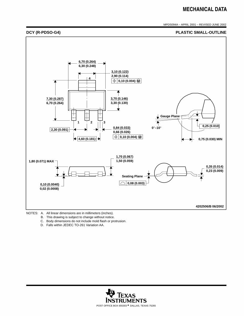
MECHANICAL DATA
MPDS094A – APRIL 2001 – REVISED JUNE 2002
POST OFFICE BOX 655303 • DALLAS, TEXAS 75265
DCY (R-PDSO-G4) PLASTIC SMALL-OUTLINE
4202506/B 06/2002
6,30 (0.248)6,70 (0.264)
2,90 (0.114)3,10 (0.122)
6,70 (0.264)7,30 (0.287) 3,70 (0.146)
3,30 (0.130)
0,02 (0.0008)0,10 (0.0040)
1,50 (0.059)1,70 (0.067)
0,23 (0.009)0,35 (0.014)
1 2 3
4
0,66 (0.026)0,84 (0.033)
1,80 (0.071) MAX
Seating Plane
0°–10°
Gauge Plane
0,75 (0.030) MIN
0,25 (0.010)
0,08 (0.003)
0,10 (0.004) M
2,30 (0.091)
4,60 (0.181) M0,10 (0.004)
NOTES: A. All linear dimensions are in millimeters (inches).B. This drawing is subject to change without notice.C. Body dimensions do not include mold flash or protrusion.D. Falls within JEDEC TO-261 Variation AA.


www.ti.com
PACKAGE OUTLINE
C
5.4604.953
10.419.40
2.29
4.58
3X 0.8900.635 1.02
0.61
1.270.89
2.52 MAX
0.610.46
4.32MIN
5.21 MIN
-800.130.001.78
1.40
0.610.46
A
6.706.35
B 6.225.97
0.51GAGE PLANE
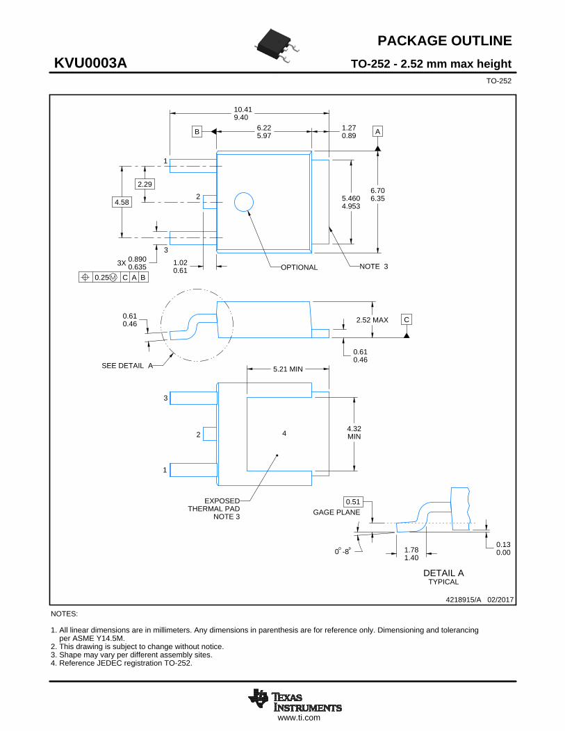
TO-252 - 2.52 mm max heightKVU0003ATO-252
4218915/A 02/2017
NOTES: 1. All linear dimensions are in millimeters. Any dimensions in parenthesis are for reference only. Dimensioning and tolerancing per ASME Y14.5M. 2. This drawing is subject to change without notice.3. Shape may vary per different assembly sites.4. Reference JEDEC registration TO-252.
1
2
3
0.25 C A BOPTIONAL NOTE 3
SCALE 1.500
SEE DETAIL A
EXPOSEDTHERMAL PAD
NOTE 3
1
2
3
4
A 7.000
DETAIL ATYPICAL

www.ti.com
EXAMPLE BOARD LAYOUT
0.07 MAXALL AROUND 0.07 MIN
ALL AROUND
(6.15)
(5.55)(4.58)
2X (1)2X (2.75)
(4.2) (2.5)(R0.05) TYP
TO-252 - 2.52 mm max heightKVU0003ATO-252
4218915/A 02/2017
LAND PATTERN EXAMPLEEXPOSED METAL SHOWN
SCALE:6X
PKG
SYMM
3
1
4
NOTES: (continued) 5. This package is designed to be soldered to a thermal pad on the board. For more information, see Texas Instruments literature numbers SLMA002(www.ti.com/lit/slm002) and SLMA004 (www.ti.com/lit/slma004).6. Vias are optional depending on application, refer to device data sheet. It is recommended that vias under paste be filled, plugged or tented.
SOLDER MASKOPENING
METAL
EXPOSEDMETAL
SOLDER MASK DETAILSNOT TO SCALE
NON SOLDER MASKDEFINED
METAL UNDERSOLDER MASK
SOLDER MASKOPENING
EXPOSEDMETAL
SOLDER MASKDEFINED
www.ti.com
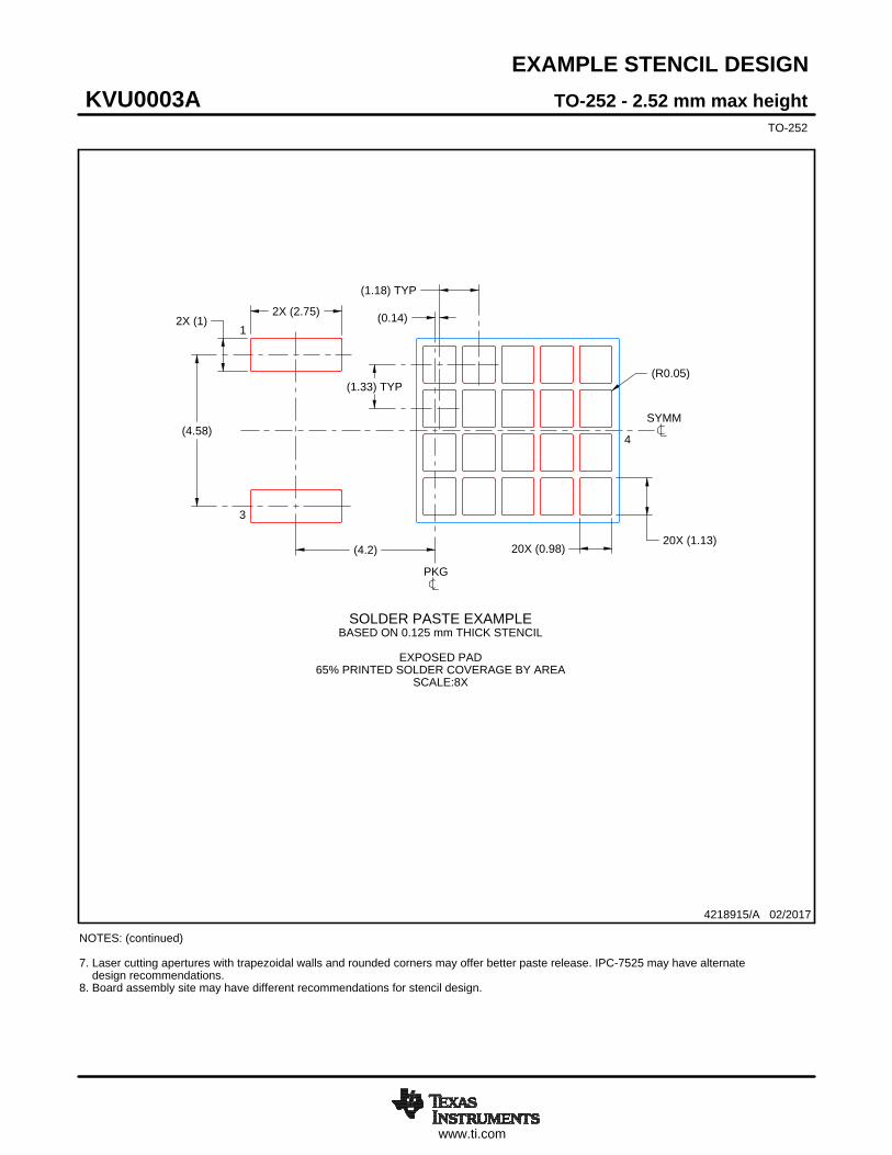
EXAMPLE STENCIL DESIGN
20X (0.98)20X (1.13)
(R0.05)
2X (2.75)2X (1)
(4.58)
(1.33) TYP
(1.18) TYP
(0.14)
(4.2)
TO-252 - 2.52 mm max heightKVU0003ATO-252
4218915/A 02/2017
PKG
NOTES: (continued) 7. Laser cutting apertures with trapezoidal walls and rounded corners may offer better paste release. IPC-7525 may have alternate design recommendations.8. Board assembly site may have different recommendations for stencil design.
SOLDER PASTE EXAMPLEBASED ON 0.125 mm THICK STENCIL
EXPOSED PAD
65% PRINTED SOLDER COVERAGE BY AREASCALE:8X
SYMM
3
1
4


www.ti.com
PACKAGE OUTLINE
9.259.05
6.56.1
2.92.6
10.369.96
13.1212.70
3X3.9 MAX
3X 1.361.23
3X 0.900.77
( 3.84)
5.08
2X 2.54
8.558.15
12.512.1
(6.3)
19.65 MAX
4.74.4
1.321.22
2.792.59
0.470.34
4222214/B 08/2018
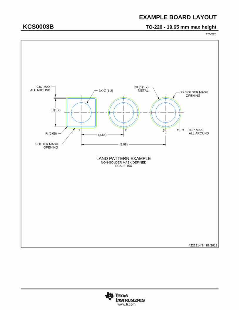
TO-220 - 19.65 mm max heightKCS0003BTO-220
NOTES: 1. Dimensions are in millimeters. Any dimension in brackets or parenthesis are for reference only. Dimensioning and tolerancing per ASME Y14.5M.2. This drawing is subject to change without notice.3. Reference JEDEC registration TO-220.
1 3
SCALE 0.850
www.ti.com
EXAMPLE BOARD LAYOUT
0.07 MAXALL AROUND
0.07 MAXALL AROUND
(1.7)
3X (1.2)
(2.54)
(5.08)
R (0.05)
2X (1.7)METAL 2X SOLDER MASK
OPENING
4222214/B 08/2018
TO-220 - 19.65 mm max heightKCS0003BTO-220
LAND PATTERN EXAMPLENON-SOLDER MASK DEFINED
SCALE:15X
1 2 3
OPENINGSOLDER MASK

ASIZESCALE
4PAGE
4 OF4222214REV
B
REVISIONSENGINEER / DRAFTSMANDATEECRDESCRIPTIONREVJ. NOQUIL / T. LEQUANG10/22/20152151829RELEASE NEW DRAWINGA
E. PREISS / K. SINCERBOX08/17/20182175971CORRECT NOTE 1A

IMPORTANT NOTICE
Texas Instruments Incorporated (TI) reserves the right to make corrections, enhancements, improvements and other changes to itssemiconductor products and services per JESD46, latest issue, and to discontinue any product or service per JESD48, latest issue. Buyersshould obtain the latest relevant information before placing orders and should verify that such information is current and complete.TI’s published terms of sale for semiconductor products (http://www.ti.com/sc/docs/stdterms.htm) apply to the sale of packaged integratedcircuit products that TI has qualified and released to market. Additional terms may apply to the use or sale of other types of TI products andservices.Reproduction of significant portions of TI information in TI data sheets is permissible only if reproduction is without alteration and isaccompanied by all associated warranties, conditions, limitations, and notices. TI is not responsible or liable for such reproduceddocumentation. Information of third parties may be subject to additional restrictions. Resale of TI products or services with statementsdifferent from or beyond the parameters stated by TI for that product or service voids all express and any implied warranties for theassociated TI product or service and is an unfair and deceptive business practice. TI is not responsible or liable for any such statements.Buyers and others who are developing systems that incorporate TI products (collectively, “Designers”) understand and agree that Designersremain responsible for using their independent analysis, evaluation and judgment in designing their applications and that Designers havefull and exclusive responsibility to assure the safety of Designers' applications and compliance of their applications (and of all TI productsused in or for Designers’ applications) with all applicable regulations, laws and other applicable requirements. Designer represents that, withrespect to their applications, Designer has all the necessary expertise to create and implement safeguards that (1) anticipate dangerousconsequences of failures, (2) monitor failures and their consequences, and (3) lessen the likelihood of failures that might cause harm andtake appropriate actions. Designer agrees that prior to using or distributing any applications that include TI products, Designer willthoroughly test such applications and the functionality of such TI products as used in such applications.TI’s provision of technical, application or other design advice, quality characterization, reliability data or other services or information,including, but not limited to, reference designs and materials relating to evaluation modules, (collectively, “TI Resources”) are intended toassist designers who are developing applications that incorporate TI products; by downloading, accessing or using TI Resources in anyway, Designer (individually or, if Designer is acting on behalf of a company, Designer’s company) agrees to use any particular TI Resourcesolely for this purpose and subject to the terms of this Notice.TI’s provision of TI Resources does not expand or otherwise alter TI’s applicable published warranties or warranty disclaimers for TIproducts, and no additional obligations or liabilities arise from TI providing such TI Resources. TI reserves the right to make corrections,enhancements, improvements and other changes to its TI Resources. TI has not conducted any testing other than that specificallydescribed in the published documentation for a particular TI Resource.Designer is authorized to use, copy and modify any individual TI Resource only in connection with the development of applications thatinclude the TI product(s) identified in such TI Resource. NO OTHER LICENSE, EXPRESS OR IMPLIED, BY ESTOPPEL OR OTHERWISETO ANY OTHER TI INTELLECTUAL PROPERTY RIGHT, AND NO LICENSE TO ANY TECHNOLOGY OR INTELLECTUAL PROPERTYRIGHT OF TI OR ANY THIRD PARTY IS GRANTED HEREIN, including but not limited to any patent right, copyright, mask work right, orother intellectual property right relating to any combination, machine, or process in which TI products or services are used. Informationregarding or referencing third-party products or services does not constitute a license to use such products or services, or a warranty orendorsement thereof. Use of TI Resources may require a license from a third party under the patents or other intellectual property of thethird party, or a license from TI under the patents or other intellectual property of TI.TI RESOURCES ARE PROVIDED “AS IS” AND WITH ALL FAULTS. TI DISCLAIMS ALL OTHER WARRANTIES ORREPRESENTATIONS, EXPRESS OR IMPLIED, REGARDING RESOURCES OR USE THEREOF, INCLUDING BUT NOT LIMITED TOACCURACY OR COMPLETENESS, TITLE, ANY EPIDEMIC FAILURE WARRANTY AND ANY IMPLIED WARRANTIES OFMERCHANTABILITY, FITNESS FOR A PARTICULAR PURPOSE, AND NON-INFRINGEMENT OF ANY THIRD PARTY INTELLECTUALPROPERTY RIGHTS. TI SHALL NOT BE LIABLE FOR AND SHALL NOT DEFEND OR INDEMNIFY DESIGNER AGAINST ANY CLAIM,INCLUDING BUT NOT LIMITED TO ANY INFRINGEMENT CLAIM THAT RELATES TO OR IS BASED ON ANY COMBINATION OFPRODUCTS EVEN IF DESCRIBED IN TI RESOURCES OR OTHERWISE. IN NO EVENT SHALL TI BE LIABLE FOR ANY ACTUAL,DIRECT, SPECIAL, COLLATERAL, INDIRECT, PUNITIVE, INCIDENTAL, CONSEQUENTIAL OR EXEMPLARY DAMAGES INCONNECTION WITH OR ARISING OUT OF TI RESOURCES OR USE THEREOF, AND REGARDLESS OF WHETHER TI HAS BEENADVISED OF THE POSSIBILITY OF SUCH DAMAGES.Unless TI has explicitly designated an individual product as meeting the requirements of a particular industry standard (e.g., ISO/TS 16949and ISO 26262), TI is not responsible for any failure to meet such industry standard requirements.Where TI specifically promotes products as facilitating functional safety or as compliant with industry functional safety standards, suchproducts are intended to help enable customers to design and create their own applications that meet applicable functional safety standardsand requirements. Using products in an application does not by itself establish any safety features in the application. Designers mustensure compliance with safety-related requirements and standards applicable to their applications. Designer may not use any TI products inlife-critical medical equipment unless authorized officers of the parties have executed a special contract specifically governing such use.Life-critical medical equipment is medical equipment where failure of such equipment would cause serious bodily injury or death (e.g., lifesupport, pacemakers, defibrillators, heart pumps, neurostimulators, and implantables). Such equipment includes, without limitation, allmedical devices identified by the U.S. Food and Drug Administration as Class III devices and equivalent classifications outside the U.S.TI may expressly designate certain products as completing a particular qualification (e.g., Q100, Military Grade, or Enhanced Product).Designers agree that it has the necessary expertise to select the product with the appropriate qualification designation for their applicationsand that proper product selection is at Designers’ own risk. Designers are solely responsible for compliance with all legal and regulatoryrequirements in connection with such selection.Designer will fully indemnify TI and its representatives against any damages, costs, losses, and/or liabilities arising out of Designer’s non-compliance with the terms and provisions of this Notice.
Mailing Address: Texas Instruments, Post Office Box 655303, Dallas, Texas 75265Copyright © 2018, Texas Instruments Incorporated
![15 Watt Interchangeable Plug Series PSA15R Wall Plug ... · [Type text] PSA15R Characteristics Input: AC Input Voltage Rating 100 to 240V AC FCC Part 15 Class B AC Input Voltage Range](https://img.pdfslide.net/doc/110x75/5ae023107f8b9a1c248cd1f8/15-watt-interchangeable-plug-series-psa15r-wall-plug-type-text-psa15r-characteristics.jpg)