Embed Size (px)
Citation preview
1
TMDXEVM6678L EVM
Technical Reference Manual
Version 1.0
Literature Number: SPRUH58
Revised April 2011
Document Copyright
Publication Title:
TMDXEVM6678L Technical Reference Manual All
Rights Reserved. Reproduction, adaptation, or
translation without prior written permission is
prohibited, except as allowed under copyright laws.
2
EVALUATION BOARD / KIT / MODULE (EVM) WARNINGS, RESTRICTIONS AND DISCLAIMER
Not for Diagnostic Use: For Feasibility Evaluation Only in Laboratory/Development
Environments
The EVM may not be used for diagnostic purposes.
This EVM is intended solely for evaluation and development purposes. It is not intended for
use and may not be used as all, or part of an end equipment product.
This EVM should be used solely by qualified engineers and technicians who are familiar with
the risks associated with handling electrical and mechanical components, systems and
subsystems.
Your Obligations and Responsibilities
Please consult the EVM documentation, including but not limited to any user guides, setup
guides or getting started guides, and other warnings prior to using the EVM. Any use of the
EVM outside of the specified operating range may cause danger to users and/or produce
unintended results, inaccurate operation, and permanent damage to the EVM and
associated electronics. You acknowledge and agree that:
You are responsible for compliance with all applicable Federal, State and local regulatory
requirements (including but not limited to Food and Drug Administration regulations, UL,
CSA, VDE, CE, RoHS and WEEE,) that relate to your use (and that of your employees,
contractors or designees) of the EVM for evaluation, testing and other purposes.
You are responsible for the safety of you and your employees and contractors when
using or handling the EVM. Further, you are responsible for ensuring that any contacts
or interfaces between the EVM and any human body are designed to be safe and to
avoid the risk of electrical shock.
You will defend, indemnify and hold TI, its licensors and their representatives harmless
from and against any and all claims, damages, losses, expenses, costs and liabilities
(collectively, “Claims”) arising out of, or in connection with any use of the EVM that is
not in accordance with the terms of this agreement. This obligation shall apply whether
Claims arise under the law of tort or contract or any other legal theory, and even if the
EVM fails to perform as described or expected.
Warning
The EVM board may get very hot during use. Specifically, the DSP, its heat
sink and power supply circuits all heat up during operation. This will not harm
the EVM. Use care when touching the unit when operating or allow it to cool
after use before handling. If unit is operated in an environment that limits
free air flow, a fan may be needed.
3
Preface
About this Document
This document is a Technical Reference Manual for the TMS320C6678 Evaluation Module
(TMDXEVM6678L) designed and developed by Advantech Limited for Texas Instruments, Inc.
Notational Conventions
This document uses the following conventions:
Program listings, program examples, and interactive displays are shown in a mono spaced
font. Examples use bold for emphasis, and interactive displays use bold to distinguish
commands that you enter from items that the system displays (such as prompts, command
output, error messages, etc.).
Square brackets ( [ and ] ) identify an optional parameter. If you use an optional parameter,
you specify the information within the brackets. Unless the square brackets are in a bold
typeface, do not enter the brackets themselves.
Underlined, italicized non-bold text in a command is used to mark place holder text that
should be replaced by the appropriate value for the user’s configuration.
4
Trademarks
The Texas Instruments logo and Texas Instruments are registered trademarks of Texas
Instruments. Trademarks of Texas Instruments include: TI, XDS, Code Composer, Code
Composer Studio, Probe Point, Code Explorer, DSP / BIOS, RTDX, Online DSP Lab, TMS320,
TMS320C54x, TMS320C55x, TMS320C62x, TMS320C64x, TMS320C67x, TMS320C5000, and
TMS320C6000.
MS-DOS, Windows, Windows XP, and Windows NT are trademarks of Microsoft
Corporation.
UNIX is a registered trademark of The Open Group in the United States and other countries.
All other brand, product names, and service names are trademarks or registered trademarks
of their respective companies or organizations.
5
Document Revision History
Release Chapter Description of Change
1.0 All First Release
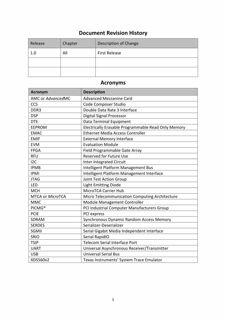
Acronyms
Acronym Description
AMC or AdvancedMC Advanced Mezzanine Card
CCS Code Composer Studio
DDR3 Double Data Rate 3 Interface
DSP Digital Signal Processor
DTE Data Terminal Equipment
EEPROM Electrically Erasable Programmable Read Only Memory
EMAC Ethernet Media Access Controller
EMIF External Memory Interface
EVM Evaluation Module
FPGA Field Programmable Gate Array
RFU Reserved for Future Use
I2C Inter Integrated Circuit
IPMB Intelligent Platform Management Bus
IPMI Intelligent Platform Management Interface
JTAG Joint Test Action Group
LED Light Emitting Diode
MCH MicroTCA Carrier Hub
MTCA or MicroTCA Micro Telecommunication Computing Architecture
MMC Module Management Controller
PICMG® PCI Industrial Computer Manufacturers Group
PCIE PCI express
SDRAM Synchronous Dynamic Random Access Memory
SERDES Serializer-Deserializer
SGMII Serial Gigabit Media Independent Interface
SRIO Serial RapidIO
TSIP Telecom Serial Interface Port
UART Universal Asynchronous Receiver/Transmitter
USB Universal Serial Bus
XDS560v2 Texas Instruments’ System Trace Emulator
6
Table of Contents
1. Overview..............................................................................................................................11
1.1 Key Features...............................................................................................................11
1.2 Functional Overview ..................................................................................................12
1.3 Basic Operation..........................................................................................................12
1.4 Boot Mode and Boot Configuration Switch Setting...................................................13
1.5 Power Supply .............................................................................................................14
2. Introduction to the TMDXEVM6678L board.......................................................................15
2.1 Memory Map .............................................................................................................15
2.2 EVM Boot Mode and Boot Configuration Switch Settings ........................................18
2.3 JTAG - Emulation Overview........................................................................................18
2.4 Clock Domains............................................................................................................19
2.5 I2C Boot EEPROM / SPI NOR Flash.............................................................................19
2.6 FPGA...........................................................................................................................20
2.7 Gigabit Ethernet Connections....................................................................................21
2.8 Serial RapidIO (SRIO) Interface ..................................................................................22
2.9 DDR3 External Memory Interface..............................................................................22
2.10 16-bit Asynchronous External Memory Interface (EMIF-16)...................................23
2.11 HyperLink Interface..................................................................................................24
2.12 PCIe Interface...........................................................................................................24
2.13 Telecom Serial Interface Port (TSIP) ........................................................................25
2.14 UART Interface.........................................................................................................25
2.15 Module Management Controller (MMC) for IPMI ..................................................26
2.16 Expansion Header ....................................................................................................27
3. TMDXEVM6678L Board Physical Specifications .................................................................28
3.1 Board Layout ..............................................................................................................28
3.2 Connector Index.........................................................................................................29
3.2.1 560V2_PWR1, XDS560v2 Mezzanine Power Connector..............................29
3.2.2 AMC1, AMC Edge Connector .......................................................................30
3.2.3 COM1, UART3 Pin Connector.......................................................................32
3.2.4 COM_SEL1, UART Route Select Connector ..................................................32
3.2.5 DC_IN1, DC Power Input Jack Connector.....................................................33
3.2.6 EMU1, TI 60-Pin DSP JTAG Connector..........................................................33
3.2.7 FAN1, FAN Connector...................................................................................34
3.2.8 HyperLink1, HyperLink Connector ...............................................................35
3.2.9 LAN1, Ethernet Connector...........................................................................36
3.2.10 PMBUS1, PMBUS Connector for Smart-Reflex Control .............................36
3.2.11 TAP_FPGA1, FPGA JTAG Connector (For Factory Use Only).......................37
3.2.12 TAP_MMC1, MSP430 JTAG Connector (For Factory Use Only)..................37
3.2.13 TEST_PH1, Expansion Header (EMIF-16, SPI, GPIO, Timer I/O, I2C, and
UART) .......................................................................................................................38
3.2.14 USB1, Mini-USB Connector........................................................................39
3.3 DIP and Pushbutton Switches ....................................................................................40
3.3.1 RST_FULL1, Full Reset ..................................................................................40
3.3.2 RST_COLD1, Cold Reset................................................................................40
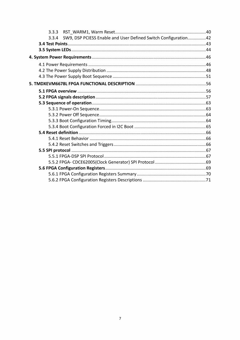
7
3.3.3 RST_WARM1, Warm Reset...........................................................................40
3.3.4 SW9, DSP PCIESS Enable and User Defined Switch Configuration...............42
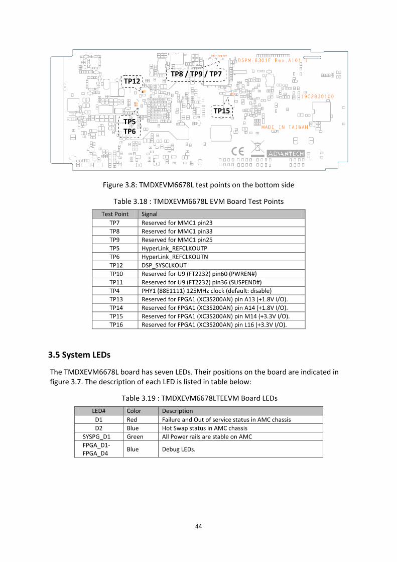
3.4 Test Points..................................................................................................................43
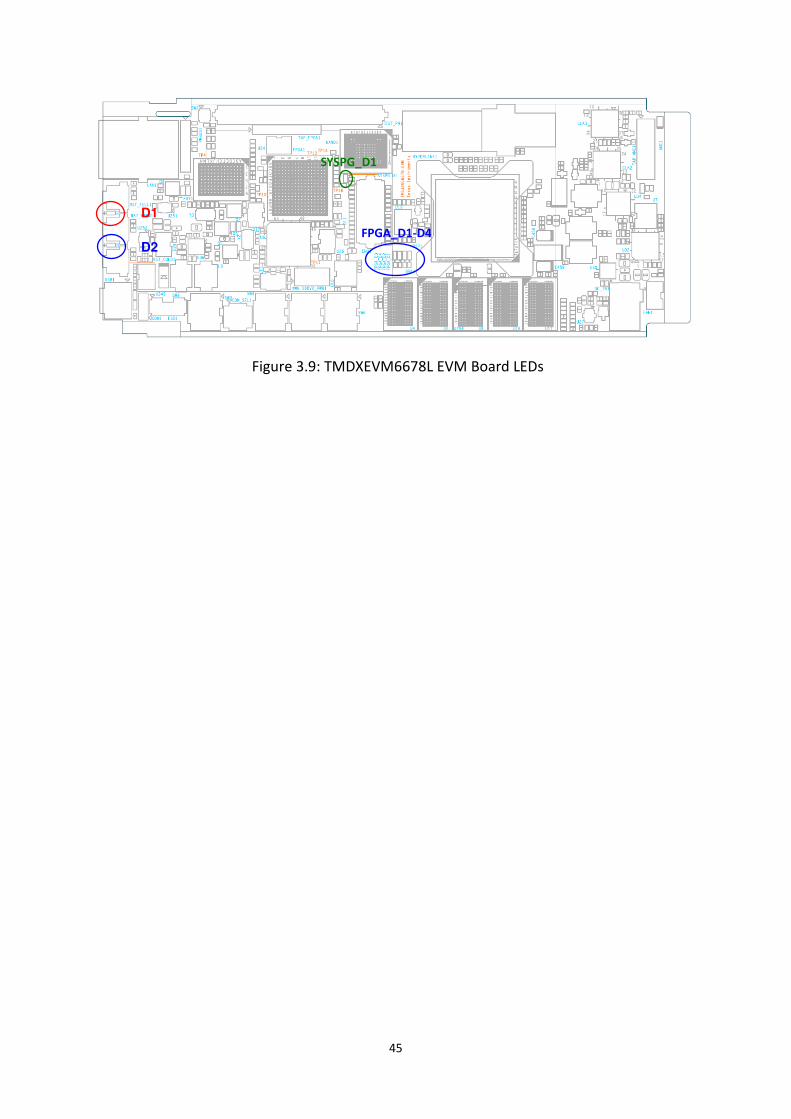
3.5 System LEDs ...............................................................................................................44
4. System Power Requirements ..............................................................................................46
4.1 Power Requirements .................................................................................................46
4.2 The Power Supply Distribution ..................................................................................48
4.3 The Power Supply Boot Sequence .............................................................................51
5. TMDXEVM6678L FPGA FUNCTIONAL DESCRIPTION ..........................................................56
5.1 FPGA overview ..........................................................................................................56
5.2 FPGA signals description ...........................................................................................57
5.3 Sequence of operation ..............................................................................................63
5.3.1 Power-On Sequence........................................................................................63
5.3.2 Power Off Sequence........................................................................................64
5.3.3 Boot Configuration Timing..............................................................................64
5.3.4 Boot Configuration Forced in I2C Boot ...........................................................65
5.4 Reset definition .........................................................................................................66
5.4.1 Reset Behavior ................................................................................................66
5.4.2 Reset Switches and Triggers ............................................................................66
5.5 SPI protocol ...............................................................................................................67
5.5.1 FPGA-DSP SPI Protocol ....................................................................................67
5.5.2 FPGA- CDCE62005(Clock Generator) SPI Protocol ..........................................69
5.6 FPGA Configuration Registers...................................................................................69
5.6.1 FPGA Configuration Registers Summary.........................................................70
5.6.2 FPGA Configuration Registers Descriptions ....................................................71
8
List of Figures
Figure 1.1: Block Diagram of TMDXEVM6678L EVM ...............................................................12
Figure 1.2: TMDXEVM6678L EVM Layout................................................................................13
Figure 2.1: TMDXEVM6678L EVM JTAG emulation .................................................................19
Figure 2.2: TMDXEVM6678L EVM Clock Domains...................................................................19
Figure 2.3: TMDXEVM6678L EVM FPGA Connections.............................................................21
Figure 2.4: TMDXEVM6678L EVM Ethernet Routing...............................................................21
Figure 2.5: TMDXEVM6678L EVM SRIO Port Connections ......................................................22
Figure 2.6: TMDXEVM6678L EVM SDRAM ..............................................................................23
Figure 2.7: TMDXEVM6678L EVM EMIF-16 connections.........................................................23
Figure 2.8: TMDXEVM6678L EVM HyperLink connections......................................................24
Figure 2.9: TMDXEVM6678L EVM PCIE Port Connections.......................................................24
Figure 2.10: TMDXEVM6678L EVM TSIP connections .............................................................25
Figure 2.11: TMDXEVM6678L EVM UART Connections...........................................................26
Figure 2.12: TMDXEVM6678L EVM MMC Connections for IPMI.............................................27
Figure 3.1: TMDXEVM6678L EVM Board Assembly Layout – TOP view..................................28
Figure 3.2: TMDXEVM6678L EVM Board layout – Bottom view .............................................29
Figure 3.3 : The HyperLink Connector .....................................................................................35
Figure 3.4 : TAP_FPGA1 function diagram ...............................................................................37
Figure 3.5 : SW3, SW4, SW5, and SW6 default settings ..........................................................41
Figure 3.6 : SW9 default settings .............................................................................................43
Figure 3.7: TMDXEVM6678L test points on top side ...............................................................43
Figure 3.8: TMDXEVM6678L test points on the bottom side ..................................................44
Figure 3.9: TMDXEVM6678L EVM Board LEDs ........................................................................45
Figure 4.1: All the AMC power supply on TMDXEVM6678L EVM ...........................................49
Figure 4.2: The CVDD and VCC1V0 (CVDD1) power design on TMDXEVM6678L EVM ...........50
Figure 4.3: The VCC3_AUX power design on TMDXEVM6678L EVM ......................................50
Figure 4.4: The VCC1V5 power design on TMDXEVM6678L EVM...........................................51
Figure 4.5: The VCC5 power design on TMDXEVM6678L EVM ...............................................51
Figure 4.6: Initial Power Up Sequence Timing Diagram ..........................................................54
Figure 4.7: Initial Power Down Sequence Timing Diagram .....................................................55
Figure 5-1 Power-On Reset Boot Configuration Timing ..........................................................65
9
Figure 5-2 Reset-Full Switch/Trigger Boot Configuration Timing .........................................65
Figure 5-3; The SPI access form the TMS320C6678 to the FPGA (WRITE / high level) ...........67
Figure 5-4: The SPI access form the TMS320C6678 to the FPGA (WRITE) ..............................68
Figure 5-5: The SPI access form the TMS320C6678 to the FPGA (READ / high level) .............68
Figure 5-6: The SPI access form the TMS320C6678 to the FPGA (READ) ................................68
Figure 5-7: The SPI access form the FPGA to the CDCE62005 (WRITE) ...................................69
Figure 5-8: The SPI access form the FPGA to the CDCE62005 (READ).....................................69
10
List of Tables
Table 2.1: TMS320C6678 Memory Map ..................................................................................16
Table 3.1 : TMDXEVM6678L EVM Board Connectors..............................................................29
Table 3.2 : XDS560v2 Power Connector pin out ......................................................................30
Table 3.3: AMC Edge Connector...............................................................................................30
Table 3.4 : UART Connector pin out.........................................................................................32
Table 3.5 : UART Path Select Connector pin out ......................................................................33
Table 3.6: DSP JTAG Connector pin out....................................................................................34
Table 3.7 : FAN1 Connector pin out .........................................................................................35
Table 3.8 : The HyperLink Connector .......................................................................................35
Table 3.9 : Ethernet Connector pin out....................................................................................36
Table 3.10 : PMBUS1 pin out ...................................................................................................36
Table 3.11 : FPGA JTAG Connector pin out ..............................................................................37
Table 3.12 : MSP430 JTAG Connector pin out..........................................................................38
Table 3.13 : Test Header pin out...............................................................................................38
Table 3.14 : Mini-USB Connector pin out.................................................................................40
Table 3.15 : TMDXEVM6678L EVM Board Switches.................................................................40
Table 3.16 : SW3-SW6, DSP Configuration Switch ...................................................................42
Table 3.17: SW9, DSP PCI Express Enable and User Switch .....................................................43
Table 3.18 : TMDXEVM6678L EVM Board Test Points.............................................................44
Table 3.19 : TMDXEVM6678LTEEVM Board LEDs.....................................................................44
Table 4.1: EVM Voltage Table ..................................................................................................47
Table 4.2: Each Current Requirements on each device of EVM board ...................................48
Table 4.3: The power-up and down timing on the TMDXEVM6678L......................................53
Table 5.1 : TMDXEVM6678L EVM FPGA Pin Description.........................................................57
Table 5.2 : TMS320C6678 EVM FPGA Memory Map...............................................................70
Table 5.3 : FPGA Configuration Registers Summary ................................................................70
11
1. Overview
This chapter provides an overview of the TMDXEVM6678L along with the key features and
block diagram.
1.1 Key Features
1.2 Functional Overview
1.3 Basic Operation
1.4 Configuration Switch Settings
1.5 Power Supply
1.1 Key Features
The TMDXEVM6678L is a high performance, cost-efficient, standalone development
platform that enables users to evaluate and develop applications for the Texas Instruments’
TMS320C6678 Digital Signal Processor (DSP). The Evaluation Module (EVM) also serves as a
hardware reference design platform for the TMS320C6678 DSP. The EVM’s form-factor is
equivalent to a single-wide PICMG® AMC.0 R2.0 AdvancedMC module.
Schematics, code examples and application notes are available to ease the hardware
development process and to reduce the time to market.
The key features of the TMDXEVM6678L EVM are:
� Texas Instruments' multi-core DSP – TMS320C6678
� 512 Mbytes of DDR3-1333 Memory
� 64 Mbytes of NAND Flash
� 16MB SPI NOR FLASH
� Two Gigabit Ethernet ports supporting 10/100/1000 Mbps data-rate – one on
AMC connector and one RJ-45 connector
� 170 pin B+ style AMC Interface containing SRIO, PCIe, Gigabit Ethernet and TDM
� High Performance connector for HyperLink
� 128K-byte I2C EEPROM for booting
� 2 User LEDs, 5 Banks of DIP Switches and 4 Software-controlled LEDs
� RS232 Serial interface on 3-Pin header or UART over mini-USB connector
� EMIF, Timer, SPI, UART on 80-pin expansion header
12
� On-Board XDS100 type Emulation using High-speed USB 2.0 interface
� TI 60-Pin JTAG header to support all external emulator types
� Module Management Controller (MMC) for Intelligent Platform Management
Interface (IPMI)
� Optional XDS560v2 System Trace Emulation Mezzanine Card
� Powered by DC power-brick adaptor (12V/3.0A) or AMC Carrier backplane
� PICMG® AMC.0 R2.0 single width, full height AdvancedMC module
1.2 Functional Overview
The TMS320C66x™ DSPs (including the TMS320C6678 device) are the highest-performance
fixed / floating-point DSP generation in the TMS320C6000™ DSP platform. The
TMS320C6678 device is based on the third-generation high-performance, advanced
VelociTI™ very-long-instruction-word (VLIW) architecture developed by Texas Instruments
(TI), designed specifically for high density wireline / wireless media gateway infrastructure.
It is an ideal solution for IP border gateways, video transcoding and translation, video-server
and intelligent voice and video recognition applications. The C66x devices are backward
code-compatible from previous devices that are part of the C6000™ DSP platform.
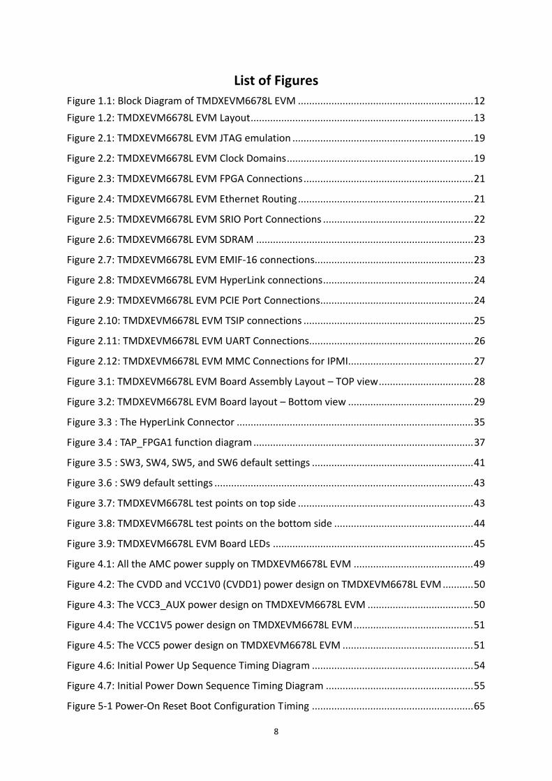
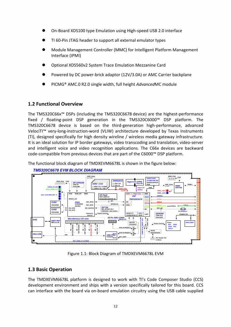
The functional block diagram of TMDXEVM6678L is shown in the figure below:
FPGA_DONE LED
User controlled LED - 4
SYSPG_D1 LED
MMC_LED1
TSIPx2Level-Shifter
TMS320C6678 EVM BLOCK DIAGRAM
DIP_SWITCH
DEBUG_LED TMS320C6678N25Q128A21BSF40F
UARTMAC1
MDIOJTAG&EMU[0:1]
EMU[2:17]
MAC0
EMIF
PCIEx2
I2C
DDR3 Hyper Link
GP
IO[0
:15
](1.8
V)
Miscellaneous I/O conn.
EM
IF16
(1.8
V)
DS
P_
UA
RT
(3.3
V)
DS
P_
SP
I(1.8
V)
DS
P_
I2C
(1.8
V)
RS232
MAX3221EAE
DS
P_
UA
RT
FT2232HLUSB-JTAG
CH-B
CH-A
DSP_SGMII_P1 & MDIO
DSP_UART
ENET PHY
Mini-USB USB
RJ45
88E1111-B2
TSIPx2
SRIOx4
NAND FLASH
NAND512R3A2D
ZA6E
SGMIIx1
(512Mb 64M X8)
SRIOx4
PCIEx2
SPI
GPIO
MMC
MMC JTAGJTAG
EMIF
IPMB-LAMC_State
#0
PWR CONN
POWER 12V
DSP
from MMC
AMC_State
AT25128B
SPI
GPIO[0:15]
DIP SW
SPI EEPROM
RAM
Others
FPGA
PowerPower Control
(MSP430)
PHY
DDR3 -1333
DDR3-1333
1. 64M X 16 / 512MB
2. 128M X 16 / 1GB
w/ ECC
(XILINX)
JTAG MMC
DSP_SPI#1FPGAXC3S200AN
DSP_GPIO
HyperLink
ROM_SPI
CLK_SPI3
CLK_SPI2
50Gbps
DSP
iPass+HD
DSP_I2C
to FPGA
TSIPx2
Power Control
128k-bit
Control
Sequence
FPGA JTAG JTAG
NOR 128M-bitSPI Flash
60-Pin EMU CONN.
HyperLink CONN.
JTAG & EMU[0:1]
EMU[2:17]
MU
XM
UXJTAG & EMU[0:1]
Pin-Header 3x1
2.54mm
CDCE62005
CLK#1
CLK#2
CDCE62005
DS
P_
SG
MII_
P1
& M
DIO
24AA1025
EEPROM128k-byte
BM_GPIO(0~15) /
PCIESSEN / User define
NU Resistors
MMC_LED2
SWITCH
(TS3L301)
1. 1Gb X 16
2. 1Gb X 8
DDR3(ECC)
Figure 1.1: Block Diagram of TMDXEVM6678L EVM
1.3 Basic Operation
The TMDXEVM6678L platform is designed to work with TI’s Code Composer Studio (CCS)
development environment and ships with a version specifically tailored for this board. CCS
can interface with the board via on-board emulation circuitry using the USB cable supplied
13
along with this EVM or through an external emulator.
The EVM comes with the Texas Instruments Multicore Software Development Kit (MCSDK)
for SYS/BIOS OS. The BIOS MCSDK provides the core foundational building blocks that
facilitate application software development on TI's high performance and multicore DSPs.
The MCSDK also includes an out-of-box demonstration; see the "MCSDK Getting Started
Guide".
To start operating the board, follow instructions in the Quick Start Guide. This guide
provides instruction for proper connections and configuration for running the POST and
OOB Demos. After completing the POST and OOB Demos, proceed with installing CCS and
the EVM support files by following the instructions on the DVD. This process will install all
the necessary development tools, drivers and documentation.
After the installation has completed, follow the steps below to run Code Composer Studio.
1. Power-on the board using the power brick adaptor (12V/3.0A) supplied along with this
EVM or inserting this EVM board into a MicroTCA chassis or AMC carrier backplane.
2. Connect USB cable from host PC to EVM board.
3. Launch Code Composer Studio from host PC by double clicking on its icon on the PC
desktop.
Detailed information about the EVM including examples and reference materials are
available in the DVD included with this EVM kit.
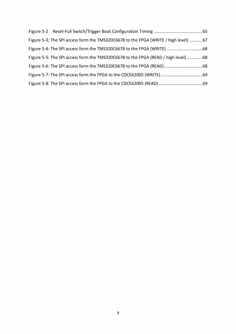
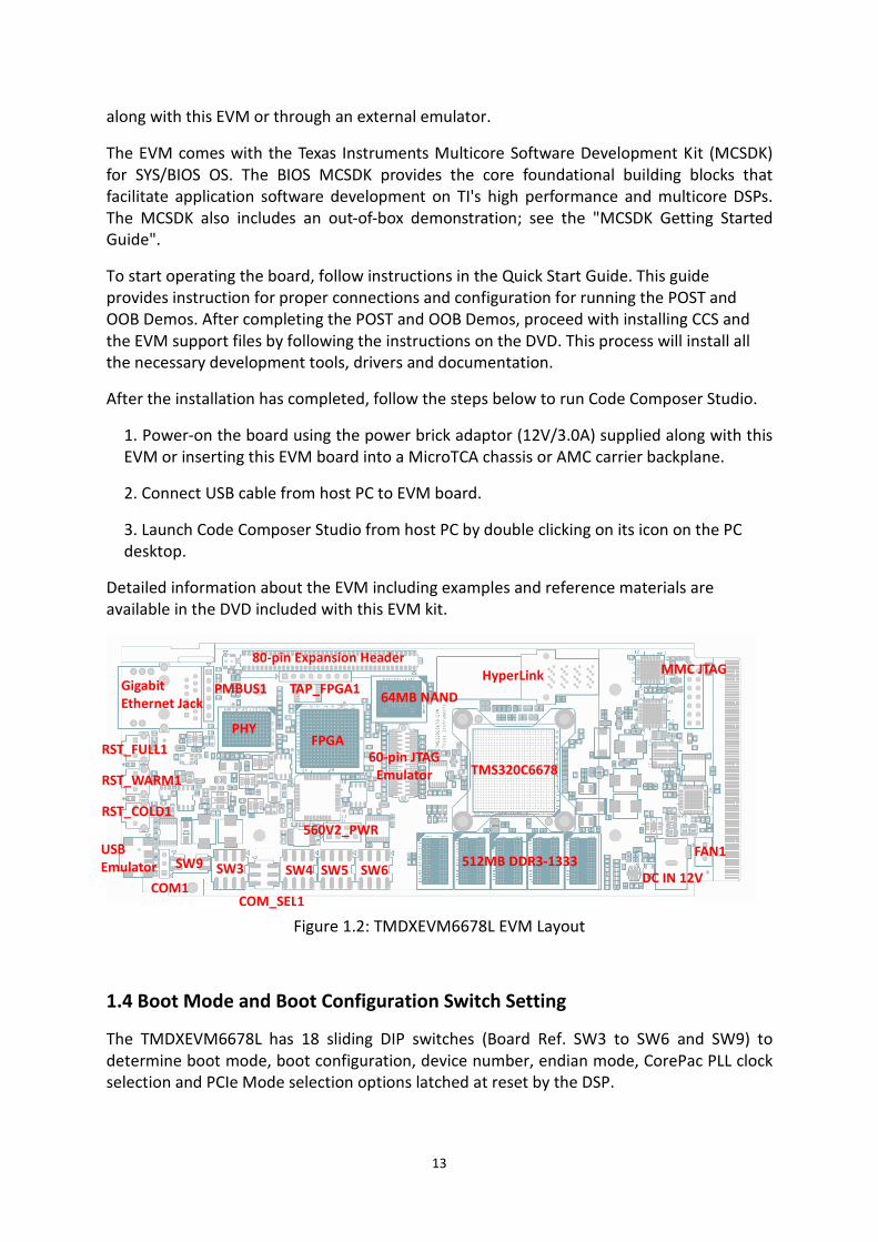
Figure 1.2: TMDXEVM6678L EVM Layout
1.4 Boot Mode and Boot Configuration Switch Setting
The TMDXEVM6678L has 18 sliding DIP switches (Board Ref. SW3 to SW6 and SW9) to
determine boot mode, boot configuration, device number, endian mode, CorePac PLL clock
selection and PCIe Mode selection options latched at reset by the DSP.
PHY FPGA
60-pin JTAG
Emulator
64MB NAND
MMC JTAG HyperLink
TMS320C6678
DC IN 12V
FAN1 512MB DDR3-1333
80-pin Expansion Header
TAP_FPGA1 PMBUS1 Gigabit
Ethernet Jack
SW6 SW5 SW4 SW3 SW9
COM1
USB
Emulator
COM_SEL1
560V2_PWR
1
RST_FULL1
RST_WARM1
RST_COLD1
14
1.5 Power Supply
The TMDXEVM6678L can be powered from a single +12V / 3.0A DC (36W) external power
supply connected to the DC power jack (DC_IN1). Internally, +12V input is converted into
required voltage levels using local DC-DC converters.
• CVDD (+0.90V~+1.05V) used for the DSP Core logic
• +1.0V is used for DSP internal memory and HyperLink/SRIO/SGMII/PCIe SERDES
termination of DSP
• +1.5V is used for DDR3 buffers of DSP, HyperLink/SRIO/SGMII/PCIe SERDES regulators
in DSP and DDR3 DRAM chips
• +1.8V is used for DSP PLLs, DSP LVCMOS I/Os and FPGA I/Os driving the DSP
• +2.5V is used for Gigabit Ethernet PHY core
• +1.2V is used for FPGA core and Gigabit Ethernet PHY core
• +3.3V is used for FPGA I/Os
• +5V and +3.3V is used to power optional XDS560v2 mezzanine card
• The DC power jack connector is a 2.5mm barrel-type plug with center-tip as positive
polarity
The TMDXEVM6678L can also draw power from the AMC edge connector (AMC1). If the
board is inserted into a PICMG® MicroTCA.0 R1.0 compliant system chassis or AMC Carrier
backplane, an external +12V supply from DC jack (DC_IN1) is not required.
15
2. Introduction to the TMDXEVM6678L board
This chapter provides an introduction and details of interfaces for the TMDXEVM6678L
board. It contains:
2.1 Memory Map
2.2 EVM Boot mode and Boot configuration switch settings
2.3 JTAG - Emulation Overview
2.4 Clock Domains
2.5 I2C boot EEPROM / SPI NOR Flash
2.6 FPGA
2.7 Gigabit Ethernet PHY
2.8 Serial RapidIO (SRIO) Interfaces
2.9 DDR3 External Memory Interfaces
2.10 16-bit Asynchronous External Memory Interface
2.11 HyperLink Interface
2.12 PCIe Interface
2.13 Telecom Serial Interface Port (TSIP)
2.14 UART Interfaces
2.15 Module Management Controller for IPMI
2.16 Additional Headers
2.1 Memory Map
The memory map of the TMS320C6678 device is as shown in Table 1. The external memory
configuration register address ranges in the TMS320C6678 device begin at the hex address
location 0x7000 0000 for EMIFA and hex address location 0x8000 0000 for DDR3 Memory
Controller.
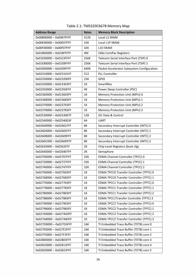
16
Table 2.1: TMS320C6678 Memory Map
Address Range Bytes Memory Block Description
0x00800000 – 0x0087FFFF 512K Local L2 SRAM
0x00E00000 – 0x00E07FFF 32K Local L1P SRAM
0x00F00000 – 0x00F07FFF 32K L1D SRAM
0x01800000 – 0x01BFFFFF 4M C66x CorePac Registers
0x01E00000 – 0x01E3FFFF 256K Telecom Serial Interface Port (TSIP) 0
0x01E80000 – 0x01EBFFFF 256K Telecom Serial Interface Port (TSIP) 1
0x02000000 – 0x0209FFFF 640K Packet Accelerator Subsystem Configuration
0x02310000 – 0x023101FF 512 PLL Controller
0x02320000 – 0x023200FF 256 GPIO
0x02330000 – 0x023303FF 1K SmartRlex
0x02350000 – 0x02350FFF 4K Power Sleep Controller (PSC)
0x02360000 – 0x023603FF 1K Memory Protection Unit (MPU) 0
0x02368000 – 0x023683FF 1K Memory Protection Unit (MPU) 1
0x02370000 – 0x023703FF 1K Memory Protection Unit (MPU) 2
0x02378000 – 0x023783FF 1K Memory Protection Unit (MPU) 3
0x02530000 – 0x0253007F 128 I2C Data & Control
0x02540000 – 0x0254003F 64 UART
0x02600000 – 0x02601FFF 8K Secondary Interrupt Controller (INTC) 0
0x02604000 – 0x02605FFF 8K Secondary Interrupt Controller (INTC) 1
0x02608000 – 0x02609FFF 8K Secondary Interrupt Controller (INTC) 2
0x0260C000 – 0x0260DFFF 8K Secondary Interrupt Controller (INTC) 3
0x02620000 – 0x026207F 2K Chip-Level Registers (boot cfg)
0x02640000 – 0x026407FF 2K Semaphore
0x02700000 – 0x02707FFF 32K EDMA Channel Controller (TPCC) 0
0x02720000 – 0x02727FFF 32K EDMA Channel Controller (TPCC) 1
0x02740000 – 0x02747FFF 32K EDMA Channel Controller (TPCC) 2
0x02760000 – 0x027603FF 1K EDMA TPCC0 Transfer Controller (TPTC) 0
0x02768000 – 0x027683FF 1K EDMA TPCC0 Transfer Controller (TPTC) 1
0x02770000 – 0x027703FF 1K EDMA TPCC1 Transfer Controller (TPTC) 0
0x02778000 – 0x027783FF 1K EDMA TPCC1 Transfer Controller (TPTC) 1
0x02780000 – 0x027803FF 1K EDMA TPCC1 Transfer Controller (TPTC) 2
0x02788000 – 0x027883FF 1K EDMA TPCC1Transfer Controller (TPTC) 3
0x02790000 – 0x027903FF 1K EDMA TPCC2 Transfer Controller (TPTC) 0
0x02798000 – 0x027983FF 1K EDMA TPCC2 Transfer Controller (TPTC) 1
0x027A0000 – 0x027A03FF 1K EDMA TPCC2 Transfer Controller (TPTC) 2
0x027A8000 – 0x027A83FF 1K EDMA TPCC2 Transfer Controller (TPTC) 3
0x027D0000 – 0x027D3FFF 16K TI Embedded Trace Buffer (TETB) core 0
0x027E0000 – 0x027E3FFF 16K TI Embedded Trace Buffer (TETB) core 1
0x027F0000 – 0x027F3FFF 16K TI Embedded Trace Buffer (TETB) core 2
0x02800000 – 0x02803FFF 16K TI Embedded Trace Buffer (TETB) core 3
0x02810000 – 0x02813FFF 16K TI Embedded Trace Buffer (TETB) core 4
0x02820000 – 0x02823FFF 16K TI Embedded Trace Buffer (TETB) core 5
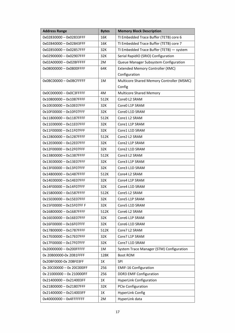
17
Address Range Bytes Memory Block Description
0x02830000 – 0x02833FFF 16K TI Embedded Trace Buffer (TETB) core 6
0x02840000 – 0x02843FFF 16K TI Embedded Trace Buffer (TETB) core 7
0x02850000 – 0x02857FFF 32K TI Embedded Trace Buffer (TETB) — system
0x02900000 – 0x02907FFF 32K Serial RapidIO (SRIO) Configuration
0x02A00000 – 0x02BFFFFF 2M Queue Manager Subsystem Configuration
0x08000000 – 0x0800FFFF 64K Extended Memory Controller (XMC)
Configuration
0x0BC00000 – 0x0BCFFFFF 1M Multicore Shared Memory Controller (MSMC)
Config
0x0C000000 – 0x0C3FFFFF 4M Multicore Shared Memory
0x10800000 – 0x1087FFFF 512K Core0 L2 SRAM
0x10E00000 – 0x10E07FFF 32K Core0 L1P SRAM
0x10F00000 – 0x10F07FFF 32K Core0 L1D SRAM
0x11800000 – 0x1187FFFF 512K Core1 L2 SRAM
0x11E00000 – 0x11E07FFF 32K Core1 L1P SRAM
0x11F00000 – 0x11F07FFF 32K Core1 L1D SRAM
0x12800000 – 0x1287FFFF 512K Core2 L2 SRAM
0x12E00000 – 0x12E07FFF 32K Core2 L1P SRAM
0x12F00000 – 0x12F07FFF 32K Core2 L1D SRAM
0x13800000 – 0x1387FFFF 512K Core3 L2 SRAM
0x13E00000 – 0x13E07FFF 32K Core3 L1P SRAM
0x13F00000 – 0x13F07FFF 32K Core3 L1D SRAM
0x14800000 – 0x1487FFFF 512K Core4 L2 SRAM
0x14E00000 – 0x14E07FFF 32K Core4 L1P SRAM
0x14F00000 – 0x14F07FFF 32K Core4 L1D SRAM
0x15800000 – 0x1587FFFF 512K Core5 L2 SRAM
0x15E00000 – 0x15E07FFF 32K Core5 L1P SRAM
0x15F00000 – 0x15F07FF F 32K Core5 L1D SRAM
0x16800000 – 0x1687FFFF 512K Core6 L2 SRAM
0x16E00000 – 0x16E07FFF 32K Core6 L1P SRAM
0x16F00000 – 0x16F07FFF 32K Core6 L1D SRAM
0x17800000 – 0x1787FFFF 512K Core7 L2 SRAM
0x17E00000 – 0x17E07FFF 32K Core7 L1P SRAM
0x17F00000 – 0x17F07FFF 32K Core7 L1D SRAM
0x20000000 – 0x200FFFFF 1M System Trace Manager (STM) Configuration
0x 20B00000-0x 20B1FFFF 128K Boot ROM
0x20BF0000-0x 20BF03FF 1K SPI
0x 20C00000 – 0x 20C000FF 256 EMIF-16 Configuration
0x 21000000 – 0x 210000FF 256 DDR3 EMIF Configuration
0x21400000 – 0x214003FF 1K HyperLink Configuration
0x21800000 – 0x21807FFF 32K PCIe Configuration
0x21400000 – 0x214003FF 1K HyperLink Config
0x40000000 – 0x4FFFFFFF 2M HyperLink data
18
Address Range Bytes Memory Block Description
0x60000000 – 0x6FFFFFFF 256M PCIe Data
0x70000000 – 0x73FFFFFF 64M EMIF16 CS2 Data NAND Memory
0x74000000 – 0x77FFFFFF 64M EMIF16 CS3 Data NAND Memory
0x78000000 – 0x7BFFFFFF 64M EMIF16 CS4 Data NOR Memory
0x7C000000 – 0x7FFFFFFF 64M EMIF16 CS5 Data SRAM Memory
0x80000000 – 0x8FFFFFFF 256M DDR3_ Data
0x90000000 – 0x9FFFFFFF 256M DDR3_ Data
0xA0000000 – 0xAFFFFFFF 256M DDR3_ Data
0xB0000000 – 0xBFFFFFFF 256M DDR3_ Data
0xC0000000 – 0xCFFFFFFF 256M DDR3_ Data
0xD0000000 – 0xDFFFFFFF 256M DDR3_ Data
0xE0000000 – 0xEFFFFFFF 256M DDR3_ Data
0xF0000000 – 0xFFFFFFFF 256M DDR3_ Data
2.2 EVM Boot Mode and Boot Configuration Switch Settings
The TMDXEVM6678L has five configuration DIP switches: SW3, SW4, SW5, SW6 and SW9
that contain 17 individual values latched when reset is released. This occurs when power is
applied the board, after the user presses the FULL_RESET push button or after a POR reset is
requested from the MMC.
SW3 determines general DSP configuration, Little or Big Endian mode and boot device
selection.
SW4, SW5, SW6 and SW9 determine DSP boot device configuration, CorePac PLL setting and
PCIe mode selection and enable.
More information about using these DIP switches is contained in Section 3.3 of this
document. For more information on DSP supported Boot Modes, refer to TMS320C6678
Data Manual and C66x Boot Loader User Guide.
2.3 JTAG - Emulation Overview
The TMDXEVM6678L has on-board embedded JTAG emulation circuitry; hence users do not
require any external emulator to connect EVM with Code Composer Studio. Users can
connect CCS with the target DSP on the EVM through the USB cable supplied along with this
board.
In case users wish to connect an external emulator to the EVM, the TI 60-pin JTAG header
(EMU1) is provided for high speed real-time emulation. The TI 60-pin JTAG supports all
standard TI DSP emulators. An adapter will be required for use with some emulators.
The on-board embedded JTAG emulator is the default connection to the DSP. However
when an external emulator is connected to EVM, the board circuitry switches automatically
to give emulation control to the external emulator.
19
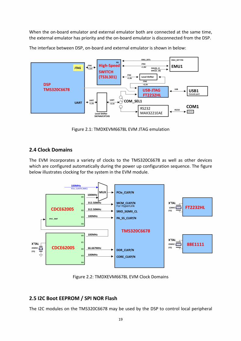
When the on-board emulator and external emulator both are connected at the same time,
the external emulator has priority and the on-board emulator is disconnected from the DSP.
The interface between DSP, on-board and external emulator is shown in below:
Figure 2.1: TMDXEVM6678L EVM JTAG emulation
2.4 Clock Domains
The EVM incorporates a variety of clocks to the TMS320C6678 as well as other devices
which are configured automatically during the power up configuration sequence. The figure
below illustrates clocking for the system in the EVM module.
Figure 2.2: TMDXEVM6678L EVM Clock Domains
2.5 I2C Boot EEPROM / SPI NOR Flash
The I2C modules on the TMS320C6678 may be used by the DSP to control local peripheral
COM1UART
RS232
MAX3221EAE
DSP TMS320C6678 USB1 USB-JTAG
FT2232HL
COM_SEL1
EMU_DET PIN EMU_DETz SEL
SWITCH (TS3L301)
EMU1 High-Speed +1.8V JTAG
JTAG
UART
Level Shifter
+3.3V JTAG
+1.8V JTAG
USB
+3.3V UART
+1.8V
+1.8V
RS232
Console port
SN74AVC4T245 Level Shifter
JTAG EMU[0..1]
EMU[2..18]
PRI_REF 100MHz
X'TAL 66.667MHz 25MHZ
CDCE62005
100MHz PCIe_CLKP/N (AMC)
(Y2)
(Y5)
X'TAL
(Y3)
TMS320C6678
X'TAL 12MHZ
25MHZ
312.50MHz
312.50MHz
100MHz
100MHz U0
U3
U2
U1
U4
U1
U0
CDCE62005
100MHz
U4
U3
U2
FT2232HL
88E1111
SRIO_SGMII_CL
PCIe_CLKP/N
MCM_CLKP/N For HyperLink
CORE_CLKP/N
PA_SS_CLKP/N
DDR_CLKP/N
MUX
20
ICs (DACs, ADCs, etc.) or may be used to communicate with other controllers in a system or
to implement a user interface.
The I2C bus is connected to one SEEPROM and to the 80-pin expansion header (TEST_PH1).
There are two banks in the I2C SEEPROM which respond separately at addresses 0x50 and
0x51. These banks can be loaded with demonstration programs. Currently, the bank at 0x50
contains the I2C boot code and PLL initialization procedure and the bank at 0x51 contains
the second level boot-loader program. The second level boot-loader can be used to run the
POST program or launch the OOB demonstration from NOR flash memory.
The serial peripheral interconnect (SPI) module provides an interface between the DSP and
other SPI-compliant devices. The primary intent of this interface is to allow for connection to
a SPI ROM for boot. The SPI module on TMS320C6678 is supported only in Master mode.
The NOR FLASH attached to CS0z on the TMS320C6678 is a NUMONYX N25Q128A21. This
NOR FLASH size is 16MB. It can contain demonstration programs such as POST or the OOB
demonstration.The CS1z of the SPI is used by the DSP to access registers within the FPGA.
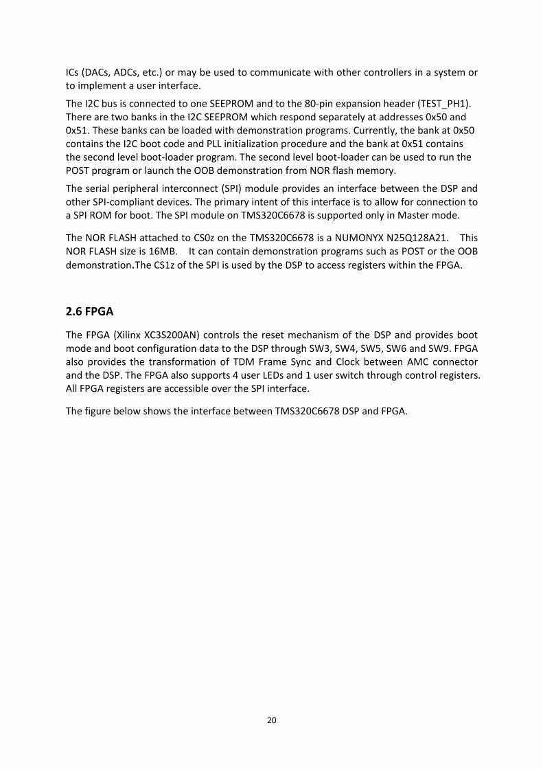
2.6 FPGA
The FPGA (Xilinx XC3S200AN) controls the reset mechanism of the DSP and provides boot
mode and boot configuration data to the DSP through SW3, SW4, SW5, SW6 and SW9. FPGA
also provides the transformation of TDM Frame Sync and Clock between AMC connector
and the DSP. The FPGA also supports 4 user LEDs and 1 user switch through control registers.
All FPGA registers are accessible over the SPI interface.
The figure below shows the interface between TMS320C6678 DSP and FPGA.
21
Figure 2.3: TMDXEVM6678L EVM FPGA Connections
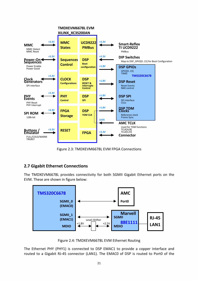
2.7 Gigabit Ethernet Connections
The TMDXEVM6678L provides connectivity for both SGMII Gigabit Ethernet ports on the
EVM. These are shown in figure below:
Figure 2.4: TMDXEVM6678L EVM Ethernet Routing
The Ethernet PHY (PHY1) is connected to DSP EMAC1 to provide a copper interface and
routed to a Gigabit RJ-45 connector (LAN1). The EMAC0 of DSP is routed to Port0 of the
PMBus UCD9222
Control Sequences
Configurations CLOCK
FPGA Storage
JTAG FPGA
Boot DSP
configuration
Control PHY
+3.3V +3.3V
TDM CLK
States MMC
Sequences
+3.3V
+3.3V
Power-On
Power Good Power Enable
Clock Generators
SPI interface
MMC Reset MMC Detect
+3.3V
PHY Interrupt PHY Reset
PHY Events
+3.3V
Buttons / +3.3V
128k-bit
TRGRST FULL/COLD/WARM
Emulator
PMBus
Smart-Reflex
+3.3V Map to DSP_GPIO[0..15] for Boot Configuration
DIP Switches
+1.8V
TIMI0 GPIO[0..15]
DSP GPIOs
Interrupts Control RESET & DSP
TMDXEVM6678L EVM XILINX_XC3S200AN
Reset Events DSP Reset +1.8V
+1.8V
NMI control
SPI interface DSP SPI
+1.8V CS1z
Clocks
Frame Sync. Reference clock
DSP TDM
AMC TCLKLVDS
TCLK[C/D] TCLK[A/B] Used for TDM functions
+3.3V Connector
TI UCD9222
RESET
MMC
TMS320C6678
DSP SPI
SPI ROM DSP
SGMII_0
(EMAC1)
SGMII_1
MDIO
TMS320C6678
Marvell
Port0
AMC
SGMII
MDIO88E1111
LAN1
RJ-45
(EMAC0)
Level-Shifter +1.8V +2.5V
22
AMC edge connector backplane interface.
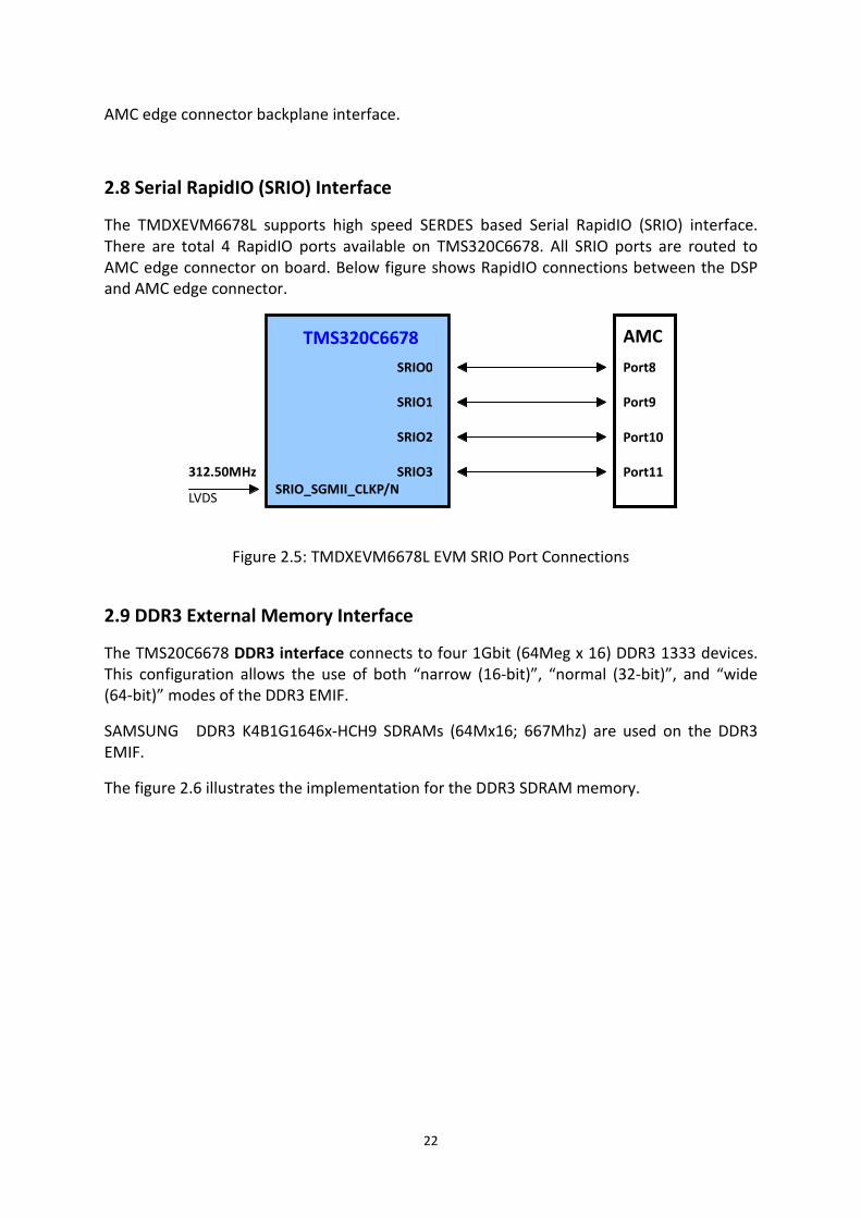
2.8 Serial RapidIO (SRIO) Interface
The TMDXEVM6678L supports high speed SERDES based Serial RapidIO (SRIO) interface.
There are total 4 RapidIO ports available on TMS320C6678. All SRIO ports are routed to
AMC edge connector on board. Below figure shows RapidIO connections between the DSP
and AMC edge connector.
Figure 2.5: TMDXEVM6678L EVM SRIO Port Connections
2.9 DDR3 External Memory Interface
The TMS20C6678 DDR3 interface connects to four 1Gbit (64Meg x 16) DDR3 1333 devices.
This configuration allows the use of both “narrow (16-bit)”, “normal (32-bit)”, and “wide
(64-bit)” modes of the DDR3 EMIF.
SAMSUNG DDR3 K4B1G1646x-HCH9 SDRAMs (64Mx16; 667Mhz) are used on the DDR3
EMIF.
The figure 2.6 illustrates the implementation for the DDR3 SDRAM memory.
SRIO0
TMS320C6678
Port8
AMC
Port9
Port11
Port10
SRIO3
SRIO2
SRIO1
312.50MHz SRIO_SGMII_CLKP/N
LVDS
23
Figure 2.6: TMDXEVM6678L EVM SDRAM
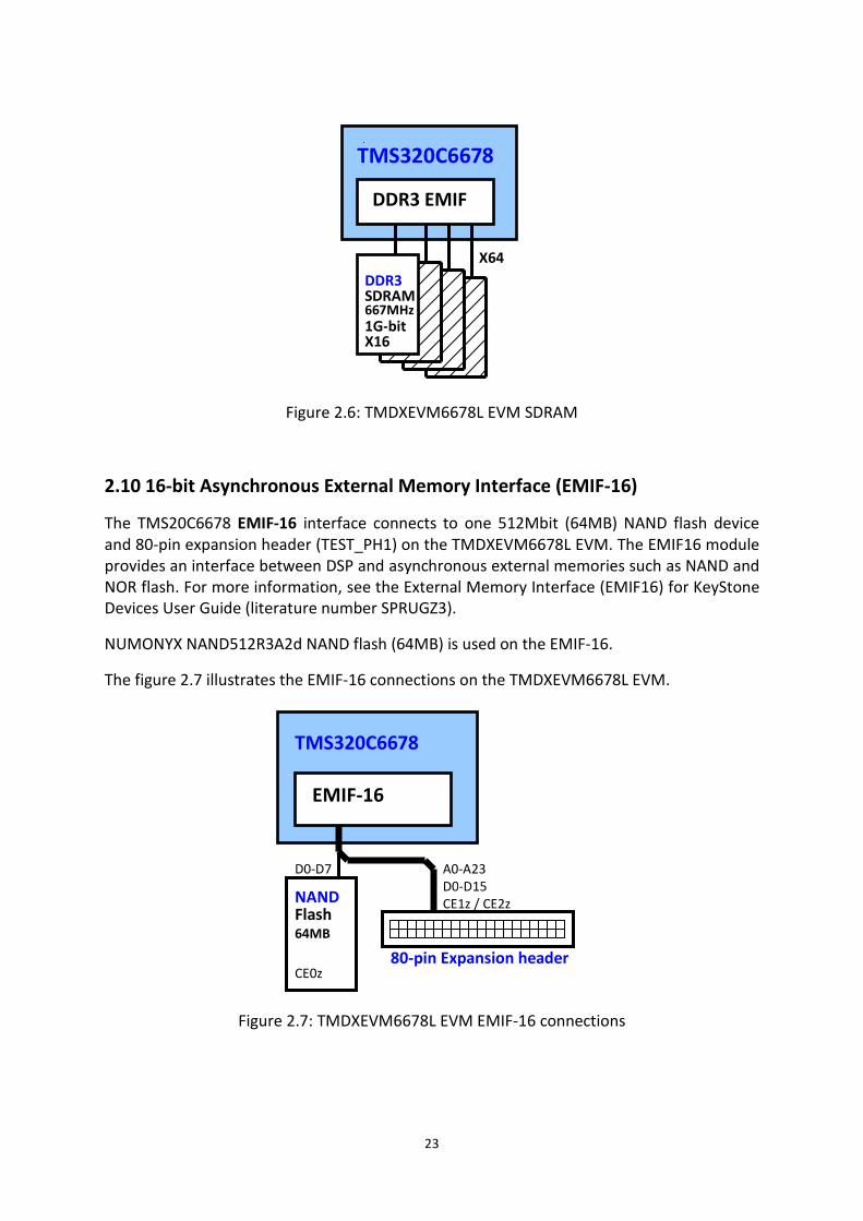
2.10 16-bit Asynchronous External Memory Interface (EMIF-16)
The TMS20C6678 EMIF-16 interface connects to one 512Mbit (64MB) NAND flash device
and 80-pin expansion header (TEST_PH1) on the TMDXEVM6678L EVM. The EMIF16 module
provides an interface between DSP and asynchronous external memories such as NAND and
NOR flash. For more information, see the External Memory Interface (EMIF16) for KeyStone
Devices User Guide (literature number SPRUGZ3).
NUMONYX NAND512R3A2d NAND flash (64MB) is used on the EMIF-16.
The figure 2.7 illustrates the EMIF-16 connections on the TMDXEVM6678L EVM.
Figure 2.7: TMDXEVM6678L EVM EMIF-16 connections
TMS320C6678
DDR3 EMIF
SDRAM
1G-bit
DDR3
667MHz
X64
X16
EMIF-16
TMS320C6678
CE0z
Flash NAND
64MB
CE1z / CE2z
A0-A23 D0-D15
D0-D7
80-pin Expansion header
24
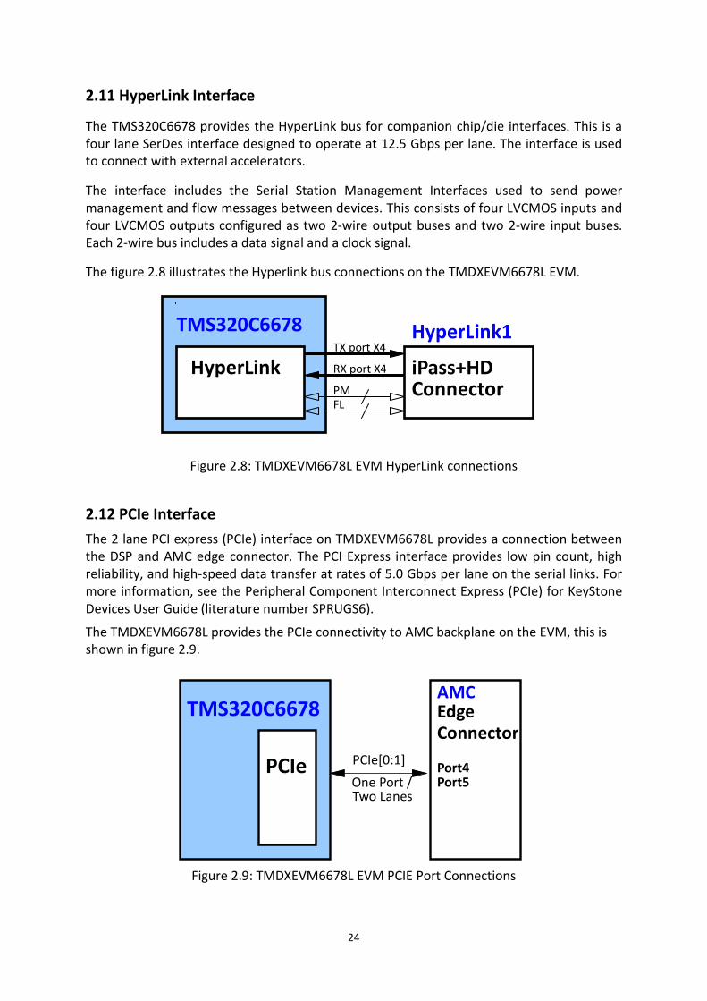
2.11 HyperLink Interface
The TMS320C6678 provides the HyperLink bus for companion chip/die interfaces. This is a
four lane SerDes interface designed to operate at 12.5 Gbps per lane. The interface is used
to connect with external accelerators.
The interface includes the Serial Station Management Interfaces used to send power
management and flow messages between devices. This consists of four LVCMOS inputs and
four LVCMOS outputs configured as two 2-wire output buses and two 2-wire input buses.
Each 2-wire bus includes a data signal and a clock signal.
The figure 2.8 illustrates the Hyperlink bus connections on the TMDXEVM6678L EVM.
Figure 2.8: TMDXEVM6678L EVM HyperLink connections
2.12 PCIe Interface
The 2 lane PCI express (PCIe) interface on TMDXEVM6678L provides a connection between
the DSP and AMC edge connector. The PCI Express interface provides low pin count, high
reliability, and high-speed data transfer at rates of 5.0 Gbps per lane on the serial links. For
more information, see the Peripheral Component Interconnect Express (PCIe) for KeyStone
Devices User Guide (literature number SPRUGS6).
The TMDXEVM6678L provides the PCIe connectivity to AMC backplane on the EVM, this is
shown in figure 2.9.
Figure 2.9: TMDXEVM6678L EVM PCIE Port Connections
PCIe
TMS320C6678 Edge
PCIe[0:1] Port4
Two Lanes One Port /
AMC
Connector
Port5
HyperLink
TMS320C6678
FL PM
RX port X4
TX port X4HyperLink1
Connector iPass+HD
25
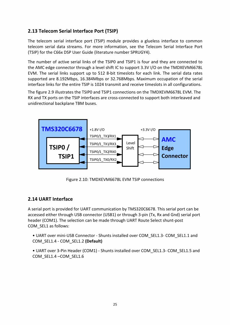
2.13 Telecom Serial Interface Port (TSIP)
The telecom serial interface port (TSIP) module provides a glueless interface to common
telecom serial data streams. For more information, see the Telecom Serial Interface Port
(TSIP) for the C66x DSP User Guide (literature number SPRUGY4).
The number of active serial links of the TSIP0 and TSIP1 is four and they are connected to
the AMC edge connector through a level shift IC to support 3.3V I/O on the TMDXEVM6678L
EVM. The serial links support up to 512 8-bit timeslots for each link. The serial data rates
supported are 8.192Mbps, 16.384Mbps or 32.768Mbps. Maximum occupation of the serial
interface links for the entire TSIP is 1024 transmit and receive timeslots in all configurations.
The figure 2.9 illustrates the TSIP0 and TSIP1 connections on the TMDXEVM6678L EVM. The
RX and TX ports on the TSIP interfaces are cross-connected to support both interleaved and
unidirectional backplane TBM buses.
Figure 2.10: TMDXEVM6678L EVM TSIP connections
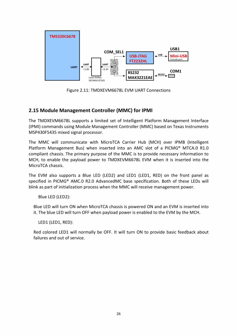
2.14 UART Interface
A serial port is provided for UART communication by TMS320C6678. This serial port can be
accessed either through USB connector (USB1) or through 3-pin (Tx, Rx and Gnd) serial port
header (COM1). The selection can be made through UART Route Select shunt-post
COM_SEL1 as follows:
• UART over mini-USB Connector - Shunts installed over COM_SEL1.3- COM_SEL1.1 and
COM_SEL1.4 - COM_SEL1.2 (Default)
• UART over 3-Pin Header (COM1) - Shunts installed over COM_SEL1.3- COM_SEL1.5 and
COM_SEL1.4 –COM_SEL1.6
TSIP0 /
TMS320C6678
AMC
Connector
Edge
TSIP1
+3.3V I/O +1.8V I/O
TSIP0/1_TX3/RX1
Shift Level
TSIP0/1_TX0/RX2
TSIP0/1_TX2/RX0
TSIP0/1_TX1/RX3
26
Figure 2.11: TMDXEVM6678L EVM UART Connections
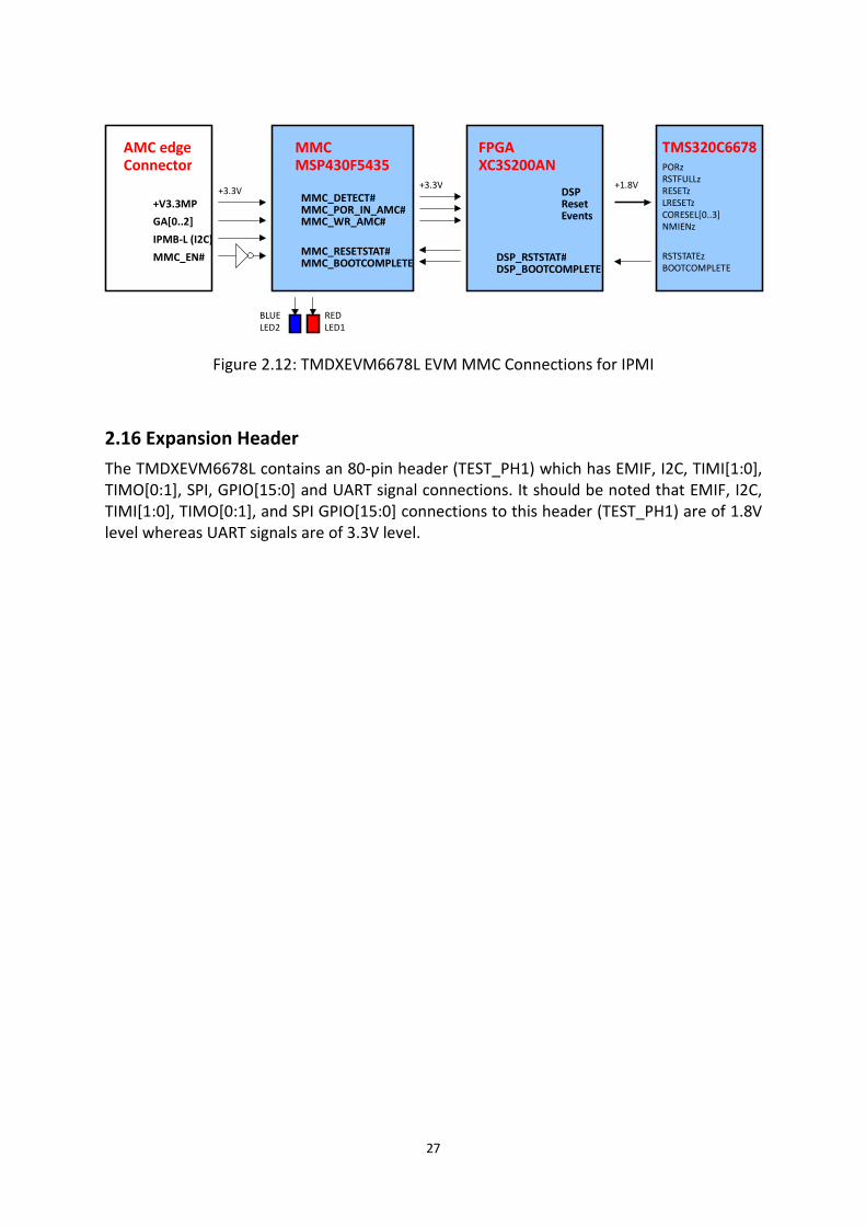
2.15 Module Management Controller (MMC) for IPMI
The TMDXEVM6678L supports a limited set of Intelligent Platform Management Interface
(IPMI) commands using Module Management Controller (MMC) based on Texas Instruments
MSP430F5435 mixed signal processor.
The MMC will communicate with MicroTCA Carrier Hub (MCH) over IPMB (Intelligent
Platform Management Bus) when inserted into an AMC slot of a PICMG® MTCA.0 R1.0
compliant chassis. The primary purpose of the MMC is to provide necessary information to
MCH, to enable the payload power to TMDXEVM6678L EVM when it is inserted into the
MicroTCA chassis.
The EVM also supports a Blue LED (LED2) and LED1 (LED1, RED) on the front panel as
specified in PICMG® AMC.0 R2.0 AdvancedMC base specification. Both of these LEDs will
blink as part of initialization process when the MMC will receive management power.
Blue LED (LED2):
Blue LED will turn ON when MicroTCA chassis is powered ON and an EVM is inserted into
it. The blue LED will turn OFF when payload power is enabled to the EVM by the MCH.
LED1 (LED1, RED):
Red colored LED1 will normally be OFF. It will turn ON to provide basic feedback about
failures and out of service.
UART COM1RS232
MAX3221EAE
TMS320C6678
USB-JTAG
FT2232HL
Mini-USB COM_SEL1
UART
USB
+3.3V UART
+1.8V
RS232
Console port
USB1
SN74AVC4T245 Level Shifter
27
Figure 2.12: TMDXEVM6678L EVM MMC Connections for IPMI
2.16 Expansion Header
The TMDXEVM6678L contains an 80-pin header (TEST_PH1) which has EMIF, I2C, TIMI[1:0],
TIMO[0:1], SPI, GPIO[15:0] and UART signal connections. It should be noted that EMIF, I2C,
TIMI[1:0], TIMO[0:1], and SPI GPIO[15:0] connections to this header (TEST_PH1) are of 1.8V
level whereas UART signals are of 3.3V level.
GA[0..2]
AMC edge
+3.3V
IPMB-L (I2C)
MMC_POR_IN_AMC# MMC_DETECT#
Connector
+V3.3MP
MMC_EN#
MSP430F5435 MMC
MMC_BOOTCOMPLETE
MMC_WR_AMC#
MMC_RESETSTAT#
XC3S200AN FPGA
+3.3V
Events Reset DSP +1.8V
TMS320C6678
DSP_BOOTCOMPLETEDSP_RSTSTAT#
NMIENz CORESEL[0..3] LRESETz RESETz RSTFULLz
BOOTCOMPLETE RSTSTATEz
LED2 BLUE RED
LED1
PORz
28
3. TMDXEVM6678L Board Physical Specifications
This chapter describes the physical layout of the TMDXEVM6678L board and its connectors,
switches and test points. It contains:
3.1 Board Layout
3.2 Connector Index
3.3 Switches
3.4 Test Points
3.5 System LEDs
3.1 Board Layout
The TMDXEVM6678L board dimension is 7.11” x 2.89” (180.6mm x 73.5mm). It is a 12-layer
board and powered through connector DC_IN1. Figure 3-1 and 3-2 shows assembly layout of
the TMDXEVM6678L EVM Board.
Figure 3.1: TMDXEVM6678L EVM Board Assembly Layout – TOP view
29
Figure 3.2: TMDXEVM6678L EVM Board layout – Bottom view
3.2 Connector Index
The TMDXEVM6678L Board has several connectors which provide access to various
interfaces on the board.
Table 3.1 : TMDXEVM6678L EVM Board Connectors
Connector Pins Function
560V2_PWR1 8 XDS560v2 Mezzanine Power Connector
AMC1 170 AMC Edge Connector
COM1 3 UART 3-Pin Connector
COM_SEL1 6 UART Route Select Jumper
DC_IN1 3 DC Power Input Jack Connector
EMU1 60 TI 60-Pin DSP JTAG Connector
FAN1 3 FAN connector for +12V DC FAN
HyperLink1 36 HyperLink connector for companion chip/die
interface
LAN1 12 Gigabit Ethernet RJ-45 Connector
PMBUS1 5 PMBUS for Smart-Reflex connected to UCD9222
TAP_FPGA1 10 FPGA JTAG Connector
TAP_MMC1 14 MSP430 JTAG Connector -- For Factory Use Only
TEST_PH1 80 EMIF, SPI, I2C, GPIO, TIMI[1:0], TIMO[1:0], and
UART1 connections
USB1 5 Mini-USB Connector
3.2.1 560V2_PWR1, XDS560v2 Mezzanine Power Connector
560V2_PWR1 is an 8-pin power connector for XDS560v2 mezzanine emulator board. The
pin out for the connector is shown in the figure below:
30
Table 3.2 : XDS560v2 Power Connector pin out
Pin # Signal Name
1 +5VSupply
2 +5VSupply
3 XDS560V2_IL
4 Ground
5 +3.3VSupply
6 +3.3VSupply
7 Ground
8 Ground
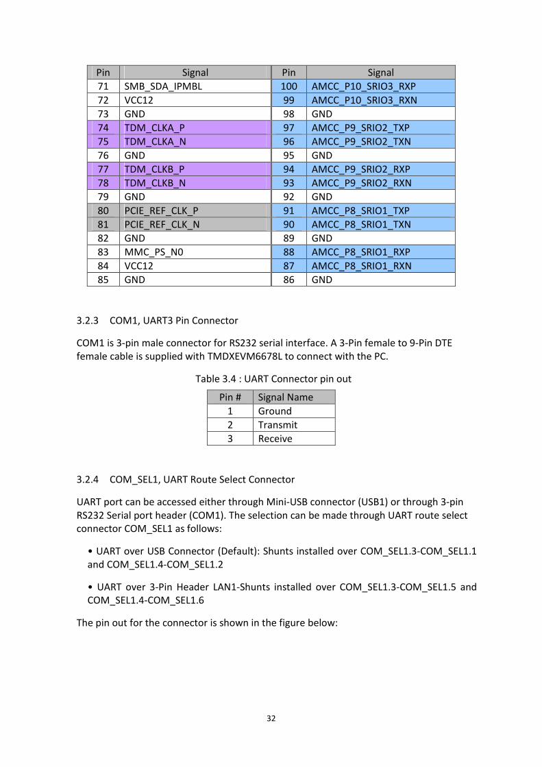
3.2.2 AMC1, AMC Edge Connector
The AMC card edge connector plugs into an AMC compatible carrier board and provides 4
Serial RapidIO lanes, 2 PCIe lanes, 1 SGMII port, 2 4-lane TDM ports and system interfaces
to the carrier board. This connector is the 170 pin B+ style. The signals on this connector
are shown in the table below:
Table 3.3: AMC Edge Connector
Pin Signal Pin Signal
1 GND 170 GND
2 VCC12 169 NC
3 MMC_PS_N1# 168 NC
4 VCC3V3_MP_AMC 167 NC
5 MMC_GA0 166 NC
6 RSVD 165 NC
7 GND 164 GND
8 RSVD 163 NC
9 VCC12 162 NC
10 GND 161 GND
11 AMC0_SGMII0_TX_DP 160 NC
12 AMC0_SGMII0_TX_DP 159 NC
13 GND 158 GND
14 AMC0_SGMII0_RX_DP 157 NC
15 AMC0_SGMII0_RX_DN 156 NC
16 GND 155 GND
17 MMC_GA1 154 NC
18 VCC12 153 NC
19 GND 152 GND
20 NC 151 NC
21 NC 150 NC
22 GND 149 GND
23 NC 148 NC
24 NC 147 NC
25 GND 146 GND
31
Pin Signal Pin Signal
26 MMC_GA2 145 NC
27 VCC12 144 NC
28 GND 143 GND
29 NC 142 NC
30 NC 141 NC
31 GND 140 GND
32 NC 139 TDM_CLKD_P
33 NC 138 TDM_CLKD_N
34 GND 137 GND
35 NC 136 TDM_CLKC_P
36 NC 135 TDM_CLKC_N
37 GND 134 GND
38 NC 133 NC
39 NC 132 NC
40 GND 131 GND
41 MMC_ENABLE_N 130 DSP_SDA_AMC
42 VCC12 129 DSP_SCL_AMC
43 GND 128 GND
44 AMCC_P4_PCIe_TX1P 127 NC
45 AMCC_P4_PCIe_TX1N 126 NC
46 GND 125 GND
47 AMCC_P4_PCIe_RX1P 124 NC
48 AMCC_P4_PCIe_RX1N 123 NC
49 GND 122 GND
50 AMCC_P5_PCIe_TX2P 121 AMCC_P13_TDM1_TX3/RX1
51 AMCC_P5_PCIe_TX2N 120 AMCC_P13_TDM1_TX1/RX3
52 GND 119 GND
53 AMCC_P5_PCIe_RX2P 118 AMCC_P13_TDM1_TX2/RX0
54 AMCC_P5_PCIe_RX2N 117 AMCC_P13_TDM1_TX0/RX2
55 GND 116 GND
56 SMB_SCL_IPMBL 115 AMCC_P12_TDM0_TX3/RX1
57 VCC12 114 AMCC_P12_TDM0_TX1/RX3
58 GND 113 GND
59 NC 112 AMCC_P12_TDM0_TX2/RX0
60 NC 111 AMCC_P12_TDM0_TX0/RX2
61 GND 110 GND
62 NC 109 AMCC_P11_SRIO4_TXP
63 NC 108 AMCC_P11_SRIO4_TXN
64 GND 107 GND
65 NC 106 AMCC_P11_SRIO4_RXP
66 NC 105 AMCC_P11_SRIO4_RXN
67 GND 104 GND
68 NC 103 AMCC_P10_SRIO3_TXP
69 NC 102 AMCC_P10_SRIO3_TXN
70 GND 101 GND
32
Pin Signal Pin Signal
71 SMB_SDA_IPMBL 100 AMCC_P10_SRIO3_RXP
72 VCC12 99 AMCC_P10_SRIO3_RXN
73 GND 98 GND
74 TDM_CLKA_P 97 AMCC_P9_SRIO2_TXP
75 TDM_CLKA_N 96 AMCC_P9_SRIO2_TXN
76 GND 95 GND
77 TDM_CLKB_P 94 AMCC_P9_SRIO2_RXP
78 TDM_CLKB_N 93 AMCC_P9_SRIO2_RXN
79 GND 92 GND
80 PCIE_REF_CLK_P 91 AMCC_P8_SRIO1_TXP
81 PCIE_REF_CLK_N 90 AMCC_P8_SRIO1_TXN
82 GND 89 GND
83 MMC_PS_N0 88 AMCC_P8_SRIO1_RXP
84 VCC12 87 AMCC_P8_SRIO1_RXN
85 GND 86 GND
3.2.3 COM1, UART3 Pin Connector
COM1 is 3-pin male connector for RS232 serial interface. A 3-Pin female to 9-Pin DTE
female cable is supplied with TMDXEVM6678L to connect with the PC.
Table 3.4 : UART Connector pin out
Pin # Signal Name
1 Ground
2 Transmit
3 Receive
3.2.4 COM_SEL1, UART Route Select Connector
UART port can be accessed either through Mini-USB connector (USB1) or through 3-pin
RS232 Serial port header (COM1). The selection can be made through UART route select
connector COM_SEL1 as follows:
• UART over USB Connector (Default): Shunts installed over COM_SEL1.3-COM_SEL1.1
and COM_SEL1.4-COM_SEL1.2
• UART over 3-Pin Header LAN1-Shunts installed over COM_SEL1.3-COM_SEL1.5 and
COM_SEL1.4-COM_SEL1.6
The pin out for the connector is shown in the figure below:
33
Table 3.5 : UART Path Select Connector pin out
Pin # Signal Name Pin # Signal Name
1 FT2232H (USB Chip)
Transmit 2
FT2232H (USB Chip)
Receive
3 UART Transmit 4 UART Receive
5 MAX3221 Transmit 6 MAX3221 Receive
3.2.5 DC_IN1, DC Power Input Jack Connector
DC_IN1 is a DC Power-in Jack Connector for the stand-alone application of
TMDXEVM6678L. It is a 2.5mm power jack with positive center tip polarity. Do not use
this connector if EVM is inserted into MicroTCA chassis or AMC carrier backplane.
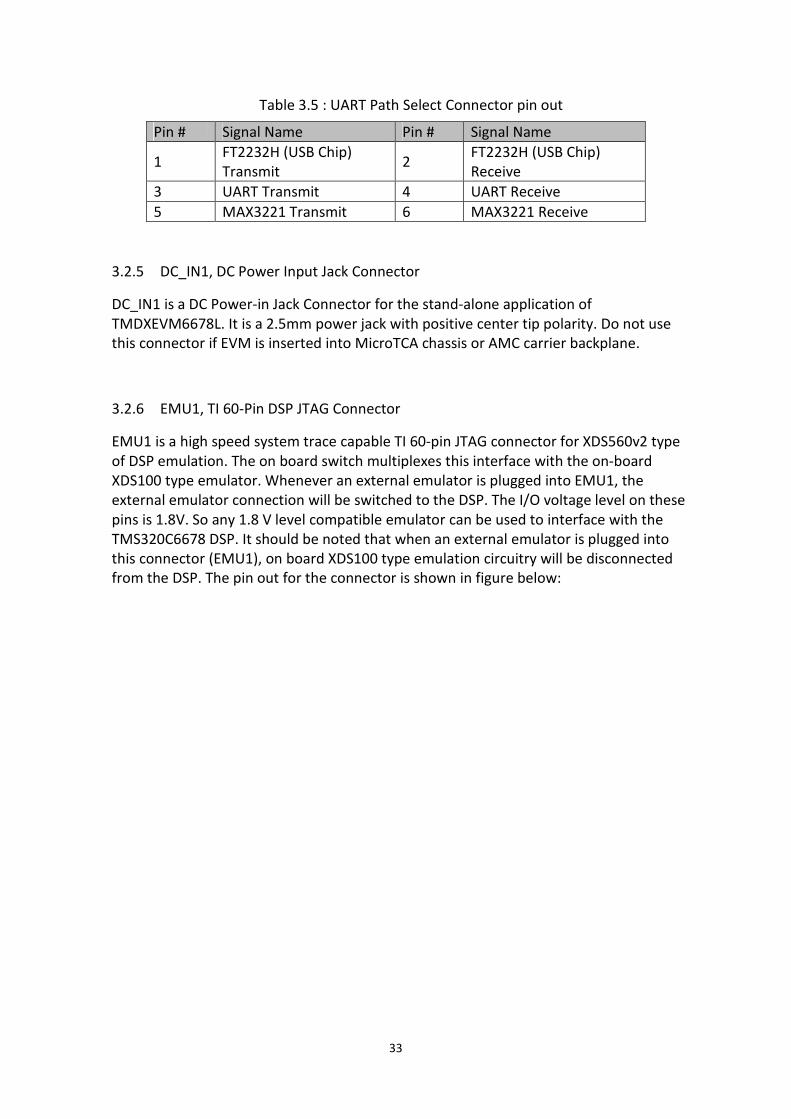
3.2.6 EMU1, TI 60-Pin DSP JTAG Connector
EMU1 is a high speed system trace capable TI 60-pin JTAG connector for XDS560v2 type
of DSP emulation. The on board switch multiplexes this interface with the on-board
XDS100 type emulator. Whenever an external emulator is plugged into EMU1, the
external emulator connection will be switched to the DSP. The I/O voltage level on these
pins is 1.8V. So any 1.8 V level compatible emulator can be used to interface with the
TMS320C6678 DSP. It should be noted that when an external emulator is plugged into
this connector (EMU1), on board XDS100 type emulation circuitry will be disconnected
from the DSP. The pin out for the connector is shown in figure below:
34
Table 3.6: DSP JTAG Connector pin out
Pin # Signal Name Pin # Signal Name
A1 Ground C1 ID2 (GND)
A2 Ground C2 EMU18
A3 Ground C3 TRST#
A4 Ground C4 EMU16
A5 Ground C5 EMU15
A6 Ground C6 EMU13
A7 Ground C7 EMU11
A8 Type0 (NC) C8 TCLKRTN
A9 Ground C9 EMU10
A10 Ground C10 EMU8
A11 Ground C11 EMU6
A12 Ground C12 EMU4
A13 Ground C13 EMU3
A14 Ground C14 EMU1
A15 TRGRST# C15 ID3 (GND)
B1 ID0 (GND) D1 NC
B2 TMS D2 Ground
B3 EMU17 D3 Ground
B4 TDI D4 Ground
B5 EMU14 D5 Ground
B6 EMU12 D6 Ground
B7 TDO D7 Ground
B8 TVD (+1.8V) D8 Type1 (GND)
B9 EMU9 D9 Ground
B10 EMU7 D10 Ground
B11 EMU5 D11 Ground
B12 TCLK D12 Ground
B13 EMU2 D13 Ground
B14 EMU0 D14 Ground
B15 ID1 (GND) D15 Ground
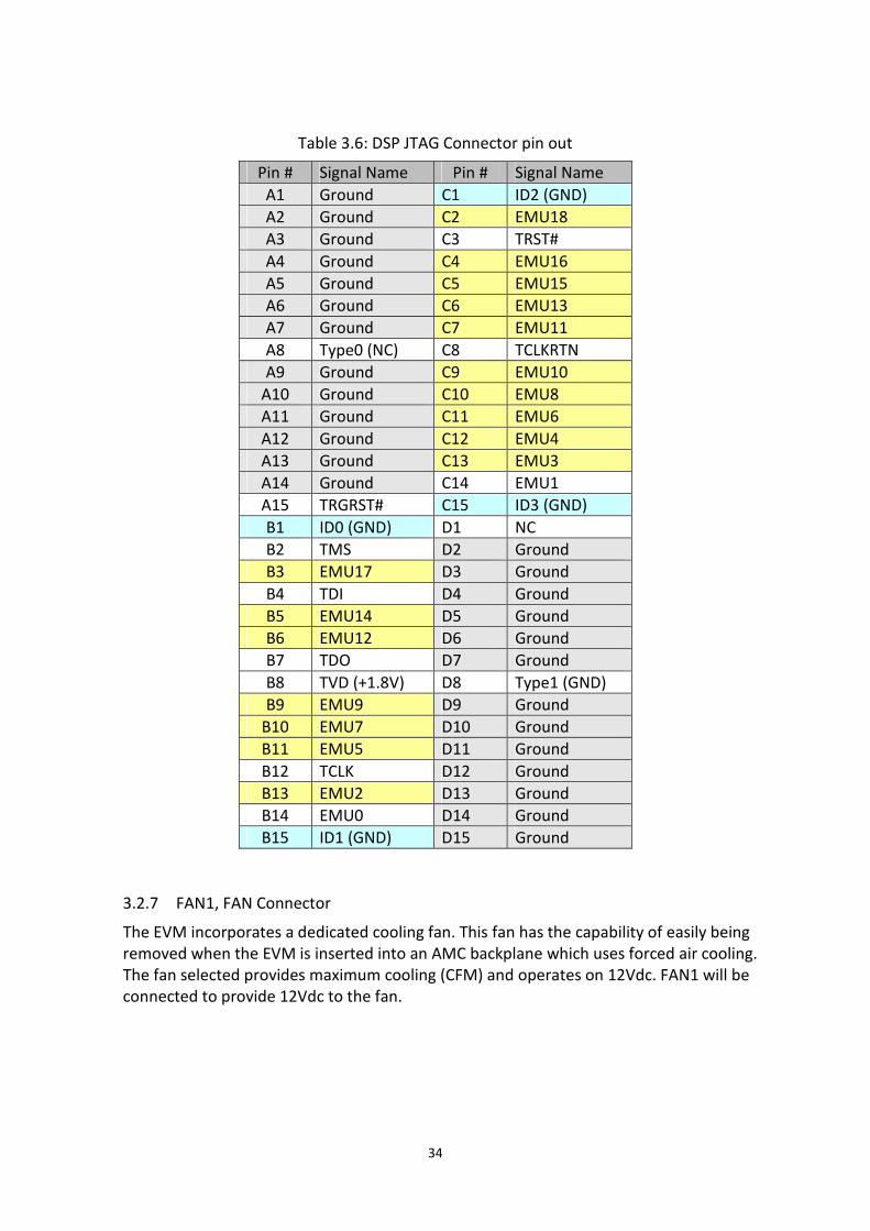
3.2.7 FAN1, FAN Connector
The EVM incorporates a dedicated cooling fan. This fan has the capability of easily being
removed when the EVM is inserted into an AMC backplane which uses forced air cooling.
The fan selected provides maximum cooling (CFM) and operates on 12Vdc. FAN1 will be
connected to provide 12Vdc to the fan.
35
Table 3.7 : FAN1 Connector pin out
Pin # Signal Name
1 GNG
2 +12Vdc
3 NC
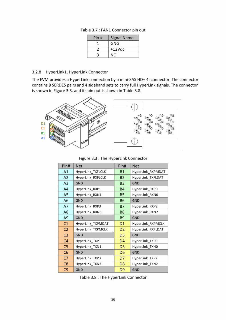
3.2.8 HyperLink1, HyperLink Connector
The EVM provides a HyperLink connection by a mini-SAS HD+ 4i connector. The connector
contains 8 SERDES pairs and 4 sideband sets to carry full HyperLink signals. The connector
is shown in Figure 3.3. and its pin out is shown in Table 3.8.
Figure 3.3 : The HyperLink Connector
Pin# Net Pin# Net
A1 HyperLink_TXFLCLK B1 HyperLink_RXPMDAT
A2 HyperLink_RXFLCLK B2 HyperLink_TXFLDAT
A3 GND B3 GND
A4 HyperLink_RXP1 B4 HyperLink_RXP0
A5 HyperLink_RXN1 B5 HyperLink_RXN0
A6 GND B6 GND
A7 HyperLink_RXP3 B7 HyperLink_RXP2
A8 HyperLink_RXN3 B8 HyperLink_RXN2
A9 GND B9 GND
C1 HyperLink_TXPMDAT D1 HyperLink_RXPMCLK
C2 HyperLink_TXPMCLK D2 HyperLink_RXFLDAT
C3 GND D3 GND
C4 HyperLink_TXP1 D4 HyperLink_TXP0
C5 HyperLink_TXN1 D5 HyperLink_TXN0
C6 GND D6 GND
C7 HyperLink_TXP3 D7 HyperLink_TXP2
C8 HyperLink_TXN3 D8 HyperLink_TXN2
C9 GND D9 GND
Table 3.8 : The HyperLink Connector
A1
B1
C1
D1
36
3.2.9 LAN1, Ethernet Connector
LAN1 is a Gigabit RJ45 Ethernet connector with integrated magnetics. It is driven by
Marvell Gigabit Ethernet transceiver 88E1111. The connections are shown in the table
below:
Table 3.9 : Ethernet Connector pin out
Pin # Signal Name
1 Center Tap2
2 MD2-
3 MD2+
4 MD1-
5 MD1+
6 Center Tap1
7 Center Tap3
8 MD3+
9 MD3-
10 MD0-
11 MD0+
12 Center Tap0
13 ACT_LED1-
14 ACT_LED1+
15 LINK1000_LED2-
16 LINK_LED2+
17 LINK100_LED2-
H3 Shield 1
H4 Shield 2
3.2.10 PMBUS1, PMBUS Connector for Smart-Reflex Control
The TMS320C6678 DSP core power is supplied by a Smart-Reflex power controller
UCD9222 with the Integrated FET Driver UCD7242. PMBUS1 provides a connection
between UCD9222 and remote connection during development. Through the USB to GPIO
pod provided by TI, the user can trace and configure the parameters in UCD9222 with the
Smart-Fusion GUI. The pin out of PMBUS1 is shown in table 3.10.
Table 3.10 : PMBUS1 pin out
Pin # Signal Name
1 VCC3V3_AUX
2 PMBUS_CLK
3 PMBUS_DAT
4 PMBUS_ALT
5 PMBUS_CTL
6 GND
37
3.2.11 TAP_FPGA1, FPGA JTAG Connector (For Factory Use Only)
TAP_FPGA1 is an 8-pin JTAG connector for the FPGA programming and the PHY boundary
test of the factory only. The pin out for the connector is shown in the figure below:
Table 3.11 : FPGA JTAG Connector pin out
Pin # Signal Name
1 VCC3V3_FPGA
2 GND
3 BSC_JTAG_TCK
4 BSC_JTAG_RST#
5 BSC_JTAG_TDO
6 BSC_JTAG_TDI
7 BSC_JTAG_TMS
8 NC
The diagram of the boundary scan route is shown in Figure 3.4.
Figure 3.4 : TAP_FPGA1 function diagram
3.2.12 TAP_MMC1, MSP430 JTAG Connector (For Factory Use Only)
TAP_MMC1 is a 14-pin JTAG connector for IPMI software loading into MSP430. The
TMDXEVM6678L are supplied with IPMI software already loaded into MSP430. The pin
out for the connector is shown in the figure below:
TDO
TDI TDO TDI TDO
TDI
TAP_FPGA1
JTAG
FPGA XC3S200AN
JTAG
Gigabit PHY
Boundary Scan
Diagram
TMS/TCK/TRSTn
(88E1111)
38
Table 3.12 : MSP430 JTAG Connector pin out
Pin # Signal Name Pin # Signal Name
1 MMC_TDO 2 VCCTOOL(NC)
3 MMC_TDI 4 VCC
5 MMC_TMS 6 NC (Key)
7 MMC_TCK 8 MMC_TEST
9 GND 10 NC
11 MMC_RST_N 12 NC
13 NC 14 NC
3.2.13 TEST_PH1, Expansion Header (EMIF-16, SPI, GPIO, Timer I/O, I2C, and UART)
TEST_PH1 is an expansion header for several interfaces on the DSP. They are 16-bit EMIF,
SPI, GPIO, Timer, I2C, and UART. The signal connections to the test header are as shown in
a table below:
Table 3.13 : Test Header pin out
Pin Signal Description Pin Signal Description
1 GND Ground 2 DSP_EMIFA00 EMIF addr0
3 DSP_SDA DSP I2C data 4 DSP_EMIFA01 EMIF addr1
5 DSP_SCL DSP I2C clock 6 DSP_EMIFA02 EMIF addr2
7 DSP_EMIFD0 EMIF data0 8 DSP_EMIFA03 EMIF addr3
9 DSP_EMIFD1 EMIF data1 10 DSP_EMIFA04 EMIF addr4
11 DSP_EMIFD2 EMIF data2 12 DSP_EMIFA05 EMIF addr5
13 DSP_EMIFD3 EMIF data3 14 DSP_EMIFA06 EMIF addr6
15 DSP_EMIFD4 EMIF data4 16 DSP_EMIFA07 EMIF addr7
17 DSP_EMIFD5 EMIF data5 18 DSP_EMIFA08 EMIF addr8
19 DSP_EMIFD6 EMIF data6 20 DSP_EMIFA09 EMIF addr9
21 DSP_EMIFD7 EMIF data7 22 DSP_EMIFA10 EMIF addr10
23 DSP_EMIFD8 EMIF data8 24 DSP_EMIFA11 EMIF addr11
25 DSP_EMIFD9 EMIF data9 26 DSP_EMIFA12 EMIF addr12
27 DSP_EMIFD10 EMIF data10 28 DSP_EMIFA13 EMIF addr13
29 DSP_EMIFD11 EMIF data11 30 DSP_EMIFA14 EMIF addr14
31 DSP_EMIFD12 EMIF data12 32 DSP_EMIFA15 EMIF addr15
33 DSP_EMIFD13 EMIF data13 34 DSP_EMIFA16 EMIF addr16
35 DSP_EMIFD14 EMIF data14 36 DSP_EMIFA17 EMIF addr17
39
Pin Signal Description Pin Signal Description
37 DSP_EMIFD15 EMIF data15 38 DSP_EMIFA18 EMIF addr18
39 DSP_EMIFCE1z EMIF Space Enable1 40 DSP_EMIFA19 EMIF addr19
41 DSP_EMIFCE2z EMIF Space Enable2 42 DSP_EMIFA20 EMIF addr20
43 DSP_EMIFBE0z EMIF Byte Enable0 44 DSP_EMIFA21 EMIF addr21
45 DSP_EMIFBE1z EMIF Byte Enable1 46 DSP_EMIFA22 EMIF addr22
47 DSP_EMIFOEz EMIF Output Enable 48 DSP_EMIFA23 EMIF addr23
49 DSP_EMIFWEz EMIF Write Enable 50 DSP_GPIO_00 DSP GPIO0
51 DSP_EMIFRNW EMIF Read/Write 52 DSP_GPIO_01 DSP GPIO1
53 DSP_EMIFWAIT1 EMIF Wait 54 DSP_GPIO_02 DSP GPIO2
55 DSP_TIMI0 Timer input 0 56 DSP_GPIO_03 DSP GPIO3
57 DSP_TIMO0 Timer output 0 58 DSP_GPIO_04 DSP GPIO4
59 DSP_TIMI1 Timer input 1 60 DSP_GPIO_05 DSP GPIO5
61 DSP_TIMO1 Timer output 1 62 DSP_GPIO_06 DSP GPIO6
63 DSP_SSPMISO SPI data input 64 DSP_GPIO_07 DSP GPIO7
65 DSP_SSPMOSI SPI data output 66 DSP_GPIO_08 DSP GPIO8
67 DSP_SSPCS1 SPI chip select 68 DSP_GPIO_09 DSP GPIO9
69 PH_SSPCK SPI clock 70 DSP_GPIO_10 DSP GPIO10
71 DSP_UARTTXD UART Serial Data Out
(+3.3v) 72 DSP_GPIO_11 DSP GPIO11
73 DSP_UARTRXD UART Serial Data In
(+3.3v) 74 DSP_GPIO_12 DSP GPIO12
75 DSP_UARTRTS UART Request To
Send (+3.3v) 76 DSP_GPIO_13 DSP GPIO13
77 DSP_UARTCTS UART Cear To Send
(+3.3v) 78 DSP_GPIO_14 DSP GPIO14
79 GND Ground 80 DSP_GPIO_15 DSP GPIO15
3.2.14 USB1, Mini-USB Connector
USB1 is a 5-pin Mini-USB connector to connect Code Composer Studio with
TMS320C6678 DSP using XDS100 type on-board emulation circuitry. Below table shows
the pin outs of the Mini-USB connector.
40
Table 3.14 : Mini-USB Connector pin out
Pin # Signal Name
1 VBUS
2 USB D-
3 USB D+
4 ID (NC)
5 Ground
3.3 DIP and Pushbutton Switches
The TMDXEVM6678L has 3 push button switches and five sliding actuator DIP switches. The
RST_FULL1, RST_COLD1, and RST_WARM1 are push button switches while SW3, SW4, SW5,
SW6 and SW9 are DIP switches. The function of each of the switches is listed in the table
below:
Table 3.15 : TMDXEVM6678L EVM Board Switches
Switch Function
RST_FULL1 Full Reset Event
RST_COLD1 Cold Reset Event (RFU)
RST_WARM1 Warm Reset Event
SW3 DSP Boot mode, DSP Configuration
SW4 DSP boot Configuration
SW5 DSP boot Configuration
SW6 DSP boot Configuration, PLL
setting, PCIe mode Selection
SW9 PCIe Enable/Disable, User Switch
3.3.1 RST_FULL1, Full Reset
Pressing the RST_FULL1 button switch will issue a RESETFULL# to TMS320C6678 by the
FPGA. It’ll reset DSP and other peripherals.
3.3.2 RST_COLD1, Cold Reset
The button is reserved for future use.
3.3.3 RST_WARM1, Warm Reset
Pressing the RST_WARM1 button switch will issue a RESET# to TMS320C6678 by the FPGA.
The FPGA will assert the RESET# signal to the DSP and the DSP will execute either a HARD
or SOFT reset by the configuration in the RSCFG register in PLLCTL.
Note: Users may refer to the TMS320C6678 Data Manual to check the difference between
assertion of DSP RESET# and the other reset signals.
3.3.4 SW3, SW4, SW5, and SW6, DSP boot mode and Configuration
SW3, SW4, SW5, and SW6 are 4-position DIP switches, which are used for DSP ENDIAN,
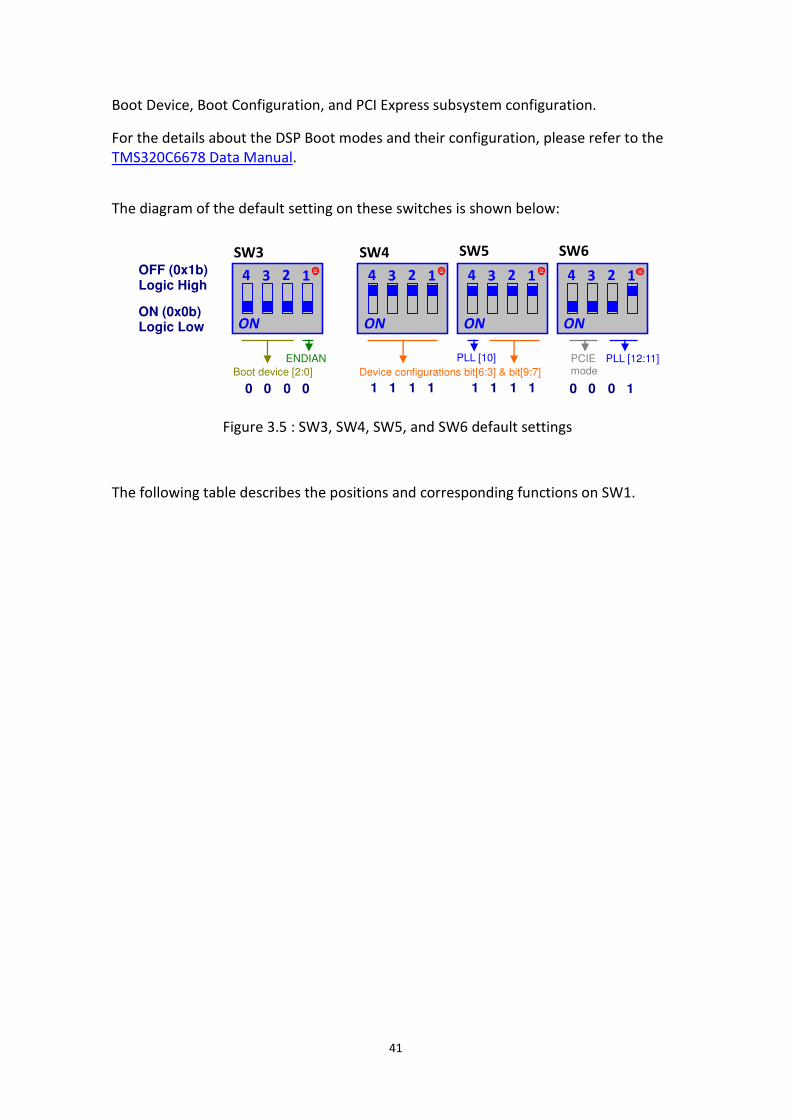
41
Boot Device, Boot Configuration, and PCI Express subsystem configuration.
For the details about the DSP Boot modes and their configuration, please refer to the
TMS320C6678 Data Manual.
The diagram of the default setting on these switches is shown below:
Figure 3.5 : SW3, SW4, SW5, and SW6 default settings
The following table describes the positions and corresponding functions on SW1.
ON
3 24 13 24 1
ON
3 24 1
ON
3
SW6 SW5 SW4 SW3
2 4 1 OFF (0x1b) Logic High
ON (0x0b) Logic Low
0 0 0 0 1 1 1 1 1 1 1 1 0 0 0 1
ENDIAN
Boot device [2:0] Device configurations bit[6:3] & bit[9:7]
ON
PLL [10] PCIE mode
PLL [12:11]
42
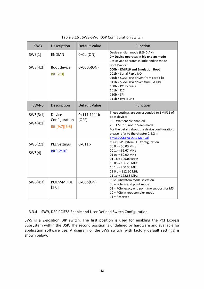
Table 3.16 : SW3-SW6, DSP Configuration Switch
SW3 Description Default Value Function
SW3[1] ENDIAN 0x0b (ON) Device endian mode (LENDIAN).
0 = Device operates in big endian mode
1 = Device operates in little endian mode
SW3[4:2] Boot device
Bit [2:0]
0x000b(ON) Boot Device
000b = EMIF16 and Emulation Boot
001b = Serial Rapid I/O
010b = SGMII (PA driven from core clk)
011b = SGMII (PA driver from PA clk)
100b = PCI Express
101b = I2C
110b = SPI
111b = HyperLink
SW4-6 Description Default Value Function
SW5[3:1]
SW4[4:1]
Device
Configuration
Bit [9:7][6:3]
0x111 1111b
(OFF)
These settings are corresponded to EMIF16 of
boot device:
1. Wait enable enabled,
2. EMIF16, not in Sleep mode.
For the details about the device configuration,
please refer to the chapter 2.5.2 in
TMS320C6678 Data Manual.
SW6[2:1]
SW5[4]
PLL Settings
Bit[12:10]
0x011b C66x DSP System PLL Configuration
00 0b = 50.00 MHz
00 1b = 66.67 MHz
01 0b = 80.00 MHz
01 1b = 100.00 MHz
10 0b = 156.25 MHz
10 1b = 250.00 MHz
11 0 b = 312.50 MHz
11 1b = 122.88 MHz
SW6[4:3] PCIESSMODE
[1:0]
0x00b(ON) PCIe Subsystem mode selection.
00 = PCIe in end point mode
01 = PCIe legacy end point (no support for MSI)
10 = PCIe in root complex mode
11 = Reserved
3.3.4 SW9, DSP PCIESS Enable and User Defined Switch Configuration
SW9 is a 2-position DIP switch. The first position is used for enabling the PCI Express
Subsystem within the DSP. The second position is undefined by hardware and available for
application software use. A diagram of the SW9 switch (with factory default settings) is
shown below:
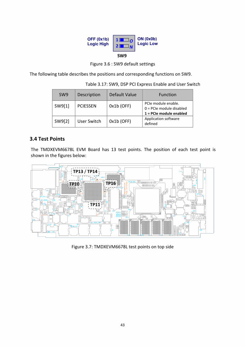
43
Figure 3.6 : SW9 default settings
The following table describes the positions and corresponding functions on SW9.
Table 3.17: SW9, DSP PCI Express Enable and User Switch
SW9 Description Default Value Function
SW9[1] PCIESSEN 0x1b (OFF) PCIe module enable.
0 = PCIe module disabled
1 = PCIe module enabled
SW9[2] User Switch 0x1b (OFF) Application software
defined
3.4 Test Points
The TMDXEVM6678L EVM Board has 13 test points. The position of each test point is
shown in the figures below:
Figure 3.7: TMDXEVM6678L test points on top side
OFF (0x1b) Logic High
O
N
SW9
2
1 ON (0x0b) Logic Low
TP13 / TP14
TP16 TP10
TP11
44
Figure 3.8: TMDXEVM6678L test points on the bottom side
Table 3.18 : TMDXEVM6678L EVM Board Test Points
Test Point Signal TP7 Reserved for MMC1 pin23
TP8 Reserved for MMC1 pin33
TP9 Reserved for MMC1 pin25
TP5 HyperLink_REFCLKOUTP
TP6 HyperLink_REFCLKOUTN
TP12 DSP_SYSCLKOUT
TP10 Reserved for U9 (FT2232) pin60 (PWREN#)
TP11 Reserved for U9 (FT2232) pin36 (SUSPEND#)
TP4 PHY1 (88E1111) 125MHz clock (default: disable)
TP13 Reserved for FPGA1 (XC3S200AN) pin A13 (+1.8V I/O).
TP14 Reserved for FPGA1 (XC3S200AN) pin A14 (+1.8V I/O).
TP15 Reserved for FPGA1 (XC3S200AN) pin M14 (+3.3V I/O).
TP16 Reserved for FPGA1 (XC3S200AN) pin L16 (+3.3V I/O).
3.5 System LEDs
The TMDXEVM6678L board has seven LEDs. Their positions on the board are indicated in
figure 3.7. The description of each LED is listed in table below:
Table 3.19 : TMDXEVM6678LTEEVM Board LEDs
LED# Color Description D1 Red Failure and Out of service status in AMC chassis
D2 Blue Hot Swap status in AMC chassis
SYSPG_D1 Green All Power rails are stable on AMC
FPGA_D1-
FPGA_D4 Blue Debug LEDs.
TP8 / TP9 / TP7
TP15
TP5
TP6
TP12
45
Figure 3.9: TMDXEVM6678L EVM Board LEDs
D1
D2
SYSPG_D1
FPGA_D1-D4
46
4. System Power Requirements
This chapter describes the power design of the TMDXEVM6678L board. It contains:
4.1 Power Requirements
4.2 Power Supply Distribution
4.3 Power Supply Boot Sequence
4.1 Power Requirements
Note that the power estimates stated in this section are maximum limits used in the design
of the EVM. They have margin added to allow the EVM to support early silicon samples that
normally have higher power consumption than eventual production units.
The maximum EVM power requirements are estimated to be:
• EVM FPGA – 0.65W;
• DSP Cooling Fans – 1.2W (+12Vdc/0.1A);
• Clock Generators & clock sources – 3.30W;
• DSP – 14.90W;[worse case]
� Core supplies: 13.0W;
� Peripheral supplies: 1.90W;
• DDR3 – 2.63W;
� 5 SDRAMs to support 64-bit with ECC of the DSP
• Misc – 0.33W;
• USB – 0.84W;
• SGMII PHY – 1.14W;
EVM board total: 31.2W;
The selected AC/DC 12V adapter should be rated for a minimum of 36 Watts.
47
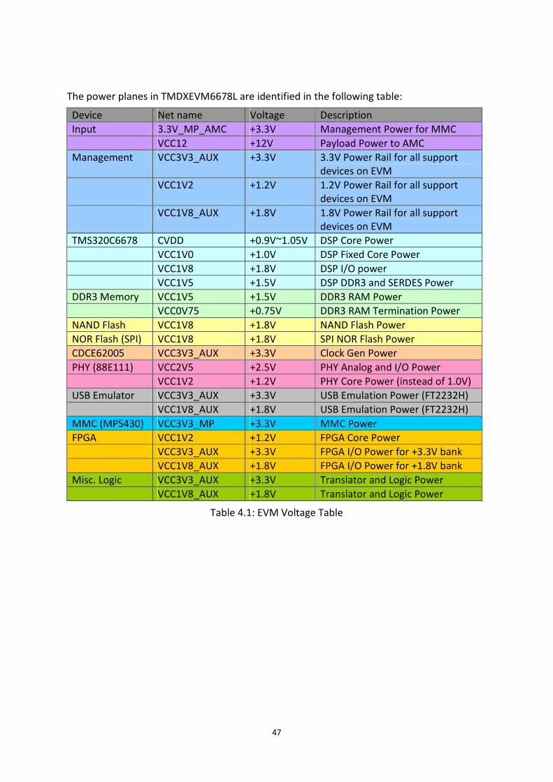
The power planes in TMDXEVM6678L are identified in the following table:
Device Net name Voltage Description
Input 3.3V_MP_AMC +3.3V Management Power for MMC
VCC12 +12V Payload Power to AMC
Management VCC3V3_AUX +3.3V 3.3V Power Rail for all support
devices on EVM
VCC1V2 +1.2V 1.2V Power Rail for all support
devices on EVM
VCC1V8_AUX +1.8V 1.8V Power Rail for all support
devices on EVM
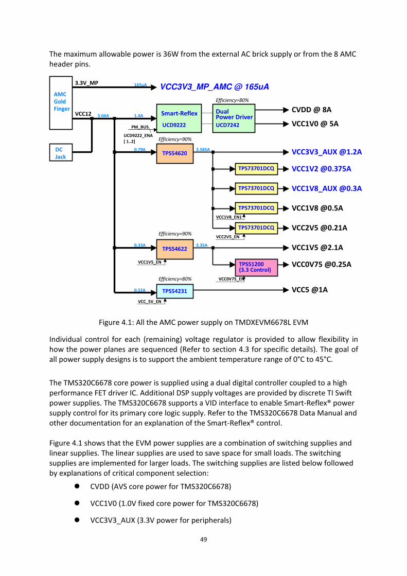
TMS320C6678 CVDD +0.9V~1.05V DSP Core Power
VCC1V0 +1.0V DSP Fixed Core Power
VCC1V8 +1.8V DSP I/O power
VCC1V5 +1.5V DSP DDR3 and SERDES Power
DDR3 Memory VCC1V5 +1.5V DDR3 RAM Power
VCC0V75 +0.75V DDR3 RAM Termination Power
NAND Flash VCC1V8 +1.8V NAND Flash Power
NOR Flash (SPI) VCC1V8 +1.8V SPI NOR Flash Power
CDCE62005 VCC3V3_AUX +3.3V Clock Gen Power
PHY (88E111) VCC2V5 +2.5V PHY Analog and I/O Power
VCC1V2 +1.2V PHY Core Power (instead of 1.0V)
USB Emulator VCC3V3_AUX +3.3V USB Emulation Power (FT2232H)
VCC1V8_AUX +1.8V USB Emulation Power (FT2232H)
MMC (MPS430) VCC3V3_MP +3.3V MMC Power
FPGA VCC1V2 +1.2V FPGA Core Power
VCC3V3_AUX +3.3V FPGA I/O Power for +3.3V bank
VCC1V8_AUX +1.8V FPGA I/O Power for +1.8V bank
Misc. Logic VCC3V3_AUX +3.3V Translator and Logic Power
VCC1V8_AUX +1.8V Translator and Logic Power
Table 4.1: EVM Voltage Table
48
The following table identifies the expected power requirements for each power plane of the
devices on the TMDXEVM6678L EVM.
TMS320C6678 V(V) I(A) Qty Pd (W)
CVDD 1.00 8.00 1 8.00
VCC1V0 1.00 5.00 1 5.00
VCC1V8 1.80 0.33 1 0.59
VCC1V5 1.50 0.85 1 1.28
14.87
DDR3 V(V) I(A) Qty Pd(W)
VCC1V5 1.50 0.30 5 2.25
VCC0V75 0.75 0.10 5 0.38 2.63
FPGA V(V) I(A) Qty Pd(W)
VCC3V3_AUX 3.30 0.03 1 0.10
VCC1V2 1.20 0.13 1 0.16
VCC1V8_AUX 1.80 0.20 1 0.36
0.62
XDS560V2 V(V) I(A) Qty Pd(W)
VCC5 5.00 1.00 1 5.00
VCC3V3_AUX 3.30 0.30 1 0.99 5.99
CDCE62005 V(V) I(A) Qty Pd(W)
VCC3V3_AUX 3.30 0.50 2 3.30 3.30
PHY (88E1111) V(V) I(A) Qty Pd(W)
VCC2V5_AUX 3.30 0.21 1 0.69
VCC1V2_AUX 1.80 0.25 1 0.45 1.14
FT2232 V(V) I(A) Qty Pd(W)
VCC3V3_AUX 3.30 0.21 1 0.69
VCC1V8_AUX 1.80 0.08 1 0.14 0.84
MMC (MSP430) V(V) I(A) Qty Pd(W)
VCC3V3_MP 3.30 0.02 1 0.07 0.07
Table 4.2: Each Current Requirements on each device of EVM board
4.2 The Power Supply Distribution
A high-level block diagram of the power supplies is shown in Figure 4.1. It is also shown on
the schematic.
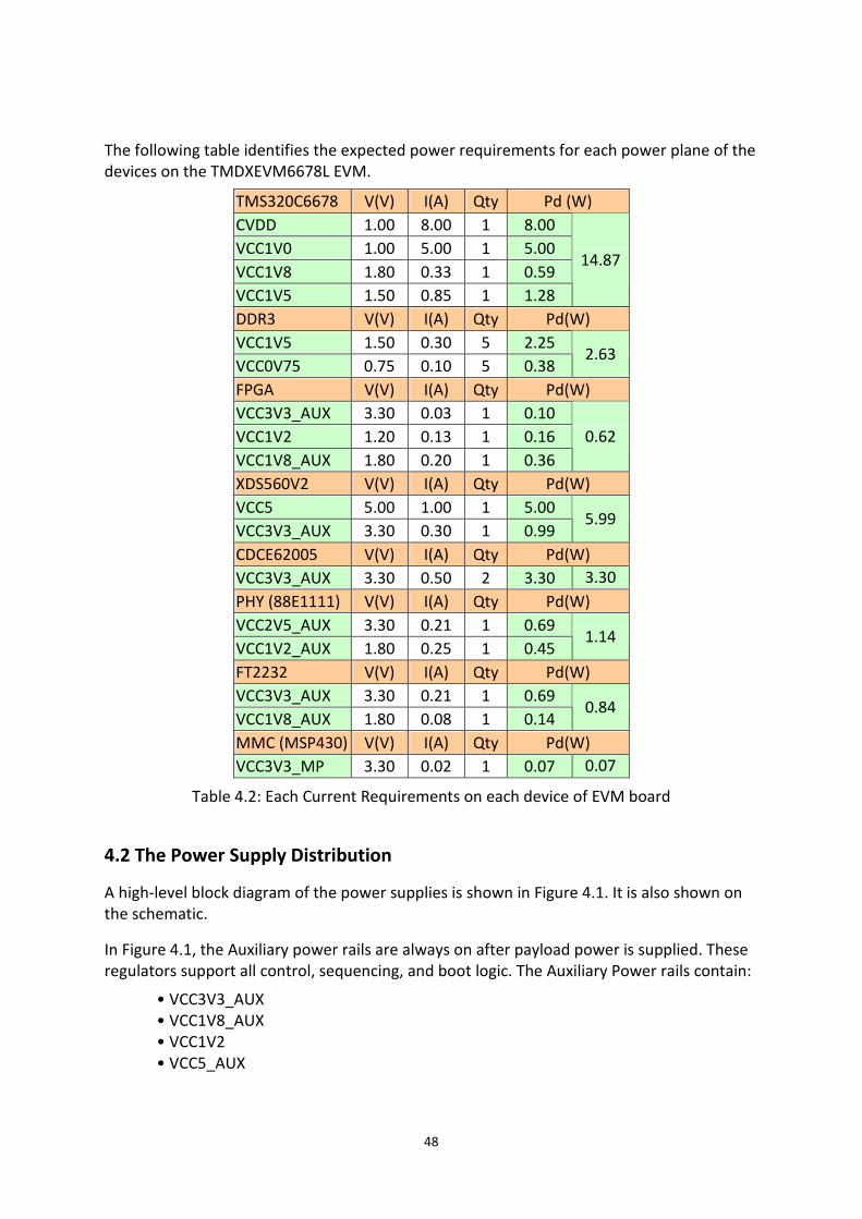
In Figure 4.1, the Auxiliary power rails are always on after payload power is supplied. These
regulators support all control, sequencing, and boot logic. The Auxiliary Power rails contain:
• VCC3V3_AUX
• VCC1V8_AUX
• VCC1V2
• VCC5_AUX
49
The maximum allowable power is 36W from the external AC brick supply or from the 8 AMC
header pins.
Figure 4.1: All the AMC power supply on TMDXEVM6678L EVM
Individual control for each (remaining) voltage regulator is provided to allow flexibility in
how the power planes are sequenced (Refer to section 4.3 for specific details). The goal of
all power supply designs is to support the ambient temperature range of 0°C to 45°C.
The TMS320C6678 core power is supplied using a dual digital controller coupled to a high
performance FET driver IC. Additional DSP supply voltages are provided by discrete TI Swift
power supplies. The TMS320C6678 supports a VID interface to enable Smart-Reflex® power
supply control for its primary core logic supply. Refer to the TMS320C6678 Data Manual and
other documentation for an explanation of the Smart-Reflex® control.
Figure 4.1 shows that the EVM power supplies are a combination of switching supplies and
linear supplies. The linear supplies are used to save space for small loads. The switching
supplies are implemented for larger loads. The switching supplies are listed below followed
by explanations of critical component selection:
� CVDD (AVS core power for TMS320C6678)
� VCC1V0 (1.0V fixed core power for TMS320C6678)
� VCC3V3_AUX (3.3V power for peripherals)
UCD9222_ENA
[ 1..2]
TPS51200 VCC0V75 @0.25A
VCC0V75_EN
Efficiency=90%
Efficiency=80%
2.35A 0.33A
0.79A
1.4A
2.585A
3.04A
165uA
0.52A
Efficiency=80%
TPS54231 VCC5 @1A
VCC_5V_EN
TPS73701DCQ VCC1V2 @0.375A
TPS73701DCQ VCC1V8_AUX @0.3A
VCC1V8 @0.5A
VCC12
UCD9222
Smart-Reflex
VCC2V5_EN
VCC1V5_EN
VCC2V5 @0.21A
VCC1V5 @2.1A
CVDD @ 8A
PM_BUS
TPS73701DCQ
VCC1V0 @ 5A
VCC3V3_MP_AMC @ 165uA 3.3V_MP
VCC3V3_AUX @1.2A TPS54620
VCC1V8_EN1 TPS73701DCQ
Power Driver Dual
UCD7242
TPS54622
Efficiency=90%
(3.3 Control)
AMC Gold Finger
DC Jack
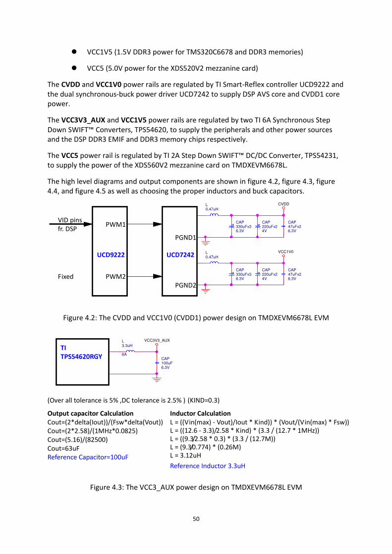
50
� VCC1V5 (1.5V DDR3 power for TMS320C6678 and DDR3 memories)
� VCC5 (5.0V power for the XDS520V2 mezzanine card)
The CVDD and VCC1V0 power rails are regulated by TI Smart-Reflex controller UCD9222 and
the dual synchronous-buck power driver UCD7242 to supply DSP AVS core and CVDD1 core
power.
The VCC3V3_AUX and VCC1V5 power rails are regulated by two TI 6A Synchronous Step
Down SWIFT™ Converters, TPS54620, to supply the peripherals and other power sources
and the DSP DDR3 EMIF and DDR3 memory chips respectively.
The VCC5 power rail is regulated by TI 2A Step Down SWIFT™ DC/DC Converter, TPS54231,
to supply the power of the XDS560V2 mezzanine card on TMDXEVM6678L.
The high level diagrams and output components are shown in figure 4.2, figure 4.3, figure
4.4, and figure 4.5 as well as choosing the proper inductors and buck capacitors.
Figure 4.2: The CVDD and VCC1V0 (CVDD1) power design on TMDXEVM6678L EVM
Figure 4.3: The VCC3_AUX power design on TMDXEVM6678L EVM
CAP 47uFx2 6.3V
L0.47uH
CAP 330uFx36.3V
CAP 220uFx24V
CVDD
CAP 47uFx2 6.3V
CAP 330uFx36.3V
L0.47uH
CAP 220uFx24V
VCC1V0 UCD7242UCD9222
PGND2
PGND1
PWM2
PWM1 fr. DSP
Fixed
VID pins
TPS54620RGY TI
CAP 100uF6.3V
L 3.3uH 6A
VCC3V3_AUX
(KIND=0.3)
Cout=63uF Cout=(5.16)/(82500)
Cout=(2*2.58)/(1MHz*0.0825)
Cout=(2*delta(Iout))/(Fsw*delta(Vout))
(Over all tolerance is 5% ,DC tolerance is 2.5% )
Inductor Calculation
Reference Inductor 3.3uH
Output capacitor Calculation L = ((Vin(max) - Vout)/Iout * Kind)) * (Vout/(Vin(max) * Fsw)) L = ((12.6 - 3.3)/2.58 * Kind) * (3.3 / (12.7 * 1MHz)) L = ((9.3/2.58 * 0.3) * (3.3 / (12.7M)) L = (9.3/0.774) * (0.26M) L = 3.12uH Reference Capacitor=100uF
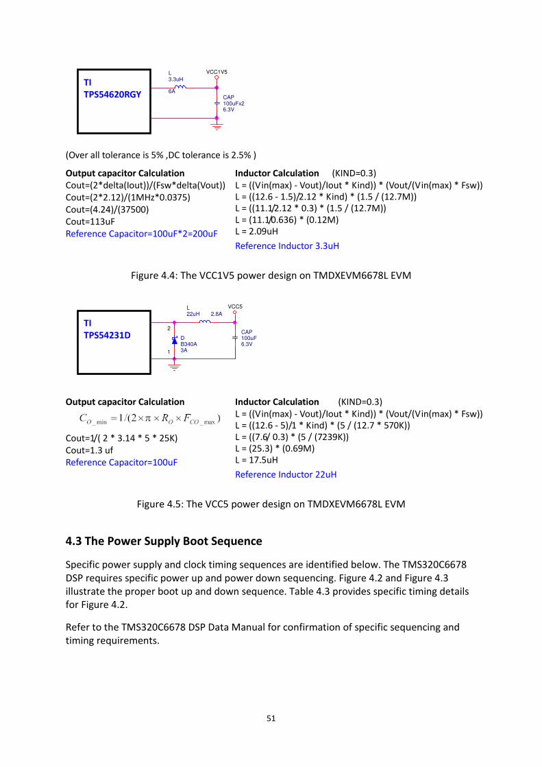
51
Figure 4.4: The VCC1V5 power design on TMDXEVM6678L EVM
Figure 4.5: The VCC5 power design on TMDXEVM6678L EVM
4.3 The Power Supply Boot Sequence
Specific power supply and clock timing sequences are identified below. The TMS320C6678
DSP requires specific power up and power down sequencing. Figure 4.2 and Figure 4.3
illustrate the proper boot up and down sequence. Table 4.3 provides specific timing details
for Figure 4.2.
Refer to the TMS320C6678 DSP Data Manual for confirmation of specific sequencing and
timing requirements.
TPS54620RGY CAP 100uFx26.3V
TI L 3.3uH 6A
VCC1V5
(KIND=0.3)
(Over all tolerance is 5% ,DC tolerance is 2.5% )
Output capacitor Calculation
Cout=113uF
Cout=(4.24)/(37500)
Cout=(2*2.12)/(1MHz*0.0375) Cout=(2*delta(Iout))/(Fsw*delta(Vout))
Inductor Calculation
Reference Inductor 3.3uH
L = ((Vin(max) - Vout)/Iout * Kind)) * (Vout/(Vin(max) * Fsw)) L = ((12.6 - 1.5)/2.12 * Kind) * (1.5 / (12.7M)) L = ((11.1/2.12 * 0.3) * (1.5 / (12.7M)) L = (11.1/0.636) * (0.12M) L = 2.09uH Reference Capacitor=100uF*2=200uF
D B340A 3A 1
2
L 22uH 2.8A
CAP 100uF 6.3V
VCC5
TI TPS54231D
L = ((Vin(max) - Vout)/Iout * Kind)) * (Vout/(Vin(max) * Fsw)) L = ((12.6 - 5)/1 * Kind) * (5 / (12.7 * 570K)) L = ((7.6/ 0.3) * (5 / (7239K)) L = (25.3) * (0.69M) L = 17.5uH
Inductor Calculation
Reference Inductor 22uH
(KIND=0.3)
Reference Capacitor=100uF Cout=1.3 uf
Cout=1/( 2 * 3.14 * 5 * 25K)
Output capacitor Calculation
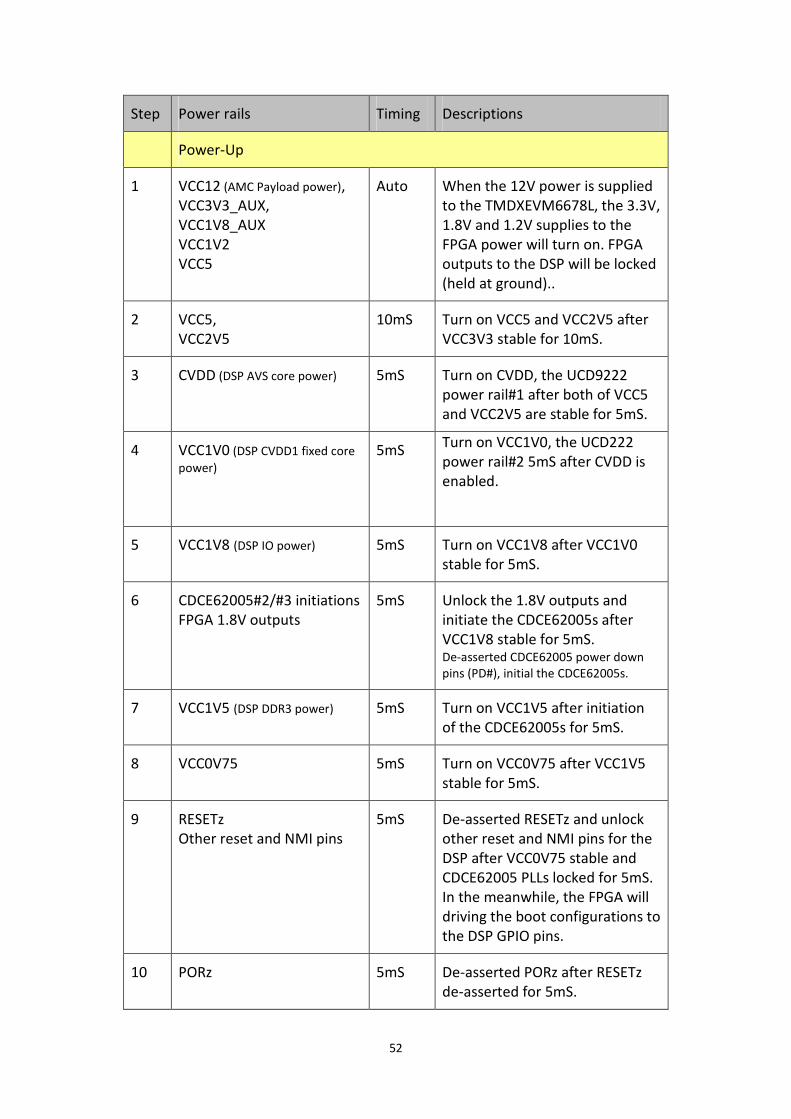
52
Step Power rails Timing Descriptions
Power-Up
1 VCC12 (AMC Payload power),
VCC3V3_AUX,
VCC1V8_AUX
VCC1V2
VCC5
Auto When the 12V power is supplied
to the TMDXEVM6678L, the 3.3V,
1.8V and 1.2V supplies to the
FPGA power will turn on. FPGA
outputs to the DSP will be locked
(held at ground)..
2 VCC5,
VCC2V5
10mS Turn on VCC5 and VCC2V5 after
VCC3V3 stable for 10mS.
3 CVDD (DSP AVS core power) 5mS Turn on CVDD, the UCD9222
power rail#1 after both of VCC5
and VCC2V5 are stable for 5mS.
4 VCC1V0 (DSP CVDD1 fixed core
power) 5mS
Turn on VCC1V0, the UCD222
power rail#2 5mS after CVDD is
enabled.
5 VCC1V8 (DSP IO power) 5mS Turn on VCC1V8 after VCC1V0
stable for 5mS.
6 CDCE62005#2/#3 initiations
FPGA 1.8V outputs
5mS Unlock the 1.8V outputs and
initiate the CDCE62005s after
VCC1V8 stable for 5mS. De-asserted CDCE62005 power down
pins (PD#), initial the CDCE62005s.
7 VCC1V5 (DSP DDR3 power) 5mS Turn on VCC1V5 after initiation
of the CDCE62005s for 5mS.
8 VCC0V75 5mS Turn on VCC0V75 after VCC1V5
stable for 5mS.
9 RESETz
Other reset and NMI pins
5mS De-asserted RESETz and unlock
other reset and NMI pins for the
DSP after VCC0V75 stable and
CDCE62005 PLLs locked for 5mS.
In the meanwhile, the FPGA will
driving the boot configurations to
the DSP GPIO pins.
10 PORz 5mS De-asserted PORz after RESETz
de-asserted for 5mS.
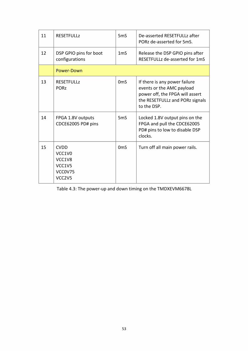
53
11 RESETFULLz 5mS De-asserted RESETFULLz after
PORz de-asserted for 5mS.
12 DSP GPIO pins for boot
configurations
1mS Release the DSP GPIO pins after
RESETFULLz de-asserted for 1mS
Power-Down
13 RESETFULLz
PORz
0mS If there is any power failure
events or the AMC payload
power off, the FPGA will assert
the RESETFULLz and PORz signals
to the DSP.
14 FPGA 1.8V outputs
CDCE62005 PD# pins
5mS Locked 1.8V output pins on the
FPGA and pull the CDCE62005
PD# pins to low to disable DSP
clocks.
15 CVDD
VCC1V0
VCC1V8
VCC1V5
VCC0V75
VCC2V5
0mS Turn off all main power rails.
Table 4.3: The power-up and down timing on the TMDXEVM6678L
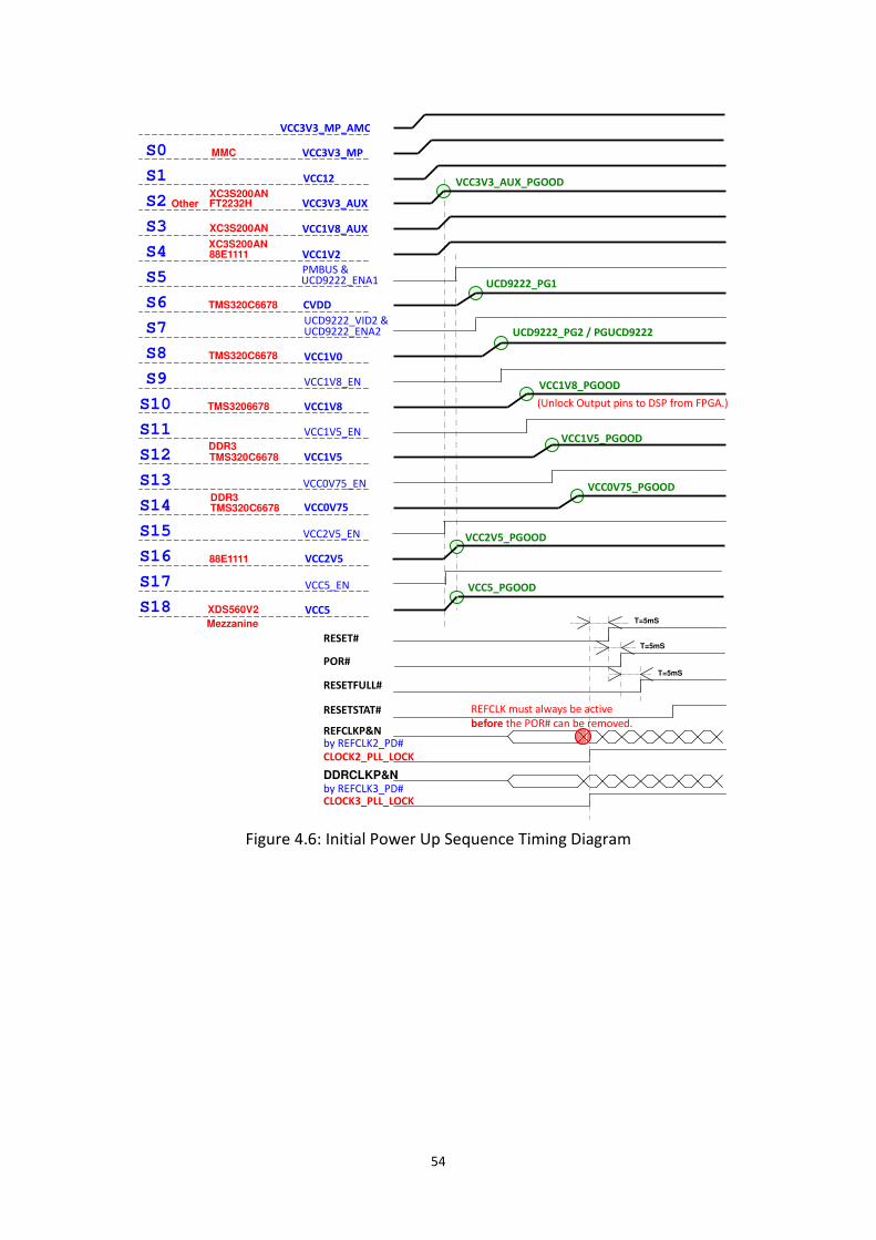
54
Figure 4.6: Initial Power Up Sequence Timing Diagram
RESETSTAT#
REFCLKP&N
DDRCLKP&N
RESET# T=5mS
RESETFULL#
VCC3V3_MP_AMC
S6
S0
S3
S4
S5
S7
S8
S9
S10
88E1111
VCC0V75_PGOOD
VCC1V5_PGOOD
VCC1V8_PGOOD
UCD9222_PG2 / PGUCD9222
UCD9222_PG1
VCC2V5_PGOOD
VCC3V3_AUX_PGOOD
VCC5_PGOOD
PMBUS &
UCD9222_ENA2
VCC1V8_EN
VCC1V5_EN
VCC0V75_EN
VCC2V5_EN
FT2232H Other
S11
S13
S12
S14
S15
S16 88E1111
POR#
T=5mS
VCC3V3_AUX
TMS320C6678 CVDD
VCC3V3_MP
VCC1V8_AUX XC3S200AN
S1 VCC12
XC3S200AN
VCC2V5
VCC1V8
VCC1V0 TMS320C6678
TMS3206678
DDR3
DDR3
MMC
TMS320C6678
TMS320C6678
VCC5_EN S17
S18 XDS560V2 VCC5
VCC1V2 XC3S200AN
S2
VCC0V75
UCD9222_ENA1
VCC1V5
UCD9222_VID2 &
by REFCLK3_PD#
by REFCLK2_PD#
CLOCK2_PLL_LOCK
CLOCK3_PLL_LOCK
(Unlock Output pins to DSP from FPGA.)
REFCLK must always be active
before the POR# can be removed.
Mezzanine
T=5mS
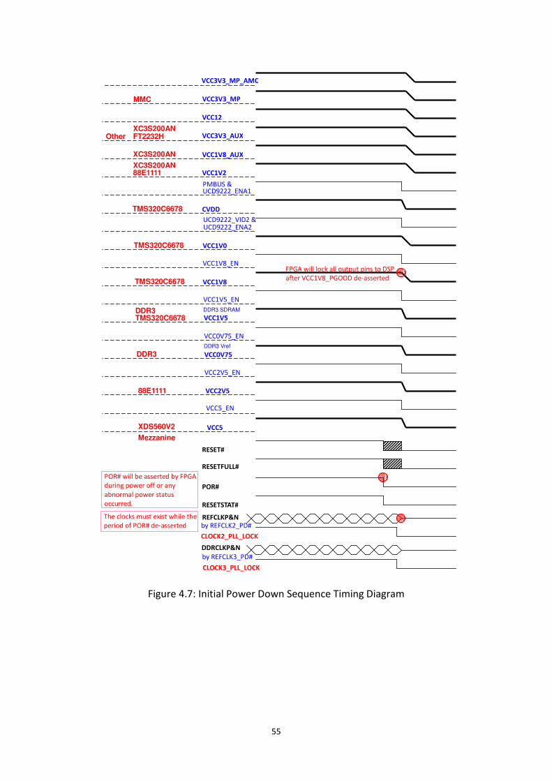
55
Figure 4.7: Initial Power Down Sequence Timing Diagram
PMBUS &
UCD9222_ENA2
VCC1V8_EN
VCC1V5_EN
VCC0V75_EN
VCC2V5_EN
Other FT2232H
88E1111
POR#
VCC3V3_AUX
TMS320C6678 CVDD
VCC3V3_MP
XC3S200AN VCC1V8_AUX
VCC12
XC3S200AN
VCC2V5
VCC1V8
DDR3 SDRAM
VCC1V0 TMS320C6678
TMS320C6678
DDR3 Vref
DDR3
DDR3
MMC
TMS320C6678
VCC5_EN
XDS560V2 VCC5
VCC1V2 XC3S200AN
VCC0V75
UCD9222_VID2 &
VCC1V5
UCD9222_ENA1
by REFCLK2_PD#
by REFCLK3_PD#
CLOCK3_PLL_LOCK
CLOCK2_PLL_LOCK
RESETSTAT#
REFCLKP&N
DDRCLKP&N
RESET#
RESETFULL#
VCC3V3_MP_AMC
88E1111
FPGA will lock all output pins to DSP
after VCC1V8_PGOOD de-asserted
POR# will be asserted by FPGA
during power off or any
abnormal power status
occurred.
The clocks must exist while the
period of POR# de-asserted
Mezzanine
56
5. TMDXEVM6678L FPGA FUNCTIONAL DESCRIPTION
This chapter contains,
5.1 FPGA overview
5.2 FPGA signals description
5.3 Sequence of operation
5.4 Reset definition
5.5 SPI protocol
5.6 CDCE62005 Programming Descriptions
5.7 FPGA Configuration Registers
5.1 FPGA overview
The FPGA (Xilinx XC3S200AN) controls the EVM power sequencing, reset mechanism, DSP
boot mode configuration and clock initialization. The FPGA also provides the transformation
of TDM Frame Synchronization signal and Reference Clock between the AMC connector and
the DSP.
The FPGA also supports 4 user LEDs and 1 user switch through control registers. All the FPGA
registers are accessible by the TMS320C6678 DSP.
The key features of the TMDXEVM6678L EVM FPGA are:
� TMDXEVM6678L EVM Power Sequence Control
� TMDXEVM6678L EVM Reset Mechanism Control
� TMDXEVM6678L EVM Clock Generator Initialization and Control
� TMS320C6678 DSP SPI Interface for Accessing the FPGA Configurable Registers
� Provides Shadow Registers for TMS320C6678 DSP to Access the Clock Generator
Configurations Registers
� Provides Shadow Registers for TMS320C6678 DSP to Access the UCD9222
Devices via the PM Bus (RFU)
� Provides TMS320C6678 DSP Boot Mode Configuration switch settings to DSP
� MMC Reset Events Initiation Interface
� Provides the transformation of TDM Frame Synchronization and Reference Clock
between AMC and DSP
57
� Provide Ethernet PHY Interrupt(RFU) and Reset Control Interface
� Provides support for Reset Buttons, User Switches and Debug LEDs
5.2 FPGA signals description
This section provides a detailed description of each signal. The signals are arranged in
functional groups according to their associated interface. Throughout this manual, a ‘#’ or ‘Z’
will be used at the end of a signal name to indicate that the active or asserted state occurs
when the signal is at a low voltage level.
The following notations are used to describe the signal and type.
I Input pin
O Output pin
I/O Bi-directional pin
Differential Differential Pair pins
PU Internal Pull-Up
.
Table 5.1 : TMDXEVM6678L EVM FPGA Pin Description
Pin Name IO Type Description
MMC Control :
MMC_DETECT# I
PU
MMC Detection on the insertion to an AMC
Chassis : This signal is an insertion indication
from the MMC. The MMC will drive logic low
state when the EVM module is inserted into an
AMC chassis.
MMC_RESETSTAT# O RESETSTAT# state to MMC : The FPGA will
drive the same status of the DSP RESETSTAT# to
the MMC via this signal.
MMC_POR_IN_AMC# I
PU
MMC POR Request : This signal is used by the
MMC to request a power-on reset sequence to
DSP. A logic Low to High transition on this
signal will complete the FPGA Full Reset
sequence with a specified delay time.
MMC_WR_AMC# I
PU
MMC WARM Request : This signal is used by
the MMC to initiate a warm reset request. A
logic Low to High transition on this signal will
complete the FPGA warm reset sequence with
a specified delay time.
58
Pin Name IO Type Description
MMC_BOOTCOMPLET
E
O BOOTCOMPLETE state to MMC : The FPGA will
drive the same status of the DSP
BOOTCOMPLETE to the MMC via this signal.
Power Sequences Control :
VCC5_PGOOD I 5V Voltage Power Good Indication : This signal
indicates the 5V power is valid.
VCC2P5_PGOOD I 2.5V Voltage Power Good Indication : This
signal indicates the 2.5V power is valid.
VCC3_AUX_PGOOD I 3.3V Auxiliary Voltage Power Good
Indication : This signal indicates the 3.3V
auxiliary power is valid.
VCC0P75_PGOOD I 0.75V Voltage Power Good Indication : This
signal indicates the 0.75V power is valid.
VCC1P5_PGOOD I 1.5V Voltage Power Good Indication : This
signal indicates the 1.5V power is valid.
VCC1P8_PGOOD I 1.8V Voltage Power Good Indication : This
signal indicates the 1.8V power is valid.
SYS_PGOOD O System Power Good Indication : This signal is
indicated by the FPGA to the system when all
the power supplies are valid.
VCC1P8_EN1 O 1.8V Voltage Power Supply Enable :
VCC1P8_EN1 is for 1.8V power plane control.
VCC0P75_EN O 0.75V Voltage Power Supply Enable :
VCC0P75_EN is for 0.75V power plane control.
VCC2P5_EN O 2.5V Voltage Power Supply Enable :
VCC2P5_EN is for 2.5V power plane control.
VCC_5V_EN O 5V Voltage Power Supply Enable : VCC_5V_EN
is for 5V power plane control.
CLOCK Configurations :
CLOCK[2:3]_SSPCS1 O SPI Chip Select Enable : This signal is
connected to the TI CDCE62005 CLOCK
Generators SPI_LE pin. The falling edge of the
SSPCS1 initiates a transfer. If SSPCS1 is high, no
data transfer can take place.
CLOCK[2:3]_SSPCK O SPI Serial Clock : This signal is connected to the
TI CDCE62005 CLOCK Generators SPI_CLK pin.
The FPGA SPI bus clocks data in and out on the
rising edge of SSPCK. Data transitions therefore
occur on the falling edge of the clock.
CLOCK[2:3]_SSPSI O SPI Serial Data MOSI : This signal is connected
to the TI CDCE62005 CLOCK Generators MOSI
pin. This signal is used for serial data
transfers from the master (FPGA) output to the
slave (CDCE62005) input.
59
Pin Name IO Type Description
CLOCK[2:3]_SSPSO I
PU
SPI Serial Data MISO : This signal is connected
to the TI CDCE62005 CLOCK Generators MISO
pin. This signal is used for the serial data
transfers from the slave (CDCE62005) output to
the master (FPGA) input.
REFCLK[2:3]_PD# O TI CDCE62005 CLOCK Generator Power Down :
The power down pins each place the respective
CDCE62005 into the power down state forcing
the differential clock output into the
high-impedance state.
UCD9222 Interface :
UCD9222_PG1 I UCD9222 Power Good Indication for CVDD
DSP Core Power : This signal indicates the
CVDD DSP core power is valid.
UCD9222_ENA1 O UCD9222 Enable for CVDD DSP Core Power :
UCD9222_ENA1 is for CVDD DSP core power
plane control.
UCD9222_PG2 I UCD9222 Power Good Indication for VCC1V0
DSP Core Power : This signal indicates the
VCC1V0 DSP core power is valid.
UCD9222_ENA2 O UCD9222 Enable for VCC1V0 DSP Core Power :
UCD9222_ENA2 is for VCC1V0 DSP core power
plane control.
PGUCD9222 I UCD9222 Power Good Indication : This signal
indicates both the CVDD DSP and VCC1V0 DSP
core power supplies are valid.
UCD9222_RST# O UCD9222 Reset : An active low signal will reset
the UCD9222 device.
PM BUS : (RFU)
PMBUS_CLK O PM Bus Clock : The FPGA provides the clock
source on the PM bus.
PMBUS_DAT I/O PM Bus Data : A PM Bus slave device can
receive data provided by the master (FPGA), or
it can also provide data to the master (FPGA)
via this signal line.
PMBUS_ALT I PM Bus Alert : The PM Bus device may notify
the host (FPGA) via this signal if a fault or
warning is detected.
PMBUS_CTL I
PU
PM Bus Control : This signal is used to turn the
device on and off in conjunction with
UCD9222_ENA1 / UCD9222_ENA2 pins.
PHY Interface :
PHY_INT# I Interrupt Request from 88E111 PHY (RFU)
60
Pin Name IO Type Description
PHY_RST# O Reset to 88E1111 PHY : This signal is used to
reset the 88E1111 PHY device. The PHY_RST#
will be asserted during the active DSP_PORZ or
DSP_RESETFULLZ period. The PHY_RST# logic
also can be configured by the DSP accessed
register.
DSP SPI :
DSP_SSPCS1 I DSP SPI Chip Select 1 : This signal is connected
to the TMS320C6678 DSP SPISCS1 pin. The
falling edge of the SSPCS1 from the DSP will
initiate a transfer. If SSPCS1 is high, no data
transfer can take place.
DSP_SSPCK I DSP SPI Serial Clock : This signal is connected
to the TMS320C6678 DSP SPICLK pin. The FPGA
SPI bus clocks data in on the falling edge of
SSPCK. Data transitions therefore occur on the
rising edge of the clock.
DSP_SSPMISO O DSP SPI Serial Data MISO : This signal is
connected to the TMS320C6678 DSP SPIDIN
pin. This signal is used for serial data
transfers from the slave (FPGA) output to the
master (DSP) input in the DSP_SSPCS1 asserted
period.
DSP_SSPMOSI I DSP SPI Serial Data MOSI : This signal is
connected to the DSP SPIDOUT pin. This signal
is used for serial data transfers from the master
(DSP) output to the slave (FPGA) input.
RESET Buttons and Requests :
FULL_RESET I Full Reset Button Input : This button input is
used to initiate a Full Reset event.
WARM_RESET I Warm Reset Button Input : This button input is
used to initiate a Warm Reset event.
COLD_RESET
(RFU)
I Cold Reset Button Input :
Reserved for Future Use (RFU).
FPGA_JTAG_RST#
(RFU)
I FPGA JTAG Reset Input :
Reserved for Future Use (RFU).
TRGRSTZ I Reset Request from the DSP Emulator
Header : A warm Reset sequence will be
initiated if an active TRGRSTZ event is
recognized by the FPGA.
DSP Boot & Device configurations :
BM_GPIO[0 : 15] I DSP Boot Mode Strap Configurations : These
switch inputs are used to drive the DSP boot
mode configuration during the EVM power up
period.
61
Pin Name IO Type Description
DSP_GPIO[0 : 15] I/O DSP GPIO : In normal operation mode, these
signals are not driven by the FPGA so that the
DSP can use them as GPIO pins. During the
EVM power-on or during the RESETFULLz
asserted period, the FPGA will output the
BM_GPIO switch values to the DSP on these
pins so the DSP can latch the boot mode
configuration.
DSP RESET & Interrupts Control :
DSP_CORESEL[0:3] O DSP Core Selection Bit:
The default value is 0000b and Register bits
define the state of these pins.
DSP_PACLKSEL O DSP PACLKSEL : This pin is used for the DSP
PASS clock selection setting. The logic of this
signal is derived from the BM_GPIO[13:11]
state or configured by the FPGA registors.
DSP_LRESETNMIENZ O Latch Enable for DSP Local Reset and NMI
inputs :The default value is 1b and a register
bit defines the state of this pin.
DSP_NMIZ O DSP NMI.
The default value is 1b and unlocked a register
bit defines the state of this pin.
DSP_LRESETZ O DSP Local Reset.
The default value is 1b and a register bit
defines the state of this pin.
DSP_HOUT I DSP HOUT
DSP_BOOTCOMPLETE I DSP Boot Complete Indication
DSP_SYSCLKOUT I DSP System Clock Output
DSP_PORZ O DSP Power-On Reset
DSP_RESETFULLZ O DSP Full Reset.
DSP_RESETZ O DSP Reset
FPGA Storage (RFU):
FPGA_SPI_CS# O FPGA SPI Chip Select : (RFU)
FPGA_SPI_SI O FPGA SPI Serial Data MOSI : (RFU)
FPGA_SPI_SCK O FPGA SPI Clock Output : (RFU)
FPGA_SPI_SO I FPGA SPI Serial Data MISO : (RFU)
DSP TDM CLK :
DSP_TSIP0_FS[A:B]0 O DSP TSIP0_FS[A:B]0 : The single-ended clock
(DSP_TSIP0_FSA0 and DSP_TSIP0_FSB0)
outputs are derived from the differential TDM
Frame Synchronization (TDM_CLKC) input.
62
Pin Name IO Type Description
DSP_TSIP1_FS[A:B]1 O DSP TSIP1_FS[A:B]1 : The single-ended clock
(DSP_TSIP1_FSA1 and DSP_TSIP1_FSB1)
outputs are derived from the differential TDM
Frame Synchronization (TDM_CLKC) input.
DSP_TSIP0_CLK[A:B]0 O DSP TSIP0_CLK[A:B]0 : The single-ended clock
(DSP_TSIP0_CLKA0 and DSP_TSIP0_CLKB0)
outputs are derived from the differential TDM
clock (TDM_CLKA) input.
DSP_TSIP1_CLK[A:B]1 O DSP TSIP1_CLK[A:B]1 : The single-ended clock
(DSP_TSIP1_CLKA1 and DSP_TSIP1_CLKB1)
outputs are derived from the differential TDM
clock (TDM_CLKA) input.
TDM_CLKA[p/n] I, Diff TDM_CLKA Different Clock Input Pairs
The reference clock referring to the TSIP0/1
CLKs of the DSP.
TDM_CLKB[p/n]
(RFU)
I, Diff TDM_CLKB Different Clock Input Pairs
Reserved for future use (RFU).
TDM_CLKC[p/n] I, Diff TDM_CLKC Different Clock Input Pairs
The frame synchronization signal referring to
the TSIP0/1 FSs of the DSP.
TDM_CLKD[p/n]
(RFU)
I, Diff TDM_CLKD Different Clock Input Pairs
Reserved for future use (RFU)
DEBUG LED:
DEBUG_LED[1:4] O Debug LED : The LEDs are used for debugging
purposes only. It can be configured by the
registers in the FPGA.
Miscellaneous :
MAIN_48MHZ_CLK_R I FPGA Main Clock Source : A 48 MHz clock is
used as the FPGA main clock source.
DSP_TIMI0 O DSP Timer 0 Clock : The FPGA provides a
24MHz clock to the DSP timer 0 input. During
the EVM Power-on or RESETFULLZ asserted
period, the FPGA will drive the PCIESSEN
switch state to DSP for latching.
DSP_VCL_1 (RFU) I DSP Smart Reflex I2C Clock
DSP_VD_1 (RFU) I/O DSP Smart Reflex I2C Clock
PCA9306_EN O PCA9306 Enable : This signal is used to enable
the DSP Smart Reflex I2C buffer function.
NAND_WP# O NAND Flash Write Protect : This signal is used
to control the NAND flash write-protect
function.
NOR_WP# O NOR Flash Write Protect : This signal is used to
control the NOR flash write-protect function.
EEPROM_WP O EEPROM Write Protect : This signal is used to
control the EEPROM write-protect function.
63
Pin Name IO Type Description
PCIESSEN I PCIE Subsystem Enable : This is used for the
PCIESSEN switch input.
USER_DEFINE I User Defined Switch : This is reserved for the
user defined switch input.
XDS560_IL O XDS560 IL : XDS560 IL control signal
FPGA JTAG TAP Control Port:
JTAG_FPGA_TCK I FPGA JTAG Clock Input
JTAG_FPGA_TDI I FPGA JTAG Data Input
JTAG_FPGA_TDO O FPGA JTAG Data Output
JTAG_FPGA_TMS I FPGA JTAG Mode Select Input
JTAG_FPGA_RST# I FPGA JTAG Reset (RFU)
5.3 Sequence of operation
This section describes the FPGA sequence of operation on the EVM. It contains:
5.3.1 Power-On Sequence
5.3.2 Power Off Sequence
5.3.3 Boot Configuration Timing
5.3.4 Boot Configuration Forced in I2C Boot
5.3.1 Power-On Sequence
The following section provides details of the FPGA Power-On sequence of operation.
1. After the EVM 3.3V auxiliary voltage (VCC3V3_AUX_PGOOD) is valid and stable, and
the FPGA design code is loaded, the FPGA is ready for the Power-On sequence of
operation.
2. The FPGA starts to execute the Power-On sequence. Wait for 10 ms, the FPGA enable
the 2.5V power.
3. Once the 2.5V voltages (VCC5_PGOOD and VCC2V5_PGOOD) is valid, wait for 5 ms,
the FPGA asserts the UCD9222_ENA1 to enable the CVDD DSP core power.
4. After the UCD9222_ENA1 enabled for 5 ms, the FPGA asserts the UCD9222_ENA2 to
enable the VCC1V0 DSP core power.
5. After both the UCD9222_PG1, UCD9222_PG2 and PGUCD9222 are all valid, wait for 5
ms, the FPGA enables the 1.8V power.
6. After the 1.8V voltage is valid (VCC1V8_PGOOD asserted), wait for 5 ms and then:
• Unlock the 1.8V outputs on the FPGA,
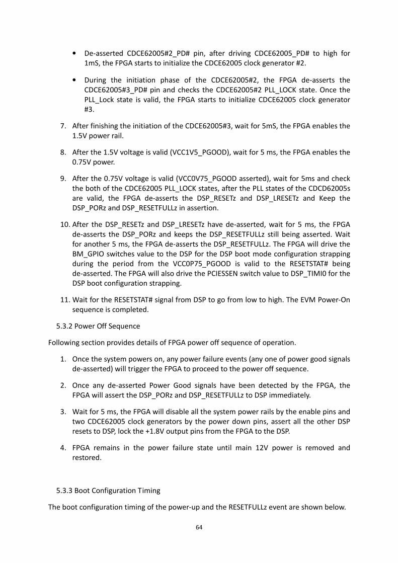
64
• De-asserted CDCE62005#2_PD# pin, after driving CDCE62005_PD# to high for
1mS, the FPGA starts to initialize the CDCE62005 clock generator #2.
• During the initiation phase of the CDCE62005#2, the FPGA de-asserts the
CDCE62005#3_PD# pin and checks the CDCE62005#2 PLL_LOCK state. Once the
PLL_Lock state is valid, the FPGA starts to initialize CDCE62005 clock generator
#3.
7. After finishing the initiation of the CDCE62005#3, wait for 5mS, the FPGA enables the
1.5V power rail.
8. After the 1.5V voltage is valid (VCC1V5_PGOOD), wait for 5 ms, the FPGA enables the
0.75V power.
9. After the 0.75V voltage is valid (VCC0V75_PGOOD asserted), wait for 5ms and check
the both of the CDCE62005 PLL_LOCK states, after the PLL states of the CDCD62005s
are valid, the FPGA de-asserts the DSP_RESETz and DSP_LRESETz and Keep the
DSP_PORz and DSP_RESETFULLz in assertion.
10. After the DSP_RESETz and DSP_LRESETz have de-asserted, wait for 5 ms, the FPGA
de-asserts the DSP_PORz and keeps the DSP_RESETFULLz still being asserted. Wait
for another 5 ms, the FPGA de-asserts the DSP_RESETFULLz. The FPGA will drive the
BM_GPIO switches value to the DSP for the DSP boot mode configuration strapping
during the period from the VCC0P75_PGOOD is valid to the RESETSTAT# being
de-asserted. The FPGA will also drive the PCIESSEN switch value to DSP_TIMI0 for the
DSP boot configuration strapping.
11. Wait for the RESETSTAT# signal from DSP to go from low to high. The EVM Power-On
sequence is completed.
5.3.2 Power Off Sequence
Following section provides details of FPGA power off sequence of operation.
1. Once the system powers on, any power failure events (any one of power good signals
de-asserted) will trigger the FPGA to proceed to the power off sequence.
2. Once any de-asserted Power Good signals have been detected by the FPGA, the
FPGA will assert the DSP_PORz and DSP_RESETFULLz to DSP immediately.
3. Wait for 5 ms, the FPGA will disable all the system power rails by the enable pins and
two CDCE62005 clock generators by the power down pins, assert all the other DSP
resets to DSP, lock the +1.8V output pins from the FPGA to the DSP.
4. FPGA remains in the power failure state until main 12V power is removed and
restored.
5.3.3 Boot Configuration Timing
The boot configuration timing of the power-up and the RESETFULLz event are shown below.
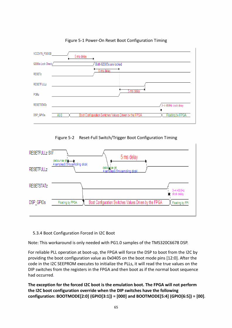
65
Figure 5-1 Power-On Reset Boot Configuration Timing
Figure 5-2 Reset-Full Switch/Trigger Boot Configuration Timing
5.3.4 Boot Configuration Forced in I2C Boot
Note: This workaround is only needed with PG1.0 samples of the TMS320C6678 DSP.
For reliable PLL operation at boot-up, the FPGA will force the DSP to boot from the I2C by
providing the boot configuration value as 0x0405 on the boot mode pins [12:0]. After the
code in the I2C SEEPROM executes to initialize the PLLs, it will read the true values on the
DIP switches from the registers in the FPGA and then boot as if the normal boot sequence
had occurred.
The exception for the forced I2C boot is the emulation boot. The FPGA will not perform
the I2C boot configuration override when the DIP switches have the following
configuration: BOOTMODE[2:0] (GPIO[3:1]) = [000] and BOOTMODE[5:4] (GPIO[6:5]) = [00].

66
Therefore, the additional logic of the FPGA will allow the emulation boot to latch directly
from the DIP switches.
5.4 Reset definition
5.4.1 Reset Behavior
� Power-On : The Power-On behavior includes initiating and sequencing the power
sources, clock sources and then DSP startup. Please refer to the section 5.5.1 for
detailed sequence and operations.
� Full Reset : The RESETFULLz is asserted low to the DSP. This causes RESETSTAT# to
go low which triggers the boot configuration to be driven from the FPGA. Reset to
the Marvell PHY is also asserted. POR# and RESET# to the DSP remain high. The
power supplies and clocks operate without interruption. Please refer to the section
5.5.3 for detailed timing diagrams.
� Warm Reset : The RESETz is asserted low to the DSP. The PORz and RESETFULLz to
the DSP remain high. The power supplies and clocks operate without interruption.
5.4.2 Reset Switches and Triggers
� FULL_RESET (RST_FULL1) – a logic low state with a low to high transition will trigger a
Full Reset behavior event.
When the push button switch RST_FULL1 is pressed, FPGA on EVM will assert DSP’s
RESETFULL# input to issue a total reset of the DSP, everything on the DSP will be reset to
its default state in response to this event, boot configurations will be latched and the
ROM boot process will be initiated.
This is equivalent to a power cycle of the board but POR and will have following effects:
* Reset DSP
* Reset Gigabit Ethernet PHY
* Reload boot parameters.
* Protect the conents in the I2C EEPROM, NAND flash and SPI NOR flash.
� WARM_RESET (RST_WARM1) – a logic low state with a low to high transition will
trigger a warm reset behavior event.
When the push button Switch RST_WARM1 is pressed, FPGA will assert a DSP RESET#
input, which will reset the DSP. Software can program this to be either hard or soft. Hard
reset is the default which resets almost everything. Soft Reset will behave like Hard Reset
except that PCIe MMRs, EMIF16 MMRs, DDR3 EMIF MMRs, and External Memory
contents are retained.
Boot configurations are not latched by Warm Reset. Also, Warm Reset will not reset
67
blocks supporting Reset Isolation when they are appropriately configured previously by
application software. Warm Reset must be used to wake from low-power sleep and
hibernation modes.
In the case of a Soft Reset, the clock logic or the power control logic of the peripherals are
not affected, and, therefore, the enabled/disabled state of the peripherals is not affected.
The following external memory contents are maintained
During a Soft Reset:
• DDR3 MMRs: The DDR3 Memory Controller registers are not reset. In addition, the
DDR3 SDRAM memory content is retained if the user places the DDR3 SDRAM in
self-refresh mode before invoking the soft reset.
• PCIe MMRs: The contents of the memory connected to the EMIFA are retained. The
EMIFA registers are not reset.
� COLD_RESET (RST_COLD1) – not used in current implementation.
� MMC_POR_IN_AMC# - a logic low state with a low to high transition will trigger a
Full Reset behavior event.
� MMC_WR_AMC# - a logic low state with a low to high transition will trigger a warm
reset behavior event.
� TRGRSTz - a logic low state with a low to high transition on the Target Reset signal
from emulation header that will trigger a warm reset behavior event.
� FPGA_JTAG_RST# - not used in current implementation.
5.5 SPI protocol
This section describes the FPGA SPI bus protocol design specification for interfacing with
TMS320C6678 DSP and CDCE62005 clock generators. It contains:
5.5.1 FPGA-DSP SPI Protocol
5.5.2 FPGA-CEDC62005(Clock Generator) SPI Protocol
5.5.1 FPGA-DSP SPI Protocol
The FPGA supports the simple write and read commands for the TMS320C6678 DSP to
access the FPGA configuration registers through the SPI interface. The FPGA SPI bus
clocks data in on the falling edge of DSP SPI Clock. Data transitions therefore occur on
the rising edge of the clock.
The figures below illustrates a DSP to FPGA SPI write operation.
Figure 5-3; The SPI access form the TMS320C6678 to the FPGA (WRITE / high level)
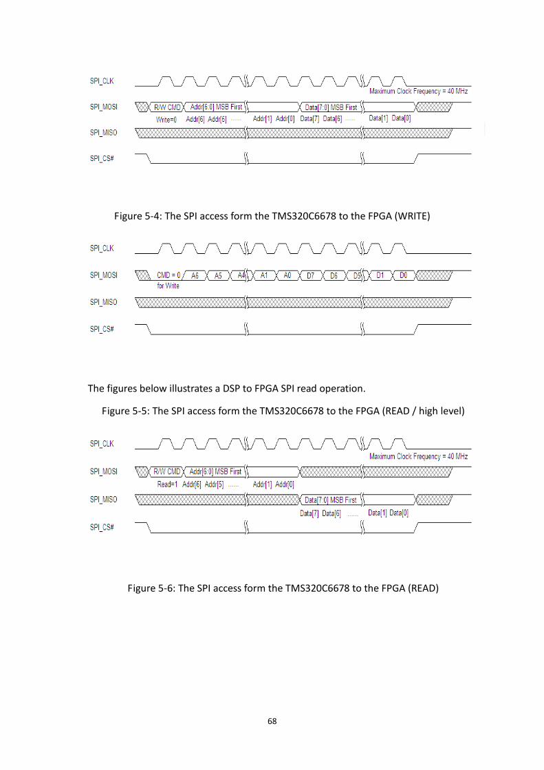
68
Figure 5-4: The SPI access form the TMS320C6678 to the FPGA (WRITE)
The figures below illustrates a DSP to FPGA SPI read operation.
Figure 5-5: The SPI access form the TMS320C6678 to the FPGA (READ / high level)
Figure 5-6: The SPI access form the TMS320C6678 to the FPGA (READ)
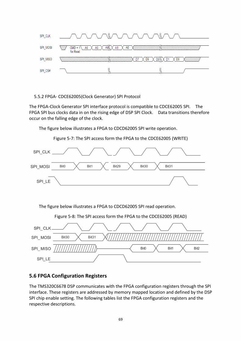
69
5.5.2 FPGA- CDCE62005(Clock Generator) SPI Protocol
The FPGA-Clock Generator SPI interface protocol is compatible to CDCE62005 SPI. The
FPGA SPI bus clocks data in on the rising edge of DSP SPI Clock. Data transitions therefore
occur on the falling edge of the clock.
The figure below illustrates a FPGA to CDCD62005 SPI write operation.
Figure 5-7: The SPI access form the FPGA to the CDCE62005 (WRITE)
The figure below illustrates a FPGA to CDCD62005 SPI read operation.
Figure 5-8: The SPI access form the FPGA to the CDCE62005 (READ)
5.6 FPGA Configuration Registers
The TMS320C6678 DSP communicates with the FPGA configuration registers through the SPI
interface. These registers are addressed by memory mapped location and defined by the DSP
SPI chip enable setting. The following tables list the FPGA configuration registers and the
respective descriptions.
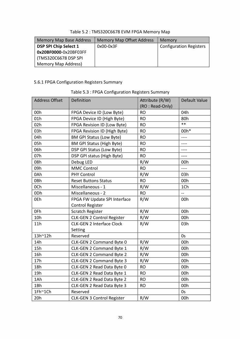
70
Table 5.2 : TMS320C6678 EVM FPGA Memory Map
Memory Map Base Address Memory Map Offset Address Memory
DSP SPI Chip Select 1
0x20BF0000-0x20BF03FF
(TMS320C6678 DSP SPI
Memory Map Address)
0x00-0x3F Configuration Registers
5.6.1 FPGA Configuration Registers Summary
Table 5.3 : FPGA Configuration Registers Summary
Address Offset Definition Attribute (R/W)
(RO : Read-Only)
Default Value
00h FPGA Device ID (Low Byte) RO 04h
01h FPGA Device ID (High Byte) RO 80h
02h FPGA Revision ID (Low Byte) RO **
03h FPGA Revision ID (High Byte) RO 00h*
04h BM GPI Status (Low Byte) RO ----
05h BM GPI Status (High Byte) RO ----
06h DSP GPI Status (Low Byte) RO ----
07h DSP GPI status (High Byte) RO ----
08h Debug LED R/W 00h
09h MMC Control RO ----
0Ah PHY Control R/W 03h
0Bh Reset Buttons Status RO 00h
0Ch Miscellaneous - 1 R/W 1Ch
0Dh Miscellaneous - 2 RO --
0Eh FPGA FW Update SPI Interface
Control Register
R/W 00h
0Fh Scratch Register R/W 00h
10h CLK-GEN 2 Control Register R/W 00h
11h CLK-GEN 2 Interface Clock
Setting
R/W 03h
13h~12h Reserved 0s
14h CLK-GEN 2 Command Byte 0 R/W 00h
15h CLK-GEN 2 Command Byte 1 R/W 00h
16h CLK-GEN 2 Command Byte 2 R/W 00h
17h CLK-GEN 2 Command Byte 3 R/W 00h
18h CLK-GEN 2 Read Data Byte 0 RO 00h
19h CLK-GEN 2 Read Data Byte 1 RO 00h
1Ah CLK-GEN 2 Read Data Byte 2 RO 00h
1Bh CLK-GEN 2 Read Data Byte 3 RO 00h
1Fh~1Ch Reserved 0s
20h CLK-GEN 3 Control Register R/W 00h
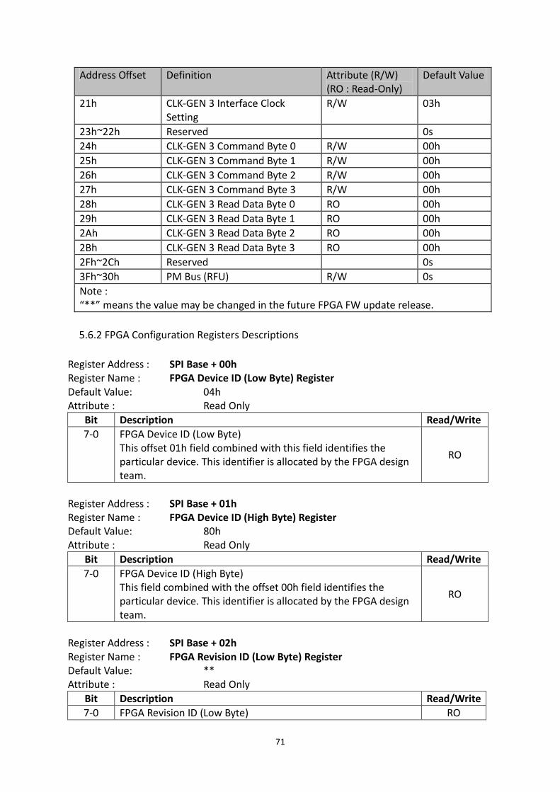
71
Address Offset Definition Attribute (R/W)
(RO : Read-Only)
Default Value
21h CLK-GEN 3 Interface Clock
Setting
R/W 03h
23h~22h Reserved 0s
24h CLK-GEN 3 Command Byte 0 R/W 00h
25h CLK-GEN 3 Command Byte 1 R/W 00h
26h CLK-GEN 3 Command Byte 2 R/W 00h
27h CLK-GEN 3 Command Byte 3 R/W 00h
28h CLK-GEN 3 Read Data Byte 0 RO 00h
29h CLK-GEN 3 Read Data Byte 1 RO 00h
2Ah CLK-GEN 3 Read Data Byte 2 RO 00h
2Bh CLK-GEN 3 Read Data Byte 3 RO 00h
2Fh~2Ch Reserved 0s
3Fh~30h PM Bus (RFU) R/W 0s
Note :
“**” means the value may be changed in the future FPGA FW update release.
5.6.2 FPGA Configuration Registers Descriptions
Register Address : SPI Base + 00h
Register Name : FPGA Device ID (Low Byte) Register
Default Value: 04h
Attribute : Read Only
Bit Description Read/Write
7-0 FPGA Device ID (Low Byte)
This offset 01h field combined with this field identifies the
particular device. This identifier is allocated by the FPGA design
team.
RO
Register Address : SPI Base + 01h
Register Name : FPGA Device ID (High Byte) Register
Default Value: 80h
Attribute : Read Only
Bit Description Read/Write
7-0 FPGA Device ID (High Byte)
This field combined with the offset 00h field identifies the
particular device. This identifier is allocated by the FPGA design
team.
RO
Register Address : SPI Base + 02h
Register Name : FPGA Revision ID (Low Byte) Register
Default Value: **
Attribute : Read Only
Bit Description Read/Write
7-0 FPGA Revision ID (Low Byte) RO
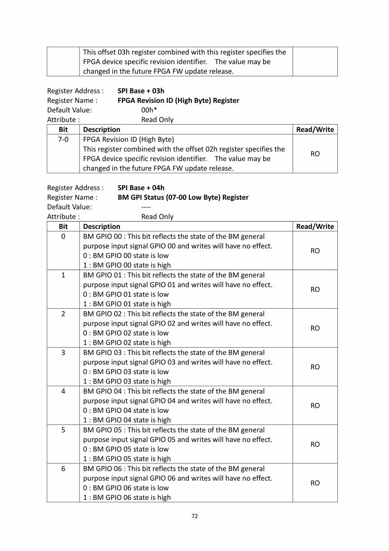
72
This offset 03h register combined with this register specifies the
FPGA device specific revision identifier. The value may be
changed in the future FPGA FW update release.
Register Address : SPI Base + 03h
Register Name : FPGA Revision ID (High Byte) Register
Default Value: 00h*
Attribute : Read Only
Bit Description Read/Write
7-0 FPGA Revision ID (High Byte)
This register combined with the offset 02h register specifies the
FPGA device specific revision identifier. The value may be
changed in the future FPGA FW update release.
RO
Register Address : SPI Base + 04h
Register Name : BM GPI Status (07-00 Low Byte) Register
Default Value: ----
Attribute : Read Only
Bit Description Read/Write
0 BM GPIO 00 : This bit reflects the state of the BM general
purpose input signal GPIO 00 and writes will have no effect.
0 : BM GPIO 00 state is low
1 : BM GPIO 00 state is high
RO
1 BM GPIO 01 : This bit reflects the state of the BM general
purpose input signal GPIO 01 and writes will have no effect.
0 : BM GPIO 01 state is low
1 : BM GPIO 01 state is high
RO
2 BM GPIO 02 : This bit reflects the state of the BM general
purpose input signal GPIO 02 and writes will have no effect.
0 : BM GPIO 02 state is low
1 : BM GPIO 02 state is high
RO
3 BM GPIO 03 : This bit reflects the state of the BM general
purpose input signal GPIO 03 and writes will have no effect.
0 : BM GPIO 03 state is low
1 : BM GPIO 03 state is high
RO
4 BM GPIO 04 : This bit reflects the state of the BM general
purpose input signal GPIO 04 and writes will have no effect.
0 : BM GPIO 04 state is low
1 : BM GPIO 04 state is high
RO
5 BM GPIO 05 : This bit reflects the state of the BM general
purpose input signal GPIO 05 and writes will have no effect.
0 : BM GPIO 05 state is low
1 : BM GPIO 05 state is high
RO
6 BM GPIO 06 : This bit reflects the state of the BM general
purpose input signal GPIO 06 and writes will have no effect.
0 : BM GPIO 06 state is low
1 : BM GPIO 06 state is high
RO
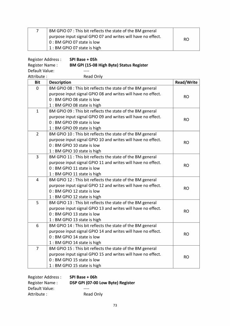
73
7 BM GPIO 07 : This bit reflects the state of the BM general
purpose input signal GPIO 07 and writes will have no effect.
0 : BM GPIO 07 state is low
1 : BM GPIO 07 state is high
RO
Register Address : SPI Base + 05h
Register Name : BM GPI (15-08 High Byte) Status Register
Default Value: ----
Attribute : Read Only
Bit Description Read/Write
0 BM GPIO 08 : This bit reflects the state of the BM general
purpose input signal GPIO 08 and writes will have no effect.
0 : BM GPIO 08 state is low
1 : BM GPIO 08 state is high
RO
1 BM GPIO 09 : This bit reflects the state of the BM general
purpose input signal GPIO 09 and writes will have no effect.
0 : BM GPIO 09 state is low
1 : BM GPIO 09 state is high
RO
2 BM GPIO 10 : This bit reflects the state of the BM general
purpose input signal GPIO 10 and writes will have no effect.
0 : BM GPIO 10 state is low
1 : BM GPIO 10 state is high
RO
3 BM GPIO 11 : This bit reflects the state of the BM general
purpose input signal GPIO 11 and writes will have no effect.
0 : BM GPIO 11 state is low
1 : BM GPIO 11 state is high
RO
4 BM GPIO 12 : This bit reflects the state of the BM general
purpose input signal GPIO 12 and writes will have no effect.
0 : BM GPIO 12 state is low
1 : BM GPIO 12 state is high
RO
5 BM GPIO 13 : This bit reflects the state of the BM general
purpose input signal GPIO 13 and writes will have no effect.
0 : BM GPIO 13 state is low
1 : BM GPIO 13 state is high
RO
6 BM GPIO 14 : This bit reflects the state of the BM general
purpose input signal GPIO 14 and writes will have no effect.
0 : BM GPIO 14 state is low
1 : BM GPIO 14 state is high
RO
7 BM GPIO 15 : This bit reflects the state of the BM general
purpose input signal GPIO 15 and writes will have no effect.
0 : BM GPIO 15 state is low
1 : BM GPIO 15 state is high
RO
Register Address : SPI Base + 06h
Register Name : DSP GPI (07-00 Low Byte) Register
Default Value: ----
Attribute : Read Only
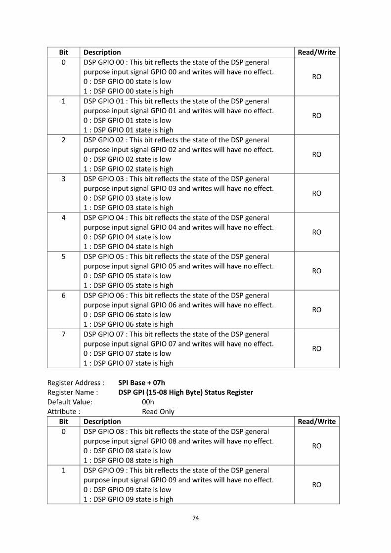
74
Bit Description Read/Write
0 DSP GPIO 00 : This bit reflects the state of the DSP general
purpose input signal GPIO 00 and writes will have no effect.
0 : DSP GPIO 00 state is low
1 : DSP GPIO 00 state is high
RO
1 DSP GPIO 01 : This bit reflects the state of the DSP general
purpose input signal GPIO 01 and writes will have no effect.
0 : DSP GPIO 01 state is low
1 : DSP GPIO 01 state is high
RO
2 DSP GPIO 02 : This bit reflects the state of the DSP general
purpose input signal GPIO 02 and writes will have no effect.
0 : DSP GPIO 02 state is low
1 : DSP GPIO 02 state is high
RO
3 DSP GPIO 03 : This bit reflects the state of the DSP general
purpose input signal GPIO 03 and writes will have no effect.
0 : DSP GPIO 03 state is low
1 : DSP GPIO 03 state is high
RO
4 DSP GPIO 04 : This bit reflects the state of the DSP general
purpose input signal GPIO 04 and writes will have no effect.
0 : DSP GPIO 04 state is low
1 : DSP GPIO 04 state is high
RO
5 DSP GPIO 05 : This bit reflects the state of the DSP general
purpose input signal GPIO 05 and writes will have no effect.
0 : DSP GPIO 05 state is low
1 : DSP GPIO 05 state is high
RO
6 DSP GPIO 06 : This bit reflects the state of the DSP general
purpose input signal GPIO 06 and writes will have no effect.
0 : DSP GPIO 06 state is low
1 : DSP GPIO 06 state is high
RO
7 DSP GPIO 07 : This bit reflects the state of the DSP general
purpose input signal GPIO 07 and writes will have no effect.
0 : DSP GPIO 07 state is low
1 : DSP GPIO 07 state is high
RO
Register Address : SPI Base + 07h
Register Name : DSP GPI (15-08 High Byte) Status Register
Default Value: 00h
Attribute : Read Only
Bit Description Read/Write
0 DSP GPIO 08 : This bit reflects the state of the DSP general
purpose input signal GPIO 08 and writes will have no effect.
0 : DSP GPIO 08 state is low
1 : DSP GPIO 08 state is high
RO
1 DSP GPIO 09 : This bit reflects the state of the DSP general
purpose input signal GPIO 09 and writes will have no effect.
0 : DSP GPIO 09 state is low
1 : DSP GPIO 09 state is high
RO
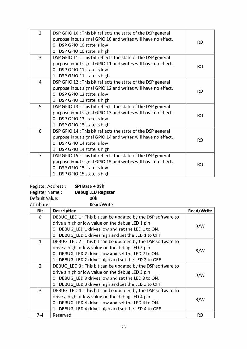
75
2 DSP GPIO 10 : This bit reflects the state of the DSP general
purpose input signal GPIO 10 and writes will have no effect.
0 : DSP GPIO 10 state is low
1 : DSP GPIO 10 state is high
RO
3 DSP GPIO 11 : This bit reflects the state of the DSP general
purpose input signal GPIO 11 and writes will have no effect.
0 : DSP GPIO 11 state is low
1 : DSP GPIO 11 state is high
RO
4 DSP GPIO 12 : This bit reflects the state of the DSP general
purpose input signal GPIO 12 and writes will have no effect.
0 : DSP GPIO 12 state is low
1 : DSP GPIO 12 state is high
RO
5 DSP GPIO 13 : This bit reflects the state of the DSP general
purpose input signal GPIO 13 and writes will have no effect.
0 : DSP GPIO 13 state is low
1 : DSP GPIO 13 state is high
RO
6 DSP GPIO 14 : This bit reflects the state of the DSP general
purpose input signal GPIO 14 and writes will have no effect.
0 : DSP GPIO 14 state is low
1 : DSP GPIO 14 state is high
RO
7 DSP GPIO 15 : This bit reflects the state of the DSP general
purpose input signal GPIO 15 and writes will have no effect.
0 : DSP GPIO 15 state is low
1 : DSP GPIO 15 state is high
RO
Register Address : SPI Base + 08h
Register Name : Debug LED Register
Default Value: 00h
Attribute : Read/Write
Bit Description Read/Write
0 DEBUG_LED 1 : This bit can be updated by the DSP software to
drive a high or low value on the debug LED 1 pin.
0 : DEBUG_LED 1 drives low and set the LED 1 to ON.
1 : DEBUG_LED 1 drives high and set the LED 1 to OFF.
R/W
1 DEBUG_LED 2 : This bit can be updated by the DSP software to
drive a high or low value on the debug LED 2 pin.
0 : DEBUG_LED 2 drives low and set the LED 2 to ON.
1 : DEBUG_LED 2 drives high and set the LED 2 to OFF.
R/W
2 DEBUG_LED 3 : This bit can be updated by the DSP software to
drive a high or low value on the debug LED 3 pin
0 : DEBUG_LED 3 drives low and set the LED 3 to ON.
1 : DEBUG_LED 3 drives high and set the LED 3 to OFF.
R/W
3 DEBUG_LED 4 : This bit can be updated by the DSP software to
drive a high or low value on the debug LED 4 pin
0 : DEBUG_LED 4 drives low and set the LED 4 to ON.
1 : DEBUG_LED 4 drives high and set the LED 4 to OFF.
R/W
7-4 Reserved RO
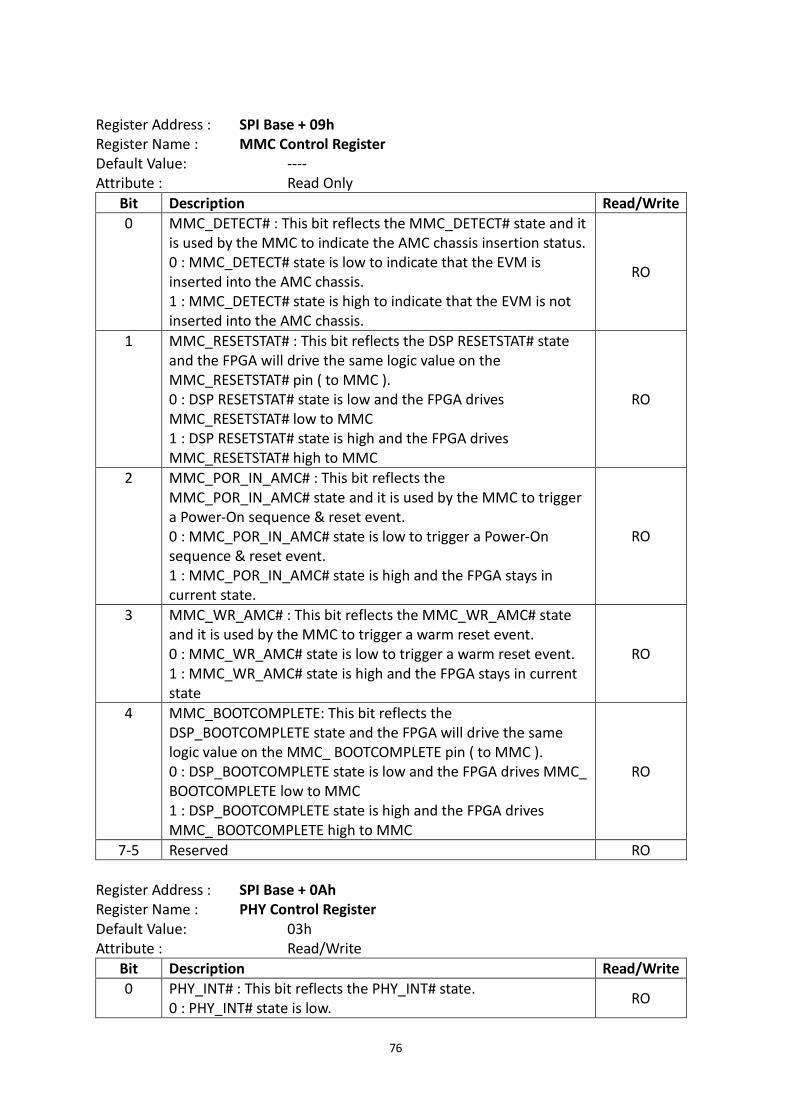
76
Register Address : SPI Base + 09h
Register Name : MMC Control Register
Default Value: ----
Attribute : Read Only
Bit Description Read/Write
0 MMC_DETECT# : This bit reflects the MMC_DETECT# state and it
is used by the MMC to indicate the AMC chassis insertion status.
0 : MMC_DETECT# state is low to indicate that the EVM is
inserted into the AMC chassis.
1 : MMC_DETECT# state is high to indicate that the EVM is not
inserted into the AMC chassis.
RO
1 MMC_RESETSTAT# : This bit reflects the DSP RESETSTAT# state
and the FPGA will drive the same logic value on the
MMC_RESETSTAT# pin ( to MMC ).
0 : DSP RESETSTAT# state is low and the FPGA drives
MMC_RESETSTAT# low to MMC
1 : DSP RESETSTAT# state is high and the FPGA drives
MMC_RESETSTAT# high to MMC
RO
2 MMC_POR_IN_AMC# : This bit reflects the
MMC_POR_IN_AMC# state and it is used by the MMC to trigger
a Power-On sequence & reset event.
0 : MMC_POR_IN_AMC# state is low to trigger a Power-On
sequence & reset event.
1 : MMC_POR_IN_AMC# state is high and the FPGA stays in
current state.
RO
3 MMC_WR_AMC# : This bit reflects the MMC_WR_AMC# state
and it is used by the MMC to trigger a warm reset event.
0 : MMC_WR_AMC# state is low to trigger a warm reset event.
1 : MMC_WR_AMC# state is high and the FPGA stays in current
state
RO
4 MMC_BOOTCOMPLETE: This bit reflects the
DSP_BOOTCOMPLETE state and the FPGA will drive the same
logic value on the MMC_ BOOTCOMPLETE pin ( to MMC ).
0 : DSP_BOOTCOMPLETE state is low and the FPGA drives MMC_
BOOTCOMPLETE low to MMC
1 : DSP_BOOTCOMPLETE state is high and the FPGA drives
MMC_ BOOTCOMPLETE high to MMC
RO
7-5 Reserved RO
Register Address : SPI Base + 0Ah
Register Name : PHY Control Register
Default Value: 03h
Attribute : Read/Write
Bit Description Read/Write
0 PHY_INT# : This bit reflects the PHY_INT# state.
0 : PHY_INT# state is low. RO
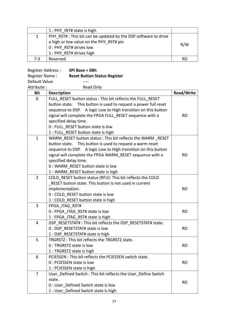
77
1 : PHY_INT# state is high.
1 PHY_RST# : This bit can be updated by the DSP software to drive
a high or low value on the PHY_RST# pin
0 : PHY_RST# drives low
1 : PHY_RST# drives high
R/W
7-3 Reserved RO
Register Address : SPI Base + 0Bh
Register Name : Reset Button Status Register
Default Value: ----
Attribute : Read Only
Bit Description Read/Write
0 FULL_RESET button status : This bit reflects the FULL_RESET
button state. This button is used to request a power full reset
sequence to DSP. A logic Low to High transition on this button
signal will complete the FPGA FULL_RESET sequence with a
specified delay time.
0 : FULL_RESET button state is low
1 : FULL_RESET button state is high
RO
1 WARM_RESET button status : This bit reflects the WARM _RESET
button state. This button is used to request a warm reset
sequence to DSP. A logic Low to High transition on this button
signal will complete the FPGA WARM_RESET sequence with a
specified delay time.
0 : WARM_RESET button state is low
1 : WARM_RESET button state is high
RO
2 COLD_RESET button status (RFU): This bit reflects the COLD
_RESET button state. This button is not used in current
implementation.
0 : COLD_RESET button state is low
1 : COLD_RESET button state is high
RO
3 FPGA_JTAG_RST#
0 : FPGA_JTAG_RST# state is low
1 : FPGA_JTAG_RST# state is high
RO
4 DSP_RESETSTAT# : This bit reflects the DSP_RESETSTAT# state.
0 : DSP_RESETSTAT# state is low
1 : DSP_RESETSTAT# state is high
RO
5 TRGRSTZ : This bit reflects the TRGRSTZ state.
0 : TRGRSTZ state is low
1 : TRGRSTZ state is high
RO
6 PCIESSEN : This bit reflects the PCIESSEN switch state.
0 : PCIESSEN state is low
1 : PCIESSEN state is high
RO
7 User_Defined Switch : This bit reflects the User_Define Switch
state.
0 : User_Defined Switch state is low
1 : User_Defined Switch state is high
RO
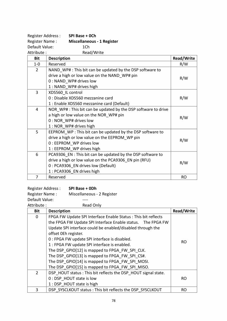
78
Register Address : SPI Base + 0Ch
Register Name : Miscellaneous - 1 Register
Default Value: 1Ch
Attribute : Read/Write
Bit Description Read/Write
1-0 Reserved R/W
2 NAND_WP# : This bit can be updated by the DSP software to
drive a high or low value on the NAND_WP# pin
0 : NAND_WP# drives low
1 : NAND_WP# drives high
R/W
3 XDS560_IL control
0 : Disable XDS560 mezzanine card
1 : Enable XDS560 mezzanine card (Default)
R/W
4 NOR_WP# : This bit can be updated by the DSP software to drive
a high or low value on the NOR_WP# pin
0 : NOR_WP# drives low
1 : NOR_WP# drives high
R/W
5 EEPROM_WP : This bit can be updated by the DSP software to
drive a high or low value on the EEPROM_WP pin
0 : EEPROM_WP drives low
1 : EEPROM_WP drives high
R/W
6 PCA9306_EN : This bit can be updated by the DSP software to
drive a high or low value on the PCA9306_EN pin (RFU)
0 : PCA9306_EN drives low (Default)
1 : PCA9306_EN drives high
R/W
7 Reserved RO
Register Address : SPI Base + 0Dh
Register Name : Miscellaneous - 2 Register
Default Value: ----
Attribute : Read Only
Bit Description Read/Write
0 FPGA FW Update SPI Interface Enable Status : This bit reflects
the FPGA FW Update SPI Interface Enable status. The FPGA FW
Update SPI interface could be enabled/disabled through the
offset 0Eh register.
0 : FPGA FW update SPI interface is disabled.
1 : FPGA FW update SPI interface is enabled.
The DSP_GPIO[12] is mapped to FPGA_FW_SPI_CLK.
The DSP_GPIO[13] is mapped to FPGA_FW_SPI_CS#.
The DSP_GPIO[14] is mapped to FPGA_FW_SPI_MOSI.
The DSP_GPIO[15] is mapped to FPGA_FW_SPI_MISO.
RO
2 DSP_HOUT status : This bit reflects the DSP_HOUT signal state.
0 : DSP_HOUT state is low
1 : DSP_HOUT state is high
RO
3 DSP_SYSCLKOUT status : This bit reflects the DSP_SYSCLKOUT RO
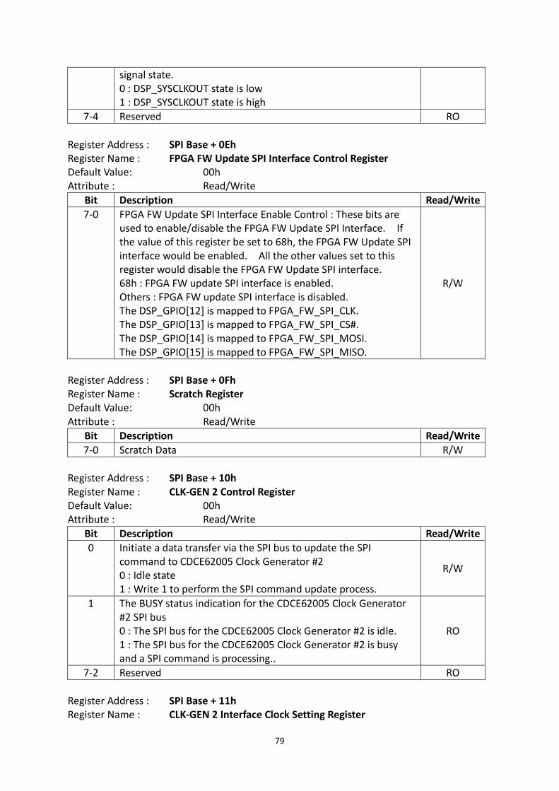
79
signal state.
0 : DSP_SYSCLKOUT state is low
1 : DSP_SYSCLKOUT state is high
7-4 Reserved RO
Register Address : SPI Base + 0Eh
Register Name : FPGA FW Update SPI Interface Control Register
Default Value: 00h
Attribute : Read/Write
Bit Description Read/Write
7-0 FPGA FW Update SPI Interface Enable Control : These bits are
used to enable/disable the FPGA FW Update SPI Interface. If
the value of this register be set to 68h, the FPGA FW Update SPI
interface would be enabled. All the other values set to this
register would disable the FPGA FW Update SPI interface.
68h : FPGA FW update SPI interface is enabled.
Others : FPGA FW update SPI interface is disabled.
The DSP_GPIO[12] is mapped to FPGA_FW_SPI_CLK.
The DSP_GPIO[13] is mapped to FPGA_FW_SPI_CS#.
The DSP_GPIO[14] is mapped to FPGA_FW_SPI_MOSI.
The DSP_GPIO[15] is mapped to FPGA_FW_SPI_MISO.
R/W
Register Address : SPI Base + 0Fh
Register Name : Scratch Register
Default Value: 00h
Attribute : Read/Write
Bit Description Read/Write
7-0 Scratch Data R/W
Register Address : SPI Base + 10h
Register Name : CLK-GEN 2 Control Register
Default Value: 00h
Attribute : Read/Write
Bit Description Read/Write
0 Initiate a data transfer via the SPI bus to update the SPI
command to CDCE62005 Clock Generator #2
0 : Idle state
1 : Write 1 to perform the SPI command update process.
R/W
1 The BUSY status indication for the CDCE62005 Clock Generator
#2 SPI bus
0 : The SPI bus for the CDCE62005 Clock Generator #2 is idle.
1 : The SPI bus for the CDCE62005 Clock Generator #2 is busy
and a SPI command is processing..
RO
7-2 Reserved RO
Register Address : SPI Base + 11h
Register Name : CLK-GEN 2 Interface Clock Setting Register
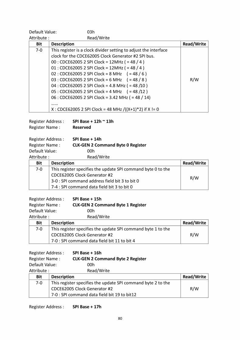
80
Default Value: 03h
Attribute : Read/Write
Bit Description Read/Write
7-0 This register is a clock divider setting to adjust the interface
clock for the CDCE62005 Clock Generator #2 SPI bus.
00 : CDCE62005 2 SPI Clock = 12MHz ( = 48 / 4 )
01 : CDCE62005 2 SPI Clock = 12MHz ( = 48 / 4 )
02 : CDCE62005 2 SPI Clock = 8 MHz ( = 48 / 6 )
03 : CDCE62005 2 SPI Clock = 6 MHz ( = 48 / 8 )
04 : CDCE62005 2 SPI Clock = 4.8 MHz ( = 48 /10 )
05 : CDCE62005 2 SPI Clock = 4 MHz ( = 48 /12 )
06 : CDCE62005 2 SPI Clock = 3.42 MHz ( = 48 / 14)
……
X : CDCE62005 2 SPI Clock = 48 MHz /((X+1)*2) if X != 0
R/W
Register Address : SPI Base + 12h ~ 13h
Register Name : Reserved
Register Address : SPI Base + 14h
Register Name : CLK-GEN 2 Command Byte 0 Register
Default Value: 00h
Attribute : Read/Write
Bit Description Read/Write
7-0 This register specifies the update SPI command byte 0 to the
CDCE62005 Clock Generator #2
3-0 : SPI command address field bit 3 to bit 0
7-4 : SPI command data field bit 3 to bit 0
R/W
Register Address : SPI Base + 15h
Register Name : CLK-GEN 2 Command Byte 1 Register
Default Value: 00h
Attribute : Read/Write
Bit Description Read/Write
7-0 This register specifies the update SPI command byte 1 to the
CDCE62005 Clock Generator #2
7-0 : SPI command data field bit 11 to bit 4
R/W
Register Address : SPI Base + 16h
Register Name : CLK-GEN 2 Command Byte 2 Register
Default Value: 00h
Attribute : Read/Write
Bit Description Read/Write
7-0 This register specifies the update SPI command byte 2 to the
CDCE62005 Clock Generator #2
7-0 : SPI command data field bit 19 to bit12
R/W
Register Address : SPI Base + 17h
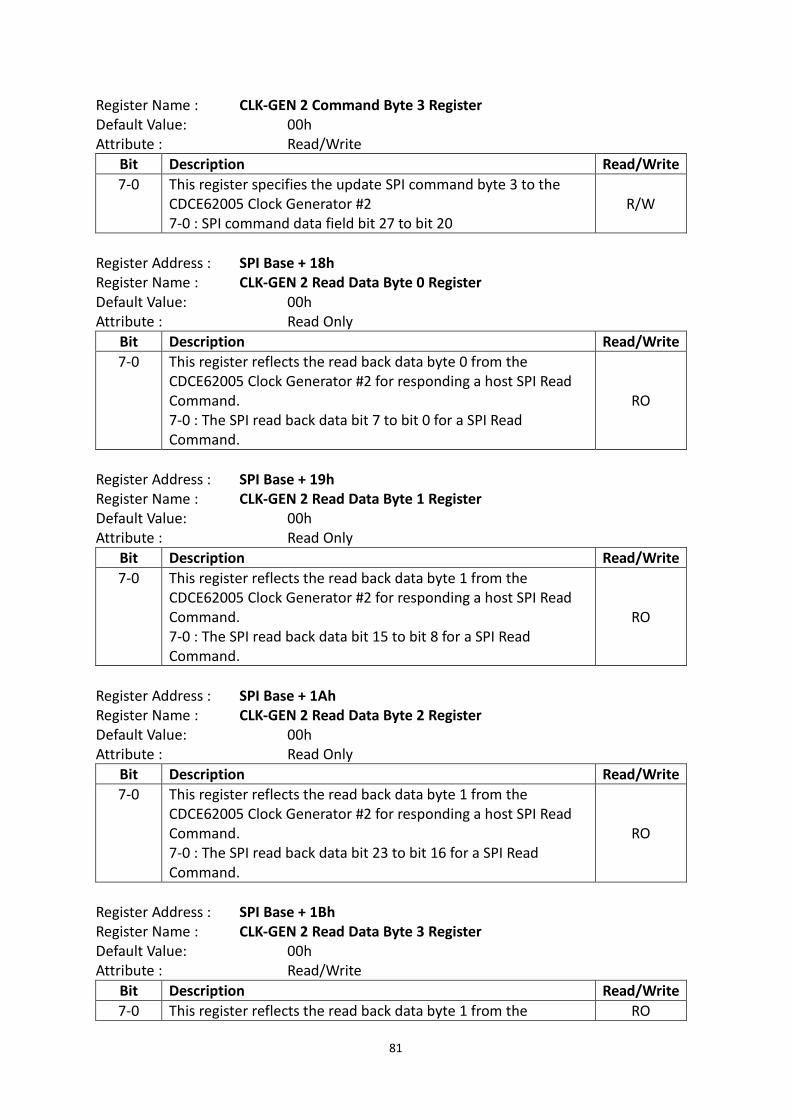
81
Register Name : CLK-GEN 2 Command Byte 3 Register
Default Value: 00h
Attribute : Read/Write
Bit Description Read/Write
7-0 This register specifies the update SPI command byte 3 to the
CDCE62005 Clock Generator #2
7-0 : SPI command data field bit 27 to bit 20
R/W
Register Address : SPI Base + 18h
Register Name : CLK-GEN 2 Read Data Byte 0 Register
Default Value: 00h
Attribute : Read Only
Bit Description Read/Write
7-0 This register reflects the read back data byte 0 from the
CDCE62005 Clock Generator #2 for responding a host SPI Read
Command.
7-0 : The SPI read back data bit 7 to bit 0 for a SPI Read
Command.
RO
Register Address : SPI Base + 19h
Register Name : CLK-GEN 2 Read Data Byte 1 Register
Default Value: 00h
Attribute : Read Only
Bit Description Read/Write
7-0 This register reflects the read back data byte 1 from the
CDCE62005 Clock Generator #2 for responding a host SPI Read
Command.
7-0 : The SPI read back data bit 15 to bit 8 for a SPI Read
Command.
RO
Register Address : SPI Base + 1Ah
Register Name : CLK-GEN 2 Read Data Byte 2 Register
Default Value: 00h
Attribute : Read Only
Bit Description Read/Write
7-0 This register reflects the read back data byte 1 from the
CDCE62005 Clock Generator #2 for responding a host SPI Read
Command.
7-0 : The SPI read back data bit 23 to bit 16 for a SPI Read
Command.
RO
Register Address : SPI Base + 1Bh
Register Name : CLK-GEN 2 Read Data Byte 3 Register
Default Value: 00h
Attribute : Read/Write
Bit Description Read/Write
7-0 This register reflects the read back data byte 1 from the RO
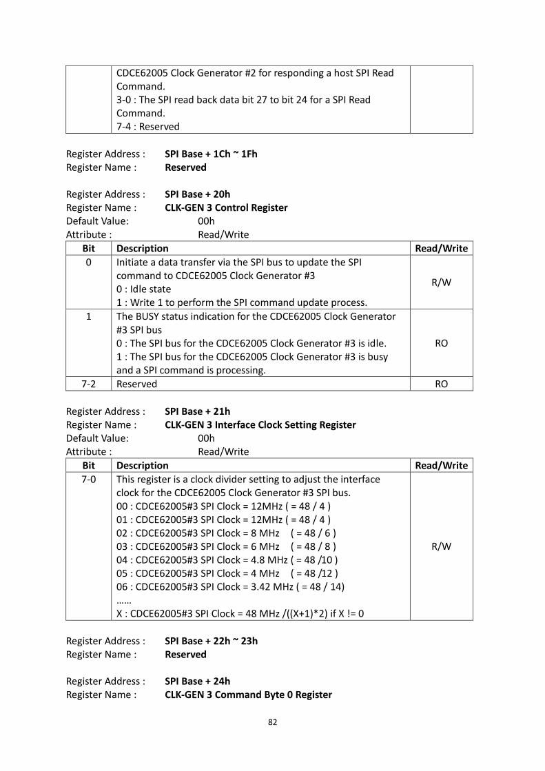
82
CDCE62005 Clock Generator #2 for responding a host SPI Read
Command.
3-0 : The SPI read back data bit 27 to bit 24 for a SPI Read
Command.
7-4 : Reserved
Register Address : SPI Base + 1Ch ~ 1Fh
Register Name : Reserved
Register Address : SPI Base + 20h
Register Name : CLK-GEN 3 Control Register
Default Value: 00h
Attribute : Read/Write
Bit Description Read/Write
0 Initiate a data transfer via the SPI bus to update the SPI
command to CDCE62005 Clock Generator #3
0 : Idle state
1 : Write 1 to perform the SPI command update process.
R/W
1 The BUSY status indication for the CDCE62005 Clock Generator
#3 SPI bus
0 : The SPI bus for the CDCE62005 Clock Generator #3 is idle.
1 : The SPI bus for the CDCE62005 Clock Generator #3 is busy
and a SPI command is processing.
RO
7-2 Reserved RO
Register Address : SPI Base + 21h
Register Name : CLK-GEN 3 Interface Clock Setting Register
Default Value: 00h
Attribute : Read/Write
Bit Description Read/Write
7-0 This register is a clock divider setting to adjust the interface
clock for the CDCE62005 Clock Generator #3 SPI bus.
00 : CDCE62005#3 SPI Clock = 12MHz ( = 48 / 4 )
01 : CDCE62005#3 SPI Clock = 12MHz ( = 48 / 4 )
02 : CDCE62005#3 SPI Clock = 8 MHz ( = 48 / 6 )
03 : CDCE62005#3 SPI Clock = 6 MHz ( = 48 / 8 )
04 : CDCE62005#3 SPI Clock = 4.8 MHz ( = 48 /10 )
05 : CDCE62005#3 SPI Clock = 4 MHz ( = 48 /12 )
06 : CDCE62005#3 SPI Clock = 3.42 MHz ( = 48 / 14)
……
X : CDCE62005#3 SPI Clock = 48 MHz /((X+1)*2) if X != 0
R/W
Register Address : SPI Base + 22h ~ 23h
Register Name : Reserved
Register Address : SPI Base + 24h
Register Name : CLK-GEN 3 Command Byte 0 Register
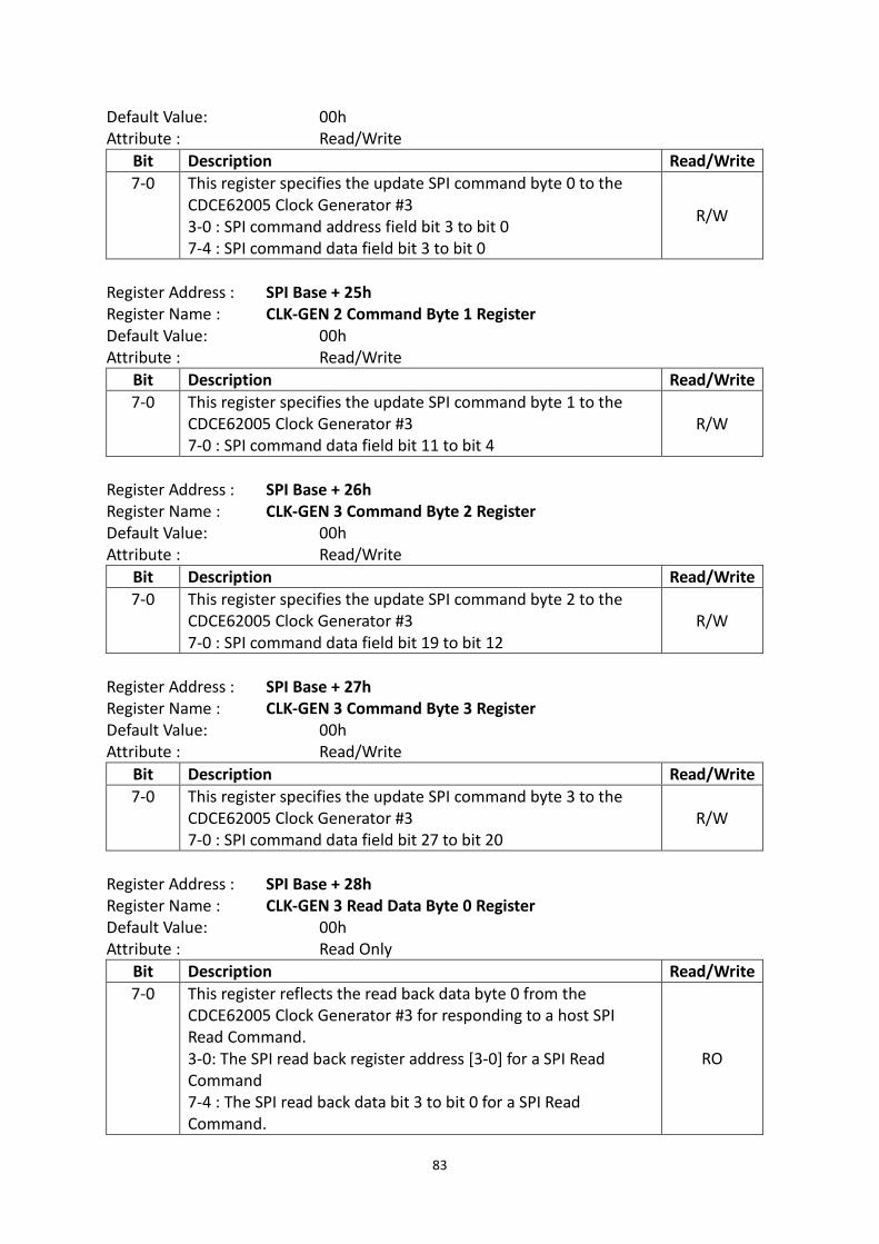
83
Default Value: 00h
Attribute : Read/Write
Bit Description Read/Write
7-0 This register specifies the update SPI command byte 0 to the
CDCE62005 Clock Generator #3
3-0 : SPI command address field bit 3 to bit 0
7-4 : SPI command data field bit 3 to bit 0
R/W
Register Address : SPI Base + 25h
Register Name : CLK-GEN 2 Command Byte 1 Register
Default Value: 00h
Attribute : Read/Write
Bit Description Read/Write
7-0 This register specifies the update SPI command byte 1 to the
CDCE62005 Clock Generator #3
7-0 : SPI command data field bit 11 to bit 4
R/W
Register Address : SPI Base + 26h
Register Name : CLK-GEN 3 Command Byte 2 Register
Default Value: 00h
Attribute : Read/Write
Bit Description Read/Write
7-0 This register specifies the update SPI command byte 2 to the
CDCE62005 Clock Generator #3
7-0 : SPI command data field bit 19 to bit 12
R/W
Register Address : SPI Base + 27h
Register Name : CLK-GEN 3 Command Byte 3 Register
Default Value: 00h
Attribute : Read/Write
Bit Description Read/Write
7-0 This register specifies the update SPI command byte 3 to the
CDCE62005 Clock Generator #3
7-0 : SPI command data field bit 27 to bit 20
R/W
Register Address : SPI Base + 28h
Register Name : CLK-GEN 3 Read Data Byte 0 Register
Default Value: 00h
Attribute : Read Only
Bit Description Read/Write
7-0 This register reflects the read back data byte 0 from the
CDCE62005 Clock Generator #3 for responding to a host SPI
Read Command.
3-0: The SPI read back register address [3-0] for a SPI Read
Command
7-4 : The SPI read back data bit 3 to bit 0 for a SPI Read
Command.
RO
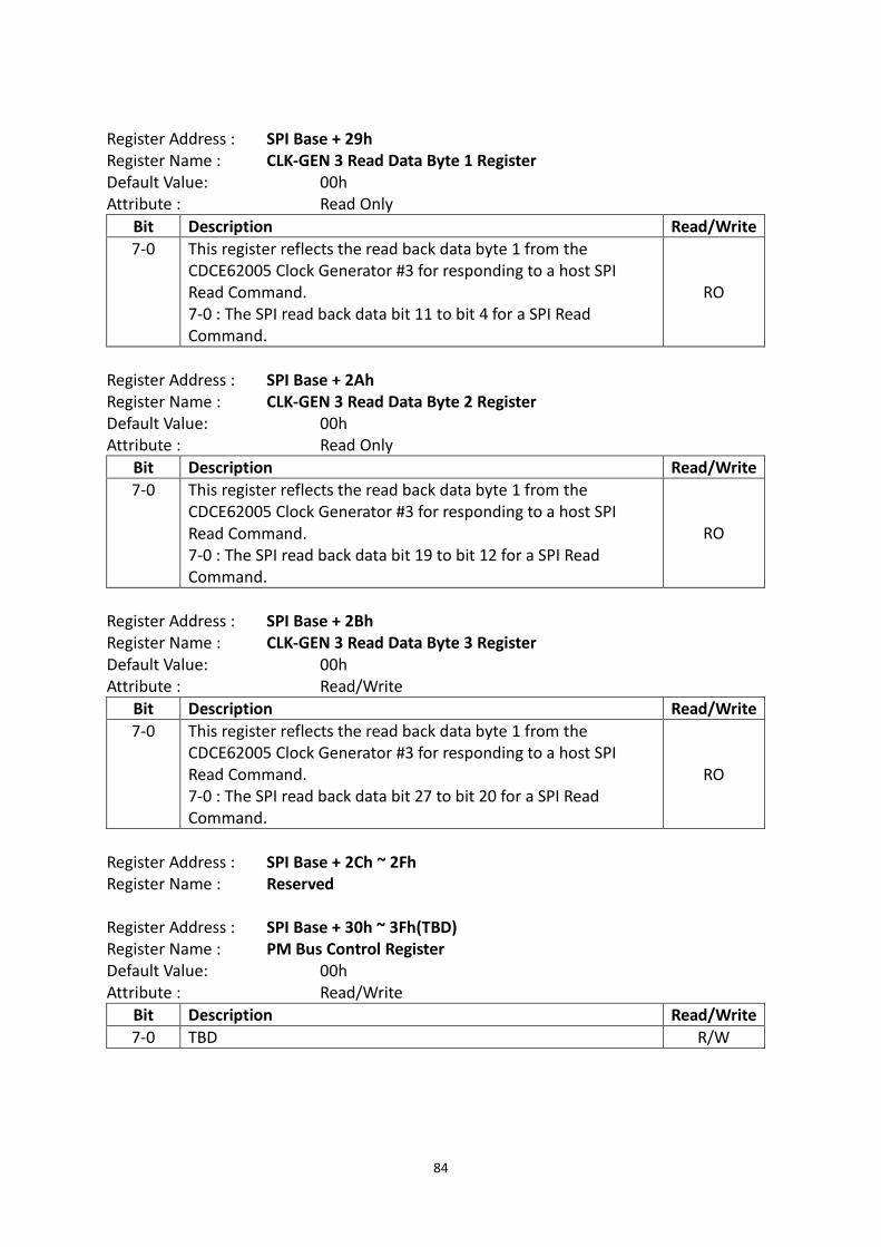
84
Register Address : SPI Base + 29h
Register Name : CLK-GEN 3 Read Data Byte 1 Register
Default Value: 00h
Attribute : Read Only
Bit Description Read/Write
7-0 This register reflects the read back data byte 1 from the
CDCE62005 Clock Generator #3 for responding to a host SPI
Read Command.
7-0 : The SPI read back data bit 11 to bit 4 for a SPI Read
Command.
RO
Register Address : SPI Base + 2Ah
Register Name : CLK-GEN 3 Read Data Byte 2 Register
Default Value: 00h
Attribute : Read Only
Bit Description Read/Write
7-0 This register reflects the read back data byte 1 from the
CDCE62005 Clock Generator #3 for responding to a host SPI
Read Command.
7-0 : The SPI read back data bit 19 to bit 12 for a SPI Read
Command.
RO
Register Address : SPI Base + 2Bh
Register Name : CLK-GEN 3 Read Data Byte 3 Register
Default Value: 00h
Attribute : Read/Write
Bit Description Read/Write
7-0 This register reflects the read back data byte 1 from the
CDCE62005 Clock Generator #3 for responding to a host SPI
Read Command.
7-0 : The SPI read back data bit 27 to bit 20 for a SPI Read
Command.
RO
Register Address : SPI Base + 2Ch ~ 2Fh
Register Name : Reserved
Register Address : SPI Base + 30h ~ 3Fh(TBD)
Register Name : PM Bus Control Register
Default Value: 00h
Attribute : Read/Write
Bit Description Read/Write
7-0 TBD R/W
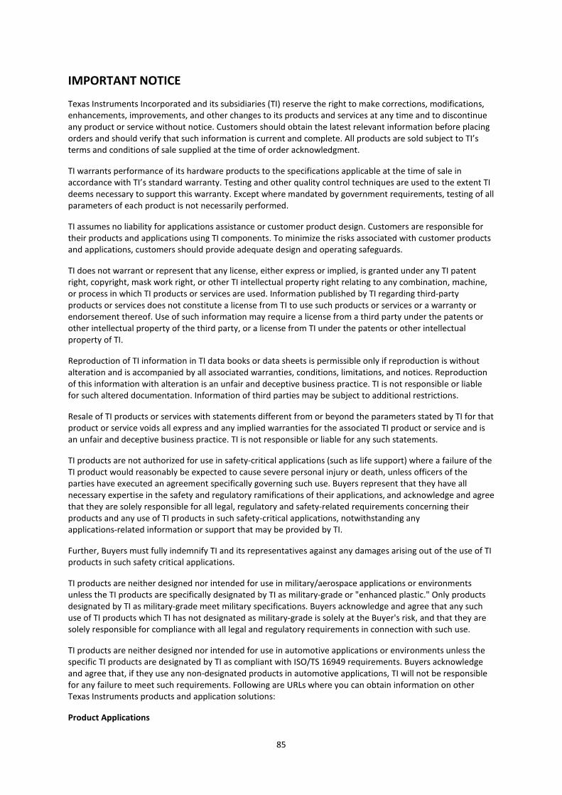
85
IMPORTANT NOTICE
Texas Instruments Incorporated and its subsidiaries (TI) reserve the right to make corrections, modifications,
enhancements, improvements, and other changes to its products and services at any time and to discontinue
any product or service without notice. Customers should obtain the latest relevant information before placing
orders and should verify that such information is current and complete. All products are sold subject to TI’s
terms and conditions of sale supplied at the time of order acknowledgment.
TI warrants performance of its hardware products to the specifications applicable at the time of sale in
accordance with TI’s standard warranty. Testing and other quality control techniques are used to the extent TI
deems necessary to support this warranty. Except where mandated by government requirements, testing of all
parameters of each product is not necessarily performed.
TI assumes no liability for applications assistance or customer product design. Customers are responsible for
their products and applications using TI components. To minimize the risks associated with customer products
and applications, customers should provide adequate design and operating safeguards.
TI does not warrant or represent that any license, either express or implied, is granted under any TI patent
right, copyright, mask work right, or other TI intellectual property right relating to any combination, machine,
or process in which TI products or services are used. Information published by TI regarding third-party
products or services does not constitute a license from TI to use such products or services or a warranty or
endorsement thereof. Use of such information may require a license from a third party under the patents or
other intellectual property of the third party, or a license from TI under the patents or other intellectual
property of TI.
Reproduction of TI information in TI data books or data sheets is permissible only if reproduction is without
alteration and is accompanied by all associated warranties, conditions, limitations, and notices. Reproduction
of this information with alteration is an unfair and deceptive business practice. TI is not responsible or liable
for such altered documentation. Information of third parties may be subject to additional restrictions.
Resale of TI products or services with statements different from or beyond the parameters stated by TI for that
product or service voids all express and any implied warranties for the associated TI product or service and is
an unfair and deceptive business practice. TI is not responsible or liable for any such statements.
TI products are not authorized for use in safety-critical applications (such as life support) where a failure of the
TI product would reasonably be expected to cause severe personal injury or death, unless officers of the
parties have executed an agreement specifically governing such use. Buyers represent that they have all
necessary expertise in the safety and regulatory ramifications of their applications, and acknowledge and agree
that they are solely responsible for all legal, regulatory and safety-related requirements concerning their
products and any use of TI products in such safety-critical applications, notwithstanding any
applications-related information or support that may be provided by TI.
Further, Buyers must fully indemnify TI and its representatives against any damages arising out of the use of TI
products in such safety critical applications.
TI products are neither designed nor intended for use in military/aerospace applications or environments
unless the TI products are specifically designated by TI as military-grade or "enhanced plastic." Only products
designated by TI as military-grade meet military specifications. Buyers acknowledge and agree that any such
use of TI products which TI has not designated as military-grade is solely at the Buyer's risk, and that they are
solely responsible for compliance with all legal and regulatory requirements in connection with such use.
TI products are neither designed nor intended for use in automotive applications or environments unless the
specific TI products are designated by TI as compliant with ISO/TS 16949 requirements. Buyers acknowledge
and agree that, if they use any non-designated products in automotive applications, TI will not be responsible
for any failure to meet such requirements. Following are URLs where you can obtain information on other
Texas Instruments products and application solutions:
Product Applications

86
Amplifiers amplifier.ti.com Audio www.ti.com/audio
Data Converters dataconverter.ti.com Automotive www.ti.com/automotive
DSP dsp.ti.com Broadband www.ti.com/broadband
Clocks and Timers www.ti.com/clocks Digital Control www.ti.com/digitalcontrol
Interface interface.ti.com Medical www.ti.com/medical
Logic logic.ti.com Military www.ti.com/military
Power Mgmt power.ti.com Optical Networking www.ti.com/opticalnetwork
Microcontrollers microcontroller.ti.com Security www.ti.com/security
RFID www.ti-rfid.com Telephony www.ti.com/telephony
RF/IF and ZigBee® Solutions www.ti.com/lprf Video & Imaging www.ti.com/video
Wireless www.ti.com/wireless
Mailing Address: Texas Instruments, Post Office Box 655303, Dallas, Texas 75265
Copyright © 2010, Texas Instruments Incorporated