Embed Size (px)
Citation preview

TPDxF202 Four or Six-Channel EMI Filter With ESD Protection For LCD Display
1 Features• Four or six-channel EMI filtering and ESD
protection for data lines• Excellent filter performance
– > 40-dB attenuation at 1 GHz to 3G Hz– –3-dB bandwidth at 108 MHz– 70-dB crosstalk attenuation at 100 MHz
• Exceeds IEC 61000-4-2 (Level 4) ESD protectionrequirements– ±25-kV IEC 61000-4-2 contact discharge– ±25-kV IEC 61000-4-2 air-gap discharge– ±15-kV human body model (HBM)
• Pi-style C-R-C filter configuration offers symmetricfilter performance(R = 100 Ω, CTOTAL = 30 pF)
• Low 10-nA leakage current• Space-saving DSBGA package and flow-through
pin mapping provide optimum performance inportable applications
2 Applications• End equipment:
– LCD displays– Memory interface– Keypads– Portables
• Interfaces:– DVI– VGA, SVGA– SIM cards– Data lines
3 DescriptionThe TPDxF202 devices are four or six-channel EMIfilters, designed particularly to suppress EMI noise inthe cell phone and other portable applications. Thesefilters also provide a Transient Voltage Suppressor(TVS) diode circuit for Electrostatic Discharge (ESD)protection which prevents damage to the applicationwhen subjected to ESD stress far exceeding IEC61000-4-2 (Level 4). The pi-style C-R-C filter providessymmetric filter performance in the data lines to andfrom either side of the filter.
Due to the tiny parasitics of the DSBGA package, theTPDxF202 filters provide excellent signal attenuation(–40 dB at 1 GHz) at the typical cell-phone carrierfrequency ranges.
The ultra thin (0.3-mm package height, when mountedon board) space-saving YFU package enables theTPDxF202 devices to mount on the printed-circuit-boards where height is a key constraint.
The TPDxF202 devices are specified for –40°C to85°C operation.
A typical application for TPDxF202 devices are inportable equipment with DVI, VGA, SVGA, SIM Card,and other data interfaces.
Device Information(1)
PART NUMBER PACKAGE BODY SIZE (NOM)TPD4F202 DSBGA (10) 1.06 mm × 1.57 mm
TPD6F202 DSBGA (15) 1.06 mm × 2.36 mm
(1) For all available packages, see the orderable addendum atthe end of the data sheet.
Functional Block Diagram
TPD4F202, TPD6F202SLLS800B – JUNE 2010 – REVISED MAY 2021
An IMPORTANT NOTICE at the end of this data sheet addresses availability, warranty, changes, use in safety-critical applications,intellectual property matters and other important disclaimers. PRODUCTION DATA.

Table of Contents1 Features............................................................................12 Applications..................................................................... 13 Description.......................................................................14 Revision History.............................................................. 25 Pin Configuration and Functions...................................36 Specifications.................................................................. 5
6.1 Absolute Maximum Ratings........................................ 56.2 ESD Ratings — JEDEC.............................................. 56.3 ESD Ratings — IEC....................................................56.4 Recommended Operating Conditions.........................56.5 Thermal Information....................................................56.6 Electrical Characteristics.............................................66.7 Typical Characteristics................................................ 7
7 Detailed Description........................................................87.1 Overview..................................................................... 87.2 Functional Block Diagram........................................... 87.3 Feature Description.....................................................8
7.4 Device Functional Modes............................................88 Application and Implementation.................................... 9
8.1 Application Information............................................... 98.2 Typical Application...................................................... 9
9 Power Supply Recommendations................................1010 Layout........................................................................... 11
10.1 Layout Guidelines................................................... 1110.2 Layout Example...................................................... 11
11 Device and Documentation Support..........................1211.1 Documentation Support.......................................... 1211.2 Related Links.......................................................... 1211.3 Support Resources................................................. 1211.4 Trademarks............................................................. 1211.5 Electrostatic Discharge Caution.............................. 1211.6 Glossary.................................................................. 12
12 Mechanical, Packaging, and OrderableInformation.................................................................... 12
4 Revision HistoryNOTE: Page numbers for previous revisions may differ from page numbers in the current version.
Changes from Revision A (November 2015) to Revision B (May 2021) Page• Updated the numbering format for tables, figures, and cross-references throughout the document .................1• Changed the dimensions for the DSBGA (15) package from 1.06 mm × 2.63 mm to 1.06 mm × 2.36 mm in
the Device Information table............................................................................................................................... 1
Changes from Revision * (June 2010) to Revision A (November 2015) Page• Added Pin Configuration and Functions section, ESD Ratings table, Feature Description section, Device
Functional Modes, Application and Implementation section, Power Supply Recommendations section, Layoutsection, Device and Documentation Support section, and Mechanical, Packaging, and Orderable Informationsection ............................................................................................................................................................... 1
• Deleted Ordering Information section ................................................................................................................ 1
TPD4F202, TPD6F202SLLS800B – JUNE 2010 – REVISED MAY 2021 www.ti.com
2 Submit Document Feedback Copyright © 2021 Texas Instruments Incorporated
Product Folder Links: TPD4F202 TPD6F202
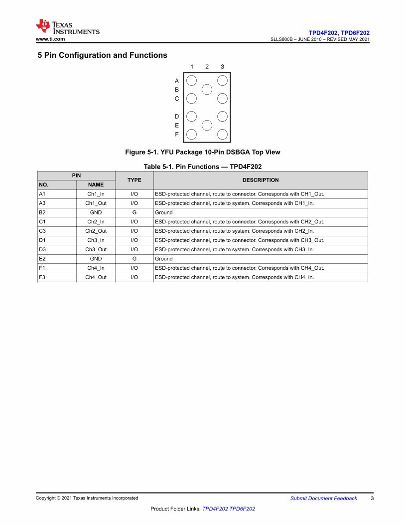
5 Pin Configuration and Functions
Figure 5-1. YFU Package 10-Pin DSBGA Top View
Table 5-1. Pin Functions — TPD4F202PIN
TYPE DESCRIPTIONNO. NAMEA1 Ch1_In I/O ESD-protected channel, route to connector. Corresponds with CH1_Out.
A3 Ch1_Out I/O ESD-protected channel, route to system. Corresponds with CH1_In.
B2 GND G Ground
C1 Ch2_In I/O ESD-protected channel, route to connector. Corresponds with CH2_Out.
C3 Ch2_Out I/O ESD-protected channel, route to system. Corresponds with CH2_In.
D1 Ch3_In I/O ESD-protected channel, route to connector. Corresponds with CH3_Out.
D3 Ch3_Out I/O ESD-protected channel, route to system. Corresponds with CH3_In.
E2 GND G Ground
F1 Ch4_In I/O ESD-protected channel, route to connector. Corresponds with CH4_Out.
F3 Ch4_Out I/O ESD-protected channel, route to system. Corresponds with CH4_In.
www.ti.comTPD4F202, TPD6F202
SLLS800B – JUNE 2010 – REVISED MAY 2021
Copyright © 2021 Texas Instruments Incorporated Submit Document Feedback 3
Product Folder Links: TPD4F202 TPD6F202

Figure 5-2. YFU Package 15-Pin DSBGA Top View
Table 5-2. Pin Functions — TPD6F202PIN
TYPE DESCRIPTIONNO. NAMEA1 Ch1_In I/O ESD-protected channel, route to connector. Corresponds with CH1_Out.
A3 Ch1_Out I/O ESD-protected channel, route to system. Corresponds with CH1_In.
B2 GND G Ground
C1 Ch2_In I/O ESD-protected channel, route to connector. Corresponds with CH2_Out.
C3 Ch2_Out I/O ESD-protected channel, route to system. Corresponds with CH2_In.
D1 Ch3_In I/O ESD-protected channel, route to connector. Corresponds with CH3_Out.
D3 Ch3_Out I/O ESD-protected channel, route to system. Corresponds with CH3_In.
E2 GND G Ground
F1 Ch4_In I/O ESD-protected channel, route to connector. Corresponds with CH4_Out.
F3 Ch4_Out I/O ESD-protected channel, route to system. Corresponds with CH4_In.
G1 Ch5_In I/O ESD-protected channel, route to connector. Corresponds with CH5_Out.
G3 Ch5_Out I/O ESD-protected channel, route to system. Corresponds with CH5_In.
H2 GND G Ground
J1 Ch6_In I/O ESD-protected channel, route to connector. Corresponds with CH6_Out.
J3 Ch6_Out I/O ESD-protected channel, route to system. Corresponds with CH6_In.
TPD4F202, TPD6F202SLLS800B – JUNE 2010 – REVISED MAY 2021 www.ti.com
4 Submit Document Feedback Copyright © 2021 Texas Instruments Incorporated
Product Folder Links: TPD4F202 TPD6F202

6 Specifications6.1 Absolute Maximum Ratingsover operating free-air temperature range (unless otherwise noted)(1)
MIN MAX UNITVIO IO to GND –0.3 6 V
Continuous power dissipation (TA = 70°C) 100 mW
TJ Junction temperature 150 °C
Lead temperature (soldering, 10 s) 300 °C
Tstg Storage temperature –65 150 °C
(1) Stresses beyond those listed under Absolute Maximum Ratings may cause permanent damage to the device. These are stressratings only, which do not imply functional operation of the device at these or any other conditions beyond those indicated underRecommended Operating Conditions. Exposure to absolute-maximum-rated conditions for extended periods may affect devicereliability.
6.2 ESD Ratings — JEDECVALUE UNIT
V(ESD)Electrostaticdischarge
Human-body model (HBM), per ANSI/ESDA/JEDEC JS-001(1) ±15000V
Charged-device model (CDM), per JEDEC specification JESD22-C101(2) ±1500
(1) JEDEC document JEP155 states that 500-V HBM allows safe manufacturing with a standard ESD control process.(2) JEDEC document JEP157 states that 250-V CDM allows safe manufacturing with a standard ESD control process.
6.3 ESD Ratings — IECVALUE UNIT
V(ESD)Electrostaticdischarge
IEC 61000-4-2 contact discharge ±25000V
IEC 61000-4-2 air-gap discharge ±25000
6.4 Recommended Operating Conditionsover operating free-air temperature range (unless otherwise noted)
MIN MAX UNITVIO I/O to GND 0 5.5 V
TA Ambient temperature –40 85 °C
6.5 Thermal Information
THERMAL METRIC(1)
TPD4F202 TPD6F202UNITYFU (DSBGA) YFU (DSBGA)
10 PINS 15 PINSRθJA Junction-to-ambient thermal resistance 91.8 72 °C/W
RθJC(top) Junction-to-case (top) thermal resistance 1 0.6 °C/W
RθJB Junction-to-board thermal resistance 19.7 14.1 °C/W
ψJT Junction-to-top characterization parameter 0.5 0.3 °C/W
ψJB Junction-to-board characterization parameter 19.7 14.1 °C/W
RθJC(bot) Junction-to-case (bottom) thermal resistance n/a n/a °C/W
(1) For more information about traditional and new thermal metrics, see the Semiconductor and IC Package Thermal Metrics applicationreport, SPRA953.
www.ti.comTPD4F202, TPD6F202
SLLS800B – JUNE 2010 – REVISED MAY 2021
Copyright © 2021 Texas Instruments Incorporated Submit Document Feedback 5
Product Folder Links: TPD4F202 TPD6F202

6.6 Electrical CharacteristicsTA = –40°C to 85°C (Unless otherwise noted)
PARAMETER TEST CONDITIONS MIN TYP(1) MAX UNIT
VBR DC breakdown voltage IIO = 10 μA 6 V
R Resistance 85 100 115 Ω
C Capacitance (C1 or C2) VIO = 3.3 V, ƒ = 1 MHz 15 pF
IIO Channel leakage current VIO = 3.3 V 10 nA
fC Cut-off frequency ZSOURCE = 50 Ω, ZLOAD = 50 Ω 108 MHz
(1) Typical values are at TA = 25°C.
TPD4F202, TPD6F202SLLS800B – JUNE 2010 – REVISED MAY 2021 www.ti.com
6 Submit Document Feedback Copyright © 2021 Texas Instruments Incorporated
Product Folder Links: TPD4F202 TPD6F202

6.7 Typical Characteristics
Figure 6-1. Channel-to-Channel Crosstalk Figure 6-2. Frequency Response Data (0-V Bias)
Time (nS)
Am
plit
ud
e (
V)
0 25 50 75 100 125 150 175 200 225 250-5
0
5
10
15
20
25
30
35
40
45
50Out Pin (ESD Strike Terminal)Input Pin (Internal Terminal)
Figure 6-3. IEC Clamping Waveforms +8-kVContact
Time (nS)
Am
plit
ud
e (
V)
0 25 50 75 100 125 150 175 200 225 250-50
-45
-40
-35
-30
-25
-20
-15
-10
-5
0
5
Out Pin (ESD Strike Terminal)Input Pin (Internal Terminal)
Figure 6-4. IEC Clamping Waveforms –8-kVContact
Figure 6-5. DC Characteristics (IIN vs VIN), TA =25°C
Figure 6-6. C1 or C2 Capacitance vs VBIAS
www.ti.comTPD4F202, TPD6F202
SLLS800B – JUNE 2010 – REVISED MAY 2021
Copyright © 2021 Texas Instruments Incorporated Submit Document Feedback 7
Product Folder Links: TPD4F202 TPD6F202
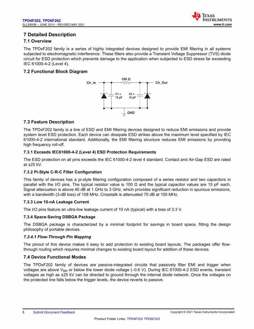
7 Detailed Description7.1 OverviewThe TPDxF202 family is a series of highly integrated devices designed to provide EMI filtering in all systemssubjected to electromagnetic interference. These filters also provide a Transient Voltage Suppressor (TVS) diodecircuit for ESD protection which prevents damage to the application when subjected to ESD stress far exceedingIEC 61000-4-2 (Level 4).
7.2 Functional Block Diagram
7.3 Feature DescriptionThe TPDxF202 family is a line of ESD and EMI filtering devices designed to reduce EMI emissions and providesystem level ESD protection. Each device can dissipate ESD strikes above the maximum level specified by IEC61000-4-2 international standard. Additionally, the EMI filtering structure reduces EMI emissions by providinghigh frequency roll-off.
7.3.1 Exceeds IEC61000-4-2 (Level 4) ESD Protection Requirements
The ESD protection on all pins exceeds the IEC 61000-4-2 level 4 standard. Contact and Air-Gap ESD are ratedat ±25 kV.
7.3.2 Pi-Style C-R-C Filter Configuration
This family of devices has a pi-style filtering configuration composed of a series resistor and two capacitors inparallel with the I/O pins. The typical resistor value is 100 Ω and the typical capacitor values are 15 pF each.Signal attenuation is above 40 dB at 1 GHz to 3 GHz, which provides significant reduction in spurious emissions,with a bandwidth (3-dB loss) of 108 MHz. Crosstalk is attenuated 70 dB at 100 MHz.
7.3.3 Low 10-nA Leakage Current
The I/O pins feature an ultra-low leakage current of 10 nA (typical) with a bias of 3.3 V.
7.3.4 Space-Saving DSBGA Package
The DSBGA package is characterized by a minimal footprint for savings in board space, fitting the designphilosophy of portable devices.
7.3.4.1 Flow-Through Pin Mapping
The pinout of this device makes it easy to add protection to existing board layouts. The packages offer flow-through routing which requires minimal changes to existing board layout for addition of these devices.
7.4 Device Functional ModesThe TPDxF202 family of devices are passive-integrated circuits that passively filter EMI and trigger whenvoltages are above VBR or below the lower diode voltage (–0.6 V). During IEC 61000-4-2 ESD events, transientvoltages as high as ±25 kV can be directed to ground through the internal diode network. Once the voltages onthe protected line falls below the trigger levels, the device reverts to passive.
TPD4F202, TPD6F202SLLS800B – JUNE 2010 – REVISED MAY 2021 www.ti.com
8 Submit Document Feedback Copyright © 2021 Texas Instruments Incorporated
Product Folder Links: TPD4F202 TPD6F202

8 Application and ImplementationNote
Information in the following applications sections is not part of the TI component specification,and TI does not warrant its accuracy or completeness. TI’s customers are responsible fordetermining suitability of components for their purposes, as well as validating and testing their designimplementation to confirm system functionality.
8.1 Application Information
The TPDxF202 family are diode-type TVSs integrated with series resistors and parallel capacitors for filteringemitted EMI. As a signal passes through the device, higher frequency components are filtered out. This devicealso provides a path to ground during ESD events and isolates the protected IC. As the current from ESDpasses through the TVS, only a small voltage drop is present across the diode. This is the voltage presentedto the protected IC. In particular, these filters are ideal for EMI filtering and protecting data lines from ESD atdisplay, keypad, and memory interfaces.
8.2 Typical Application
GND
TPD6F202GND
TPD6F202GND
TPD6F202
Co
nn
ecto
r
Dis
pla
y P
an
el C
on
ne
cto
r
R0
R1
R2
R3
R4
R5
G0
G1
G2
G3
G4
G5
B0
B1
B2
B3
B4
B5
A1
C1
D1
F1
G1
J1 J3
G3
A3
C3
D3
F3
A1
C1
D1
F1
G1
J1 J3
G3
A3
C3
D3
F3
A1
C1
D1
F1
G1
J1 J3
G3
A3
C3
D3
F3
B2
E2
H2
B2
E2
H2
B2
E2
H2
Figure 8-1. Display Panel Schematic
www.ti.comTPD4F202, TPD6F202
SLLS800B – JUNE 2010 – REVISED MAY 2021
Copyright © 2021 Texas Instruments Incorporated Submit Document Feedback 9
Product Folder Links: TPD4F202 TPD6F202

8.2.1 Design Requirements
For this design example, three TPD6F202 devices are used in an 18-bit display panel application. Thisapplication provides a complete ESD and EMI protection solution for the display connector. For the displaypanel application, the following parameters are in shown Table 8-1.
Table 8-1. Design ParametersDESIGN PARAMETER VALUE
Signal range on all pins except GND 0 V to 5 V
Data Rate 200 Mbps
ESD Protection Level IEC 61000-4-2 Level 4
8.2.2 Detailed Design Procedure
To begin the design process, some design parameters must be decided; the designer needs to know theoperating frequency and the signal range on all the protected lines.
8.2.2.1 Signal Range on All Protected Lines
The TPD6F202 has 6 identical protection channels for signal lines. All I/O pins will support a signal range from 0to 5.5 V.
8.2.2.2 Data Rate
The TPD6F202 has a 108-MHz, –3-dB bandwidth, which supports the data rate for this display.
8.2.2.3 ESD Protection Level
The contact and air-gap ratings of ± 25 kV for TPD6F202 exceeds the IEC 61000-4-2 Level 4 rating of ± 8-kVcontact and ± 15-kV air-gap ratings.
8.2.3 Application Curve
Figure 8-2. Frequency Response Data (0-V Bias)
9 Power Supply RecommendationsThe TPDxF202 device is a passive ESD-protection device, and therefore, does not require a power supply. Takecare to avoid violating the maximum-voltage specification to ensure that the device functions properly. The IOlines can tolerate up to 6-V DC.
TPD4F202, TPD6F202SLLS800B – JUNE 2010 – REVISED MAY 2021 www.ti.com
10 Submit Document Feedback Copyright © 2021 Texas Instruments Incorporated
Product Folder Links: TPD4F202 TPD6F202

10 Layout10.1 Layout GuidelinesTypically, there are multiple EMI filters being used in portable applications to suppress the EMI interference.This means the total board area consumed by EMI filters are relatively large. One example of space-savinginnovation is to place the EMI filters right under the connectors so that the main PCB space is not used. TheYFU packages of the TPDxF202 series offer ultra low-profile package height which enables such innovativecomponent placement in portable applications. Package under-fill is recommended while using the YFUpackages in flex boards.
• The optimum placement is as close to the connector as possible.– EMI during an ESD event can couple from the trace being struck to other nearby unprotected traces,
resulting in early system failures.– The PCB designer needs to minimize the possibility of EMI coupling by keeping any unprotected traces
away from the protected traces which are between the TVS and the connector.• Route the protected traces as straight as possible.• Eliminate any sharp corners on the protected traces between the TVS and the connector by using rounded
corners with the largest radii possible.– Electric fields tend to build up on corners, increasing EMI coupling.
For maximum efficiency of filtering and ESD protection, while doing the board layout, take care to reduce boardparasitic series inductances from package GND pins to board GND plane. The TPDxF202 devices must beconnected to a ground plane with a micro via adjacent to the device GND pad. If this is not possible, theconnection to the ground plane must be as direct as possible to minimize the inductance. Due to flow-throughpin mapping, the signal pins routing is easily achieved in a single layer.
10.2 Layout Example
A1
B2
C1
D1
F1
E2
F3
D3
C3
A3 A1
B2
C1
D1
F1
E2
F3
D3
C3
A3
G1
J1
H2
J3
G3Legend
VIA to Ground Plane
TPD4F202 TPD6F202
PCB Trace
Figure 10-1. Board Layout With TPDxF202
www.ti.comTPD4F202, TPD6F202
SLLS800B – JUNE 2010 – REVISED MAY 2021
Copyright © 2021 Texas Instruments Incorporated Submit Document Feedback 11
Product Folder Links: TPD4F202 TPD6F202

11 Device and Documentation Support11.1 Documentation Support11.1.1 Related Documentation
The following documents contain additional information related to the use of the TPDxF202 device:
• Texas Instruments, ESD Protection Layout Guide application report• Texas Intruments, Reading and Understanding an ESD Protection Data Sheet application report
11.2 Related LinksThe table below lists quick access links. Categories include technical documents, support and communityresources, tools and software, and quick access to sample or buy.
Table 11-1. Related LinksPARTS PRODUCT FOLDER SAMPLE & BUY TECHNICAL
DOCUMENTSTOOLS &
SOFTWARESUPPORT &COMMUNITY
TPD4F202 Click here Click here Click here Click here Click here
TPD6F202 Click here Click here Click here Click here Click here
11.3 Support ResourcesTI E2E™ support forums are an engineer's go-to source for fast, verified answers and design help — straightfrom the experts. Search existing answers or ask your own question to get the quick design help you need.
Linked content is provided "AS IS" by the respective contributors. They do not constitute TI specifications and donot necessarily reflect TI's views; see TI's Terms of Use.
11.4 TrademarksTI E2E™ is a trademark of Texas Instruments.All trademarks are the property of their respective owners.11.5 Electrostatic Discharge Caution
This integrated circuit can be damaged by ESD. Texas Instruments recommends that all integrated circuits be handledwith appropriate precautions. Failure to observe proper handling and installation procedures can cause damage.ESD damage can range from subtle performance degradation to complete device failure. Precision integrated circuits maybe more susceptible to damage because very small parametric changes could cause the device not to meet its publishedspecifications.
11.6 GlossaryTI Glossary This glossary lists and explains terms, acronyms, and definitions.
12 Mechanical, Packaging, and Orderable InformationThe following pages include mechanical, packaging, and orderable information. This information is the mostcurrent data available for the designated devices. This data is subject to change without notice and revision ofthis document. For browser-based versions of this data sheet, refer to the left-hand navigation.
TPD4F202, TPD6F202SLLS800B – JUNE 2010 – REVISED MAY 2021 www.ti.com
12 Submit Document Feedback Copyright © 2021 Texas Instruments Incorporated
Product Folder Links: TPD4F202 TPD6F202

PACKAGE OPTION ADDENDUM
www.ti.com 13-May-2021
Addendum-Page 1
PACKAGING INFORMATION
Orderable Device Status(1)
Package Type PackageDrawing
Pins PackageQty
Eco Plan(2)
Lead finish/Ball material
(6)
MSL Peak Temp(3)
Op Temp (°C) Device Marking(4/5)
Samples
TPD4F202YFUR ACTIVE DSBGA YFU 10 3000 RoHS & Green SNAGCU Level-1-260C-UNLIM -40 to 85 57S
TPD6F202YFUR ACTIVE DSBGA YFU 15 3000 RoHS & Green SNAGCU Level-1-260C-UNLIM -40 to 85 5WS
(1) The marketing status values are defined as follows:ACTIVE: Product device recommended for new designs.LIFEBUY: TI has announced that the device will be discontinued, and a lifetime-buy period is in effect.NRND: Not recommended for new designs. Device is in production to support existing customers, but TI does not recommend using this part in a new design.PREVIEW: Device has been announced but is not in production. Samples may or may not be available.OBSOLETE: TI has discontinued the production of the device.
(2) RoHS: TI defines "RoHS" to mean semiconductor products that are compliant with the current EU RoHS requirements for all 10 RoHS substances, including the requirement that RoHS substancedo not exceed 0.1% by weight in homogeneous materials. Where designed to be soldered at high temperatures, "RoHS" products are suitable for use in specified lead-free processes. TI mayreference these types of products as "Pb-Free".RoHS Exempt: TI defines "RoHS Exempt" to mean products that contain lead but are compliant with EU RoHS pursuant to a specific EU RoHS exemption.Green: TI defines "Green" to mean the content of Chlorine (Cl) and Bromine (Br) based flame retardants meet JS709B low halogen requirements of <=1000ppm threshold. Antimony trioxide basedflame retardants must also meet the <=1000ppm threshold requirement.
(3) MSL, Peak Temp. - The Moisture Sensitivity Level rating according to the JEDEC industry standard classifications, and peak solder temperature.
(4) There may be additional marking, which relates to the logo, the lot trace code information, or the environmental category on the device.
(5) Multiple Device Markings will be inside parentheses. Only one Device Marking contained in parentheses and separated by a "~" will appear on a device. If a line is indented then it is a continuationof the previous line and the two combined represent the entire Device Marking for that device.
(6) Lead finish/Ball material - Orderable Devices may have multiple material finish options. Finish options are separated by a vertical ruled line. Lead finish/Ball material values may wrap to twolines if the finish value exceeds the maximum column width.
Important Information and Disclaimer:The information provided on this page represents TI's knowledge and belief as of the date that it is provided. TI bases its knowledge and belief on informationprovided by third parties, and makes no representation or warranty as to the accuracy of such information. Efforts are underway to better integrate information from third parties. TI has taken andcontinues to take reasonable steps to provide representative and accurate information but may not have conducted destructive testing or chemical analysis on incoming materials and chemicals.TI and TI suppliers consider certain information to be proprietary, and thus CAS numbers and other limited information may not be available for release.
In no event shall TI's liability arising out of such information exceed the total purchase price of the TI part(s) at issue in this document sold by TI to Customer on an annual basis.

PACKAGE OPTION ADDENDUM
www.ti.com 13-May-2021
Addendum-Page 2

TAPE AND REEL INFORMATION
*All dimensions are nominal
Device PackageType
PackageDrawing
Pins SPQ ReelDiameter
(mm)
ReelWidth
W1 (mm)
A0(mm)
B0(mm)
K0(mm)
P1(mm)
W(mm)
Pin1Quadrant
TPD4F202YFUR DSBGA YFU 10 3000 178.0 9.2 1.21 1.72 0.45 4.0 8.0 Q1
TPD6F202YFUR DSBGA YFU 15 3000 178.0 9.2 1.19 2.5 0.45 4.0 8.0 Q1
PACKAGE MATERIALS INFORMATION
www.ti.com 13-May-2021
Pack Materials-Page 1

*All dimensions are nominal
Device Package Type Package Drawing Pins SPQ Length (mm) Width (mm) Height (mm)
TPD4F202YFUR DSBGA YFU 10 3000 220.0 220.0 35.0
TPD6F202YFUR DSBGA YFU 15 3000 220.0 220.0 35.0
PACKAGE MATERIALS INFORMATION
www.ti.com 13-May-2021
Pack Materials-Page 2

D: Max =
E: Max =
2.31 mm, Min =
1.003 mm, Min =
2.25 mm
0.942 mm

IMPORTANT NOTICE AND DISCLAIMERTI PROVIDES TECHNICAL AND RELIABILITY DATA (INCLUDING DATASHEETS), DESIGN RESOURCES (INCLUDING REFERENCEDESIGNS), APPLICATION OR OTHER DESIGN ADVICE, WEB TOOLS, SAFETY INFORMATION, AND OTHER RESOURCES “AS IS”AND WITH ALL FAULTS, AND DISCLAIMS ALL WARRANTIES, EXPRESS AND IMPLIED, INCLUDING WITHOUT LIMITATION ANYIMPLIED WARRANTIES OF MERCHANTABILITY, FITNESS FOR A PARTICULAR PURPOSE OR NON-INFRINGEMENT OF THIRDPARTY INTELLECTUAL PROPERTY RIGHTS.These resources are intended for skilled developers designing with TI products. You are solely responsible for (1) selecting the appropriateTI products for your application, (2) designing, validating and testing your application, and (3) ensuring your application meets applicablestandards, and any other safety, security, or other requirements. These resources are subject to change without notice. TI grants youpermission to use these resources only for development of an application that uses the TI products described in the resource. Otherreproduction and display of these resources is prohibited. No license is granted to any other TI intellectual property right or to any third partyintellectual property right. TI disclaims responsibility for, and you will fully indemnify TI and its representatives against, any claims, damages,costs, losses, and liabilities arising out of your use of these resources.TI’s products are provided subject to TI’s Terms of Sale (https:www.ti.com/legal/termsofsale.html) or other applicable terms available eitheron ti.com or provided in conjunction with such TI products. TI’s provision of these resources does not expand or otherwise alter TI’sapplicable warranties or warranty disclaimers for TI products.IMPORTANT NOTICE
Mailing Address: Texas Instruments, Post Office Box 655303, Dallas, Texas 75265Copyright © 2021, Texas Instruments Incorporated