Embed Size (px)
Citation preview
VIN
POWER MANAGEMENT
VOUT
GND
µC
GPIO
VDD
GND
TPL5110
VDD
GND
EN/ONE_SHOT
DRV
DELAY/M_DRV
DONE
REXT
Battery
-+
Product
Folder
Sample &Buy
Technical
Documents
Tools &
Software
Support &Community
An IMPORTANT NOTICE at the end of this data sheet addresses availability, warranty, changes, use in safety-critical applications,intellectual property matters and other important disclaimers. PRODUCTION DATA.
TPL5110SNAS650 –JANUARY 2015–REVISED JANUARY 2015
TPL5110 Nano-power System Timer for Power Gating
1
1 Features1• Supply Voltage from 1.8V to 5.5V• Current Consumption at 2.5V 35nA (typ)• Selectable Time Intervals 100ms to 7200s• Timer Accuracy 1% (typ)• Resistor Selectable Time Interval• Manual MOSFET Power On• One-shot Feature
2 Applications• Battery Powered Systems• Internet of Things (IoT)• Intruder Detection• Tamper Detection• Home Automation Sensors• Thermostats• Consumer Electronics• Remote Sensor• White Goods
3 DescriptionThe TPL5110 Nano Timer is a low power timer withan integrated MOSFET driver ideal for power gatingin duty cycled or battery powered applications.Consuming only 35nA, the TPL5110 can enable thepower supply line and drastically reduce the overallsystem stand by current during the sleep time. Suchpower savings enable the use of significantly smallerbatteries making it well suited for energy harvestingor wireless sensor applications. The TPL5110provides selectable timing intervals from 100ms to7200s and is designed for power gating applications.In addition, the TPL5110 has a unique One-shotfeature where the timer will only power the MOSFETfor one cycle. The TPL5110 is available in a 6-pinSOT23 package.
Device Information(1)
PART NUMBER PACKAGE BODY SIZE (NOM)TPL5110 SOT23 (6) 3.00 mm x 3.00 mm
(1) For all available packages, see the orderable addendum atthe end of the datasheet.
4 Simplified Application Schematic
2
TPL5110SNAS650 –JANUARY 2015–REVISED JANUARY 2015 www.ti.com
Product Folder Links: TPL5110
Submit Documentation Feedback Copyright © 2015, Texas Instruments Incorporated
Table of Contents1 Features .................................................................. 12 Applications ........................................................... 13 Description ............................................................. 14 Simplified Application Schematic ........................ 15 Revision History..................................................... 26 Pin Configuration and Functions ......................... 37 Specifications......................................................... 4
7.1 Absolute Maximum Ratings ...................................... 47.2 ESD Ratings ............................................................ 47.3 Recommended Operating Ratings ........................... 47.4 Thermal Information ................................................. 47.5 Electrical Characteristics........................................... 57.6 Timing Requirements ............................................... 67.7 Typical Characteristics .............................................. 7
8 Detailed Description .............................................. 88.1 Overview ................................................................... 8
8.2 Functional Block Diagram ......................................... 88.3 Feature Description................................................... 88.4 Device Functional Modes.......................................... 98.5 Programming .......................................................... 10
9 Application and Implementation ........................ 169.1 Application Information............................................ 169.2 Typical Application ................................................. 16
10 Power Supply Recommendations ..................... 1711 Layout................................................................... 17
11.1 Layout Guidelines ................................................. 1711.2 Layout Example .................................................... 18
12 Device and Documentation Support ................. 1912.1 Trademarks ........................................................... 1912.2 Electrostatic Discharge Caution............................ 1912.3 Glossary ................................................................ 19
13 Mechanical, Packaging, and OrderableInformation ........................................................... 19
5 Revision History
DATE REVISION NOTESJanuary 2015 * Initial release.
TPL5110
VDD
GND
EN/ONE_ SHOT
DRV
DELAY/M_DRV
DONE
1
2
3 4
5
6
3
TPL5110www.ti.com SNAS650 –JANUARY 2015–REVISED JANUARY 2015
Product Folder Links: TPL5110
Submit Documentation FeedbackCopyright © 2015, Texas Instruments Incorporated
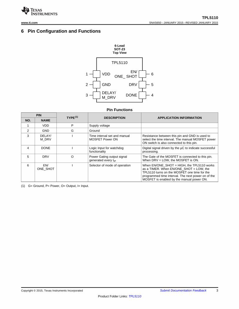
(1) G= Ground, P= Power, O= Output, I= Input.
6 Pin Configuration and Functions
6-LeadSOT-23
Top View
Pin FunctionsPIN
TYPE (1) DESCRIPTION APPLICATION INFORMATIONNO. NAME
1 VDD P Supply voltage2 GND G Ground3 DELAY/
M_DRVI Time interval set and manual
MOSFET Power ONResistance between this pin and GND is used toselect the time interval. The manual MOSFET powerON switch is also connected to this pin.
4 DONE I Logic Input for watchdogfunctionality
Digital signal driven by the µC to indicate successfulprocessing.
5 DRV O Power Gating output signalgenerated every tIP
The Gate of the MOSFET is connected to this pin.When DRV = LOW, the MOSFET is ON.
6 EN/ONE_SHOT
I Selector of mode of operation When EN/ONE_SHOT = HIGH, the TPL5110 worksas a TIMER. When EN/ONE_SHOT = LOW, theTPL5110 turns on the MOSFET one time for theprogrammed time interval. The next power on of theMOSFET is enabled by the manual power ON.
4
TPL5110SNAS650 –JANUARY 2015–REVISED JANUARY 2015 www.ti.com
Product Folder Links: TPL5110
Submit Documentation Feedback Copyright © 2015, Texas Instruments Incorporated
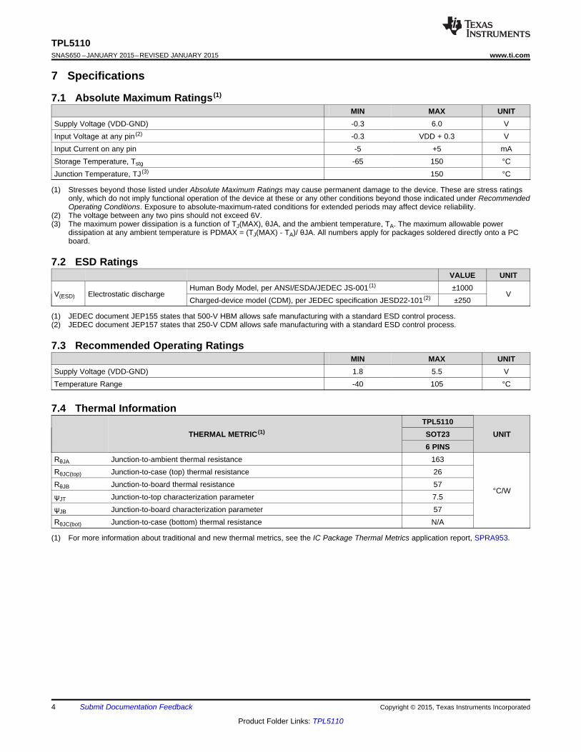
(1) Stresses beyond those listed under Absolute Maximum Ratings may cause permanent damage to the device. These are stress ratingsonly, which do not imply functional operation of the device at these or any other conditions beyond those indicated under RecommendedOperating Conditions. Exposure to absolute-maximum-rated conditions for extended periods may affect device reliability.
(2) The voltage between any two pins should not exceed 6V.(3) The maximum power dissipation is a function of TJ(MAX), θJA, and the ambient temperature, TA. The maximum allowable power
dissipation at any ambient temperature is PDMAX = (TJ(MAX) - TA)/ θJA. All numbers apply for packages soldered directly onto a PCboard.
7 Specifications
7.1 Absolute Maximum Ratings (1)
MIN MAX UNITSupply Voltage (VDD-GND) -0.3 6.0 VInput Voltage at any pin (2) -0.3 VDD + 0.3 VInput Current on any pin -5 +5 mAStorage Temperature, Tstg -65 150 °CJunction Temperature, TJ (3) 150 °C
(1) JEDEC document JEP155 states that 500-V HBM allows safe manufacturing with a standard ESD control process.(2) JEDEC document JEP157 states that 250-V CDM allows safe manufacturing with a standard ESD control process.
7.2 ESD RatingsVALUE UNIT
V(ESD) Electrostatic dischargeHuman Body Model, per ANSI/ESDA/JEDEC JS-001 (1) ±1000
VCharged-device model (CDM), per JEDEC specification JESD22-101 (2) ±250
7.3 Recommended Operating RatingsMIN MAX UNIT
Supply Voltage (VDD-GND) 1.8 5.5 VTemperature Range -40 105 °C
(1) For more information about traditional and new thermal metrics, see the IC Package Thermal Metrics application report, SPRA953.
7.4 Thermal Information
THERMAL METRIC (1)TPL5110
UNITSOT236 PINS
RθJA Junction-to-ambient thermal resistance 163
°C/W
RθJC(top) Junction-to-case (top) thermal resistance 26RθJB Junction-to-board thermal resistance 57ψJT Junction-to-top characterization parameter 7.5ψJB Junction-to-board characterization parameter 57RθJC(bot) Junction-to-case (bottom) thermal resistance N/A
5
TPL5110www.ti.com SNAS650 –JANUARY 2015–REVISED JANUARY 2015
Product Folder Links: TPL5110
Submit Documentation FeedbackCopyright © 2015, Texas Instruments Incorporated
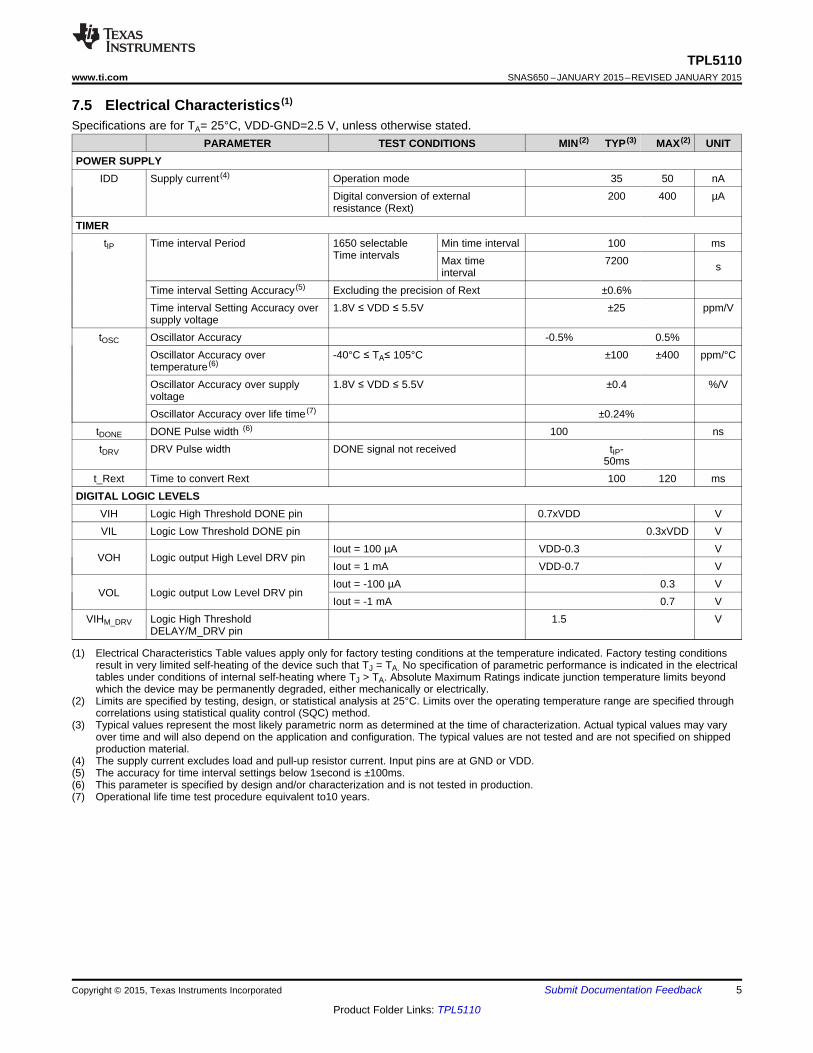
(1) Electrical Characteristics Table values apply only for factory testing conditions at the temperature indicated. Factory testing conditionsresult in very limited self-heating of the device such that TJ = TA. No specification of parametric performance is indicated in the electricaltables under conditions of internal self-heating where TJ > TA. Absolute Maximum Ratings indicate junction temperature limits beyondwhich the device may be permanently degraded, either mechanically or electrically.
(2) Limits are specified by testing, design, or statistical analysis at 25°C. Limits over the operating temperature range are specified throughcorrelations using statistical quality control (SQC) method.
(3) Typical values represent the most likely parametric norm as determined at the time of characterization. Actual typical values may varyover time and will also depend on the application and configuration. The typical values are not tested and are not specified on shippedproduction material.
(4) The supply current excludes load and pull-up resistor current. Input pins are at GND or VDD.(5) The accuracy for time interval settings below 1second is ±100ms.(6) This parameter is specified by design and/or characterization and is not tested in production.(7) Operational life time test procedure equivalent to10 years.
7.5 Electrical Characteristics (1)
Specifications are for TA= 25°C, VDD-GND=2.5 V, unless otherwise stated.PARAMETER TEST CONDITIONS MIN (2) TYP (3) MAX (2) UNIT
POWER SUPPLYIDD Supply current (4) Operation mode 35 50 nA
Digital conversion of externalresistance (Rext)
200 400 µA
TIMERtIP Time interval Period 1650 selectable
Time intervalsMin time interval 100 msMax timeinterval
7200 s
Time interval Setting Accuracy (5) Excluding the precision of Rext ±0.6%Time interval Setting Accuracy oversupply voltage
1.8V ≤ VDD ≤ 5.5V ±25 ppm/V
tOSC Oscillator Accuracy -0.5% 0.5%Oscillator Accuracy overtemperature (6)
-40°C ≤ TA≤ 105°C ±100 ±400 ppm/°C
Oscillator Accuracy over supplyvoltage
1.8V ≤ VDD ≤ 5.5V ±0.4 %/V
Oscillator Accuracy over life time (7) ±0.24%tDONE DONE Pulse width (6) 100 nstDRV DRV Pulse width DONE signal not received tIP-
50mst_Rext Time to convert Rext 100 120 ms
DIGITAL LOGIC LEVELSVIH Logic High Threshold DONE pin 0.7xVDD VVIL Logic Low Threshold DONE pin 0.3xVDD V
VOH Logic output High Level DRV pinIout = 100 µA VDD-0.3 VIout = 1 mA VDD-0.7 V
VOL Logic output Low Level DRV pinIout = -100 µA 0.3 VIout = -1 mA 0.7 V
VIHM_DRV Logic High ThresholdDELAY/M_DRV pin
1.5 V
EN/ONE_SHOT
VDD
DONE
DRV
t tIPt
ttDDONEt tDONE
trDRV
tfDRV
DELAY/M_DRV
ttM_DRV
tR_EXT
t tIPt
t tDRVt t tDRV + tDBt
6
TPL5110SNAS650 –JANUARY 2015–REVISED JANUARY 2015 www.ti.com
Product Folder Links: TPL5110
Submit Documentation Feedback Copyright © 2015, Texas Instruments Incorporated
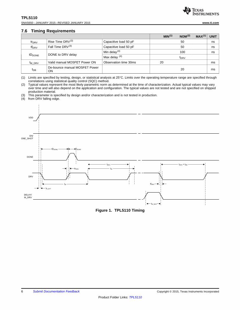
(1) Limits are specified by testing, design, or statistical analysis at 25°C. Limits over the operating temperature range are specified throughcorrelations using statistical quality control (SQC) method.
(2) Typical values represent the most likely parametric norm as determined at the time of characterization. Actual typical values may varyover time and will also depend on the application and configuration. The typical values are not tested and are not specified on shippedproduction material.
(3) This parameter is specified by design and/or characterization and is not tested in production.(4) from DRV falling edge.
7.6 Timing RequirementsMIN (1) NOM (2) MAX (1) UNIT
trDRV Rise Time DRV (3) Capacitive load 50 pF 50 nstfDRV Fall Time DRV (3) Capacitive load 50 pF 50 ns
tDDONE DONE to DRV delayMin delay (4) 100 nsMax delay (4) tDRV
tM_DRV Valid manual MOSFET Power ON Observation time 30ms 20 ms
tDBDe-bounce manual MOSFET PowerON 20 ms
Figure 1. TPL5110 Timing
Accuracy (%)
Fre
qu
ency
0
5%
10%
15%
20%
25%
30%
35%
40%
-1 -0.8 -0.6 -0.4 -0.2 0 0.2 0.4 0.6 0.8Time (s)
Su
pp
ly c
urr
ent
(PA
)
0 0.1 0.2 0.3 0.4 0.5 0.6 0.7 0.8 0.9 10.01
0.1
1
10
100
1000
PORREXT READING
TIMER MODE
Supply Voltage (V)
Osc
illat
or
accu
racy
(%
)
1.5 1.9 2.3 2.7 3.1 3.5 3.9 4.3 4.7 5.1 5.5-1
-0.5
0
0.5
1
1.5
2TA= -40°CTA= 25°CTA= 70°CTA= 105°C
Temperature (°C)
Osc
illat
or a
ccur
acy
(%)
-40 -25 -10 5 20 35 50 65 80 95 110-1
-0.5
0
0.5
1
1.5
2VDD= 1.8VVDD= 2.5VVDD= 3.3VVDD= 5.5V
Supply Voltage (V)
Su
pp
ly c
urr
ent
(nA
)
1.5 1.9 2.3 2.7 3.1 3.5 3.9 4.3 4.7 5.1 5.520
30
40
50
60
70
80TA= -40°CTA= 25°CTA= 70°CTA= 105°C
Temperature (°C)
Sup
ply
curr
ent (
nA)
-40 -25 -10 5 20 35 50 65 80 95 11020
30
40
50
60
70
80VDD= 1.8VVDD= 2.5VVDD= 3.3VVDD= 5.5V
7
TPL5110www.ti.com SNAS650 –JANUARY 2015–REVISED JANUARY 2015
Product Folder Links: TPL5110
Submit Documentation FeedbackCopyright © 2015, Texas Instruments Incorporated
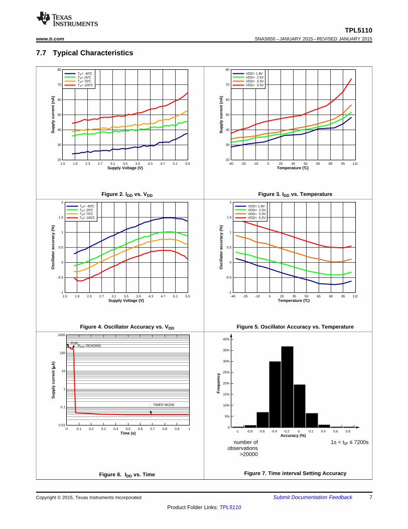
7.7 Typical Characteristics
Figure 2. IDD vs. VDD Figure 3. IDD vs. Temperature
Figure 4. Oscillator Accuracy vs. VDD Figure 5. Oscillator Accuracy vs. Temperature
Figure 6. IDD vs. Time
number ofobservations
>20000
1s < tIP ≤ 7200s
Figure 7. Time interval Setting Accuracy
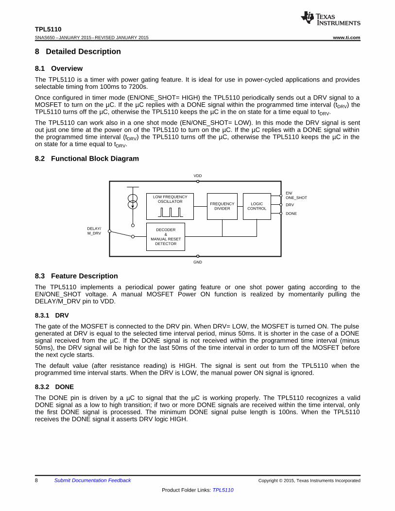
LOW FREQUENCY OSCILLATOR
FREQUENCY DIVIDER
EN/ONE_SHOT
DRV
VDD
GND
DELAY/M_DRV
DECODER&
MANUAL RESETDETECTOR
LOGICCONTROL
DONE
8
TPL5110SNAS650 –JANUARY 2015–REVISED JANUARY 2015 www.ti.com
Product Folder Links: TPL5110
Submit Documentation Feedback Copyright © 2015, Texas Instruments Incorporated
8 Detailed Description
8.1 OverviewThe TPL5110 is a timer with power gating feature. It is ideal for use in power-cycled applications and providesselectable timing from 100ms to 7200s.
Once configured in timer mode (EN/ONE_SHOT= HIGH) the TPL5110 periodically sends out a DRV signal to aMOSFET to turn on the µC. If the µC replies with a DONE signal within the programmed time interval (tDRV) theTPL5110 turns off the µC, otherwise the TPL5110 keeps the µC in the on state for a time equal to tDRV.
The TPL5110 can work also in a one shot mode (EN/ONE_SHOT= LOW). In this mode the DRV signal is sentout just one time at the power on of the TPL5110 to turn on the µC. If the µC replies with a DONE signal withinthe programmed time interval (tDRV) the TPL5110 turns off the µC, otherwise the TPL5110 keeps the µC in theon state for a time equal to tDRV.
8.2 Functional Block Diagram
8.3 Feature DescriptionThe TPL5110 implements a periodical power gating feature or one shot power gating according to theEN/ONE_SHOT voltage. A manual MOSFET Power ON function is realized by momentarily pulling theDELAY/M_DRV pin to VDD.
8.3.1 DRVThe gate of the MOSFET is connected to the DRV pin. When DRV= LOW, the MOSFET is turned ON. The pulsegenerated at DRV is equal to the selected time interval period, minus 50ms. It is shorter in the case of a DONEsignal received from the µC. If the DONE signal is not received within the programmed time interval (minus50ms), the DRV signal will be high for the last 50ms of the time interval in order to turn off the MOSFET beforethe next cycle starts.
The default value (after resistance reading) is HIGH. The signal is sent out from the TPL5110 when theprogrammed time interval starts. When the DRV is LOW, the manual power ON signal is ignored.
8.3.2 DONEThe DONE pin is driven by a µC to signal that the µC is working properly. The TPL5110 recognizes a validDONE signal as a low to high transition; if two or more DONE signals are received within the time interval, onlythe first DONE signal is processed. The minimum DONE signal pulse length is 100ns. When the TPL5110receives the DONE signal it asserts DRV logic HIGH.
DRV
DONE
EN/ONE_SHOT
DELAY/M_DRV
ttIPt
POR RESISTANCEREADING
DRV
DONE
EN/ONE_SHOT
DELAY/M_DRV
ttIPt
POR RESISTANCEREADING
ttIPt
ttDRVt
MISSEDDONE
FORCEDDRV RISING
9
TPL5110www.ti.com SNAS650 –JANUARY 2015–REVISED JANUARY 2015
Product Folder Links: TPL5110
Submit Documentation FeedbackCopyright © 2015, Texas Instruments Incorporated
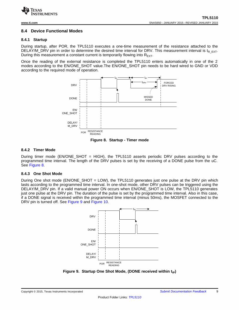
8.4 Device Functional Modes
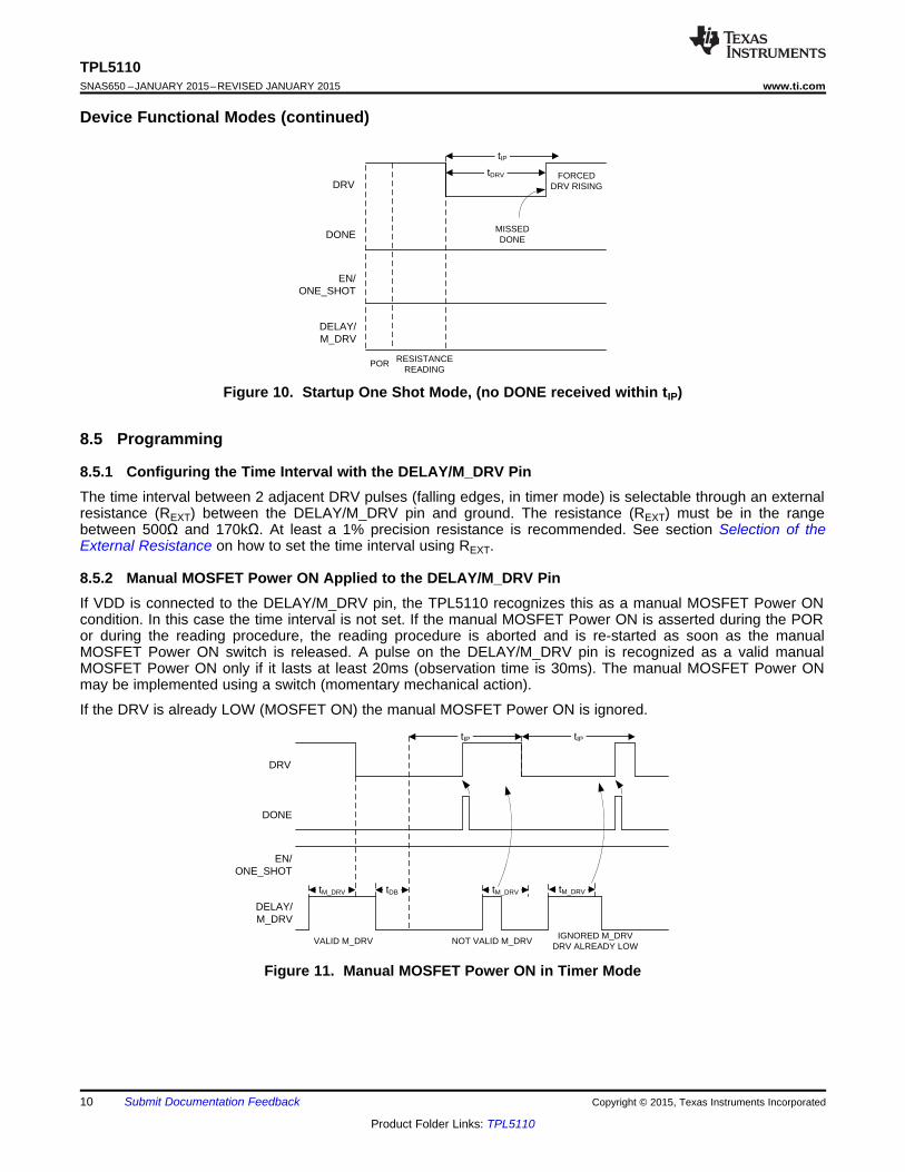
8.4.1 StartupDuring startup, after POR, the TPL5110 executes a one-time measurement of the resistance attached to theDELAY/M_DRV pin in order to determine the desired time interval for DRV. This measurement interval is tR_EXT.During this measurement a constant current is temporarily flowing into REXT.
Once the reading of the external resistance is completed the TPL5110 enters automatically in one of the 2modes according to the EN/ONE_SHOT value.The EN/ONE_SHOT pin needs to be hard wired to GND or VDDaccording to the required mode of operation.
Figure 8. Startup - Timer mode
8.4.2 Timer ModeDuring timer mode (EN/ONE_SHOT = HIGH), the TPL5110 asserts periodic DRV pulses according to theprogrammed time interval. The length of the DRV pulses is set by the receiving of a DONE pulse from the uC.See Figure 8.
8.4.3 One Shot ModeDuring One shot mode (EN/ONE_SHOT = LOW), the TPL5110 generates just one pulse at the DRV pin whichlasts according to the programmed time interval. In one-shot mode, other DRV pulses can be triggered using theDELAY/M_DRV pin. If a valid manual power ON occurs when EN/ONE_SHOT is LOW, the TPL5110 generatesjust one pulse at the DRV pin. The duration of the pulse is set by the programmed time interval. Also in this case,if a DONE signal is received within the programmed time interval (minus 50ms), the MOSFET connected to theDRV pin is turned off. See Figure 9 and Figure 10.
Figure 9. Startup One Shot Mode, (DONE received within tIP)
DRV
DONE
EN/ONE_SHOT
DELAY/M_DRV
ttM_DRVt ttDBt ttM_DRVt
NOT VALID M_DRV VALID M_DRV
ttIPt
ttM_DRVt
IGNORED M_DRVDRV ALREADY LOW
ttIPt
DRV
DONE
EN/ONE_SHOT
DELAY/M_DRV
POR RESISTANCEREADING
ttIPt
ttDRVt
MISSEDDONE
FORCEDDRV RISING
10
TPL5110SNAS650 –JANUARY 2015–REVISED JANUARY 2015 www.ti.com
Product Folder Links: TPL5110
Submit Documentation Feedback Copyright © 2015, Texas Instruments Incorporated
Device Functional Modes (continued)
Figure 10. Startup One Shot Mode, (no DONE received within tIP)
8.5 Programming
8.5.1 Configuring the Time Interval with the DELAY/M_DRV PinThe time interval between 2 adjacent DRV pulses (falling edges, in timer mode) is selectable through an externalresistance (REXT) between the DELAY/M_DRV pin and ground. The resistance (REXT) must be in the rangebetween 500Ω and 170kΩ. At least a 1% precision resistance is recommended. See section Selection of theExternal Resistance on how to set the time interval using REXT.
8.5.2 Manual MOSFET Power ON Applied to the DELAY/M_DRV PinIf VDD is connected to the DELAY/M_DRV pin, the TPL5110 recognizes this as a manual MOSFET Power ONcondition. In this case the time interval is not set. If the manual MOSFET Power ON is asserted during the PORor during the reading procedure, the reading procedure is aborted and is re-started as soon as the manualMOSFET Power ON switch is released. A pulse on the DELAY/M_DRV pin is recognized as a valid manualMOSFET Power ON only if it lasts at least 20ms (observation time is 30ms). The manual MOSFET Power ONmay be implemented using a switch (momentary mechanical action).
If the DRV is already LOW (MOSFET ON) the manual MOSFET Power ON is ignored.
Figure 11. Manual MOSFET Power ON in Timer Mode
DRV
DONE
EN/ONE_SHOT
DELAY/M_DRV
ttM_DRVt ttDBt ttM_DRVt
NOT VALID M_DRV VALID M_DRV
ttIPt
11
TPL5110www.ti.com SNAS650 –JANUARY 2015–REVISED JANUARY 2015
Product Folder Links: TPL5110
Submit Documentation FeedbackCopyright © 2015, Texas Instruments Incorporated
Programming (continued)
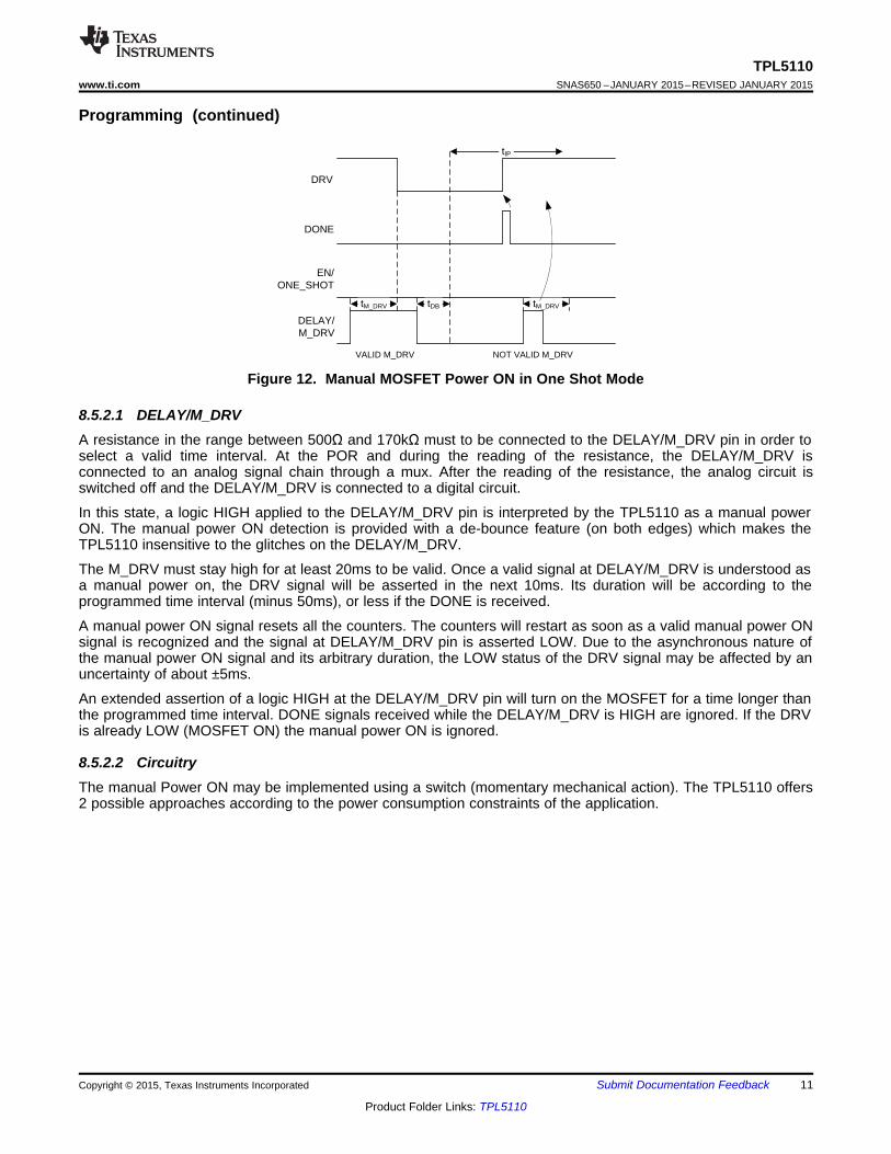
Figure 12. Manual MOSFET Power ON in One Shot Mode
8.5.2.1 DELAY/M_DRVA resistance in the range between 500Ω and 170kΩ must to be connected to the DELAY/M_DRV pin in order toselect a valid time interval. At the POR and during the reading of the resistance, the DELAY/M_DRV isconnected to an analog signal chain through a mux. After the reading of the resistance, the analog circuit isswitched off and the DELAY/M_DRV is connected to a digital circuit.
In this state, a logic HIGH applied to the DELAY/M_DRV pin is interpreted by the TPL5110 as a manual powerON. The manual power ON detection is provided with a de-bounce feature (on both edges) which makes theTPL5110 insensitive to the glitches on the DELAY/M_DRV.
The M_DRV must stay high for at least 20ms to be valid. Once a valid signal at DELAY/M_DRV is understood asa manual power on, the DRV signal will be asserted in the next 10ms. Its duration will be according to theprogrammed time interval (minus 50ms), or less if the DONE is received.
A manual power ON signal resets all the counters. The counters will restart as soon as a valid manual power ONsignal is recognized and the signal at DELAY/M_DRV pin is asserted LOW. Due to the asynchronous nature ofthe manual power ON signal and its arbitrary duration, the LOW status of the DRV signal may be affected by anuncertainty of about ±5ms.
An extended assertion of a logic HIGH at the DELAY/M_DRV pin will turn on the MOSFET for a time longer thanthe programmed time interval. DONE signals received while the DELAY/M_DRV is HIGH are ignored. If the DRVis already LOW (MOSFET ON) the manual power ON is ignored.
8.5.2.2 CircuitryThe manual Power ON may be implemented using a switch (momentary mechanical action). The TPL5110 offers2 possible approaches according to the power consumption constraints of the application.
¸¸
¹
·
¨¨
©
§
a
TcabbR EXT 2
1004100
2
VIN
POWER MANAGEMENT
VOUT
GND
µC
GPIO
VDD
GND
TPL5110
VDD
GND
EN/ONE_SHOT
DRV
DELAY/M_DRV
DONE
REXT
Battery
-+
VIN
POWER MANAGEMENT
VOUT
GND
µC
GPIO
VDD
GND
TPL5110
VDD
GND
EN/ONE_SHOT
DRV
DELAY/M_DRV
DONE
REXT
Battery
-+
12
TPL5110SNAS650 –JANUARY 2015–REVISED JANUARY 2015 www.ti.com
Product Folder Links: TPL5110
Submit Documentation Feedback Copyright © 2015, Texas Instruments Incorporated
Programming (continued)
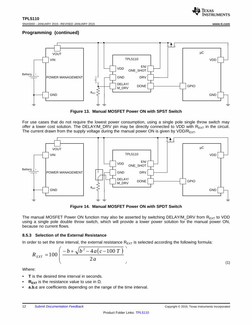
Figure 13. Manual MOSFET Power ON with SPST Switch
For use cases that do not require the lowest power consumption, using a single pole single throw switch mayoffer a lower cost solution. The DELAY/M_DRV pin may be directly connected to VDD with REXT in the circuit.The current drawn from the supply voltage during the manual power ON is given by VDD/REXT.
Figure 14. Manual MOSFET Power ON with SPDT Switch
The manual MOSFET Power ON function may also be asserted by switching DELAY/M_DRV from REXT to VDDusing a single pole double throw switch, which will provide a lower power solution for the manual power ON,because no current flows.
8.5.3 Selection of the External ResistanceIn order to set the time interval, the external resistance REXT is selected according the following formula:
(1)
Where:
• T is the desired time interval in seconds.• REXT is the resistance value to use in Ω.• a,b,c are coefficients depending on the range of the time interval.
¸¸
¹
·
¨¨
©
§
1284.0*2
8*1008889.25611284.0*49861.469861.46100
2
EXTR
13
TPL5110www.ti.com SNAS650 –JANUARY 2015–REVISED JANUARY 2015
Product Folder Links: TPL5110
Submit Documentation FeedbackCopyright © 2015, Texas Instruments Incorporated
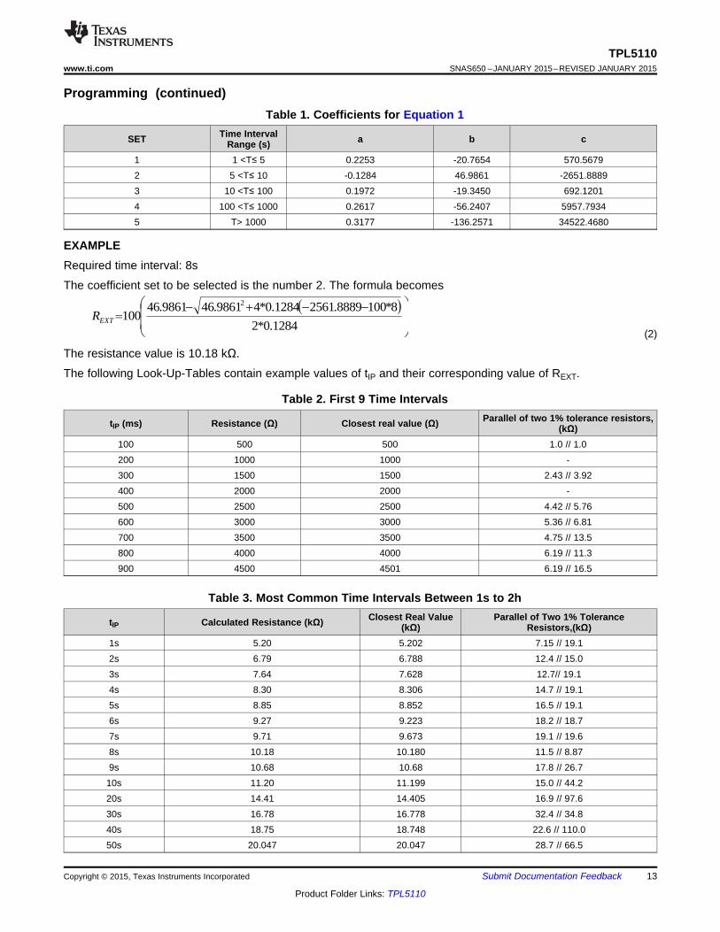
Programming (continued)Table 1. Coefficients for Equation 1
SET Time IntervalRange (s) a b c
1 1 <T≤ 5 0.2253 -20.7654 570.56792 5 <T≤ 10 -0.1284 46.9861 -2651.88893 10 <T≤ 100 0.1972 -19.3450 692.12014 100 <T≤ 1000 0.2617 -56.2407 5957.79345 T> 1000 0.3177 -136.2571 34522.4680
EXAMPLERequired time interval: 8s
The coefficient set to be selected is the number 2. The formula becomes
(2)
The resistance value is 10.18 kΩ.
The following Look-Up-Tables contain example values of tIP and their corresponding value of REXT.
Table 2. First 9 Time Intervals
tIP (ms) Resistance (Ω) Closest real value (Ω) Parallel of two 1% tolerance resistors,(kΩ)
100 500 500 1.0 // 1.0200 1000 1000 -300 1500 1500 2.43 // 3.92400 2000 2000 -500 2500 2500 4.42 // 5.76600 3000 3000 5.36 // 6.81700 3500 3500 4.75 // 13.5800 4000 4000 6.19 // 11.3900 4500 4501 6.19 // 16.5
Table 3. Most Common Time Intervals Between 1s to 2h
tIP Calculated Resistance (kΩ) Closest Real Value(kΩ)
Parallel of Two 1% ToleranceResistors,(kΩ)
1s 5.20 5.202 7.15 // 19.12s 6.79 6.788 12.4 // 15.03s 7.64 7.628 12.7// 19.14s 8.30 8.306 14.7 // 19.15s 8.85 8.852 16.5 // 19.16s 9.27 9.223 18.2 // 18.77s 9.71 9.673 19.1 // 19.68s 10.18 10.180 11.5 // 8.879s 10.68 10.68 17.8 // 26.7
10s 11.20 11.199 15.0 // 44.220s 14.41 14.405 16.9 // 97.630s 16.78 16.778 32.4 // 34.840s 18.75 18.748 22.6 // 110.050s 20.047 20.047 28.7 // 66.5
»¼
º«¬
ª
100EXT
D
RINTR
»¼
º«¬
ª¸¹
ᬩ
§ c
Rb
RaINTT DD
ADC 100100100
12
2
DESIRED
ADCDESIRED
T
TTErr
100
14
TPL5110SNAS650 –JANUARY 2015–REVISED JANUARY 2015 www.ti.com
Product Folder Links: TPL5110
Submit Documentation Feedback Copyright © 2015, Texas Instruments Incorporated
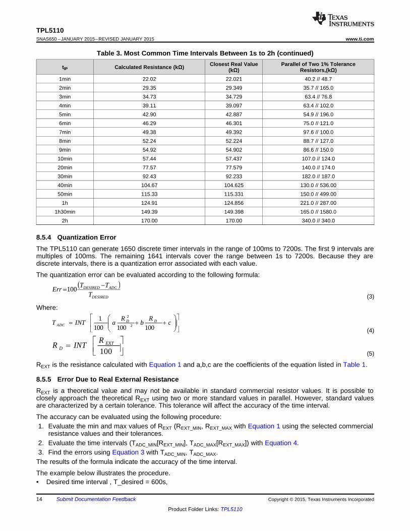
Table 3. Most Common Time Intervals Between 1s to 2h (continued)
tIP Calculated Resistance (kΩ) Closest Real Value(kΩ)
Parallel of Two 1% ToleranceResistors,(kΩ)
1min 22.02 22.021 40.2 // 48.72min 29.35 29.349 35.7 // 165.03min 34.73 34.729 63.4 // 76.84min 39.11 39.097 63.4 // 102.05min 42.90 42.887 54.9 // 196.06min 46.29 46.301 75.0 // 121.07min 49.38 49.392 97.6 // 100.08min 52.24 52.224 88.7 // 127.09min 54.92 54.902 86.6 // 150.010min 57.44 57.437 107.0 // 124.020min 77.57 77.579 140.0 // 174.030min 92.43 92.233 182.0 // 187.040min 104.67 104.625 130.0 // 536.0050min 115.33 115.331 150.0 // 499.00
1h 124.91 124.856 221.0 // 287.001h30min 149.39 149.398 165.0 // 1580.0
2h 170.00 170.00 340.0 // 340.0
8.5.4 Quantization ErrorThe TPL5110 can generate 1650 discrete timer intervals in the range of 100ms to 7200s. The first 9 intervals aremultiples of 100ms. The remaining 1641 intervals cover the range between 1s to 7200s. Because they arediscrete intervals, there is a quantization error associated with each value.
The quantization error can be evaluated according to the following formula:
(3)
Where:
(4)
(5)
REXT is the resistance calculated with Equation 1 and a,b,c are the coefficients of the equation listed in Table 1.
8.5.5 Error Due to Real External ResistanceREXT is a theoretical value and may not be available in standard commercial resistor values. It is possible toclosely approach the theoretical REXT using two or more standard values in parallel. However, standard valuesare characterized by a certain tolerance. This tolerance will affect the accuracy of the time interval.
The accuracy can be evaluated using the following procedure:1. Evaluate the min and max values of REXT (REXT_MIN, REXT_MAX with Equation 1 using the selected commercial
resistance values and their tolerances.2. Evaluate the time intervals (TADC_MIN[REXT_MIN], TADC_MAX[REXT_MAX]) with Equation 4.3. Find the errors using Equation 3 with TADC_MIN, TADC_MAX.
The results of the formula indicate the accuracy of the time interval.
The example below illustrates the procedure.• Desired time interval , T_desired = 600s,
3
ToleranceRnu nR
2
2
2
1//// 21
¸¹
ᬩ
§¸
¹
ᬩ
§
R
u
R
uRuR RR
15
TPL5110www.ti.com SNAS650 –JANUARY 2015–REVISED JANUARY 2015
Product Folder Links: TPL5110
Submit Documentation FeedbackCopyright © 2015, Texas Instruments Incorporated
• Required REXT, from Equation 1, REXT= 57.44kΩ.
From Table 3 REXT can be built with a parallel combination of two commercial values with 1% tolerance:R1=107kΩ, R2=124kΩ. The uncertainty of the equivalent parallel resistance can be found using:
(6)
Where uRn (n=1,2) represent the uncertainty of a resistance,
(7)
The uncertainty of the parallel resistance is 0.82%, meaning the value of REXT may range between REXT_MIN =56.96 kΩ and REXT_MAX = 57.90 kΩ.
Using these value of REXT, the digitized timer intervals calculated with Equation 4 are respectively TADC_MIN =586.85 s and TADC_MAX = 611.3 s, giving an error range of -1.88% / +2.19%. The asymmetry of the error range isdue to the quadratic transfer function of the resistance digitizer.
VDD
TPL5110
GND
DELAY/M_DRV
EN/ONE_SHOT
DRV
DONE
VDD
CC2531
GPIO
RF
GND
VDD
HDC1000
SCL
SDA
GND
SCL
SDA
DC-DCBOOST
ENB
VOUTVIN
Rp100k
Rp100k
Lithium ion battery
-
+
GND
16
TPL5110SNAS650 –JANUARY 2015–REVISED JANUARY 2015 www.ti.com
Product Folder Links: TPL5110
Submit Documentation Feedback Copyright © 2015, Texas Instruments Incorporated
9 Application and Implementation
NOTEInformation in the following applications sections is not part of the TI componentspecification, and TI does not warrant its accuracy or completeness. TI’s customers areresponsible for determining suitability of components for their purposes. Customers shouldvalidate and test their design implementation to confirm system functionality.
9.1 Application InformationIn battery powered applications one design constraint is the need for low current consumption. The TPL5110 issuitable in applications where there is a need to monitor environmental conditions at a fixed time interval. Oftenin these applications a watchdog or other internal timer in a µC is used to implement a wakeup function.Typically, the power consumption of these functions is not optimized. Using the TPL5110 to implement aperiodical power gating of the µC or of the entire system the current consumption will be only tens of nA.
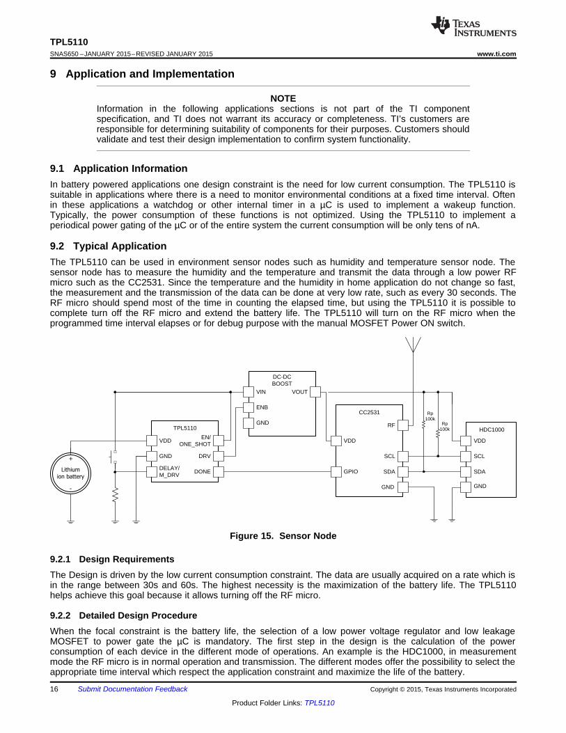
9.2 Typical ApplicationThe TPL5110 can be used in environment sensor nodes such as humidity and temperature sensor node. Thesensor node has to measure the humidity and the temperature and transmit the data through a low power RFmicro such as the CC2531. Since the temperature and the humidity in home application do not change so fast,the measurement and the transmission of the data can be done at very low rate, such as every 30 seconds. TheRF micro should spend most of the time in counting the elapsed time, but using the TPL5110 it is possible tocomplete turn off the RF micro and extend the battery life. The TPL5110 will turn on the RF micro when theprogrammed time interval elapses or for debug purpose with the manual MOSFET Power ON switch.
Figure 15. Sensor Node
9.2.1 Design RequirementsThe Design is driven by the low current consumption constraint. The data are usually acquired on a rate which isin the range between 30s and 60s. The highest necessity is the maximization of the battery life. The TPL5110helps achieve this goal because it allows turning off the RF micro.
9.2.2 Detailed Design ProcedureWhen the focal constraint is the battery life, the selection of a low power voltage regulator and low leakageMOSFET to power gate the µC is mandatory. The first step in the design is the calculation of the powerconsumption of each device in the different mode of operations. An example is the HDC1000, in measurementmode the RF micro is in normal operation and transmission. The different modes offer the possibility to select theappropriate time interval which respect the application constraint and maximize the life of the battery.
Time
Cu
rren
t co
nsu
mp
tio
n
Without TPL5110With TPL5110
17
TPL5110www.ti.com SNAS650 –JANUARY 2015–REVISED JANUARY 2015
Product Folder Links: TPL5110
Submit Documentation FeedbackCopyright © 2015, Texas Instruments Incorporated
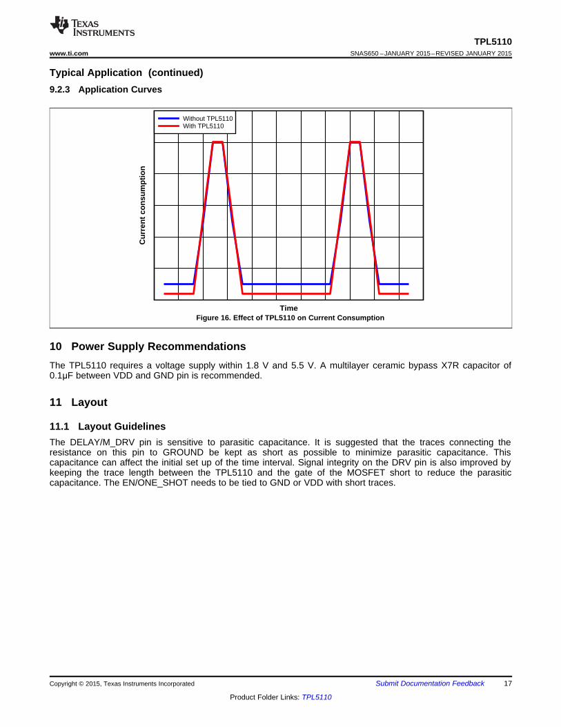
Typical Application (continued)9.2.3 Application Curves
Figure 16. Effect of TPL5110 on Current Consumption
10 Power Supply RecommendationsThe TPL5110 requires a voltage supply within 1.8 V and 5.5 V. A multilayer ceramic bypass X7R capacitor of0.1μF between VDD and GND pin is recommended.
11 Layout
11.1 Layout GuidelinesThe DELAY/M_DRV pin is sensitive to parasitic capacitance. It is suggested that the traces connecting theresistance on this pin to GROUND be kept as short as possible to minimize parasitic capacitance. Thiscapacitance can affect the initial set up of the time interval. Signal integrity on the DRV pin is also improved bykeeping the trace length between the TPL5110 and the gate of the MOSFET short to reduce the parasiticcapacitance. The EN/ONE_SHOT needs to be tied to GND or VDD with short traces.
18
TPL5110SNAS650 –JANUARY 2015–REVISED JANUARY 2015 www.ti.com
Product Folder Links: TPL5110
Submit Documentation Feedback Copyright © 2015, Texas Instruments Incorporated
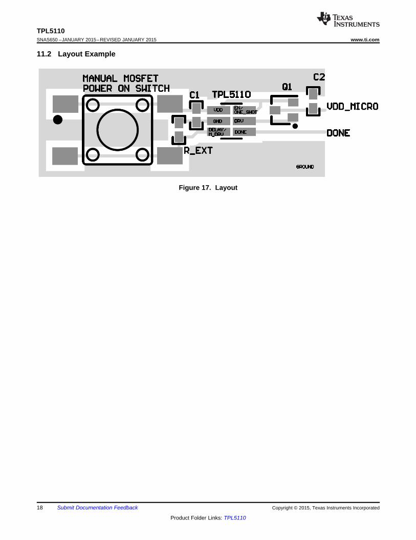
11.2 Layout Example
Figure 17. Layout
19
TPL5110www.ti.com SNAS650 –JANUARY 2015–REVISED JANUARY 2015
Product Folder Links: TPL5110
Submit Documentation FeedbackCopyright © 2015, Texas Instruments Incorporated
12 Device and Documentation Support
12.1 TrademarksAll trademarks are the property of their respective owners.
12.2 Electrostatic Discharge CautionThese devices have limited built-in ESD protection. The leads should be shorted together or the device placed in conductive foamduring storage or handling to prevent electrostatic damage to the MOS gates.
12.3 GlossarySLYZ022 — TI Glossary.
This glossary lists and explains terms, acronyms, and definitions.
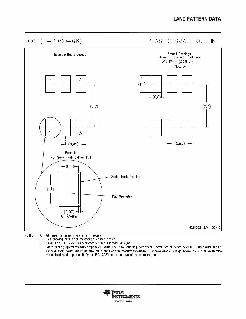
13 Mechanical, Packaging, and Orderable InformationThe following pages include mechanical, packaging, and orderable information. This information is the mostcurrent data available for the designated devices. This data is subject to change without notice and revision ofthis document. For browser-based versions of this data sheet, refer to the left-hand navigation.
PACKAGE OPTION ADDENDUM
www.ti.com 16-Jan-2015
Addendum-Page 1
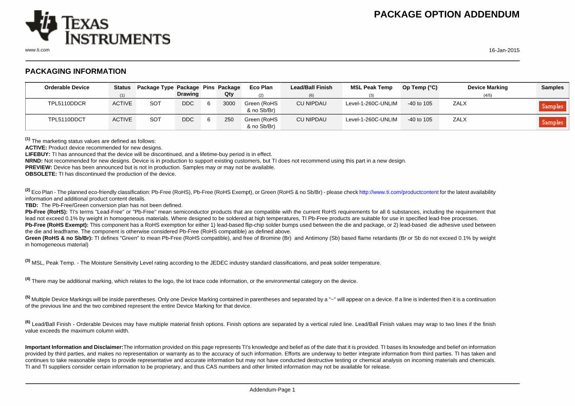
PACKAGING INFORMATION
Orderable Device Status(1)
Package Type PackageDrawing
Pins PackageQty
Eco Plan(2)
Lead/Ball Finish(6)
MSL Peak Temp(3)
Op Temp (°C) Device Marking(4/5)
Samples
TPL5110DDCR ACTIVE SOT DDC 6 3000 Green (RoHS& no Sb/Br)
CU NIPDAU Level-1-260C-UNLIM -40 to 105 ZALX
TPL5110DDCT ACTIVE SOT DDC 6 250 Green (RoHS& no Sb/Br)
CU NIPDAU Level-1-260C-UNLIM -40 to 105 ZALX
(1) The marketing status values are defined as follows:ACTIVE: Product device recommended for new designs.LIFEBUY: TI has announced that the device will be discontinued, and a lifetime-buy period is in effect.NRND: Not recommended for new designs. Device is in production to support existing customers, but TI does not recommend using this part in a new design.PREVIEW: Device has been announced but is not in production. Samples may or may not be available.OBSOLETE: TI has discontinued the production of the device.
(2) Eco Plan - The planned eco-friendly classification: Pb-Free (RoHS), Pb-Free (RoHS Exempt), or Green (RoHS & no Sb/Br) - please check http://www.ti.com/productcontent for the latest availabilityinformation and additional product content details.TBD: The Pb-Free/Green conversion plan has not been defined.Pb-Free (RoHS): TI's terms "Lead-Free" or "Pb-Free" mean semiconductor products that are compatible with the current RoHS requirements for all 6 substances, including the requirement thatlead not exceed 0.1% by weight in homogeneous materials. Where designed to be soldered at high temperatures, TI Pb-Free products are suitable for use in specified lead-free processes.Pb-Free (RoHS Exempt): This component has a RoHS exemption for either 1) lead-based flip-chip solder bumps used between the die and package, or 2) lead-based die adhesive used betweenthe die and leadframe. The component is otherwise considered Pb-Free (RoHS compatible) as defined above.Green (RoHS & no Sb/Br): TI defines "Green" to mean Pb-Free (RoHS compatible), and free of Bromine (Br) and Antimony (Sb) based flame retardants (Br or Sb do not exceed 0.1% by weightin homogeneous material)
(3) MSL, Peak Temp. - The Moisture Sensitivity Level rating according to the JEDEC industry standard classifications, and peak solder temperature.
(4) There may be additional marking, which relates to the logo, the lot trace code information, or the environmental category on the device.
(5) Multiple Device Markings will be inside parentheses. Only one Device Marking contained in parentheses and separated by a "~" will appear on a device. If a line is indented then it is a continuationof the previous line and the two combined represent the entire Device Marking for that device.
(6) Lead/Ball Finish - Orderable Devices may have multiple material finish options. Finish options are separated by a vertical ruled line. Lead/Ball Finish values may wrap to two lines if the finishvalue exceeds the maximum column width.
Important Information and Disclaimer:The information provided on this page represents TI's knowledge and belief as of the date that it is provided. TI bases its knowledge and belief on informationprovided by third parties, and makes no representation or warranty as to the accuracy of such information. Efforts are underway to better integrate information from third parties. TI has taken andcontinues to take reasonable steps to provide representative and accurate information but may not have conducted destructive testing or chemical analysis on incoming materials and chemicals.TI and TI suppliers consider certain information to be proprietary, and thus CAS numbers and other limited information may not be available for release.
PACKAGE OPTION ADDENDUM
www.ti.com 16-Jan-2015
Addendum-Page 2
In no event shall TI's liability arising out of such information exceed the total purchase price of the TI part(s) at issue in this document sold by TI to Customer on an annual basis.
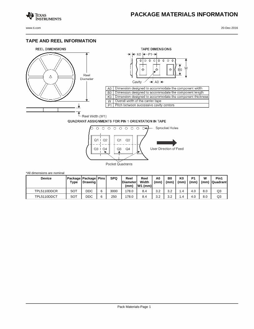
TAPE AND REEL INFORMATION
*All dimensions are nominal
Device PackageType
PackageDrawing
Pins SPQ ReelDiameter
(mm)
ReelWidth
W1 (mm)
A0(mm)
B0(mm)
K0(mm)
P1(mm)
W(mm)
Pin1Quadrant
TPL5110DDCR SOT DDC 6 3000 178.0 8.4 3.2 3.2 1.4 4.0 8.0 Q3
TPL5110DDCT SOT DDC 6 250 178.0 8.4 3.2 3.2 1.4 4.0 8.0 Q3
PACKAGE MATERIALS INFORMATION
www.ti.com 20-Dec-2016
Pack Materials-Page 1
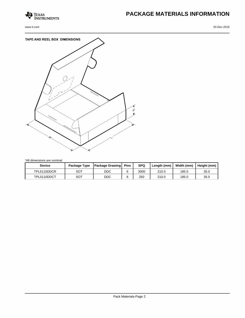
*All dimensions are nominal
Device Package Type Package Drawing Pins SPQ Length (mm) Width (mm) Height (mm)
TPL5110DDCR SOT DDC 6 3000 210.0 185.0 35.0
TPL5110DDCT SOT DDC 6 250 210.0 185.0 35.0
PACKAGE MATERIALS INFORMATION
www.ti.com 20-Dec-2016
Pack Materials-Page 2
IMPORTANT NOTICE
Texas Instruments Incorporated and its subsidiaries (TI) reserve the right to make corrections, enhancements, improvements and otherchanges to its semiconductor products and services per JESD46, latest issue, and to discontinue any product or service per JESD48, latestissue. Buyers should obtain the latest relevant information before placing orders and should verify that such information is current andcomplete. All semiconductor products (also referred to herein as “components”) are sold subject to TI’s terms and conditions of salesupplied at the time of order acknowledgment.TI warrants performance of its components to the specifications applicable at the time of sale, in accordance with the warranty in TI’s termsand conditions of sale of semiconductor products. Testing and other quality control techniques are used to the extent TI deems necessaryto support this warranty. Except where mandated by applicable law, testing of all parameters of each component is not necessarilyperformed.TI assumes no liability for applications assistance or the design of Buyers’ products. Buyers are responsible for their products andapplications using TI components. To minimize the risks associated with Buyers’ products and applications, Buyers should provideadequate design and operating safeguards.TI does not warrant or represent that any license, either express or implied, is granted under any patent right, copyright, mask work right, orother intellectual property right relating to any combination, machine, or process in which TI components or services are used. Informationpublished by TI regarding third-party products or services does not constitute a license to use such products or services or a warranty orendorsement thereof. Use of such information may require a license from a third party under the patents or other intellectual property of thethird party, or a license from TI under the patents or other intellectual property of TI.Reproduction of significant portions of TI information in TI data books or data sheets is permissible only if reproduction is without alterationand is accompanied by all associated warranties, conditions, limitations, and notices. TI is not responsible or liable for such altereddocumentation. Information of third parties may be subject to additional restrictions.Resale of TI components or services with statements different from or beyond the parameters stated by TI for that component or servicevoids all express and any implied warranties for the associated TI component or service and is an unfair and deceptive business practice.TI is not responsible or liable for any such statements.Buyer acknowledges and agrees that it is solely responsible for compliance with all legal, regulatory and safety-related requirementsconcerning its products, and any use of TI components in its applications, notwithstanding any applications-related information or supportthat may be provided by TI. Buyer represents and agrees that it has all the necessary expertise to create and implement safeguards whichanticipate dangerous consequences of failures, monitor failures and their consequences, lessen the likelihood of failures that might causeharm and take appropriate remedial actions. Buyer will fully indemnify TI and its representatives against any damages arising out of the useof any TI components in safety-critical applications.In some cases, TI components may be promoted specifically to facilitate safety-related applications. With such components, TI’s goal is tohelp enable customers to design and create their own end-product solutions that meet applicable functional safety standards andrequirements. Nonetheless, such components are subject to these terms.No TI components are authorized for use in FDA Class III (or similar life-critical medical equipment) unless authorized officers of the partieshave executed a special agreement specifically governing such use.Only those TI components which TI has specifically designated as military grade or “enhanced plastic” are designed and intended for use inmilitary/aerospace applications or environments. Buyer acknowledges and agrees that any military or aerospace use of TI componentswhich have not been so designated is solely at the Buyer's risk, and that Buyer is solely responsible for compliance with all legal andregulatory requirements in connection with such use.TI has specifically designated certain components as meeting ISO/TS16949 requirements, mainly for automotive use. In any case of use ofnon-designated products, TI will not be responsible for any failure to meet ISO/TS16949.
Products ApplicationsAudio www.ti.com/audio Automotive and Transportation www.ti.com/automotiveAmplifiers amplifier.ti.com Communications and Telecom www.ti.com/communicationsData Converters dataconverter.ti.com Computers and Peripherals www.ti.com/computersDLP® Products www.dlp.com Consumer Electronics www.ti.com/consumer-appsDSP dsp.ti.com Energy and Lighting www.ti.com/energyClocks and Timers www.ti.com/clocks Industrial www.ti.com/industrialInterface interface.ti.com Medical www.ti.com/medicalLogic logic.ti.com Security www.ti.com/securityPower Mgmt power.ti.com Space, Avionics and Defense www.ti.com/space-avionics-defenseMicrocontrollers microcontroller.ti.com Video and Imaging www.ti.com/videoRFID www.ti-rfid.comOMAP Applications Processors www.ti.com/omap TI E2E Community e2e.ti.comWireless Connectivity www.ti.com/wirelessconnectivity
Mailing Address: Texas Instruments, Post Office Box 655303, Dallas, Texas 75265Copyright © 2016, Texas Instruments Incorporated